AC Modeling of Power Stage in Flyback Converter - TI.com · SLVA589 2 AC Modeling of Power Stage in...
12
Application Report SLVA589 – July 2013 1 AC Modeling of Power Stage in Flyback Converter Rushil K K PWR-DCDC Controllers ABSTRACT This application report provides a step-by-step procedure for constructing the AC model for the power stage of a Flyback DC/DC Converter in Continuous Conduction Mode. The model is used in the TIna simulator to plot and verify the control-to-output transfer function. Contents 1 Introduction .................................................................................................................................. 1 1.1 How it Works .......................................................................................................................... 2 2 Circuit Manipulations ................................................................................................................... 3 3 Construction of the Mathematical Model .................................................................................... 5 4 Simulation and Results ................................................................................................................ 8 5 Conclusion: ................................................................................................................................ 11 Figures Figure 1. Basic Topology of Flyback Converter ............................................................................ 2 Figure 2. Separating Out the Non-Linear Switch Elements .......................................................... 3 Figure 3. Voltage Waveforms for the 2-Port Network.................................................................... 4 Figure 4. Current Waveforms for the 2-Port Network.................................................................... 4 Figure 5. Replacing the Non-Linear Switch Network with Equivalent Linear Network ............... 7 Figure 6. Complete Linear Circuit for Flyback Converter ............................................................. 8 Figure 7. Implementation of Example Case in Tina Simulator ................................................... 10 Figure 8. Control-to-Output Transfer Function Plotted using TIna ............................................ 11 1 Introduction The flyback DC-DC converter is derived from the basic buck-boost converter. The conversion ratio for this converter is given by, = . 1 − As seen from this equation, the conversion ratio is similar to that of the buck-boost converter with an included factor of n, which is the turns ratio of the flyback transformer.
Transcript of AC Modeling of Power Stage in Flyback Converter - TI.com · SLVA589 2 AC Modeling of Power Stage in...

Application Report SLVA589 – July 2013
1
AC Modeling of Power Stage in Flyback Converter Rushil K K PWR-DCDC Controllers
ABSTRACT
This application report provides a step-by-step procedure for constructing the AC model for the power stage of a Flyback DC/DC Converter in Continuous Conduction Mode. The model is used in the TIna simulator to plot and verify the control-to-output transfer function.
Contents 1 Introduction .................................................................................................................................. 1
1.1 How it Works .......................................................................................................................... 2 2 Circuit Manipulations ................................................................................................................... 3 3 Construction of the Mathematical Model .................................................................................... 5 4 Simulation and Results ................................................................................................................ 8 5 Conclusion: ................................................................................................................................ 11
Figures Figure 1. Basic Topology of Flyback Converter ............................................................................ 2 Figure 2. Separating Out the Non-Linear Switch Elements .......................................................... 3 Figure 3. Voltage Waveforms for the 2-Port Network.................................................................... 4 Figure 4. Current Waveforms for the 2-Port Network.................................................................... 4 Figure 5. Replacing the Non-Linear Switch Network with Equivalent Linear Network ............... 7 Figure 6. Complete Linear Circuit for Flyback Converter ............................................................. 8 Figure 7. Implementation of Example Case in Tina Simulator ................................................... 10 Figure 8. Control-to-Output Transfer Function Plotted using TIna ............................................ 11
1 Introduction The flyback DC-DC converter is derived from the basic buck-boost converter. The conversion ratio for this converter is given by,
𝑉𝑜𝑢𝑡𝑉𝑖𝑛 = 𝑛.
𝐷1 − 𝐷
As seen from this equation, the conversion ratio is similar to that of the buck-boost converter with an included factor of n, which is the turns ratio of the flyback transformer.
a0193208
Stamp

SLVA589
2 AC Modeling of Power Stage in Flyback Converter
1.1 How it Works
In a flyback converter, when the current ramps up in the primary, energy is built up in the transformer core. When the FET switches off, this energy is dumped into the secondary, allowing current to flow in the secondary, so the primary current collapses immediately to zero. This causes an immediate rise in current in the secondary, after which, the current in the secondary ramps down linearly as it discharges, supplying energy to the load. The current in the secondary when the FET switches off, is proportional to the peak in the primary, and is determined by the turns ratio.
The circuit topology of the flyback converter is as shown in Figure 1.
Figure 1. Basic Topology of a Flyback Converter
SLVA589
AC Modeling of Power Stage in Flyback Converter 3
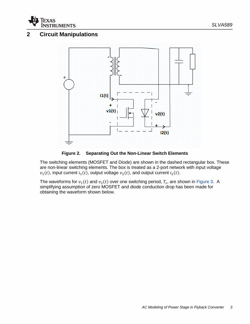
2 Circuit Manipulations The circuit can be re-drawn, to separate out the reactive components and the switching components, as shown in Figure 2.
Figure 2. Separating Out the Non-Linear Switch Elements
The switching elements (MOSFET and Diode) are shown in the dashed rectangular box. These are non-linear switching elements. The box is treated as a 2-port network with input voltage 𝑣1(𝑡), input current 𝑖1(𝑡), output voltage 𝑣2(𝑡), and output current 𝑖2(𝑡).
The waveforms for 𝑣1(𝑡) and 𝑣2(𝑡) over one switching period, 𝑇𝑠, are shown in Figure 3. A simplifying assumption of zero MOSFET and diode conduction drop has been made for obtaining the waveform shown below.

SLVA589
4 AC Modeling of Power Stage in Flyback Converter
Note: The slope of the voltage waveform in the figure is exaggerated for the sake of clarity.
Figure 3. Voltage Waveforms for the 2-Port Network
Similarly, the waveforms for 𝑖1(𝑡) and 𝑖2(𝑡) are shown in Figure 4.
Figure 4. Current Waveforms for the 2-Port Network

SLVA589
AC Modeling of Power Stage in Flyback Converter 5
3 Construction of the Mathematical Model The waveforms in Figure 3 and Figure 4 are averaged over one switching period, which effectively removes the switching harmonics. The switching harmonics have no role of consequence in the development of the AC model. Observing the waveform, it can be seen that:
< 𝑽𝟏(𝒕) >𝑻𝒔= 𝒅′(𝒕) ∗ {𝑽𝒊𝒏 + 𝑽𝒐 𝒏� } < 𝑽𝟐(𝒕) >𝑻𝒔= 𝒅(𝒕) ∗ {𝒏𝑽𝒊𝒏 + 𝑽𝒐 }
Dividing the above equations, we get the following relation:
< 𝑽𝟏(𝒕) >𝑻𝒔< 𝑽𝟐(𝒕) >𝑻𝒔� =
𝟏𝒏∗𝒅′(𝒕)𝒅(𝒕)
Hence, we have:
< 𝑽𝟏(𝒕) >𝑻𝒔 = 𝟏𝒏∗ 𝒅′(𝒕)𝒅(𝒕)
∗< 𝑽𝟐(𝒕) >𝑻𝒔 (1)
Equation 1 is a non-linear one, since it contains products of time-dependent variables. To obtain a linear relation, the variables are perturbed about the quiescent operating point.
𝒅(𝒕) = 𝐷 + �̂� < 𝑽𝟏(𝒕) >𝑻𝒔 = 𝑉1 + 𝑣1� < 𝑽𝟐(𝒕) >𝑻𝒔 = 𝑉2 + 𝑣2�
Using the preceding equations in (1):
𝑽𝟏 + 𝒗𝟏� = 𝟏𝒏∗𝐷′ − �̂�𝐷 + �̂�
∗ (𝑽𝟐 + 𝒗𝟐� )
𝑽𝟏 ∗ 𝑫 + 𝑽𝟏 ∗ 𝒅� + 𝒗𝟏� ∗𝑫+ 𝒗𝟏� ∗ 𝒅� = 𝟏𝒏 ∗ {𝑽𝟐 ∗ 𝑫′ − 𝑽𝟐 ∗ 𝒅� + 𝒗𝟐� ∗𝑫′ − 𝒗𝟐� ∗ 𝒅�}
Since the perturbations are small, the non-linear terms 𝒗𝟏� ∗ 𝒅� and 𝒗𝟐� ∗ 𝒅� are small enough to be ignored. Upon rearranging and grouping terms appropriately:
(2)
The equation is re-arranged into the below form,
(3)
Note: Equating the quiescent terms in Equation 2, we have 𝑽𝟏 ∗ 𝐷 = 𝟏𝒏𝑽𝟐 ∗ 𝑫′.
Substituting this relation for 𝑽𝟐 in Equation 3,
SLVA589
6 AC Modeling of Power Stage in Flyback Converter
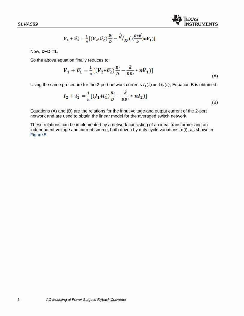
Now, D+D’=1.
So the above equation finally reduces to:
(A)
Using the same procedure for the 2-port network currents 𝑖1(𝑡) and 𝑖2(𝑡), Equation B is obtained:
(B)
Equations (A) and (B) are the relations for the input voltage and output current of the 2-port network and are used to obtain the linear model for the averaged switch network.
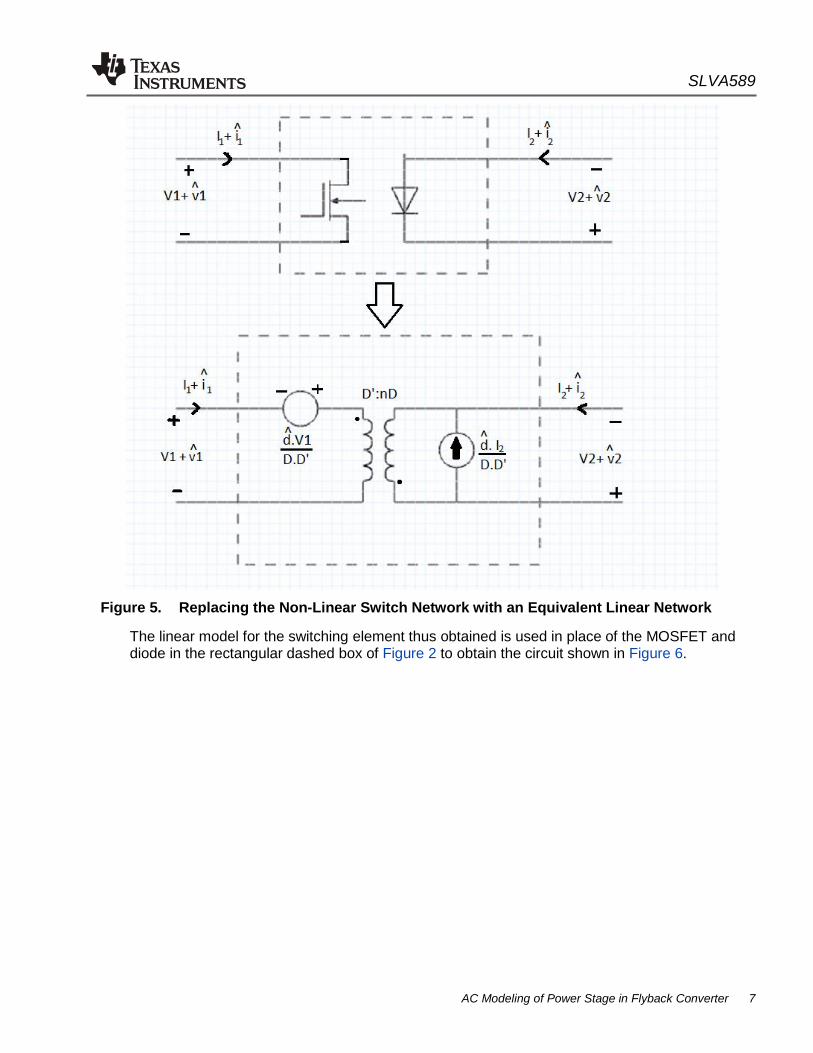
These relations can be implemented by a network consisting of an ideal transformer and an independent voltage and current source, both driven by duty cycle variations, d(t), as shown in Figure 5.
SLVA589
AC Modeling of Power Stage in Flyback Converter 7
Figure 5. Replacing the Non-Linear Switch Network with an Equivalent Linear Network
The linear model for the switching element thus obtained is used in place of the MOSFET and diode in the rectangular dashed box of Figure 2 to obtain the circuit shown in Figure 6.

SLVA589
8 AC Modeling of Power Stage in Flyback Converter
Figure 6. Complete Linear Circuit for Flyback Converter
The inductance 𝐿𝑀 indicates the magnetizing inductance, and is used with an ideal transformer of turns ratio 1:n.
4 Simulation and Results Example: Consider a flyback converter designed for the following specifications: 𝑉𝑖𝑛 = 5𝑉, 𝑉𝑜𝑢𝑡 = 10𝑉. A load resistance of 10 Ω is connected at the output, so the load current drawn is 1 A. The magnetizing inductance of the flyback transformer is 6 µH, and load capacitance used is 500 µF.
The turns ratio n=4, hence, the duty cycle, D, required to produce a 10-V output is D = 0.33.
The quiescent value for 𝑣1 (t), is 𝑉1 = 𝐷′. (𝑉𝑖𝑛 + 𝑉𝑜/𝑛), as seen from waveform.
Similarly, 𝐼2 = 𝐼𝑙𝑜𝑎𝑑
Hence, 𝑉1= 4.95 V.
Also, 𝐼2= 1 A.
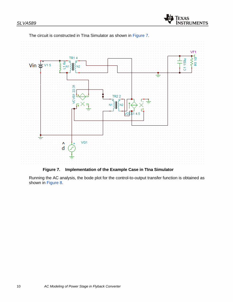
Now, for modeling in TIna, the voltage and current sources controlled by d(t) are implemented using the VCVS and VCCS sources respectively, as shown in Figure 7.
The gain of the VCVS source is set to be 𝑉1𝐷.𝐷′
(since the voltage source obtained in the derived
ac model is 𝑉1𝐷.𝐷′
∗ �̂�)
so, the gain of VCVS source is 22.31.

SLVA589
AC Modeling of Power Stage in Flyback Converter 9
The gain of VCCS source must be 𝐼2𝐷.𝐷′
(again, according to derived model).
The gain of VCCS source is calculated to be 4.5.
The turns ratio of the transformer (of the switch model) is nD/D’ = 2.
Verification:
For a flyback converter, the location of RHPZ and LC resonant pole, is at(1):
𝑓𝑅𝐻𝑃𝑍 = (𝑅𝑜 ∗ 𝐷′2)(𝑛2 ∗ 2𝜋 ∗ 𝐿𝑀 ∗ 𝐷)�
𝑓𝐿𝐶 = 𝐷′(𝑛 ∗ 2𝜋 ∗ �𝐿𝑀𝐶)�
Also, the gain at DC is, 𝐺𝑑0 = 𝑉0/𝐷𝐷′
Using the example values in the above equations, we should have the following:
𝑓𝑅𝐻𝑃𝑍 = 21.88 kHz
𝑓𝐿𝐶 = 883.3𝐻𝑧
𝐺𝑑0 = 45.09
𝐺𝑑0|𝑑𝐵 = 33.2𝑑𝐵
SLVA589
10 AC Modeling of Power Stage in Flyback Converter
The circuit is constructed in TIna Simulator as shown in Figure 7.
Figure 7. Implementation of the Example Case in TIna Simulator
Running the AC analysis, the bode plot for the control-to-output transfer function is obtained as shown in Figure 8.

SLVA589
AC Modeling of Power Stage in Flyback Converter 11
Figure 8. Control-to-Output Transfer Function Plotted using TIna
As seen from Figure 8, the LC resonant pole appears at around 862 Hz.
The RHPZ is located at around 22.13 kHz.
Gain at DC is 33 dB. Hence, it is seen that the response obtained from the model matches closely with the theoretical calculations.
5 Conclusion The AC model of the power stage for a flyback converter can be constructed following the steps shown in this application report. The response of the model, implemented in a TIna Simulator, is found to be in alignment with what is theoretically expected.
6 References 1. Basso, C., “How to Keep a FLYBACK Switch Mode Supply Stable with a Critical-Mode
Controller,” ON Semiconductor™, AN1681/D Application Note, September 2000 – Rev. 0

IMPORTANT NOTICE
Texas Instruments Incorporated and its subsidiaries (TI) reserve the right to make corrections, enhancements, improvements and otherchanges to its semiconductor products and services per JESD46, latest issue, and to discontinue any product or service per JESD48, latestissue. Buyers should obtain the latest relevant information before placing orders and should verify that such information is current andcomplete. All semiconductor products (also referred to herein as “components”) are sold subject to TI’s terms and conditions of salesupplied at the time of order acknowledgment.
TI warrants performance of its components to the specifications applicable at the time of sale, in accordance with the warranty in TI’s termsand conditions of sale of semiconductor products. Testing and other quality control techniques are used to the extent TI deems necessaryto support this warranty. Except where mandated by applicable law, testing of all parameters of each component is not necessarilyperformed.
TI assumes no liability for applications assistance or the design of Buyers’ products. Buyers are responsible for their products andapplications using TI components. To minimize the risks associated with Buyers’ products and applications, Buyers should provideadequate design and operating safeguards.
TI does not warrant or represent that any license, either express or implied, is granted under any patent right, copyright, mask work right, orother intellectual property right relating to any combination, machine, or process in which TI components or services are used. Informationpublished by TI regarding third-party products or services does not constitute a license to use such products or services or a warranty orendorsement thereof. Use of such information may require a license from a third party under the patents or other intellectual property of thethird party, or a license from TI under the patents or other intellectual property of TI.
Reproduction of significant portions of TI information in TI data books or data sheets is permissible only if reproduction is without alterationand is accompanied by all associated warranties, conditions, limitations, and notices. TI is not responsible or liable for such altereddocumentation. Information of third parties may be subject to additional restrictions.
Resale of TI components or services with statements different from or beyond the parameters stated by TI for that component or servicevoids all express and any implied warranties for the associated TI component or service and is an unfair and deceptive business practice.TI is not responsible or liable for any such statements.
Buyer acknowledges and agrees that it is solely responsible for compliance with all legal, regulatory and safety-related requirementsconcerning its products, and any use of TI components in its applications, notwithstanding any applications-related information or supportthat may be provided by TI. Buyer represents and agrees that it has all the necessary expertise to create and implement safeguards whichanticipate dangerous consequences of failures, monitor failures and their consequences, lessen the likelihood of failures that might causeharm and take appropriate remedial actions. Buyer will fully indemnify TI and its representatives against any damages arising out of the useof any TI components in safety-critical applications.
In some cases, TI components may be promoted specifically to facilitate safety-related applications. With such components, TI’s goal is tohelp enable customers to design and create their own end-product solutions that meet applicable functional safety standards andrequirements. Nonetheless, such components are subject to these terms.
No TI components are authorized for use in FDA Class III (or similar life-critical medical equipment) unless authorized officers of the partieshave executed a special agreement specifically governing such use.
Only those TI components which TI has specifically designated as military grade or “enhanced plastic” are designed and intended for use inmilitary/aerospace applications or environments. Buyer acknowledges and agrees that any military or aerospace use of TI componentswhich have not been so designated is solely at the Buyer's risk, and that Buyer is solely responsible for compliance with all legal andregulatory requirements in connection with such use.
TI has specifically designated certain components as meeting ISO/TS16949 requirements, mainly for automotive use. In any case of use ofnon-designated products, TI will not be responsible for any failure to meet ISO/TS16949.
Products Applications
Audio www.ti.com/audio Automotive and Transportation www.ti.com/automotive
Amplifiers amplifier.ti.com Communications and Telecom www.ti.com/communications
Data Converters dataconverter.ti.com Computers and Peripherals www.ti.com/computers
DLP® Products www.dlp.com Consumer Electronics www.ti.com/consumer-apps
DSP dsp.ti.com Energy and Lighting www.ti.com/energy
Clocks and Timers www.ti.com/clocks Industrial www.ti.com/industrial
Interface interface.ti.com Medical www.ti.com/medical
Logic logic.ti.com Security www.ti.com/security
Power Mgmt power.ti.com Space, Avionics and Defense www.ti.com/space-avionics-defense
Microcontrollers microcontroller.ti.com Video and Imaging www.ti.com/video
RFID www.ti-rfid.com
OMAP Applications Processors www.ti.com/omap TI E2E Community e2e.ti.com
Wireless Connectivity www.ti.com/wirelessconnectivity
Mailing Address: Texas Instruments, Post Office Box 655303, Dallas, Texas 75265Copyright © 2013, Texas Instruments Incorporated