FLYING CAPACITOR MULTILEVEL FLYBACK...
61
FLYING CAPACITOR MULTILEVEL FLYBACK CONVERTER by Santino Fiorello Graziani B.S. Electrical Engineering, University of Pittsburgh, 2016 Submitted to the Graduate Faculty of Swanson School of Engineering in partial fulfillment of the requirements for the degree of Master of Science University of Pittsburgh 2018
Transcript of FLYING CAPACITOR MULTILEVEL FLYBACK...

FLYING CAPACITOR MULTILEVEL FLYBACK CONVERTER
by
Santino Fiorello Graziani
B.S. Electrical Engineering, University of Pittsburgh, 2016
Submitted to the Graduate Faculty of
Swanson School of Engineering in partial fulfillment
of the requirements for the degree of
Master of Science
University of Pittsburgh
2018
ii
UNIVERSITY OF PITTSBURGH
SWANSON SCHOOL OF ENGINEERING
This thesis was presented
by
Santino Fiorello Graziani
It was defended on
June 12th, 2018
and approved by
Dr. Brandon Grainger, PhD., Assistant Professor, Department of Electrical and Computer
Engineering
Dr. Zhi-Hong Mao, PhD, Associate Professor, Department of Electrical and Computer
Engineering
Dr. Gregory Reed, PhD., Professor, Department of Electrical and Computer Engineering
Thesis Advisor: Dr. Brandon Grainger, PhD., Assistant Professor, Department of Electrical
and Computer Engineering

iii
Copyright © by Santino Fiorello Graziani
2018

iv
FLYING CAPACITOR MULTILEVEL FLYBACK CONVERTER
Santino Fiorello Graziani, M.S.
University of Pittsburgh, 2018
This work presents the development of a Flying Capacitor Multilevel Flyback Converter
(FCMFC) that provides easily scalable peak output voltage for pulsed power. Based on a
combination of the flyback and flying capacitor multilevel (FCML) boost converter topologies,
the FCMFC achieves faster slew rates and peak power than previous pulsed power converters.
The new converter improves on the conversion ratio of the flyback converter by a multiple of the
number of switched-diode-capacitor (SDC) cells. It distributes the high voltage gain across the
SDCs, lowering device stresses and reducing the required magnetic component size compared to
existing architectures. This makes FCMFC very attractive for DC-DC steady-state boosting
applications. To further this point the converter is analyzed in steady-state continuous conduction
mode (CCM) for component sizes and stresses. An FCMFC was developed to boost a 10V input
into 1000V output with half of the devices needed as compared to an existing FCML topology in
the literature. Another was developed for pulsed power to produce 36kV pulses at 8kV/µs, with a

v
50% decrease in the magnetic component size compared to an existing architecture from the
literature.

vi
TABLE OF CONTENTS PREFACE .................................................................................................................................... XI
1.0 INTRODUCTION ........................................................................................................ 1
2.0 DEVICE DESIGN REALIZATION .......................................................................... 4
2.1 FLYING CAPACITOR MODIFICATIONS .................................................... 5
2.2 SERIES FLYBACK CONFIGURATION ......................................................... 8
3.0 FLYING CAPACITOR MULTILEVEL FLYBACK CONVERTER .................. 11
3.1 TOPOLOGY DESIGN AND LAYOUT .......................................................... 12
3.2 STEADY-STATE ANALYSIS AND OPERATION IN CONTINUOUS
CONDUCTION MODE ............................................................................ 14
3.3 SWITCHING STRESS IN CCM...................................................................... 20
3.4 INDUCTOR SIZE ............................................................................................. 26
3.5 PULSED POWER OPERATION AND ANALYSIS IN DISCONTINUOUS
CONDUCTION MODE ............................................................................ 28
4.0 RESULTS AND DISCUSSION ................................................................................ 31
4.1 DC-DC STEADY-STATE RESULTS .............................................................. 32
4.1.1 Proving the Newly Found Conversion Ratio ............................................... 32
4.1.2 Optimizing to 7-Level FCML ....................................................................... 34
4.2 PULSED POWER RESULTS .......................................................................... 36

vii
4.2.1 Preliminary Pulsed Power Results ............................................................... 36
4.2.2 Optimizing to 10-level Series Flyback Converter ....................................... 38
5.0 CONCLUSIONS AND FUTURE WORK ............................................................... 41
APPENDIX A .............................................................................................................................. 43
APPENDIX B .............................................................................................................................. 44
APPENDIX C .............................................................................................................................. 47
BIBLIOGRAPHY ....................................................................................................................... 49

viii
LIST OF TABLES Table 1: Operating Modes of FCMFC (N = 3) ............................................................................. 15
Table 2: Steady-State DC-DC Step-Up FCMFC Converter Parameters ...................................... 32
Table 3: Output Voltage Average and Ripple Values for Various FCMFC Converter
Architectures ......................................................................................................... 33
Table 4: DC-DC Boosting Simulation Results ............................................................................. 34 Table 5: DC-DC Boosting Required Components ........................................................................ 35
Table 6: Component Values for FCMFC (3x2) ............................................................................ 36
Table 7: Simulation Results for Variations of Pulsed Power Topologies ..................................... 37
Table 8: Pulsed Power Simulation Results ................................................................................... 39
ix
LIST OF FIGURES Figure 2.1: 7-Level FCML Boost Topology ................................................................................... 5
Figure 2.2: Series Connected Flyback Converters .......................................................................... 9
Figure 2.3: Parallel Connected Flyback Converters ..................................................................... 10
Figure 3.1: Lowest Order FCMFC with a single SDC stage outlined in red ................................ 13
Figure 3.2: States 1 and 3 of FCMFC Operation: Charging Lm .................................................... 15
Figure 3.3: State 2 of FCMFC Operation: Charging C1 ............................................................... 15
Figure 3.4: State 4 of FCMFC Operation: Charging CO ............................................................... 15
Figure 3.5: Switching Diagram FCMFC (N = 3) .......................................................................... 16
Figure 3.6: Output Charging Circuit of FCMFC .......................................................................... 17
Figure 3.7: Available Gain for FCMFC ........................................................................................ 18
Figure 3.8: FCMFC Input Switch Stress Normalized to Flyback ................................................. 22
Figure 3.9: FCMFC Switch Utilization for FCMFC Converters .................................................. 23
Figure 3.10: FCMFC Secondary Side Individual Switch Stress (P = 1kW, n = 10)..................... 25
Figure 3.11: Required Magnetizing Inductance Normalized to Flyback Design ......................... 27
Figure 4.1: FCMFC Steady-State DC-DC Step-Up Results ......................................................... 33
Figure 4.2: DC-DC Boosting Simulation Results ......................................................................... 35
Figure 4.3: FCMFC (3x2) Pulsed Power Waveforms .................................................................. 37
Figure 4.4: 5x5 FCMFC for Pulsed Power ................................................................................... 39

x
Figure 5.1: Stage Voltages and Inductor Current; N = 5 Case...................................................... 45
Figure 5.2: FCMFC (5x1) Capacitor Charging States .................................................................. 45
Figure 5.3: Energy Available for Power Pulse of FCMFC ........................................................... 48

xi
PREFACE I would like to thank Dr. Brandon Grainger, my advisor, for all of the guidance over the past two
years. His dedication and thorough involvement was crucial in this research effort. I would also
like to thank Dr. Gregory Reed and Duquesne Light for my financial sponsorship. This allowed
me to dedicate my efforts towards research.
To my fellow graduate students in the Electric Power Systems Laboratory I would like to
give thanks. To Dr. Ansel Barchowsky, my PhD mentor, I would like to give special thanks.
Even with the stress of his new career (NASA Jet Propulsion Laboratory) he found the time to
have regular meetings and also review my conference papers before submission.
Thank you to my mother for all of the financial support over the years. Finally, I would
like to thank my fiancée Allison soon to be Graziani (Simons) for all of the emotional support
over the years. She has been with me throughout any and all struggles in, and out of, academia.

1
1.0 INTRODUCTION Demand has increased for small and robust power conversion electronics with the modernization
of the electric power grid. These devices are required to boost the low output voltage of
photovoltaic systems as well as wind energy harvesting systems [1]. This trend is not limited to
the energy sector. Countless systems rely on power electronic devices in industries including but
not limited to: medical, sanitation, auto, defense, and space exploration.
Power conversion electronics used in pulsed power applications require fast output rise
times to provide quick bursts of power to their loads. Pulsed power originated for military
weaponry, nuclear fusion, and x-ray technology, where medium voltage pulses, providing energy
in the mega-joule range, are required [2], [3]. Since then, pulsed power converters have been
adapted for various industrial applications including food processing, medical treatment, water
treatment, engine ignition, ion implantation, and more [4]. Designing from the experience with
high-voltage-pulsed-power applications, to these lower voltage industrial applications has led to
a shift from the utilization of gas and liquid spark gaps to semiconductors for handling the power
transfer [2], [5]. The load types mentioned are repetitive in nature and require an increase in the
repetition rate of the power pulse, which was not demanded by the early, “single shot”
applications. To meet these increasing demands, converters must be designed such that they
produce rapid power pulses, while minimizing component stress during operation. Many of the
past limitations of the former designs were due to semiconductor power ratings [6].

2
One such power electronic based system was developed for water treatment using pulsed
electric fields [4]. This topology utilized capacitor-diode voltage multipliers in conjunction with
buck and buck-boost topologies to produce 1.5kVpk/1kHz pulses. Another design took advantage
of series flyback converters to generate 20.8kVpk/1kHz power pulses. These converters
implemented multilevel topologies to minimize device stresses and maximize overall converter
efficiency. Modern pulsed power conversion exhibits a trend towards more efficient, cost
effective, and power dense systems using solid state switches [6]. These types of innovations are
leading to a wider adaptation of power electronics in the realm of pulsed power and it follows
that more robust semiconductor devices will be required. As an example, a pulse generator using
a SiC switch to achieve 77kV pulses with a rise time of 18.7ns has been realized [7].
A novel topology has been developed in this work and utilizes flyback converters and
switch-capacitor-voltage stages (SDC) to maximize voltage output and slew rate (dv/dt). The
flying capacitor multilevel flyback converter (FCMFC) can have M flyback converters in series
at the output, with each flyback having N voltage stages (N-1 SDC stages). Each flyback
transformer has a turns ratio of n. The most basic pulsed power FCMFC, a 2x3 (MxN), is shown
in Figure 3.1 with a single SDC stage outlined in red.
The Flying Capacitor Multilevel Flyback Converter (FCMFC) improves on several
existing pulsed power topologies. A buck-boost converter concept discussed in [8] implemented
multiple output stages to allow for power flow control. As presented in [9], connection of
multiple output stages of flyback converters have been used to achieve higher peak voltages and
rise times. The hardware implementation of two series flyback converters realized a 4.02kV
pulse with a rise time of 608V/μs [9]. Another design combined Marx Generators in parallel for

3
high voltage pulses with variable pulse widths [10]. A flyback transformer was used in [11] to
charge a resonant capacitor circuit for rapid charging of a Pulse Forming Network.
Power density is more critical in DC-DC applications [1], [2], [12] where multiple
magnetic components associated with the design would pose volumetric concerns. This work
characterizes a single level (M=1) FCMFC for DC-DC steady-state CCM operation. Section 3.2
and 3.3 will define all the voltage gain and switching stress benefits in detail. Section 3.4 will
explain the significant decrease in inductor size as a result of the SDC stages. Next, Section 3.5
will enhance the analysis in the pulsed power area for DCM operation. Energy balance principles
are used to analytically predict an equation used to shape a power pulse based upon this design.
The voltage gain benefits outweigh the drawbacks of increased device footprint for pulsed power
and thus multi-flyback (M > 1) FCMFCs should be considered for future designs as a result of
this work. The work continues to prove the derived characteristic equations with simulation
results in PLEXIM, a MATLAB Simulink toolbox. The work concludes with promising results
for both types of operation.

4
2.0 DEVICE DESIGN REALIZATION This section will lay out how the constituent topologies within FCMFC came about and justify
their addition to the proposed topology. The FCMFC implements flying capacitors on the output
of a flyback converter while also using multiple of these modified flyback converters in series.

5
2.1 FLYING CAPACITOR MODIFICATIONS
Flying capacitors in the form of SDC stages allow for the FCMFC gain to be distributed. The inspiration for this comes from the converter presented in [1] and shown in Figure 2.1.
Figure 2.1: 7-Level FCML Boost Topology
The flying capacitor multilevel (FCML) boost converter employs switched-diode-
capacitor (SDC) stages to achieve greater than 10:1 conversion at above 95% efficiency. A
single SDC stage is outline in red. The cascaded SDC output stages decrease capacitor and
switch stress and reduce inductor volume, making this an attractive topology.
The FCML converter, typically used in buck, boost, and inverter applications, is realized
by cascading multiple output stages of the conventional boost converter. The addition of five
SDC stages (i.e. flying capacitors C1 to C5) minimizes the gain that each stage is responsible for

6
by a factor of five. In steady-state operation, the flying capacitors naturally balance voltage by
(k*Vout) / (N-1), where k is the stage of interest and N is the number of converter levels [13],
[14]. Dividing the stress amongst multiple stages of the electronic system lowers the required
component voltage ratings and requisite volume [15].
Each SDC in Figure 2.1 is charged by the inductor energy coupled with the energy of the
previous stage. Alternating between charging the inductor from the source, and sequenced
discharging of the inductor to the SDC stages, the output achieves the same conversion ratio as a
typical boost converter with minimized inductor and capacitor volume and improved efficiency.
With switches S1-S6 ON, the inductor will charge. Then S1 will turn OFF and L releases its
energy to the first stage through D1 and S2-S6 to ground. The inductor recharges and then
releases its energy to charge C2 by allowing current to flow through S1, C1, D2 and then thru S3-
S6 to ground. L will charge again with all switches ON and this process repeats charging all of
the stages with the energy of the inductor and previous stage capacitor.
(2.1)
(2.2)
The period for the system, TFCML, is N-1 times that of a typical boost converter, if
switched at the same rate, and the inductor will experience a frequency of (N-1)fFCML. This will
decrease the required inductor size as shown by (2.1), if TFCML is set to be equal to TBOOST.
Minimizing the magnetic component requirement is vital to pulsed power applications. It can be

7
shown that the conversion ratio, (2.2), does not change from that of a typical 2-level boost
converter. The proposed topology in Section 3.0 will have an augmented voltage conversion
ratio by adding flying capacitors to the circuit structure.

8
2.2 SERIES FLYBACK CONFIGURATION
For the series and parallel connected flyback converters, as shown in Figure 2.2 and
Figure 2.3, multiple flyback converters are configured in order to achieve steep output pulses. In
the series case, the transformer is only connected across a single capacitor whereas the parallel
configuration has the transformer connected across the entire output voltage [9]. Series
configured input switches must withstand their individual reflected voltage from the secondary
side of the transformer whereas parallel configured switches must withstand the entire reflected
output voltage, adding constraints to the design of a parallel configuration. Lower OFF stress of
the FETs makes the series connection more attractive for pulsed power.

9
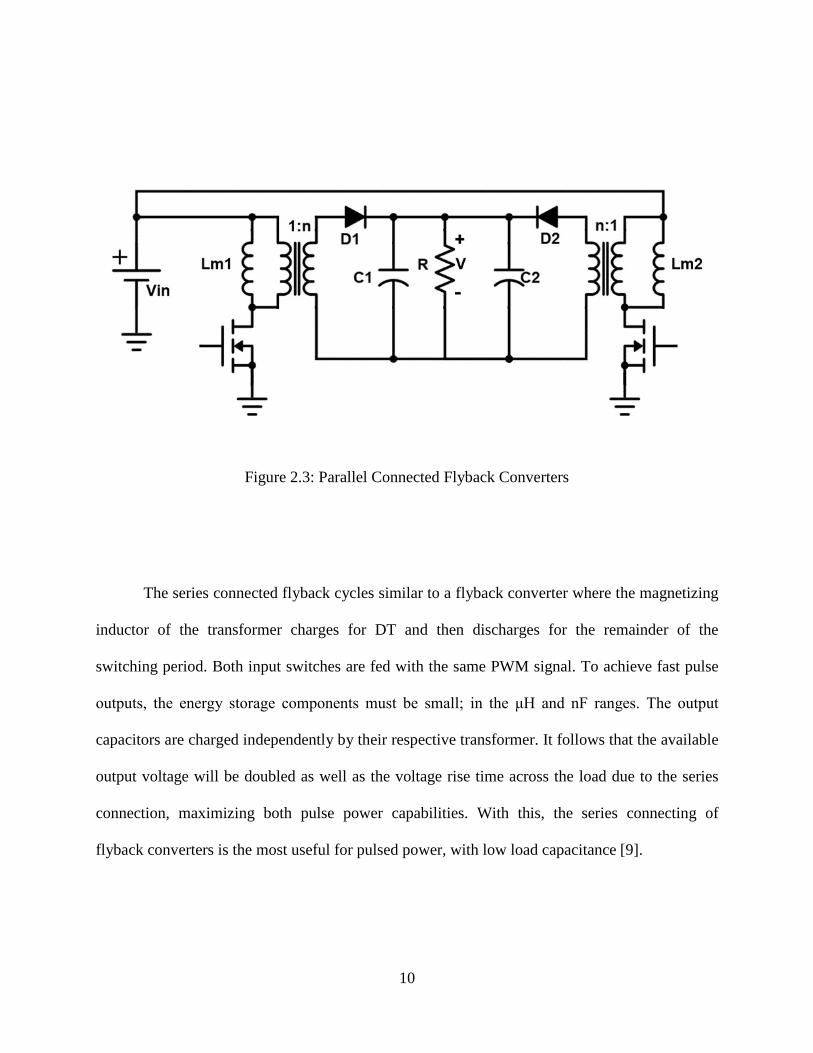
Figure 2.2: Series Connected Flyback Converters
10
Figure 2.3: Parallel Connected Flyback Converters
The series connected flyback cycles similar to a flyback converter where the magnetizing
inductor of the transformer charges for DT and then discharges for the remainder of the
switching period. Both input switches are fed with the same PWM signal. To achieve fast pulse
outputs, the energy storage components must be small; in the μH and nF ranges. The output
capacitors are charged independently by their respective transformer. It follows that the available
output voltage will be doubled as well as the voltage rise time across the load due to the series
connection, maximizing both pulse power capabilities. With this, the series connecting of
flyback converters is the most useful for pulsed power, with low load capacitance [9].

11
3.0 FLYING CAPACITOR MULTILEVEL FLYBACK CONVERTER This section presents the derived operation and characteristics of the FCMFC for the N level
case. The FCMFC combines two existing designs, the flyback and flying capacitor multilevel
(FCML) converters, taking advantage of benefits provided by each to achieve improved peak
output voltage and slew rate. The FCML structure, typically an appendage of buck, boost, and
inverter applications, is realized by cascading multiple output stages of the base converter [7].
The addition of SDC stages (i.e. flying capacitors) creates more operational states and thus
distributes the gain across the stages by a factor of (N - 1) stages. In steady-state operation, the
flying capacitors naturally balance voltage by (kVout) / (N - 1), where k is the stage of interest and
N is the number of converter levels [12]. Dividing the stress amongst multiple stages of the
electronic system lowers the required component voltage ratings and requisite volume [1].

12
3.1 TOPOLOGY DESIGN AND LAYOUT
The novel topology that has been developed utilizes flyback converters and switch-
capacitor-voltage stages (SDC) to maximize voltage output and slew rate (dv/dt). The flying
capacitor multilevel flyback converter (FCMFC) can have M flyback converters in series at the
output, with each flyback having N voltage stages (N-1 SDC stages). Each flyback transformer
has a turns ratio of n. The most basic pulsed power FCMFC, a 2x3 (MxN), is shown in Figure 3.1
with a single SDC stage outlined in red. This MxN layout can be optimized in terms of gain,
stress, and power density for a given application. The follow section will analyze FCMFC to
acquire the considerations for the design process.

13
+ V -
Figure 3.1: Lowest Order FCMFC with a single SDC stage outlined in red
Ll1
Lm1
S1
Ll2 Lm2
Vin
S2
D11 D12
C11 C1o
S11 S12 L O A D
D21 D22
C21 C2o
S21 S22
14
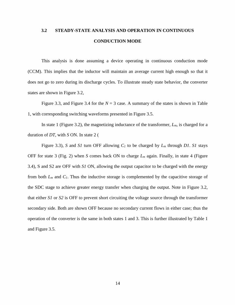
3.2 STEADY-STATE ANALYSIS AND OPERATION IN CONTINUOUS
CONDUCTION MODE
This analysis is done assuming a device operating in continuous conduction mode
(CCM). This implies that the inductor will maintain an average current high enough so that it
does not go to zero during its discharge cycles. To illustrate steady state behavior, the converter
states are shown in Figure 3.2,
Figure 3.3, and Figure 3.4 for the N = 3 case. A summary of the states is shown in Table
1, with corresponding switching waveforms presented in Figure 3.5.
In state 1 (Figure 3.2), the magnetizing inductance of the transformer, Lm, is charged for a
duration of DT, with S ON. In state 2 (
Figure 3.3), S and S1 turn OFF allowing C1 to be charged by Lm through D1. S1 stays
OFF for state 3 (Fig. 2) when S comes back ON to charge Lm again. Finally, in state 4 (Figure
3.4), S and S2 are OFF with S1 ON, allowing the output capacitor to be charged with the energy
from both Lm and C1. Thus the inductive storage is complemented by the capacitive storage of
the SDC stage to achieve greater energy transfer when charging the output. Note in Figure 3.2,
that either S1 or S2 is OFF to prevent short circuiting the voltage source through the transformer
secondary side. Both are shown OFF because no secondary current flows in either case; thus the
operation of the converter is the same in both states 1 and 3. This is further illustrated by Table 1
and Figure 3.5.

15
+ V -
Figure 3.2: States 1 and 3 of FCMFC Operation: Charging Lm
+ V -
Figure 3.3: State 2 of FCMFC Operation: Charging C1
+ V -
Figure 3.4: State 4 of FCMFC Operation: Charging CO
Table 1: Operating Modes of FCMFC (N = 3)
S S1 S2 Operation State 1 1 1 0 Charge Lm State 2 0 0 1 Charge C1 State 3 1 0 1 Charge Lm State 4 0 1 0 Charge Co
Ll D1
V Lm
in
D2 C1 Co
S S1 S2
L O A D
Ll D1 + D2
Vin Lm - C1 Co
S S1 S2
L O A D
Ll D1
V L m
in
+ - C
D2
1 C o
L O A D
S S1 S2

16
Figure 3.5: Switching Diagram FCMFC (N = 3)
Performing a volt-second balance on the magnetizing inductor yields the voltage
conversion ratio for the FCMFC (3.1); the native conversion ratio of the typical flyback
converter with a multiplier of (N-1). This gain equation relates output voltage, V, to input
voltage, Vin, where n is the turns ratio of the transformer. Further detail for this derivation is
provided in Appendix A. This implies that each SDC stage, N, will increase the voltage gain that
the converter can achieve for a given duty cycle, D. Sizing the inductor with (3.2), in terms of
peak-to-peak inductor current ripple ∆IL, is the same as a typical flyback converter, but the ripple
frequency of the inductor is equal to (N-1)fFCMFC, decreasing the required inductor size.
(3.1)

17
- +
C1 + Co
-
L O A D
(3.2)
Figure 3.6 further illustrates the flying capacitor energy multiplication effect. IL /n is the
magnetizing inductor current reflected through the flyback transformer to the secondary side,
that is now being supplemented by the flying capacitor when charging the output stage. For
higher N-level FCMFC converters this would work similarly; building up to the output with extra
charging cycles where every capacitor is charged by Lm and the flying capacitor preceding the
capacitor being charged.
VC1
+
IL/n V
-
Figure 3.6: Output Charging Circuit of FCMFC
Figure 3.7 plots the available gain, (3.1), for the FCMFC for varying N levels. This
details the gain that various N level FCMFCs can achieve for a given duty ratio, with turns ratio
n = 1. The advantage is very significant for D > 0.9 with an N = 11 level converter reaching 190
times the gain for D = 0.95. The minimum range of duty ratio starts at D = 0.7 because FCMFC
requires that D > (N-1)/(N-2) for CCM operation [7]. The gain for a boost converter is also shown
for comparison between FCMFC and the flying capacitor topology in [1].

18
Figure 3.7: Available Gain for FCMFC
Performing a capacitor-charge-balance on the output capacitor yields the inductor current
(3.3), where R is the load resistance. The current will increase by a factor of (N-1) stages. From
ripple current analysis the required inductance equation (3.2) can be found in terms of input
voltage, duty cycle, device frequency, and current ripple. Sizing the inductor with (3.2) is the
same as a typical flyback converter, but similar to the FCML converter, the ripple frequency of
the inductor is equal to (N-1)fFCMFC, decreasing the required inductor size for the same device
frequency. The flying capacitor voltage ripple, ∆VC, and output capacitor voltage ripple, ∆V,
which are derived as (3.4) and (3.5) respectively. They are dependent on the switching
frequency, fFCMFC, because they switch one time for every output cycle.

19
(3.3)
(3.4)
(3.5)

20
3.3 SWITCHING STRESS IN CCM
From Figure 3.1, the switch, S, blocking voltage will be equal to the input voltage and the
secondary side voltage reflected back to the primary. The RMS current through the switch will
equal the inductor current, (3.3), multiplied by the square root of the duty cycle. Therefore, the
input switch stress of a flyback converter can be defined by (3.6), the switch blocking voltage
multiplied by the RMS current that the switch conducts. Similarly, the FCMFC input switching
stress can be defined as (3.7) where the secondary reflected portion of the blocking voltage is
reduced by a factor of the SDC output stages.
(3.6)
(3.7)
(3.8)
If D is held constant when comparing (3.6) to (3.7), the gain would vary between the
FCMFC and the flyback, and the input switch stresses will be the same for the flyback and
FCMFC. This is because the input voltage on the FCMFC can be decreased by N-1 to get the
same output voltage as the flyback. This is not helpful for applications where input voltage is
fixed; therefore it is more useful to compare input switch stress between the flyback and FCMFC
at the same voltage gain, allowing the duty cycle to vary independently. The duty cycles were

21
replaced in (3.6) and (3.7) by solving for D using (3.1). Dividing (3.7) by (3.6) yields (3.8),
where relative stress can be seen varying with gain required by a particular application
(SFCMFC/SFLYBACK = β). This leads to a cumbersome ratio between the input switch stress of
FCMFC and the flyback converter. This equation represents the input switch stress of FCMFC
normalized to that of the standard flyback converter.
Equation (3.8) is plotted in Figure 3.8 for N values from 2 to 11, with 2 being a standard
flyback. For lower gain values there is a peak in the relative stress on each switch and
exponentially decays quickly as the gain increases to suitable application levels. The stress
curves all reach a steady-state value converging to a stress of (N-1) times that of the flyback
converter. The stress increases could prove too much for higher order N converters but are worth
forgoing at lower N due to significant gain increases (Figure 3.7) of the FCMFC. Note that these
results assume no advanced control techniques other than natural PWM behavior with constant
duty cycle.

22
Figure 3.8: FCMFC Input Switch Stress Normalized to Flyback
Figure 3.9 is a plot of the derived switch utilization (3.9) for the FCMFC for various N
cases. This is a ratio of converter load power and total switching stress to show what percent of
the switch stress is being used to transfer power to the output. This is a predictor of switching
losses and semiconductor footprint. The load power is D’VI/n and the total switching stress is the
sum of the input switch, S, stress and the stress of the (N-1) output switches. The standard
utilization function for a flyback converter, (3.10), is plotted as well; as a check for the derived N
level equation. The two match exactly for the N = 2 case as expected. The switch utilization
function for a flyback is poor, with a max of 0.385 at D = 0.33. It’s apparent that adding SDC
stages decreases the overall switch utilization, however, the intended/useful duty cycles for pulse

23
power applications are higher in magnitude (>0.9) where the curves are in steep decline. In this
zone, the utilization function for the flyback is within 5% of the FCMFC relations. Thus the
FCMFC does not suffer significant loss in utilization with added stages. It is also apparent that
the FCMFC will operate at a lower duty cycle than the flyback for a given applications or
voltage gain so the utilization would be higher.
Figure 3.9: FCMFC Switch Utilization for FCMFC Converters
(3.9)
(3.10)
24
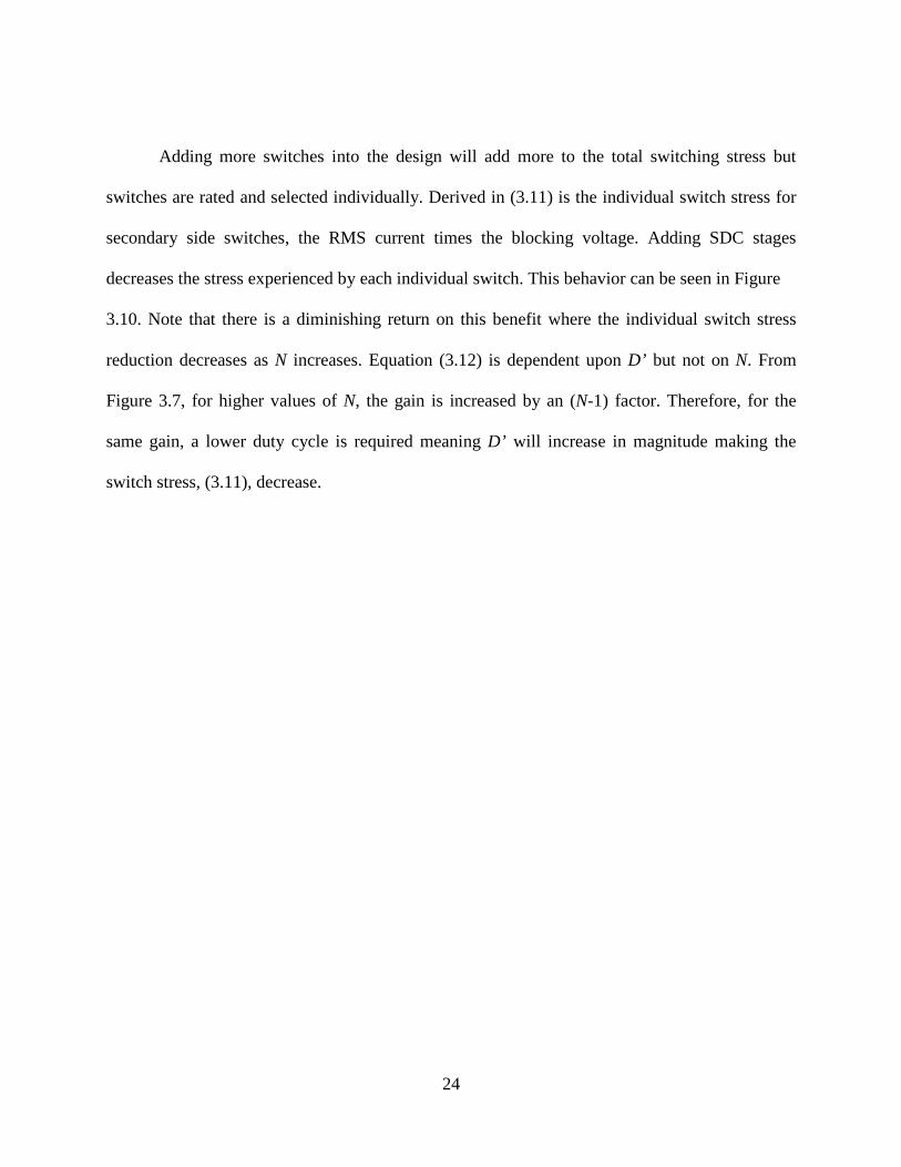
Adding more switches into the design will add more to the total switching stress but
switches are rated and selected individually. Derived in (3.11) is the individual switch stress for
secondary side switches, the RMS current times the blocking voltage. Adding SDC stages
decreases the stress experienced by each individual switch. This behavior can be seen in Figure
3.10. Note that there is a diminishing return on this benefit where the individual switch stress
reduction decreases as N increases. Equation (3.12) is dependent upon D’ but not on N. From
Figure 3.7, for higher values of N, the gain is increased by an (N-1) factor. Therefore, for the
same gain, a lower duty cycle is required meaning D’ will increase in magnitude making the
switch stress, (3.11), decrease.
25
- - N = 3 - - N = 4 - - N = 5 - - N = 6 - - N = 7 - - N = 8 - - N = 9 - - N = 10 - - N = 11
-=- - ----'-- ---L- - --'---- -----'-- ---'- - ----'-- , c ----'----'
Secondary Side Individual Switch Stress 2500 - - - -- - - -- - - -
2000
1500
1000 0 10 20 30 40 50
V/Vin
60 70 80 90 100
Figure 3.10: FCMFC Secondary Side Individual Switch Stress (P = 1kW, n = 10)
(3.11)

26
3.4 INDUCTOR DESIGN
Normalizing the inductance to the N = 2 standard flyback is useful to see how the
required inductor size decreases with increased stages; this is shown by (3.12) and plotted in
Figure 3.11 with n = 1. This ratio of inductor size is found using (3.2) and replacing D with its
equivalent expression based upon (3.1). As the gain approaches infinity, the inductance
approaches a horizontal asymptote at 1/(N-1). Each stage added to the converter will decrease the
required size of the inductor for a given amount of current ripple. This is due in part to the
increased frequency the inductor is switched at in order to charge the (N-1) output stages, the
right half of (3.12); the converters are held to the same output frequency now and not switching
frequency. Also the multiplication effect on the gain contributes to decreasing the required
inductor size, the left half of the ratio. Adding one flying capacitor cuts the required inductance
in half, a significant improvement in terms of power density [16]. Also note that for higher turns
ratios, the curves will approach their asymptotes more slowly, another advantageous finding.
(3.12)

27
Inductance Required by FCMFC normalized to two-level flyback converter. 0. 5 ,1 -----:-------r-----:--= == :::=== r:== N=3 0.45
0.4
0.35
C
::;::::i:;;;;;;;== ----=-----------=---=---=-=i .. - - N = 3
... - - N= 4 · · - - N = 5
- - N = 6 - - N = 7 - - N = 8
ro "g 0 .3
"O C
- - - - - --:-:-:-- -,- - N = 9 - - N = 10
.. - - N = 11
0.25 Q)
r-o 0 .2 .E...
0z 0 . 15
0 . 1
0.05
N =: t J
o - - -- - ---- -- - -- - 0 10 20 30 40 50
V/Vin 60 70 80 90 100
Figure 3.11: Required Magnetizing Inductance Normalized to Flyback Design

28
3.5 PULSED POWER OPERATION AND ANALYSIS IN DISCONTINUOUS
CONDUCTION MODE
The charging modes for CCM shown in Figure 3.2,
Figure 3.3, and Figure 3.4 for a single flyback FCMFC, are the same for DCM mode,
with the only difference being that the inductor fully discharges when expelling its energy to the
secondary side capacitors. The magnetizing inductor current can be calculated as,
(3.13)
where Lm is the magnetizing inductance and Ts is the switching period. The peak current equates
to a peak inductor energy that is completely discharged into the flying capacitor, (3.14). The
inductor will charge again and then release all of its energy into the next flying capacitor. This
energy will be bolstered by that of the first flying capacitor as shown in Figure 3.4, (3.15). For
the general case of N-1 capacitors, the inductor energy will be passed to the output N-1 times,
building up the voltage incrementally across the flying capacitors. Solving (3.15) and
generalizing for the (N-1) level case, yields an equation for the output voltage pulse peak for a
single FCMFC (3.17), with all capacitors equal in size.
(3.14)
= (3.15)

29
(3.16)
Multiple flybacks, as inFigure 3.1, of an FCMFC will function independently, where the
magnetizing inductor of the transformer charges for DT and then discharges for the remainder of
the switching period. All input switches are fed with the same PWM signal for synchronization.
The output capacitors are charged independently by their respective transformer magnetizing
inductance. It follows that the available output voltage will be increased by a factor of the
number of flybacks that are connected in series across the load, M. The voltage rise time will
also increase by this factor, maximizing both pulsed power characteristics. Appending (3.16)
with this M factor, and also inserting the expression for the peak magnetizing current, (3.13),
yields a comprehensive equation to shape voltage pulses of the FCMFC listed as (3.17).
(3.17)
Flying capacitors increase gain by a root factor, , and connecting M flybacks in
series has additional voltage gain benefit. To achieve fast pulse outputs, the energy storage
components must be small; in the μH and nF ranges.
The rate of voltage rise, or slew rate, across a single output capacitor is proportional to
the current through it, (3.18). The current, Im, is provided by the magnetizing inductance,
assuming high load resistance, Figure 3.4. With M flybacks connected at the output, there are M
voltage rises added together across the load allowing for a total slew rate defined by (3.19).

30
(3.18)
(3.19)
(3.18) is the rate of voltage rise for an individual output capacitor while (3.19) represents
the slew rate across the load, which is the summation of all (M) the output capacitors voltages.
31
4.0 RESULTS AND DISCUSSION The nature of this work brings about two types of results. Because it is a new topology with new
characteristic equations there are results that prove the equations through multiple device
iterations. This is mainly proving the benefits of adding the switching (SDC) stages at the output.
The second type of result is used to prove the merit of this converter topology. Existing devices
in the literature have been benchmarked and the FCMFC is optimized to perform at or above the
levels of the devices in the literature. FCMFC performs at the levels of existing structures while
utilizing fewer devices in its design.

32
4.1 DC-DC STEADY-STATE RESULTS
4.1.1 Proving the Newly Found Conversion Ratio
To validate the derived converter behavior, steady-state DC-DC implementations of the
FCMFC were developed in Simulink/PLECS. Table 2 shows the component values and shows
the steady state voltage output for three different cases: N = 2, 3, and 4. The average voltage and
ripple values were compared to the expected values from the derived equations and are shown in
Table III. For the same set of electrical parameters, the results show that the FCMFC scales the
output by a multiple of its SDC stages, when compared to the standard flyback converter
conversion ratio - (3) with N = 2. Notice that the output frequency is decreased by the same
multiple because of the added charging states. This is because the switching frequency (fs) was
held constant, and no the device frequency (fFCMFC). With a fixed capacitance for all flying
capacitors, the output ripple scales with the output voltage, as reflected in Table 3. Similar to the
flyback converter, the voltage ripple can be decreased for a fixed capacitance by increasing
fFCMFC, as shown in (3.5).
Table 2: Steady-State DC-DC Step-Up FCMFC Converter Parameters
Capacitors LM Vin fs D R n 0.825μF 152μH 10V 72kHz 0.15 250Ω 10

33
Figure 4.1: FCMFC Steady-State DC-DC Step-Up Results
Table 3: Output Voltage Average and Ripple Values for Various FCMFC Converter Architectures
N-1 V Expected (3) ΔV Expected (7) 1 17.55 17.65 0.177 0.178 2 35.03 35.29 2.71 2.73 3 52.44 52.94 7.57 7.66
34
4.1.2 Optimizing to 7-Level FCML
The topology design of [1] is derived from a boost converter that is adapted with flying
capacitors to increase efficiency and power density. It is a 7-level converter consisting of six
SDC cells controlled with PWM and shown in Figure 2.1. The input voltage was 100V with an
output of 1000V resulting in a gain of 10. Using the same device frequency of 72kHz, and
passive component sizes, the FCMFC can be adapted to this application using (3.1) with a D =
0.769. This results in a 4-level (N = 4) converter consisting of three SDCs; similar to Figure 3.2
but with one additional SDC stage.
The turns ratio is kept at 1 to more directly compare the benefit of the flying capacitors
between the boost FCML converter and the proposed FCMFC. Both of the converters were
simulated in PLECS to compare their natural performance with static PWM. Simulation results
are shown in Table 4 and Figure 4.2.
Table 4: DC-DC Boosting Simulation Results
Converter Vavg Vripple FCML Boost [1] 994.5 V 12.4 V
FCMFC 994.5 V 12.8 V

35
Figure 4.2: DC-DC Boosting Simulation Results
The FCMFC is yields the same average DC voltage output as the FCML boost. The
ripple of the FCMFC is only 0.4V higher than that of the FCML boost, a negligible difference.
This comparison is to show that the FCMFC can perform similarly to an existing topology in the
literature with 2 less switches, and half of the diodes, and capacitors required on the output stage,
as shown in Table 5. Note that the voltage gain could be increased significantly if the turns ratio
was greater than 1.
Table 5: DC-DC Boosting Required Components
Converter Switches Diodes Capacitors FCML Boost [1] 6 6 6
FCMFC 4 3 3

36
4.2 PULSED POWER RESULTS
4.2.1 Preliminary Pulsed Power Results
As presented previously, the benefits of flying capacitor topologies and combining
converters in series offer significant advantages to warrant their combination for pulsed power.
Figure 3.1 shows the proposed FCMFC in a series configuration for pulsed power applications.
DCM operation is used here due to the pulse nature of the output voltage required. This also
allows for maximum energy transfer because the inductor current reaches zero when discharging
into flying capacitors. Both the upper and lower converters within the structure function in
unison to provide high voltage peaks to the load. There are also diodes added to the phase leg of
the secondary side of the transformer to prevent reverse current while charging the magnetizing
inductor. Similar to the single FCMFC, this series configuration was simulated in PLECS to
demonstrate operation. The converter was sized to match that of the case in [9] and parameters
are shown in Table 6. The converter is defined by the number of voltage levels, N, for a given
FCMFC, and by the number of series connected converters, M. This makes for MxN possible
configurations. A 3x2 configuration is shown in Figure 3.1.
Table 6: Component Values for FCMFC (3x2)
Capacitors LM Ll Vin fs D R 2.35μF 152μH 1.6μH 17V 1kHz 0.15 20kΩ

37
The simulation produces 10kV pulses with a 1201V/μs rise time. These results were
compared to those obtained from single level (M = 1) FCMFC configurations and the series
flyback converter from [9], as shown in Table V.
Table 7: Simulation Results for Variations of Pulsed Power Topologies
Description Vlevels (N)
Series (M) Pulse Voltage dv/dt
Series Flyback Stacked (2x2) [9] 2 2 7.0Kv 816V/μs
SERIES FCMFC (3x2) 3 2 10Kv 1201V/μs
FCMFC (3x1) 3 1 5.5Kv 618V/μs
FCMFC (4x1) 4 1 6.7Kv 705V/μs
Figure 4.3: FCMFC (3x2) Pulsed Power Waveforms
Comparing the series FCMFC (row 2) to the series flyback (row 1), it can be seen that for
a converter of similar architecture, the FCMFC achieves 43% higher output voltage and 47%
faster slew rate. Additionally, the (4x1) FCMFC achieves 96% of the peak voltage and 86% of
the slew rate, while the (3x1) FCMFC reaches 79% and 76%, respectively, compared to the

38
series flyback stacked case. Figure 4.3 shows the 10kV pulse and also the voltage levels on the
two flying capacitors. It can therefore be seen that for an equivalent converter size, the series
FCMFC drastically outperforms the series flyback configuration. Additionally, if size is the chief
concern, the single level FCMFC can be used to achieve similar performance to the series
flyback with significantly reduced converter mass and volume. The FCMFC can be further
scaled to the requisite pulsed-power application through increasing the SDC capacitance when
allowed by the application or by adding additional SDC stages.
4.2.2 Optimizing to 10-level Series Flyback Converter
A hardware implementation consisting of 10 flyback converters connected in series at the
output achieved a 20.8kV pulse with 8kV/μs rise time [9]. This converter was simulated in
PLECS for comparison to the FCMFC. Both converters were constrained by the specifications of
the hardware implementation: D = 0.10, fs = 1kHz, Vin = 10V, and the same passive components.
Using (3.17) the FCMFC can be optimized to produce the same voltage peak with M = 5 and N =
5, five series flybacks, each with 4 SDC stages, as shown in Figure 4.4, with results in Table 8
The voltage pulses are shown in Figure 4.5. The FCMFC is able to achieve a 1kV higher
pulse and only 700V/μs slower slew rate. It can achieve these results while having half of the
flybacks of the 10-level from the literature. This also results in the FCMFC drawing half of the
source current, lowering the stress on the input voltage source. Note that the FCMFC will have a
repetition rate that is (N-1) times slower than its counterpart. This is because the switching
frequencies are forced to be the same for the comparison. The switching frequency could be
increased along with altering component sizes to achieve a 1 kHz repetition rate at the same
pulse performance.

39
+ V -
Figure 4.4: 5x5 FCMFC for Pulsed Power
Table 8: Pulsed Power Simulation Results
Converter Voltage Peak Slew Rate (dv/dt) Flyback [4] 35kV 8.7kV/μs
FCMFC 36kV 8.0kV/μs
Ll1
Lm1 Co1
S S1 S2 S3 S4
Ll2
Lm2 Co2
S S1 S2 S3 S4
Ll3
Lm3 Co3
S S1 S2 S3 S4
Ll4
Lm4 Co4
S S1 S2 S3 S4
Ll5
Lm5 Co5
Vin
S S1 S2 S3 S4
L O A D

40
."..,' >
Time (s) 5x5 FCMFC
."..,' 0 >
I I
1.515 1.520 Time (s)
I
1.525 x le-2
Figure 4.5 FCMFC vs Flyback Voltage Pulses
10 Flybacks in Series [10]
I I
1.510 1.515 1.520 1.525 x le-2
0
1.5'10

41
5.0 CONCLUSIONS AND FUTURE WORK The contribution of this work is a new power electronic converter topology referred to as the
FCMFC that utilizes both the flyback converter architecture for isolation and SDC stages
associated with the flying capacitor multilevel converter. The FCMFC achieves a voltage
conversion ratio scaled by (N-1) DC-DC steady-state (CCM) operation, as compared to the
standard flyback topology. Specifically, adding flying capacitors to the flyback converter
architecture increases the available gain by a multiple of the capacitors added, for the same
operating parameters. The gain benefits are also seen for pulsed power (DCM) operation. Adding
the SDC stage to a series FCMFC yielded a 3kV increase in voltage pulse peak with a 385V/μs
rise time net change compared to the latest series structures in the literature. Results also show
that for steady state operation, the system gain of the FCMFC can be doubled or tripled by
adding one or two flying capacitors. For both applications the switching stresses will decrease by
distributing the net gain across multiple SDC stages with magnetic reduction benefits.
The FCMFC is a new topology that shows great promise for DC-DC boosting and pulsed
power applications. This topology benefits from lower magnetic component size with increased
available gain, making it viable for high power density applications. The gain can be doubled for
half of the required magnetic components as per equations (3.1) and (3.12). The converter is able
to perform within the same application space, steady-state boosting, as an existing topology with
half of the SDC stages. For pulsed power the FCMFC outperforms an existing structure in peak

42
voltage pulse while only requiring half of the flyback converters. It does this by adding three
SDC stages at the output. The FCMFC can do this with half of the current load on the input
power source with no increase in stress on the input switches of the constituent converters.
The logical next step for this research is to design and build a version of the FCMFC. This
will require the development of a control scheme that is aimed at a specific application. Some
concerns for the control are voltage balancing of the capacitor stages and these are outlined in
Appendix B.
Another interesting route that can be explored is using the FCMFC in CCM operation for
pulsed power. This idea is further explored in Appendix C.

43
APPENDIX A
DUTY RATIO DERIVATION THROUGH INDUCTOR VOLT-SECOND BALANCE This is a detailed derivation of equation 3.1. The input switch is the main switch in the flyback
topology and thus must be the primary driver when deriving equations. Using other switches
results in a loss of information and thus incorrect equations. The secondary side switches are
added to the flyback structure and are there to cycle the flying capacitors correctly. The volt-
second balance of the inductor using TFCMFC for the general (N - 1) level case is as follows:
(3.1)

44
APPENDIX B
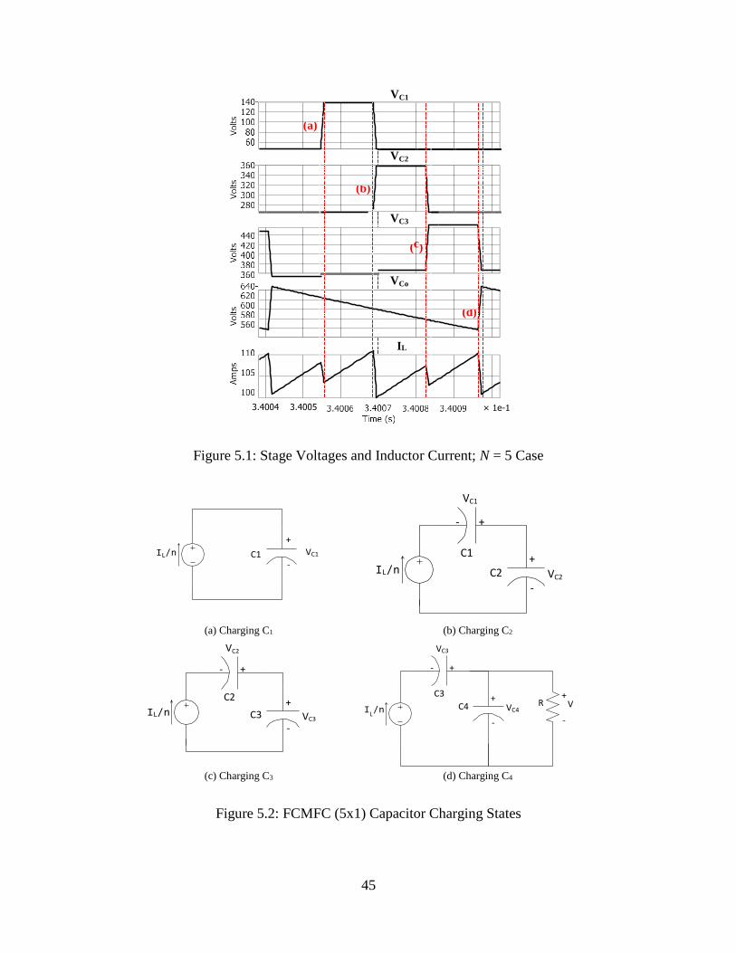
N = 5 CASE TO ILLUSTRATE CHARGING STATES For the N = 5 case, the converter’s state waveforms are presented in Figure 5.1. Here it can be
seen that the capacitor ripple values match those predicted by (3.5). Figure 5.2 shows the four
capacitor charging states which correspond to their respective time interval in Figure 5.1. Note
that IL /n is the magnetizing inductor current, reflected through the flyback transformer to the
secondary side. Also note that the intermediate state of charging the magnetizing inductor is not
considered here. In between every capacitor charging state the inductor will be charged again
using the input voltage source, as per the CCM steady-state operation described previously. This
appendix is concerned with the SDC stage voltages at steady-state and how they affect inductor
current.
45
VC1
c
(a)
VC2 (b)
VC3
( )
VCo
(d)
IL
Figure 5.1: Stage Voltages and Inductor Current; N = 5 Case
+ IL/n C1 VC1
-
VC1
- +
C1 + IL/n C2 VC2
-
(a) Charging C1
(b) Charging C2 VC2
- +
C2 + IL/n C3 VC3
-
VC3
- +
C3 + +
I /n C4 VC4 R V L
- -
(c) Charging C3 (d) Charging C4
Figure 5.2: FCMFC (5x1) Capacitor Charging States

46
By analyzing the charging stages of the FCMFC, the inductor balance and reset can be
shown. During the charging of C1, shown in Figure 5.2a, only C1 is seen by the transformer.
During the next interval, shown in Figure 5.2b, the inductor charges C2 with the assistance of
C1. Comparing the slope of IL from state (a) to state (b), it can be seen that the effective change
in capacitance has been seen by the inductor. These two states reset the inductor, balancing IL.
For a typical two stage converter, such as the flyback, charging the inductor increases the current
which must then be equally decreased on the discharge cycle in order to maintain magnetizing
current stability. By adding three stages, the converter adds six more charging states (three more
to charge the inductor and three more to charge the added stages). In pulsed power applications,
effects of the IL oscillations will not be critical; conversely, in steady-state DC-DC applications
harmonics could damage the converter load. The ramifications of this behavior will be important
when a hardware implementation of this device will be designed. A control scheme will force
stage balancing as desired by the application.

47
APPENDIX C
AVAILABLE ENERGY FOR POWER PULSE IN CCM The power pulse is typically described in terms of the energy that it provides [8, 9]. This
appendix derives a plot to illustrate how the FCMFC increases available pulse energy as a
function of the number of SDC stages. Some pulsed power converters operate in CCM mode and
use an output switch the deliver the power pulse [4]. This is advantageous for FCMFC because
the voltage gain benefit of SDC stage is greater in CCM than in DCM: (N-1) vs
respectively (as per 3.1 and 3.17). With this it makes sense to do a CCM analysis where output
energy is the focus.
(B.1)
(B.2)
(B.3)

48
Equation (B.1) is the available output power of the FCMFC; using this leads to (B.2) and
(B.3), energy available in the inductor and output capacitor for various cases. B.2 specifically
can be used to design a pulsed power converter where a certain energy pulse is required. Figure
5.3 is a plot for varying N level FCMFCs of how much energy will be available for a power
pulse. A dashed red line is overlaid to make a proper comparison between levels. This line shows
the operating points that a converter would be at because of the increased voltage gain provided
by the added SDC stages. There is an exponential increase in available energy for adding SDC
stages. This makes a CCM FCMFC attractive for pulsed power conversion.
Figure 5.3: Energy Available for Power Pulse of FCMFC

49
BIBLIOGRAPHY [1] Z. Liao, Y. Lei, R. C. N. Pilawa-podgurski, and N. W. Street, “A GaN-based Flying-
Capacitor Multilevel Boost Converter for High Step-up Conversion,” 2016. [2] J. C. Martin, “Nanosecond Pulse Techniques,” Proc. IEEE, vol. 80, no. 6, pp. 934–945,
1992. [3] E. Schamiloglu, R. J. Barker, M. Gundersen, and A. A. Neuber, “Scanning the
technology: Modern pulsed power: Charlie Martin and Beyond,” Proc. IEEE, vol. 92, no. 7, pp. 1014–1019, 2004.
[4] A. Elserougi, A. M. Massoud, A. M. Ibrahim, and S. Ahmed, “A high voltage pulse-
generator based on DC-to-DC converters and capacitor-diode voltage multipliers for water treatment applications,” IEEE Trans. Dielectr. Electr. Insul., vol. 22, no. 6, pp. 3290– 3298, 2015.
[5] H. Akiyama, T. Sakugawa, T. Namihira, K. Takaki, Y. Minamitani, and N. Shimomura,
“Industrial applications of pulsed power technology,” IEEE Trans. Dielectr. Electr. Insul., vol. 14, no. 5, pp. 1051–1064, 2007.
[6] K. Yamashita, T. Hatanaka, H. Akiyama, and T. Sakugawa, “Study of fast rise time pulse
power generator using SiC-MOSFET and FRD,” Pulsed Power Conf. (PPC), 2015 IEEE, pp. 1–4, 2015.
[7] N. Pallo et al., “Power-Dense Multilevel Inverter Module using Interleaved GaN-Based
Phases for Electric Aircraft Propulsion,” Apec 2018, pp. 1656–1661, 2018. [8] S. Zabihi, F. Zare, G. Ledwich, A. Ghosh, and H. Akiyama, “A new pulsed power supply
topology based on positive buck-boost converters concept,” IEEE Trans. Dielectr. Electr. Insul., vol. 17, no. 6, pp. 1901–1911, 2010.
[9] P. Davari, F. Zare, and A. Ghosh, “High-Votlage Modular Power Supply Using Parallel
and series configurations of flyback converter for pulsed power applications,” IEEE Trans. PLASMA Sci. VOL. 40, NO. 10, Oct. 2012, vol. 40, no. 10, pp. 1517–1522, 2012.
[10] T. Heeren, T. Ueno, D. Wang, T. Namihira, S. Katsuki, and H. Akiyama, “Novel Dual
Marx Generator for Microplasma Applications,” IEEE Trans. Plasma Sci., vol. 33, no. 4, pp. 1205–1209, 2005.

50
[11] F. Wang, A. Kuthi, C. Jiang, Q. Zhou, and M. Gundersen, “Flyback Resonant Charger for High Repetition Rate J-T,” pp. 85–88.
[12] Z. Ye, Y. Lei, and R. C. N. Pilawa-podgurski, “A Resonant Switched Capacitor Based 4-
to-1 Bus Converter Achieving 2180 W/in3 Power Density and 98.9% Peak Efficiency,” Apec 2018, pp. 121–126, 2018.
[13] M. Khazraei, H. Sepahvand, K. Corzine, and M. Ferdowsi, “A generalized capacitor
voltage balancing scheme for flying capacitor multilevel converters,” Conf. Proc. - IEEE Appl. Power Electron. Conf. Expo. - APEC, pp. 58–62, 2010.
[14] Z. Ye, Y. Lei, Z. Liao, and R. C. N. Pilawa-Podgurski, “Investigation of capacitor voltage
balancing in practical implementations of flying capacitor multilevel converters,” 2017 IEEE 18th Work. Control Model. Power Electron. COMPEL 2017, 2017.
[15] C. B. Barth et al., “Design and control of a GaN-based, 13-level, flying capacitor
multilevel inverter,” 2016 IEEE 17th Work. Control Model. Power Electron. COMPEL 2016, 2016.
[16] Y. Lei, W.-C. Liu, and R. C. N. Pilawa-Podgurski, “An Analytical Method to Evaluate
and Design Hybrid Switched-Capacitor and Multilevel Converters,” IEEE Trans. Power Electron., vol. 8993, no. c, pp. 1–1, 2017.
![A Review On Various Multilevel Inverter Topologiesgjar.org/publishpaper/vol2issue1/d98r17.pdf · flying capacitor multilevel inverter and converter. Ryan et al [38] introduces a control](https://static.fdocuments.net/doc/165x107/5f0b58f67e708231d43011a6/a-review-on-various-multilevel-inverter-flying-capacitor-multilevel-inverter-and.jpg)


![Catalogue FLYBACK Equivalent - [PDF Document] FLYBACK Equivalent FlyBack Equivalent flyback reemplazo conversor Flyback tv fly-back Flyback Tester Flyback Converter conversor Flyback](https://static.fdocuments.net/doc/165x107/5a832a447f8b9a9d308e9416/catalogue-flyback-equivalent-pdf-document-flyback-equivalent-flyback-equivalent.jpg)