Adaptive Object Representation with Hierarchically-Distributed ...

University of Tennessee, KnoxvilleTrace: Tennessee Research and CreativeExchange
Doctoral Dissertations Graduate School
12-2010
Adaptive Voltage Control Methods usingDistributed Energy ResourcesHuijuan LiUniversity of Tennessee - Knoxville, [email protected]
This Dissertation is brought to you for free and open access by the Graduate School at Trace: Tennessee Research and Creative Exchange. It has beenaccepted for inclusion in Doctoral Dissertations by an authorized administrator of Trace: Tennessee Research and Creative Exchange. For moreinformation, please contact [email protected].
Recommended CitationLi, Huijuan, "Adaptive Voltage Control Methods using Distributed Energy Resources. " PhD diss., University of Tennessee, 2010.http://trace.tennessee.edu/utk_graddiss/894

To the Graduate Council:
I am submitting herewith a dissertation written by Huijuan Li entitled "Adaptive Voltage ControlMethods using Distributed Energy Resources." I have examined the final electronic copy of thisdissertation for form and content and recommend that it be accepted in partial fulfillment of therequirements for the degree of Doctor of Philosophy, with a major in Electrical Engineering.
Fangxing Li, Major Professor
We have read this dissertation and recommend its acceptance:
Kevin Tomsovic, Yilu Liu, Xueping Li
Accepted for the Council:Carolyn R. Hodges
Vice Provost and Dean of the Graduate School
(Original signatures are on file with official student records.)

To the Graduate Council:
I am submitting herewith a dissertation written by Huijuan Li entitled “Adaptive Voltage Control
Methods using Distributed Energy Resources.” I have examined the final electronic copy of this
dissertation for form and content and recommend that it be accepted in partial fulfillment of the
requirements for the degree of Doctor of Philosophy, with a major in Electrical Engineering.
Fangxing (Fran) Li , Major Professor
We have read this dissertation
and recommend its acceptance:
Kevin Tomsovic
Yilu Liu
Xueping Li
Accepted for the Council:
Carolyn R. Hodges
Vice Provost and Dean of the Graduate School
(Original signatures are on file with official student records.)

Adaptive Voltage Control Methods using Distributed Energy
Resources
A Dissertation Presented for the
Doctor of Philosophy Degree
The University of Tennessee, Knoxville
Huijuan Li
December 2010

ii
Acknowledgements
I would like to thank my advisor, Dr. Fangxing (Fran) Li, for his continuous guidance
and support not only in my doctoral study, but also in student life. His dedication in teaching,
tutoring, and assistance to me is greatly appreciated.
I am very thankful to Dr. Yan Xu at Oak Ridge National Laboratory (ORNL) for her
inspirational instructions and work on the experiment. I also thank Mr. D. Tom Rizy and Mr.
John D. Kueck at Oak Ridge National Laboratory for their advice and help. In particular, the
field experiment at ORNL presented in subsection 4.5 (Pages 51-55) was mainly performed by
ORNL researchers including Dr. Yan Xu and Mr. Tom Rizy. The field experiment results are
included in this dissertation for completeness.
I am also thankful to all the professors and students in the UT EECS Power Lab,
including those already graduated. Your friendship, encouragement, and help were indeed
beneficial to my studies and research work. In addition, I am very thankful to Dr. Kevin
Tomsovic, Dr. Yilu Liu and Dr. Xueping Li, for their time and effort in serving as my committee
members.
Finally, I would like to express my appreciation and love to my husband, Yong Yin, and
my parents, En Li and Zhilan Zhou. They have always loved me, supported me, and encouraged
me unconditionally.

iii
Abstract
Distributed energy resources (DE) with power electronics interfaces and logic control
using local measurements are capable of providing reactive power related to ancillary system
services. In particular, local voltage regulation has drawn much attention in regards to power
system reliability and voltage stability, especially from past major cascading outages. This
dissertation addresses the challenges of controlling the DEs to regulate the local voltage in
distribution systems.
First, an adaptive voltage control method has been proposed to dynamically modify the
control parameters of a single DE to respond to system changes such that the ideal response can
be achieved. Theoretical analysis shows that a corresponding formulation of the dynamic control
parameters exists; hence, the adaptive control method is theoretically solid. Also, the field
experiment test results at the Distributed Energy Communications and Controls (DECC)
Laboratory in single DE regulation case confirm the effectiveness of this method.
Then, control methods have been discussed in the case of multiple DEs regulating
voltages considering the availability of communications among all the DEs. When
communications are readily available, a method is proposed to directly calculate the needed
adaptive change of the DE control parameters in order to achieve the ideal response. When there
is no communication available, an approach to adaptively and incrementally adjust the control
parameters based on the local voltage changes is proposed. Since the impact from other DEs is
implicitly considered in this approach, multiple DEs can collectively regulate voltages closely
following the ideal response curve. Simulation results show that each method, with or without
communications, can satisfy the fast response requirement for operational use without causing

iv
oscillation, inefficiency or system equipment interference, although the case with communication
can perform even faster and more accurate.
Since the proposed adaptive voltage regulation method in the case of multiple DEs
without communication, has a high tolerance to real-time data shortage and can still provide
good enough performance, it is more suitable for broad utility applications. The approach of
multiple DEs with communication can be considered as a high-end solution, which gives faster
and more precise results at a higher cost.

v
Table of Contents
1 Introduction ......................................................................................................................... 1
1.1. Background ................................................................................................................ 1
1.1.1. Development of Distributed Energy Resources ......................................................... 1
1.1.2. Types of Distributed Energy Resources .................................................................... 3
1.1.3. Interconnection to Grid .............................................................................................. 5
1.1.4. Voltage Regulation by DE with PE Interface ............................................................ 7
1.2. Motivation ................................................................................................................ 11
1.3. Dissertation Outline ................................................................................................. 13
1.4. Summary of Contributions ....................................................................................... 14
2 Literature Review.............................................................................................................. 16
2.1. Chapter Introduction ................................................................................................ 16
2.2. Voltage Control in Distribution Systems with DEs ................................................. 16
2.3. PE interfaces Design to Implement Voltage Regulation ......................................... 21
2.4. Scope of this Work................................................................................................... 23
3 Challenges of the Control Parameters for Voltage-Regulating Distributed Energy Resources ...................................................................................................................................... 24
3.1. Chapter Introduction ................................................................................................ 24
3.2. Factors Affecting Dynamic Performance of Controller for Voltage Control .......... 24
3.3. Simulations on Voltage Control with PE Interfaced DE ......................................... 26
3.3.1. Impact of KP and KI on Voltage Regulation ........................................................... 26
3.3.2. Impact of DE Location on Voltage Regulation ....................................................... 30
3.3.3. Impact of Loading Level on Voltage Regulation .................................................... 32
3.4. Chapter Summary and Discussion ........................................................................... 35
4 Adaptive Voltage Control with a Single DE..................................................................... 36
4.1. Chapter Introduction ................................................................................................ 36
4.2. Implementation of Adaptive Method for DE Controller ......................................... 36
4.2.1. Determine the DC Source Voltage .......................................................................... 36
4.2.2. Set the Initial PI Controller Gains ............................................................................ 38
4.2.3. Adaptively Adjusting the PI Controller Gain Parameters........................................ 40
4.3. Analytical Formulation of the Adaptive Method ..................................................... 42
4.4. Simulation Results ................................................................................................... 50
4.5. Field Experiment Results at ORNL ......................................................................... 55
4.6. Chapter Conclusion .................................................................................................. 60
5. Voltage Regulation with Multiple DEs............................................................................. 61
5.1. Chapter Introduction ................................................................................................ 61
5.2. Challenges in Voltage Control with Multiple DEs .................................................. 61
5.3. Theoretical Formulation of the Parameters for Multiple Voltage-Regulating DEs
with Adaptive Control Method ................................................................................................. 68
5.4. Voltage Regulation with Communication ............................................................... 78
5.5. Voltage Regulation without Communication .......................................................... 98
5.6. Chapter Conclusion ................................................................................................ 112
6. Conclusions and Future Work ........................................................................................ 114

vi
6.1. Dissertation Conclusion ......................................................................................... 114
6.2. Future Work ........................................................................................................... 116
List of References ....................................................................................................................... 118
Publications during Ph.D. Study ................................................................................................. 126
Award .......................................................................................................................................... 128
Vita .............................................................................................................................................. 129

vii
List of Figures
Figure 1.1. Distributed energy resources reshaping the traditional grid [1]. .................................. 2
Figure 1.2. Interconnection Interfaces of DE with Power Systems. ............................................... 7
Figure 1.3. Parallel connection of a DE with PE converter. ........................................................... 9
Figure 1.4. Control diagram for voltage regulation. ..................................................................... 10
Figure 3.1. Simplified model of the distribution system with multiple controllable DEs interfaced
to it. ....................................................................................................................................... 25
Figure 3.2. Single line diagram of the distribution system with DEs. .......................................... 27
Figure 3.3. Voltage regulation with different control parameters-single DE case. ...................... 27
Figure 3.4. Voltage regulation with different control parameters-two DEs case. ........................ 29
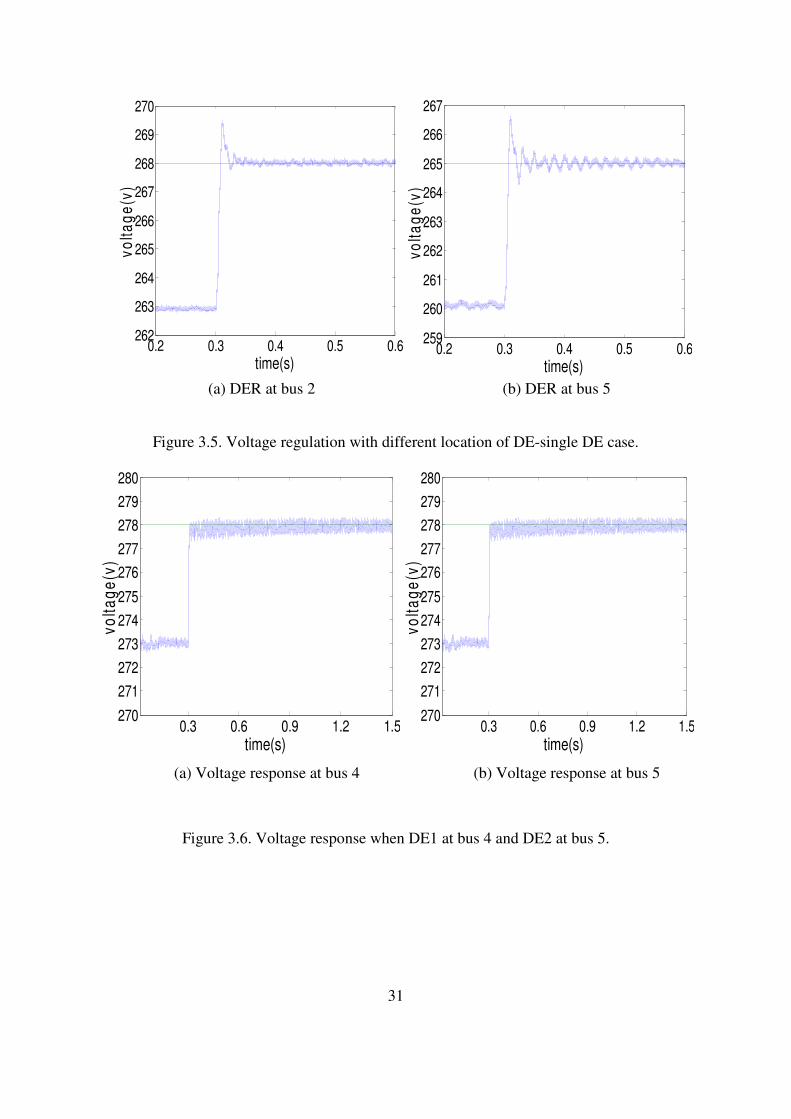
Figure 3.5. Voltage regulation with different location of DE-single DE case. ............................. 31
Figure 3.6. Voltage response when DE1 at bus 4 and DE2 at bus 5. ........................................... 31
Figure 3.7. Voltage response when DE1 at bus 2 and DE2 at bus 5. ........................................... 32
Figure 3.8. Voltage responses with different amount of load-single DE case. ............................. 33
Figure 3.9. Voltage responses when load at bus 3 is 13.6kW+2.1kVar. ...................................... 34
Figure 3.10. Voltage responses when load at bus 3 is 27.2kW+2.1kVar. .................................... 34
Figure 4.1. PWM voltage control by varying modulation index ma. ............................................ 37
Figure 4.2. Adaptive Control of the Voltage Regulation. ............................................................. 41
Figure 4.3. The desired and actual response of the controller. ..................................................... 42
Figure 4.4. A schematic diagram of a network and sources. ........................................................ 43
Figure 4.5. A radial test system. .................................................................................................. 47
Figure 4.6. Comparison of the value of KP generated by the two methods. ................................ 48
Figure 4.7. Comparison of the value of KI generated by the two methods. ................................. 49
Figure 4.8. Tracking ideal response by adjusting KP and KI with the two methods. .................... 49
Figure 4.9. Voltage regulation with adaptive adjustment of KP and KI. ....................................... 53
Figure 4.10. Comparing the desired and actual voltage deviations. ............................................. 53
Figure 4.11. Real power injection. ................................................................................................ 54
Figure 4.12. Reactive power injection. ......................................................................................... 54
Figure 4.13. Non-adaptive voltage regulation with KP and KI fixed at the initial values. ............ 55
Figure 4.14. ORNL’s DECC Laboratory. ..................................................................................... 57
Figure 4.15. PCC voltage at the inverter without voltage regulation. .......................................... 58
Figure 4.16. PCC voltage (in RMS) with non-adaptive voltage regulation. ................................ 58
Figure 4.17. PCC voltage (in RMS) with adaptive voltage regulation. ........................................ 59
Figure 4.18. Comparison of the desired and actual voltage deviations. ....................................... 60
Figure 5.1. A radial test system installed with two DEs. .............................................................. 63
Figure 5.2. Voltage responses of DE2 in Scenarios 1, 2, and 3. ................................................... 64
Figure 5.3. Voltage regulation of DE1 in Scenario 2. .................................................................. 64
Figure 5.4. Voltage regulation of DE1 in Scenario 3. .................................................................. 65
Figure 5.5. Voltage response of DE2 in scenario 4 and scenario 5. ............................................. 67
Figure 5.6. A schematic diagram of a network and with multiple DE sources. ........................... 69
Figure 5.7. Terminal voltage of DE1 - Scenario 5. ....................................................................... 74
Figure 5.8. Terminal voltage of DE2 – Scenario 5. ...................................................................... 75

viii
Figure 5.9. The calculated value of KP of DE1 in adaptive control - Scenario 5. ......................... 75
Figure 5.10. The calculated value of KI of DE1 in adaptive control - Scenario 5. ....................... 76
Figure 5.11. The calculated value of KP of DE2 in adaptive control - Scenario 5. ....................... 76
Figure 5.12. The calculated value of KI of DE2 in adaptive control - Scenario 5. ....................... 77
Figure 5.13. Adaptive voltage adjusting algorithm with communication. ................................... 85
Figure 5.14 Voltage response of DE1 using the with-communication method when the reference
voltages of DE1 and DE2 are 275.85 V and 275.70 V, respectively. ................................... 90
Figure 5.15. Voltage response of DE2 using the with-communication method when the reference
voltages of DE1 and DE2 are 275.85 V and 275.70 V, respectively. ................................... 90
Figure 5.16. KP of DE1 using the with-communication method when the reference voltages of
DE1 and DE2 are 275.85 V and 275.70 V, respectively. ..................................................... 91
Figure 5.17. KI of DE1 using the with-communication method when the reference voltages of
DE1 and DE2 are 275.85 V and 275.70 V, respectively. ..................................................... 91
Figure 5.18. KP of DE2 using the with-communication method when the reference voltages of
DE1 and DE2 are 275.85 V and 275.70 V, respectively. ..................................................... 92
Figure 5.19. KI of DE2 using the with-communication method when the reference voltages of
DE1 and DE2 are 275.85 V and 275.70 V, respectively. ..................................................... 92
Figure 5.20. Ratio of the two consecutive voltage changes using the with-communication method
when the reference voltages of DE1 and DE2 are 275.85 V and 275.70 V, respectively. ... 93
Figure 5.21. Voltage response of DE1 - only DE1 regulating voltage. ........................................ 93
Figure 5.22. Voltage response of DE2 - only DE1 regulating voltage. ........................................ 94
Figure 5.23. Voltage response of DE1 using the with-communication method when the reference
voltages of DE1 and DE2 are 275.85 V and 275.10 V, respectively. ................................... 94
Figure 5.24. Voltage response of DE2 using the with-communication method when the reference
voltages of DE1 and DE2 are 275.85 V and 275.10 V, respectively. ................................... 95
Figure 5.25. KP of DE1 using the with-communication method when the reference voltages of
DE1 and DE2 are 275.85 V and 275.10 V, respectively. ..................................................... 95
Figure 5.26. KI of DE1 using the with-communication method when the reference voltages of
DE1 and DE2 are 275.85 V and 275.10 V, respectively. ..................................................... 96
Figure 5.27. KP of DE2 using the with-communication method when the reference voltages of
DE1 and DE2 are 275.85 V and 275.10 V, respectively. ..................................................... 96
Figure 5.28. KI of DE2 using the with-communication method when the reference voltages of
DE1 and DE2 are 275.85 V and 275.10 V, respectively. ..................................................... 97
Figure 5.29. Ratio of the two consecutive voltage changes using the with-communication method
when the reference voltages of DE1 and DE2 are 275.85 V and 275.10 V, respectively .... 97
Figure 5.30. Ideal voltage deviation from the reference in the regulation process. .................... 101
Figure 5.31. Adaptive voltage adjusting algorithm without communication. ............................ 102
Figure 5.32. Voltage response of DE1 using the without-communication method when the
reference voltages of DE1 and DE2 are 275.85 V and 275.70 V, respectively. ................. 106
Figure 5.33. Voltage response of DE2 using the without-communication method when the
reference voltages of DE1 and DE2 are 275.85 V and 275.70 V, respectively. ................. 106
Figure 5.34. KP of DE1 using the without-communication method when the reference voltages of
DE1 and DE2 are 275.85 V and 275.70 V, respectively. ................................................... 107
ix
Figure 5.35. KI of DE1 using the without-communication method when the reference voltages of
DE1 and DE2 are 275.85 V and 275.70 V, respectively. ................................................... 107
Figure 5.36. KP of DE2 using the without-communication method when the reference voltages of
DE1 and DE2 are 275.85 V and 275.70 V, respectively. ................................................... 108
Figuure 5.37. KI of DE2 using the without-communication method when the reference voltages
of DE1 and DE2 are 275.85 V and 275.70 V, respectively. ............................................... 108
Figure 5.38. Voltage response of DE1 using the without-communication method when the
reference voltages of DE1 and DE2 are 275.85 V and 275.10 V, respectively. ................. 109
Figure 5.39. Voltage response of DE2 using the without-communication method when the
reference voltages of DE1 and DE2 are 275.85 V and 275.10 V, respectively. ................. 109
Figure 5.40. KP of DE1 using the without-communication method when the reference voltages of
DE1 and DE2 are 275.85 V and 275.10 V, respectively. ................................................... 110
Figure 5.41. KI of DE1 using the without-communication method when the reference voltages of
DE1 and DE2 are 275.85 V and 275.10 V, respectively. ................................................... 110
Figure 5.42. KP of DE2 using the without-communication method when the reference voltages of
DE1 and DE2 are 275.85 V and 275.10 V, respectively. ................................................... 111
Figure 5.43. KI of DE2 using the without-communication method when the reference voltages of
DE1 and DE2 are 275.85 V and 275.10 V, respectively. ................................................... 111

1
1 Introduction
1.1. Background
1.1.1. Development of Distributed Energy Resources
The electrical power system grid is composed of the generation system, the
transmission system, and the distribution system. Economies of scale in electricity generation
lead to a large power output from generators. Conventionally, electrical power is generated
centrally and transported over a long distance to the end users. However, since the last decade,
there has been increasing interest in distributed energy resources (DE). Contrary to the
conventional power plants, DE systems are small-scale electric power sources, typically
ranging from 1kW to 10MW, located at or near the end users, usually in distribution systems
as shown in Figure 1.1[1]. Typically, DE includes distributed generation (DG), distributed
energy storage, and demand response efforts. These are reforming power systems.
Renewable energy technologies contribute to the development of DE. Some
distributed generations are powered by renewable fuel, such as wind energy, solar energy,
and biomass. Besides the technological innovations, the environment of power systems
deregulation, energy security, and environmental concerns all boost the development of DE
[1][4][5].
DE provides participants in the electricity market more flexibility in the changing
market conditions. First, because many distributed generation technologies are flexible in
operation, size, and expandability, they can provide standby capacity and peak shaving; and
thus help reduce the price volatility in market. Secondly, DE can enhance the system’s
reliability by picking up part or all of the lost outputs from the failed generators. Third,
because DEs supply electrical power locally, they could reduce transmission and distribution

2
congestions, thus saving the investment on expanding transmission and distribution capacity.
Fourth, DE can also provide ancillary services for the grid support both in real power related
services, such as load following, and reactive power related services, such as voltage
regulation [4]-[8].
Energy security and environmental concerns also drive the development of DE. DE
technologies generally use local renewable energy. Also, certain technologies, such as energy
storage, combined heat and power systems (CHP), and demand-control devices, help improve
energy conversion efficiency. Renewable energy and high efficiency technologies save the
consumption of nonrenewable natural resources and reduce greenhouse gas emissions.
Figure 1.1. Distributed energy resources reshaping the traditional grid [1].

3
1.1.2. Types of Distributed Energy Resources
The most common types of distributed energy systems are summarized in this section
[1][4][5].
A. Reciprocating Internal Combustion (IC) Engines
Reciprocating IC engines convert chemical (or heat) energy to mechanical energy
from moving pistons. The pistons then spin a shaft and convert the mechanical energy into
electrical energy through an electric generator. These engines can burn natural gas, propane,
gasoline, etc. The electric generator is usually synchronous or induction type, and is typically
connected directly to the electric power system.
B. Gas Turbine
A gas turbine is a rotary engine that extracts energy from a flow of combustion gas.
High temperature, high pressure air is the heat transfer medium. Air is allowed to expand in
the turbine thus converting the heat energy into mechanical energy that spins a shaft. The
shaft is connected to a series of reduction gears that spin a synchronous generator directly
connected to the electric power system.
C. Small Hydro-electrical Systems
Hydro-electric power systems can be driven from a water stream or accumulation
reservoir and convert the potential energy into electricity. They are also directly connected to
the grid without additional interfaces.
D. Microturbines
Microturbines work in a similar way to gas turbines. The majority of commercial
devices use natural gas as the primary fuel. They can also burn gasoline, diesel, and alcohol.
The generator is typically a high-speed permanent magnet generator (PMG) and produces
high frequency electricity. Hence, the generator cannot be connected directly to the grid. The

4
power electronic (PE) interface is used to rectify the high frequency AC to the DC first and
then convert the DC to AC which is compatible with the connecting electric power system.
E. Fuel cells
Fuel cells are electrochemical devices producing electricity continuously through the
chemical reaction between the fuel (on the anode side), such as liquid hydrogen, and an
oxidant (on the cathode side), in the presence of an electrolyte. There are several different
types of fuel cells are currently available including phosphoric acid, molten carbonate, solid
oxide, and proton exchange membrane (PEM). Fuel cells produce DC power, which requires
a PE interface to convert DC to AC that is compatible with the electric power system.
F. Photovoltaic Systems
Photovoltaic (PV) systems directly convert solar light into electricity. PV modules
consist of many photovoltaic cells, which are semiconductor devices capable of converting
incident solar energy into DC current. Like fuel cells, PV modules also need a PE interface to
convert DC power into AC power which is compatible with the electric power system.
G. Wind Systems
Wind power energy is derived from solar energy, due to the uneven distribution of
temperatures in different areas of the Earth. Wind turbines convert wind energy (kinetic or
mechanical) into electrical energy. Three basic types of wind turbine technologies are
currently used for interconnecting with electric power systems: standard induction machine,
doubly-fed induction generator (DFIG), and a conventional or permanent magnet
synchronous generator. The last two designs require a PE interface to convert the electricity
into AC power that is compatible with the electricity grid.
H. Energy Storage Systems

5
Energy storage can enhance the overall performance of DE systems. It permits DE to
generate a constant output, despite load fluctuations or dynamic variations of primary energy
(such as sun, wind, and hydropower sources). It enables DE to operate as a dispatchable unit
and therefore benefits power systems by shaving the peak load, reducing power disturbances,
and providing backup in the event of an outage. Energy storage systems include batteries,
ultra-capacitors, flywheels, and superconducting magnetic storage system (SMES). Energy
storage systems also require a PE interface.
1.1.3. Interconnection to Grid
The energy sources or prime movers in DE systems can be electrically connected to
the power grid via three basic interconnection interfaces [5].
Synchronous Generator – Synchronous generators are rotating electric machines that
convert mechanical power to electrical power. When connected to an electric power system,
the rotational speed of the synchronous generator is constant, which is called the synchronous
speed. The generator output is exactly in step with the power grid frequency. Synchronous
generators are used when power production from the prime mover is relatively constant, e.g.,
most reciprocating engines and high power turbines (gas, steam, and hydro).
Induction Generator – Induction generators are asynchronous machines that require
an external source to provide the reactive current necessary to establish the magnetic field.
They are suited for rotating systems in which prime mover power is not stable, such as wind
turbines and some small hydro applications. Induction generators require a supply of VARs
from capacitors, the electric power system, or PE-based VAR generators.
Power Electronics – PE systems convert power statically, which provides an interface
between a non-synchronous DE and a power system so that the two may be properly
interconnected. PE technologies are based on power semiconductor devices, digital signal

6
processing technologies, and control algorithms. Certain DE systems produce DC voltage, e.g.
fuel cells, PV devices, and storage batteries. In order to connect them with the AC power
systems, DC-to-AC inverters are required to convert the DC voltage into AC with the
frequency and voltage magnitude specified by the local utility. For a DE system producing
non-synchronous AC electricity, like a microturbine, an AC-to-DC rectifier is used to
transform AC into DC first and then convert DC to AC by using a DC-to-AC inverter.
Due to the flexible controllability both on the active power and reactive outputs plus
a fast response speed, PE interfaces have great potential to benefit interconnected power
systems. A variety of ancillary services exist in distribution systems than can be supplied by
PE-interfaced DE systems. The ancillary services include: voltage control, harmonic
compensation, load following, spinning reserve, supplemental reserve (non-spinning), backup
supply, network stability, and peak shaving [7][8]. The capability for providing additional
ancillary services makes DE systems very cost effective.
The three types of interface technologies are summarized in Figure 1.2. Although PE
interfaces add additional costs to the DE systems, they enable additional controllability and
flexibility in integrating the DE with the power systems and provide beneficial ancillary
services for the grid support. As the price of PE and associated control systems decrease, this
type of interconnection interface will become more prevalent in all types of DE systems.

7
Figure 1.2. Interconnection Interfaces of DE with Power Systems.
1.1.4. Voltage Regulation by DE with PE Interface
A DE with a PE interface can provide a wide range of ancillary services, including
voltage regulation which has drawn much interest because of the reactive power shortage and
transportation problems in power systems. In this section, the implementation of a PE
interface and control design for voltage regulation is introduced.
Figure 1.3 shows a parallel connection of the DE with a distribution system through a
PE interface. The PE interface includes the inverter, a DC side capacitance or vdc, and a DE
such as a fuel cell, solar panel, or energy storage supplying a DC current. Coupling inductors
Lc are also inserted between the inverter and the rest of the system. The PE interface is
referred to as the compensator because voltage regulation using the DE is our primary
concern. The compensator is connected, in parallel, with the load to the distribution system,
which is simplified as an infinite voltage source (utility) with a system impedance of Rs+jωLs.

8
The parallel compensator is connected through the coupling inductors Lc at the point of
common coupling (PCC). The PCC voltage is denoted as vt. By generating or consuming a
certain amount of reactive power, the compensator regulates the PCC voltage vt.
An instantaneous nonactive power theory [9][10] is adopted for the real-time
calculation and control of DE voltage regulation. Here, nonactive power can be referred to as
reactive power in the fundamental frequency plus non-fundamental frequency harmonics. In
all the following equations, all the definitions are functions of time t. For instantaneous
voltage v(t) and instantaneous current i(t):
( ) [ ( ), ( ), ( )]T
a b ct v t v t v t=v (1.1)
( ) [ ( ), ( ), ( )]T
a b ct i t i t i t=i (1.2)
Instantaneous real power p(t) and average real power P(t) are defined as:
3
1
( ) ( ) ( ) ( ) ( )T
k k
k
p t t t v t i t=
= =∑v i (1.3)
1( ) ( )
c
t
c t T
P t p dT
τ τ−
= ∫ (1.4)
In a periodic system with period T, Tc is normally chosen as integral multiples of T/2
to eliminate current harmonics.
V(t) and I(t) are defined as:
1( ) ( ) ( )
c
t
c t T
V t dT
τ τ τ−
= ∫T
v v (1.5)
1( ) ( ) ( )
c
t
c t T
I t dT
τ τ τ−
= ∫T
i i (1.6)

9
Figure 1.3. Parallel connection of a DE with PE converter.
As pointed out in [9][10], the generalized definition of nonactive power extends the
traditional definition of instantaneous nonactive power from three-phase, balanced, and
sinusoidal systems to more general cases. This unique feature makes it easy to apply in
practical distribution systems in which there are challenges like single-phase, non-sinusoidal,
unbalanced, and non-periodic waveforms. Therefore, it is suitable for real-time control in a
real-world system and provides advantages for the design of control schemes.
A voltage regulation method is developed, based on the system configuration in
Figure 1.3, with a PI feedback controller. The control diagram is shown in Figure 1.4. The
PCC voltage, vt is measured and its RMS value, Vt, is calculated. The RMS value is then
compared to a voltage reference, Vt* (which could be a utility specified voltage schedule and

10
possibly subject to adjustment based on load patterns like daily, seasonally, and on-and-off
peak).
The error between the actual and reference is fed back to adjust the reference
compensator output voltage vc*, which is the reference for generating the pulse-width
modulation (PWM) signals to drive the inverter. A sinusoidal PWM is applied here because
of its simplicity for implementation. The compensator output voltage, vc is controlled to
regulate vt to the reference Vt*. The control scheme can be specifically expressed as:
vc
*= v
t(t)[1 + K
p(V
t
*(t) − V
t(t)) + K
I(V
t*(t) −V
t(t))
0
t
∫ dt] (1.7)
where KP and KI are the proportional and integral gain parameters of the PI controller.
Equation (1.7) leads to reactive injection only when v*c is in phase with vt. However,
if a real power injection is also needed, it can be simply implemented using a desired phase
angle shift applied to v*c in Eq. (1.7) because of the tight coupling between real power and
phase angle.
RMS
Calculation
vc
*
Vt
*
vt
PI Controller Vt
1
Figure 1.4. Control diagram for voltage regulation.

11
1.2. Motivation
Reactive power supply is the key controller of voltage in alternating current power
systems. The supply of reactive power, as with capacitive loads, will cause voltage to rise;
conversely, the absorption of reactive power, as with inductive loads, will cause voltage to
drop. Dynamic sources of reactive power can rapidly change the amount of reactive power
supplied or absorbed. Currently, generators and solid state devices such as static Var
compensators are the most common dynamic sources of reactive power. A shortage of
reactive power may contribute to cascading outages. For example, during the blackout of
August 14, 2003, all the reactive reserves in northern Ohio were exhausted, and the voltage
continued to fall and became unstable. Reactive reserves must be available to support voltage
during contingencies. Moreover, reactive power supplied locally has much more impact than
reactive power supplied from distant generators since reactive power supplied from distant
generators must flow on transmission lines, where it is absorbed. Reactive power supplied
locally could be a major component in improving system reliability, as well as improving
system efficiency by reducing congestion. From the system reliability and safety point of
view, exploitation of the reactive power capability of DE is imperative.
Using DE for Var support/voltage regulation is also cost effective. DE have been
undergoing great developments. The total installed U.S. DE capacity, for those smaller than
5MW, is estimated to be 195GW, among which the reactive-power-capable DE are presently
estimated at approximately 10% of the total installations [6]. If DE systems were designed to
provide reactive power at the time of purchase, this amount could easily be 90% of the total
installations. The generators are typically capable of operating at a 0.8 to 0.9 power factor.
Thus, 200,000 MW of DE thus equipped could provide nearly 100,000 to 150,000 MVar of
reactive power. The power and current ratings of the power electronics interface are required

12
to be larger to provide both active and reactive power instead of only active power, while the
DE ratings should remain the same. If the power factor is 0.9, 0.48 MVar reactive power is
provided from a 1 MW DE, i.e., the reactive power is 48% of the active power. The power
and current ratings (i.e., capital costs) of the power electronics interface need to be only
11.1% larger than the no reactive power service case. If the DE can run at a 0.8 power factor,
0.75 MVar reactive power can be supplied from a 1 MW DE, and the power and current
ratings are only increased by 25%. The reactive power capability is significant when
compared to the additional costs incurred, which can create savings on the investment of
additional Var compensation equipment.
Voltage control with DE at local buses also helps increase the DE penetration level in
the grid. The injection of real power from DE into the grid causes voltage to rise at the PCC
bus. If the connection bus’s voltage is not controlled, the voltage will exceed the acceptable
upper limit as the injection keeps increasing. A reasonable way to accommodate more DE
capacity in the grid is to control the voltage at PCC by DE itself.
The advantages of using DE for Var support/voltage regulation have drawn much
research interest. Much research work has been done in designing PE interface topologies
and control schemes from a power electronic study point of view, which usually simplifies
the power systems as an AC source and a load. However, power systems are quite dynamic
and complicated. The different operation situations may affect the performance of the PE
based DE with embedded voltage regulation function. How to integrate them into the power
grid and make them perform properly still needs to be investigated. Therefore, in summary,
the motivation of this dissertation is to investigate how to effectively perform voltage control
with DEs from a “system” viewpoint.

13
1.3. Dissertation Outline
Literature relevant to this work is briefly reviewed in Chapter 2.
Chapter 3 addresses the challenge in the gain parameters of the PE controller
introduced in section 1.1.4 and investigates, by means of simulations, what factors may affect
the appropriate range of the gain parameters. The simulation results clearly show that the gain
parameters determine the voltage regulation process, which stimulates the need for a solution
to identify control parameters in real time for easy utility application.
In Chapter 4, an adaptive voltage control method is proposed to dynamically adjust
control parameters to respond to system changes in the case of single DE regulating voltage.
Theoretical analysis shows that a corresponding formulation of the dynamic control
parameters exists; hence, it justifies the proposed adaptive control method. Both simulation
and field experiments at the Distributed Energy Communications and Controls (DECC)
Laboratory at the Oak Ridge National Laboratory were completed to test this method.
Chapter 5 addresses the application of the adaptive control methods in the case of
multiple DEs participating in voltages regulation. The challenges raised by multiple DEs
regulating voltages are identified. Theoretical analysis proves the formulation of the dynamic
control parameters also exists in the case of multiple DEs participate in voltage regulation.
Based on the availability of communications among voltage-regulating DEs, two control
methods with or without communication, respectively, are proposed. Simulation results show
that each method, with or without communications, can satisfy the fast response requirement
for operational use without causing oscillation, inefficiency or system equipment interference,
although the case with communication can perform even faster and more accurate.
Chapter 6 concludes the approach and methodology and points out the possible future
work.

14
1.4. Summary of Contributions
The contribution of the work can be summarized as follows:
o It validates that the proportional-integral (PI) control parameters are critical to the
stability of the voltage regulation with the DEs.
o It proposes an adaptive voltage control approach using PI feedback control for the
case of single voltage-regulating DE as well as multiple DEs without
communication. This adaptive voltage control based on local information only has
a wide adaptability and is easy to implement by practicing engineers since it does
not require detailed system data.
o It presents a theoretical analysis that proves the existence of a corresponding
analytical formulation of the dynamic control parameters, KP and KI for the
adaptive approach in the case of single voltage-regulating DE as well as the case
of multiple voltage-regulating DEs. Since the theoretical formulation requires
detailed system parameters, it is not preferred for practicing utility engineers.
However, the analytical formulation shows that the adaptive approach has a solid
theoretical foundation.
o The simulation and field experiment results in the case of single DE regulating
voltage show that the proposed adaptive approach satisfies the rapid response and
performance requirements needed for integration with existing system
equipments.
o In the case of multiple voltage-regulating DEs, a high-end solution with extensive
communication is also proposed. This can be viewed as a benchmark for the low-
cost approach without communication. Though both approaches meet the

15
performance requirement very well as evidenced by the voltage response close
enough to the ideal curve, this high-end solution with communication performs
even faster and more accurate. Hence, it may be also useful for some special cases
requiring superior performance.

16
2 Literature Review
2.1. Chapter Introduction
This chapter briefly reviews the existing works that are relevant to this work.
Discussions include voltage control in distribution systems with DEs and PE interfaces
design to implement voltage regulation. Also, the scope of the work is clarified.
2.2. Voltage Control in Distribution Systems with DEs
It is critical to maintain an acceptable voltage range at several key buses in a power
system, such as a distribution substation, where the voltage will be stepped down from the
sub-transmission level to the distribution level. The present voltage regulation is achieved
mainly by regulating transformers with under load tap changing (ULTC) equipment at the
substation and reactive-power-source devices, such as shunt capacitors, shunt reactors,
synchronous condensers, static var compensators (SVC), and static synchronous
compensators (STATCOM) [2].
ULTC transformers can regulate the voltage at the sending end and hence the voltage
along the feeder. However, ULTC does not actually supply any reactive power when the
transformer ratio adjusts, but merely re-distributes the power from the bus at the primary end
of the transformer to the bus at the secondary end. Hence, it may cause the voltage at its
primary end to drop significantly below the limit [2] [11]. Moreover, occasionally conflict in
the voltage regulation directions may occur, such as the sending end is above the upper limit
while the receiving end is below the lower limit.

17
Reactive power compensation devices are technically more effective if connected near
the loads rather than at the substation. The large centralized reactive power support is easy to
operate and maintain; however, it may yield unsatisfactory results, e.g. the voltage at the far
bus is still low while the voltage at the near bus already exceeds the upper limit. Therefore,
multiple small sized var resources spread across the distribution system versus a few large
ones is more favorable [11]. Using dispersed DEs in the distribution systems for var support
may take full advantage of these characteristics regarding the var/voltage support [12].
DE systems invoke challenges on conventional operations as well as providing
benefits. With the increasing injection of active power from the DE, the voltage at the PCC
will swell and exceed the upper limit of the acceptable range. In addition, for some DE
systems with intermittent energy resources such as PV and wind, the voltage fluctuation at
the PCC, caused by the changing active power injection, needs to be addressed as well
[13][14]. How to accommodate more DE capacities in the grid and at the same time keep the
voltage stable in an acceptable range has drawn much interest [15]-[36].
Conventional voltage regulation measures are applied to integrate the DE [15]-[18].
Voltage regulation performed by ULTC calls for two parameters: the equivalent impedance
and the load center voltage. Therefore, in distribution networks with DG interconnections,
these parameters should be designed with attention not only to load variations, but also to DE
outputs. Reference [18] proposes a method for designing ULTC parameters with reference to
variations of the DG outputs. The tests on the IEEE 13-bus system and a real network
validate that the modified parameter design method is capable of maintaining the voltage at
the sending end, in the acceptable range, with respect to the varying DG outputs.
The automatic voltage reference setting techniques are proposed in [15][17]. These
methods provide a voltage reference setting for existing automatic voltage control (AVC)

18
relays and OLTC transformers to increase the DG that may be connected to the feeders. The
technique measures essential voltages along multiple feeders or a statistical state-estimation
algorithm which could be used to estimate the voltage magnitude at each network node based
on limited measurement points [17]. The maximum and minimum voltages from the voltage
measurements are selected and compared to the feeder voltage limits. The results are then
used to determine a new voltage reference for the AVC relay.
As discussed previously, conventional voltage control methods may fail to satisfy the
voltage requirements along the feeders. A controllable DE should be included in the voltage
regulation practice. The unity power factor working mode cannot handle the voltage problem.
Therefore, a voltage control mode should be permitted for countering steady-state
overvoltage for distribution systems with DE to maximize their utilization [19].
The dispatch of reactive power outputs of the DE along with real power outputs is a
way to control voltage across the distribution system. This type of method typically uses a
constrained optimal power flow (OPF) as the tool to find the set points of the DE outputs and
the voltage schedule for the system [20]-[23].
Reference [20] presents a coordinated voltage control method integrating
conventional voltage regulation mechanisms with DE reactive power production, assuming
the availability of a distribution management system. The constrained OPF algorithm with
the objective of network loss reduction is used for voltage control at the distribution network
considering transformer taps, condenser switching, and DE reactive power injections as
control variables while operating limits are ensured to keep bus voltages in the statutory
range and line loading below the maximum limit for the effective integration of DE into the
power system operations. Additionally, a virtual power plant (VPP) concept is introduced,
which is the representation of the aggregated capacity of DE under one single profile

19
operated as one unique entity from the viewpoint of any other power system factor. A VPP
hides the inherent complexity and make the analysis or control of the entire system easier.
A combined real power and reactive power dispatch strategy is developed in [22][23].
The proposed approach is composed of two stages: a day-ahead economic scheduler that
calculates the active power set points during the following day in order to minimize the
overall costs; and an intra-day scheduler that, on the basis of measurements and short-term
load and renewable production forecasts, updates the DE set points for both real and reactive
power every 15 minutes for optimizing the voltage profile. The implementation of this
procedure requires a centralized management as well.
Different from the conventional centralized optimization algorithm, a multi-agent
based optimization approach is proposed in [24] that solves the dispatching problem in a
distributed manner without the need for the exact system model. It models the problem as a
reactive power dispatch problem with node voltage constraints, DE var capacity constraints,
and power flow constraints. Each agent has the ability to sense its local variables to
reformulate the optimization problem. Modest communication is needed among the multiple
agents and thus the investment could be saved on the distribution management system that is
necessary for the centralized optimization methods.
Market signals could also be utilized to aggregate the DE for the voltage support. An
incentive based control for influencing active power flow with bidirectional energy
management interfaces is proposed and tested in [21], along with tests on the direct reactive
power control via the VPP approach and a parallel application of the two. The experimental
results confirm that the voltage can be influenced effectively with both approaches, but the
combination of both approaches is technically feasible and more effective.
20
In the presence of a distribution control center and communication infrastructure,
optimization based methods can yield optimal solutions for the voltage regulation. However,
for systems with no communication infrastructure, decentralized methods are more favorable.
Reference [26] proposed a local, intelligent, and auto-adaptive voltage regulation
scheme for setting the voltage reference of the DE due to the lack of distribution system
communication. A desired voltage window, encompassed by the admissible voltage window,
is adaptively defined by the fuzzy logic based method. This window moves according to the
quantity of reactive power provided or absorbed compared with the physical limits of the DE
considered. The active power generation of the DG is also regulated in case the voltage
exceeds the admissible range.
A local reactive power droop control is a decentralized reactive power sharing method.
Droop functions are defined between the reactive power generation and the voltage deviation
with the relation that the reactive power generation of the DE is increased with the decrease
of actual voltage. A droop function can be linear or nonlinear [27]. Each DE operates in
correspondence with local information and does not require communications, though it may
not result in optimal solutions when compared to optimization based methods. The droop
control method is usually embedded in the PE interface design [29]-[33].
A comparison of centralized control and decentralized control is performed in [28].
Optimal power flow is used to compare the centralized voltage control or active management
and intelligent distributed voltage control of the DE. This shows that the latter one provides
similar results to those obtained by centralized management in terms of the potential for
connecting increased capacities of DE within existing networks.
The studies discussed so far are in steady state area. They address the voltage
regulation with DE from a perspective of voltage reference setting. The following researches

21
[34]-[43] focus on the local PE interface designed to implement the voltage regulation
function with the DE.
2.3. PE interfaces Design to Implement Voltage Regulation
PE interface devices are used to convert DC or AC power at an asynchronous
frequency to AC power synchronized with the grid. Voltage source inverters (VSI) have been
widely used in the interface design [36]-[42]. According to their control mechanism, VSIs
can be classified as voltage controlled VSIs (VCVSIs) and current controlled VSIs (CCVSIs)
[39]. VCVSIs use the amplitude and phase of an inverter output voltage to control the power
flow, which can be viewed as a voltage source from the grid side. Coupling impedance is
used to connect VCVSIs to the grid. A CCVSI uses switching instants to generate the desired
current flow, which can be viewed as a current source. Therefore, only VCVSI can provide
voltage support. Since the coupling of real power with voltage phase angle and reactive
power with voltage magnitude, real power control can be realized through changing the phase
shift between the inverter and the grid voltage; while voltage control can be realized by
changing the amplitudes of the inverter output voltages in individual phases [36][42].
In the PE interface design from a power electronic point of view, the grid is usually
simplified as an infinite system with equivalent impedance [37]-[40]. Most work focused on
the control method structure design [31]-[44]. However, how to ensure that control
parameters for voltage-regulating DE work efficiently and effectively using a systematic
approach needs study.
Reference [45] analyzes the robust stability of a voltage and current control solution
for a stand-alone DG unit using the structured singular value based method. A linear
quadratic optimal control cost function is defined with scalar weighting which can be tuned to

22
achieve the desired transient performance while maintaining the stability robustness of the
system under perturbations. Best tuning parameters are found by comparing the simulation
results of the transient performance of the controller under different tuning parameters.
In control design, usually some root-mean-square value and average value are
involved, such as the average real power in Eq. (2.1). Considering time shifting characteristic
of Laplace transform, it can be transformed into Laplace S domain as Exp. (2.2). Since the
existing of e−sTc , it is difficult to analyze the model. First order Padé approximation,
presented in Exp. (2.3), is used in [30] to construct an approximate characteristic equation
based on small signal stability analysis. The model could be used to find a range for
controller parameters.
P =
1
Tc
p(t)dtt
t−Tc
∫ (2.1)
P(s) =1−e
−sTc
Tcsp(s)
(2.2)
ssT
sTe
c
csTc
+
−≈−
2
2 (2.3)
The approximation method provides a way to analytically study the models involving
time shifting characteristic, though the accuracy may not meet the requirement in some
applications.
Optimal control methods could be used in the controller parameter tuning. A dynamic
model of a wind turbine with DFIG, including its converters and controllers, is presented in
[46], based on which the model for small signal stability analysis has been established. A
parameter tuning method based on partial swarm optimization (PSO) is proposed to optimize
the parameters of the controllers.

23
2.4. Scope of this Work
The problem of setting controller parameters of the PE interfaced DE for voltage
regulation introduced in Section 1.1.4 is considered in this work. Several general assumptions
are taken exclusively in the work.
• The power system under study is assumed to be a three phase synchronous power
system with balanced loads and system components. Therefore, a one-line
diagram will be used for better illustration.
• An aggregated network model is adopted. For example, a distribution line will be
modeled as a resistance and reactance connected in series.
• The load is modeled as constant impedance. Future work will investigate the
dynamic impact of the load.
• The DE is modeled as a constant voltage source neglecting the additional
components on the DC voltage control since the local AC voltage control function
of DE is the main concern of this work.
An adaptive voltage control method has been proposed to dynamically modify control
parameters to respond to system changes. Theoretical analysis shows that a corresponding
formulation of the dynamic control parameters exists; hence, the adaptive control method is
theoretically solid. Simulation and field experiment test results in the case of single DE
regulating voltage at the Distributed Energy Communications and Controls (DECC)
Laboratory confirm that this method is capable of satisfying the fast response requirement for
operational use without causing oscillation, inefficiency, or system equipment interference.
Since this method has a high tolerance to real-time data shortage and is widely adaptive to
variable power system operational situations, it is quite suitable for broad utility applications.

24
3 Challenges of the Control Parameters for Voltage-Regulating
Distributed Energy Resources
3.1. Chapter Introduction
The implementation of the voltage control with the PE interfaced DE introduced in
Chapter 1 is tested by simulation in a radial system. The factors affecting the dynamic
performance of the controller are explored.
3.2. Factors Affecting Dynamic Performance of Controller for Voltage
Control
The control method introduced in Chapter 1 is based on feedback control and the error
between the PCC and reference voltage is the feedback signal. A simplified model
representing the control of multiple DEs interfaced to the utility network is shown in Figure
3.1.
The control signal of the PI controller is applied to the inverter to generate a voltage at
the PCC with the distribution system. Ideally the inverters generate the same voltage as their
inputs. Thus, only the distribution network characteristics affect the response of the voltage
regulation, and therefore affect the appropriate range of KP, KI. In the following study of the
impact of a distribution network on the PI controller parameters, loads are modeled as
constant impedance. The DEs including their PE interface are modeled as voltage sources.
All the buses in the system are grouped into two types: voltage source buses where there is
current injection (or absorption); and load buses where the current injection is zero. The
analysis is in the Laplace S domain and the nodal voltage equation is shown in (3.1):

25
Figure 3.1. Simplified model of the distribution system with multiple controllable DEs
interfaced to it.
IG
(S )
0
=
YGG
(S ) YGL
(S )
YLG
(S ) YLL
(S )
VG
(S )
VL
(S )
(3.1)
where IG(S) is the vector of the current injection at the buses connected with the voltage
sources; VG(S) is the corresponding voltage vector; VL(S) is the voltage vector of the load
buses; and YGG(S),YGL(s),YLG(S) and YLL(S) are the sub matrix of the admittance matrix.
After network reduction, we acquire the voltages at the load buses as shown in Eq.
(3.2), which includes the PCCs. It shows that the PCC voltages are a function of the network
structure, line parameters and loads, and support from the voltage sources. Since the voltage
at each PCC is the feedback signal, the parameters KP, KI of each PI controller are hence
determined by those factors.
VL
(S ) = − YLL
−1(S ) * Y
LG(S ) * V
G(S ) (3.2)

26
3.3. Simulations on Voltage Control with PE Interfaced DE
In this section the impact of KP, KI on the dynamic response of the voltage regulation
and factors determining the range of KP, KI are tested in a radial distribution system with one
DE and two DEs, respectively. The system diagram is shown in Figure 3.2. It is a typical
radial distribution network with two DEs with a PE interface connected at bus 2 and bus 5,
respectively. The only difference between the two cases is the omission of the DE at bus 5 for
the single DE testing case.
3.3.1. Impact of KP and KI on Voltage Regulation
A. Single DE Test Case
The first case is the system shown in Figure 3.2 with only one DE at bus 2. Its PE
controller was tested with different combinations of KP and KI. The different responses are
shown in Figure 3.3. The straight green line is the reference voltage while the blue curve is
the voltage at the PCC. The PCC voltage was 263 V before regulation and the reference
voltage is set at 268 V for regulation. From 0 to 0.3s, there is no regulation and from 0.3s to
1.5s the compensation is performed. As shown in Figure 3.3, there is a stable range of KP and
KI; Figure 3.3(a) shows a desirable dynamic response with a well designed KP, KI. If the
systems is outside of this range, it becomes unstable, as is shown in Figure 3.3(b). Even in the
stable range, inappropriate values for KP and KI may cause an undesired response; the
compensation speed is too slow due to a too small value of KI value as in Figure 3.3(d) or an
overshoot and oscillation at the start, as shown in Figure 3.3(c).

27
1 23 4 5
1 23 4 5
Figure 3.2. Single line diagram of the distribution system with DEs.
0.3 0.6 0.9 1.2 1.5260
261
262
263
264
265
266
267
268
269
270
time(s)
vo
lta
ge
(v)
0.3 0.6 0.9 1.2 1.5260
261
262
263
264
265
266
267
268
269
270
time(s)
vo
lta
ge
(v)
0.3 0.6 0.9 1.2 1.5260
261
262
263
264
265
266
267
268
269
270
time(s)
vo
lta
ge
(v)
0.3 0.6 0.9 1.2 1.5260
261
262
263
264
265
266
267
268
269
270
time(s)
vo
lta
ge
(v)
Figure 3.3. Voltage regulation with different control parameters-single DE case.
(a) KP=0.03 KI=0.8 (b) KP=1 KI=7
(c) KP=0.2 KI=3 (d) KP=0.01 KI=0.1

28
B. Two DEs Test Case
Next, the distribution system with two DEs was tested with different combinations of
KP and KI. The test results are shown in Figure 3.4. The figures in the left column show the
voltage response at bus 2 with respect to differing KP and KI while those in the right column
show the voltage at bus 5 for the same changes in the gain parameters. Prior to 0.3s, there is
no regulation and from 0.3s to 1.5s the compensation is performed. Similar to the single DE
case, the value of KP and KI determines the response of the voltage regulation. However in
the case with two DEs, the range of KP and KI becomes different, which is clearly
demonstrated by comparing Figure 3.3(c) with Figure 3.4(b1) and Figure 3.4(b2). Even with
the same value of KP and KI, the two DE case is unstable while the one DE case is stable.
This suggests that the parameter range suited for a single DE case may not be directly used
for voltage regulation with multiple DEs. In order for both cases to work together correctly, a
coordinated design of the controller parameters for the multiple DEs is required.
0 0.3 0.6 0.9 1.2 1.5270
271
272
273
274
275
276
277
278
279
280
time(s)
vo
lta
ge
(v)
0.3 0.6 0.9 1.2 1.5265
266
267
268
269
270
271
272
273
274
275
time(s)
vo
lta
ge
(v)
(a1) Voltage at bus 2 when
KP1= KP2 =0.01, KI1= KI2=0.8
(a2) Voltage at bus 5 when
KP1= KP2 =0.01, KI1= KI2=0.8

29
0.3 0.6 0.9 1.2 1.5270
271
272
273
274
275
276
277
278
279
280
time(s)
vo
lta
ge
(v)
0.3 0.6 0.9 1.2 1.5265
266
267
268
269
270
271
272
273
274
275
time(s)
vo
lta
ge
(v)
0.3 0.6 0.9 1.2 1.5270
271
272
273
274
275
276
277
278
279
280
time(s)
vo
lta
ge
(v)
0.3 0.6 0.9 1.2 1.5265
266
267
268
269
270
271
272
273
274
275
time(s)
vo
lta
ge
(v)
Figure 3.4. Voltage regulation with different control parameters-two DEs case.
(b1) Voltage at bus 2 when
KP1= KP2 =0.2, KI1= KI2=3
(b2) Voltage at bus 5 when
KP1= KP2 =0.2, KI1= KI2=3
(c1) Voltage at bus 2 when
KP1= KP2 =0.01, KI1= KI2=0.05
(c2) Voltage at bus 5 when
KP1= KP2 =0.01, KI1= KI2=0.05

30
3.3.2. Impact of DE Location on Voltage Regulation
From the previous analysis of the factors determining the controller parameters, we
can see that the locations of the DEs affect the grouping of the buses; hence, they affect the
structure of the reduced network and finally affect the appropriate range of the controller
parameters. In this section, the results of the two cases with respect to DE location are
investigated, respectively.
A. Single DE Test Case
Figure 3.5(a) and Figure 3.5(b) show the voltage responses corresponding to the DE
at bus 2 and at bus 5, respectively. A more dynamic oscillation exists when the DE is
connected at bus 5, although the responses are quite similar and both eventually reach the
steady state.
B. Two DE Test Case
In this case, the impact of the DE’s location on voltage regulation dynamics is made
more obvious by a comparison of Figure 3.6 and Figure 3.7. Figure 3.6 shows the voltage
responses where the DEs are connected at bus 4 and bus 5. Figure 3.7 shows the voltage
responses where DE1 is moved to bus 2 with all other conditions unchanged.
As is shown, the change of the DE1 location not only affects the voltage regulation of
DE1itself, but also affects DE2 at bus5.
31
0.2 0.3 0.4 0.5 0.6262
263
264
265
266
267
268
269
270
time(s)
vo
lta
ge
(v)
0.2 0.3 0.4 0.5 0.6259
260
261
262
263
264
265
266
267
time(s)
vo
lta
ge
(v)
Figure 3.5. Voltage regulation with different location of DE-single DE case.
0.3 0.6 0.9 1.2 1.5270
271
272
273
274
275
276
277
278
279
280
time(s)
vo
lta
ge
(v)
0.3 0.6 0.9 1.2 1.5270
271
272
273
274
275
276
277
278
279
280
time(s)
vo
lta
ge
(v)
Figure 3.6. Voltage response when DE1 at bus 4 and DE2 at bus 5.
(a) Voltage response at bus 4 (b) Voltage response at bus 5
(a) DER at bus 2 (b) DER at bus 5

32
0.3 0.6 0.9 1.2 1.5270
271
272
273
274
275
276
277
278
279
280
time(s)
vo
lta
ge
(v)
0.3 0.6 0.9 1.2 1.5265
266
267
268
269
270
271
272
273
274
275
time(s)
vo
lta
ge
(v)
Figure 3.7. Voltage response when DE1 at bus 2 and DE2 at bus 5.
3.3.3. Impact of Loading Level on Voltage Regulation
The voltage regulation is also affected by the loading. In this study, the loads are
modeled as constant impedances. Again the two cases with one DE and then two DEs are
investigated to test the impact of the amount of the load, respectively.
A. Single DE Test Case
Figure 3.8 shows the impact of the load amount change on the voltage regulation
response. For Figure 3.8(a), the load at bus 3 and bus 4 is 3.4kW+j2.2kVar and
50kW+j40kVar, respectively. For Figure 3.8(b) the load at bus 3 and bus 4 has been changed
to 17kW+j0Var and 66.6kW+j40kVar. The difference caused by the load change is clear. In
Figure 3.8(a) the voltage eventually reaches the desired steady state while, as shown in Figure.
3.8(b), the voltage oscillates into instability.
.
(a) Voltage response at bus 2 (b) Voltage response at bus 5

33
0.3 0.6 0.9 1.2 1.5260
261
262
263
264
265
266
267
268
269
270
time(s)
vo
lta
ge
(v)
0.3 0.6 0.9 1.2 1.5250
251
252
253
254
255
256
257
258
259
260
261
262
time(s)
vo
lta
ge
(v)
Figure 3.8. Voltage responses with different amount of load-single DE case.
B. Two DEs Test Case
Figure 3.9 and Figure 3.10 show the voltage regulation responses before and after the
real load at bus 3 increases by 13.6 kW. The gain parameters are the same for both load
conditions: KP1=0.21, KP2=0.15, KI1=0.15, KI2=0.5. Comparing the voltage responses before
and after the load change, the unstable system, before the load change, becomes stable after
the load increases with the gain parameters fixed. The comparison clearly demonstrates that
loading affects the voltage dynamic responses with DEs in the distribution system.
(b) Voltage response after load change
(a) Voltage response before load change

34
0.3 0.6 0.9 1.2 1.5270
271
272
273
274
275
276
277
278
279
280
time(s)
vo
lta
ge
(v)
0.3 0.6 0.9 1.2 1.5265
266
267
268
269
270
271
272
273
274
275
time(s)
vo
lta
ge
(v)
Figure 3.9. Voltage responses when load at bus 3 is 13.6kW+2.1kVar.
0.3 0.6 0.9 1.2 1.5265
266
267
268
269
270
271
272
273
274
275
time(s)
vo
lta
ge
(v)
0.3 0.6 0.9 1.2 1.5257
258
259
260
261
262
263
264
265
266
267
time(s)
vo
lta
ge
(v)
Figure 3.10. Voltage responses when load at bus 3 is 27.2kW+2.1kVar.
(a) Voltage at bus 2 (b) Voltage at bus 5
(a) Voltage at bus 2 (b) Voltage at bus 5

35
3.4. Chapter Summary and Discussion
The simulations clearly show that the PI controller parameters greatly affect the DE
dynamic response for voltage regulation and that incorrect parameter settings may create an
inefficient (slow), oscillatory, or worse, unstable response that can lead to system instability.
Logically this raises an interesting issue, especially if a large amount of DEs with voltage
regulating capabilities are deployed in the future:
How to ensure that control parameters for voltage-regulating DE work
efficiently and effectively using a systematic approach?
It is not feasible for utility engineers to use a trial-and-error method to discern suitable
parameters when a new DE is connected. Hence, an autonomous approach is needed. To
address the parameter setting issue, a control scheme using intensive centralized
communications may be possible such that commands from the substation are continuously
sent to the DE for it to adjust its settings. Due to the uncertain and dispersed locations, and
the expected high customer-based DE penetration, this centralized, intensive communication
approach may be costly to install, maintain, and secure. Also, the contingency of a
communications outage and how it impacts DE control, especially for major system
conditions, would need to be considered. A stability analysis or optimal control based
parameter tuning approach [30][45][46] may require detailed system parameters and real-
time system information, and thus, fast communications. It may not be suitable for a real,
large distribution system application.
Therefore, an autonomous and adaptive approach is much more advantageous for
adjusting control parameters to regulate voltage with no or minimal communications (such as
a voltage schedule provided with low-cost communications), especially for major system
conditions, would need to be considered.

36
4 Adaptive Voltage Control with a Single DE
4.1. Chapter Introduction
An adaptive voltage control method, which does not require construction of a detailed
dynamic model of the power system, is presented. Theoretic analysis, simulations, and field
tests justify the proposed method.
4.2. Implementation of Adaptive Method for DE Controller
As shown in Chapter 3, if KP or KI is not chosen appropriately, the system response
may be poor and at worst, create instability. So preventing a poor system response and
optimizing the response speed are what is desired from the PI controller design. Thus the goal
is to create an adaptive PI design that can dynamically adjust the PI controller in real-time
based on the system’s behavior and configuration. The proposed adaptive PI control method,
inspired by the generic adaptive control method in [3][47][48], consists of three procedures:
o Determine the DC source voltage of the DE;
o Set the initial controller values, KP and KI; and
o Adaptively adjust the controller parameters according to real-time system
conditions.
4.2.1. Determine the DC Source Voltage
The DE’s PE interface with the utility is a VSI and the PWM method is used to
convert the DC source voltage to an AC supply.

37
Figure 4.1 shows the relationship between dc
p
c VV2and the modulation index ma,
where p
cVis the peak voltage of the fundamental-frequency component of the compensator
output voltage vc and
dcV is the voltage of the DC supply.
As shown in Figure 4.1, for a given dcV , p
cVvaries linearly with the modulation index
ma when it is 1.0 or less. It also shows that p
cV should be less than
2
4 dcV
×π
for any ma, even if it
is under the saturated square-wave region. This means that dcV determines the DE’s ability to
provide voltage regulation. To reduce the DE harmonic injection, ma is chosen to be no
greater than 1. Accordingly, we have:
c
p
cdc VVV ×=≥ 222 (4.1)
Figure 4.1. PWM voltage control by varying modulation index ma.
1.0
Linear region
Over-modulation
π
4
Square-wave
1.0 ma
dc
p
c VV2

38
Hence, if the DE needs to perform a voltage regulation to meet a certain scheduled
voltage profile, there is a minimum DC supply voltage requirement. The requirement depends
on the system requirement for Vc, i.e., the scheduled AC voltage profile. The approach to
obtain an effective and acceptable voltage profile can be a separate research topic and will
not be covered in this chapter. Instead, we simply assume that pre-defined, reasonable voltage
schedules are available.
4.2.2. Set the Initial PI Controller Gains
Lower gain parameters, KP and/or KI, are typically chosen initially and only increased
after confirming that they do not cause any of the above mentioned poor response and
instability problems. In the following discussion, a method to initialize the gains is proposed.
A. Set the Initial KP Value
At the initial time 0+ (immediately after a voltage transient), the reference
compensator output voltage *
cv can be expressed as (4.2), since the contribution of the
integral controller is 0:
))]()((1)[( 0*0*tVtVKtvv ttPtc −+= (4.2)
To keep the PWM modulation index, ma, no greater than 1, the peak value of *
cvneeds
to be less than the peak value of the triangle carrier signal, which is dcV×5.0 . Hence, we
have:
0
,012
1
t
p
t
dc
PV
V
V
K∆
−
≤ (4.3)
where )()( 0*0
tVtVV ttt −=∆ is the initial RMS voltage deviation at time 0+. This can be chosen
as, and usually is, the maximum voltage deviation from the reference voltage at PCC.

39
Similarly, p
tV,0 can be accordingly chosen as the peak value of the voltage,
tv , at time 0+.
Conservatively, the initial value of KP, KP0, can be empirically set to half of the RHS value
defined by (4.3), when considering efficiency and error tolerance. Certainly, more research
may be preformed regarding the choice of KP0 other than half of the RHS value in (4.3).
Nevertheless, the initial value is only important for the initial transients and will be adjusted
by the adaptive control when the system condition changes, as discussed next.
B. Setting the Initial KI Value
The voltage response time of the controller for a voltage transient is set to 0.5 seconds
in order to not interfere with the conventional utility voltage control. As can be seen from the
simulation in Chapter 3, in an ideal voltage control process, the response of the control
system to a step change can be approximated as an exponential decay curve, i.e.,
τ
t
t eVtV−
∆=∆ 0)( whereτ is the time constant. Here a period of 5 times the time constant, τ5 , is
chosen as the response time since this is normally the time needed to reach a new steady-state
condition since e-5 =0.007≈0. Hence, we have s5.05 ≈τ for the controller. When reaching the
new steady state, the proportional part of the controller provides relatively no assistance and
therefore we have:
])(1)[(5
0
*
∫ ∆+=τ
dttVKtvv tI
steady
tc (4.4)
Since in this study, PWM works only in the linear area, the amplitude of the triangle
carrier signal is dcV×5.0 , so for the fundamental frequency component, the compensator
output voltage *
cv defined by Equation (1.7) should be equal to
cv . Replacing )(tVt∆ with
τ
t
t eV−
∆ 0
and *
cv with
cv we have:

40
∫−
∆
−
=τ
τ5
00
1
dteV
V
V
Kt
t
steady
t
steady
c
I (4.5)
where
steady
t
steady
c
V
V is the ratio of converter output voltage to the voltage at the PCC which equals
*
tV in the steady state. steady
cV can be calculated in the worst-case situation, which assumes a
maximum voltage variation 0tV∆ such as the under peak load condition. The initial value of
KI, KI0, is set to half of the RHS value in (4.5) to be conservative for the same reason as KP0.
4.2.3. Adaptively Adjusting the PI Controller Gain Parameters
The controller with a fixed KP and KI may not always reach the desired and acceptable
response in power systems since system load and other conditions are constantly changing.
Without a centralized communication and control system, the controller has to utilize a self-
learning capability to adjust KP and KI dynamically. Using the case of local voltage requiring
an increase as an example, if the control logic shows that the voltage has increased too
rapidly, then KP and KI will be adjusted to lower values. On the contrary for when it is too
slow, KP and KI will be adjusted to higher values. Certainly, this needs additional logic to
check the present voltage response with respect to the desired voltage response.
Figure 4.2 shows the overall logic of the adaptive control method. The key processes
of this approach are:
o The voltage deviation of the ideal response τ
t
tt eVtV−
∆=∆ 0)( is used as the reference.
In every step, the actual voltage deviation and desired voltage deviation are
monitored and a scaling factor deviationvoltageideal
deviationvoltageactualrv = is calculated. Here the

41
Figure 4.2. Adaptive Control of the Voltage Regulation.
actual voltage deviation is the voltage difference between the measured tV and
reference *
tV ; and the ideal voltage deviation is the difference between the
exponential voltage curve and the reference *
tV .
o Next, KP and KI are multiplied by the scaling factor rv. When the actual response
is faster than the desired exponential curve, it will be slowed when KP and KI are
multiplied by rv<1. Similarly, when the actual response is slower than the desired
exponential curve, it will speed up when KP and KI are multiplied by rv>1. This
approach avoids the possible issues of slow response, overshoot, oscillation, or
instability.
The method of adaptive control is illustrated in Figure 4.3. Certainly, a threshold can
be applied when scaling KP and KI to avoid having too frequent updates. For instance, if the
scaling factor rv is very close to 1.0, no updating is needed and thus the controller can impose
the maximum and minimum limits for rv to avoid unnecessary updates.

42
Figure 4.3. The desired and actual response of the controller.
The first feature of this algorithm is the dynamic adjustment of the control parameters
KP and KI for voltage regulation. Another advantage in addition to performance is the
elimination of an extensive and expensive centralized communications system because the
parameters track the locally defined ideal voltage response curve. The high frequency
sampling rate of modern power electronics and sensors ensures this as demonstrated in the
simulations and field testing. Hence, the approach is termed “adaptive voltage control”.
4.3. Analytical Formulation of the Adaptive Method
The previous section presented the fundamental idea and algorithm for a dynamic KP
and KI adjustment based on a desired exponential response. Because of the fast data sampling
rate, such as 12.5 kHz, in the PI control implementation, this adaptive approach can be very
effective, as shown in the following simulation and field experiments in Sections 4.4 and 4.5,
respectively.
0. 0.4 0.6 0.8 1
232
234
236
Desired exponential
response
Actual response
Vo
ltag
e (p
.u.)
Time(s)
1 0.6
1.00
0.98
0.96

43
The adaptive method in Section 4.2 may raise the issue of its validity and thus the
question: Can the adaptive algorithm be expressed in an analytical formulation to provide a
theoretical foundation? If so, it can be generalized to work in other systems. This section will
present a theoretical approach for the rigorous formulation of KP and KI as functions of time
or time-dynamics. The dynamic KP and KI values can be calculated from equations and thus
the heuristic approach of the adaptive method of the previous section can be benchmarked for
verification and validity.
Figure 4.4 shows a system with a single DE regulating its terminal voltage.
First, the DE source, vc, is modeled as a voltage source connected to Bus i, as shown
in Figure 4.4. Without losing generality, it is assumed there may be a voltage source
(substation) at each bus. The voltage source, vsl (l=1~n), can be set to 0 if no source exists. In
the Laplace (S) domain, the nodal voltage equations can be expressed as:
Figure 4.4. A schematic diagram of a network and sources.

44
+
++
+
=
nn
sn
ii
si
c
c
s
tn
ti
t
sLR
sv
sLR
sv
sL
sv
sLR
sv
sv
sv
sv
sY
)(
)()(
)(
)(
)(
)(
)(
11
1
1
M
M
M
M
(4.6)
where Y(s) is the admittance matrix of the system; vti(s) is the voltage at Bus i; vsl(s) is the
voltage source at Bus l (l=1~n), excluding the DE source; Rl+Ll is the equivalent impedance
for the electrical connection from the voltage source vsl to the terminal buses l; vc(s) is the DE
source; and Lc is the inductance for the DE to the terminal Bus i connection. From Equation
(4.6), we can derive the voltage’s vector as:
+
++
+
=
nn
sn
ii
si
c
c
s
tn
ti
t
sLR
sv
sLR
sv
sL
sv
sLR
sv
sZ
sv
sv
sv
)(
)()(
)(
)(
)(
)(
)(11
1
1
M
M
M
M
(4.7)
where the impedance matrix is Z(S) = [Y (S)] -1. From Eq. (4.7), we can obtain the regulated
voltage at Bus i as follows:
v ti (s) = Z ii (s)v c (s)
sLc
+ Z il (s)v sl (s)
Rl + sLll =1
n
∑ (4.8)
where Zii(S) and Zil(S) are the corresponding elements of the matrix Z(S), which only depends
on the network parameters.
Given the desired voltage at Bus i, we can calculate the support voltage requirement
for the DE from (4.8) as:
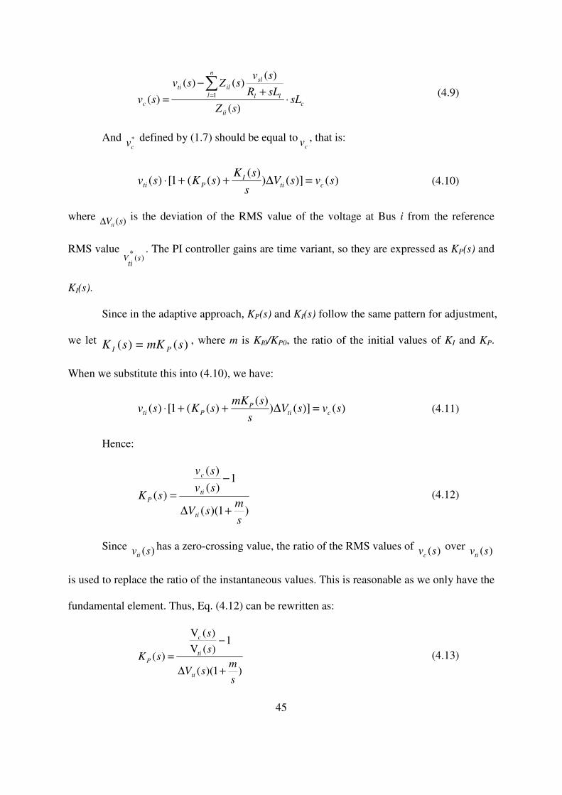
45
c
ii
n
l ll
sl
ilti
c sLsZ
sLR
svsZsv
sv ⋅+
−
=∑
=
)(
)()()(
)(1 (4.9)
And *
cv defined by (1.7) should be equal to
cv , that is:
)()]())(
)((1[)( svsVs
sKsKsv cti
IPti =∆++⋅ (4.10)
where )(sVti∆ is the deviation of the RMS value of the voltage at Bus i from the reference
RMS value )(
*s
tiV
. The PI controller gains are time variant, so they are expressed as KP(s) and
KI(s).
Since in the adaptive approach, KP(s) and KI(s) follow the same pattern for adjustment,
we let )()( smKsK PI = , where m is KI0/KP0, the ratio of the initial values of KI and KP.
When we substitute this into (4.10), we have:
)()]())(
)((1[)( svsVs
smKsKsv cti
PPti =∆++⋅ (4.11)
Hence:
)1)((
1)(
)(
)(
s
msV
sv
sv
sK
ti
ti
c
P
+∆
−
= (4.12)
Since )(svti
has a zero-crossing value, the ratio of the RMS values of )(svc
over )(svti
is used to replace the ratio of the instantaneous values. This is reasonable as we only have the
fundamental element. Thus, Eq. (4.12) can be rewritten as:
)1)((
1)(V
)(V
)(
s
msV
s
s
sK
ti
ti
c
P
+∆
−
= (4.13)

46
Based on the assumption that the ideal voltage response is an exponential response,
we have:
τ/1)( max
+
∆=∆
s
VsVti (4.14)
where maxV∆ is the magnitude of the voltage step change and τ is the time constant, which
can be defined according to the users’ requirement for response speed.
Hence, the voltage at Bus i can be derived as:
)2cos()()( max
* φπτ +∆−=−
fteVtv
t
ti tiV (4.15)
and
)/1
()( max*
τ+
∆−=
s
VsV
tiVti (4.16)
where φ is the phase angle of the voltage at terminal Bus i, and f is the fundamental
frequency.
By substituting Eqs. (4.9), (4.14), and (4.16) into (4.13), we can finally calculate KP(s)
and hence, KI(s). They are given as:
)1(/1
1
)/1
(
))(
RMS(
)(max
max*
s
m
s
Vs
V
sLSZ
A
sKti
V
c
ii
P
+⋅+
∆
−
+
∆−
⋅
=
τ
τ
(4.17)
)1(/1
1
)/1
(
))(
RMS(
)(max
max*
s
m
s
Vs
V
sLSZ
A
msKti
V
c
ii
I
+⋅+
∆
−
+
∆−
⋅
=
τ
τ
(4.18)

47
where:
∑
∑
=
−
=
+−+∆−=
+−=
n
l ll
sl
il
t
n
l ll
sl
ilti
sLR
svsZfteV
sLR
svsZsvA
tiV
1
max
1
)()()2cos()(
)()()(
* φπτ
(4.19)
Thus, we have proven that theoretical formulations for both KP(s) and KI(s) exist for
the ideal, exponential response of the voltage regulation. These formulations will be used to
confirm that the heuristic approach for adaptive control is equivalent to using KP(s) and KI(s)
in Eqs. (4.17) and (4.18).
However, in most application cases, we do not have enough data to calculate KP(s)
and KI(s). Even if we do, it is tedious and error-prone work to perform since multiple
distribution system parameters are involved. However, given the reference voltage and the
desired response speed, KP and KI can be automatically adjusted, as shown in the adaptive
algorithm in Section 4.2, to track the defined ideal response.
Figure 4.6 shows a comparison of the value of KP calculated by the theoretical
equation (4.17) and by the adaptive algorithm in Section 4.2. The simulation is performed on
the system as shown in Figure 4.5 with the DE modeled as an ideally controlled voltage
source. A load increase is applied at 0.2s to mimic voltage sag. The desired compensator
response time is 0.5s so it must reach the original voltage schedule at 0.7s. The solid blue line
Figure 4.5. A radial test system.

48
is KP calculated theoretically using (4.17) and the dashed red curve is KP generated by the
adaptive control approach. As can be seen, these two curves are extremely close, thus
verifying the heuristic approach with the theoretical formulations. Similarly, Figure 4.7
shows the comparison of KI for the two methods, which again shows an extremely close
match. In addition, Figure 4.8 shows the voltage regulation results by adjusting KP and KI
with the two methods. The dashed red line is the defined ideal response. The solid blue line is
the voltage response of the adaptive control approach and the dash-dot black line is the
voltage response with KP and KI calculated using Eqs. (4.17-4.18). The dotted red (flat) line is
the reference voltage.
The results in Figures 4.6-4.8 verify the equivalence of Equations (4.17-4.18) with the
adaptive algorithm of Section4.2, thus verifying the heuristic approach with a theoretical
foundation. The ideal response, defined as an exponential response, can be achieved by
dynamically adjusting KP and KI.
0.3 0.4 0.5 0.6 0.7 0.8 0.9 1 1.1 1.20.005
0.01
0.015
0.02
0.025
0.03
0.035
0.04
0.045
time(s)
Kp
Kp generated by adaptive method
Kp caculated theoreticallyusing(4.17)
Figure 4.6. Comparison of the value of KP generated by the two methods.

49
0.3 0.4 0.5 0.6 0.7 0.8 0.9 1 1.1 1.2
0.05
0.1
0.15
0.2
0.25
0.3
time(s)
Ki
Ki generated by adaptive method
Ki caculated theoreticallyusing (4.18)
Figure 4.7. Comparison of the value of KI generated by the two methods.
0.2 0.3 0.4 0.5 0.6 0.7 0.8 0.9 1 1.1 1.2267
268
269
270
271
272
time(s)
Voltage(v
)
Voltage reference
Voltage responsewith adaptive method
Desired voltage response
Voltage response with KpKicaculated theoreticallyusing(4.17-4.18)
Figure 4.8. Tracking ideal response by adjusting KP and KI with the two methods.

50
4.4. Simulation Results
In this section, a step-by-step example is shown to illustrate how to implement the
heuristic adaptive algorithm for voltage regulation as discussed in Section 4.2. The system in
Figure 4.5 is used again for illustration.
4.4.1. Initial Parameter Setting
As before, the DE is connected at Bus 3. The line-to-line voltage on the consumer
side of the infinite bus is assumed to be 480 V (RMS). The total load of the system is
70.18kVA (59 kW, 38kVar). We assume that the heaviest load condition is when the loads at
Bus 4 and Bus 6 increase by 20.93kVA (20.3 kW, 5.08 kVar) and 27.94kVA (27.1 kW, 6.8
kVar), respectively. The desired phase voltage profile at Bus 3 is 271.65 V (line-to-neutral,
RMS); however, the phase voltage at Bus 3 for the peak load condition is 267.2 V. From this
information, we can determine the DE requirements for voltage regulation.
1) Calculate the DC voltage requirement of the DE (Vdc).
Here the DE and substation bus can be viewed as the voltage resources. Hence, the
voltage at the load buses, such as Bus 3, can be expressed as follows:
cDEsubsub VaVaV ,3,33 += (4.20)
where 3Vis the voltage at Bus 3;
subV is the voltage at the substation bus, which can be
viewed as a constant; cVis the output voltage of the DE; and the coupling coefficients
suba ,3
and DEa ,3
represent the sensitivity between the two bus voltages (i.e.,
subV
V
∂
∂ 3
and
cV
V
∂
∂ 3
,
respectively), which can be calculated with network parameters.
In this case, we have:
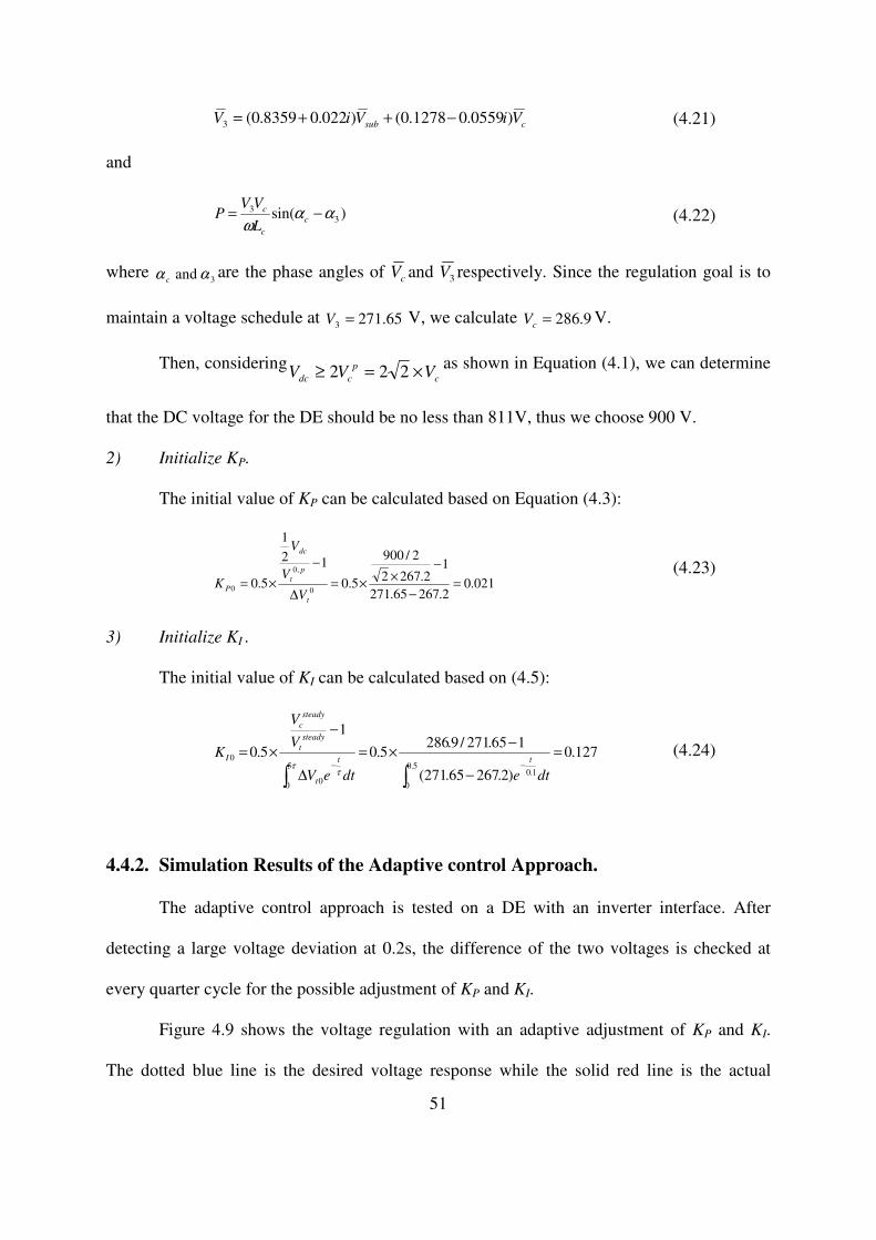
51
csub ViViV )0559.01278.0()022.08359.0(3 −++= (4.21)
and
)sin( 3
3 ααω
−= c
c
c
L
VVP (4.22)
where 3and αα care the phase angles of cV and 3V respectively. Since the regulation goal is to
maintain a voltage schedule at 65.2713 =V V, we calculate 9.286=cV V.
Then, consideringc
p
cdc VVV ×=≥ 222as shown in Equation (4.1), we can determine
that the DC voltage for the DE should be no less than 811V, thus we choose 900 V.
2) Initialize KP.
The initial value of KP can be calculated based on Equation (4.3):
021.02.26765.271
12.2672
2/900
5.0
12
1
5.00
,0
0 =−
−×
×=∆
−
×=t
p
t
dc
PV
V
V
K (4.23)
3) Initialize KI .
The initial value of KI can be calculated based on (4.5):
127.0
)2.26765.271(
165.271/9.2865.0
1
5.05.0
0
1.05
00
0 =
−
−×=
∆
−
×=
∫∫−−
dtedteV
V
V
Ktt
t
steady
t
steady
c
Iτ
τ
(4.24)
4.4.2. Simulation Results of the Adaptive control Approach.
The adaptive control approach is tested on a DE with an inverter interface. After
detecting a large voltage deviation at 0.2s, the difference of the two voltages is checked at
every quarter cycle for the possible adjustment of KP and KI.
Figure 4.9 shows the voltage regulation with an adaptive adjustment of KP and KI.
The dotted blue line is the desired voltage response while the solid red line is the actual

52
voltage response. As indicated, the actual voltage tracks the desired voltage response and
satisfies the 0.5s response time requirement. Figure 4.10 shows the comparison of the desired
and actual voltage deviations. The actual voltage response matches the reference voltage
except at the very beginning of the adjustment. The reason for the relatively large difference
at the very beginning is due to the initial high sensitivity of the voltage and the dominance of
the proportional part in Eq. (1.7) over the integral part. Hence, any small inaccuracy tends to
lead to a relatively large difference. However, when time approaches 0.3s, the proportional
part has less weight and the integral part has more effect. Therefore, the actual voltage
response curve is controlled very close to the desired curve.
In addition, Figures 4.11 and 4.12 are the real and reactive power injections,
respectively, during the voltage regulation. It should be noted that the P injection in Figure
4.11 remains constant except for small ripples around 0.2-0.4 s. These occur simply because
of the terminal voltage dynamics.
For verification purposes, Figure 4.13 shows the non-adaptive voltage regulation with
gains fixed to their initial values of KP0 and KI0. The response is much slower when compared
to the adaptive control approach. Instead of 0.5s, it takes more than 1s to reach the voltage
reference. Thus, the proposed adaptive control approach provides greater response efficiency.

53
0.2 0.3 0.4 0.5 0.6 0.7 0.8 0.9 1 1.1 1.2267
268
269
270
271
272
273
(s)
Voltage(v
)
Desired voltage response
Voltage reference
Actual voltage response
Figure 4.9. Voltage regulation with adaptive adjustment of KP and KI.
0.2 0.3 0.4 0.5 0.6 0.7 0.8 0.9 1 1.1 1.2
0
0.5
1
1.5
2
2.5
3
3.5
4
4.5
time(s)
Voltage e
rror(v)
Actual voltage error
Desired voltage error
Figure 4.10. Comparing the desired and actual voltage deviations.

54
0.2 0.4 0.6 0.8 1 1.210
20
30
40
time(s)
Real power injection(K
w)
Figure 4.11. Real power injection.
0.2 0.4 0.6 0.8 1 1.2
-5
0
10
20
30
time(s)
Reactive p
ower in
jection(K
var)
Figure 4.12. Reactive power injection.

55
0.2 0.4 0.6 0.8 1
267
268
269
270
271
272
273
time(s)
Voltage(v
)
Actual voltage response
Voltage reference
Desired voltage response
Figure 4.13. Non-adaptive voltage regulation with KP and KI fixed at the initial values.
4.5. Field Experiment Results at ORNL
The field experiment in this subsection is performed primarily by researchers at
ORNL including Dr. Yan Xu, Mr. D. Tom Rizy, and Mr. John D. Kueck. The results are
included here for the completeness of this dissertation, while credit should be attributed to
them.
Field tests were conducted at the Oak Ridge National Laboratory (ORNL)’s
Distributed Energy Communications & Controls (DECC) Laboratory, which is interfaced to
the ORNL distribution system and receives its power from the Tennessee Valley Authority
(TVA)’s bulk transmission system, as shown in Figure 4.14. The inverter of the DE test
system, which is rated at 150A, is connected to a 480V/600A power panel fed from circuit #2
of the 3000 substation of the ORNL distribution system.
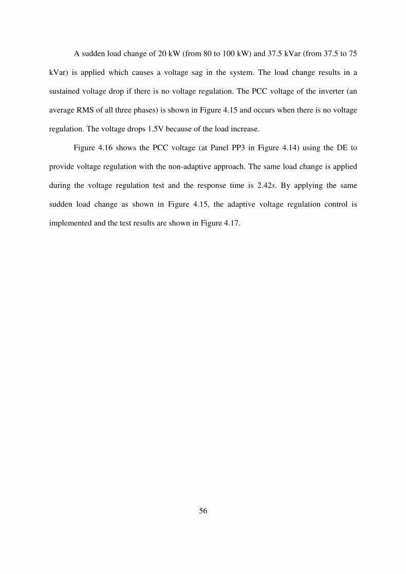
56
A sudden load change of 20 kW (from 80 to 100 kW) and 37.5 kVar (from 37.5 to 75
kVar) is applied which causes a voltage sag in the system. The load change results in a
sustained voltage drop if there is no voltage regulation. The PCC voltage of the inverter (an
average RMS of all three phases) is shown in Figure 4.15 and occurs when there is no voltage
regulation. The voltage drops 1.5V because of the load increase.
Figure 4.16 shows the PCC voltage (at Panel PP3 in Figure 4.14) using the DE to
provide voltage regulation with the non-adaptive approach. The same load change is applied
during the voltage regulation test and the response time is 2.42s. By applying the same
sudden load change as shown in Figure 4.15, the adaptive voltage regulation control is
implemented and the test results are shown in Figure 4.17.

57
Figure 4.14. ORNL’s DECC Laboratory.

58
Figure 4.15. PCC voltage at the inverter without voltage regulation.
Figure 4.16. PCC voltage (in RMS) with non-adaptive voltage regulation.

59
The response time is significantly shortened to 0.44s without any overshoot or
oscillation, or instability problem. Figure 4.18 shows the actual voltage deviation from the
experiment (the blue line with ripples) and the desired voltage deviation under the ideal
exponential response (the smooth red line). The actual deviation decay time closely matches
the 5τ decay time of the ideal curve (0.5 s). The experimental result verifies the advantage of
the adaptive control approach.
Figure 4.17. PCC voltage (in RMS) with adaptive voltage regulation.

60
Figure 4.18. Comparison of the desired and actual voltage deviations.
4.6. Chapter Conclusion
An adaptive voltage control approach using PI feedback control, which is based on
the local voltage variation and non-active power theory [10], is developed. The approach has
a wide adaptability and is easy to implement by practicing engineers since it does not require
detailed system data. Simulations and field experiments both show that the adaptive approach
satisfies the rapid response and performance requirements needed for integration with
existing system equipment.

61
5. Voltage Regulation with Multiple DEs
5.1. Chapter Introduction
In this chapter, the challenges of voltage regulation with multiple DEs are discussed.
A theoretical calculation of the controller parameters of the adaptive method in multiple DEs
voltage regulation is presented. Based on the availability of the communications among the
voltage regulating DEs, a high-end with communication implementation and low-end without
communication implementation of the adaptive control method are proposed, respectively.
Simulation results show that in both implementations, DEs can track the desired response
curve closely and yield satisfactory regulation results.
5.2. Challenges in Voltage Control with Multiple DEs
When multiple DEs connected in the systems participate in the voltage regulation, the
interference among these DEs makes the voltage control process more complicated. As
shown in the simulations in Chapter 3, the controller parameters suited for voltage regulation
with a single DE may fail to generate satisfactory performance in voltage regulation in the
two DEs case. The problem of coordination among all the DE controllers needs to be
considered as the DEs have similar response time that may cause them to chase each other
which could lead to instability or oscillations.
Note that in a practical operation, we may choose only a limited number of DEs for
voltage control, similar to the practice in AGC control. DEs with voltage regulation ability
can bid for providing this service such as in the ancillary service market. This should reduce
complexity while maintaining an acceptable efficiency. However, the exploration of how to
implement the process of choosing voltage regulating DEs in a large distribution system is

62
beyond the scope of this research and therefore will not be discussed in this dissertation.
Instead, it is assumed that the locations of the voltage regulating DEs are known.
In the following simulations, it is assumed that two DEs are installed at bus 3 (DE1)
and bus 6 (DE2), respectively, as shown in Figure 5.1. The five simulation scenarios can be
categorized into two types: only one DE offers the voltage regulation (Scenarios 1 and 4) or
both DEs participate in voltage regulation (Scenarios 2, 3, and 5). In all the scenarios, the
voltage reference at the PCC of DE2 remains fixed and the voltage reference setting of DE1
is varied in order to investigate the impact of the voltage regulation of DE1 on that of DE2.
The simulation conditions of each scenario are listed in Table 5.1.
Figure 5.2 shows the voltage responses of bus 6, where DE2 is connected, when the
voltage regulation settings of DE1 are varied. The controller parameters remain fixed with
KP=0.04 and KI=1.2 for both DEs in all the simulation scenarios. The red solid flat line is the
Table 5-1. Simulation conditions of the test scenarios.
Scenario
No.
If participating in voltage regulation Terminal voltage reference (v)
DE1 DE2 DE1 DE2
1 No Yes 270.2
2 Yes Yes 270.6 270.2
3 Yes Yes 271.0 270.2
4 Yes No 271.2
5 Yes Yes 271.2 270.2

63
voltage reference of DE2. The blue curve is the voltage response of DE2 in Scenario 1. The
magenta dash curve is the voltage response of DE2 in Scenario 2 and the green dot curve
shows the voltage response of DE2 in Scenarios 3. A comparison of voltage responses of
DE2 in the three scenarios shows that the voltage regulation behavior of DE1 affects the
terminal voltage response of DE2.
Figures 5.3 and 5.4 show the voltage responses of DE1 in Scenarios 2 and 3,
respectively. As seen in Figures 5.2 to 5.4, when the voltage reference of DE1 is set to 271v,
both DEs try to bring the voltage up and inject reactive power, which make the regulation
process of DE2 faster than the case when there is only one DE to regulate the voltage; while
the voltage reference of DE1 is set to 270.6 v in Figure 5.3, DE1 reduces the voltage, which
is the opposite direction to the voltage change of DE2. This slows down the regulation
process.
Figure 5.1. A radial test system installed with two DEs.
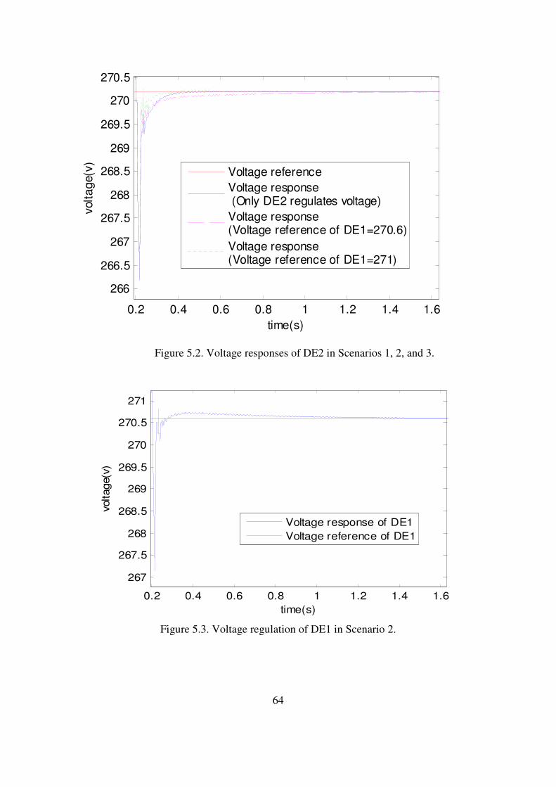
64
0.2 0.4 0.6 0.8 1 1.2 1.4 1.6
266
266.5
267
267.5
268
268.5
269
269.5
270
270.5
time(s)
volt
age(v
)
Voltage reference
Voltage response (Only DE2 regulates voltage)
Voltage response(Voltage reference of DE1=270.6)
Voltage response(Voltage reference of DE1=271)
Figure 5.2. Voltage responses of DE2 in Scenarios 1, 2, and 3.
0.2 0.4 0.6 0.8 1 1.2 1.4 1.6
267
267.5
268
268.5
269
269.5
270
270.5
271
time(s)
voltage(v
)
Voltage response of DE1
Voltage reference of DE1
Figure 5.3. Voltage regulation of DE1 in Scenario 2.

65
0.2 0.4 0.6 0.8 1 1.2 1.4 1.6267
267.5
268
268.5
269
269.5
270
270.5
271
time(s)
voltage(v
)
voltage reference of DE1
voltage response of DE1
Figure 5.4. Voltage regulation of DE1 in Scenario 3.
Besides changing the response speed of the other DEs, the voltage regulation
behavior of one DE may cause the wrong regulation direction problem of the other DEs. This
is demonstrated in the following discussion.
Recall that
]
0
))()(*())()(*
(1)[(*
dt
t
tt
Vtt
VI
Ktt
Vtt
Vp
Ktt
vc
v ∫ −+−+= . (5.1)
This is the reference voltage required for a DE to produce during the regulation
process. For fixed control parameters KP and KI with a positive value (usually KI is greater
than KP), if the reference voltage Vt*(t) is higher than the terminal voltage Vt(t), the DE will
increase its output voltage and attempt to bring the voltage up to the reference. On the other
hand, if Vt*(t) is less than Vt(t), the DE will reduce its output voltage and reduce the actual
voltage. When only a single DE regulates the voltage, the positive or negative sign of the
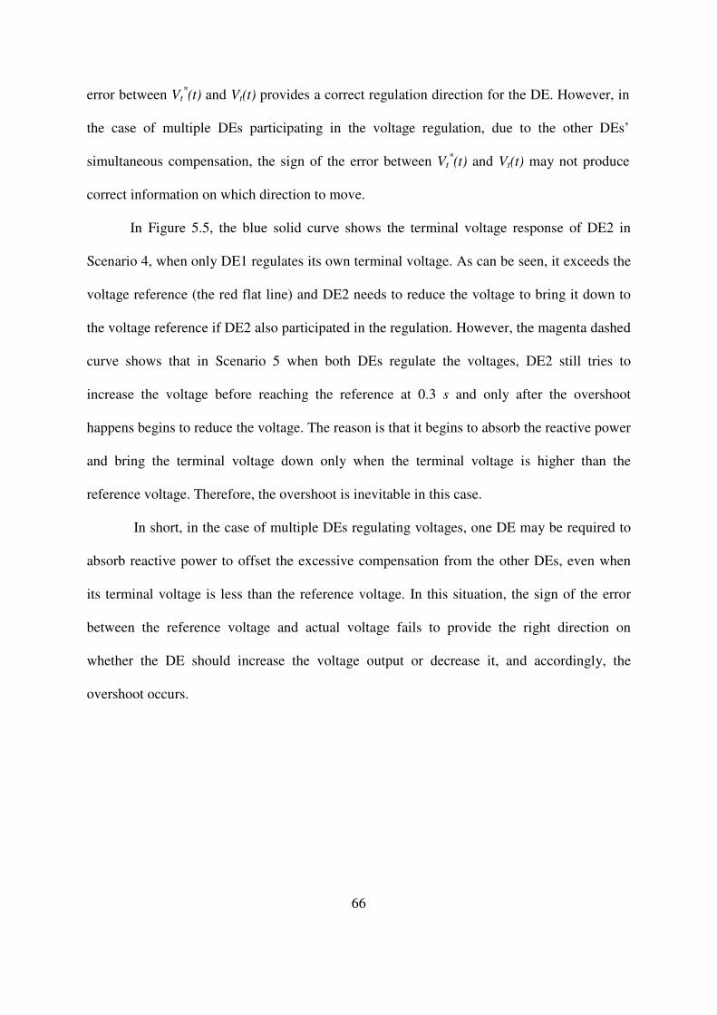
66
error between Vt*(t) and Vt(t) provides a correct regulation direction for the DE. However, in
the case of multiple DEs participating in the voltage regulation, due to the other DEs’
simultaneous compensation, the sign of the error between Vt*(t) and Vt(t) may not produce
correct information on which direction to move.
In Figure 5.5, the blue solid curve shows the terminal voltage response of DE2 in
Scenario 4, when only DE1 regulates its own terminal voltage. As can be seen, it exceeds the
voltage reference (the red flat line) and DE2 needs to reduce the voltage to bring it down to
the voltage reference if DE2 also participated in the regulation. However, the magenta dashed
curve shows that in Scenario 5 when both DEs regulate the voltages, DE2 still tries to
increase the voltage before reaching the reference at 0.3 s and only after the overshoot
happens begins to reduce the voltage. The reason is that it begins to absorb the reactive power
and bring the terminal voltage down only when the terminal voltage is higher than the
reference voltage. Therefore, the overshoot is inevitable in this case.
In short, in the case of multiple DEs regulating voltages, one DE may be required to
absorb reactive power to offset the excessive compensation from the other DEs, even when
its terminal voltage is less than the reference voltage. In this situation, the sign of the error
between the reference voltage and actual voltage fails to provide the right direction on
whether the DE should increase the voltage output or decrease it, and accordingly, the
overshoot occurs.

67
0.2 0.4 0.6 0.8 1 1.2 1.4 1.6
266.5
267
267.5
268
268.5
269
269.5
270
270.5
time(s)
volt
ag
e(v
)
Voltage reference of DE2
Voltage response of DE2only DE1 regulate voltage
Voltage response of DE2both DEs regulate voltage
Figure 5.5. Voltage response of DE2 in scenario 4 and scenario 5.
From the simulation results of the five scenarios, we can conclude that:
o When multiple DEs participate in the voltage regulation, they interact with one
another. The terminal voltage response of each DE is the result of all the DE’s
regulation behavior, and therefore, its speed may be increased or decreased by the
other participating DEs.
o The voltage correction of the other DEs may result in excessive compensation at
one DE’s terminal bus, which makes the sign of the error between the reference
voltage and actual voltage fail to indicate whether the DE should increase output
voltage or decrease it without a voltage overshoot. To avoid this problem, a new
signal should be introduced to provide the correct regulation direction for the DE.

68
The interaction among the DEs raises additional challenges for voltage control. The
control algorithm needs to consider the impact from the other DEs and avoid the overshoot
problem caused by the misleading information from the voltage error signal. However, we
also can observe from the simulation results that the local terminal voltage measurement
reflects the impacts of the other DEs’ regulation on one specific DE. This information can
still be used as the feedback to adjust the controller parameters.
5.3. Theoretical Formulation of the Parameters for Multiple Voltage-
Regulating DEs with Adaptive Control Method
In Chapter 4, the formulation of the controller parameters in the case of a single
voltage-regulating DE with the adaptive algorithm has been explained. When multiple DEs
participate in the voltage regulation, as shown in Figure 5.6, it is interesting to investigate
whether the adaptive control algorithm can still be applied to each voltage-regulating DE and
the desired voltage response curve of each DE can be defined independently. This section
will answer these questions and present a theoretical formulation of the controller parameters
for multiple DEs with an adaptive algorithm.

69
1
m
n
Network
vcm
Lcm
Rsm
Lsm
vsm
Lc1
vc1
Rs1
Ls1
vs1
Rsn
Lsn
vsn
Figure 5.6. A schematic diagram of a network and with multiple DE sources.
Assume the DEs are connected at bus 1 through bus m, as shown in Figure 5.6. The
nodal voltage equation can be expressed as
+
+
++
++
=
++
++
nn
sn
mm
sm
mm
sm
cm
cm
s
c
c
tn
tm
tm
t
sLR
sv
sLR
sv
sLR
sv
sL
sv
sLR
sv
sL
sv
sv
sv
sv
sv
sY
)(
)(
)()(
)()(
)(
)(
)(
)(
)(
11
1
11
1
1
1
1
1
M
M
M
M
(5.2)
where Y(s) is the admittance matrix of the system; vti(s) is the voltage at bus i; vsl(s) is the
voltage source at bus l (l=1~n), excluding the DE source; Rl+Ll is the equivalent impedance
for the electrical connection from the voltage source vsl to the terminal buses l; vck(s) is the
output voltage of the DE source connected at bus k (k=1~m); and Lcl is the inductance for the

70
DE to the terminal bus k connection. From Equation (5.2), we can derive the voltages vector
as
+
+
++
++
=
++
++
nn
sn
mm
sm
mm
sm
cm
cm
s
c
c
tn
tm
tm
t
sLR
sv
sLR
sv
sLR
sv
sL
sv
sLR
sv
sL
sv
sZ
sv
sv
sv
sv
)(
)(
)()(
)()(
)(
)(
)(
)(
)(
11
1
11
1
1
1
1
1
M
M
M
M
(5.3)
where the impedance matrix Z(S) = [Y (S)] -1. From Equation (5.3), we can obtain the vector
of the regulated voltage as follows
⋅+
+
+
+
=
)(
)(
)(
)()(
)(
)(
)(
)(
)(
)(
)(
2
1
2
11
1
1
1
sv
sv
sv
sAsZ
sLR
sv
sLR
sv
sLR
sv
sZ
sv
sv
sv
cm
c
c
nn
sn
ii
si
s
tm
ti
t
M
M
M
M
M
M
(5.4)
where Z1(S) is the sub-matrix of Z(S) formed by rows 1 to m; Z2(S) is an additional sub-
matrix of Z(S) formed by rows 1 to m and columns 1 to m; and A(S) is the diagonal matrix
defined in Equation (5.5)
=
cm
c
sL
sL
sA
/10
0/1
)(
1
O (5.5)
From Equation (5.4), the vector of the DE output voltages can be expressed as

71
+
+
+
−
⋅=
−−
nn
sn
ii
si
s
tm
ti
t
cm
ci
c
sLR
sv
sLR
sv
sLR
sv
sZ
sv
sv
sv
sZsA
sv
sv
sv
)(
)(
)(
)(
)(
)(
)(
)()(
)(
)(
)(11
1
1
1
1
2
1
1
M
M
M
M
M
M
(5.6)
Based on the assumption of the adaptive control method, we have
τ/1)(
max_
+
∆=∆
s
VsV
ti
tiand (5.7)
)/1
()(max_
τ+
∆−= ∗
s
VsV
ti
ti tiV . (5.8)
Therefore, we have
)2cos()()( max_ i
t
titi fteVtvti
V φπτ +∆−=−∗ (5.9)
where Vti(s) is the RMS of the voltage at bus i; ∆Vti(s) is the error between Vti *, the reference
voltage at bus i, and Vti(s); Фi is the phase angle of the voltage at the terminal Bus i, and f is
the fundamental frequency. Фi is known as the pre-disturbance condition or what can be
obtained by the steady-state power flow calculation in the simulation.
By substituting Equation (5.9) into Equation (5.6), we can obtain
+
+
+
−
+∆−
+∆−
+∆−
⋅=
−
−
−
−−
nn
sn
ii
si
s
m
t
tm
i
t
ti
t
t
cm
ci
c
sLR
sv
sLR
sv
sLR
sv
sZ
fteV
fteV
fteV
sZsA
sv
sv
sv
tmV
tiV
tV
)(
)(
)(
)(
)2cos()(
)2cos()(
)2cos()(
)()(
)(
)(
)(11
1
1
max_
max_
1max_1
1
2
1
1
*
*
*
1
M
M
M
M
M
M
φπ
φπ
φπ
τ
τ
τ
(5.10)
For any bus i (i=1~m), where the DE is connected, we have

72
∑ ∑= =
−
+−+∆−⋅=
m
j
n
l ll
sl
jlj
t
tjtjijcicisLR
svZfteVVTsLsv
1 1
max_
)()2cos()()( φπτ
(5.11)
where Tij is the element at row i and column j in Z2(S)-1 and Zjl is the element of row j and
column l of Z(S).
From Section 4.3, recall that
)1)((
1)(V
)(V
)(
s
msV
s
s
sK
ti
ti
ci
Pi
+∆
−
= (5.12)
where m is KI0/KP0 , the calculation of which has been discussed in Section 4.2. For the DEs
having the same DC voltage ratings, it can be assumed that the values of m are the same for
simplicity.
By substituting Equation (5.7), (5.8) and (5.11) into (5.12), we have
)1(/1
1
)/1
(
))(
)2cos()((
)(max_
max_
1 1
max_
*
s
m
s
V
s
V
sLR
svZfteVVTsLRMS
sKti
ti
m
j
n
l ll
sl
jlj
t
tjtjijci
Pi
tiV
++
∆
−
+
∆−
+−+∆−
=
∑ ∑= =
−
τ
τ
φπτ
(5.13)
and
)1(/1
1
)/1
(
))(
)2cos()((
)(max_
max_
1 1
max_
*
s
m
s
V
s
V
sLR
svZfteVVTsLmRMS
sKti
ti
m
j
n
l ll
sl
jlj
t
tjtjijci
Ii
tiV
++
∆
−
+
∆−
+−+∆−
=
∑ ∑= =
−
τ
τ
φπτ
(5.14)
Equations (5.13) and (5.14) provide the formulations to calculate the parameters of
the adaptive voltage controller when multiple DEs participate in the voltage regulation. If

73
only one voltage-regulating DE exists in the system and we assume it is connected at bus i, Tij
should be equal to 1/Zii then Equations (5.13) and (5.14) are the same as Equations (4.17) and
(4.18).
We can calculate the controller parameters with which the terminal voltage follows
the exponential decay pattern, provided that the network parameters are known, using
Equations (5.13) and (5.14). In the situation that one of the DEs needs to absorb the reactive
power in advance when its voltage is still below the reference to prevent the voltage
overshoot, and it is highly interesting to investigate what the controller parameters would be.
To investigate this phenomenon, the controller parameters in Scenario 5, listed in Table 5.1,
are calculated by Equations (5.13) and (5.14). The results are shown in Figures 5.7 ~5.12.
Figures 5.7 and 5.8 depict the terminal voltage responses of DE1 and DE2,
respectively. From the two figures, we can observe that after a disturbance occurs at 0.2 sec
which causes the voltage drop, the voltage at both buses follows the exponential decay
pattern to reach the reference voltages. Different from the response of the fixed parameters
control, no overshoot occurs at the terminal bus of DE2. This means that the timely
regulation direction information can be achieved by following the defined ideal voltage
response (i.e., the exponential decay pattern), instead of comparing the actual voltage with
the fixed reference voltage. The KP and KI parameters of the controllers will change during
the regulation process to generate the exponential-decay-pattern response. Those parameters
are shown in Figures 5.9 ~ 5.12. It should be noted that both DEs are assumed to have the
same DC voltage rating, and therefore, have the same value of KI/KP, which is calculated in
Section 4.4. The KP and KI of the controller of DE1 are shown in Figures 5.9 and 5.10. They
vary with respect to time during the entire regulation process. Similar to what we observed in
the simulation results of the single DE case, both of the KP and KI parameters increase

74
gradually to reach a stable positive value. However, from the KP and KI values of the DE2
controller, shown in Figures 5.11 and 5.12, we can observe that the values of the parameters
KP and KI reduce to negative. It should be noted that the sign of the values of KP and KI
reflect the voltage regulation direction. To avoid voltage overshoot at the terminal bus of
DE2, the voltage output of DE2 needs to be reduced to absorb reactive power, even when the
actual voltage is lower than the reference voltage. Therefore, the KP and KI values have to be
negative to reduce the voltage output of the DE2.
0.2 0.4 0.6 0.8 1 1.2 1.4 1.6267.5
268
268.5
269
269.5
270
270.5
271
271.5
272
time(s)
voltage(v
)
voltage response
voltage reference
Figure 5.7. Terminal voltage of DE1 - Scenario 5.

75
0.2 0.4 0.6 0.8 1 1.2 1.4 1.6266
266.5
267
267.5
268
268.5
269
269.5
270
270.5
271
time(s)
voltage(v
)
voltage response
voltage reference
Figure 5.8. Terminal voltage of DE2 – Scenario 5.
0.2 0.4 0.6 0.8 1 1.2 1.4 1.60
0.01
0.02
0.03
0.04
0.05
0.06
time(s)
KP
1
Figure 5.9. The calculated value of KP of DE1 in adaptive control - Scenario 5.

76
0.2 0.4 0.6 0.8 1 1.2 1.4 1.60
0.05
0.1
0.15
0.2
0.25
0.3
0.35
time(s)
KI1
Figure 5.10. The calculated value of KI of DE1 in adaptive control - Scenario 5.
0.2 0.4 0.6 0.8 1 1.2 1.4 1.6-0.01
-0.009
-0.008
-0.007
-0.006
-0.005
-0.004
-0.003
-0.002
-0.001
0
time(s)
KP
2
Figure 5.11. The calculated value of KP of DE2 in adaptive control - Scenario 5.

77
0.2 0.4 0.6 0.8 1 1.2 1.4 1.6-0.06
-0.05
-0.04
-0.03
-0.02
-0.01
0
time(s)
KI2
Figure 5.12. The calculated value of KI of DE2 in adaptive control - Scenario 5.
The previous analysis and simulations prove that a unique solution for the control
parameters under any specific operation condition exists. They also prove the existence of a
unique solution of the dynamic, time-varying control parameters that will lead to the ideal
voltage response.
To control the voltage regulation behavior of multiple voltage-regulating DEs in the
grid, two possible solutions exist: control with communication or control without
communication.
1. A high-end, with communication solution: Communications among the DEs
enable each voltage-regulating DE to have the necessary information to make the
control decision. The terminal voltage of each DE which participates in the
voltage regulation is broadcast among the voltage regulation DE groups or is

78
reported to the control center. Then each DE voltage controller or the control
center has sufficient information to make the right control decision. This high-end
solution requires a continuous communication that may incur additional cost and
create reliability issues. It should be noted that this work assumes the
communication is ideal. Hence, the discussion of the actual communication is
ignored while the focus is on the investigation of the control method.
2. A low-end solution with no communication: Methods with or without light
communication are more preferable. In section 5.2, we have observed that the
voltage at one DE’s terminal bus also reflects the simultaneous impact from the
other DEs’ voltage regulation behavior. So, when compared with the desired
response pattern, the local voltage measurement can still provide accurate and
timely information of the regulation direction. With the suitable adjusting step size
and timely adjustment, it is still possible for each DE to track its desired voltage
response pattern closely and finally reach the reference voltage.
In the following subsections of this chapter, both the voltage regulation approaches, with
and without communication, will be investigated and the results will be compared. Features
of each approach are discussed.
5.4. Voltage Regulation with Communication
The communication among the voltage-regulating DEs or with the control center
provides the real time information of the whole system, including the terminal voltage at the
other DE buses and the output voltage of every DE.
At any time t, we have

79
+
+
++
++
=
•
++
+
•
••
••
•
+
•
•
•
snsn
sn
msms
sm
smsm
sm
cm
cm
ss
s
c
c
tnt
mt
tm
t
jXR
tV
jXR
tV
jXR
tV
jX
tV
jXR
tV
jX
tV
tV
tV
tV
tV
Y
)(
)(
)()(
)()(
)(
)(
)(
)(
)1()1(
1
11
1
1
1
1
)1(
1
M
M
M
M
(5.15)
where Y is the admittance matrix Yij=Gij+jBij and tititi VV δ∠=
•, (i=1~n).
Equation (5.15) is the discretization of function (5.2). For any bus, i, which is
connected with DE, from Equation (5.15) we can obtain
.~)1(,)()(
)()()(
.~1,)()()()(
)()()(
1
1
nmijXR
ttVttVjBG
mijXR
ttV
jX
ttVttVjBG
sisi
sisin
j
jtjjij
sisi
sisi
ci
cicin
j
jtjijij
+=+
∠=∠+
=+
∠+
∠=∠+
∑
∑
=
=
δδ
δδδ
(5.16)
By splitting Equation (5.16) into real part and imaginary parts, we have
.~1),(_))(sin()())(cos()(
.~1),(_))(sin()())(cos()(
.~1
),(_))(cos()(
))(cos()())(sin()(
.~1
),(_))(sin()(
))(sin()())(cos()(
1
1
1
1
nmitisourcettVBttVG
nmitrsourcettVBttVG
mi
tisourceX
ttVttVBttVG
mi
trsourceX
ttVttVBttVG
i
n
j
jtjijjtjij
i
n
j
jtjijjtjij
i
ci
cici
jtj
n
j
ijjtjij
i
ci
cicin
j
jtjijjtjij
+==−
+==−
=
+−
=+
=
+=−
∑
∑
∑
∑
=
=
=
=
δδ
δδ
δδδ
δδδ
(5.17)

80
where source_ri(t) and source_ii(t) are the real and imaginary parts of
sisi
sisi
jXR
ttV
+
∠ )()( δ ,
respectively. They are constants because the voltage sources from the substations are known,
as is typically assumed.
Considering the real power output of DEs, we have
.~1),())()(sin()()(
mitPttX
tVtViici
ci
tici ==− δδ (5.18)
In the adaptive control method, the terminal voltage response of each DE, Vi(t),
i=1~m, is predefined, so we have 2n+m unknown variables remaining. These 2n+m
unknowns include:
• The phase angles of the bus voltage )(tiδ ,i=1~n;
• The magnitudes of the voltage at the other buses, excluding DE terminal buses,
Vi(t), i=m+1~n;
• The phase angles of the DE output voltages, )(tciδ , i=1~m; and
• The magnitude of DEs output voltages, Vci(t) , i=1~m.
There are total of 2n+m equations in (5.17) and (5.18), which matches the total
number of the unknown variables. Hence, at any moment t, given the terminal voltage of DEs,
Vi(t), i=1~m, there are corresponding DE output voltages Vci(t), i=1~m.
.~1)),(),(()( 1 mitVtVftV mici == L (5.19)
From t0 to t0+∆t, if ∆Vi(t) is very small and Function (5.19) can be linearized to
acquire the approximation of Vci(t0+∆t) as
.~1)),()(()()( 00
1
00 0mitVttV
V
ftVttV jj
m
j
tt
j
i
cici =−∆+∂
∂+=∆+ ∑
=
= (5.20)

81
where
0tt
j
i
V
f=
∂
∂is assumed to be constant in the small range and can be calculated by the local
measurement in real time.
At t0, t0+∆t, t0+2∆t, …, t0+m∆t, without the loss of generality, we can set the output
voltages of DE at bus i are Vci (t0 ), Vci (t0+∆t ), Vci (t0+2∆t ), …, Vci (t0+m∆t ), respectively,
where i=1~m. The corresponding terminal voltages, Vj (t0 ), Vj (t0+∆t ), Vj (t0+2∆t ), …, Vj
(t0+m∆t ) , where j=1~m, at the buses which have DE connections can be measured. Hence,
for any bus i which has a DE connection, we have the following equations
∑
∑
∑
=
=
=
∆∂
∂=∆−+−∆+=∆
∆∂
∂=∆+−∆+=∆
∆∂
∂=−∆+=∆
m
j
m
j
j
i
cici
m
ci
m
j
j
j
i
cicici
m
j
j
j
i
cicici
VV
ftmtVtmtVV
VV
fttVttVV
VV
ftVttVV
1
)(
00
)(
1
)2(
00
)2(
1
)1(
00
)1(
))1(()(
)()2(
)()(
M
(5.21)
where mjmimktktVtktVV jj
k
j ~1,~1,~1 ),)1(()( 00
)( ===∆−+−∆+=∆.
Equation (5.21) can also be expressed in matrix form as
∂
∂
∂
∂∂
∂
∆∆∆
∆∆∆
∆∆∆
=
∆
∆
∆
m
i
i
i
m
m
mm
m
m
m
ci
ci
ci
V
f
V
f
V
f
VVV
VVV
VVV
V
V
V
ML
MMMM
L
L
M 2
1
)()(
2
)(
1
)2()2(
2
)2(
1
)1()1(
2
)1(
1
)(
)2(
)1(
(5.22)
We can derive the coefficient vector as

82
∆
∆
∆
∆∆∆
∆∆∆
∆∆∆
=
∂
∂
∂
∂∂
∂−
)(
)2(
)1(1
)()(
2
)(
1
)2()2(
2
)2(
1
)1()1(
2
)1(
1
2
1
m
ci
ci
ci
m
m
mm
m
m
m
i
i
i
V
V
V
VVV
VVV
VVV
V
f
V
f
V
f
M
L
MMMM
L
L
M
(5.23)
By Equation (5.23), we can obtain the linearized relation in a small range between all
DE output voltages and the voltages at all the DE terminals.
In the adjustment process, once the coefficient vectors have been calculated by (5.23),
we can easily calculate how much the DE output voltage needs to be for the next adjustment
step based on Equation (5.20) in order to achieve the voltage response matching the desired
response. When the voltage matches the desired response, it follows the pattern below
)(
)()(
)()(
max_
max_max_
00
)1(
**
ττ
ττ
ttt
j
t
tj
tt
tj
jjj
eeV
eVeV
tVttVV
tjV
tjV
∆+−−
−∆+
−
−∆=
∆−−∆−=
−∆+=∆
(5.24)
from t0 to t0+∆t; and
)()()2(
2
max_00
)2( ττ
tttt
tjjjj eeVttVttVV
∆+−
∆+−
−∆=∆+−∆+=∆ (5.25)
from t0+∆t to t0+2∆t.
For two consecutive voltage changes, we can obtain the ratio of the two by dividing
(5.25) by (5.24),
mj
e
ee
eeV
eeV
V
Vr
t
tt
ttt
tj
tttt
tj
j
j~1,
1)(
)(2
max_
2
max_
)1(
)2(
=
−
−=
−∆
−∆=
∆
∆=
∆−
∆−
∆−
∆+−−
∆+−
∆+−
τ
ττ
ττ
ττ
. (5.26)

83
Provided that the fixed step size, ∆t, of the parameter-adjusting process, the ratio is
constant and remains the same for each DE terminal voltage. Therefore, from Equation (5.20),
we have
)1()1(
1
)1(
1
)2(
1
00
)2(
0
00
)()2(
cij
m
j
tt
j
j
m
j
tt
j
j
m
j
ttt
j
cicici
VrVV
fr
VrV
fV
V
f
ttVttVV
∆=∆∂
∂=
∆∂
∂≈∆
∂
∂=
∆+−∆+=∆
∑
∑∑
==
=
=
=
∆+=. (5.27)
We can conclude that the DE output voltage required to generate the desired response
should follow the following rule:
The ratio of two consecutive adjustments is constant and equal to the ratio of
the corresponding two consecutive terminal voltage changes.
So, after the terminal voltage response matches the desired response, the DE output
voltage can be adjusted according to this rule to make the voltage response follow the desired
response. In the following adjusting process, the coefficient vector T
m
iii
V
f
V
f
V
f
∂
∂
∂
∂
∂
∂,,,
21
L
does not need to be calculated, and actually, Equation (5.23) does not exist when the voltage
follows the desired exponential decay paten because
∆∆∆
∆∆∆
∆∆∆
)()(
2
)(
1
)2()2(
2
)2(
1
)1()1(
2
)1(
1
m
m
mm
m
m
VVV
VVV
VVV
L
MMMM
L
L will
become singular in this condition.
The regulating algorithm discussed so far can be generalized into three steps:
1. Increasing the DEs voltage output by a fixed step to calculate the coefficient
vector T
m
iii
V
f
V
f
V
f
∂
∂
∂
∂
∂
∂,,,
21
L
.

84
2. Setting the DE voltage outputs according to Equation (5.20) to ensure each DE
terminal voltage to match the desired response.
3. Updating the DEs voltage output according to Equation (5.27).
A more detailed algorithm flow chart is shown in Figure 5.13.
In the following discussion, the simulation results of the adaptive voltage control
method with communication on the system in Figure 5.1 will be shown. The real power
injection of DE1 and DE2 is 30 kW and 10 kW, respectively, and remains constant. The
voltage references for bus 3 and bus 6 are 275.85 v and 275.70 v. Assume after a load
increase, the voltages at bus 3 and bus 6 drop to 270.85 v and 270.70 v, respectively. The
adjustment cycle is 1/60 s (i.e., the adjustment frequency is aligned with the electricity
frequency).
1. Calculating the coefficient vector T
m
iii
V
f
V
f
V
f
∂
∂
∂
∂
∂
∂,,,
21
L
.
V(0)=[270.85, 270.5]T, Vc(0)=[271.1726, 270.1228]T. Increase DE output voltage by
∆Vc(1)=[0.1,0.1]T and ∆Vc
(2)=[0.1,0.15]T in two consecutive adjustment processes.
Then, we have Vc(1)=[271.2726, 270.2228]T and Vc
(2)=[271.3726, 270.3728]T. The
corresponding terminal voltages are V(1)=[270.8758, 270.5267]T and V(2)=[270.9074,
270.5598]T . According to Equation (5.23), for DE1 we have
=
−−
−−=
∆
∆
∆∆
∆∆=
∂
∂∂
∂
−
−
60.7167-
66.7170
1.0
1.0
5267.2705598.2708758.2709074.270
5.2705267.27085.2708758.2701
)2(
1
)1(
1
1
)2(
6
)2(
3
)1(
6
)1(
3
6
1
3
1
c
c
V
V
VV
VV
V
f
V
f

85
If | Vref-Vactual|>threshhold
Detect the maximum voltage deviation
and record current Vc and Vt
If the number of the measurements equals the
number of the voltage-regulating DEs
Increase Vc by fixed step
and record corresponding Vt
Calculate the coefficient
vectors
Set Vc according to Eq.
(5.20),and record
corresponding Vt
Calculate △Vc, △Vt and
ratio r
Update Vc according o
Eq.(5.27)
Yes
If | Vref-Vactual|>threshhold
No
EndNoYes
No
Initialize the ratio between
controller parameters according
to Eqs. (4.3) and (4.5)
Figure 5.13. Adaptive voltage adjusting algorithm with communication.

86
For DE2, we have
=
−−
−−=
∆
∆
∆∆
∆∆=
∂
∂∂
∂
−
−
72.2351
70.8723-
15.0
1.0
5267.2705598.2708758.2709074.270
5.2705267.27085.2708758.2701
2
2
)1(
2
1
)2(
6
)2(
3
)1(
6
)1(
3
6
2
3
2
c
c
V
V
VV
VV
V
f
V
f
2. Adjusting DE output voltages to make terminal voltage match the desired
response.
The desired voltage at bus 3 is 8173.272585.275 1.0
60/13
=−×
−
e V, and at bus 6 is
5460.2722.57.275 1.0
60/13
=−×
−
e V. According to Equation (5.20), the voltage
adjustments need to be
=
−
−
−
−=
∆
∆
∂
∂
∂
∂∂
∂
∂
∂
=
∆
∆
8.1155
6.8265
5598.2705460.272
9074.2708173.272
2351.728723.70
7167.607170.66
)3(
_6
)3(
_3
6
2
3
2
6
1
3
1
)3(
2
)3(
1
desired
desired
c
c
V
V
V
f
V
f
V
f
V
f
V
V
After the adjustments, the output voltages of two DEs are
=
+
+=
278.4883
278.1991
8.1155270.3728
6.8265271.3726)3(
2
)3(
1
c
c
V
V.
The corresponding terminal voltages are V(3)=[272.8061, 272.5350]T, which are very
close to the desired response.
For the next adjusting process, we have the desired response as

87
=
−
−= ×−
×−
0302.273
2829.273
2.57.275
585.275
1.0
60/14
1.0
60/14
)4(
e
eVdesired
To match the desired response, the DEs output voltages need to be
=
−
−
−
−+
=
∆
∆
∂
∂
∂
∂∂
∂
∂
∂
+
=
280.4736
279.9373
5350.2720302.273
8061.2722829.273
2351.728723.70
7167.607170.66
278.4883
278.1991
)4(
_6
)4(
_3
6
2
3
2
6
1
3
1
)3(
2
)3(
1
)4(
2
)4(
1
desired
desired
c
c
c
c
V
V
V
f
V
f
V
f
V
f
V
V
V
V
The actual voltages are Vt(4)=[273.2768, 273.0242]T. The voltage responses at both
buses follow the desired response.
Similar patterns will be repeated for the following processes.
3. Adjusting DE output based on the ratio of voltage change between two
consecutive adjusting steps.
If the voltage responses perfectly follow the desired responses without any error, the
ratio of the two consecutive voltage changes can be calculated by applying equation
(5.26) as
8465.0
11 1.0
60/1
1.0
60/2
1.0
60/12
=
−
−=
−
−=
−
−−
∆−
∆−
∆−
e
ee
e
eer
t
tt
τ
ττ
.
The actual needed ratio can be calculated as:1−∆
∆=
i
i
desired
V
Vr . For multiple DEs, we can
take the average value of all the DEs to neutralize the random errors. In this case, we
have
8502.02/5350.2720242.273
0242.2734401.273
8061.2722768.273
2768.2736770.273=
−
−+
−
−=r .

88
And hence, the DE output for this step should be
=
+
=
∆
∆+
=
282.1614
281.4152
9853.1
7383.18502.0
280.4736
279.9373)4(
2
)4(
1
)4(
2
)4(
1
)5(
2
)5(
1
c
c
c
c
c
c
V
Vr
V
V
V
V.
The corresponding terminal voltages are Vt(5)=[273.6760, 273.4392]T. The actual
voltages closely follow the desired responses. For the following adjusting steps, this
operation will be repeated until the actual responses reach the voltage references.
Figures 5.14 and 5.15 show the comparison of the actual voltage responses and
desired voltage responses in the whole process. The voltage drop occurs at 0.2 sec. At the
beginning of the regulation process, the voltage response does not follow the ideal response
because the DEs’ output voltages are controlled to increase in the fixed step size to calculate
the coefficients between the DEs’ output voltage changes and the terminal voltage changes.
After obtaining the coefficients, the voltage responses successfully catch the ideal responses
and going forward follow the ideal responses very closely until reaching the reference
voltages. The maximum difference of the ideal voltage and actual voltage is 0.0112 V for
DE1 and 0.0111 V for DE2 in the process. Figures 5.16~5.19 show the values of the KP and
KI parameters of the DE1 and DE2 controllers, respectively, in the adjustment process. Figure
5.20 shows the average value of the ratio of the two consecutive voltage changes, which is
close to the ideal value 0.8465.
This method is also tested in the case that one DE needs to absorb reactive power.
Figures 5.21 and 5.22 show the voltage responses at terminals DE1 and DE2, respectively,
when only DE1 regulates its terminal voltage. The terminal voltage of DE2 finally reaches
275.48 V. If the reference voltage at the terminal of DE2 is set to 271.10 V, DE2 needs to
absorb reactive power. Figures 5.23~5.29 show the simulation results when both DEs

89
regulate the voltage, when the reference voltages of DE1 and DE2 are 275.85 V and 275.10
V, respectively. The terminal voltage responses of DE1 and DE2 can closely track the ideal
responses except at the very beginning, as shown in Figures 5.23 and 5.24. After obtaining
the coefficient vector, the maximum tracking errors are 0.0576 V and 0.0566 V, respectively.
The values of KP in the DE1 and DE2 controllers are shown in Figures 5.25 and 5.27,
respectively. The KP of DE2 decreases to a negative value to make the output voltage of DE2
less than the terminal voltage and therefore, DE2 absorbs the reactive power while its
terminal voltage is still below the reference. The average value of the ratio of the two
consecutive voltage changes during the regulation process, shown in Figure 5.29, is close to
the ideal value 0.8465 as well. These simulation results show that this tracking method can
also work well in the case where the DE needs to absorb reactive power even when its
reference voltage is higher than its terminal voltage.
The control approach with the communication can directly calculate how much the
DEs output voltages need to be in order to match the desired response curve and hence can
track the desired response quite closely.

90
0.2 0.4 0.6 0.8 1.0 1.2 1.4 1.6
271
271.5
272
272.5
273
273.5
274
274.5
275
275.5
276
time(s)
voltage(v
)
desired voltage response
actual voltage response
voltage reference
Figure 5.14 Voltage response of DE1 using the with-communication method when the
reference voltages of DE1 and DE2 are 275.85 V and 275.70 V, respectively.
0.2 0.4 0.6 0.8 1.0 1.2 1.4 1.6270.5
271
271.5
272
272.5
273
273.5
274
274.5
275
275.5
276
time(s)
voltage(v
)
desired voltage response
actual voltage response
voltage reference
Figure 5.15. Voltage response of DE2 using the with-communication method when the
reference voltages of DE1 and DE2 are 275.85 V and 275.70 V, respectively.

91
0.2 0.4 0.6 0.8 1.0 1.2 1.4 1.60
0.002
0.004
0.006
0.008
0.01
0.012
0.014
0.016
time(s)
Kp1
Figure 5.16. KP of DE1 using the with-communication method when the reference voltages of
DE1 and DE2 are 275.85 V and 275.70 V, respectively.
0.2 0.4 0.6 0.8 1.0 1.2 1.4 1.60
0.01
0.02
0.03
0.04
0.05
0.06
0.07
0.08
0.09
0.1
time(s)
KI1
Figure 5.17. KI of DE1 using the with-communication method when the reference voltages of
DE1 and DE2 are 275.85 V and 275.70 V, respectively.
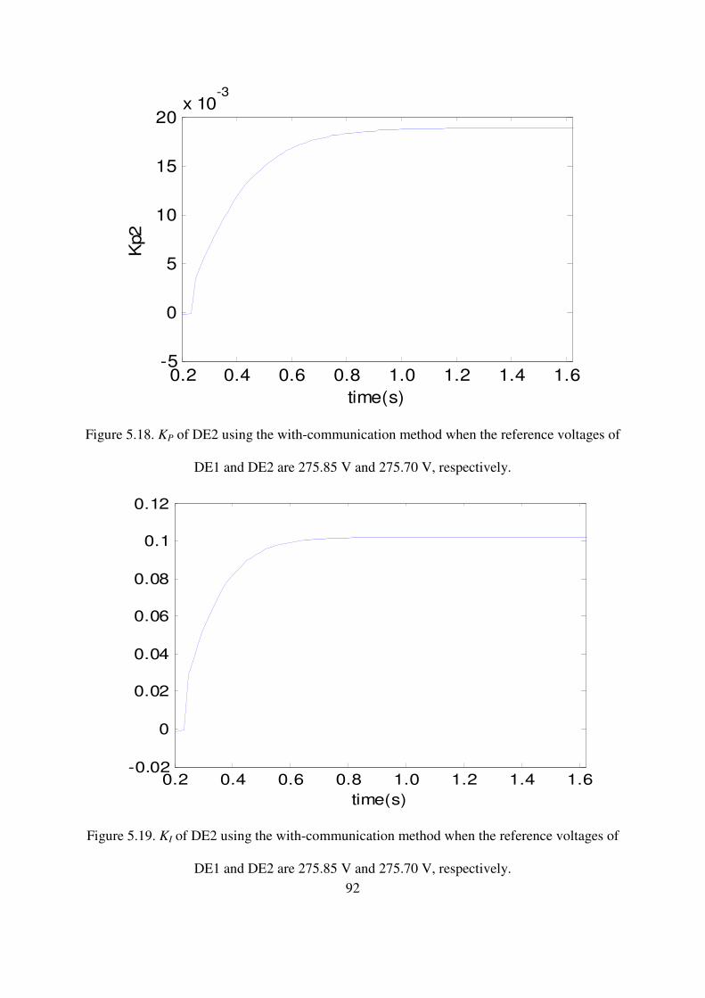
92
0.2 0.4 0.6 0.8 1.0 1.2 1.4 1.6-5
0
5
10
15
20x 10
-3
time(s)
Kp2
Figure 5.18. KP of DE2 using the with-communication method when the reference voltages of
DE1 and DE2 are 275.85 V and 275.70 V, respectively.
0.2 0.4 0.6 0.8 1.0 1.2 1.4 1.6-0.02
0
0.02
0.04
0.06
0.08
0.1
0.12
time(s)
Figure 5.19. KI of DE2 using the with-communication method when the reference voltages of
DE1 and DE2 are 275.85 V and 275.70 V, respectively.

93
0.2 0.4 0.6 0.8 1.0 1.2 1.4 1.60.83
0.835
0.84
0.845
0.85
0.855
0.86
time(s)
ratio
Figure 5.20. Ratio of the two consecutive voltage changes using the with-communication
method when the reference voltages of DE1 and DE2 are 275.85 V and 275.70 V,
respectively.
0.2 0.4 0.6 0.8 1.0 1.2 1.4 1.6270
271
272
273
274
275
276
time(s)
voltage(v
)
voltage response of DE1
voltage reference
Figure 5.21. Voltage response of DE1 - only DE1 regulating voltage.
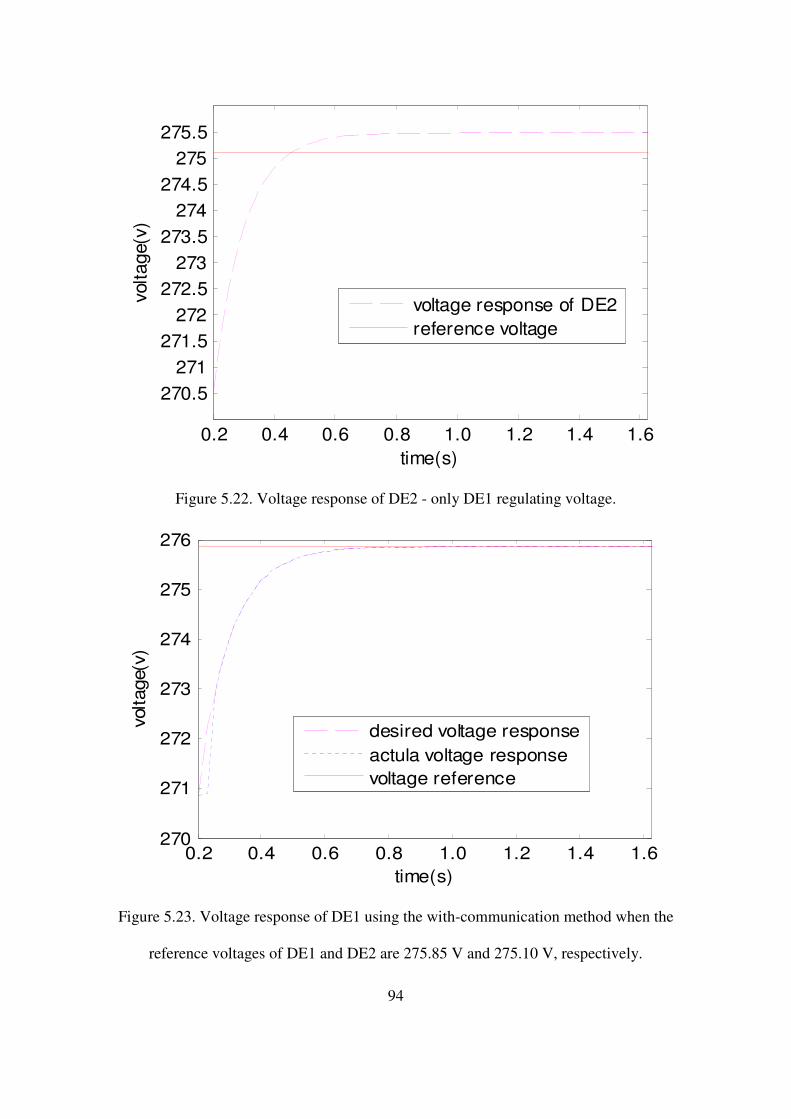
94
0.2 0.4 0.6 0.8 1.0 1.2 1.4 1.6
270.5
271
271.5
272
272.5
273
273.5
274
274.5
275
275.5
time(s)
voltage(v
)
voltage response of DE2
reference voltage
Figure 5.22. Voltage response of DE2 - only DE1 regulating voltage.
0.2 0.4 0.6 0.8 1.0 1.2 1.4 1.6270
271
272
273
274
275
276
time(s)
voltage(v
)
desired voltage response
actula voltage response
voltage reference
Figure 5.23. Voltage response of DE1 using the with-communication method when the
reference voltages of DE1 and DE2 are 275.85 V and 275.10 V, respectively.

95
0.2 0.4 0.6 0.8 1.0 1.2 1.4 1.6270
271
272
273
274
275
276
time(s)
voltage(v
)
desired voltage response
actual voltage response
voltage reference
Figure 5.24. Voltage response of DE2 using the with-communication method when the
reference voltages of DE1 and DE2 are 275.85 V and 275.10 V, respectively.
0.2 0.4 0.6 0.8 1.0 1.2 1.4 1.60
0.01
0.02
0.03
0.04
0.05
0.06
time(s)
kp
Figure 5.25. KP of DE1 using the with-communication method when the reference voltages of
DE1 and DE2 are 275.85 V and 275.10 V, respectively.

96
0.2 0.4 0.6 0.8 1.0 1.2 1.4 1.60
0.05
0.1
0.15
0.2
0.25
0.3
0.35
time(s)
KI1
Figure 5.26. KI of DE1 using the with-communication method when the reference voltages of
DE1 and DE2 are 275.85 V and 275.10 V, respectively.
0.2 0.4 0.6 0.8 1.0 1.2 1.4 1.6-0.035
-0.03
-0.025
-0.02
-0.015
-0.01
-0.005
0
time(s)
kp
Figure 5.27. KP of DE2 using the with-communication method when the reference voltages of
DE1 and DE2 are 275.85 V and 275.10 V, respectively.

97
0.2 0.4 0.6 0.8 1.0 1.2 1.4 1.6-0.2
-0.18
-0.16
-0.14
-0.12
-0.1
-0.08
-0.06
-0.04
-0.02
0
time(s)
KI2
Figure 5.28. KI of DE2 using the with-communication method when the reference voltages of
DE1 and DE2 are 275.85 V and 275.10 V, respectively.
0.2 0.4 0.6 0.8 1.0 1.2 1.4 1.60.8
0.81
0.82
0.83
0.84
0.85
0.86
0.87
0.88
time(s)
ratio
Figure 5.29. Ratio of the two consecutive voltage changes using the with-communication
method when the reference voltages of DE1 and DE2 are 275.85 V and 275.10 V,
respectively

98
5.5. Voltage Regulation without Communication
When communications among the DEs and/or with the control center are not available,
each DE can only use its local information to regulate voltage. However, it is already shown
by the simulation results in Subsection 5.1 that the terminal voltage of each DE also
implicitly reflects the other DEs’ voltage regulation behavior almost instantaneously.
Moreover, the ideal response curve instead of the reference voltage, which is fixed during the
regulation process, provides a timely signal of the adjusting direction. So it is possible to
adaptively modify DE’s output for voltage regulation to catch the ideal response and finally
reach the fixed reference by using only the local information with a higher frequency
adjustment.
The heuristic adaptive method is used in Chapter 4 to track the ideal response. In
chapter 4, a scaling factor is defined to adaptively modify the control parameters. In the
single-DE voltage-regulation case, the gain parameters are always positive since the DE
output voltage changes its direction (increase or decrease) in accordance with the direction
that the terminal voltage is required to change. However, in the case of multiple DEs, as
shown in the previous discussion in this Chapter, the gain parameters may be negative for
several DEs because the same direction rule in one DE case does not always hold true in this
case. Thus, the scaling factor will not work to generate the negative gains. An alternative
updating scheme which can generate either positive or negative gains is preferred. In the
updating scheme, two factors need to be considered: the direction and step size of the
adjustment.
A. Direction of the adjustment

99
The comparison of the actual voltage with the ideal voltage provides the information
for the adjusting direction. The change of DE output voltage caused by the adjustment of the
gain parameters can be expressed as
)())(()())()((1
)())(()())()((1
10
111
20
222
1
2
tVdttVVtKtVVtK
tVdttVVtKtVVtKV
t
refIrefP
t
refIrefPc
−+−+−
−+−+=∆
∫
∫
(5.28)
Since at every adjustment, the change of the terminal voltage is very small, V(t2) is
approximately equal to V(t1). Also, the difference between ∫ −
2
0))((
t
ref dttVVand
∫ −1
0))((
t
ref dttVVcan be neglected. Therefore, we have
)())(())(( 10
1
1
tVdttVVKtVVKVt
refIrefPc
−∆+−∆≈∆ ∫ (5.29)
When the actual local terminal voltage (V(t1)) is higher than the desired terminal voltage
(Vdesired), a DE needs to reduce its output voltage (Vc) to reduce the actual terminal voltage
and ∆Vc should be negative. Hence, according to Equation (5.29), to obtain a voltage
reduction, i.e., a negative ∆Vc, ∆KP needs to be positive if a voltage deviation beyond the
reference occurs (i.e. Vref < V(t)); or ∆KP needs to be negative if a voltage deviation below the
reference occurs (i.e. Vref > V(t)). To the contrary, when the actual local voltage is lower than
the desired voltage, the DE needs to increase its output voltage to bring the actual voltage up
and ∆Vc needs to be positive.
At any given time instant, it is not clear whether the DE should really bring the
voltage up or down because of the impact from other DEs, even though the DE’s local
voltage is lower (or higher) than the reference voltage. Therefore, based on these discussions,
the updating scheme of KP is proposed as a gradual change towards the desired direction. This

100
can help avoid the dramatic change of KP that may lead to an undesired voltage response. The
new updating scheme of KP is defined as
P
old
P
new
P KKK ∆+= (5.30)
=
−×−×=∆
d.becorrecte tois rise voltagewhen,1
; corrected be tois dip voltagewhen,0
));()(()1(
Sand
tVtVK actualideal
S
P α
(5.31)
where α is a positive value, which is the adaptive scaling factor and will be discussed next.
B. Step size of the adjustment
When the deviation of the actual voltage from the ideal voltage is large, a large
adjustment is expected; when the deviation is small, a small adjustment is desirable. Thus, it
is reasonable to define an adaptive scaling factor as
( )actualideal tVtVk )()(1 −+×=α (5.32)
where k is a fixed step size.
Since the ideal response is defined as an exponential decay curve, the largest step
change of the terminal voltage should occur at the first adjustment, as shown in Figure 5.30.
Additionally, in this adjustment, the corresponding DE output voltage change, ∆Vc, should
also be the largest. The relationship between ∆Vc and ∆V can be linearized as
∑=
∆=∆m
l
clli VcV1
(5.33)
where ilVcVc ciicll ≠∆<∆ , , and 1<lc , because the voltage change of the source produces
less impact on the voltage of the buses with longer electrical distance from the source. And
we can obtain
cicii
m
l
clli VmVmcVcV ∆<∆<∆=∆ ∑=1
(5.34)
Therefore, for the largest change of terminal voltage and DE output voltage, we have

101
max_
)1(
cii V
m
V∆<
∆ (5.35)
where ∆Vi(1) is the voltage change of bus i in the first adjustment and it should be
)( )0(
_
)1(
_ actualiideali VV −. The LSV of (5.35) can be set as a limit to the step change of ∆Vc.
Applying this limit in the first adjustment, we have
m
VVtVtVVKV
actualiideali
iirefiPci
)()())((
)0(
_
)1(
_
_
−≤−∆≈∆ (5.36)
Combining Equations (5.31) and (5.32) with Equation (5.36), we have:
( ) ( ) ( )
m
VV
VVVVVVVk
actualiideali
actualiactualirefi
S
actualiidealiidealiactuali
)0(
_
)1(
_
)0(
_
)0(
__
)0(
_
)1(
_
)1(
_
)0(
_ )1(1
−≤
×−×−×−×−+×
(5.37)
Therefore, we can obtain the upper limit for the fixed step size k as
)0(
_
)0(
__
)1(
_
)0(
_ )))((1()1(
1
actualiactualirefiidealiactuali
SVVVVVabsm
k−−+−
≤ (5.38)
The procedure of this method is generalized in Figure 5.31.
Figure 5.30. Ideal voltage deviation from the reference in the regulation process.
∆V1
∆V2
∆V
∆t ∆t t

102
If | Vref-Vactual|>threshhold
Detect the maximum voltage
deviation and record current
Vc and Vt
Calculating the adaptive
scaling factor
a=k(1+abs(Videal-Vactual))
Calculate △KP△KP=a(Videal-Vactual)
Calculate k according to
Eq. (5.38)
Updating parameters
KP=KP+△KP;
KI=mKP
EndNo
If | Vref-Vactual|>threshholdYes
No Yes
Initialize the ratio between
controller parameters according
to Eqs. (4.3) and (4.5)
Figure 5.31. Adaptive voltage adjusting algorithm without communication.

103
In the following discussion, the simulation results of the adaptive voltage control
method without communication on the system in Figure 5.1 will be shown. The system
condition is identical to what has been described in Subsection 5.4. The frequency of the
adjustment is 3000 Hz. This is reasonable since the actual sampling device can be as fast as
12.5 kHZ. The reference voltages for DE1 and DE2 are 275.85 V and 275.7 V, respectively.
1. Calculation of the upper limit of k.
Since V(0)=[270.85, 270.50]T and the reference Vref=[275.85, 275.70]T. For the
first adjustment the ideal voltage is
T
ideal eeV ]2.57.275,585.275[ 1.0
3000/1
1.0
3000/1
)1(−−
−−= T]5173.270,8666.270[= .
So, we have TVVV ]0173.0,0166.0[)0()1()1( =−=∆ . According to Equation
(5.38), we can obtain k for both DEs as
T
Tk
]104942.3,106318.3[
]5.270)1)(0173.01(2.52
1,
85.270)1)(0166.01(52
1[
44
00
−− ××=
−+××−+××=
2. Updating the gain parameters.
According to Equations (5.31) and (5.32), we can obtain the gain parameter
changes for both DEs as
×
×=
−+××
−+××=∆
−
−
−
−
6
6
04
04
101512.6
101433.6
)0173.0()1)(0173.01(104942.3
)0166.0()1)(0166.01(106318.3PK
×
×=
×
×+
=
−
−
−
−
6
6
6
6
1
101512.6
101433.6
101512.6
101433.6
0
0PK .
×
×=
×
×==
−
−
−
−
5
5
6
6
11
107200.3
107152.3
101512.6
101433.6)021.0/127.0(PI mKK
3. Generating the DE output voltage
Recall that

104
)())(())((10
tVdttVVKtVVKVt
refIrefPc
−+−+= ∫ .
In the first adjustment we have
=
××+
+××+=
−
−
5087.270
8583.270
2.5101512.61
05101433.616
6
)1(
cV .
The according terminal voltage should be
=
5068.270
8515.270)1(
actualV , and the difference
from the ideal voltage is
=
0.0105
0.0152)1(
differenceV .
The above process from Step 1 to 3 will be repeated until the voltage reaches the
reference. During the whole process the maximum difference between the ideal voltage and
the actual one of DE1 is 0.0706 V; and for DE2 it is 0.0703 V. The comparisons of the ideal
voltage and actual voltage of DE1 and DE2 in the whole regulation process are shown in
Figures 5.32 and 5.33, respectively. Although the deviation from the ideal voltage is larger
than what is generated by the control method with communication, the results are still
satisfying. The terminal voltage can reach the reference with the expected speed without
overshoot or oscillation. The values of the gain parameters for the two DEs are shown in
Figures 5.34~5.37. If compared with the gain parameters generated in the method with
communication shown in Figures 5.16~5.19, they are definitely close.
The method without communication is also tested in the case where one DE needs to
absorb reactive power even when its reference voltage is higher than the post-disturbance
terminal voltage. The simulation scenario is identical to the second simulation case based on
the method with communication. The reference voltages for DE1 and DE2 are set to 275.85
V and 275.10 V, respectively. Figures 5.38 and 5.39 show the voltage responses of DE1 and

105
DE2, respectively. The maximum deviation of the actual voltage from the ideal one is 0.1420
V for DE1 and 0.0871 V for DE2. Although these are very small deviations, they are still
larger than the maximum tracking errors in the with-communication method, which are
0.0576 V for DE1 and 0.0566 V for DE2. This is reasonable since we assume every DE
knows the other DEs’ actions in the with-communication approach. Nevertheless, the voltage
regulation of the proposed without-communication adaptive approach can still meet the 0.5
sec response time requirement, and no overshoot or oscillation occurs in the regulation.
Figures 5.40~5.43 show the values of the gain parameters in the regulation. The
tracking method can generate negative parameters to absorb the reactive power when the
reference voltage is higher than the terminal voltage, as shown in Figures 5.42 and 5.43. Next,
these values will be compared with the same parameters, but generated by the method with-
communication, as shown in Figures 5.25~5.28. The values of KP of DE1 and DE2 in the
with-communication method are 0.0577 and -0.0327, respectively, after reaching the new
steady state; in the method without communication those values are 0.0564 and -0.0376,
respectively; and the accurate values of KP for DE1 and DE2 calculated by the analytical
formulation in (5.13) are 0.0622 and -0.0352 respectively. These values are reasonably close,
as the simulation results show with the close voltage response.
From these simulation results, we can claim that this self-adaptive voltage regulation
method without any communication can also effectively avoid overshoot and oscillation
problems in the multiple DEs case by tracking individual ideal voltage responses. Therefore,
its application in future utility practice is promising.

106
0.2 0.4 0.6 0.8 1.0 1.2 1.4 1.6270
271
272
273
274
275
276
time(s)
voltage(v
)
ideal voltage
actual voltage
voltage reference
Figure 5.32. Voltage response of DE1 using the without-communication method when the
reference voltages of DE1 and DE2 are 275.85 V and 275.70 V, respectively.
02 0.4 0.6 0.8 1.0 1.2 1.4 1.6270
271
272
273
274
275
276
time(s)
voltage(v
)
ideal voltage
actual voltage
reference voltage
Figure 5.33. Voltage response of DE2 using the without-communication method when the
reference voltages of DE1 and DE2 are 275.85 V and 275.70 V, respectively.

107
0.2 0.4 0.6 0.8 1.0 1.2 1.4 1.60
0.002
0.004
0.006
0.008
0.01
0.012
0.014
0.016
time(s)
Kp1
Figure 5.34. KP of DE1 using the without-communication method when the reference
voltages of DE1 and DE2 are 275.85 V and 275.70 V, respectively.
0.2 0.4 0.6 0.8 1.0 1.2 1.4 1.60
0.01
0.02
0.03
0.04
0.05
0.06
0.07
0.08
0.09
0.1
time(s)
KI1
Figure 5.35. KI of DE1 using the without-communication method when the reference voltages
of DE1 and DE2 are 275.85 V and 275.70 V, respectively.

108
0.2 0.4 0.6 0.8 1.0 1.2 1.4 1.60
0.002
0.004
0.006
0.008
0.01
0.012
0.014
0.016
0.018
time(s)
Kp2
Figure 5.36. KP of DE2 using the without-communication method when the reference
voltages of DE1 and DE2 are 275.85 V and 275.70 V, respectively.
0.2 0.4 0.6 0.8 1.0 1.2 1.4 1.60
0.02
0.04
0.06
0.08
0.1
0.12
time(s)
Figuure 5.37. KI of DE2 using the without-communication method when the reference
voltages of DE1 and DE2 are 275.85 V and 275.70 V, respectively.

109
0.2 0.4 0.6 0.8 1.0 1.2 1.4 1.6270
271
272
273
274
275
276
voltage(v
)
ideal voltage
actual voltage
reference voltage
Figure 5.38. Voltage response of DE1 using the without-communication method when the
reference voltages of DE1 and DE2 are 275.85 V and 275.10 V, respectively.
0.2 0.4 0.6 0.8 1.0 1.2 1.4 1.6270
271
272
273
274
275
276
time(s)
voltage(v
)
ideal voltage
actual voltage
reference voltage
Figure 5.39. Voltage response of DE2 using the without-communication method when the
reference voltages of DE1 and DE2 are 275.85 V and 275.10 V, respectively.

110
0.2 0.4 0.6 0.8 1.0 1.2 1.4 1.60
0.01
0.02
0.03
0.04
0.05
0.06
time(s)
KP
1
Figure 5.40. KP of DE1 using the without-communication method when the reference
voltages of DE1 and DE2 are 275.85 V and 275.10 V, respectively.
0.2 0.4 0.6 0.8 1.0 1.2 1.4 1.60
0.05
0.1
0.15
0.2
0.25
0.3
0.35
time(s)
KI1
Figure 5.41. KI of DE1 using the without-communication method when the reference voltages
of DE1 and DE2 are 275.85 V and 275.10 V, respectively.

111
0.2 0.4 0.6 0.8 1.0 1.2 1.4 1.6-0.04
-0.035
-0.03
-0.025
-0.02
-0.015
-0.01
-0.005
0
0.005
time(s)
KP2
Figure 5.42. KP of DE2 using the without-communication method when the reference
voltages of DE1 and DE2 are 275.85 V and 275.10 V, respectively.
0.2 0.2=4 0.6 0.8 1.0 1.2 1.4 1.6-0.25
-0.2
-0.15
-0.1
-0.05
0
0.05
0.1
time(s)
KI2
Figure 5.43. KI of DE2 using the without-communication method when the reference voltages
of DE1 and DE2 are 275.85 V and 275.10 V, respectively.

112
5.6. Chapter Conclusion
In this chapter, the challenges in voltage regulation with multiple DEs were analyzed.
The formulations of the gain parameters were derived based on the theoretical analysis which
proves the existence of a unique solution of the time-varying gain parameters to meet the
desired, ideal response. Considering the availability of communications among those voltage
regulating DEs, a high-end solution which requires an extensive communication system
among all DEs and/or a control center and a low-end solution which does not require
communication, were proposed. Simulations were performed to verify both methods. From
the discussions and simulations, the following conclusions can be drawn:
o When multiple DEs participate in the voltage regulation, the terminal voltage
response of each DE is the result of all the DE’s regulation behavior, and the local
measurement of one DE’s terminal voltage can reflect the aggregated impact.
Thus, it can still be used as the feedback information to adjust the controller
parameters.
o The voltage correction of the other DEs may result in excessive compensation at
one DE’s terminal bus. In this case, the flat reference voltage as an indication of
injecting or absorbing reactive power fails to provide a timely regulation direction
signal and overshoot of voltage is inevitable with fixed gains. A more dynamic
reference, like the ideal response curve, is preferred.
o Theoretical analysis proves that a unique, time-varying solution for the gain
parameters do exist in the case of multiple voltage-regulating DEs. The
parameters may be negative in the case that one DE needs to absorb reactive
power even if its reference voltage is higher than its terminal voltage.

113
o With the presence of communication among all voltage-regulating DEs or
between them and the control center, a regulation method is proposed, which can
calculate how much DE output voltage is required based on the real time voltage
measurements without the information of load change or some other disturbances.
Simulation results show that this method can track the ideal voltage response very
closely.
o Without the presence of the communication system, a method which uses only the
local voltage measurement of an individual DE to track the ideal response is
proposed. The simulation results show that although this method tracks the ideal
response less closely if compared with the one with the availability of
communication, it can still meet the requirements of no overshoot or oscillation
with a fast response speed (within 0.5 seconds).

114
6. Conclusions and Future Work
The work of the dissertation is summarized in Subsection 6.1 and possible future
works are proposed in Subsection 6.2.
6.1. Dissertation Conclusion
DEs with power electronic interfaces have the ability of dynamic reactive power
support, which can benefit the system’s reliability and safety. This dissertation explores how
to use DEs for voltage regulation from the “system” point of view. The importance of
appropriate controller parameters in voltage regulation is emphasized and challenges in
setting these parameters are discussed in the case of a single voltage-regulating DE as well as
in the case of multiple voltage-regulating DEs. An adaptive voltage control approach has
been proposed to dynamically modify control parameters to respond to system changes. The
corresponding formulation of the dynamic control parameters is derived in both the case of
the single voltage-regulating DE and the case of multiple voltage-regulating DEs. In the case
of multiple DEs, a high-end solution with the requirement of communication among the DEs
and a low-end solution without the requirement of communication are both proposed,
considering the availability of communication systems. Conclusions from the work can be
summarized as:
o Proportional-integral (PI) control parameters are critical to the stability of the
voltage regulation with the DEs. Incorrect parameter settings may cause
inefficient (slow response), oscillatory, or worse, unstable responses that can lead
to system instability.
o Many factors, including network structures, line parameters, loads, and the DE

115
voltage sources, affect the appropriate range of the PI control parameters. It is not
feasible for utility engineers to use a trial-and-error method to identify suitable
parameters in a case-by-case study. In the case of multiple DEs regulating
voltages, one DE’s regulation is also affected by the other DE’s regulation
behavior. The voltage correction of the other DEs may result in excessive
compensation at one DE’s terminal bus. In this case, the flat reference voltage as
an indication of injecting or absorbing reactive power fails to provide a timely
regulation direction signal and overshoot of voltage is inevitable if with fixed
gains. Hence, an adaptive approach to dynamically set controller parameters is
preferable.
o The formulation of the controller parameters proves that a unique, time-varying
solution for the gain parameters do exist in both the case of the single DE
regulating voltage and the case of multiple DEs regulating voltages. Since the
theoretical formulation requires detailed system parameters, it is not the preferred
method for practicing utility engineers. However, the analytical formulation
shows that there exists a unique solution of dynamic control parameters such that
the voltage response follows the desired, ideal curve. Also, this shows that the
adaptive approach has a solid theoretical foundation. Since the proposed adaptive
methods, based on local measurement (without communication), have a high
tolerance to real-time data shortage and is widely adaptive to variable power
system operational situations, it is quite suitable for broad utility applications.
o In the case of a single DE regulating voltage, both simulation and field experiment
test results at the Distributed Energy Communications and Controls (DECC)
Laboratory confirm that this method is capable of satisfying the fast response

116
requirement for operational use without causing oscillation, inefficiency, or
system equipment interference.
o In the case of multiple voltage-regulating DEs, a high-end solution with extensive
communication is also proposed using a direct calculation about how much DE
output voltage is needed. This can be viewed as a benchmark for the low-cost
approach without communication. Though both approaches meet the performance
requirement very well (within 0.5 seconds to reach the reference voltage) as
evidenced by the voltage response close enough to the ideal curve, this high-end
solution with communication performs even faster and more accurately. Hence, it
may also be useful for special cases requiring superior performance.
6.2. Future Work
The adaptive voltage control approach using DEs has been proposed and the field
experiment in the case of a single DE regulate voltage has been completed. In the future,
more research work in the following areas can be performed.
o The field experiment in the case of multiple (at least two) DEs regulating voltage
will be conducted once another testing system is in place at the ORNL DECC lab.
o The general DE model, which is a constant DC source in the present work, may be
replaced with a more detailed, actual DE model, such as the PV or distributed
wind turbine models. The impacts of the variation of the DC voltage on the
voltage control will be explored, and the approaches to stabilize the DC voltage
can be studied.
117
o The adaptive control method may be extended to the constant real power injection
and reactive power injection control modes. Hence, simultaneous regulation of
frequency and voltage can be performed. This is particularly useful for the
implementation of micro-grids. The coordination between the two control
processes needs to be considered.
o The adaptive control method may be extended to other power system applications
such as the wind turbine control or STATCOM control for voltage stability under
small disturbance in the transmission study.

118
List of References

119
[1]. Felix A. Farret, M. Godoy Simoes, Integration of Alternative Sources of Energy , John
Wiley&Sons, New Jersey, 2006
[2]. Prabha Kundur, Power System Stability and Control, McGraw-Hill, 1994
[3]. G. F. Franklin, J.D. Powell, and A. Emami-Naeini, Feedback Control of Dynamic
Systems, Pearson Prentice Hall, Upper Saddle River, NJ, 2006.
[4]. G. Pepermans, J. Driesen, D. Haeseldonckx, R. Belmans and W. D haeseleer,
“Distributed generation: definition, benefits and issues,” Energy Policy, vol. 33, issue 6,
pp. 787-798, April 2005
[5]. B. Kroposki, C. Pink, R. DeBlasio, H. Thomas, M. Simoes and P.K. Sen, “Benefits of
Power Electronic Interfaces for Distributed Energy Systems,” IEEE PES General
Meeting 2006, June 18-22, 2006.
[6]. F. Li, J. Kueck, T. Rizy and T. King, “A preliminary analysis of the economics of using
distributed energy as a source of reactive power supply,” Oak Ridge National
Laboratory (ORNL) Technical Report (ORNL/TM-2006/014), Oak Ridge, TN, April
2006.
[7]. Yan Xu, L.M. Tolbert, D.T. Rizy and J.D. Kueck, “Nonactive-Power-Related Ancillary
Services Provided by Distributed Energy Resources,” IEEE PES General Meeting 2007,
June 24-28, 2007.
[8]. Xiaoyan Yu and L.M Tolbert, “Ancillary Services Provided from DER with Power
Electronics Interface,” IEEE PES General Meeting 2006, June 18-22, 2006.
[9]. Yan Xu, L. M. Tolbert, F. Z. Peng, J. N. Chiasson, and J. Chen, “Compensation-Based
Non-Active Power Definition,” IEEE Power Electronics Letters, vol. 1, no. 2, June
2003, pp. 45-50, June 2003.

120
[10]. Yan Xu, L. M. Tolbert, J. N. Chiasson, F. Z. Peng, J. B. Campbell, "Generalized
Instantaneous Nonactive Power Theory for STATCOM," IET Electric Power
Applications, vol. 1, no. 6, pp. 853-861, Nov. 2007
[11]. A.A. Thatte and M.D. Ilic, “An Assessment of Reactive Power/Voltage Control
Devices In Distribution Networks,” IEEE PES General Meeting 2006, June 18-22,
2006.
[12]. T. Tran-Quoc, M. Braun, J. Marti, C. Kieny, N. Hadjsaid and S. Bacha, “Using Control
Capabilities of DER to Participate in Distribution System Operation,” IEEE PowerTech
Conference 2007, pp. 561 – 566, July 1-5, 2007.
[13]. J. Driesen, and R. Belmans, “Distributed generation: challenges and possible
solutions,” IEEE PESGeneral Meeting 2006, June 18-22, 2006.
[14]. N.D. Hatziargyriou and A.P. Sakis Meliopoulos, “Distributed Energy Sources:
Technical Challenges,” IEEE PES Winter Meeting 2002, vol. 2, pp. 1017 – 1022, Jan.
27-31, 2002.
[15]. H.Y. Li and H. Leite, “Increasing Distributed Generation Using Automatic Voltage
Reference Setting Technique,” 2008 IEEE PES General Meeting, July 20-24, 2008.
[16]. T.G. Hazel, N. Hiscock and J. Hiscock, “Voltage Regulation at Sites with Distributed
Generation,” IEEE Transactions on Inductry Application, vol.44, issue 2, pp. 445-454,
March 2008.
[17]. C.M. Hird, H. Leite, N. Jenkins, H. Li, “Network Voltage Controller for Distributed
Generation,” IEE Proceedings on Generation, Transmission and Distribution, vol. 151,
no. 2, pp. 150-156, March 2004.

121
[18]. Miyoung Kim, R. Hara and H. Kita, “Design of the Optimal ULTC Parameters in
Distribution System With Distributed Generations,” IEEE Transactions on Power
Systems, vol. 24, issue 1, pp. 297 – 305, Feb. 2009.
[19]. D. N. Gaonkar, P. C. Rao, and R. N. Patel, “Hybrid Method for Voltage Regulation of
Distribution System with Maximum Utilization of Connected Distributed Generation
Source,” IEEE Power India Conference, 2006.
[20]. J. Oyarzabal, J. Marti, A. Ilo, M. Sebastian, D. Alvira and K. Johansen, “ Integration of
DER into power system operation through Virtual Power Plant concept applied for
voltage regulation,” 2009 CIGRE/IEEE PES Joint Symposium on Integration of Wide-
Scale Renewable Resources Into the Power Delivery System, July 29-31, 2009.
[21]. M. Braun, and J. Ringelstein, “Voltage Control in Electric Distribution Grids by
Aggregation of Distributed Energy Units,” 6th International Conference on the
European Energy Market, May 27-29, 2009.
[22]. Diana Moneta, Marco Marciandi, Carlo Tornelli and Paolo Mora, “Voltage
Optimization of a LV Microgrid with DER: Field Test,” 2009 20th International
Conference and Exhibition on Electricity Distribution, June 8-11, 2009.
[23]. A. Borghetti,; M. Bosetti, C. A. Nucci,; M. Paolone, S. Massucco, F. Silvestro and S.
Scalari, “A procedure for the Automatic Scheduling of Distributed Energy Resources in
Medium Voltage Networks ,” 2009 20th International Conference and Exhibition on
Electricity Distribution, June 8-11, 2009.
[24]. M. E. Baran and I. M. El-Markabi, “A Multiagent-based dispatching scheme for
distributed generators for voltage support on distribution feeders,” IEEE Transactions
on Power Systems, vol. 22, no. 1, pp. 52 – 59, February 2007.

122
[25]. T.E. Kim and J.E. Kim, “Voltage Regulation Coordination of Distributed Generation
System in Distribution System,” IEEE PES Summerl Meeting 2001, vol.1, pp. 480 –
484, July 15-19, 2001.
[26]. T. Tran-Quoc, et al, “Intelligent voltage control in distribution network with distributed
generation,” 19th International Conference on Electricity Distribution (CIRED 2007),
2007.
[27]. M. Braun, "Provision of Ancillary Services by Distributed Generators- Technological
and Economic Perspective", Renewable Energies and Energy Efficiency, Vol. 10, 2009,
ISBN 978-3-89958-638-1 (print), ISBN 978-3-89958-639-8 (online).
[28]. P. N. Vovos, A. E. Kiprakis, A. R. Wallace and G. P. Harrison, “Centralized and
distributed voltage control: impact on distributed generation penetration,” IEEE
Transactions on Power Systems, vol. 22, no. 1, pp. 476 – 483, February 2007.
[29]. K. De Brabandere, B. Bolsens, J. Van den Keybus, A. Woyte, J. Driesen, and R.
Belmans, “A Voltage and Frequency Droop Control Method for Parallel Inverters,”
IEEE Transactions on Power Electronics, vol. 22, issue 4, pp. 1107-1115, July 2007.
[30]. J.C. Vasquez, J.M. Guerrero, E. Gregorio, P. Rodriguez, R. Teodorescu and F.
Blaabjerg, “Adaptive Droop Control Applied to Distributed Generation Inverters
Connected to the Grid,” ISIE 2008, pp. 2420-2425, June 30-July 2, 2008.
[31]. D. Feng, Z. Chen, “System Control of Power Electronics Interfaced Distribution
Generation Units,” IEEE 5th International Power Electronics and Motion Control
Conference 2006, vol. 1, pp. 1-6, Aug. 14-16 2006.
[32]. Chia-Tse Lee, Cheng-Chieh Chuang, Chia-Chi Chu and Po-Tai Cheng, “Control
Strategies for Distributed Energy Resources Interface Converters in the Low Voltage
Microgrid,” IEEE ECCE 2009, pp. 2022-2029, Sept. 20-24, 2009.

123
[33]. P. Karlsson, J. Bjornstedt and M. Strom, “Stability of Voltage and Frequency Control
in Distributed Generation Based on Parallel-connected Converters Feeding Constant
Power Loads,” European Conference on Power Electronics and Applications 2005.
[34]. M. H. J. Bollen and A. Sannino, “Voltage Control with Inverter-based Distributed
Generation,” IEEE Transactions on Power Delivery, vol. 20, no. 1, pp. 519-520,
January 2005.
[35]. J. Morren, S.W.H. de Haan, J.A. Ferreira, “Distributed Generation Units Contribution
to Voltage Control in Distribution Networks,” 39th International Universities Power
Engineering Conference (UPEC) 2004, vol. 2, pp. 789- 793, Sept. 6-8, 2004.
[36]. R. Mienski, R. Pawelek, I. Wasiak, P. Gburczyk, C. Foote, G. Burt and P. Espie,
“Voltage Dip Compensation in LV Networks Using Distributed Energy Resources,”
11th International Conference on Harmonics and Quality of Power, pp. 774 – 778,
Sept. 12-15, 2004.
[37]. D. Yazdani, A. Bakhshai, G. Joos and M. Mojiri, “A Nonlinear Adaptive
Synchronization Technique for Grid-Connected Distributed Energy Sources,” IEEE
Transactions on Power Electronics, vol. 23, issue 4, pp. 2181-2186, July 2008.
[38]. S. Chakraborty, B. Kroposki and W. Kramer, “Evaluation of VAR Control and Voltage
Regulation Functionalities in a Single-Phase Utility-Connected Inverter for Distributed
Energy Applications,” IEEE ECCE 2009, pp. 1753 – 1759, Sept. 20-24, 2009.
[39]. S. Ko, S.R. Lee, H. Dehbonei, C.V. Nayar, “Application of Voltage- and Current-
Controlled Voltage Source Inverters for Distributed Generation Systems,” IEEE
Transactions on Energy Conversion, vol. 21, no. 3, pp. 782-792, September 2006.
[40]. M. Prodanovic, K. De Brabandere, J. Van Den Keybus, T. Green and J. Driesen,
“Harmonic and Reactive Power Compensation as Ancillary Services in Inverter-based

124
Distributed Generation,” Generation, Transmission & Distribution, IET, vol. 1, issue 3,
pp. 432 – 438, May 2007.
[41]. Simon R. Wall, “Performance of Inverter Interfaced Distributed Generation,” IEEE
Transmission and Distribution Conference and Exposition 2001, pp. 945-950, vol.2,
Oct. 28 -Nov. 2, 2001.
[42]. Y. Xu, F. Li, J. Kueck, T. Rizy, “Experiment and Simulation of Dynamic Voltage
Regulation with Multiple Distributed Energy Resources,” Bulk Power System
Dynamics and Control - VII. Revitalizing Operational Reliability, 2007 iREP
Symposium, August 2007.
[43]. M.N. Marwali and A. Keyhani, “Control of Distributed Generation Systems—Part I:
Voltages and Currents Control,” IEEE Transactions on Power Electronics, vol. 19,
issue 6, pp. 1541 - 1550, Nov. 2004.
[44]. H. Ko, G. Yoon and W. Hong, “Active Use of DFIG-based Variable-speed Wind-
turbine for Voltage Regulation at a Remote Location,” IEEE Transactions on Power
Systems, vol. 22, no. 4, pp. 1916 – 1925, Nov. 2007.
[45]. M.N. Marwali, Min Dai and A. Keyhani, “Robust Stability Analysis of Voltage and
Current Control for Distributed Generation Systems,” IEEE Transaction on Energy
Conversion, vol. 21, issue 2, pp. 516-526, June 2006.
[46]. F. Wu, X. Zhang, K. Godfrey and P. Ju, “ Small Signal Stability Analysis and Optimal
Control of a Wind Turbine with Doubly Fed Induction Generator,” IET Generation,
Transmission & Distribution, vol. 1, issue 5, pp. 751-760, Sep. 2007.
[47]. Karl Johan Astrom and Bjorn Wittenmark, Adaptive Control, Addison-Wesley
Publishing Company, 1989

125
[48]. Masanao Aoki, George A. Bekey etc., Modern Control Systems Theory, Mcgrw-Hill
Book Company, 1965

126
Publications during Ph.D. Study
Submitted:
1. Huijuan Li, Fangxing Li, Yan Xu, D. Tom Rizy, John D. Kueck, “Dynamic Voltage
Regulation using Multiple Distributed Energy Resources: with and without
communication” (to be submitted to) IEEE Transactions on Power Systems.
Journal papers:
2. Huijuan Li, Fangxing Li, Yan Xu, D. Tom Rizy, John D. Kueck, “Adaptive Voltage
Control with Distributed Energy Resources: Algorithm, Theoretical Analysis, Simulation
and Field Test Verification,” IEEE Transactions on Power Systems, vol. 25, no. 3, pp.
1638-1647, August 2010.
3. Yan Xu, Fangxing Li, Huijuan Li, D. Tom Rizy, and John. D. Kueck, "Using Distributed
Energy Resources to Supply Reactive Power for Dynamic Voltage Regulation,"
International Review of Electrical Engineering (IREE), vol. 3, no. 5, pp. 795-802,
October 2008.
Conference papers:
4. Yan Xu, Huijuan Li, D. Tom Rizy, Fangxing Li, John D. Kueck, and Chester L. Coomer,
"Instantaneous Active Power and Nonactive Power Control of Distributed Energy
Resources with a Current Limiter," 2nd IEEE Energy Conversion Congress and
Exposition (ECCE), Atlanta, GA, Sept. 12-16, 2010.
5. D. Tom Rizy, Fangxing Li, Huijuan Li, Sarina Adhikari, John D. Kueck, "Properly
Understanding the Impacts of Distributed Resources on Distribution Systems," (invited)
IEEE PES General Meeting 2010, Minneapolis, MN, July 25-29, 2010.

127
6. Huijuan Li, Fangxing Li, Sarina Adhikari, Yan Xu, D. Tom Rizy, and John D. Kueck,
"An Adaptive Voltage Control Algorithm with Multiple Distributed Energy Resources,"
North American Power Symposium (NAPS) 2009, Starkville, MS, October 04-06, 2009.
7. Sarina Adhikari, Fangxing Li, Huijuan Li, Yan Xu, John D. Kueck, and D. Tom Rizy,
"Modeling Stalled Induction Motors with Voltage-Regulating Distributed Energy
Resources," PowerTech Conference 2009, Bucharest, Romania, June 28-July 02, 2009.
8. Huijuan Li, Fangxing Li, Pei Zhang and Xiayang Zhao, "Optimal Utilization of
Transmission Capacity to Reduce Congestion with Distributed FACTS," PowerTech
Conference 2009, Bucharest, Romania, June 28-July 02, 2009.
9. Huijuan Li, Fangxing Li, Yan Xu, Tom Rizy and John Kueck, "Voltage regulation with
multiple distributed energy resources," (invited) IEEE PES General Meeting 2008,
Pittsburgh, PA, July 20-24, 2008.
Technical report:
10. John D. Kueck, D. Tom Rizy, Fangxing Li, Yan Xu, Huijuan Li, Sarina Adhikari and
Philip Irminger, "Local Dynamic Reactive Power for Correction of System Voltage
Problems,” Oak ridge National Laboratory (ORNL) Technical Report (ORNL/TM-
2008/158), Oak Ridge, TN, Sept. 2008.

128
Award
Significant award received during Ph.D. study:
[1]. First Place Prize Award at the Student Poster Contest (1st out of 97) at 2009 IEEE PES
General Meeting (GM09), July 2009, Calgary, Canada.
[2]. UT Citation Award in Extraordinary Professional Promise, April 2010.

129
Vita
Huijuan Li received her B.S. and M.S. degrees both in electric power engineering from
North China Electrical Power University in 1999 and 2002, respectively. From 2002 to 2006,
she worked at Shanghai Sieyuan Electrical Company. She started her Ph.D. study at The
University of Tennessee, Knoxville, in August 2006. Her current interests include integration
of distributed energy resources and voltage control. She has been a student member of IEEE
since 2007.
Huijuan won the first place prize award at the Student Poster Contest at 2009 IEEE Power
and Energy Society (PES) General Meeting 2009 (PES GM09) in July 2009, Calgary, Canada.
She also received the UT Citation Award in Extraordinary Professional Promise in April
2010.