A Serial Link Transmitter with 8b10b coding in Monolithic Active Pixel Sensors Guy Doziere, Quan...
34
A Serial Link Transmitter with 8b10b coding in Monolithic Active Pixel Sensors Guy Doziere, Quan Sun, Olav Torheim K. Jaaskelainen IPHC Strasbourg
-
Upload
anastasia-norah-lawson -
Category
Documents
-
view
229 -
download
0
Transcript of A Serial Link Transmitter with 8b10b coding in Monolithic Active Pixel Sensors Guy Doziere, Quan...

A Serial Link Transmitter with
8b10b coding in Monolithic
Active Pixel Sensors
Guy Doziere, Quan Sun, Olav Torheim K. Jaaskelainen IPHC Strasbourg

314/09/2009 8b10b G.Doziere Q. Sun O. Torheim K. Jaaskelainen IPHC Strasbourg
Motivation
Matrix of pixels
Memory
Zero Suppression
Columns Discriminators
Serial link
Read out architecture diagram Matrix of pixels (1152 x 576 ) 1152 discriminators : bit rate > Gbits/s Zero suppression (data compression) Buffer Data bit rate: 160 Mbit/s.
Necessity to reduce the number of wires link Quick serial link.

414/09/2009 8b10b G.Doziere Q. Sun O. Torheim K. Jaaskelainen IPHC Strasbourg
Motivation
Q
QSET
CLR
DData
Clock
Theoretical serial link
1 Gbps=> 1 ns
=> 20 cm
514/09/2009 8b10b G.Doziere Q. Sun O. Torheim K. Jaaskelainen IPHC Strasbourg
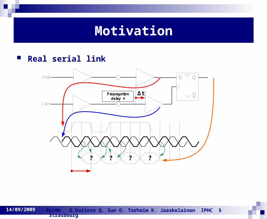
Motivation
Q
QSET
CLR
DData
Clock
Propagation delay ≠
Δt
Real serial link
? ? ? ?
614/09/2009 8b10b G.Doziere Q. Sun O. Torheim K. Jaaskelainen IPHC Strasbourg
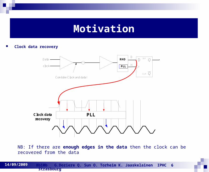
Motivation
Q
QSET
CLR
DData
clock
D
HPLL
RHD
Combine Clock and data!
Clock data recovery
PLLClock data recovery
NB: If there are enough edges in the data then the clock can be recovered from the data

714/09/2009 8b10b G.Doziere Q. Sun O. Torheim K. Jaaskelainen IPHC Strasbourg
Motivation
Code properties
Provide enough edges in the data to enable Clock Recovery
814/09/2009 8b10b G.Doziere Q. Sun O. Torheim K. Jaaskelainen IPHC Strasbourg
Motivation
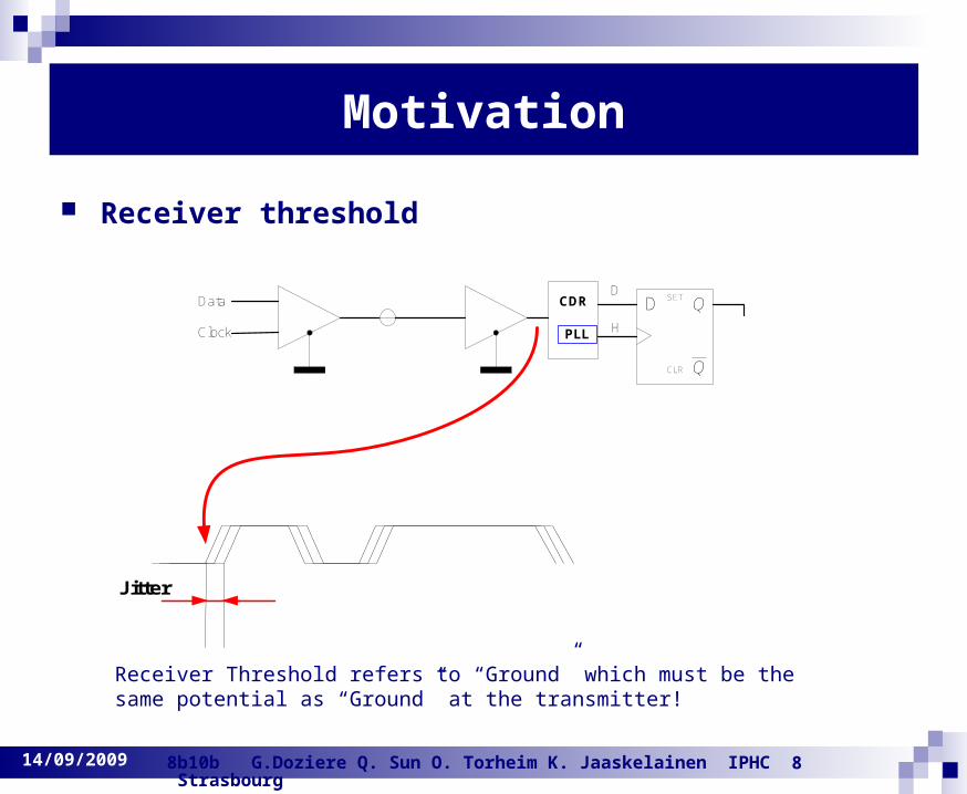
Q
QSET
CLR
DData
Clock
D
HPLL
CDR
Receiver threshold
Jitter
Receiver Threshold refers to “Ground” which must be the same potential as “Ground” at the transmitter!

914/09/2009 8b10b G.Doziere Q. Sun O. Torheim K. Jaaskelainen IPHC Strasbourg
Motivation
Q
QSET
CLR
DData
Clock
D
HPLL
CDR
Differential Link
Differential link
Receiver Threshold is halfway positive and negative signal
Use AC Coupling Capacitors…Need DC Balance!
NB: Common mode voltage difference between transmitter and termination at the receiver can result in excessive currents
1014/09/2009 8b10b G.Doziere Q. Sun O. Torheim K. Jaaskelainen IPHC Strasbourg
Motivation
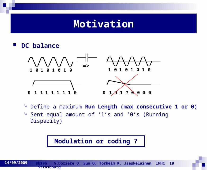
1 0 1 0 1 0 1 0=>
1 0 1 0 1 0 1 0
1 1 1 1 1 1 1 00
DC balance
Define a maximum Run Length (max consecutive 1 or 0) Sent equal amount of ‘1’s and ‘0’s (Running Disparity)
Modulation or coding ?
1 1 1 ? 0 0 0 00

1114/09/2009 8b10b G.Doziere Q. Sun O. Torheim K. Jaaskelainen IPHC Strasbourg
Motivation
Code Properties
Provide enough edges for Clock Recovery Maximum Run Length and DC Balance

1214/09/2009 8b10b G.Doziere Q. Sun O. Torheim K. Jaaskelainen IPHC Strasbourg
Coding 8b 10 b
Coding 8b 10b properties
8 bits to 10 bits conversion, (20 % overload of the data bandwidth) Input: 256 data characters ≠ , Output : 1024 characters ≠ including 12 specific control characters for the frame
synchronization (beginning and end of frame for ex)
Provide enough edges in the data for Clock Recovery,
DC Balance: running disparity positive or negative: ≠ between the number of 0 & 1 for each received byte, positive if nb of 1 > nb of 0, negative if not, possible values 0, +2, -2
run length : max length of identical successive values of 1 or 0 < 5
NB: coding develop by Wilmer & Franaszek (1983 patent expired from 2003)

1314/09/2009 8b10b G.Doziere Q. Sun O. Torheim K. Jaaskelainen IPHC Strasbourg
Coding 8b 10 b
byte (input coding)
7 6 5 4 3 2 1 0K
hi gi fi ei di ci bi ai0 1
K = 0 Þdata D
Control bit
4 3 2 1 0
ei di ci bi ai
7 6 5
hi gi fi
Decimal value Decimal value.K = 1 ÞControl K Decimal value Decimal value.
Input byte Notation
Ex: data bite 101 00110 => D6.5
control byte 110 10110 => K22.6
8 bits 10 bits (coding table cf. annexes)
4 3 2 1 0
ei di ci bi ai
7 6 5
hi gi fi
4 3 2 1 0
eo do co bo ao
5
io
8 7 6
ho go fo
9
jo
encoder 5 è 6 bits encoder 3 è 4 bits
K
0 1
256 values
1024 values : (all are not useful value) For most of the 256 (8B) values a positive and a negative 10B
value is selected depending on the “Current Running Disparity” (rd+ et rd-)
12 values/1024 “Special” K Characters (used word alignment)

1414/09/2009 8b10b G.Doziere Q. Sun O. Torheim K. Jaaskelainen IPHC Strasbourg
Coding 8b 10 b
Synchronization characters
The Comma characters K28.1/K28.5/K28.7 are used for frame synchronization
Create “ordered sets” – For example Fibre Channel Start Of Frame (SOF) = K28.5/D21.5/D23.0/D23.0 – K30.7 = Error Propagate – K28.3 = Carrier Extend

1514/09/2009 8b10b G.Doziere Q. Sun O. Torheim K. Jaaskelainen IPHC Strasbourg
Coding 8b 10 b
Main diagram
5b/6bEncoder:
ClassificationL functions
3b/4bEncoder:
ClassificationS function
ai
bi
ci
di
ei
fi
gi
hi
8 bits bus input port
Z(K/D)Control/
data
Encoder:Disparity &
Control
6 B bit control
4 B bit control
5b/6bEncoding
switch
3b/4bEncoding
switch
ai
bi
ci
di
ei
fi
gi
hi
ao
bo
co
do
eo
io
fo
go
ho
jo
Serializer 10 bits
Output line
Byte rate clock BYTECLK

1614/09/2009 8b10b G.Doziere Q. Sun O. Torheim K. Jaaskelainen IPHC Strasbourg
Architecture of prototype
Transmitter diagram
Clock generation: low jitter, power supply noise insensitive, JTAG configuration : 16 x 9 bits words, Data encoded read by JTAG., The chain check is done by serial data analyser, LVDS output.

1714/09/2009 8b10b G.Doziere Q. Sun O. Torheim K. Jaaskelainen IPHC Strasbourg
Implementation of Building Blocks
Encoder 8B/10B
Serializer•Load byte frequency: 16 MHz
•Bit output rate: 160 MHz
•Max. frequency DFF delay / loading of the input byte.
•Ring shifter register.
Coding implementing from an open source, currently estimated and studied
Clock Generator160 MHz PLL Cf. Isabelle Valin presentation
Buffer LVDS Frequency : 160 MHz, Termination Impedance: 100, Max differential swing: 400 mV, Common mode voltage : 1,2 V, A adjustable bias current flows between two single ended outputs, Typical current consumption: : 5,6 mA.

1814/09/2009 8b10b G.Doziere Q. Sun O. Torheim K. Jaaskelainen IPHC Strasbourg
Implementation of Building Blocks
Layout
AMS CMOS 0,35 μm Technology Total circuit area : 0,92 mm² integrated Independent test block integrated into the Mimosa 26 chip

1914/09/2009 8b10b G.Doziere Q. Sun O. Torheim K. Jaaskelainen IPHC Strasbourg
Results
Serial link LVDS at 160 MHz
Data eye is 60% opening at BER of 10-12(160 MHz) (measurement extrapolation)
Bit rate up to 250 Mbit/s The encoding data read by JTAG after decoding are the same of the initial
values (verilog & vhdl simulation test ) The data given by the serial data analyser correspond to the scheduled result. No intensive test has been achieved.

2014/09/2009 8b10b G.Doziere Q. Sun O. Torheim K. Jaaskelainen IPHC Strasbourg
Conclusion and perspectives
Serial transmission Coding 8b/10b with LVDS output
Block 8b/10b easily integrable in a design, Layout included in a area of 1450 μm x 330 μm, Consumption max. at 160 MHz < 10 mA, PLL working up to 300 MHz with a good noise immunity, LVDS Max. frequency (standalone) : 400 MHz New instigation to done for a frequency higher than 400 MHz
Serial link with Coding 8b/10b for optical fibre link
This block can also be used on a optical fibre link.
2114/09/2009 8b10b G.Doziere Q. Sun O. Torheim K. Jaaskelainen IPHC Strasbourg
Annexes References
1. A.X. Widmer and P.A. Franaszek, A DC-BALANCED, PARTITIONED-BLOCK, 8B/10B TRANSMISSION CODE, IBM Journal of Research and Development, Volume 27, Number 5, September 1983
1bis. Y. Takasaki, M. Tanaka, N. Maeda, K. Yamashita, and K. Nagano, “Optical Pulse Formats for Fiber Optic Digital Com- munications,” IEEE Trans. Commun. COM-24, 404-413 (1976).
2. J. M. Griffiths, “Binary Code Suitable for Line Transmission,” Electron. Lett. 5,79-81 (1969). 3. R. G. Kiwimagi, “Encoding/Decoding for Magnetic Record Storage Apparatus,” IBM Tech. Disclosure Bull. 18,
3147- 3149 (1976). 4. A. X. Widmer and P. A. Franaszek, “Transmission Code for High-speed Fibre-Optic Data Networks,” Electron.
Lett. 19, 5. P. A. Franaszek, “Sequence-State Coding for Digital Transmis- sion,”BellSyst. Tech. J. 47, 143-157 (1968). 6. P. A. Franaszek, “Sequence-State Methods for Run-Length- Limited Coding,” IBM J. Res. Develop. 14,376-383
(1970). 7. A. M. Patel, “Zero-Modulation Encoding in Magnetic Record- ing,” IBM J. Res. Develop. 19,366-378 (1975). 8. Peter A. Franaszek, “A General Method for Channel Coding,” IBM J. Res. Develop. 24,638-641 (1980). 9. P. A. Franaszek, “Construction of Bounded Delay Codes for Discrete Noiseless Channels,” IBM J. Res. Develop.
26, 506- 514 (1982). 10. B. Marcus, “Sofic Systems and Encoding Data on Magnetic Tape,” Preliminary Report, Notices, Amer. Math.
SOC. 29, 43 (1982). 11. R. L. Adler, D. Coppersmith, and M. Hassner, “Algorithms for Sliding Block Codes,” IEEE Trans. Info. Theory
IT-29, 5-22 (1983). 12. G. Nigel N. Martin, Glen G. Langdon, Jr., and Stephen J. P. Todd, “Arithmetic Codes for Constrained
Channels,” IBM J. Res. Develop. 27,94-I06 (1983). 13. Ta-Mu Chien, “Upper Bound on the Efficiency of DC- Constrained Codes,’’ Bell Syst. Tech. J. 49, 2261-2287
(1970). 14. J. J. Stiffler, “Theory of Synchronous Communications,” Pren- tice-Hall, Inc., Englewood Cliffs, NJ, 1971, pp.
368-372.

2214/09/2009 8b10b G.Doziere Q. Sun O. Torheim K. Jaaskelainen IPHC Strasbourg
Annexes Coding block diagram8b/10b (1/6)
The FIG. 3 shows the digital schematic of the Classification .5B/6B ": functions L “

2314/09/2009 8b10b G.Doziere Q. Sun O. Torheim K. Jaaskelainen IPHC Strasbourg
Annexes Coding block diagram8b/10b (2/6)
The FIG.4 shows the digital schematic of the Classification 3B/4B ": functions S “
(1/ )
2414/09/2009 8b10b G.Doziere Q. Sun O. Torheim K. Jaaskelainen IPHC Strasbourg
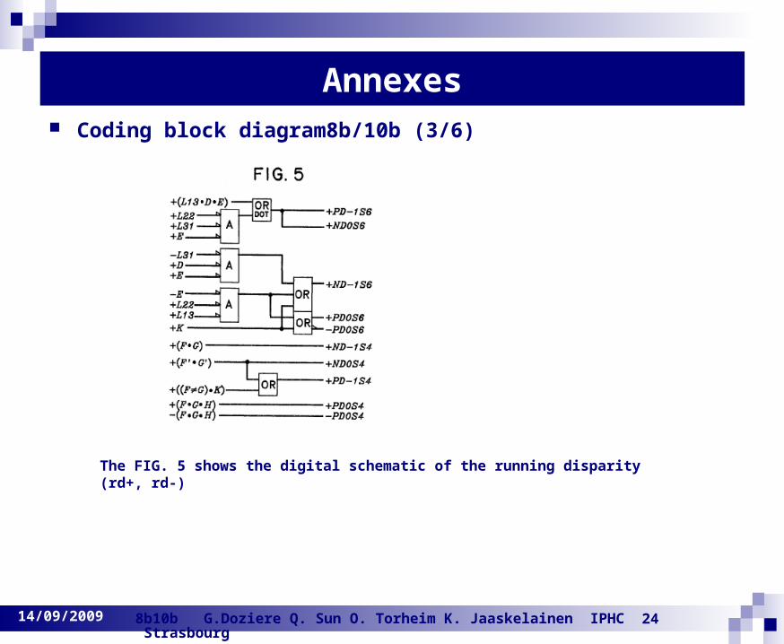
Annexes Coding block diagram8b/10b (3/6)
The FIG. 5 shows the digital schematic of the running disparity (rd+, rd-)

2514/09/2009 8b10b G.Doziere Q. Sun O. Torheim K. Jaaskelainen IPHC Strasbourg
Annexes Coding block diagram8b/10b (4/6)
The FIG. 6 shows the digital schematic of the complementation control

2614/09/2009 8b10b G.Doziere Q. Sun O. Torheim K. Jaaskelainen IPHC Strasbourg
Annexes Coding block diagram8b/10b (5/6)
The FIG. 7 shows the digital schematic of 5b/6b terminal.

2714/09/2009 8b10b G.Doziere Q. Sun O. Torheim K. Jaaskelainen IPHC Strasbourg
Annexes Coding block diagram8b/10b (6/6)
The FIG. 8 shows the digital schematic of 3b/4b terminal.

2814/09/2009 8b10b G.Doziere Q. Sun O. Torheim K. Jaaskelainen IPHC Strasbourg
Annexes Running disparity coding table (1/4)

2914/09/2009 8b10b G.Doziere Q. Sun O. Torheim K. Jaaskelainen IPHC Strasbourg
Annexes Running disparity coding table (2/4)

3014/09/2009 8b10b G.Doziere Q. Sun O. Torheim K. Jaaskelainen IPHC Strasbourg
Annexes Running disparity coding table (3/4)

3114/09/2009 8b10b G.Doziere Q. Sun O. Torheim K. Jaaskelainen IPHC Strasbourg
Annexes Running disparity coding table (4/4)

3214/09/2009 8b10b G.Doziere Q. Sun O. Torheim K. Jaaskelainen IPHC Strasbourg
Annexes 12 “Special” K Characters
CommaCharacters“The only patterns thathave 5 consecutive‘1’s or ‘0’s

3314/09/2009 8b10b G.Doziere Q. Sun O. Torheim K. Jaaskelainen IPHC Strasbourg
Annexes Decoding 6b/5b

3414/09/2009 8b10b G.Doziere Q. Sun O. Torheim K. Jaaskelainen IPHC Strasbourg
Annexes
Decoding 4b/3b

3514/09/2009 8b10b G.Doziere Q. Sun O. Torheim K. Jaaskelainen IPHC Strasbourg
Annexes
Test diagram
Evaluation board
Power supply
Signal generator 10 MHz
Serial data analyser
JTAG
ASIC
// Port