A Screening Method Using Infrared Imaging to Detect ... · A Screening Method Using Infrared...
34
A Screening Method Using Infrared Imaging to Detect Pattern Defects in Foil and Thin Film Resistors Lyudmyla Panashchenko/NASA Goddard Space Flight Center Jay Brusse/ASRC AS&D at NASA Goddard Space Flight Center Matthew King-Smith/The College of Wooster Presented by Lyudmyla Panashchenko at the 2015 Components for Military and Space Electronics (CMSE) Conference and Exhibition, Los Angeles, CA, March 1-3, 2015. 1
Transcript of A Screening Method Using Infrared Imaging to Detect ... · A Screening Method Using Infrared...

A Screening Method Using Infrared Imaging
to Detect Pattern Defects in Foil and Thin Film Resistors
Lyudmyla Panashchenko/NASA Goddard Space Flight Center
Jay Brusse/ASRC AS&D at NASA Goddard Space Flight Center
Matthew King-Smith/The College of Wooster
Presented by Lyudmyla Panashchenko at the 2015 Components for Military and Space Electronics (CMSE) Conference and Exhibition, Los Angeles, CA, March 1-3, 2015.
1
Acronyms
Al-N = aluminum nitride
InSb = Indium Antimonide
NEPP = NASA Electronic Parts & Packaging (NEPP) Program
NiCr = Nichrome
Presented by Lyudmyla Panashchenko at the 2015 Components for Military and Space Electronics (CMSE) Conference and Exhibition, Los Angeles, CA, March 1-3, 2015.
2

A Case for an Improved Screening Method: System-Level Resistor Failure
• During system-level testing, a NASA program experienced an intermittent open circuit failure of a surface mount Nichrome (NiCr) foil resistor
• Failure analysis identified a fracture in the resistor foil with a non-conductive aluminum nitride (Al-N) particle embedded in the NiCr foil at the failure site
• The particle significantly reduced the cross sectional area of the resistor line leading to ‘hot spot’ generation during powered operation
• Power cycling lead to thermomechanical fatigue fracture of the localized constriction
• Standard part-level screening practices (e.g., short time overload) failed to detect this flawed resistor
Presented by Lyudmyla Panashchenko at the 2015 Components for Military and Space Electronics (CMSE) Conference and Exhibition, Los Angeles, CA, March 1-3, 2015.
3

A Case for an Improved Screening
Method: Embedded Al-N Particle in Foil Resistor Size 1206, 30
kΩ
Presented by Lyudmyla Panashchenko at the 2015 Components for Military and Space Electronics (CMSE) Conference and Exhibition, Los Angeles, CA, March 1-3, 2015.
4
Aluminum Nitride Particle
10 um 1 um
NiC
r
NiC
r
NiC
r
NiC
r
NiC
r
Fractured NiCr Gridline With Embedded Al-N Particle

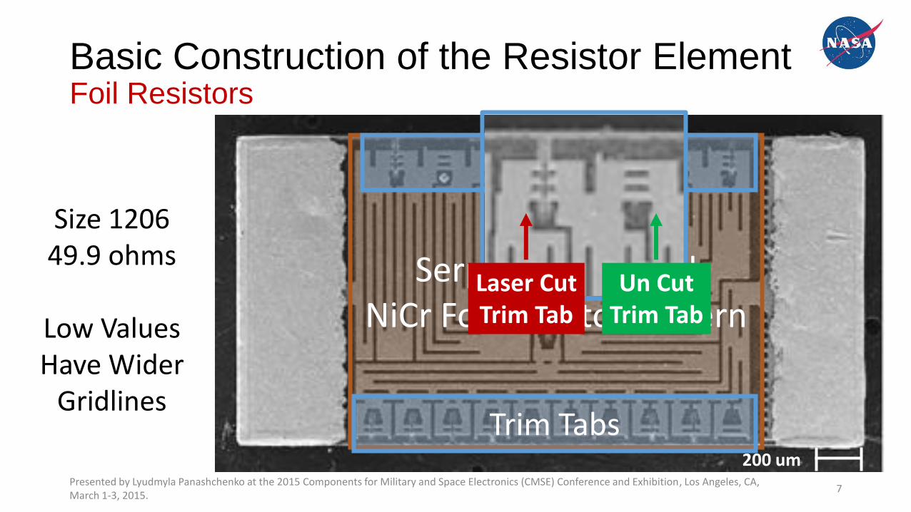
Basic Construction of the Resistor Element Foil Resistors
• Resistor Material
• NiCr-based alloy is rolled into foil sheets
• Foil thickness is typically 2 – 5 microns
• Photolithography
• Serpentine patterns are etched into the nichrome foil sheet
• Etched line widths may be as narrow as a few microns.
• Resistor pattern consists of series and parallel resistor segments
• Trim tabs built into pattern allow precise resistance adjustment
• Bonding Resistor Element to Substrate
• NiCr foil is adhesively bonded to an alumina substrate
• Trimming to Value
• Laser (or mechanical scribe) is used to selectively cut trim tabs
• Protective Coatings
• Polymeric coatings encapsulate the resistor element
Presented by Lyudmyla Panashchenko at the 2015 Components for Military and Space Electronics (CMSE) Conference and Exhibition, Los Angeles, CA, March 1-3, 2015.
5
Foil Resistor with External Protective Coatings Removed
200 um

Basic Construction of the Resistor Element Foil Resistors
Presented by Lyudmyla Panashchenko at the 2015 Components for Military and Space Electronics (CMSE) Conference and Exhibition, Los Angeles, CA, March 1-3, 2015.
6
Size 1206 49.9 ohms
Low Values Have Wider
Gridlines
200 um
Basic Construction of the Resistor Element Foil Resistors
Presented by Lyudmyla Panashchenko at the 2015 Components for Military and Space Electronics (CMSE) Conference and Exhibition, Los Angeles, CA, March 1-3, 2015.
7
Size 1206 49.9 ohms
Low Values Have Wider
Gridlines
200 um
Serpentine Etched NiCr Foil Resistor Pattern
Trim Tabs
Trim Tabs
Un Cut Trim Tab
Laser Cut Trim Tab

Basic Construction of the Resistor Element Foil Resistors
Presented by Lyudmyla Panashchenko at the 2015 Components for Military and Space Electronics (CMSE) Conference and Exhibition, Los Angeles, CA, March 1-3, 2015.
8
Size 1206 20,000 ohms
High Values
Have Narrower Gridlines
200 um

Basic Construction of the Resistor Element Cross Section of a Surface Mount Foil Resistor
Overview Cross Section
Presented by Lyudmyla Panashchenko at the 2015 Components for Military and Space Electronics (CMSE) Conference and Exhibition, Los Angeles, CA, March 1-3, 2015.
9
Opaque Coating (10-20um)
Polymer Coating (~10um)
Resistor Foil (2-5um)
Adhesive (~5um)
Alumina Substrate
Ti, O
Al, O
C, O
Ni, Cr
C, S
Al, O
10 um

Traditional Resistor Screening Methods Optical Microscopy
Presented by Lyudmyla Panashchenko at the 2015 Components for Military and Space Electronics (CMSE) Conference and Exhibition, Los Angeles, CA, March 1-3, 2015.
10
Void > 75% in Foil Resistor Bridge < 10% in Foil Resistor
Thin Film (MIL-PRF-55342) Foil Resistors
Test Conditions 30x to 60x optical microscopy prior to encapsulation
Sample Size 100% in-process screen 100% high reliability products only
Rejection Criteria Voids > 50% nominal line width Bridges < 50% smallest line width
Voids > 75% nominal line width Bridges < 10% smallest line width

Traditional Resistor Screening Methods Short Time Overload
It is claimed that this test will force failure of devices with the most severe pattern constrictions
Presented by Lyudmyla Panashchenko at the 2015 Components for Military and Space Electronics (CMSE) Conference and Exhibition, Los Angeles, CA, March 1-3, 2015.
11
Thin Film (MIL-PRF-55342) Foil Resistors
Test Conditions 6.25x rated power for 5 seconds
Sample Size 20 pcs (space level only) 10 pcs (high reliability products)
Rejection Criteria ΔR > 0.1% ΔR > 0.02%

Traditional Resistor Screening Methods Power Conditioning (Also referred to as Burn-In)
Presented by Lyudmyla Panashchenko at the 2015 Components for Military and Space Electronics (CMSE) Conference and Exhibition, Los Angeles, CA, March 1-3, 2015.
12
Thin Film (MIL-PRF-55342) Foil Resistors
Test Conditions 1.5x rated power for 100 hours at 70°C
Sample Size 100% (space level only) 100% (high reliability products only)
Rejection Criteria ΔR > 0.2% ΔR > 0.03%
It is claimed that this test will force failure of devices with the most severe pattern constrictions

Resistor Pattern Defects Constrictions (Voids)
Presented by Lyudmyla Panashchenko at the 2015 Components for Military and Space Electronics (CMSE) Conference and Exhibition, Los Angeles, CA, March 1-3, 2015.
13
Low Current Density
High
Low Current Density
Hot Spot
Resistors with these Defects Found By End User Despite Having Been Subjected to Traditional Screening

Resistor Pattern Defects Narrow Bridges
Presented by Lyudmyla Panashchenko at the 2015 Components for Military and Space Electronics (CMSE) Conference and Exhibition, Los Angeles, CA, March 1-3, 2015.
14
Hot Spot
Resistors with these Defects Found By End User Despite Having Been Subjected to Traditional Screening

Resistor Pattern Defects Embedded Particles
Presented by Lyudmyla Panashchenko at the 2015 Components for Military and Space Electronics (CMSE) Conference and Exhibition, Los Angeles, CA, March 1-3, 2015.
15
HIG
H
Low
C
urre
nt
De
nsity
Hot Spot
Resistors with these Defects Found By End User Despite Having Been Subjected to Traditional Screening
Low
C
urre
nt
De
nsity

Resistor Pattern Defects Potential Effects of “Constrictions” in Resistor Lines
• Localized constriction in the resistor pattern will result in higher current density and ‘hot spot’ formation due to Joule heating during powered operation
• Localized constrictions are more prone to fracture especially during power cycling • Failure Mechanism = thermomechanical fatigue fracture • Failure Modes = open circuit or shift in resistance
• ‘Hot spots’ can also cause thermal decomposition of protective coatings and adhesives (> ~300°C) whose byproducts may accelerate failure
• Failure Mechanism = stress corrosion cracking of resistor element + thermomechanical fatigue fracture
• Failure Mode = open circuit or shift in resistance
Presented by Lyudmyla Panashchenko at the 2015 Components for Military and Space Electronics (CMSE) Conference and Exhibition, Los Angeles, CA, March 1-3, 2015.
16

Resistor Pattern Defects A Model of Joule Heat Propagation at Local Constriction
Thermal Diffusion Simulated Slice in Resistor Line Reducing Width by 90% (i.e. 10% remaining)
Presented by Lyudmyla Panashchenko at the 2015 Components for Military and Space Electronics (CMSE) Conference and Exhibition, Los Angeles, CA, March 1-3, 2015.
17

New Screening Method for Resistor Pattern Defects High Resolution Infrared Thermography During Power Pulsing
1. Examine resistor using high resolution infrared camera able to resolve features ~10 um or smaller
2. Apply brief power pulses (a few pulses are sufficient) • For example, 6.25x rated power, 50 ms, 10% duty cycle • Brief pulses dynamically confine the Joule heating to the “local constrictions” in the pattern • Brief duty cycle allows resistor to cool to ambient conditions before subsequent pulse
3. Analyze infrared images for localized “hot spots” within the pattern • Hot spots are indicative of constrictions (e.g., voids, bridges, embedded particles)
4. A conservative criteria: Reject parts exhibiting significant “hot spots”
Presented by Lyudmyla Panashchenko at the 2015 Components for Military and Space Electronics (CMSE) Conference and Exhibition, Los Angeles, CA, March 1-3, 2015.
18

Detector Type Indium Antimonide (InSb)
Spectral Range 3.0 - 5.0 µm
Resolution ~4µm
Frame Rate Up to 132 Hz (frames per second)
Standard Temperature Range
-20°C to 500°C (-4°F to 932°F)
Accuracy ±2°C or ±2% of Reading
Presented by Lyudmyla Panashchenko at the 2015 Components for Military and Space Electronics (CMSE) Conference and Exhibition, Los Angeles, CA, March 1-3, 2015.
19
New Screening Method for Resistor Pattern Defects High Resolution Infrared Camera with 4x lens option

New Screening Method for Resistor Pattern Defects Comparison of Two Different Infrared Cameras The same resistor having 2 constriction defects is examined FLIR SC660 with 25 micron detector pitch FLIR SC8300HD with 4 micron detector pitch
Presented by Lyudmyla Panashchenko at the 2015 Components for Military and Space Electronics (CMSE) Conference and Exhibition, Los Angeles, CA, March 1-3, 2015.
20
1 hot spot detected?

New Screening Method for Resistor Pattern Defects High Resolution Infrared Camera Identifies Hot Spots During Powered Operation
Presented by Lyudmyla Panashchenko at the 2015 Components for Military and Space Electronics (CMSE) Conference and Exhibition, Los Angeles, CA, March 1-3, 2015.
21
Bridge Defect
Void Defect

Infrared Video Demonstration 2kΩ Foil Resistor; Size 1206; Ten 50 ms pulses at 6.25x Rated Power
Presented by Lyudmyla Panashchenko at the 2015 Components for Military and Space Electronics (CMSE) Conference and Exhibition, Los Angeles, CA, March 1-3, 2015.
22
Constriction

Optical Image Infrared Image Using FLIR SC8300 Camera with spectral range 1.5 to 5.0 microns
23
Infrared Image of UNPOWERED
Resistor
This feature enables use of this technique as a post-procurement screening inspection
New Screening Method for Resistor Pattern Defects The Protective Coatings are Transmissive at These Infrared Wavelengths
To be presented by Lyudmyla Panashchenko at the 2015 Components for Military and Space Electronics (CMSE) Conference and Exhibition, Los Angeles, CA, March 1-3, 2015. Presented by Lyudmyla Panashchenko at the 2015 Components for Military and Space Electronics (CMSE) Conference and Exhibition, Los Angeles, CA, March 1-3, 2015.

Example Inspection with New Method Foil Resistor with Multiple Bridge Defects as Seen in Infrared Applying 6.25x Rated Power for 50 ms pulses; 10% duty cycle
Presented by Lyudmyla Panashchenko at the 2015 Components for Military and Space Electronics (CMSE) Conference and Exhibition, Los Angeles, CA, March 1-3, 2015.
24
Inspection Performed Without Removing Resistor Protective
Coatings

Presented by Lyudmyla Panashchenko at the 2015 Components for Military and Space Electronics (CMSE) Conference and Exhibition, Los Angeles, CA, March 1-3, 2015.
25
Example Inspection with New Method Foil Resistor with Two Bridge Defects as Seen in Infrared Applying 6.25x Rated Power for 50 ms pulses; 10% duty cycle
Inspection Performed Without Removing Resistor Protective
Coatings

Presented by Lyudmyla Panashchenko at the 2015 Components for Military and Space Electronics (CMSE) Conference and Exhibition, Los Angeles, CA, March 1-3, 2015.
26
Example Inspection with New Method Foil Resistor with Two Local Constriction Defects as Seen in Infrared Applying 6.25x Rated Power for 50 ms pulses; 10% duty cycle
Inspection Performed Without Removing Resistor Protective
Coatings

Presented by Lyudmyla Panashchenko at the 2015 Components for Military and Space Electronics (CMSE) Conference and Exhibition, Los Angeles, CA, March 1-3, 2015.
27
Example Inspection with New Method Foil Resistor with One Local Constriction Defect as Seen in Infrared Applying 6.25x Rated Power for 50 ms pulses; 10% duty cycle
Inspection Performed Without Removing Resistor Protective
Coatings

Presented by Lyudmyla Panashchenko at the 2015 Components for Military and Space Electronics (CMSE) Conference and Exhibition, Los Angeles, CA, March 1-3, 2015.
28
Example Inspection with New Method Foil Resistor with One Local Constriction Defect as Seen in Infrared Applying 6.25x Rated Power for 50 ms pulses; 10% duty cycle
Inspection Performed Without Removing Resistor Protective
Coatings

Conclusions • NASA has developed a method to detect pattern defects in foil and thin film
resistors using high resolution infrared thermography while applying brief power pulses
• The technique can be used at various stages: • In-process screen by resistor manufacturer prior to protective coating application
• Post-procurement screen by end user if coatings are transmissive at infrared wavelengths
• Destructive physical analysis and failure analysis
Future Work • NASA plans to evaluate reliability of suspect parts identified by this method
• Long-term life test comparison of suspect vs. non-suspect parts
Presented by Lyudmyla Panashchenko at the 2015 Components for Military and Space Electronics (CMSE) Conference and Exhibition, Los Angeles, CA, March 1-3, 2015.
29
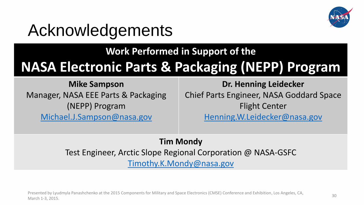
Acknowledgements
Presented by Lyudmyla Panashchenko at the 2015 Components for Military and Space Electronics (CMSE) Conference and Exhibition, Los Angeles, CA, March 1-3, 2015.
30
Work Performed in Support of the
NASA Electronic Parts & Packaging (NEPP) Program Mike Sampson
Manager, NASA EEE Parts & Packaging (NEPP) Program
Dr. Henning Leidecker Chief Parts Engineer, NASA Goddard Space
Flight Center [email protected]
Tim Mondy Test Engineer, Arctic Slope Regional Corporation @ NASA-GSFC

Backup Slides
Presented by Lyudmyla Panashchenko at the 2015 Components for Military and Space Electronics (CMSE) Conference and Exhibition, Los Angeles, CA, March 1-3, 2015.
31

• Resistor Material
• Typically a NiCr or Tantalum Nitride-based alloy sputter deposited onto an alumina substrate
• Film thickness typically 50 nm to 250 nm
• Photolithography
• Serpentine patterns are etched into the thin film
• Etched line widths as narrow as a few microns
• Pattern consists of both series and parallel resistor segments
• Coarse, Intermediate and fine adjustment pattern features are built into the pattern
• Trimming to Value
• Laser is used to selectively remove thin film resistor material
• Protective Coatings
• Polymeric coatings encapsulate the resistor element
Presented by Lyudmyla Panashchenko at the 2015 Components for Military and Space Electronics (CMSE) Conference and Exhibition, Los Angeles, CA, March 1-3, 2015.
32
Basic Construction of the Resistor Element Thin Film Resistors

Example Inspection with New Method Thin Film Resistors as Seen in Infrared Applying 6.25x Rated Power for 100 ms pulses; 10% duty cycle
Presented by Lyudmyla Panashchenko at the 2015 Components for Military and Space Electronics (CMSE) Conference and Exhibition, Los Angeles, CA, March 1-3, 2015.
33
Inspection Performed Without Removing Resistor Protective
Coatings

34
Example Inspection with New Method Thin Film Resistors as Seen in Infrared Applying 6.25x Rated Power for 100 ms pulses; 10% duty cycle
Inspection Performed Without Removing Resistor Protective
Coatings
Presented by Lyudmyla Panashchenko at the 2015 Components for Military and Space Electronics (CMSE) Conference and Exhibition, Los Angeles, CA, March 1-3, 2015.