A Review on Single CFA based Multifunctional Network for ...
10
International Journal of Electronic and Electrical Engineering. ISSN 0974-2174 Volume 4, Number 1 (2011), pp.33-42 © International Research Publication House http://www.irphouse.com A Review on Single CFA based Multifunctional Network for Analog Signal Processing Indu Prabha Singh 1 and Kalyan Singh 2 1 Deptt. of Electronics and Comm. Engg. SITM, Unnao-209859, India 2 Dept. of Physics and Electronics Engg. , Dr. R.M.L. Avadh University, Faizabad, India E-mail: [email protected], [email protected]. Abstract This paper presents a review of multifunctional network utilizing a current feedback amplifier (CFA-AD 844) as a basic building block. The circuit implements the functions of integrator/ differentiator, high-pass, low-pass and band-pass on the same topology with the appropriate design. The circuits have been analyzed, simulated and experimentally tested. The simulation and experimental results verify the performance of the reported circuits in terms of the number of basic building blocks used and high selectivity. It has also been examined that the variation of the time constant (T) of CFA based multifunction network, the quality factor (Q) of integrators/ differentiators and filter may be measured with single component variation at extended frequency ranges (1–30 MHz). Index Terms: Current feedback amplifier (CFA), Integrator, Differentiator, Filters. Introduction Current-mode active elements offer the main advantages like greater linearity, low power consumption and wider bandwidth over their voltage-mode counter parts [1-3]. Also, the design of filter circuits employing current-mode active elements may be used in phase-locked loop frequency modulation (FM), stereo demodulators, touch- tone telephone and cross over networks used in a three-way high fidelity loudspeaker [4]. Second-order active filters with infinite input impedance are of great interest because several networks of that kind can be directly connected in cascade to implement higher order filters [5-8] with no need to interpose active separating stages.
Transcript of A Review on Single CFA based Multifunctional Network for ...
International Journal of Electronic and Electrical Engineering. ISSN 0974-2174 Volume 4, Number 1 (2011), pp.33-42 © International Research Publication House http://www.irphouse.com
A Review on Single CFA based Multifunctional Network for Analog Signal Processing
Indu Prabha Singh1 and Kalyan Singh2
1Deptt. of Electronics and Comm. Engg. SITM, Unnao-209859, India
2Dept. of Physics and Electronics Engg. , Dr. R.M.L. Avadh University, Faizabad, India
E-mail: [email protected], [email protected].
Abstract
This paper presents a review of multifunctional network utilizing a current feedback amplifier (CFA-AD 844) as a basic building block. The circuit implements the functions of integrator/ differentiator, high-pass, low-pass and band-pass on the same topology with the appropriate design. The circuits have been analyzed, simulated and experimentally tested. The simulation and experimental results verify the performance of the reported circuits in terms of the number of basic building blocks used and high selectivity. It has also been examined that the variation of the time constant (T) of CFA based multifunction network, the quality factor (Q) of integrators/ differentiators and filter may be measured with single component variation at extended frequency ranges (1–30 MHz).
Index Terms: Current feedback amplifier (CFA), Integrator, Differentiator, Filters.
Introduction Current-mode active elements offer the main advantages like greater linearity, low power consumption and wider bandwidth over their voltage-mode counter parts [1-3]. Also, the design of filter circuits employing current-mode active elements may be used in phase-locked loop frequency modulation (FM), stereo demodulators, touch-tone telephone and cross over networks used in a three-way high fidelity loudspeaker [4]. Second-order active filters with infinite input impedance are of great interest because several networks of that kind can be directly connected in cascade to implement higher order filters [5-8] with no need to interpose active separating stages.
34 Indu Prabha Singh and Kalyan Singh
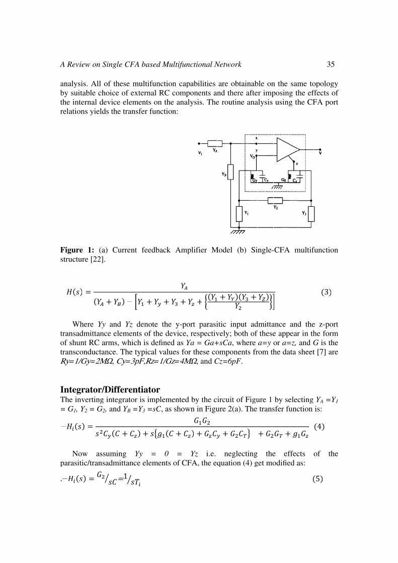
Infinite input impedance cells assure a total uncoupling between the different elementary stages. This will entail an easier determination of the passive component values of each of the elementary cells and an easier to design a global circuit. In such circuits theoretical and experimental frequency responses of the filters will generally be closer. Frequency response of recently available Current feedback amplifier [9-12] device- AD 844 remains unchanged up to some hundred of megahertz when they are used to the design of different kind of filters. The AD844 is free from the slew rate limitations inherent in traditional op amps and other current-feedback op amps. Peak output rate of change can be over 2000 V/µs for a full 20 V output step. Settling time is typically 100 ns to 0.1%, and essentially independent of gain. The AD844 can drive 50 Ω loads to ±2.5 V with low distortion and exhibits excellent differential gain and differential phase characteristics, making it suitable for a variety of video applications with bandwidths up to 60 MHz. The literature presents different filters [13-19], integrators [20, 21] schemes using CFAs and external discrete RC components. This paper presents a review of the multifunctional network that can perform the function of integrator/differentiator and filter by employing only a single CFA and few passive components [22]. Here, we have utilized the CFA (AD-844): analog device parasitic/transimpedance, for the realization of different functions. The effects of the parasitic elements in determining the quality (Q) of the integrator/differentiator had been examined. Then, we describe the design of high-quality (Q) selective filters. All of these multifunction capabilities are obtainable on the same topology after suitable choice of external RC components. Circuit Analysis The block diagram of the CFA is shown in Figure 1(a), and its terminal relations are given by:
1 0 00 0 00 0 1
(1)
The Inverting/Non-inverting input terminal of CFA is actually the output/input of the unity gain buffer, which ideally has zero output impedance and infinite input impedance. As a result, the input impedance at the inverting terminal is zero whereas the input impedance at the non-inverting terminal is infinite. The output is therefore a linear, current-controlled source with zero output impedance.
. 2
Where z (s) is the trans-impedance parameter (in ohms), iinv is the current flowing out of the inverting input terminal. The reported circuit [22] is shown in Figure 1(b). The circuit uses one current-feedback amplifier and five admittances. For the realization of integrator/differentiator and filter, device parasitic/ transimpedance are utilized in
A
anbthre
Fst
trotrR InT=
p
.
A Re
naly she elat
Figutru
Wranf shran
Ry=
ntThe= G
Nara
evi
lyssuitinttio
urectu
Whnsadhu
nsco=1/
ege inG1,
Noasit
iew
is. tabternons
e 1ure
herdmnt ond/Gy
granveY2
ow tic/
w on
Able nalyie
1: [2
re mitt
RCducy=2
atoertin =
a/tra
n S
All och
l deeld
(a22].
Yyanc
C acta2M
or/ng G2
assans
Sin
of hoicevids t
a) .
y ace
armanc
MΩ,
/Diint
2, a
sumsad
gle
thece ice the
Cu
andele
ms, e. T
Ω, C
iffeteg
and
mindmi
=
e C
eseof el
e tra
urre
d YemwhTh
Cy=
eregratd YB
ng itta
=
CFA
e mex
emans
ent
Yz ment
hiche t=3p
entorB =
Yanc
A b
mulxter
mensfe
t fe
dents o
ch ityppF,
ntiar is
=Y3
Yy e e
bas
ltifurna
nts r fu
eed
notof is d
pica,Rz
ato im
3 =s
=elem
ed
uncal Ronunc
dba
te the
defial vz=1
or mplsC
= me
M
ctioRCn thctio
ack
thee dfinevalu1/G
lem
C, a
0 ents
Mult
on C cohe aon:
k A
e ydeved ues
Gz=
mens sh
s o
tifu
caomana:
Am
y-piceas s fo
=4M
nteho
= f C
unc
apampo
aly
mpl
pore, rYaor
4MΩ
d bwn
YCFA
ctio
abiloneysis
lifie
t prespa =theΩ, a
by n in
Yz A,
ona
litientss. T
er
parpec
= Geseand
then F
i.the
al N
es s anThe
M
rasictiv
Ga+e cod C
e cFigu
.e. e eq
Net
arend e ro
Mod
iticvel+sComCz=
ircure
nqua
two
e oth
out
del
c inly; Ca,
mpo=6p
cuite 2(
negatio
ork
obtheretine
(b
npubo
, wonepF
t of(a)
gleon
k
aine ae a
b)
ut oth whe
nts.
f F. T
ecti(4
nabafteana
Si
adof
ere s fr
FiguThe
ing4) g
ble er ialys
ing
dmif tha=
rom
uretra
g get
onmpsis
gle-
ittahese=y m th
e 1 ans
themo
n thposus
-CF
ance aor he
bysfer
e odi
he singsing
FA
ce appa=da
y ser fu
efifie
samg tg th
A m
anpear=z, ata
eleunc
ffeced a
methe he
mul
d tr inanshe
ctinctio
cts as:
e toefCF
ltif
then thnd Geet
ng on
opoffecFA
fun
e zhe G it [7
YA
is:
of
3
olocts
A po
ncti
z-poforis t7] a
A =
t
35
ogyof
ort
ion
ortrmtheare
=Y1
the
y f t
n
t m e e
e
3
T
(
bT
Y
6
The
(a)
y sThe
FY3 =
N
e tim
W
Th
Ansime co
Th
Fo= G
No
me
ith
he q
n almplyorre
he q
or aG2,
ow
e co
h tim
qua
ltery resp
qua
an ian
by
ons
me
alit
rnareppon
alit
invnd Y
y ig
stan
e co
ty f
ate lac
ndi
ty f
vertY2
gno
nt i
ons
fac
invcingng
fac
tin= s
orin
is i
stan
tor
verg G ex
tor
g dsC,
ng
ind
nt T
r fo
rtinG1 xpr
r fo
diff, w
Yy
dep
Ti=
F
or i
ng by
ress
or i
ferwhic
y an
end
=CR
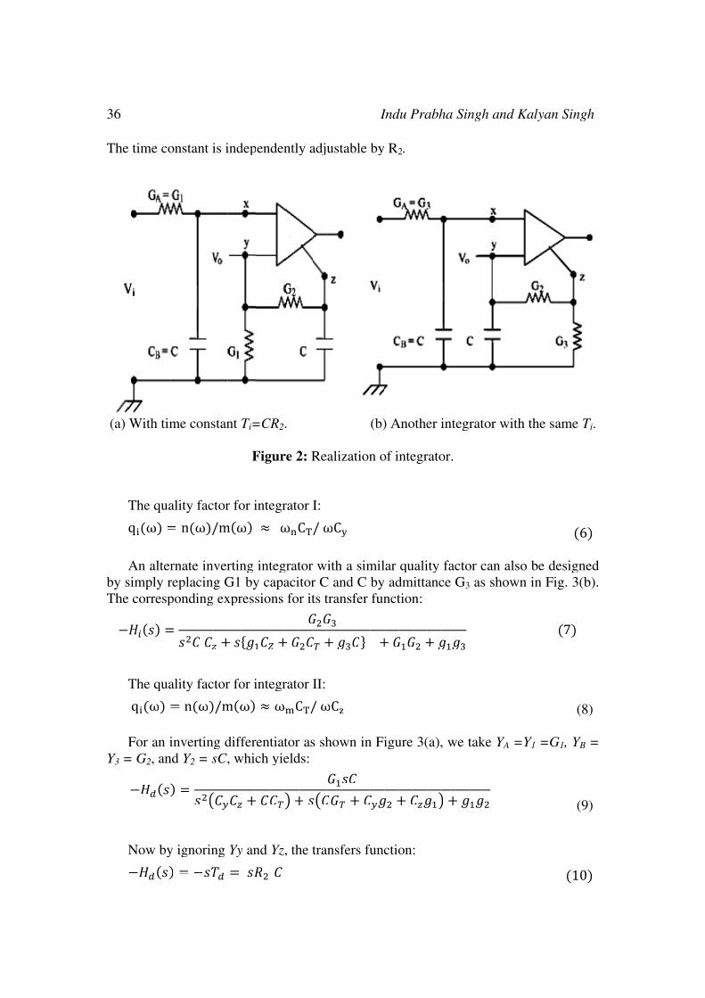
Fig
inte
inty casio
inte
entch
nd
den
CR2.
gur
egr
tegapans
egr
tiatyie
Yz,
ntly
.
re 2
rato
gratacifor
rato
toreld
, th
y a
2: R
or I
/
tor itorr it
or I
r asds:
he t
adju
Rea
I:
/
wir Cts t
II:
s sh
tran
ust
aliz
ithC antran
how
nsf
tab
zat
h a nd nsf
wn
fer
ble
tion
simC
fer
n in
s fu
I
by
(b)
n o
milbyfun
n Fi
unc
Ind
R2
) A
of i
ar adnct
igu
ctio
du P
2.
Ano
nte
qudmtion
ure
on
Pra
othe
egr
ualiittan:
3(
:
abh
er i
rato
ity anc
(a),
ha
int
or.
facce G
, w
Sin
egr
ctoG3
we t
ngh
rat
or cas
tak
h a
or
cans sh
ke Y
and
wi
n alhow
YA
d Ka
ith
lsown
=Y
Kaly
the
bein
Y1 =
yan
e sa
e dn Fi
=G
n Si
am
esiig.
G1,
(
ing
me T
(6
ign3(b
(8
YB
(9
(10
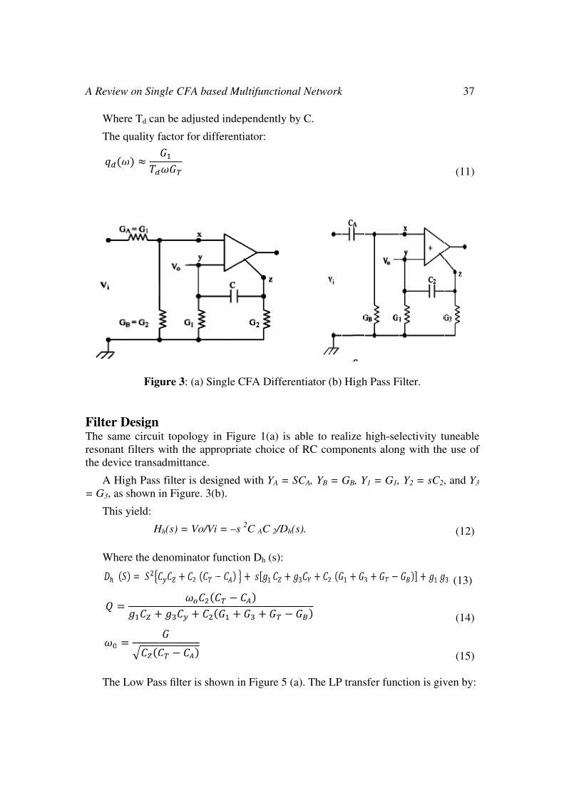
gh
Ti.
6)
nedb).
8)
B =
9)
0)
d
A
FTreth
=
A Re
W
FiltTheesohe d
= G
W
evi
Wh
Th
tere saonadev
A G3,
Th
Wh
Th
iew
her
he q
r Damant vic
Hias
his
her
he L
w on
re T
qua
Desme c
filce t
gh sho
yie
re t
Low
n S
Td
alit
F
sigcircltertran
Paow
eld
the
w P
Sin
can
ty f
Fig
gn cuirs wnsa
asswn i
:
H
e de
Pas
gle
n b
fac
ur
it twitadm
s filin F
Hh(s
eno
ss fi
e C
be a
tor
re 3
topth tmit
lterFig
s) =
om
filt
CFA
adj
r fo
3: (
polothettan
r isgur
= V
mina
ter
A b
jus
or d
(a)
ogye apnce
s dre.
Vo/
ato
is s
bas
ted
diff
Sin
y inppr
e.
desi3(b
/Vi
or f
sho
ed
d in
fer
ngl
n Frop
ignb).
i =
fun
ow
M
nde
rent
le C
Figpria
ned
–s
cti
wn i
Mult
epe
tiat
CF
gurate
d w
s 2C
on
in F
tifu
end
tor
FA
re 1e ch
with
C A
Dh
Fig
unc
den
r:
Di
1(ahoi
h YA
C 2
h (s
gur
ctio
ntly
iffe
a) iice
YA =
2/D
s):
e 5
ona
y by
eren
is ae of
= S
Dh(s
5 (a
al N
y C
nti
ablf R
SCA
s).
a).
Net
C.
ato
le tRC
A, Y
Th
two
or (
to co
YB
he L
ork
(b)
reaomp
=
LP
k
Hi
alizpon
GB
tra
igh
ze nen
B, Y
ans
h P
hignts
Y1 =
sfer
Pass
gh- al
= G
r fu
s F
-selon
G1,
unc
Filte
elecng w
Y2
ctio
er.
ctivwit
Y2 =
on
vityth
= sC
is
y tuthe
C2,
giv
unee u
, an
(
ven
3
(11
eabuse
nd
(12
(13
(14
(15
n b
37
1)
bleof
Y3
2)
3)
4)
5)
y:
e f
3
38 Indu Prabha Singh and Kalyan Singh
−Hl(s) =G2GA/Dl(s). (16) Where
(17) Higher cut off frequency for the low pass filter:
18
Quality factor (Selectivity) for low pass filter:
19
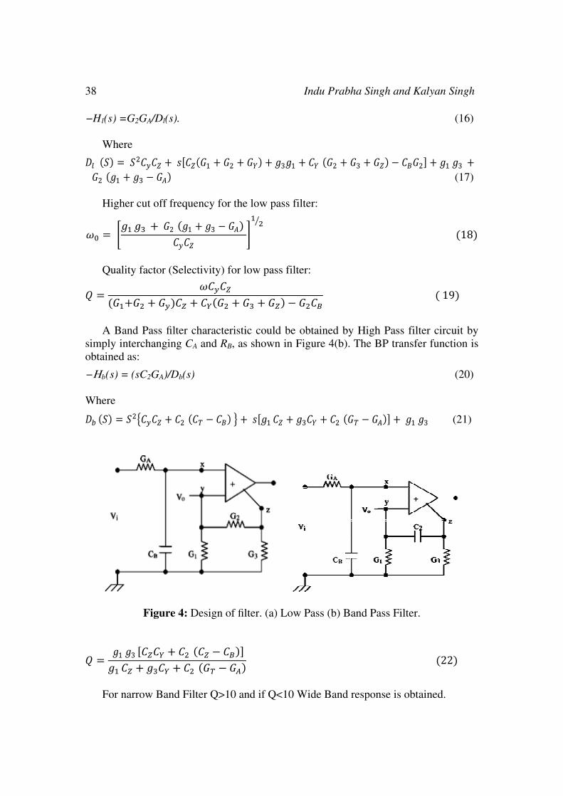
A Band Pass filter characteristic could be obtained by High Pass filter circuit by simply interchanging CA and RB, as shown in Figure 4(b). The BP transfer function is obtained as:
−Hb(s) = (sC2GA)/Db(s) (20) Where
(21)
Figure 4: Design of filter. (a) Low Pass (b) Band Pass Filter.
22
For narrow Band Filter Q>10 and if Q<10 Wide Band response is obtained.

A Review on Single CFA based Multifunctional Network 39
Simulation and Experimental Results All the functions of the multifunction network had experimentally been verified through hardware implementation and PSPICE macromodel simulation. The integrator/differentiator structures had been tested for time-domain response using square/triangular wave inputs, respectively. Good quality response on wave conversion up to 5 MHz was obtained, as shown in Figure 5.
(a) Integrator type I (b) Integrator type II
(c) Differentiator (d) Low Pass Filter
(e) High Pass Filter (f) Band Pass Filter.
Figure 5: Pspice simulation results of different Networks.
40 Indu Prabha Singh and Kalyan Singh
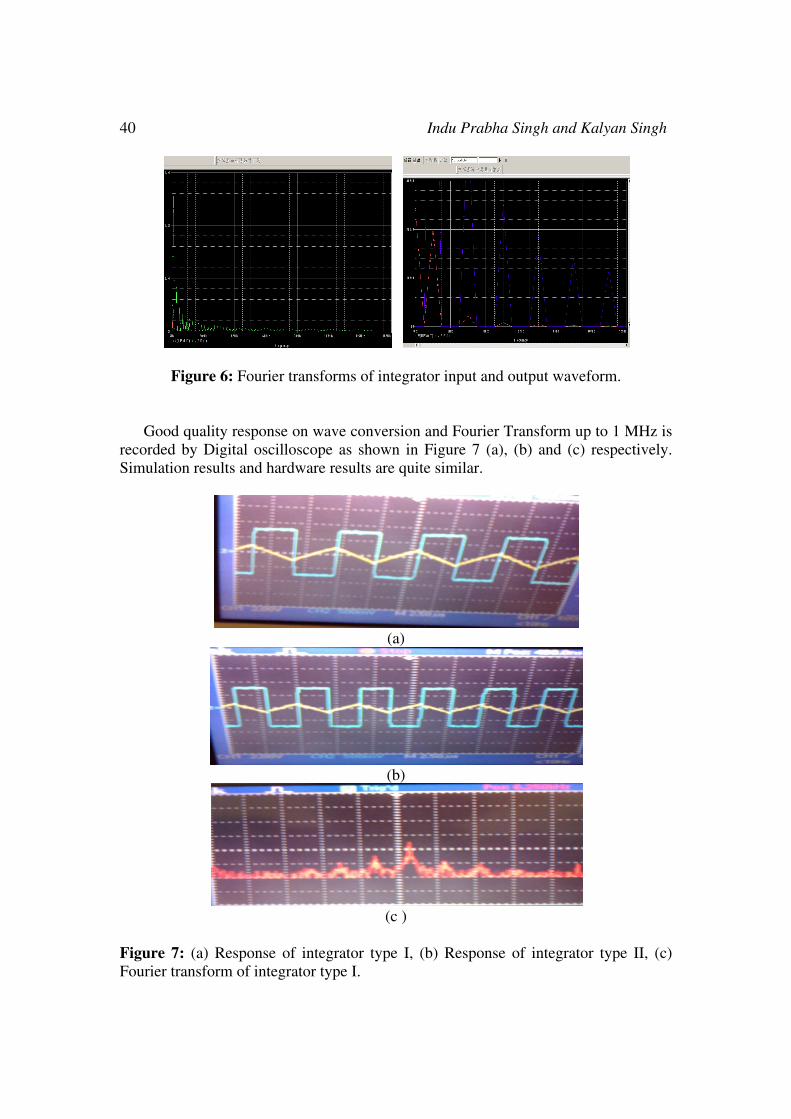
Figure 6: Fourier transforms of integrator input and output waveform. Good quality response on wave conversion and Fourier Transform up to 1 MHz is recorded by Digital oscilloscope as shown in Figure 7 (a), (b) and (c) respectively. Simulation results and hardware results are quite similar.
(a)
(b)
(c )
Figure 7: (a) Response of integrator type I, (b) Response of integrator type II, (c) Fourier transform of integrator type I.
A Review on Single CFA based Multifunctional Network 41
Conclusion Various signal processing networks like integrator, differentiator and filters, using single CFA topology are presented and reviewed. The advantages of using CFA over VFA in designing different networks are also presented. The characteristics of the integrator/differentiator realization and usable frequency range are examined and verified. The various filter transfer functions are analyzed, along with the expressions for the filter parameters ωo and Q. The simplified design equations for all the existing circuit functions are summarized. Some hardware realization results are also included. References
[1] B. Wilson, "Recent developments in current conveyor and current-mode circuits," Proceedings of IEEE, vol. 137, pp.63-77, 1990.
[2] G. W. Roberts and A. S. Sedra, "All current-mode frequency selective circuits," Electron. Lett., vol. 25, pp. 759-761,1989.
[3] C.M.Chang, "Currentmode allpass/notch and bandpass filter using single CCII," Electron. Lett., vol. 27, pp. 1812-1813, 1991.
[4] A. Sedra and K. C. Smith, “A second generation current conveyor and its applications,” IEEE Trans. Circ. Theory, vol. CT-17, pp. 132-134,Feb. 1970.
[5] J. W. Horng,1. R. Lay, C. W. Chang and M. H. Lee, "High input impedance voltage-mode multifunction filters using plus-type CClls," Electron Letts, vol. 33, pp. 472-473, 1997.
[6] J. W. Horng, "High-input impedance voltage-mode universal biquadratic filter using three plus-type CClls," IEEE Trans Circ Syst-II: Analog Digital Signal Process, vol. 48, pp. 996-997, 2001.
[7] J. W. Horng, "High-input impedance voltage-mode universal biquadratic filter using two OTAs and one CCII," IntJ Electron, vol. 90, pp. 185-191, 2003.
[8] J.W. Homg, "High input impedance voltage-mode universal biquadratic filters with three inputs using three plus-type CClls," Int J Electron, vol. 91, no. 8, pp. 465-475, 2004.
[9] E. Vidal, A. Poveda, and E. Alarcon, “Analysis and design of active R oscillators using the current feedback op-amp,” in Proc. ECS/IEEE ECCTD, Budapest, Hungary, ,pp.200–203, Aug. 1997.
[10] C. Tomazou and J. Lidgey, “Current feedback opamps: A blessing in disguise,” IEEE Circuits Devices Mag., vol. 10, no. 1, pp. 34–37,Jan. 1994.
[11] Linear Products Databack. Norwood, MA: Analog Devices, 1990. [12] G. Palumbo and S. Pennisi,“Current feedback amplifiers versus voltage
operational amplifiers,” IEEE Trans. Circuits Syst. I, Fundam. Theory Appl., vol. 48,no.5, pp.617–623,May 2001.
[13] R.K.Nagaria, Rakesh Kumar Singh and Subodh Wairya, “ On the new design of sinusoid voltage controlled oscillators using multiplier in CFA- based double integrator loop”, Journal of circuits, Systems and Computers (JCSC), vol.19, no.5, pp.939-948, August 2010.
42 Indu Prabha Singh and Kalyan Singh
[14] R.Senani, “Realization of a class of analog signal processing / signal generation circuits : Novel configurations using current feedback op-amps”, Frequenz, Journal of Telecommunication (Germany), vol.52 , pp.196-206, 1998.
[15] P. Venkateswaran, R.K. Nagaria, S.K. Sanyal and R. Nandi, “ Dual- input single- tunable integrators / differentiators using current feedback amplifier”, International Journal of Electronics (IJE), vol.90, no.2, pp.109-115, 2003.
[16] M. Higashimura, “Realisation of voltage-mode biquads using CCII+,” Electron. Lea, vol. 27, no. 15, pp. 1345-1346, July 1991.
[17] M. Higashimura and F. Fukui, “Realisation of biquadratic transfer functions using current conveyors,” Proc. Intemat. Symp. Circuits Syst.,(Singapore), June 1991, pp. 1424-1427.
[18] H. Tek and F. Anday, “Voltage transfer function synthesis using current conveyors,” Electron. Lett., vol. 25, no. 23, pp. 1552-1553, Nov. 1989.
[19] S.F.H. Naqshbandi and R. S. Sharma, “High input impedance current conveyor filters,” Znt. J. Electron., vol. 55, no. 3, pp. 499-500, 1983.
[20] J. L. Lee and S. I. Liu, “Integrator and differentiator with time constant multiplication using current feedback amplifier,” Electron. Lett., vol. 37,no.6, pp.331–333,Mar. 2001.
[21] R.K. Nagaria, P. Venkateswaran, S. K. Sanyal, and R. Nandi, “Newsimple integrators and diffentiators using current feedback amplifiers,”J. Frequenz, vol.57, pp.119–122, May/Jun. 2003.
[22] R.Nandi, S.K. Sanyal and T.K.Bandyopadhyay, “Single CFA- based integrator, differentiator, filter, and sinusoid oscillator,” IEEE Trans. on Instrumentation and Measurement, vol.58, no.8, pp. 2557- 2564, August 2009.