520.216 Introduction to VLSI Systems Lecture 3 …andreou/216/Archives/2012/Handouts/... · 520.216...
15
520.216 Introduction to VLSI Systems 1 520.216 Introduction to VLSI Systems Lecture 3 Integrated Circuits Fabrication and Very Large Scale Integration
Transcript of 520.216 Introduction to VLSI Systems Lecture 3 …andreou/216/Archives/2012/Handouts/... · 520.216...

520.216 Introduction to VLSI Systems 1
520.216Introduction to VLSI Systems
Lecture 3
Integrated Circuits Fabricationand
Very Large Scale Integration
520.216 Introduction to VLSI Systems 2
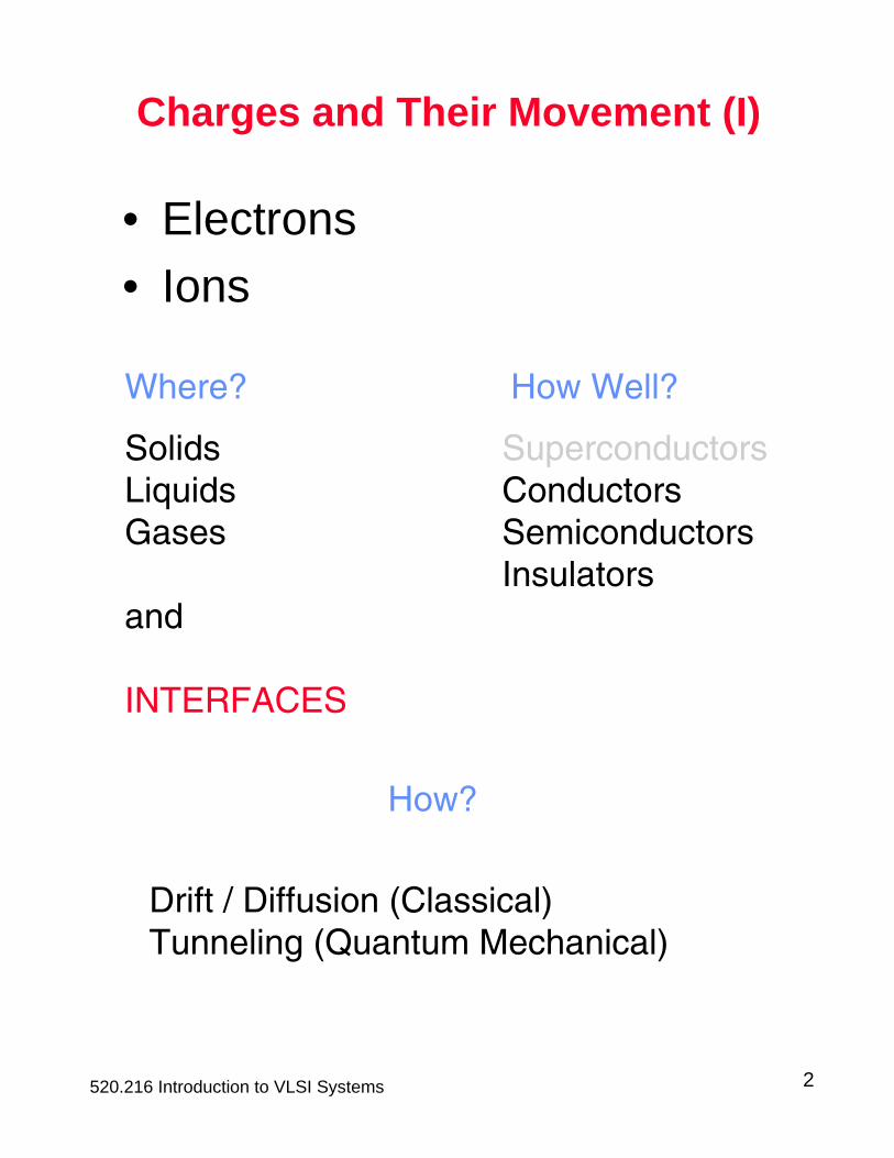
Charges and Their Movement (I)
• Electrons• Ions
SuperconductorsConductorsSemiconductorsInsulators
SolidsLiquidsGases
and
INTERFACES
Where? How Well?
How?
Drift / Diffusion (Classical)Tunneling (Quantum Mechanical)

520.216 Introduction to VLSI Systems 3
Charges and Their Movement (II)
FUNCTIONAL STRUCTURAL
• Electrical conduits(1D, 2D, 3D)• Transistors• Switches
• Etching• Film deposition(electroplating)
REDOX
We now consider transport in the solid-state and more specifically in the semiconductor Silicon
the microelectronics world does not use SI units! distance will be measured in cm and not meters.
for example: conductivity has units of ohm-cm

520.216 Introduction to VLSI Systems 4
Silicon!

520.216 Introduction to VLSI Systems 5
SiliconSisemiconductor
P.D. Neillist, "Incoherent Transmission Electron Microscopy" Phys. Rev. Lett. 81, 4156 ( 9 Nov. 1998)
Silicon molecule 5 silicon atoms in a unit cellDiamond latticeCovalent bonds
14 electrons4 valence electrons
Silicon molecules: http://www.eere.energy.gov/pv/simolecule.html
0.543 nm0.235 nm
Si Si Si
Si Si Si
Si Si Si
electronsholes
520.216 Introduction to VLSI Systems 6
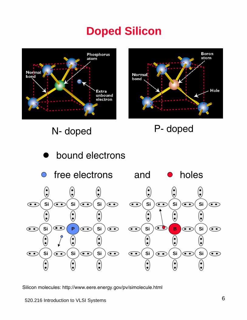
Doped Silicon
N- doped P- doped
Silicon molecules: http://www.eere.energy.gov/pv/simolecule.html
Si Si Si
Si P Si
Si Si Si
free electrons and holes
Si Si Si
Si B Si
Si Si Si
bound electrons

520.216 Introduction to VLSI Systems 7
Equilibrium Carrier Densities
2i
o D oD
nn N and p n typeN
= = −
2i
o A oA
np N and n p typeN
= = −
where no is electron and po hole carrier concentrations
in most cases of interest the donor doping ND or acceptor NA doping concentration is much larger than the intrinsic concentration ni so that
2 20 310 cmn o in p n −= =
by convention, donor or acceptor concentrations as well as electron and hole concentrations are given as a number per cm3

520.216 Introduction to VLSI Systems 8
Integrated Circuit Fabrication

520.216 Introduction to VLSI Systems 9
Where is it done?
UMC 300mm wafers

520.216 Introduction to VLSI Systems 10
Basic CMOS components
• Conductors• Switches (MOS transistors)• Capacitors (MOS capacitors)• Inductors• Resistors

520.216 Introduction to VLSI Systems 11
Bulk CMOS Technology (I)
p-substrate
n-well
n++p++
Polysilicon 1

520.216 Introduction to VLSI Systems 12
polysilicon 2
contact metal 1
Bulk CMOS Technology (II)

520.216 Introduction to VLSI Systems 13
vias metal 2
metal 3
Bulk CMOS Technology (III)

520.216 Introduction to VLSI Systems 14
CMOS Inverter

520.216 Introduction to VLSI Systems 15
Metallization Details
IBM PowerPC 500nm
UMC CMOS 90nm