2006.06.14.VLSI symposia 2006, A. Matsuzawa, Tokyo Tech. 1 Introduction to Embedded Data Converters...
74
2006.06.14. VLSI symposia 2006, A. Matsuzawa , Tokyo Tech. 1 Introduction to Embedded Data Converters Akira Matsuzawa Tokyo Institute of Technology
-
Upload
janel-daniels -
Category
Documents
-
view
219 -
download
0
Transcript of 2006.06.14.VLSI symposia 2006, A. Matsuzawa, Tokyo Tech. 1 Introduction to Embedded Data Converters...
2006.06.14. VLSI symposia 2006, A. Matsuzawa, Tokyo Tech.
1
Introduction to Embedded Data Converters
Akira Matsuzawa
Tokyo Institute of Technology
2006.06.14.
VLSI symposia 2006, A. Matsuzawa, Tokyo Tech. 2
Contents
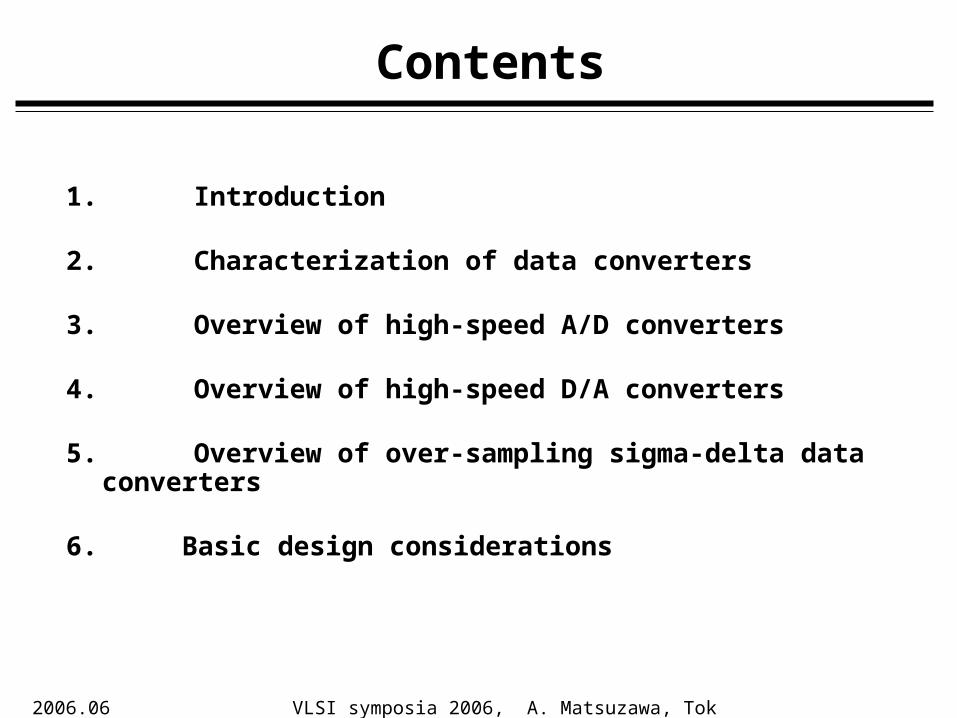
1. Introduction
2. Characterization of data converters
3. Overview of high-speed A/D converters
4. Overview of high-speed D/A converters
5. Overview of over-sampling sigma-delta data converters
6. Basic design considerations
2006.06.14.
VLSI symposia 2006, A. Matsuzawa, Tokyo Tech. 3
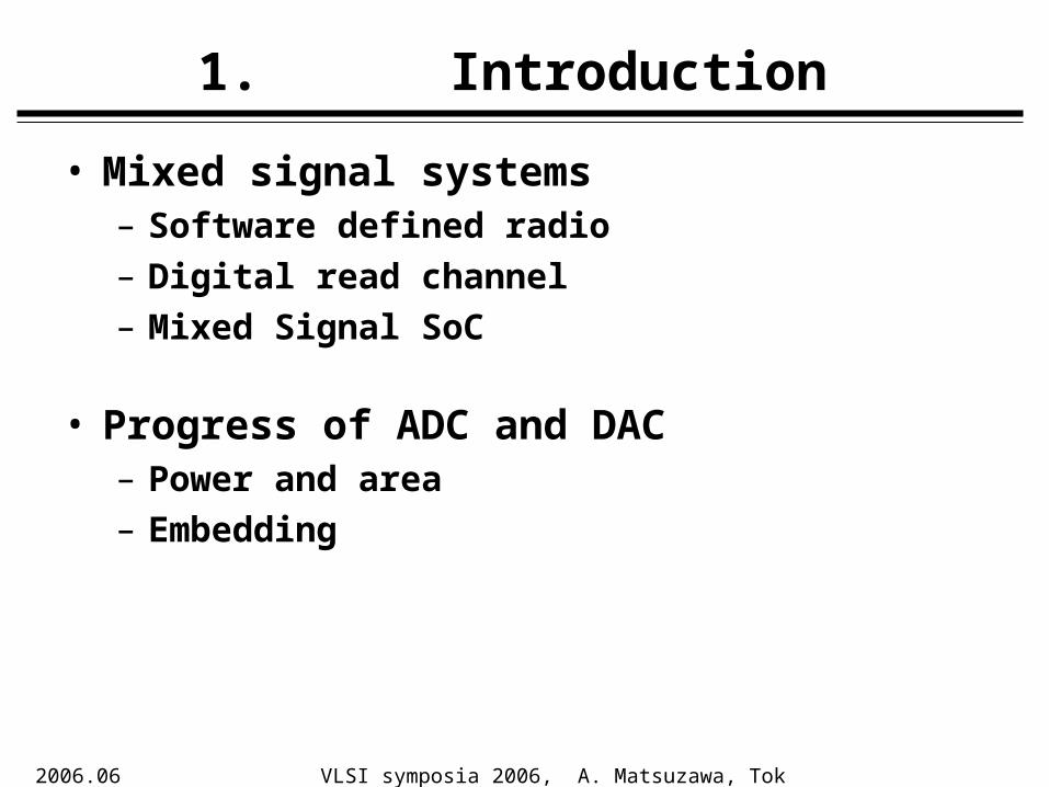
1. Introduction
• Mixed signal systems– Software defined radio– Digital read channel– Mixed Signal SoC
• Progress of ADC and DAC– Power and area– Embedding
2006.06.14.
VLSI symposia 2006, A. Matsuzawa, Tokyo Tech. 4
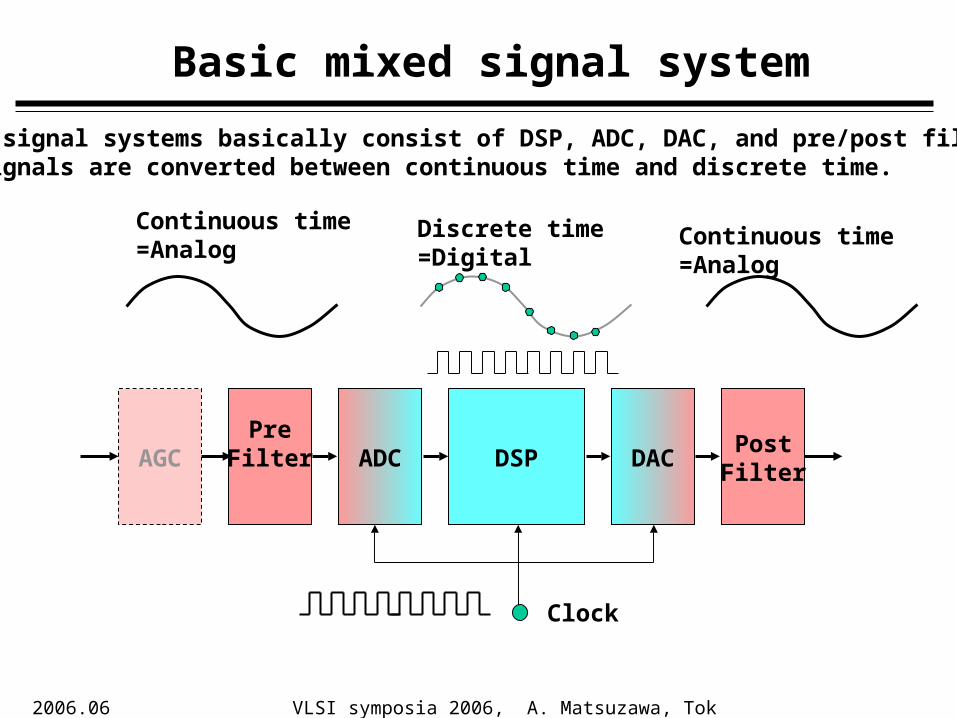
Basic mixed signal system
DSPADC DACPre
FilterPostFilter
AGC
Clock
Continuous time=Analog
Discrete time=Digital
Continuous time=Analog
Mixed signal systems basically consist of DSP, ADC, DAC, and pre/post filters. The signals are converted between continuous time and discrete time.
2006.06.14.
VLSI symposia 2006, A. Matsuzawa, Tokyo Tech. 5
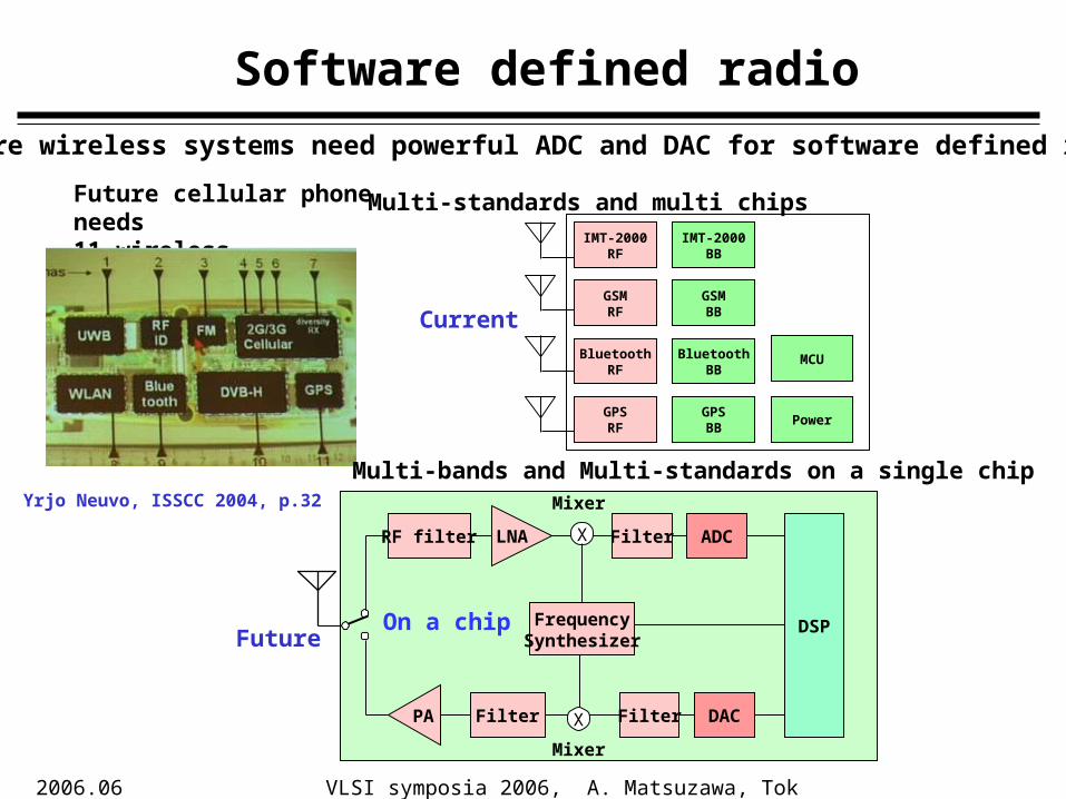
Software defined radio
IMT-2000RF
GSMRF
BluetoothRF
GPSRF
GPSBB
BluetoothBB
GSMBB
IMT-2000BB
MCU
Power
Multi-standards and multi chipsFuture cellular phone needs 11 wireless standards!!
Current
Yrjo Neuvo, ISSCC 2004, p.32
RF filter LNA X Filter ADC
FrequencySynthesizer
FilterPA DACX Filter
DSP
Mixer
Mixer
Future
Multi-bands and Multi-standards on a single chip
Future wireless systems need powerful ADC and DAC for software defined radio.
On a chip
2006.06.14.
VLSI symposia 2006, A. Matsuzawa, Tokyo Tech. 6
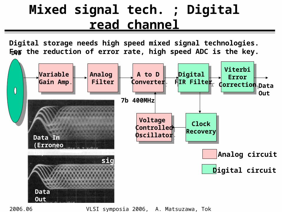
Mixed signal tech. ; Digital read channel
Variable Gain Amp.
Variable Gain Amp.
Analog Filter
Analog Filter
A to DConverter
A to DConverter
Digital FIR Filter
Digital FIR Filter
ViterbiError
Correction
ViterbiError
Correction
ClockRecovery
ClockRecovery
Voltage ControlledOscillator
Voltage ControlledOscillator
DataOut
Data In(Erroneous)
Data Out(No error)
Analog circuit
Digital circuit
Digital storage needs high speed mixed signal technologies.For the reduction of error rate, high speed ADC is the key.
Pickup signal
DVD
7b 400MHz
2006.06.14.
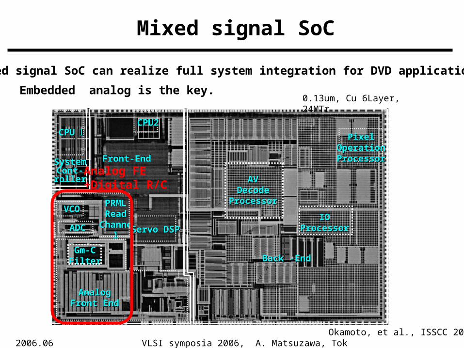
VLSI symposia 2006, A. Matsuzawa, Tokyo Tech. 7
Mixed signal SoC
PixelOperationProcessor
PixelOperationProcessor
IOProcessor
IOProcessor
AVDecode
Processor
AVDecode
Processor
Back -EndBack -End
SystemCont-roller
SystemCont-roller
CPU1CPU1CPU2CPU2
VCOVCO
ADCADC
Gm-CFilterGm-CFilter
PRMLRead
Channel
PRMLRead
ChannelServo DSPServo DSP
AnalogFront End
AnalogFront End
Front-EndFront-End
Analog FE+Digital R/C
0.13um, Cu 6Layer, 24MTr
Okamoto, et al., ISSCC 2003
Mixed signal SoC can realize full system integration for DVD application.
Embedded analog is the key.
2006.06.14.
VLSI symposia 2006, A. Matsuzawa, Tokyo Tech. 8
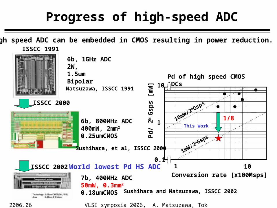
Progress of high-speed ADC
0.1
10
Pd
/ 2N
Gsp
s [m
W]
Pd of high speed CMOS ADCs
Conversion rate [x100Msps]
1
1mW/2N Gsps
10mW/2N Gsps
This Work
101
6b, 1GHz ADC2W,1.5um Bipolar
6b, 800MHz ADC400mW, 2mm2
0.25umCMOS
7b, 400MHz ADC50mW, 0.3mm2
0.18umCMOS
ISSCC 2002
ISSCC 2000
Matsuzawa, ISSCC 1991
World lowest Pd HS ADC
High speed ADC can be embedded in CMOS resulting in power reduction.ISSCC 1991
Sushihara and Matsuzawa, ISSCC 2002
Sushihara, et al, ISSCC 2000
1/8
2006.06.14.
VLSI symposia 2006, A. Matsuzawa, Tokyo Tech. 9
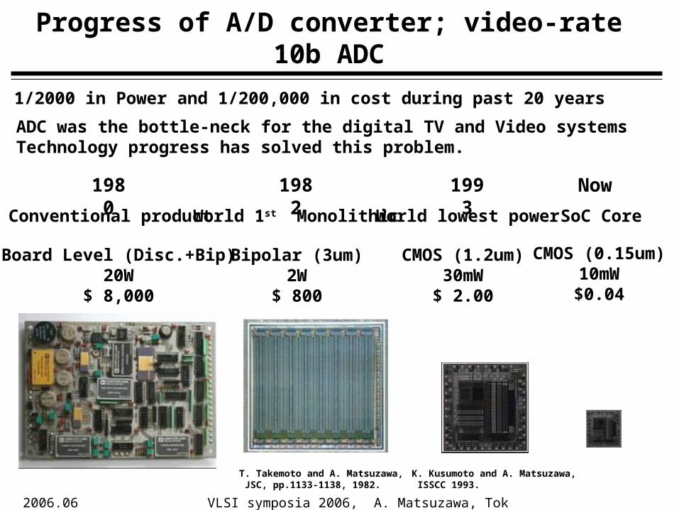
Progress of A/D converter; video-rate 10b ADC
1980 1982 1993 Now
Board Level (Disc.+Bip)20W
$ 8,000
Conventional product World 1st Monolithic
Bipolar (3um)2W
$ 800
World lowest power
CMOS (1.2um)30mW$ 2.00
CMOS (0.15um)10mW$0.04
SoC Core
1/2000 in Power and 1/200,000 in cost during past 20 years
ADC was the bottle-neck for the digital TV and Video systemsTechnology progress has solved this problem.
K. Kusumoto and A. Matsuzawa, ISSCC 1993.
T. Takemoto and A. Matsuzawa, JSC, pp.1133-1138, 1982.
2006.06.14.
VLSI symposia 2006, A. Matsuzawa, Tokyo Tech. 10
1
10
100
1000
10000
1980 1985 1990 1995 2000 2005 2010Year
Pow
er (
mW
)
2
5
20
50
200
500
2000
5000 FlashTwo-stepSubrangingFolding/InterpolatingPipeline
OthersLook-ahead Pipeline
1
10
100
1000
10000
1980 1985 1990 1995 2000 2005 2010Year
Pow
er (
mW
)
2
5
20
50
200
500
2000
5000 FlashTwo-stepSubrangingFolding/InterpolatingPipeline
OthersLook-ahead Pipeline
FlashTwo-stepSubrangingFolding/InterpolatingPipeline
OthersLook-ahead Pipeline
0.1
1.0
10.0
100.0
1980 1985 1990 1995 2000 2005 2010
Year
Are
a s
ize
(mm
2)
0.2
0.5
2.0
5.0
20.0
50.0FlashTwo-stepSubrangingFolding/InterpolatingPipeline
OthersLook-ahead Pipeline
0.1
1.0
10.0
100.0
1980 1985 1990 1995 2000 2005 2010
Year
Are
a s
ize
(mm
2)
0.2
0.5
2.0
5.0
20.0
50.0FlashTwo-stepSubrangingFolding/InterpolatingPipeline
OthersLook-ahead Pipeline
FlashTwo-stepSubrangingFolding/InterpolatingPipeline
OthersLook-ahead Pipeline
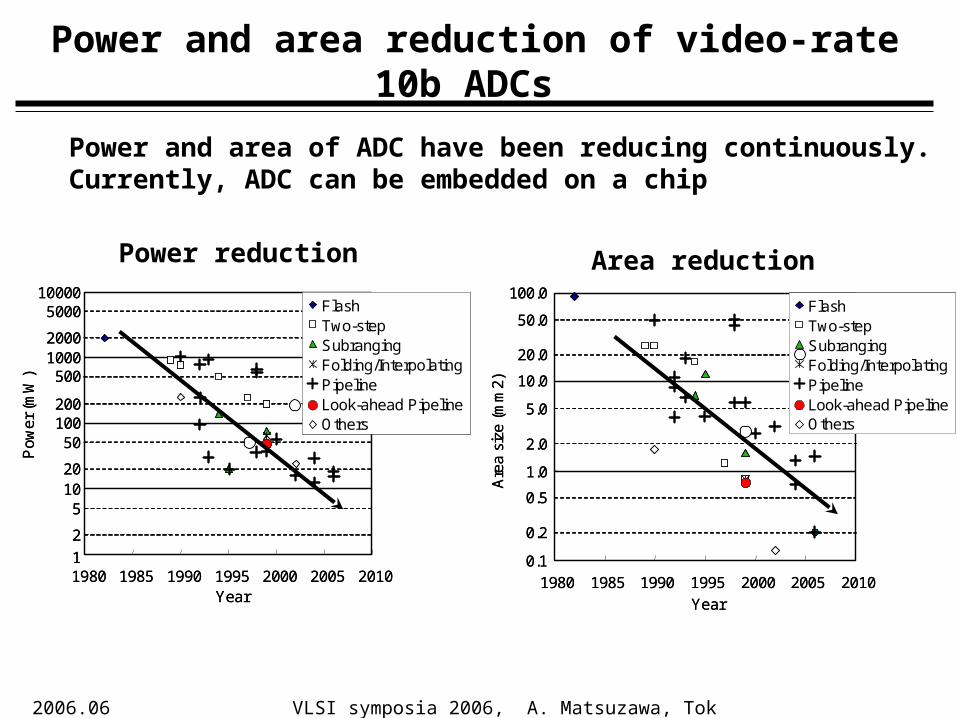
Power reduction Area reduction
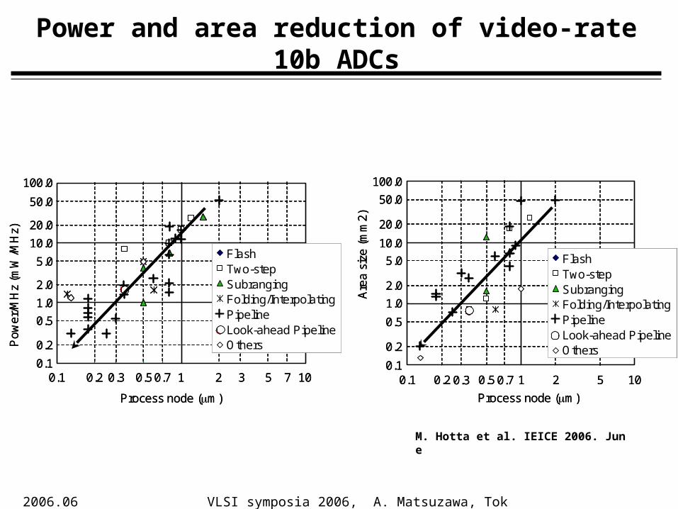
Power and area reduction of video-rate 10b ADCs
Power and area of ADC have been reducing continuously.Currently, ADC can be embedded on a chip
2006.06.14.
VLSI symposia 2006, A. Matsuzawa, Tokyo Tech. 11
0.1
1.0
10.0
100.0
0.1 1 10
Process node (m)
Po
we
r/M
Hz
(mW
/MH
z)
0.2 0.3 0.5 0.7 2 3 5 7
0.2
0.5
2.0
5.0
20.0
50.0
FlashTwo-stepSubrangingFolding/InterpolatingPipeline
OthersLook-ahead Pipeline
0.1
1.0
10.0
100.0
0.1 1 10
Process node (m)
Po
we
r/M
Hz
(mW
/MH
z)
0.2 0.3 0.5 0.7 2 3 5 7
0.2
0.5
2.0
5.0
20.0
50.0
FlashTwo-stepSubrangingFolding/InterpolatingPipeline
OthersLook-ahead Pipeline
FlashTwo-stepSubrangingFolding/InterpolatingPipeline
OthersLook-ahead Pipeline
0.1
1.0
10.0
100.0
0.1 1 10
Process node (m)
Are
a s
ize
(m
m2
)
0.2 0.5 2 5
0.2
0.5
2.0
5.0
20.0
50.0
FlashTwo-stepSubrangingFolding/InterpolatingPipeline
OthersLook-ahead Pipeline
0.3 0.70.1
1.0
10.0
100.0
0.1 1 10
Process node (m)
Are
a s
ize
(m
m2
)
0.2 0.5 2 5
0.2
0.5
2.0
5.0
20.0
50.0
FlashTwo-stepSubrangingFolding/InterpolatingPipeline
OthersLook-ahead Pipeline
FlashTwo-stepSubrangingFolding/InterpolatingPipeline
OthersLook-ahead Pipeline
0.3 0.7
M. Hotta et al. IEICE 2006. June
Power and area reduction of video-rate 10b ADCs
2006.06.14.
VLSI symposia 2006, A. Matsuzawa, Tokyo Tech. 12
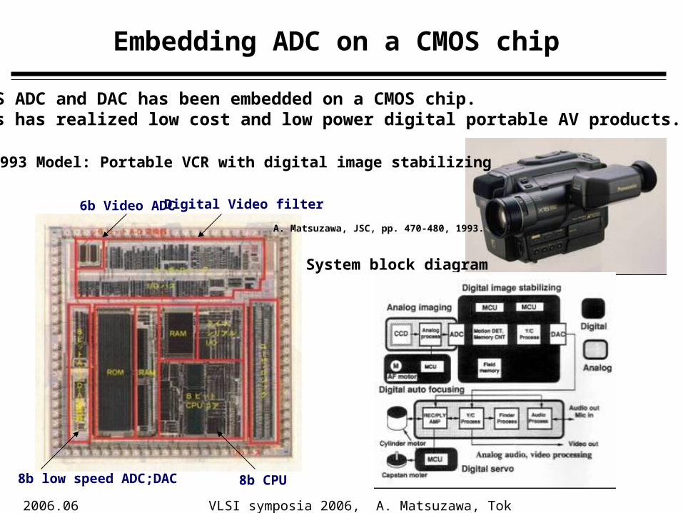
Embedding ADC on a CMOS chip
6b Video ADC
8b low speed ADC;DAC
Digital Video filter
8b CPU
1993 Model: Portable VCR with digital image stabilizing
CMOS ADC and DAC has been embedded on a CMOS chip.This has realized low cost and low power digital portable AV products.
System block diagram
A. Matsuzawa, JSC, pp. 470-480, 1993.
2006.06.14.
VLSI symposia 2006, A. Matsuzawa, Tokyo Tech. 13
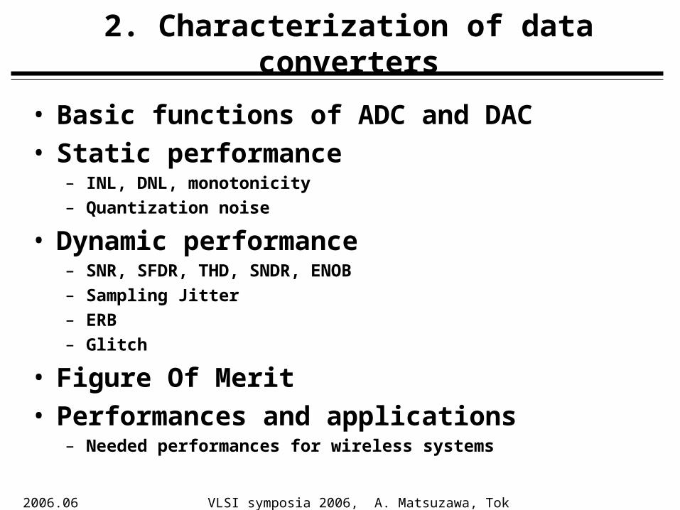
2. Characterization of data converters
• Basic functions of ADC and DAC• Static performance
– INL, DNL, monotonicity
– Quantization noise
• Dynamic performance– SNR, SFDR, THD, SNDR, ENOB
– Sampling Jitter
– ERB
– Glitch
• Figure Of Merit• Performances and applications
– Needed performances for wireless systems
2006.06.14.
VLSI symposia 2006, A. Matsuzawa, Tokyo Tech. 14
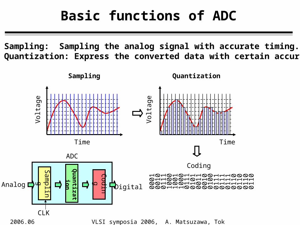
Basic functions of ADC
Time
Vol
tage
Time
Sampling Quantization
0001
0010
0111
1000
1001
1000
0111
0101
0011
0010
0100
0111
0111
0111
0110
0110
0110
0110
Coding
Digital
Sam
pling
Qu
antization
Coding
Analog
ADC
Sampling: Sampling the analog signal with accurate timing.Quantization: Express the converted data with certain accuracy.
CLK
Vol
tage
2006.06.14.
VLSI symposia 2006, A. Matsuzawa, Tokyo Tech. 15
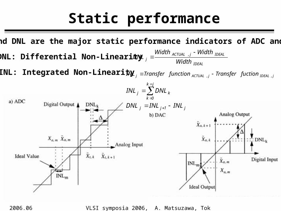
Static performance
INL: Integrated Non-Linearity
INL and DNL are the major static performance indicators of ADC and DAC.
DNL: Differential Non-LinearityIDEAL
IDEALj,ACTUALj Width
WidthWidthDNL
j,IDEALj,ACTUALj fuctionTransferfunctionTransferINL
j1jj
jk
0kkj
INLINLDNL
DNLINL
2006.06.14.
VLSI symposia 2006, A. Matsuzawa, Tokyo Tech. 16
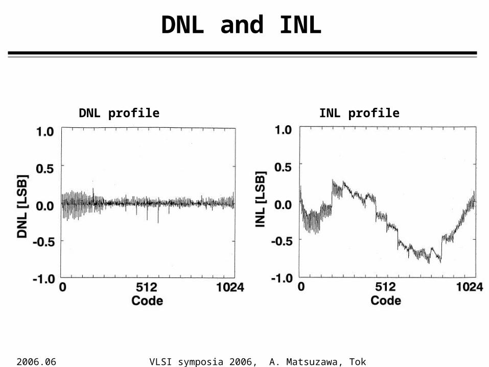
DNL and INL
DNL profile INL profile
2006.06.14.
VLSI symposia 2006, A. Matsuzawa, Tokyo Tech. 17
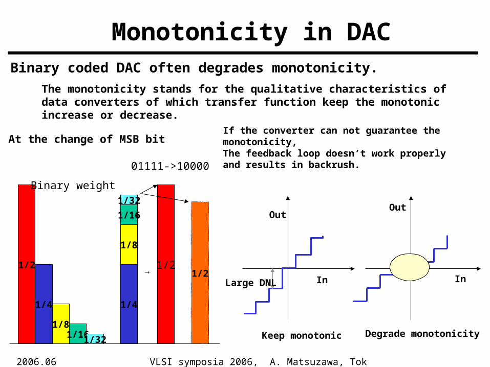
Monotonicity in DAC
Keep monotonic
In
Out
Large DNL
Degrade monotonicity
In
Out
1/2
1/4
1/81/161/32
1/2
1/4
1/8
1/16
1/32
01111->10000
→ 1/2
Binary weight
At the change of MSB bit
Binary coded DAC often degrades monotonicity.
The monotonicity stands for the qualitative characteristics of data converters of which transfer function keep the monotonic increase or decrease.
If the converter can not guarantee the monotonicity, The feedback loop doesn’t work properly and results in backrush.
2006.06.14.
VLSI symposia 2006, A. Matsuzawa, Tokyo Tech. 18
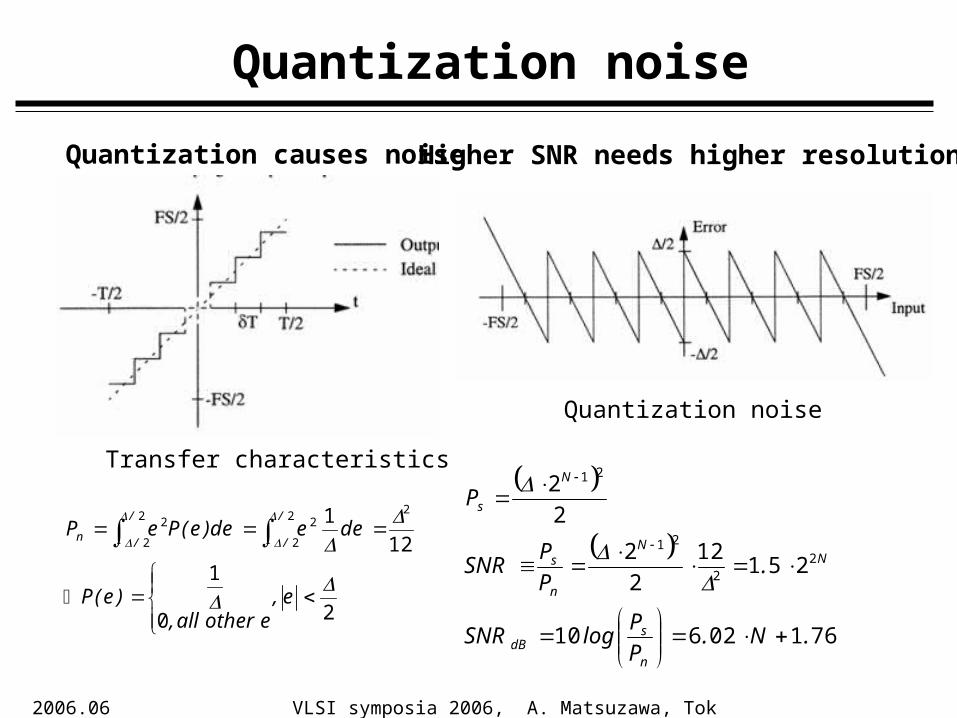
Quantization noise
Transfer characteristics
Quantization noise
20
112
1 22
2
22
2
2
e,eotherall,
)e(P
deede)e(PeP/
/
/
/n
76102610
25112
22
22
22
21
21
.N.PP
logSNR
.PP
SNR
P
n
sdB
NN
n
s
N
s
Quantization causes noise Higher SNR needs higher resolution
2006.06.14.
VLSI symposia 2006, A. Matsuzawa, Tokyo Tech. 19
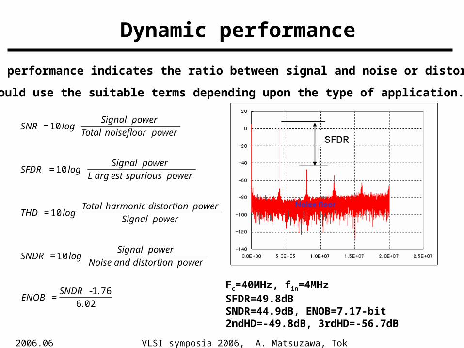
Dynamic performance
026761
10
10
10
10
..SNDR
ENOB
powerdistortionandNoisepowerSignal
logSNDR
powerSignalpowerdistortionharmonicTotal
logTHD
powerspuriousestargLpowerSignal
logSFDR
powernoisefloorTotalpowerSignal
logSNR
-=
=
=
=
=
Dynamic performance indicates the ratio between signal and noise or distortion.
We should use the suitable terms depending upon the type of application.
Fc=40MHz, fin=4MHzSFDR=49.8dBSNDR=44.9dB, ENOB=7.17-bit2ndHD=-49.8dB, 3rdHD=-56.7dB
2006.06.14.
VLSI symposia 2006, A. Matsuzawa, Tokyo Tech. 20
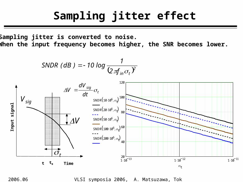
Sampling jitter effect
2tinf2
1log10)dB(SNDR
Sampling jitter is converted to noise.When the input frequency becomes higher, the SNR becomes lower.
110 13 110 12 110 1120
40
60
80
100
120
SNDR 10 106 t SNDR 20 106 t SNDR 50 106 t SNDR 100 106 t SNDR 200 106 t
tTime
Inp
ut
sig
na
l
t0t
V
t
tsig
dt
dVV
sigV
2006.06.14.
VLSI symposia 2006, A. Matsuzawa, Tokyo Tech. 21
EN
OB
(b
it)
Input frequency (MHz)
3002001003
4
5
6
SNR
SNDR
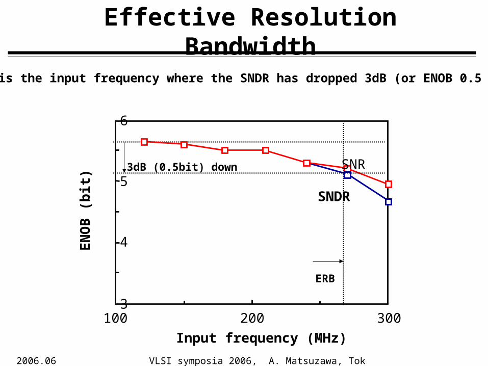
Effective Resolution Bandwidth
3dB (0.5bit) down
ERB
ERB is the input frequency where the SNDR has dropped 3dB (or ENOB 0.5 bit)
2006.06.14.
VLSI symposia 2006, A. Matsuzawa, Tokyo Tech. 22
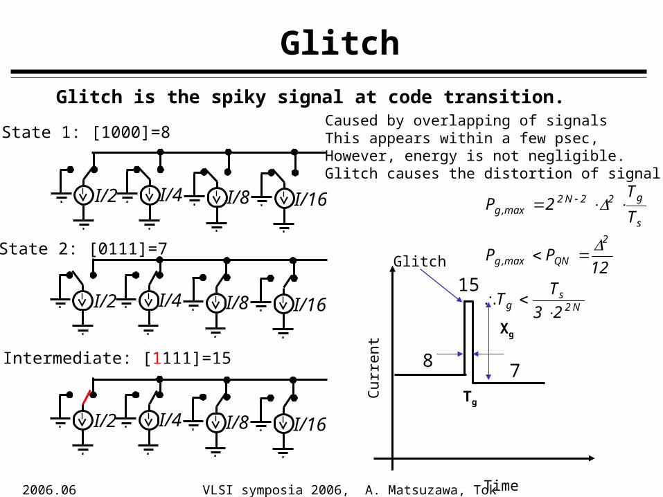
Glitch
I/2 I/4 I/8 I/16
I/2 I/4 I/8 I/16
I/2 I/4 I/8 I/16
State 1: [1000]=8
State 2: [0111]=7
Intermediate: [1111]=15 8
15
7C
urre
nt
Time
Glitch
Glitch is the spiky signal at code transition.Caused by overlapping of signalsThis appears within a few psec,However, energy is not negligible.Glitch causes the distortion of signal
Tg
Xg
N2s
g
2
QNmax,g
s
g22N2max,g
23
TT
12PP
T
T2P
2006.06.14.
VLSI symposia 2006, A. Matsuzawa, Tokyo Tech. 23
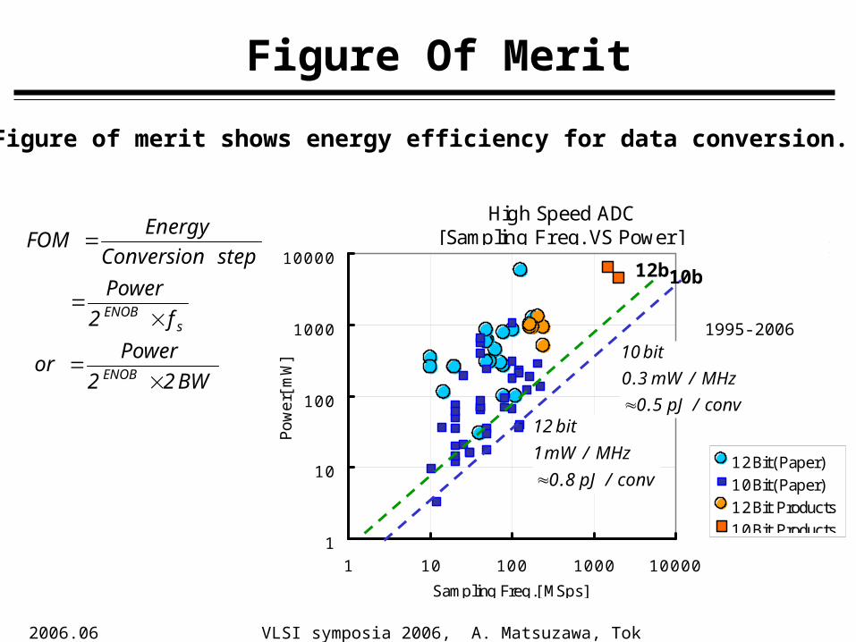
Figure Of Merit
BW22Power
or
f2Power
stepConversionEnergy
FOM
ENOB
sENOB
High Speed ADC
[Sampling Freq. VS Power]
1
10
100
1000
10000
1 10 100 1000 10000
Sampling Freq.[MSps]
Power[
mW]
12Bit(Paper)10Bit(Paper)12Bit Products10Bit Products.
J SSC,ISSCC,VLSI,CICC,ESSCC & Products(≧10Bit,≧10MSps)1995-2006
conv/pJ5.0
MHz/mW3.0
bit10
conv/pJ8.0
MHz/mW1
bit12
10b12b
Figure of merit shows energy efficiency for data conversion.
2006.06.14.
VLSI symposia 2006, A. Matsuzawa, Tokyo Tech. 24
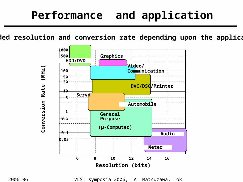
Performance and application
6 8 10 12 14 16
Resolution (bits)
Co
nve
rsio
n R
ate
(MH
z)
0.1
1
10
100
1000
5
3050
300500
0.5
0.05
HDD/DVDGraphics
Audio
GeneralPurpose
DVC/DSC/Printer
Video/Communication
Servo
(µ-Computer)
Automobile
Meter
Needed resolution and conversion rate depending upon the application.
2006.06.14.
VLSI symposia 2006, A. Matsuzawa, Tokyo Tech. 25
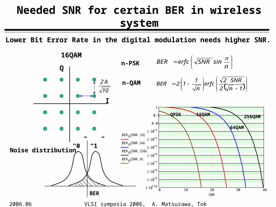
Needed SNR for certain BER in wireless system
Q
I
16QAM
10
A2
“1”“0”
BER
Noise distribution
1n2
SNR2erfc
n
112BER
Lower Bit Error Rate in the digital modulation needs higher SNR.
nsinSNRerfcBER
n-PSK
n-QAM
0 10 20 30 40110 10
110 9
110 8
110 7
110 6
110 5
110 4
110 3
0.01
0.1
1
BERq SNR 16( )
BERq SNR 64( )
BERq SNR 256( )
BERp SNR 4( )
SNR
16QAM
64QAM
256QAMQPSK
2006.06.14.
VLSI symposia 2006, A. Matsuzawa, Tokyo Tech. 26
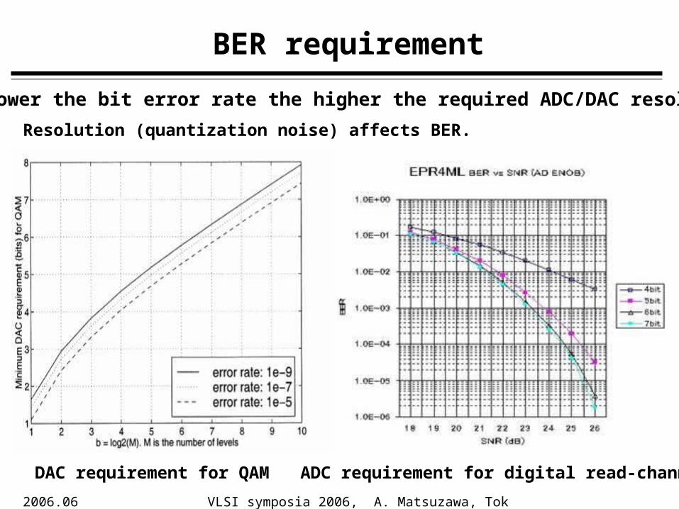
BER requirement
DAC requirement for QAM ADC requirement for digital read-channel
The lower the bit error rate the higher the required ADC/DAC resolution.
Resolution (quantization noise) affects BER.
2006.06.14.
VLSI symposia 2006, A. Matsuzawa, Tokyo Tech. 27
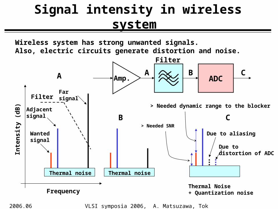
Signal intensity in wireless system
Amp. ADC
Filter
A B C
Thermal noise Thermal noise
Thermal Noise+ Quantization noise
Wantedsignal
Adjacentsignal
FarsignalFilter
Frequency
Inte
nsi
ty (
dB
)
A
B C
Due to aliasing
Due to distortion of ADC
> Needed SNR
> Needed dynamic range to the blocker
Wireless system has strong unwanted signals. Also, electric circuits generate distortion and noise.
2006.06.14.
VLSI symposia 2006, A. Matsuzawa, Tokyo Tech. 28
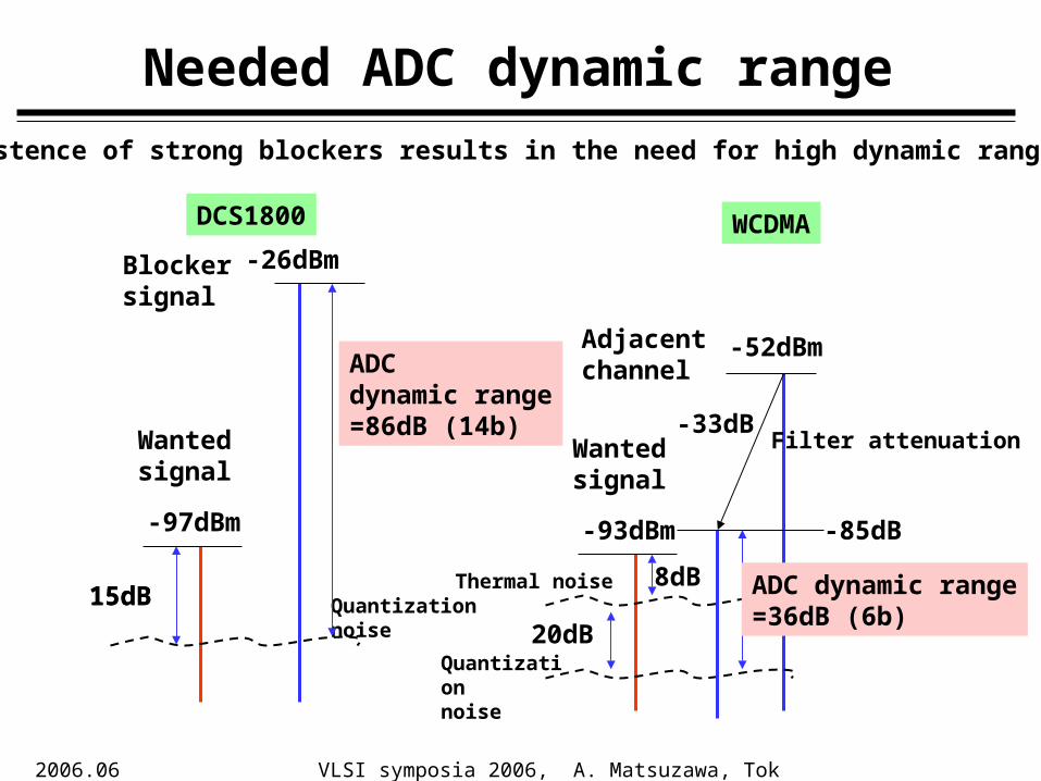
Needed ADC dynamic range
-26dBm
-97dBm
Quantizationnoise
Wantedsignal
Blockersignal
15dB15dB
ADC dynamic range=86dB (14b)
DCS1800
-52dBm
-93dBm
Quantizationnoise
Wantedsignal
Adjacentchannel
8dB
WCDMA
-33dB
-85dB
Filter attenuation
Thermal noise
20dB
Existence of strong blockers results in the need for high dynamic range ADC.
ADC dynamic range=36dB (6b)
2006.06.14.
VLSI symposia 2006, A. Matsuzawa, Tokyo Tech. 29
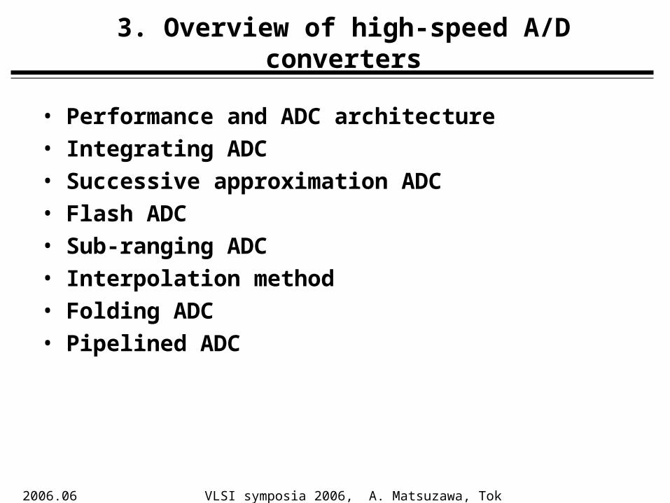
3. Overview of high-speed A/D converters
• Performance and ADC architecture• Integrating ADC• Successive approximation ADC• Flash ADC• Sub-ranging ADC• Interpolation method• Folding ADC• Pipelined ADC
2006.06.14.
VLSI symposia 2006, A. Matsuzawa, Tokyo Tech. 30
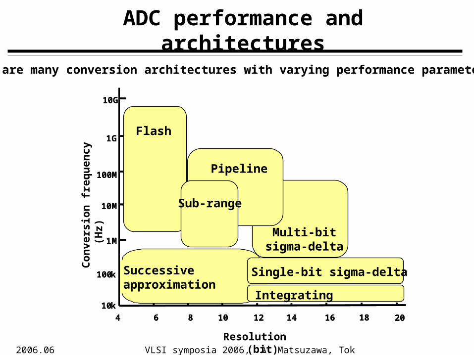
ADC performance and architectures
4 6 8 10 12 14 16
10M
1M
100k
10k
100M
1G
10G
20184 6 8 10 12 14 16
10M
1M
100k
10k
100M
1G
10G
2018
Co
nve
rsio
n f
req
uen
cy (
Hz)
Resolution (bit)
Successiveapproximation
Integrating
Flash
Sub-range
Multi-bitsigma-delta
Pipeline
Single-bit sigma-delta
There are many conversion architectures with varying performance parameters.
2006.06.14.
VLSI symposia 2006, A. Matsuzawa, Tokyo Tech. 31
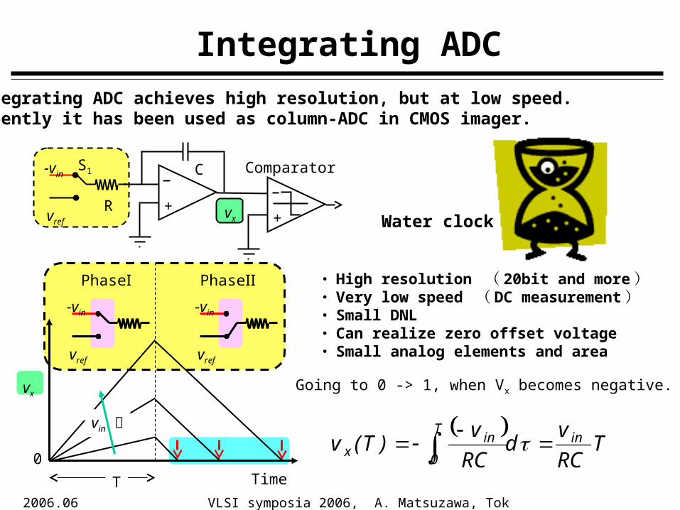
Integrating ADC
+ vx +
S1
vref
-vin Comparator
T Time
vx
R
C
vref
-vin
vref
-vin
0
vin 大
Going to 0 -> 1, when Vx becomes negative.
PhaseⅠ PhaseⅡ
T
RCv
dRCv
)T(v inT
0
inx
・ High resolution ( 20bit and more)・ Very low speed ( DC measurement)・ Small DNL・ Can realize zero offset voltage・ Small analog elements and area
Water clock
Integrating ADC achieves high resolution, but at low speed.Recently it has been used as column-ADC in CMOS imager.
2006.06.14.
VLSI symposia 2006, A. Matsuzawa, Tokyo Tech. 32
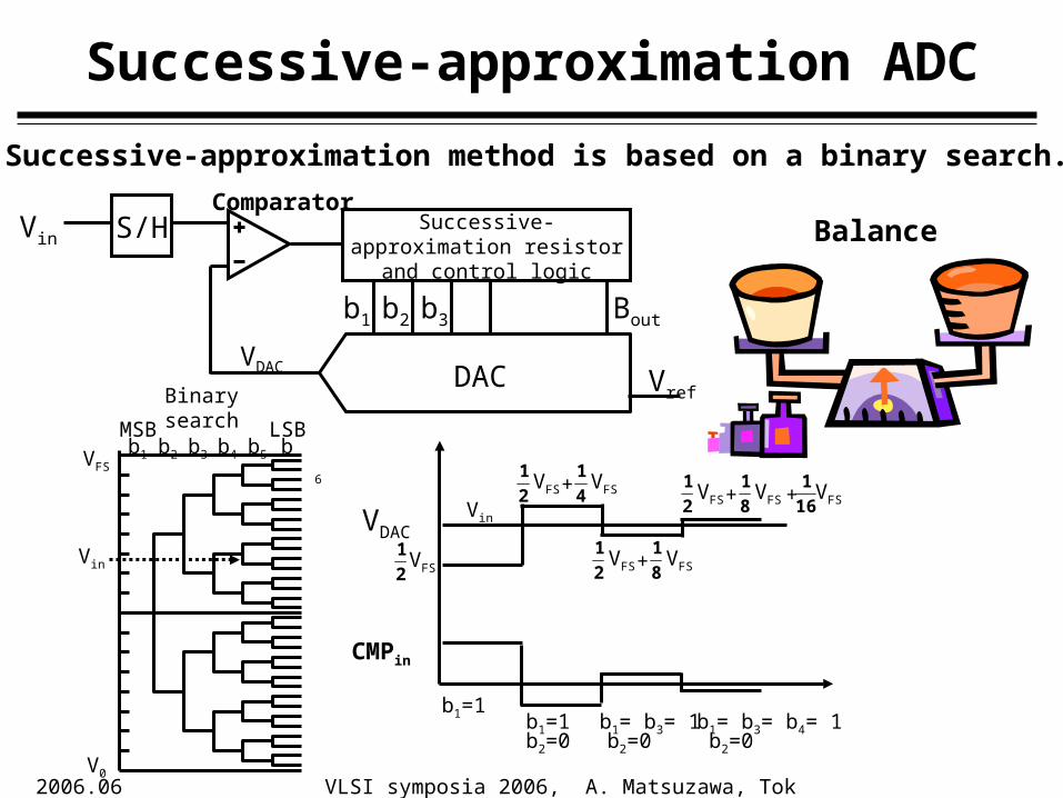
Successive-approximation ADC
b1 b2 b3 b4 b5 b
6
MSB LSB
VFS
V0
Binary search
Vin
VDACVin
VFS2
1
VFS2
1 VFS4
1+
VFS2
1 VFS8
1+
VFS2
1 VFS8
1+ VFS16
1+
b1=1b1=1b2=0
b1= b3= 1b2=0
b1= b3= b4= 1b2=0
S/HVin Successive-approximation resistor and control logic
b1 b2 b3 Bout
DAC Vref
VDAC
Comparator
CMPin
Balance
Successive-approximation method is based on a binary search.
2006.06.14.
VLSI symposia 2006, A. Matsuzawa, Tokyo Tech. 33
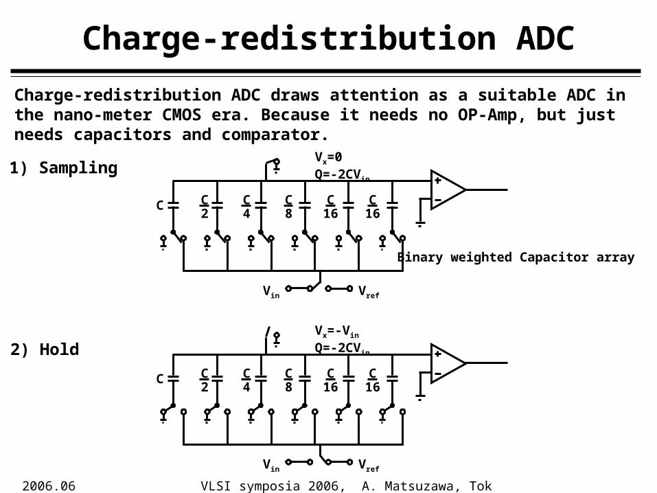
Charge-redistribution ADC
C C2
C4
C8
C16
C16
Vin Vref
Vx=0Q=-2CVin
1) Sampling
C C2
C4
C8
C16
C16
Vin Vref
Vx=-Vin
Q=-2CVin2) Hold
Binary weighted Capacitor array
Charge-redistribution ADC draws attention as a suitable ADC in the nano-meter CMOS era. Because it needs no OP-Amp, but just needs capacitors and comparator.
2006.06.14.
VLSI symposia 2006, A. Matsuzawa, Tokyo Tech. 34
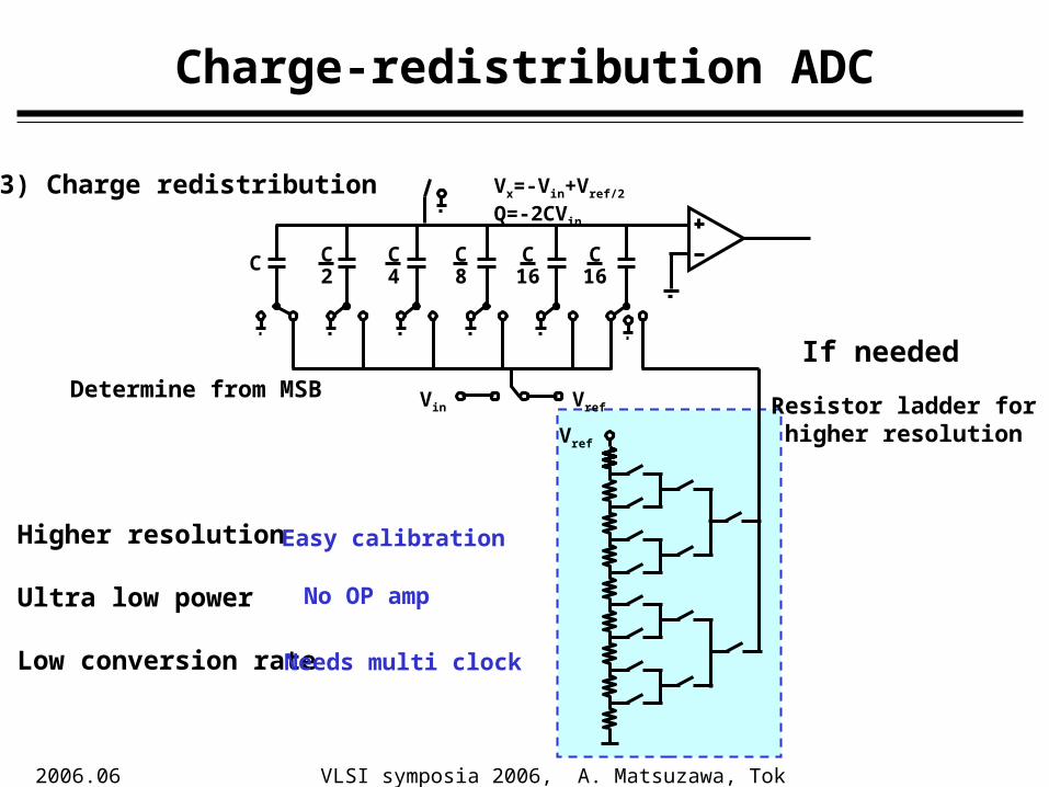
C C2
C4
C8
C16
C16
Vin Vref
Vx=-Vin+Vref/2 Q=-2CVin
Charge-redistribution ADC
Vref
Resistor ladder for higher resolution
Higher resolution
Ultra low power
Low conversion rate
3) Charge redistribution
Determine from MSB
If needed
Easy calibration
No OP amp
Needs multi clock
2006.06.14.
VLSI symposia 2006, A. Matsuzawa, Tokyo Tech. 35
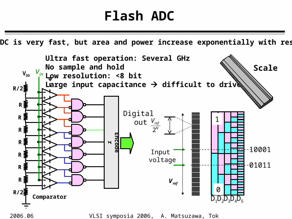
Flash ADC
R
R
R
R
R
R
R
VDD
+
+
+
+
+
+
+
+
R/2
R/2
vin
En
cod
er
Comparator
Φ
Digital out
Ultra fast operation: Several GHzNo sample and holdLow resolution: <8 bitLarge input capacitance difficult to drive
Flash ADC is very fast, but area and power increase exponentially with resolution.
10001
01011
D1D2D3D4D5
0
1
Input voltage
NrefV
2
refV
Scale
2006.06.14.
VLSI symposia 2006, A. Matsuzawa, Tokyo Tech. 36
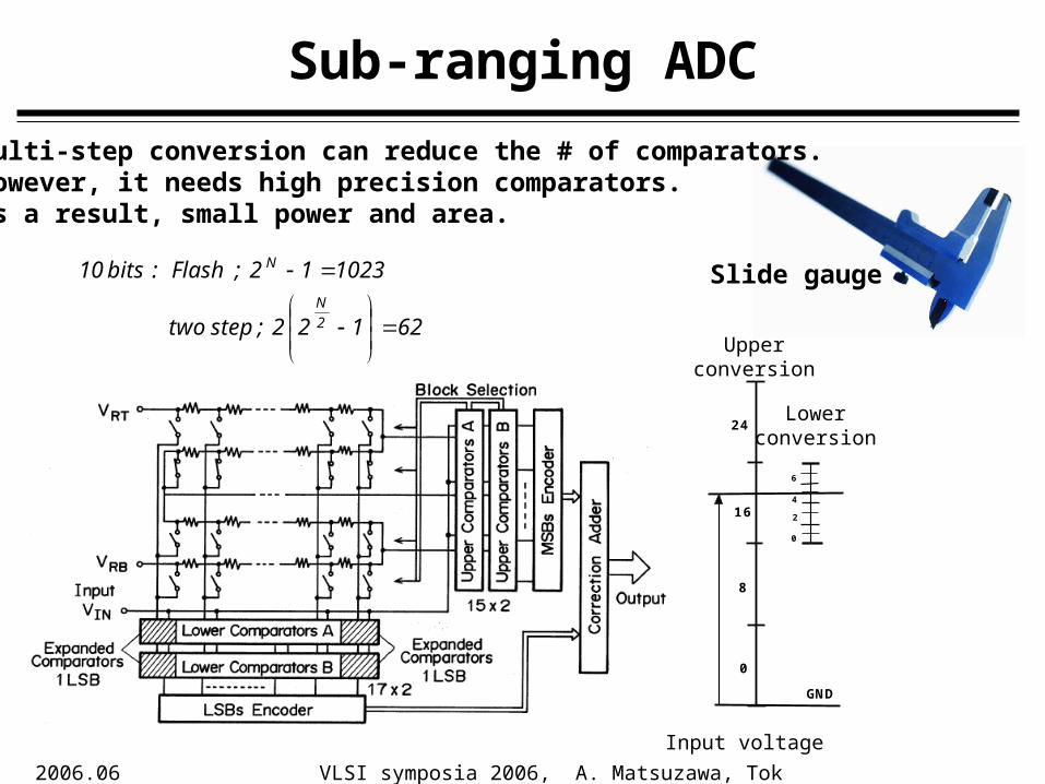
Sub-ranging ADC
GND
0
8
16
24
0
2
4
6
Input voltage
Upperconversion
Lowerconversion
Multi-step conversion can reduce the # of comparators.However, it needs high precision comparators.As a result, small power and area.
62122;steptwo
102312;Flash:bits10
2N
N
Slide gauge
2006.06.14.
VLSI symposia 2006, A. Matsuzawa, Tokyo Tech. 37
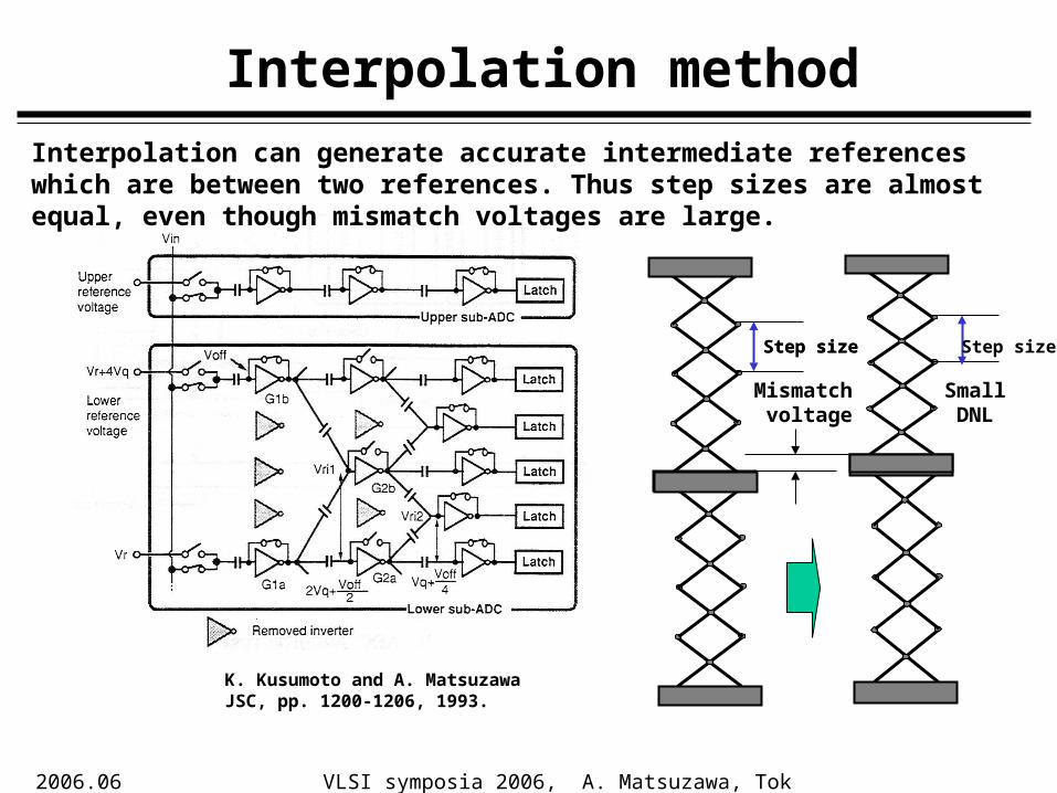
Interpolation method
Interpolation can generate accurate intermediate references which are between two references. Thus step sizes are almost equal, even though mismatch voltages are large.
Mismatch voltage
Small DNL
K. Kusumoto and A. MatsuzawaJSC, pp. 1200-1206, 1993.
Step sizeStep size Step size
2006.06.14.
VLSI symposia 2006, A. Matsuzawa, Tokyo Tech. 38
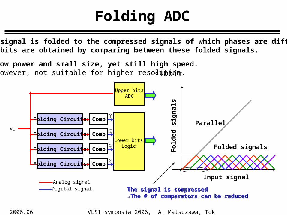
Folding ADC
Upper bitsADC
Lower bitsLogic
Comp
Comp
Comp
Comp
Folding Circuits
Folding Circuits
Folding Circuits
Folding Circuits
vin
Analog signal
Digital signal
①
②
③
④
Input signalF
old
ed s
ign
als
Parallel
Folded signals
The signal is compressedThe signal is compressed→→The # of comparators can be reducedThe # of comparators can be reduced
Input signal is folded to the compressed signals of which phases are different.Lower bits are obtained by comparing between these folded signals.
Low power and small size, yet still high speed.However, not suitable for higher resolution. <10bit
2006.06.14.
VLSI symposia 2006, A. Matsuzawa, Tokyo Tech. 39
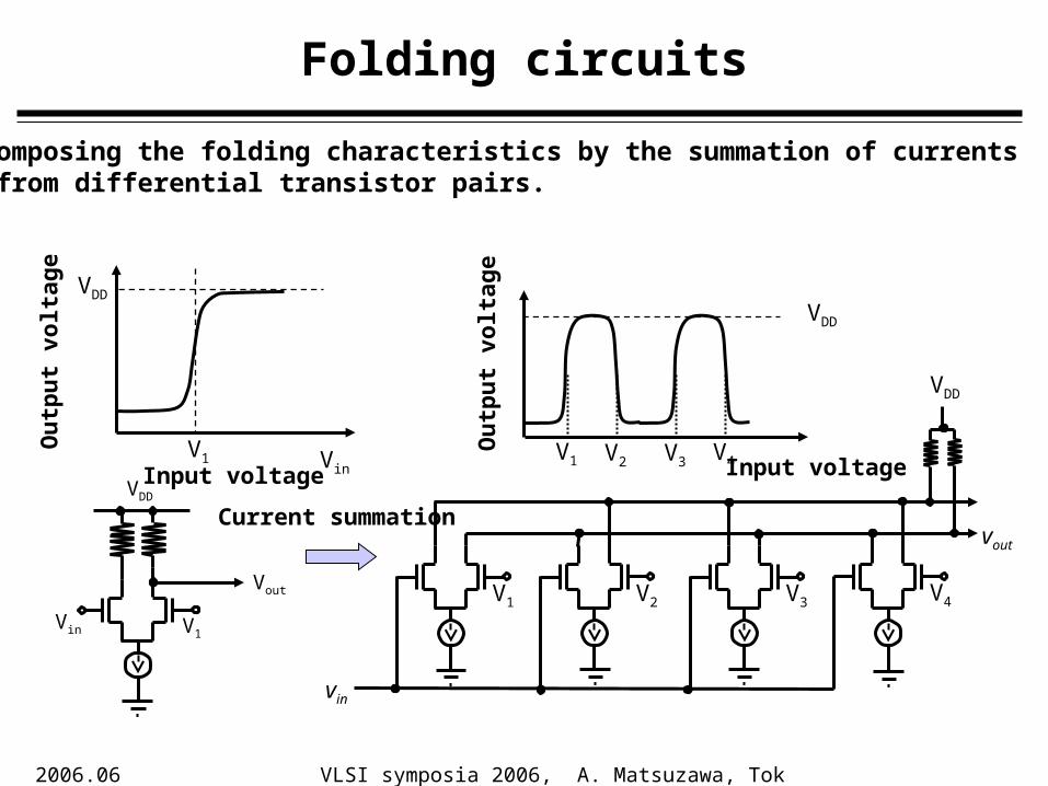
Folding circuits
VDD
vin
V1 V2 V3 V4
V1 V2 V3 V4 Input voltageO
utp
ut
volt
age
vout
VDD
Current summation
V1Vin
VDD
Vout
V1 VinInput voltage
Ou
tpu
t vo
ltag
e VDD
Composing the folding characteristics by the summation of currents from differential transistor pairs.
2006.06.14.
VLSI symposia 2006, A. Matsuzawa, Tokyo Tech. 40
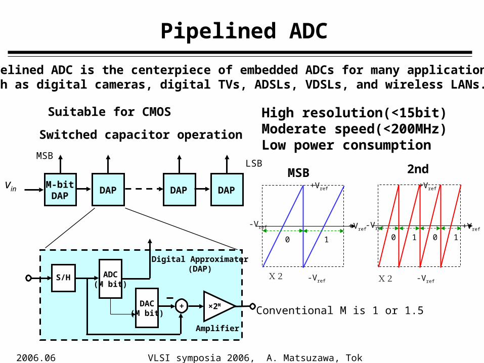
Pipelined ADC
vin M-bitDAP
DAP DAP DAP
MSBLSB
+ ×2M
Amplifier
S/H
Digital Approximater(DAP)
ADC(M bit)
DAC(M bit) Conventional M is 1 or 1.5
High resolution(<15bit)Moderate speed(<200MHz)Low power consumption
Suitable for CMOS
Switched capacitor operation
-Vref
+Vref
-Vref
+Vref
0 1
X2
-Vref
+Vref
-Vref
+Vref
0 1 0 1
X2
MSB 2nd
Pipelined ADC is the centerpiece of embedded ADCs for many applications,such as digital cameras, digital TVs, ADSLs, VDSLs, and wireless LANs.
2006.06.14.
VLSI symposia 2006, A. Matsuzawa, Tokyo Tech. 41
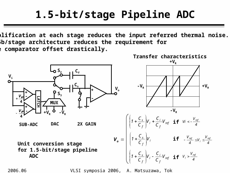
MUX
+VR -VR
LA
TC
H
4RV
4RV
SUB-ADC DAC 2X GAIN
Vi
Vo
Cf
Cs
S2
S3
+
-+-
-+
1.5-bit/stage Pipeline ADC
+VR-VR
+VR
-VR
reff
ii
f
s VCC
VCC
1
if
s VCC
1
reff
ii
f
s VCC
VCC
1
4
VVi refif
if4
VV
4
V refi
ref
if 4
VV ref
i
oVUnit conversion stage for 1.5-bit/stage pipeline ADC
Transfer characteristics
Amplification at each stage reduces the input referred thermal noise.1.5b/stage architecture reduces the requirement for the comparator offset drastically.
2006.06.14.
VLSI symposia 2006, A. Matsuzawa, Tokyo Tech. 42
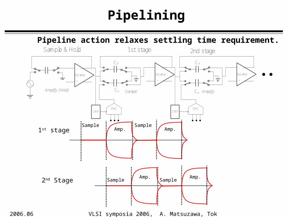
Pipelining
-
-+
+
Op amp
CMPDAC
-
-+
+
Op amp
CMPDAC
-
-+
+
Op amp
Sample & Hold 1st stage 2nd stage
Amplify (Hold) Sample Amplify
Cf
Cs
Cf
Cs
1st stage
2nd Stage
SampleAmp.
SampleAmp.
SampleAmp.
SampleAmp.
Pipeline action relaxes settling time requirement.
2006.06.14.
VLSI symposia 2006, A. Matsuzawa, Tokyo Tech. 43
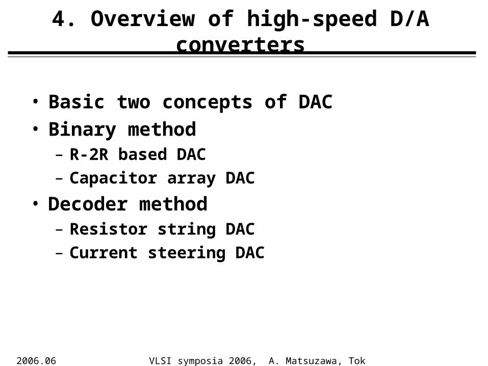
4. Overview of high-speed D/A converters
• Basic two concepts of DAC• Binary method
– R-2R based DAC– Capacitor array DAC
• Decoder method– Resistor string DAC– Current steering DAC
2006.06.14.
VLSI symposia 2006, A. Matsuzawa, Tokyo Tech. 44
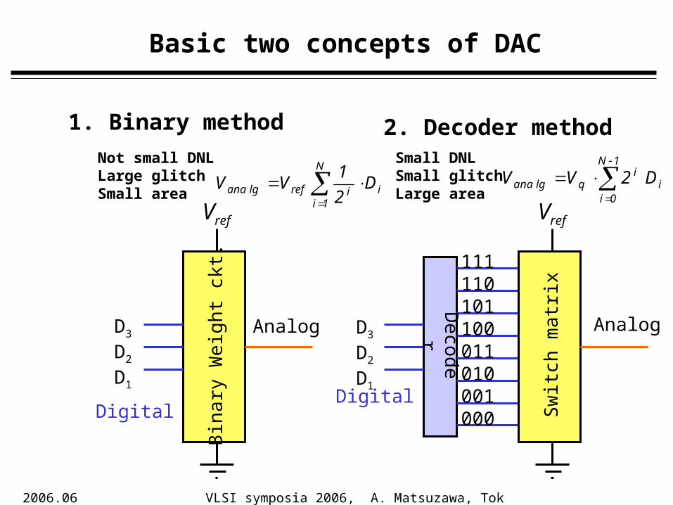
Basic two concepts of DAC
2. Decoder method
111110101100011010001000
De
code
r
Sw
itch
ma
trix
Vref
Digital
AnalogD3
D2
D1
Small DNLSmall glitchLarge area
Bin
ary
We
igh
t ckt
.Vref
1. Binary method
Digital
D3
D2
D1
Analog
Not small DNLLarge glitchSmall area i
N
1iireflgana D
2
1VV
i
1N
0i
iqlgana D2VV
2006.06.14.
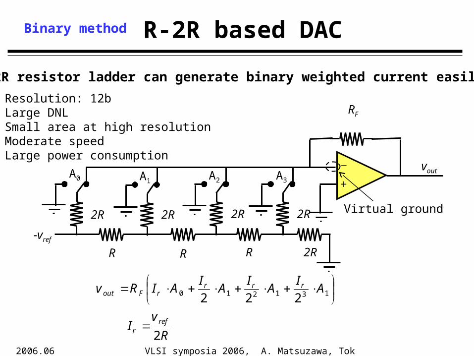
VLSI symposia 2006, A. Matsuzawa, Tokyo Tech. 45
+
vout
2R 2R 2R 2R
A0 A1 A2 A3
RF
-vref
2RRRR
Virtual ground
R
vI
AI
AI
AI
AIRv
refr
rrrrFout
2
222 131210
R-2R based DAC
Resolution: 12bLarge DNLSmall area at high resolutionModerate speedLarge power consumption
Binary method
R-2R resistor ladder can generate binary weighted current easily.
2006.06.14.
VLSI symposia 2006, A. Matsuzawa, Tokyo Tech. 46
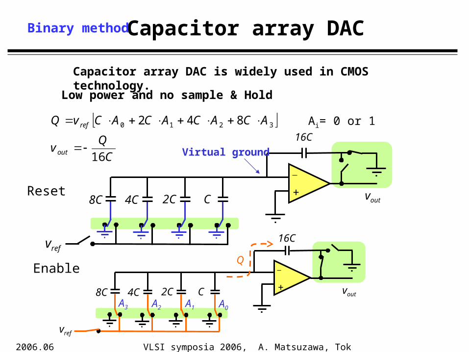
16C
vref
+ vout8C 4C 2C C
CQ
v
ACACACACvQ
out
ref
16
842 3210
+ vout8C 4C 2C C
16C
vref
A0A1A2A3
Q
Reset
Enable
Capacitor array DAC
Virtual ground
Ai= 0 or 1
Binary method
Capacitor array DAC is widely used in CMOS technology.
Low power and no sample & Hold
2006.06.14.
VLSI symposia 2006, A. Matsuzawa, Tokyo Tech. 47
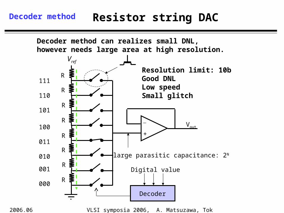
Decoder method Resistor string DAC
Vref
+
Vout
Decoder
R
R
R
R
R
R
R
R
Resolution limit: 10bGood DNLLow speedSmall glitch
large parasitic capacitance: 2N
111
110
101
100
011
010
001
000
Digital value
Decoder method can realizes small DNL, however needs large area at high resolution.
2006.06.14.
VLSI symposia 2006, A. Matsuzawa, Tokyo Tech. 48
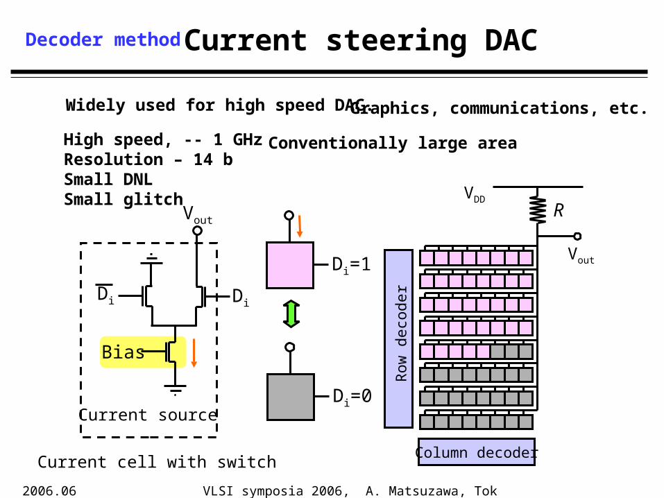
VDD
Bias
Vout
Di Di
Current source
Di=1
Di=0
Vout
Column decoder
R
Row
dec
oder
Current cell with switch
Current steering DAC
Widely used for high speed DAC. Graphics, communications, etc.
High speed, -- 1 GHzResolution – 14 bSmall DNLSmall glitch
Conventionally large area
Decoder method
2006.06.14.
VLSI symposia 2006, A. Matsuzawa, Tokyo Tech. 49
5. Overview of over-sampling sigma-delta data converters
• Sigma-delta modulation method– Over sampling– Noise shaping– Sigma-delta modulator– SNR– Higher order system– Feed forward and feed back compensation– MASH (Multi-stage noise shaping)
2006.06.14.
VLSI symposia 2006, A. Matsuzawa, Tokyo Tech. 50
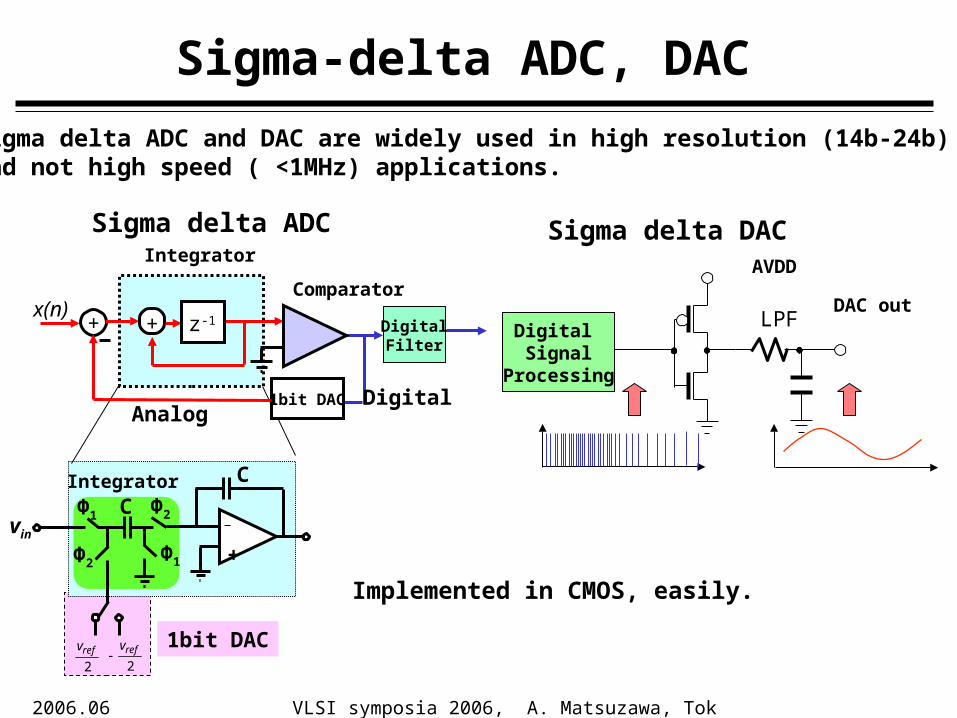
Sigma-delta ADC, DAC
+vin
C
C
Φ1
Φ1
Φ2
Φ2
2refv
2refv
1bit DAC
Integrator
Integrator
+x(n)
+ z-1
1bit DACAnalog
Digital
Comparator
DigitalFilter
Sigma delta ADC Sigma delta DAC
Digital Signal
Processing
AVDD
DAC out
Implemented in CMOS, easily.
Sigma delta ADC and DAC are widely used in high resolution (14b-24b)and not high speed ( <1MHz) applications.
LPF
2006.06.14.
VLSI symposia 2006, A. Matsuzawa, Tokyo Tech. 51
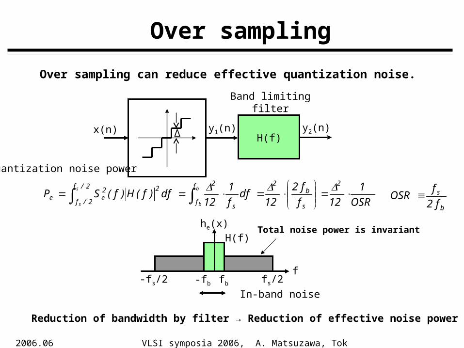
Over sampling
Δx(n) y1(n)H(f)
y2(n)
he(x)
f-fs/2 fs/2
H(f)
-fb fb
OSR1
12ff2
12df
f1
12df)f(H)f(SP
2
s
b2
s
f
f
22/f
2/f
22ee
b
b
s
s
Band limitingfilter
Quantization noise power
Reduction of bandwidth by filter → Reduction of effective noise power
Total noise power is invariant
Over sampling can reduce effective quantization noise.
In-band noise
b
s
f2f
OSR
2006.06.14.
VLSI symposia 2006, A. Matsuzawa, Tokyo Tech. 52
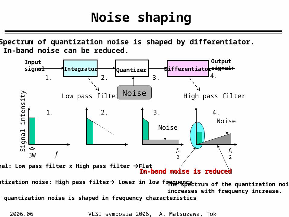
Noise shaping
The spectrum of the quantization noiseincreases with frequency increase.
In-band noise is reducedIn-band noise is reduced
Integrator Quantizer Differentiator
2Sf
2Sf
BW f
Sig
nal i
nten
sity
NoiseNoise
Low pass filter High pass filter
Input signal Output signal
1. 2. 3. 4.
1. 2. 3. 4.
Noise
Quantization noise: High pass filter Lower in low frequency
Signal: Low pass filter x High pass filter Flat
Only quantization noise is shaped in frequency characteristics
Spectrum of quantization noise is shaped by differentiator. In-band noise can be reduced.
2006.06.14.
VLSI symposia 2006, A. Matsuzawa, Tokyo Tech. 53
1z
+Quantizer
1z
+
Integrator Differentiator
1z
+Quantizer
+
IntegratorDifferentiator
1z
Equivalent transform
X(z)
X(z) Y(z)
Y(z)
Q(z)
Q(z)
11 z)z(X
)z(Q)z()z(X)z(Y 11
Sigma-delta modulator
The signal will overflow
No overflow
1 ZQX
Outputsignal
Input signal
Differentiator(High pass filter)
Quantization noise
Sigma-delta modulator shapes the frequency characteristics of the quantization noise
)z(Q)z()z(X)z(Y 11
2006.06.14.
VLSI symposia 2006, A. Matsuzawa, Tokyo Tech. 54
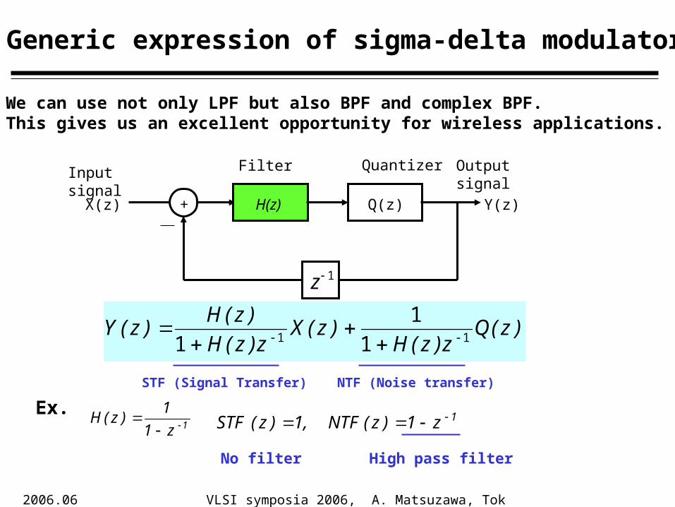
Generic expression of sigma-delta modulator
H(z) Q(z)
Input signal
+
1z
)z(Qz)z(H
)z(Xz)z(H
)z(H)z(Y 11 1
11
Filter
X(z)
Output signal
Y(z)
Quantizer
We can use not only LPF but also BPF and complex BPF.This gives us an excellent opportunity for wireless applications.
STF (Signal Transfer) NTF (Noise transfer)
Ex. 1z1
1)z(H 1z1)z(NTF,1)z(STF
High pass filterNo filter
2006.06.14.
VLSI symposia 2006, A. Matsuzawa, Tokyo Tech. 55
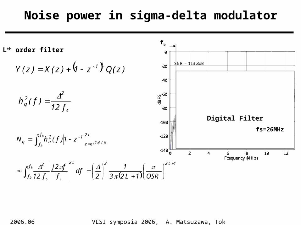
Noise power in sigma-delta modulator
)z(Qz1)z(X)z(YL1
s
22q f12
)f(h
1L22L2
s
f
fs
2
f
f
L2
ez
12qq
OSR1L231
2df
ff2j
f12
z1)f(hN
b
b
b
bfs/f2j
0 2 4 6 8 10 12-140
-120
-100
-80
-60
-40
-20
0
SNR = 113.8dB
Frequency (MHz)dB
FS
0 2 4 6 8 10 12-140
-120
-100
-80
-60
-40
-20
0
SNR = 113.8dB
Frequency (MHz)dB
FS
Digital Filter
fs=26MHz
Lth order filterfb
2006.06.14.
VLSI symposia 2006, A. Matsuzawa, Tokyo Tech. 56
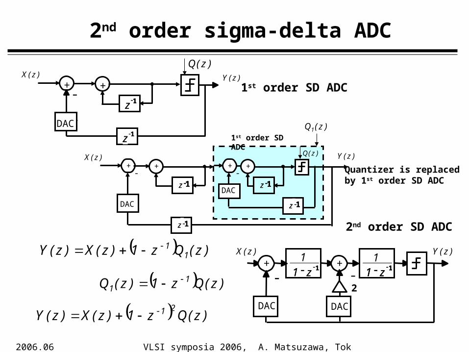
2nd order sigma-delta ADC
1z
+
DAC
1z 1
+
DAC
-++
1z 1z 1
)z(X )z(Y
)z(Q
1z 1z 1
++++-
1z 1z 1
)z(X )z(Y)z(Q
1z 1z 1
++
1z 1z 1
++-
DACDAC
DACDAC
)z(Q1
1st order SD ADC
+
2
11 z
1+
DAC DAC
- -11 z 11 z
+ 11 z 11 z
+
DAC DAC
-
1)z(X )z(Y )z(Qz1)z(X)z(Y 1
1
)z(Qz1)z(Q 11
)z(Qz1)z(X)z(Y21
1st order SD ADC
Quantizer is replaced by 1st order SD ADC
2nd order SD ADC
2006.06.14.
VLSI symposia 2006, A. Matsuzawa, Tokyo Tech. 57
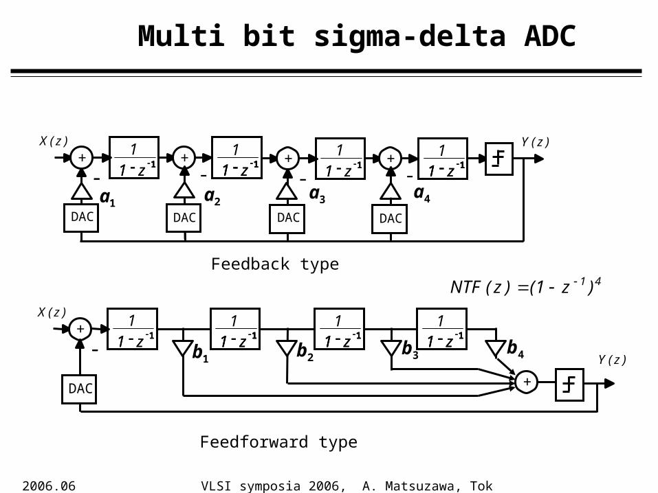
Multi bit sigma-delta ADC
+
DAC
-11 z 11 z
+
DAC
-
1)z(X
++
)z(Y
11 z
111 z 11 z 11
z1
11 z 11 z 11
z1
11 z 11 z
Feedback type
Feedforward type
+ 11 z
1+
DAC DAC
- -11 z 11 z
+ 11 z 11 z
+
DAC DAC
-
1)z(X
+ 11 z
1+
DAC DAC
- -11 z 11 z
+ 11 z 11 z
+
DAC DAC
-
1)z(Y
1a 2a 3a 4a
1b 2b 3b 4b
41)z1()z(NTF
2006.06.14.
VLSI symposia 2006, A. Matsuzawa, Tokyo Tech. 58
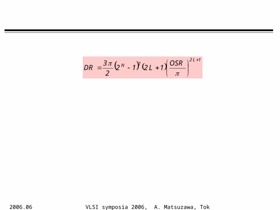
1L2
2N OSR1L212
23
DR
0
204060
80100120140
160180200
1 10 100 1000
Dynam
ic R
ange (dB)
1st
2nd
3rd
4th 5th
OSR
n=1bit
Dynamic range of sigma-delta ADC
Higher order SD modulator seems effective to increase the dynamic range.However it is not easy, because of instability, signal saturation, and thermal noise.
2006.06.14.
VLSI symposia 2006, A. Matsuzawa, Tokyo Tech. 59
Noise-shaping characteristics
103
104
105
106
107
-200
-180
-160
-140
-120
-100
-80
-60
-40
-20
0SNDR = 99.5dBSNR = 100.1dB
In-bandOSR=64200kHz
Dyn
amic
Ran
ge
(dB
)
Frequecy (Hz)
Thermal noise
5th order, 1bit
100dB/dec
103
104
105
106
107
-200
-180
-160
-140
-120
-100
-80
-60
-40
-20
0SNDR = 99.5dBSNR = 100.1dB
In-bandOSR=64200kHz
Dyn
amic
Ran
ge
(dB
)
Frequecy (Hz)
Thermal noise
5th order, 1bit
100dB/dec
103 104 105 106 107-200
-180
-160
-140
-120
-100
-80
-60
-40
-20
0
1st order
20dB/dec
2nd order
40dB/dec
dBF
S
Frequency (Hz)
fs=26MHz
103 104 105 106 107-200
-180
-160
-140
-120
-100
-80
-60
-40
-20
0
1st order
20dB/dec
2nd order
40dB/dec
dBF
S
Frequency (Hz)
fs=26MHz
Higher order sigma-delta modulator can realize higher dynamic range, theoretically.
2006.06.14.
VLSI symposia 2006, A. Matsuzawa, Tokyo Tech. 60
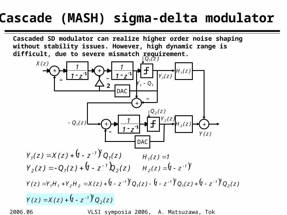
Cascade (MASH) sigma-delta modulator
+
2
11 z
1+
- -11 z 11 z
+ 11 z 11 z
+
DAC
-
1)z(X
)z(Y1
11 z
1+-
11 z 11 z
+
DAC
)z(Y2
+-
)z(H1
)z(H 2 +
)z(Qz1)z(Q)z(Y 21
12
)z(Qz1)z(X)z(Y 1
211
)z(Q1
)z(Q2
11 QY
)z(Q1
)z(Y
1)z(H1
212 z1)z(H
)z(Qz1)z(Qz1)z(Qz1)z(XHYHY)z(Y 231
121
121
2211
)z(Qz1)z(X)z(Y 231
Cascaded SD modulator can realize higher order noise shaping without stability issues. However, high dynamic range is difficult, due to severe mismatch requirement.
2006.06.14.
VLSI symposia 2006, A. Matsuzawa, Tokyo Tech. 61
6. Basic design considerations
• Accuracy– Current mismatch and DAC accuracy
– VT mismatch
– Capacitor mismatch
• Comparator– Offset compensation
• Op-Amp– Gain and GBW– kT/C noise
2006.06.14.
VLSI symposia 2006, A. Matsuzawa, Tokyo Tech. 62
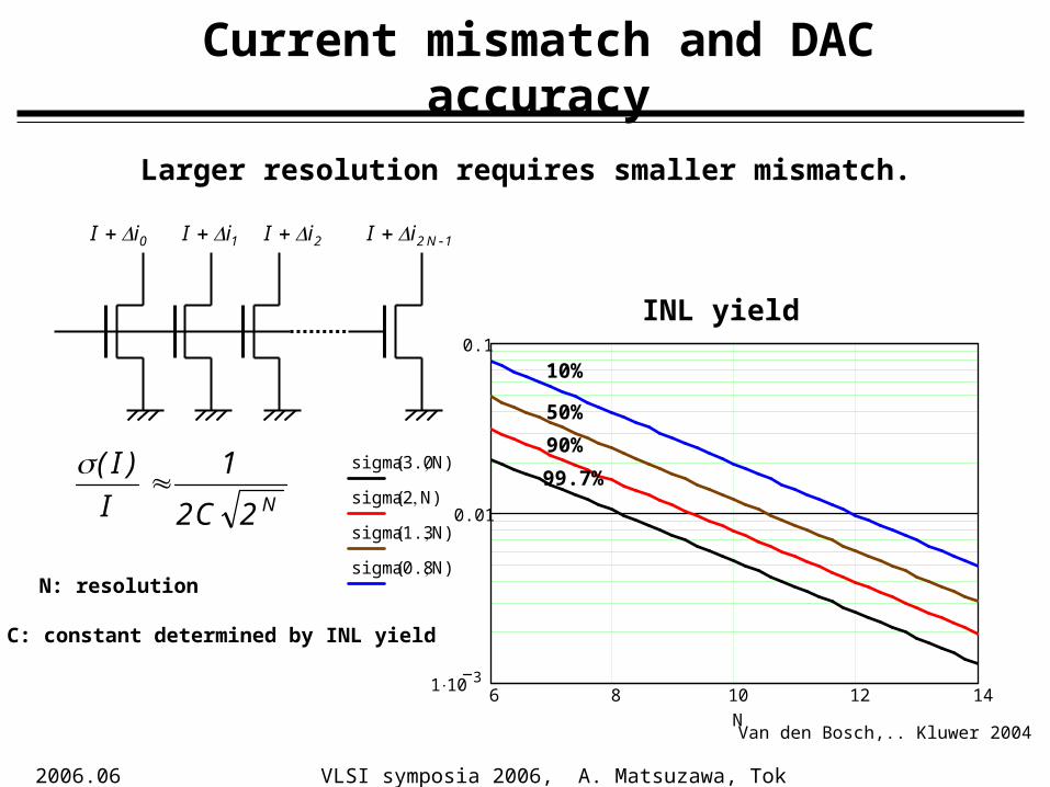
Current mismatch and DAC accuracy
6 8 10 12 14110 3
0.01
0.1
sigma3.0N( )
sigma2 N( )
sigma1.3N( )
sigma0.8N( )
N
90%
50%
10%
99.7%
Van den Bosch,.. Kluwer 2004
INL yield
0iI 1iI 2iI 1N2iI
N2C2
1I
)I(
N: resolution
C: constant determined by INL yield
Larger resolution requires smaller mismatch.
2006.06.14.
VLSI symposia 2006, A. Matsuzawa, Tokyo Tech. 63
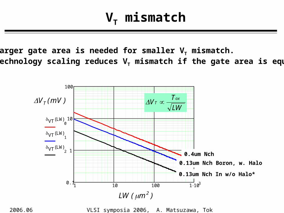
VT mismatch
Larger gate area is needed for smaller VT mismatch.Technology scaling reduces VT mismatch if the gate area is equal.
1 10 100 11030.1
1
10
100
VT LW( )0
VT LW( )1
VT LW( )2
LW
LWT
Vox
T
0.4um Nch
0.13um Nch In w/o Halo*
0.13um Nch Boron, w. Halo
)mV(VT
)m(LW 2
2006.06.14.
VLSI symposia 2006, A. Matsuzawa, Tokyo Tech. 64
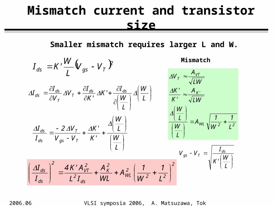
Mismatch current and transistor size
2Tgsds VVL
W'KI
L
W
LWI
'K'K
IV
VI
I dsdsT
T
dsds
LW
LW
'K'K
VVV2
II
Tgs
T
ds
ds
22WL
'K
VTT
L1
W1
A
LW
LW
LW
A'K'K
LW
AV
LW
'K
IVV ds
Tgs
Mismatch
2
222WL
2K
ds2
2VT
2
ds
ds
L
1
W
1A
WLA
IL
A'K4II
Smaller mismatch requires larger L and W.
2006.06.14.
VLSI symposia 2006, A. Matsuzawa, Tokyo Tech. 65
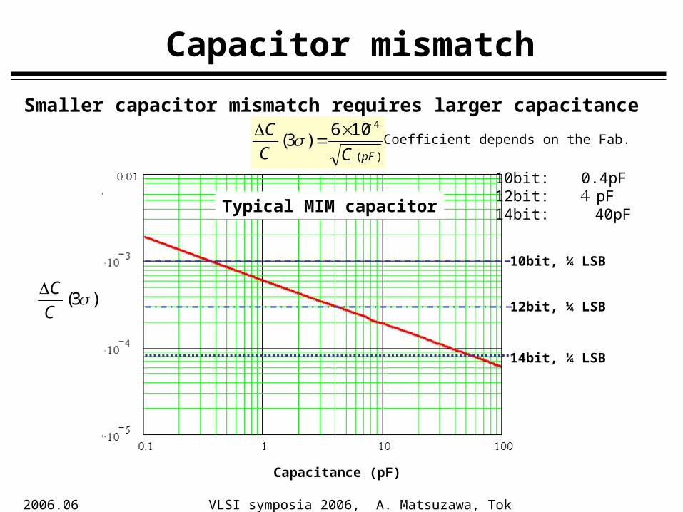
Capacitor mismatch
)(
4106)3(
pFCC
C
)3( C
C
Capacitance (pF)
10bit, ¼ LSB
12bit, ¼ LSB
14bit, ¼ LSB
10bit: 0.4pF12bit: 4 pF14bit: 40pF
Smaller capacitor mismatch requires larger capacitance
Coefficient depends on the Fab.
Typical MIM capacitor
2006.06.14.
VLSI symposia 2006, A. Matsuzawa, Tokyo Tech. 66
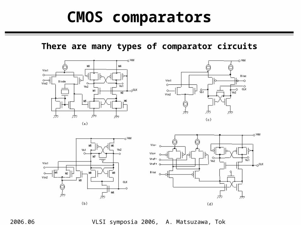
CMOS comparators
There are many types of comparator circuits
2006.06.14.
VLSI symposia 2006, A. Matsuzawa, Tokyo Tech. 67
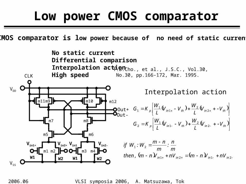
Low power CMOS comparator
VSS
VDD
Vin1+
m2
m7
m9 m10
m3 m4m1
m5 m6
m8
m11 m12
Out+Out-
CLK
W1 W2 W1 W2
thinthinp
thinthinp
VVL
WVV
LW
KG
VVL
WVV
LW
KG
22
11
2
22
11
1
Vin2+ Vin1- Vin2-
2121
21
inininin nVVnmnVVnm,thenmn
:m
nmW:Wif
Interpolation action
No static currentDifferential comparisonInterpolation actionHigh speed
T.B.Cho., et al., J.S.C., Vol.30, No.30, pp.166-172, Mar. 1995.
A CMOS comparator is low power because of no need of static current.
2006.06.14.
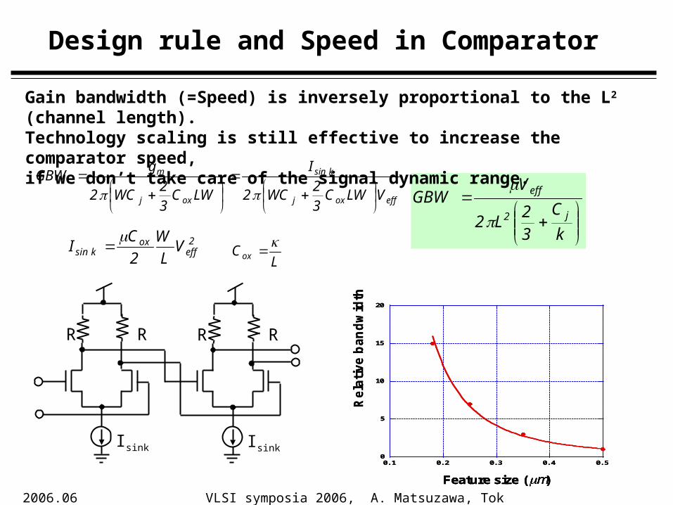
VLSI symposia 2006, A. Matsuzawa, Tokyo Tech. 68
Isink
R R
Isink
R R
effoxj
ksin
oxj
m
VLWC32
WC2
I
LWC32
WC2
gGBW
2eff
oxksin V
LW
2C
I
L
Cox
k
C
32
L2
VGBW
j2
eff
0
5
10
15
20
0.1 0.2 0.3 0.4 0.5
Re
lati
ve
ba
nd
wid
th
Feature size ( )m
0
5
10
15
20
0.1 0.2 0.3 0.4 0.5
Re
lati
ve
ba
nd
wid
th
Feature size ( )mFeature size ( )m
Design rule and Speed in Comparator
Gain bandwidth (=Speed) is inversely proportional to the L2 (channel length).Technology scaling is still effective to increase the comparator speed, if we don’t take care of the signal dynamic range.
2006.06.14.
VLSI symposia 2006, A. Matsuzawa, Tokyo Tech. 69
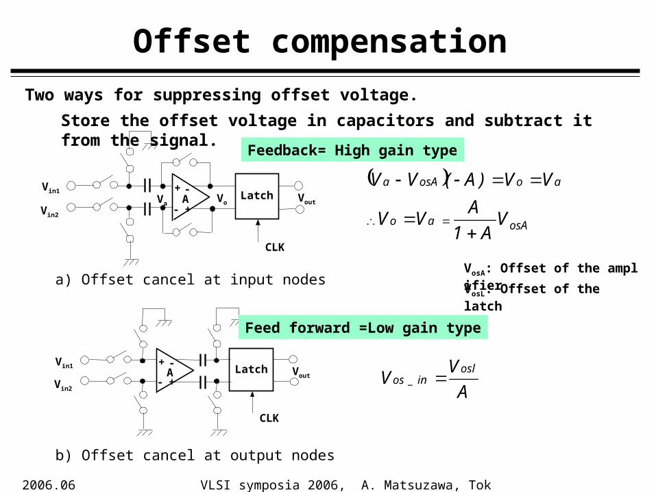
Offset compensation
CLK
LatchVin1
Vin2
A Vout
+
-
-
+Va
Vo
CLK
LatchVin1
Vin2
VoutA+
-
-
+
Store the offset voltage in capacitors and subtract it from the signal.
osAao
aoosAa
VA1
AVV
VV)A(VV
AV
Vosl
in_os
VosA: Offset of the amplifier
VosL: Offset of the latcha) Offset cancel at input nodes
b) Offset cancel at output nodes
Feedback= High gain type
Feed forward =Low gain type
Two ways for suppressing offset voltage.
2006.06.14.
VLSI symposia 2006, A. Matsuzawa, Tokyo Tech. 70
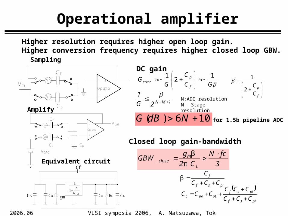
Operational amplifier
-
-+
+
Op amp
Cf
Cs Cp
Vout
VDAC
Vn
Vn
-
-+
+
Op amp
Cf
Cs
VinVn
Vn
Sampling
Amplify
GC
C
GG
f
perror
12
1
f
p
C
C2
1
106)( NdBG
N:ADC resolutionM: Stage resolution
1MN2G1
for 1.5b pipeline ADC
DC gain
Cf
Cs Cpi gm Cpo COLRL2
1
1
p
sω
Equivalent circuit
pisf
f
CCC
C
β
pisf
pisfoLpoL CCC
CCCCCC
3fcN
C2g
GBWL
mclose_
πβ
Closed loop gain-bandwidth
Higher resolution requires higher open loop gain.Higher conversion frequency requires higher closed loop GBW.
2006.06.14.
VLSI symposia 2006, A. Matsuzawa, Tokyo Tech. 71
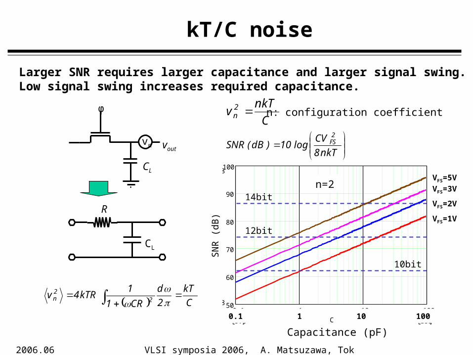
kT/C noise
R
CL
Larger SNR requires larger capacitance and larger signal swing.Low signal swing increases required capacitance.
CL
vout
φ
vn
0.1 1 10 10050
60
70
80
90
10095.918
51.938
SNRC 1 2 C
SNRC 2 2 C
SNRC 3 2 C
SNRC 5 2 C
1000.1 C
14bit
12bit
10bit
0.1 1 10 100
VFS=5V
VFS=3V
VFS=2V
VFS=1V
n=2
SN
R (
dB)
Capacitance (pF)
CkT
2d
CR1
1kTR4v
22n
CnkT
v2n n: configuration coefficient
nkT8CV
log10)dB(SNR2FS
2006.06.14.
VLSI symposia 2006, A. Matsuzawa, Tokyo Tech. 72
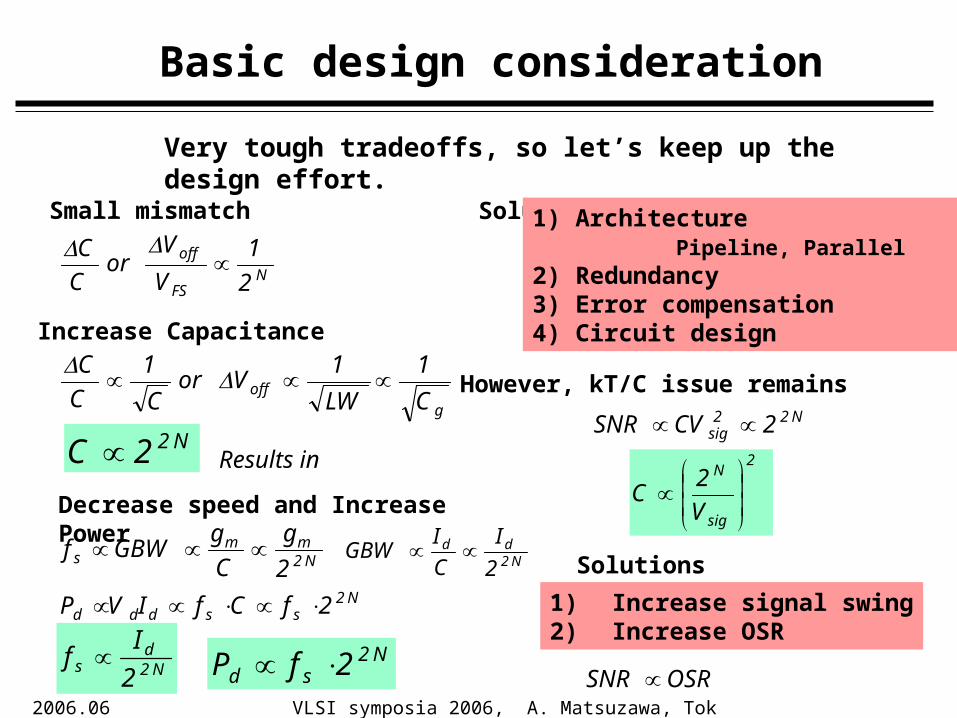
Basic design consideration
Small mismatch
NFS
off
2
1V
Vor
CC
goff
C
1
LW
1Vor
C
1CC
Increase Capacitance
Decrease speed and Increase Power
N2mm
s 2
gCg
GBWf N2
dd
2
ICI
GBW
N2ssddd 2fCfIVP
N22C
Solutions1) Architecture Pipeline, Parallel2) Redundancy3) Error compensation4) Circuit design
However, kT/C issue remainsN22
sig 2CVSNR 2
sig
N
V2
C
N2d
s 2
If N2
sd 2fP
Solutions
1) Increase signal swing2) Increase OSR
OSRSNR
Very tough tradeoffs, so let’s keep up the design effort.
Results in
2006.06.14.
VLSI symposia 2006, A. Matsuzawa, Tokyo Tech. 73
Acknowledgement
• The author thanks Mr. T. Matsuura from Renesus for some slides provision.
2006.06.14.
VLSI symposia 2006, A. Matsuzawa, Tokyo Tech. 74
Study-aid books
• B. Razavi, “Data conversion system design,” IEEE press.
• P. E. Allen and D. R. Holberg, “ CMOS Analog Circuit Design,” 2nd Edition, OXFORD University Press.
• D. A. Johns and K. Martin, “Analog integrated circuit design,” John Wiley & Sons.
• R. J. Baker, “ CMOS mixed-signal circuit design,” IEEE Press.
• R.van de Plassche, “CMOS Integrated Analog-to-Digital and Digital-to-Analog Converters,” 2nd Edition, Kluwer Academic Publishers.
• M. Gustavsson, J. J. Wikner and N. N. Tan, “CMOS data converters for communications,” Kluwer Academic Publishers.
• C. Shi and M. Ismail, ”Data converters for wireless standards,” Kluwer Academic Publishers.
• A. Rodriguez-Vazquez, F. Mederio, and E. Janssens, “CMOS Telecom Data Converters,” Kluwer Academic Publishers.