Ioan Moga - Voievodatul Transilvaniei - Fapte Si Interpretari
Upload
donald-mortonCategory
view
222download
4
1
Lecture on
Field Effect Transistor (FET)
by:-Uttampreet Singh
Lecturer-Electrical Engg.Govt. Polytechnic College, G.T.B.garh, Moga
2
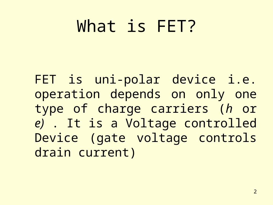
What is FET?
FET is uni-polar device i.e. operation depends on only one type of charge carriers (h or e) . It is a Voltage controlled Device (gate voltage controls drain current)
3
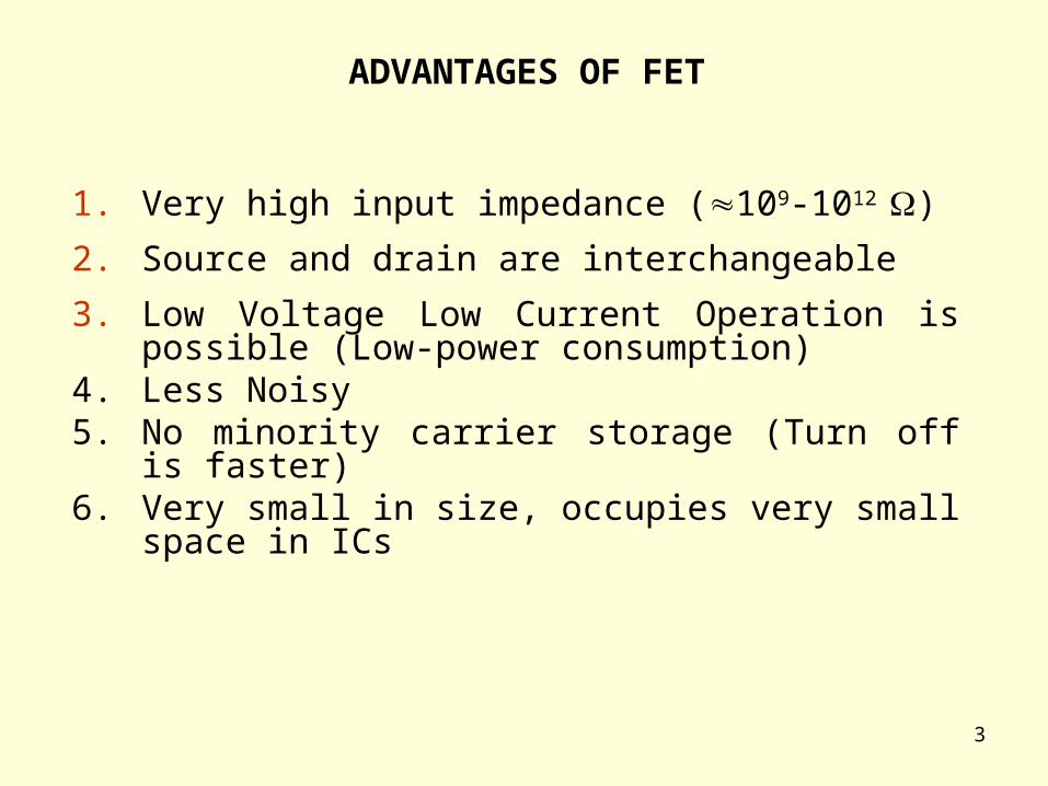
1. Very high input impedance (109-1012 )
2. Source and drain are interchangeable
3. Low Voltage Low Current Operation is possible (Low-power consumption)
4. Less Noisy 5. No minority carrier storage (Turn off is faster) 6. Very small in size, occupies very small space
in ICs
ADVANTAGES OF FET
4
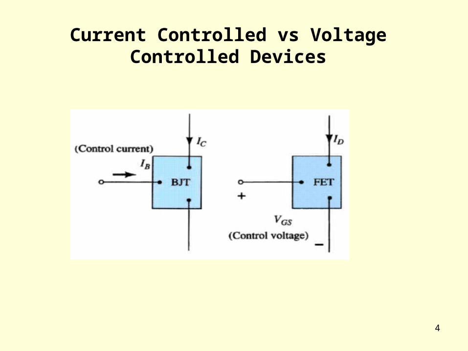
Current Controlled vs Voltage Controlled Devices

5
Types of Field Effect Transistors (The Classification)
» JFET
MOSFET (IGFET)
n-Channel JFET
p-Channel JFET
n-Channel EMOSFET
p-Channel EMOSFET
Enhancement MOSFET
Depletion MOSFET
n-Channel DMOSFET
p-Channel DMOSFET
FETFETFET » JFET
MOSFET (IGFET)
FET » JFET
MOSFET (IGFET)
FET
6
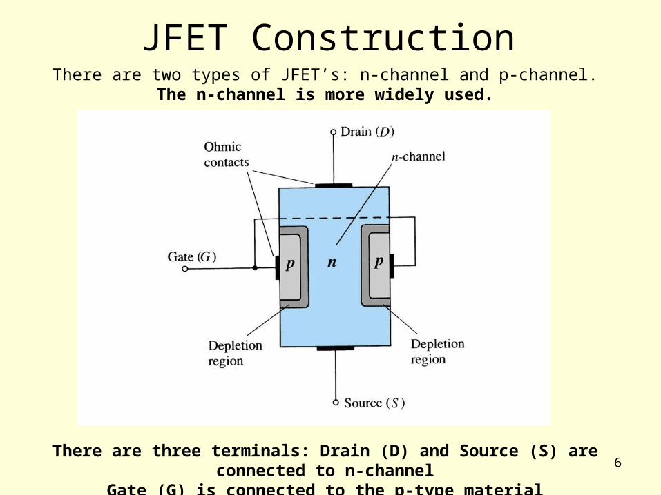
JFET ConstructionThere are two types of JFET’s: n-channel and p-channel.
The n-channel is more widely used.
There are three terminals: Drain (D) and Source (S) are connected to n-channelGate (G) is connected to the p-type material
7
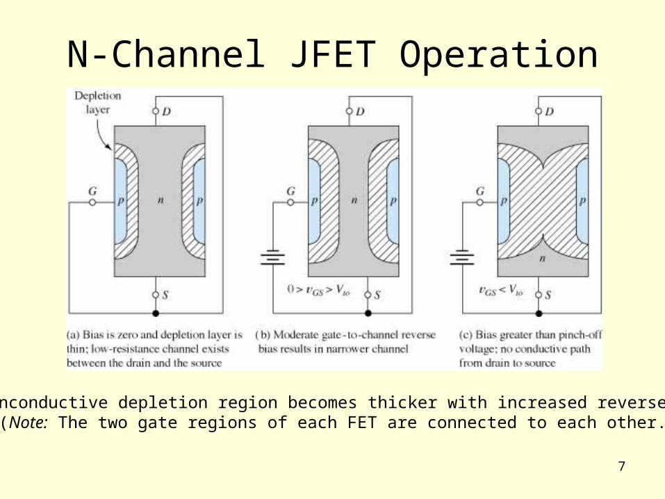
The nonconductive depletion region becomes thicker with increased reverse bias. (Note: The two gate regions of each FET are connected to each other.)
N-Channel JFET Operation

8
Gate
Drain
Source
SYMBOLS
n-channel JFET
Gate
Drain
Source
p-channel JFET
9
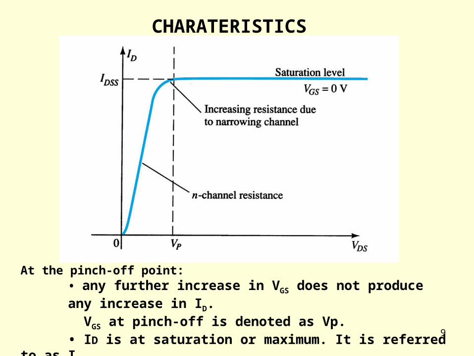
CHARATERISTICS
At the pinch-off point: • any further increase in VGS does not produce any increase in ID. VGS at pinch-off is denoted as Vp. • ID is at saturation or maximum. It is referred to as IDSS.
10
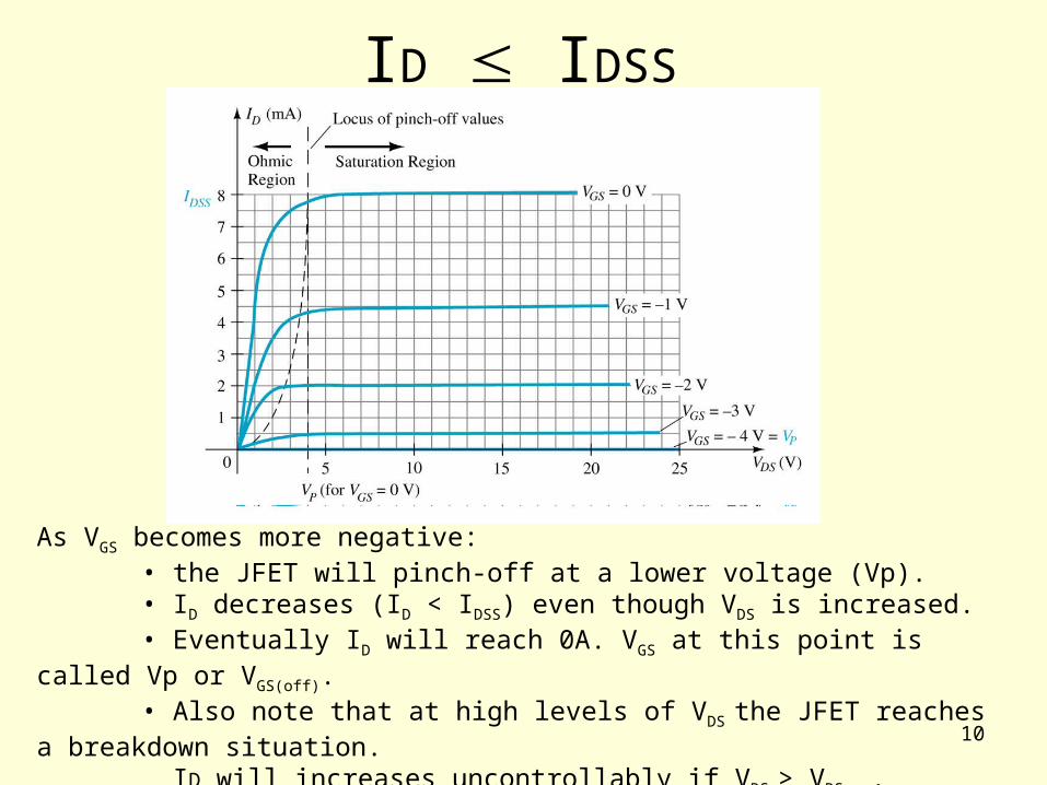
ID IDSS
As VGS becomes more negative:• the JFET will pinch-off at a lower voltage (Vp).• ID decreases (ID < IDSS) even though VDS is increased.• Eventually ID will reach 0A. VGS at this point is called Vp or VGS(off).• Also note that at high levels of VDS the JFET reaches a breakdown situation. ID will increases uncontrollably if VDS > VDSmax.
11
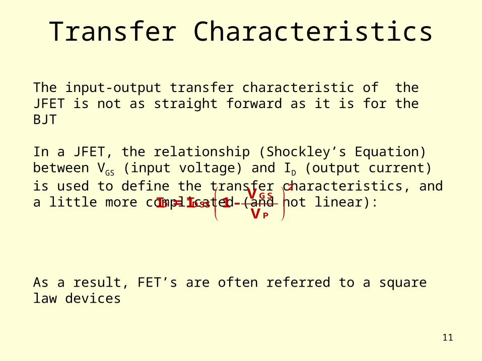
Transfer Characteristics
The input-output transfer characteristic of the JFET is not as straight forward as it is for the BJT
In a JFET, the relationship (Shockley’s Equation) between VGS (input voltage) and ID (output current) is used to define the transfer characteristics, and a little more complicated (and not linear):
As a result, FET’s are often referred to a square law devices
2GS
D DSSP
V I = I 1 -
V

12
Transfer (Transconductance) Curve
From this graph it is easy to determine the value of ID for a given value of VGS
It is also possible to determine IDSS and VP by looking at the knee where VGS is 0

13
Case Construction and Terminal Identification

14
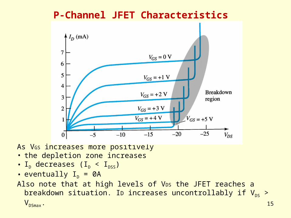
p-Channel JFET
p-Channel JFET operates in a similar manner as the n-channel JFET except the voltage polarities and current directions are reversed
15
P-Channel JFET Characteristics
As VGS increases more positively• the depletion zone increases• ID decreases (ID < IDSS)• eventually ID = 0AAlso note that at high levels of VDS the JFET reaches a breakdown situation. ID increases
uncontrollably if VDS > VDSmax.
16
MOSFET(Metal Oxide Semiconductor FET)
17
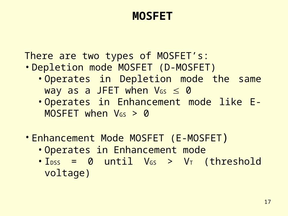
MOSFET
There are two types of MOSFET’s:• Depletion mode MOSFET (D-MOSFET)
• Operates in Depletion mode the same way as a JFET when VGS 0
• Operates in Enhancement mode like E-MOSFET when VGS > 0
• Enhancement Mode MOSFET (E-MOSFET)• Operates in Enhancement mode• IDSS = 0 until VGS > VT (threshold voltage)
18
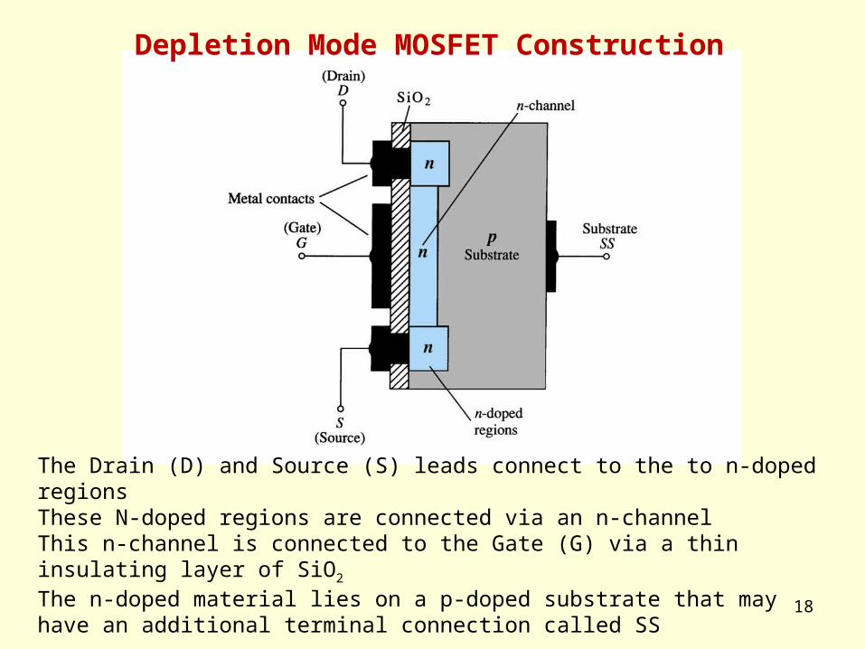
Depletion Mode MOSFET Construction
The Drain (D) and Source (S) leads connect to the to n-doped regionsThese N-doped regions are connected via an n-channelThis n-channel is connected to the Gate (G) via a thin insulating layer of SiO2
The n-doped material lies on a p-doped substrate that may have an additional terminal connection called SS

19
D-MOSFET Symbols

20
Basic Operation
A D-MOSFET may be biased to operate in two modes: the Depletion mode or the Enhancement mode

21
p-Channel Depletion Mode MOSFET
The p-channel Depletion mode MOSFET is similar to the n-channel except that the voltage polarities and current directions are reversed
22
Enhancement ModeMOSFET’s
23
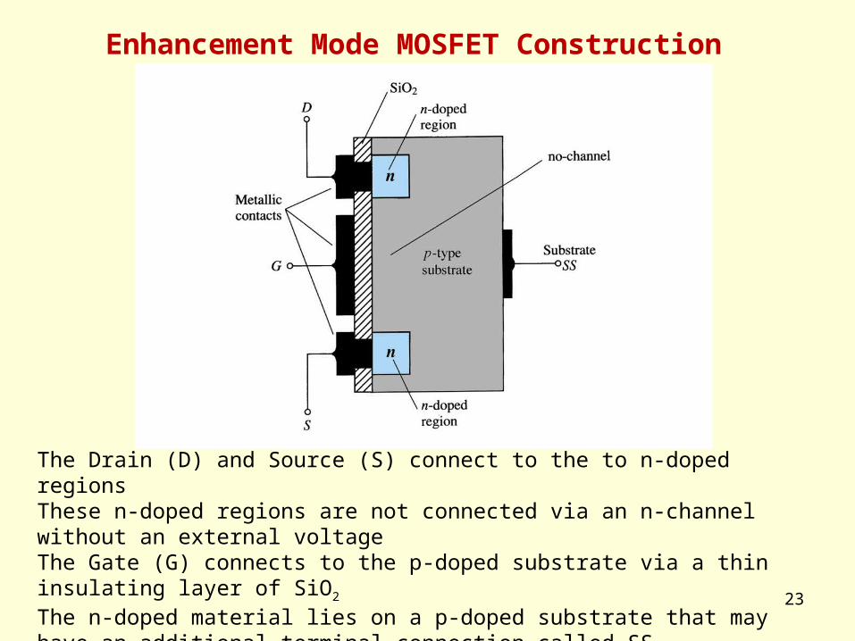
Enhancement Mode MOSFET Construction
The Drain (D) and Source (S) connect to the to n-doped regionsThese n-doped regions are not connected via an n-channel without an external voltageThe Gate (G) connects to the p-doped substrate via a thin insulating layer of SiO2
The n-doped material lies on a p-doped substrate that may have an additional terminal connection called SS
24
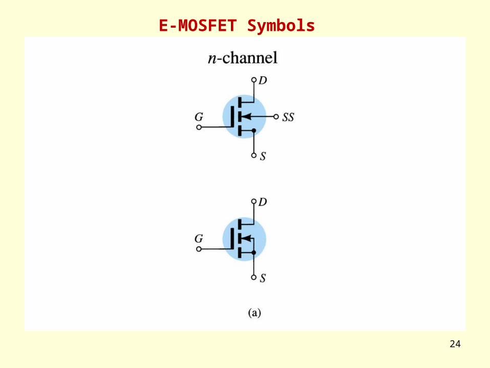
E-MOSFET Symbols
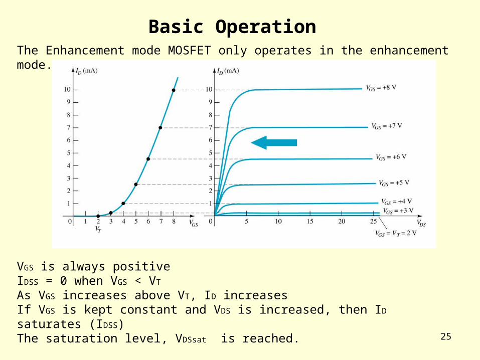
25
Basic OperationThe Enhancement mode MOSFET only operates in the enhancement mode.
VGS is always positiveIDSS = 0 when VGS < VT
As VGS increases above VT, ID increasesIf VGS is kept constant and VDS is increased, then ID saturates (IDSS)The saturation level, VDSsat is reached.
26
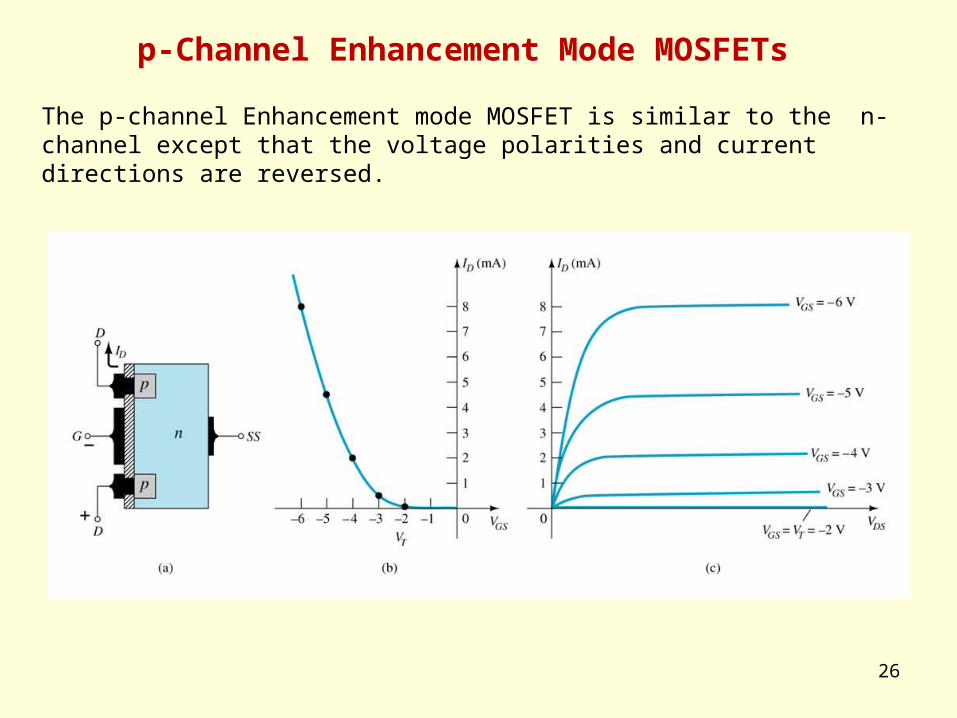
p-Channel Enhancement Mode MOSFETs
The p-channel Enhancement mode MOSFET is similar to the n-channel except that the voltage polarities and current directions are reversed.

27
Summary Table
JFET D-MOSFET E-MOSFET

28