MLN-SERIES(MLN10005D,PN-12159) Product Datasheetaddendum J-STD-001FS FIT:
14
MLN-Series MLN10005D Part Number:12159 HIGH RELIABILITY RADIATION HARDENED LOW POWER DC-DC CONVERTER MLN10005D Description The MLN series is a family of high reliability dual output, low power DC/DC converters designed for space applications. The design lifetime is 18 year and the converters are designed for radiation environments encountered by geostationary earth orbit satellites, deep space probes and communication systems. It offers good tolerance to total ionizing dose, single event effects, and environmental stresses such as temperature extremes, mechanical shock and vibration. All components are fully derated to meet the requirements of EEE-INST- 002 (NASA) and ECSS-Q-30-11A (ESA). Features include isolated telecommand and telemetry interface, internal EMI filter and under voltage protection (UVP) and the design can be tailored to fit all major satellite platforms. Due to excellent output stability and sequencing between outputs, the MLN-series is well suited for use in RF- applications where low noise, high output voltage accuracy and high CS attenuation is required. Each converter is provided as a complete board assembly for installation into the host equipment Extensive documentation including worst case analysis, radiation susceptibility, thermal analysis, stress analysis, and reliability analysis is available. 1 2020-02-28 PD-97955 100V Input, Dual Output Applications General low power space applications Low power RF systems (like LNA) Master reference oscillators International Rectifier HiRel Products, Inc. Features General O/P 1: +1.5V to +15V, up to 750mA or 4W O/P 2: -1.5V to -15V, up to 200mA, or 1W Input ranges can be accommodated within an overall range from 20VDC to 100VDC Short circuit and overload protection Input under-voltage protection Output sequencing: Neg. O/P rises first at turn- on and falls last at turn off Galvanic isolation, >10MΩ @ 100VDC Telecommand/Telemetry Isolated On/Off control via high level pulse command (latching relay) On/Off Status telemetry (relay contact type) Output status telemetry (Analog/bi-level) EMC Output Ripple: <1mVrms (100Hz – 50MHz) CS rejection input to outputs: > 80dB (50Hz – 100kHz) Internal EMI filter: Meets conducted emission requirements of major satellite power buses Radiation TID Rating : 100k rad(Si) SEE Rating: 60 MeV/cm 2 /mg Quality Meets derating requirements of EEE-INST-002 and ECSS-Q-30-11A Workmanship per J-STD-001 with space addendum J-STD-001FS FIT: <70 @ 35°C, SF env. Design life: 18 years Mechanical Small dimensions: 60x50x18mm (LxBxH) Vibration and shock resistant Low weight, < 45 grams Board is coated with ARATHANE-5750
Transcript of MLN-SERIES(MLN10005D,PN-12159) Product Datasheetaddendum J-STD-001FS FIT:

MLN-Series
MLN10005D
Part Number:12159
HIGH RELIABILITY
RADIATION HARDENED
LOW POWER
DC-DC CONVERTER
MLN10005D
Description The MLN series is a family of high reliability dual output, low power DC/DC converters designed for space applications.
The design lifetime is 18 year and the converters are designed for radiation environments encountered by geostationary earth orbit satellites, deep space probes and communication systems.
It offers good tolerance to total ionizing dose, single event effects, and environmental stresses such as temperature extremes, mechanical shock and vibration. All components are fully derated to meet the requirements of EEE-INST-002 (NASA) and ECSS-Q-30-11A (ESA).
Features include isolated telecommand and telemetry interface, internal EMI filter and under voltage protection (UVP) and the design can be tailored to fit all major satellite platforms.
Due to excellent output stability and sequencing between outputs, the MLN-series is well suited for use in RF-applications where low noise, high output voltage accuracy and high CS attenuation is required.
Each converter is provided as a complete board assembly for installation into the host equipment
Extensive documentation including worst case analysis, radiation susceptibility, thermal analysis, stress analysis, and reliability analysis is available.
1 2020-02-28
PD-97955
100V Input, Dual Output
Applications General low power space applications
Low power RF systems (like LNA)
Master reference oscillators
International Rectifier HiRel Products, Inc.
Features General
O/P 1: +1.5V to +15V, up to 750mA or 4W
O/P 2: -1.5V to -15V, up to 200mA, or 1W
Input ranges can be accommodated within an overall range from 20VDC to 100VDC
Short circuit and overload protection
Input under-voltage protection
Output sequencing: Neg. O/P rises first at turn-on and falls last at turn off
Galvanic isolation, >10MΩ @ 100VDC Telecommand/Telemetry
Isolated On/Off control via high level pulse command (latching relay)
On/Off Status telemetry (relay contact type)
Output status telemetry (Analog/bi-level) EMC
Output Ripple: <1mVrms (100Hz – 50MHz)
CS rejection input to outputs: > 80dB (50Hz – 100kHz)
Internal EMI filter: Meets conducted emission requirements of major satellite power buses
Radiation
TID Rating : 100k rad(Si)
SEE Rating: 60 MeV/cm2/mg
Quality
Meets derating requirements of EEE-INST-002 and ECSS-Q-30-11A
Workmanship per J-STD-001 with space addendum J-STD-001FS
FIT: <70 @ 35°C, SF env.
Design life: 18 years Mechanical
Small dimensions: 60x50x18mm (LxBxH)
Vibration and shock resistant
Low weight, < 45 grams
Board is coated with ARATHANE-5750

MLN10005D (100V Input, Dual Output)
2 2020-02-28 International Rectifier HiRel Products, Inc.
1 Specification Overview, MLN10005D, PN12159
Section 2 in this datasheet presents the generic design envelope, while this section present the data for part number 12159.
Absolute Maximum Ratings Recommended Operating Conditions
Input Voltage -0.5VDC to +120VDC Input voltage range (note 9) +97VDC to +103VDC
Output power Internally limited Output power 0 to 4W
Operating mounting point temperature
-55°C to +100°C Operating mounting point temperature (note 9)
-35°C to +70°C*
Storage temperature -55°C to +125°C Cold start temperature (note 9) -40°C
For Notes to Electrical Performance Characteristics, refer to page 5
* The DC/DC converter will keep derating as per EEE-INST-002 and ECSS-Q-30-11A. In order to respect the required component temperatures, the host chassis must provide a good thermal conductive path through the fixation screws .
1.1 Electrical Performance Characteristics
Parameter Conditions
Conditions
-35°C TC +70°C VIN = 100V DC ± 0.5%, CL = 0 unless otherwise specified
Limits
Unit Min Nom Max
Fundamental Characteristics
Input voltage (VIN) 97 100 103 V
Output voltage (VOUT1 / VOUT2) +5V -5V
+5V -5V
+5V -5V
1 1 2 2 3 3
0% ≤ IOUT = 100% rated load
Note 1
0% ≤ IOUT = 100% rated load Note 1
0% ≤ IOUT = 100% rated load
Note 1
+4.975 -4.975
+4.950 -4.950
+4.925 -4.925
+5.00 -5.00
+5.025 -5.025
+5.050 -5.050
+5.075 -5.075
V
Output power (POUT1 / POUT2 ) +5V -5V
1,2,3
3.75 0.25
W
Output current (IOUT1 / IOUT2) +5V -5V
1,2,3 Note 1 0 0
750 50
mA
Current Limit Point (CLOUT1 / CLOUT2)
+5V -5V
1,2,3 Note 1
800 80
1000 110
mA
Input current (IIN)
1,2,3 Commanded Off Commanded On, IOUT = 0 Maximum load Failure mode (short circuit)
1.2 10 57
2 15 65 85
mA
Switching frequency (FS) 1,2,3 Notes 1, 7 129 140 151 kHz
Efficiency (EFF)
1,2 1,2 1,2 3
1/3 load 2/3 load Full load
Full load, EOL
54 61 62 61
60 65 66 64
%
Detailed Output Characteristics
Line regulation (VRLINE) Both Output 1,2,3
VIN = 97, 100, 103 Volts IOUT = 0, 50%, 100% rated, Note 4
-5
+5 mV
Load regulation (VRLOAD) Both Output 1,2,3
IOUT = 0, 50%, 100% rated, Note 4 VIN = 97, 100, 103 Volts
-5
+5 mV

MLN10005D (100V Input, Dual Output)
3 2020-02-28 International Rectifier HiRel Products, Inc.
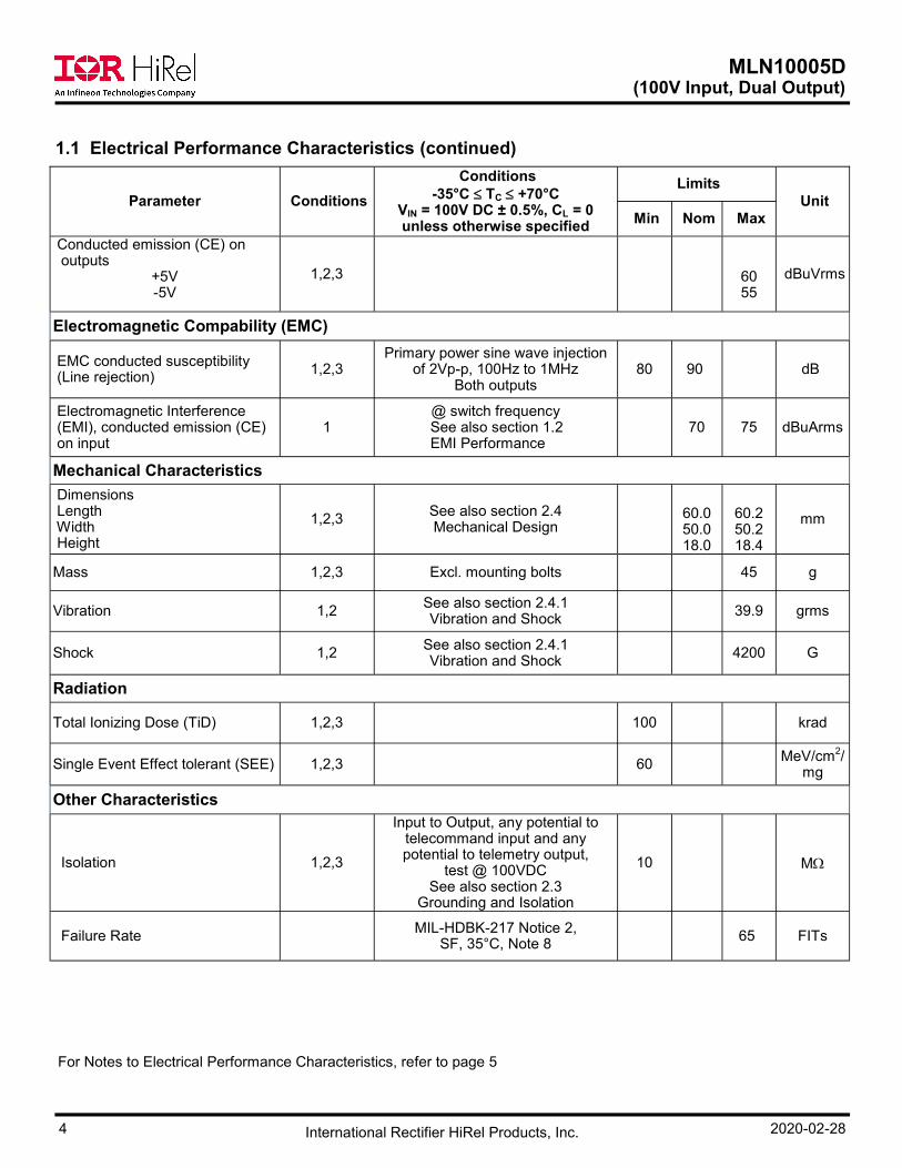
1.1 Electrical Performance Characteristics (continued)
Parameter Conditions
Conditions
-35°C TC +70°C VIN = 100V DC ± 0.5%, CL = 0 unless otherwise specified
Limits
Unit Min Nom Max
Cross regulation (VRCROSS) 1,2,3
Both Output, Note 1 VIN = 97, 100, 103 Volts
-5.0
+5.0
mV
Output ripple (VRIP) +5V -5V
+5V -5V
1
1,2
Frequency domain 100Hz – 50MHz
Time domain 100Hz – 50MHz Notes 1, 2
1 1
30 30
mVrms
mVp-p
Output response to step load changes (VTLD)
+5V -5V
1,2,3
20% to 100% Load, Notes 3,4
-100 -50
+100 +50
mVpk
Recovery time, step load changes (TTLD) 1,2,3 20% to 100% Load, Notes 3,4 2.5 ms
Output response to Single Event Transients (VSET)
+5V -5V
1,2,3
In 20% to 100% rated load, Note 3
200
100
mVpk
Recovery time, Single Event Transients (VSET)
+5V -5V
1,2,3
In 20% to 100% rated load, Note 3 -350 -100
+100 +150
µs
Turn-on Response Overshoot (VOS)
+5V -5V
Turn-on Delay (TDLY)
1,2,3 Notes 1,5
2.0
50 300 10
mV
ms
Output Sequencing Turn-on delay -5V to +5V Turn-off delay +5V to -5V
1,2,3
Note 1 See section 2.2.5 for details
5V <10% of nom, -5V >90% of nom. 5V <10% of nom, -5V >90% of nom.
2 1
12 8
ms
Capacitive load (CL) 1,2,3
Notes 1, 6 Max capacitive load, each output
100 µF
Telemetry & Telecommand (TM & TC)
Telecommand I/F ON command pulse Neg. Pulse Voltage Pulse duration
1,2,3 Note 10 +22.3 -40 10
+26
+30 +0.5 1000
V
ms Status Telemetry Converter On Converter Off
1,2,3 Note 10
Closed contact Open contact 1
10
Ω MΩ
Bilevel Telemetry 1,2,3
Output impedance = 1kohm No load voltage
4.9 5.0 5.1 V
Undervoltage Protection (UVP)
Under voltage Protection Trig level – turn off Hysteresis
1,2,3 0% ≤ IOUT ≤ 100% of rated load 77 2.0
81.4 2.4
84.5 2.9
V
For Notes to Electrical Performance Characteristics, refer to page 5
MLN10005D (100V Input, Dual Output)
4 2020-02-28 International Rectifier HiRel Products, Inc.
1.1 Electrical Performance Characteristics (continued)
Parameter Conditions
Conditions
-35°C TC +70°C VIN = 100V DC ± 0.5%, CL = 0 unless otherwise specified
Limits
Unit
Min Nom Max
Conducted emission (CE) on outputs
+5V -5V
1,2,3
60 55
dBuVrms
Electromagnetic Compability (EMC)
EMC conducted susceptibility (Line rejection)
1,2,3 Primary power sine wave injection
of 2Vp-p, 100Hz to 1MHz Both outputs
80 90 dB
Electromagnetic Interference (EMI), conducted emission (CE) on input
1 @ switch frequency
See also section 1.2 EMI Performance
70 75 dBuArms
Mechanical Characteristics
Dimensions Length Width Height
1,2,3 See also section 2.4 Mechanical Design
60.0 50.0 18.0
60.2 50.2 18.4
mm
Mass 1,2,3 Excl. mounting bolts 45 g
Vibration 1,2 See also section 2.4.1 Vibration and Shock
39.9 grms
Shock 1,2 See also section 2.4.1 Vibration and Shock
4200 G
Radiation
Total Ionizing Dose (TiD) 1,2,3 100 krad
Single Event Effect tolerant (SEE) 1,2,3 60 MeV/cm
2/
mg
Other Characteristics
Isolation 1,2,3
Input to Output, any potential to telecommand input and any potential to telemetry output,
test @ 100VDC See also section 2.3
Grounding and Isolation
10 M
Failure Rate MIL-HDBK-217 Notice 2,
SF, 35°C, Note 8 65 FITs
For Notes to Electrical Performance Characteristics, refer to page 5

MLN10005D (100V Input, Dual Output)
5 2020-02-28 International Rectifier HiRel Products, Inc.
Notes: Electrical Performance Characteristics Table General: All parameters are specified within recommended operating conditions unless otherwise stated. 1. Parameter is analyzed and tested.
2. Guaranteed for a DC to 50MHz bandwidth. Tested using a 10.7MHz bandwidth.
3. Load step transition time ≥ 10 µs.
4. Recovery time is measured from the initiation of the transient to where VOUT has returned to within 90% of its steady state value.
5. Turn-on delay time from application of telecommand pulse to the point where output 2 >90% of nominal output voltage.
6. Capacitive load may be any value from 0 to the maximum limit without compromising the output sequencing performance. A capacitive load in excess of the maximum limit may influence the output sequencing performance and start-up time, but the converter operation and dc performance will remain intact.
7. The switching frequency and 1st and 2nd harmonic of the input ripple is tested on every unit.
8. MIL-HDBK-217Fn2 stress-dependent method is used with 2 exceptions: For soldering a fixed failure rate at 0.035FIT is used and for power MOSFETs the dissipated power (instead of rated power) is used for the Pr parameter. 1 FIT is 1 failure in 109 hours.
9. The converter meets full derating per EEE-INST-002 and ECSS-Q-30-11A with the following exception: For Schottky diode JANS1N5819 a maximum derated junction temperature of +110°C. For EEE-INST-002 it is required that ceramic capacitors with a voltage stress below 10V shall be rated for minimum 100V – in the design such capacitors is rated for 50V minimum.
10. Generic TM/TC circuit and configuration for specific part number is presented in section number 2.2.3 Telecommand and Status Telemetry.
Electrical Performance Characteristics - Definition of Conditions
Conditions Definition Comment
1 BOL @ +25°C interface temperature Initial setting
2 BOL @ -35°C to +70°C interface temperature Initial setting and worst case temperature variation
3 EOL @ -35°C to +70°C interface temperature Worst case performance including initial setting, temperature variation, ageing and radiation degradation

MLN10005D (100V Input, Dual Output)
6 2020-02-28 International Rectifier HiRel Products, Inc.
1.2 EMI Performance, MLN10005D, PN12159
1.2.1 Conducted Emission Input
1.2.2 Conducted Emission Output
The MLN series include integrated EMI filter.
Conducted emission, differential mode - typical performance – full load. Left: Pos. output, Right: Neg. output
Conducted emission on input line - typical performance – full load. Left: Differential mode, Right: Common mode

MLN10005D (100V Input, Dual Output)
7 2020-02-28 International Rectifier HiRel Products, Inc.
2 MLN SERIES
Section 1 in this datasheet presents the data for part number 12159. While this section present the generic design envelope, for which the MLN series can be tailored by changing parts while re-using the generic printed circuit board.
2.1 General
The MLN-Series use two-stage regulation with a DC/DC converter (Fly-back topology) followed by a linear post regulator for each output. The Fly-back DC/DC converter provides the basic step down and galvanic isolation. The linear regulators ensure high voltage accuracy, low cross loading sensitivity and excellent noise suppression.
Each output provides individual and independent current limiter, thus failure propagation from the output to the input bus, through the converter, is not possible
Block Diagram
Input Filter
Fly-Back
Trans-
former
Rectifier &
Filter
Rectifier
&
Filter
Linear
Regulator
Rectifier
&
Filter
Fly-Back
Power
Switch
PWM
Controller
UVP
Monitor &
Latch
Latching
Relay
Current
Shunt
Start-Up
Resistor
Negative
Linear
Regulator
Primary
Power
Bus
TC ON
TC OFF
Status
TM
Disable
Int.Supply
V1: +1.5V to +15V
Max 750mA or 4W
V2: -1.5V to -15V
Max 200mA or 1W
Rectifier
&
Filter
Internal
aux
Output
Sequencing
Bilevel
TelemetryBilevel TM
2.2 Design Envelope
2.2.1 Input bus Voltage Range
Input voltage range can be configured for different satellite power busses. Best performance is achieved when connected to a bus with a narrow tolerance bus voltage such as 100±3V or 50±3V busses. The MLN can also be configured to low voltage busses such as 28±8V. In general the input voltage range is configurable from 20V to 100V, however the full input range cannot be accommodated in one single design as this will sacrifice performance and derating requirements. Instead the primary side of the design must be adjusted from project to project.
2.2.2 Output Voltage Range and Power
The MLN has a total output capability of 5W, where 4W is delivered from the positive output.
The circuit allows for 2 fixed voltage outputs: one positive and one negative.
The outputs can be configured in the range from 1.5V to 15V. Maximum current capability is limited to 750mA.

MLN10005D (100V Input, Dual Output)
8 2020-02-28 International Rectifier HiRel Products, Inc.
2.2.3 Telecommand & Status Telemetry
The MLN series includes telecommand and telemetry options. The interfaces can be tailored to fit all major satellite platforms.
Telecommand interface:
TC voltage: can be customized to fit 12V-17V or 22V-34V command voltage ranges
Freewheeling diodes/inductive kick back protection on TC lines are optional
Telecommand pulse length: >10ms
Telecommand interface is galvanically isolated from other circuits
Telecommand ON return and OFF return can be isolated from each other or tied together
Circuit concept is based on a latching relay
Status Telemetry interface:
Switch closure acquisition with closed (or specific impedance) or open contact
Switch closure acquisition with or without series diodes and series resistance
Status TM circuit is galvanically isolated from other circuits
Circuit concept is based on a latching relay
2.2.4 Analog/Bi-level Telemetry interface
Bilevel Telemetry is derived from the positive output (Output 1) and will be proportional with this output voltage.
Status TM voltage cannot exceed output 1’s voltage, but can be similar or divided down. For output 1 voltages above 5V status TM voltage is normally limited to 5V. In case output 1 is below 5V status TM will be correspondingly lower.
Bi-level TM can be used as supplement to the status TM and will be “high” when the converter is operating
Bi-level TM is implemented by default, but can be left unused if not required
Bi-level TM refers to secondary (output) return
Ref Des PN12159
CR201 1N6640US, 0.3A, 75V
CR202 1N6640US, 0.3A, 75V
CR203 1N6640US, 0.3A, 75V
CR204 1N6640US, 0.3A, 75V
CR205 Not fitted
CR206 Not fitted
CR207 Not fitted
CR208 Not fitted
CR209 Strap
CR210 Strap
K1 J422-26M Shock Res. 26V
R201 121Ω, 100V, SMD1206,
R202 121Ω, 100V, SMD1206,
R203 Strap
R204 Strap
W201 Not fitted
W202 Not fitted
Figure 2.2.3-1: TM/TC circuit implemented on
PWB. Note: not all components are to be mounted at the same time, but can be mounted or left out according to require-

MLN10005D (100V Input, Dual Output)
9 2020-02-28 International Rectifier HiRel Products, Inc.
2.2.5 Under Voltage Protection (UVP)
The Under voltage protection circuit can be configured as latching or non-latching
In case of latching configuration, the MLN series requires an OFF command followed by an ON command in order to restart.
In case of a non-latching configuration the MLN series will restart automatically when input voltage resume back to normal
2.2.6 Output Timing/sequencing
The MLN series features timing between outputs during turn on, turn off and overload situations. This feature is very convenient in many RF amplifier applications where negative bias is required before positive power is applied.
At turn ON the negative output will come up before the positive.
At turn OFF the positive output will be switched off before the negative output 1)
An overload situation on the positive output, causes this output to behave like a constant current source while the negative output remains.
An overload situation on the negative output causes the positive output to shut down, while the negative act like a constant current source.
The converter will automatically resume to normal operation when the overload is removed.
1) There is no active pull down associated with the positive line. If there is no load on the positive output energy stored it the output capacitor will remain and timing cannot be fully respected. However, energy is limited to the energy stored in the output capacitor and if implemented an external decoupling capacitor. Generally, timing is respected down to 20% load on the positive line.
2.3 GROUNDING & ISOLATION
Parameter Grounding & Isolation performance
Isolation: Primary to Secondary: Telecommand: Status TM:
>10Mohm // < 50nF Floating / Galvanically isolated Floating / Galvanically isolated
Grounding : Secondary Return bound to chassis via multiple screw connections.

MLN10005D (100V Input, Dual Output)
10 2020-02-28 International Rectifier HiRel Products, Inc.
2.4 MECHANICAL DESIGN
The DC/DC is considered a module forming part of the complete host equipment. The DC/DC is ‘open PWB board’ ready for installation into the host equipment housing.
The PWB board is mounted directly into the host mechanics. The screws act as both mechanical fixation and thermal path. Hence, the screw positions is a result of the mechanical and thermal design.
Input terminals: Solder pins, 1-15 (accessible from top side only) or D-SUB15 male 1)
Output Terminals: Solder pads, 1-8 (outputs are accessible from both sides of the board) 1)
Mounting: 5 pcs M2 screws or equivalent
The DC/DC converter is conformal coated with Arathane 5750 (except on mating surfaces and terminals)
1)
All soldering must be performed according to J-STD-001 or equivalent.
Dimensions are outlined below and the Interface control drawing (ICD) with detailed terminal information and dimensions can be delivered upon request
Figure 2.4-1: Mechanical Interface
Pin Designation Tables
Input Terminal Assignment List
Terminals: PN 12159: solder pins, straight Option for D-SUB Male )
Pin # Pin # Description
1 Input Power Return
9 Input Power Return
2 Reserved (internally connected)
10 Reserved (internally connected)
3 Input Power
11 Input Power
4 Chassis
12 Bi-level/Analog telemetry
5 Bi-level/Analog telemetry return
13 TC On Return
6 TC On
14 TC Off Return
7 TC Off
15 TM Status Return
8 TM Status
Output Terminal Assignment List
Terminals: Solder Pads
Pin # Pin # Description
1 2 Output 1
3 4 Chassis Return
5 6 Chassis Return
7 8 Output 2

MLN10005D (100V Input, Dual Output)
11 2020-02-28 International Rectifier HiRel Products, Inc.
Axis Frequency (Hz) Level
All
20-100 +6.0 dB/oct
100– 1000 1.0 g2/Hz
1000 -1500 -3.0 dB/oct
1500 - 2000 -6.0 dB/oct
Overall Level : 39.9Grms
2.4.1 Vibration and Mechanical Shock
1st resonance is approximately 800Hz. Critical components are supported by staking.
The MLN is qualified to the following vibration and shock levels:
Random Vibration
Frequency (Hz) Level (G) 1)
100 52
4000 4200
10000 4200
Mechanical Shock (SRS, Q =10)
Note 1) Relay might change state during exposure, but will not be damaged or degraded.

MLN10005D (100V Input, Dual Output)
12 2020-02-28 International Rectifier HiRel Products, Inc.
3 Application Information
Standard Documentation
Each converter is delivered with the following documentation:
Interface Control Drawing
User’s Manual
End Item Data Package with CoC, applicable configuration, MIP photo and acceptance test results
Design Justification Documentation
The following documentation can be made available upon request:
Worst Case Analysis
Parts Stress Analysis
Thermal Analysis
Mechanical Analysis
FMECA
Reliability Assessment
Declared Components List
Declared Materials List
Declared Process List
4 Ordering Information
This datasheet covers the specific part number 12159 which can be ordered through IR HiRel sales team. The MLN platform is highly customizable on the input and output side and can be adapted for most satellite platforms. For adaptation request please contact IR HiRel sales and marketing.
Part Number Description
12159EBB Elegant Bread Board
12159EM Engineering Model
12159QM Qualification Model
12159FM Flight Model
Model Testing
Part Number 12159FM 12159QM 12159EM 12159EBB
Temperature cycling Optional Optional No No
Electrical acceptance test in temperature, note 1
Yes, A-level Yes, Q-level Yes, Q-level Yes, Q-level
Thermal Vacuum Optional Optional No No
EMC, note 2 No Optional No Optional
(CE & CS only)
Vibration No No Optional
(sine, random) Optional
(random only)
Mechanical Shock No No Optional No
Note 1: A-Level Temperatures corresponds to Recommended Operating mounting point temperatures defined in section 1.
Q-Level temperatures are 5ºC higher at hot and 5ºC lower at cold, compared to A-Level.
Note 2: The electrical acceptance test includes limited EMC characterization (e.g. CE for power input and power output)

MLN10005D (100V Input, Dual Output)
13 2020-02-28 International Rectifier HiRel Products, Inc.
Model Build Standard
Model Build Standard
EBB
The PWB will be hand soldered by the engineering group (workmanship checked by certified
inspector). Assembly processes may differ from flight standard processes.
Components will be staked, magnetic components will not be impregnated, no conformal
coating is applied. The EBB is suitable for electrical testing.
Preferably lower grade of same type of EEE parts as intended for flight for all parts, but different
types with same basic characteristics are allowed.
EM
The PWB will be hand soldered by the engineering group (workmanship checked by certified
inspector). Assembly processes may differ from flight standard processes.
Magnetics will be impregnated, components staked, and the board will be conformal coated.
The EM will be suitable for environmental testing.
Preferably lower grade of same type of EEE parts as intended for flight for all parts, but different
types with same basic characteristics are allowed.
QM Full Flight standard. The only difference between QM and FM is the testing.
FM Full Fight standard
www.infineon.com/irhirel
Infineon Technologies Service Center: USA Tel: +1 (866) 951-9519 and International Tel: +49 89 234 65555
Leominster, Massachusetts 01453, USA Tel: +1 (978) 534-5776
San Jose, California 95134, USA Tel: +1 (408) 434-5000
Data and specifications subject to change without notice.
MLN10005D (100V Input, Dual Output)
14 2020-02-28 International Rectifier HiRel Products, Inc.
IMPORTANT NOTICE The information given in this document shall be in no event regarded as guarantee of conditions or characteristic. The data contained herein is a characterization of the component based on internal standards and is intended to demonstrate and provide guidance for typical part performance. It will require further evaluation, qualification and analysis to determine suitability in the application environment to confirm compliance to your system requirements. With respect to any example hints or any typical values stated herein and/or any information regarding the application of the product, Infineon Technologies hereby disclaims any and all warranties and liabilities of any kind including without limitation warranties on non- infringement of intellectual property rights and any third party. In addition, any information given in this document is subject to customer’s compliance with its obligations stated in this document and any applicable legal requirements, norms and standards concerning customer’s product and any use of the product of Infineon Technologies in customer’s applications. The data contained in this document is exclusively intended for technically trained staff. It is the responsibility of any customer’s technical departments to evaluate the suitability of the product for the intended applications and the completeness of the product information given in this document with respect to applications. For further information on the product, technology, delivery terms and conditions and prices, please contact your local sales representative or go to (www.infineon.com/hirel). WARNING Due to technical requirements products may contain dangerous substances. For information on the types in question, please contact your nearest Infineon Technologies office.