


![Getting Started Guide FLIR Txxx series - Net Zero Tools · Getting Started Guide FLIR Txxx series ... QHW]HURWRROV FRP Flir T420-NIST Thermal Imaging Infrared Camera Thermography](https://static.fdocuments.net/doc/165x107/5ac536137f8b9aae1b8deaff/getting-started-guide-flir-txxx-series-net-zero-started-guide-flir-txxx-series.jpg)


Languages
Pages
Legal

THE HISTORY OF FORWARD-LOOKING INFRARED (FLIR)
Dr. James “Ralph” Teague and David Schmieder
October 2021 DISTRIBUTION STATEMENT A Approved for public release; distribution is unlimited.

THE HISTORY OF FORWARD-LOOKING INFRARED (FLIR) DSIAC Publication DSIAC-2021-1342 Dr. James “Ralph” Teague and David Schmieder DISTRIBUTION STATEMENT A. Approved for public release; distribution is unlimited.
Report Documentation Page // ii
REPORT DOCUMENTATION PAGE Form Approved OMB No. 0704-0188
Public reporting burden for this collection of information is estimated to average 1 hour per response, including the time for reviewing instructions, searching existing data sources, gathering and maintaining the data needed, and completing and reviewing this collec-tion of information. Send comments regarding this burden estimate or any other aspect of this collection of information, including suggestions for reducing this burden to Department of Defense, Washington Headquarters Services, Directorate for Information Operations and Reports (0704-0188), 1215 Jefferson Davis Highway, Suite 1204, Arlington, VA 22202-4302. Respondents should be aware that notwithstanding any other provision of law, no person shall be subject to any penalty for failing to comply with a collection of information if it does not display a currently valid OMB control number.
PLEASE DO NOT RETURN YOUR FORM TO THE ABOVE ADDRESS.
1. REPORT DATE October 2021
2. REPORT TYPE Technical Publication
3. DATES COVERED
4. TITLE AND SUBTITLE The History of Forward-Looking Infrared (FLIR)
5a. CONTRACT NUMBER FA8075-14-D-0001
5b. GRANT NUMBER
5c. PROGRAM ELEMENT NUMBER
6. AUTHOR(S) Dr. James “Ralph” Teague and David Schmieder
5d. PROJECT NUMBER
5e. TASK NUMBER
5f. WORK UNIT NUMBER
7. PERFORMING ORGANIZATION NAME(S) AND ADDRESS(ES) AND ADRESS(ES) Defense Systems Information Analysis Center (DSIAC) SURVICE Engineering Company 4695 Millennium Drive Belcamp, MD 21017-1505
8. PERFORMING ORGANIZATION REPORT NUMBER
9. SPONSORING/MONITORING AGENCY NAME(S) AND ADDRESS(ES) Defense Technical Information Center (DTIC) 8725 John J. Kingman Rd. Ft. Belvoir, VA 22060-6218
10. SPONSOR/MONITOR’S ACRONYM(S) DTIC
11. SPONSOR/MONITOR’S REPORT NUMBER(S)
12. DISTRIBUTION/ AVAILABILITY STATEMENT Distribution A: Approved for public release; distribution is unlimited.
13. SUPPLEMENTARY NOTES
14. ABSTRACT This historical overview of the development of forward-looking infrared (FLIR) technology begins with discussions of the basic princi-ples of infrared (IR) radiation and early IR technology, such as the first IR detectors. Then, the early military development and uses of IR systems in both World Wars are explained, including the main industrial and government contributors to these early systems. Next, the FLIR design progression through the Vietnam War era is described including the development of common module FLIRs which led to the creation of both GEN1 and GEN2 FLIRs. Current trends and future projections in FLIR technology are then highlighted such as their appli-cation in urban warfare, persistent surveillance systems, microbolometers, passive and active fused sensors, and artificial intelligence.
15. SUBJECT TERMS forward-looking infrared, FLIR, FLIR history, infrared technology, IR, World War I IR, World War II IR, common modules, Vietnam FLIR, Hughes Aircraft, Texas Instruments
16. SECURITY CLASSIFICATION OF: UNCLASSIFIED
17. LIMITATION OF ABSTRACT UNCLASSIFIED
18. NUMBER OF PAGES 127
19a. NAME OF RESPONSIBLE PERSON Vincent “Ted” Welsh
a. REPORT UNCLASSIFIED
b. ABSTRACT UNCLASSIFIED
c. THIS PAGE UNCLASSIFIED
19b. TELEPHONE NUMBER (include area code) 443-360-4600
Standard Form 298 (Rev. 8/98) Prescribed by ANSI Std. Z39.18
ON THE COVER: (Source: Army National Guard, Maj. Will Cox)
THE HISTORY OF FORWARD-LOOKING INFRARED (FLIR) DSIAC Publication DSIAC-2021-1342 Dr. James “Ralph” Teague and David Schmieder DISTRIBUTION STATEMENT A. Approved for public release; distribution is unlimited.
Preface // iii
PREFACE The decision to write a book on the history of forward-look-
ing infrared (FLIR) technology began at Georgia Tech Re-
search Institute (GTRI) in 2013, when the Military Sensing
Information Analysis Center (SENSIAC) program office looked
for ways to fill the continuing need to document important
defense technology information. SENSIAC was one of several
Defense Technical Information Center (DTIC)-funded Infor-
mation Analysis Centers (IACs) that were chartered to gather
and disseminate information to the defense community from
their specialty areas. SENSIAC’s specialty area was in sensors
with a focus on infrared (IR) sensors such as FLIRs, although it
was later expanded to include radar and acoustic sensors as
well as others. SENSIAC’s activity mostly consisted of con-
ducting research in vital defense sensor-related activities and
in organizing, conducting, and documenting classified sym-
posia. An important component of their work also consisted
of writing reports such as State-of-the-Art Reports (SOARs),
which kept the defense community up to date on current
sensor technologies. Thus, SENSIAC leadership, with guid-
ance and approval from Jim Howe of the Army’s Night Vision
& Electronic Sensors Directorate (NVESD), decided that doc-
umenting the history of FLIR technology could broaden the
perspective of new IR engineers by adding important histori-
cal context to the technology discovery process as well as by
providing a rudimentary explanation of the technology itself.
NVESD and SENSIAC management also believed this histori-
cal information would add valuable insight and guidance for
navigating the complex interplay of intracompany compe-
tition, intergovernmental cooperation, business marketing
decisions, and research and development resource alloca-
tion. They especially believed those insights held important
lessons for the future—far beyond IR technology itself.
Dr. James “Ralph” Teague and
David Schmieder
THE HISTORY OF FORWARD-LOOKING INFRARED (FLIR) DSIAC Publication DSIAC-2021-1342 Dr. James “Ralph” Teague and David Schmieder DISTRIBUTION STATEMENT A. Approved for public release; distribution is unlimited.
The Authors // iv
THE AUTHORSDR. JAMES “RALPH” TEAGUE was the FLIR history project
program manager. Dr. Teague has over 46 years of expe-
rience in sensor and related technologies encompassing
material science to large-scale sensor system integration.
He is currently a Principal Research Scientist at Georgia Tech
Professional Education (GTPE), providing short courses to
the sensor community in detection and tracking systems;
laser systems; missile-seeker design; electro-optical (EO)/IR
payloads; self-defense systems; and chemical, biological, and
explosion detection systems as well as required sensor-
related technologies such as detectors, image processing,
and optics. Dr. Teague was presented a Pioneer Award in
space laser communications in the 1970s and received a
Rockwell Pioneer award for his efforts within the IR counter-
measures (IRCM) community in the 1990s. He was respon-
sible for the seeker activities at Lockheed Martin in Orlando.
Dr. Teague has been an Associate Editor for the Institute of
Electrical and Electronics Engineers (IEEE) Aerospace and
Electronic Systems publications responsible for sensors, EOs,
and radar content.
DAVID SCHMIEDER spent much of his career developing
imaging systems and performance metrics for military fire
control and targeting devices. His career began at Delco
Division of GM on the Army’s Main Battle Tank replacement
program. He was part of the effort to build laser pulse-
gated TV systems for night vision at a time when FLIRs were
not yet available. His career continued at Martin Marietta
Orlando, now Lockheed Martin, where he was on the team
to qualify the company as a second-source supplier of the
groundbreaking Common Module FLIR. His team developed
several FLIR enhancements, which later became standard
modules. Mr. Schmieder was also the lead author of the
Common Module FLIR Design Manual. He went on to be-
come lead Electro-optical Systems Engineer on the Army’s
Apache TADS targeting system, which was one of the first
high-volume FLIR applications. He also contributed to the Air
Force’s LANTIRN fixed-wing targeting pod development and
to various reconnaissance pods. At Georgia Tech Research
Institute, Mr. Schmieder developed now widely used metrics
that allow FLIR designs to be optimized to enable more rapid
acquisition of targets embedded in clutter. He developed the
first professional education courses that taught electro-
optical targeting, stealth, and self-protection design princi-
ples to practicing engineers and scientists. For that effort he
received Georgia Tech’s Outstanding Continuing Education
Award. Mr. Schmieder has published six journal papers, over
20 symposium papers, including three invited ones, and two
book chapters. He was named a Fellow of the Military Sens-
ing Symposia (MSS).
THE HISTORY OF FORWARD-LOOKING INFRARED (FLIR) DSIAC Publication DSIAC-2021-1342 Dr. James “Ralph” Teague and David Schmieder DISTRIBUTION STATEMENT A. Approved for public release; distribution is unlimited.
Acknowledgments // v
ACKNOWLEDGMENTS The authors wish to acknowledge the following individuals
who were key contributors to FLIR development and to this
historical overview of this vital IR technology.
Kirby Taylor (Texas Instruments [TI], later DRS)
helped design, install, test, and fly the first gun-
ship FLIRs in the Vietnam War and later helped
TI develop the first mass-produced “Common
Module” FLIR.
Robert Sendall (Hughes Aircraft [HAC], later
Raytheon) led efforts to design and build the first
serial scan FLIRs and was most responsible for
developing key FLIR optimization metrics that are
still used to design modern FLIRs.
Paul Kruse (Honeywell Research Center, lat-
er BAE) made the critical breakthroughs that
enabled the development of mercury cadmium
telluride detectors and the resulting first-gener-
ation FLIR. He also invented room-temperature
microbolometer focal plane arrays. Both of these
contributions changed the course of FLIR history.
Marion Reine (Honeywell Research Center, later
BAE) did important work in detector development
and carefully documented the many break-
throughs and inventions of his colleague Paul
Kruse.
Charles Hanson (U.S. Army Night Vision Labora-
tory [NVL], now NVESD] was a project engineer
on the first-generation Common Module FLIR
program and, from that vantage point, was a key
witness to its development history.
Steve Jost (General Electric, later Sanders, Loral,
LMC, and BAE) facilitated key technology transfer
from the French who had developed a break-
through approach to fabricating second-gener-
ation FLIR photodiode detector technology. He
used it to produce one of the first second-genera-
tion scanning focal plane arrays for Navy aircraft.
Jim Wimmers (Cincinnati Electronics [CE, later
L-3]) was a founder and principal operating officer
of Cincinnati Electronics. He contributed to and
witnessed the development of indium antimon-
ide, both in the form of a discrete detector materi-
al and as a part of second-generation focal-plane
arrays. This work included the development of
key focal-plane array multiplexing technology.
The authors would also like to thank Paul Norton (Santa
Barbara Research Center [SBRC], later Raytheon) and Michael
Kinch (TI, later DRS) who generously provided permission
to use extractions from historical documents they wrote.
Others provided both direct and indirect support by sharing
their knowledge over a period of many years. They include
such well-published IR engineers and scientists as Lucien
Biberman, Roger DeWames, Bill Tennant, Mark Greiner, James
Ratches, and Ron Driggers.

THE HISTORY OF FORWARD-LOOKING INFRARED (FLIR) DSIAC Publication DSIAC-2021-1342 Dr. James “Ralph” Teague and David Schmieder DISTRIBUTION STATEMENT A. Approved for public release; distribution is unlimited.
Table of Contents // vi
REPORT DOCUMENTATION PAGE ii
PREFACE iii
THE AUTHORS iv
ACKNOWLEDGMENTS v
CHAPTER 1. BASIC PRINCIPLES OF IR TECHNOLOGY 1-1
1.1 Background 1-1
1.2 Sources of IR Radiation 1-2
1.3 IR Detectors 1-4
1.3.1 Examples of IR Systems 1-5
CHAPTER 2. EARLY IR TECHNOLOGY 2-1
2.1 Discovery of Invisible Light 2-1
2.2 The First IR Detectors 2-1
2.3 Theoretical Foundations 2-1
CHAPTER 3. EARLY MILITARY IR USE IN WORLD WARS I AND II 3-1
3.1 Background 3-1
3.2 Early Detectors 3-1
3.3 IR Systems in WWI 3-1
3.4 Lead Up to and Use of IR Systems in WWII 3-2
3.4.1 German IR Research Program 3-2
3.5 Summary of Developments to the End of WWII 3-4
CHAPTER 4. POST-WWII IR TECHNOLOGY 4-1
4.1 Introduction 4-1
4.2 Increased Investment in Government Laboratories and the Industrial Base 4-1
4.3 Improved Radiometric Standards 4-2
4.4 Better Communication of IR Research 4-3
4.4.1 Conferences 4-3
4.4.2 The IR Handbook and Other Publications 4-4
TABLE OF CONTENTS

THE HISTORY OF FORWARD-LOOKING INFRARED (FLIR) DSIAC Publication DSIAC-2021-1342 Dr. James “Ralph” Teague and David Schmieder DISTRIBUTION STATEMENT A. Approved for public release; distribution is unlimited.
Table of Contents // vii
4.5 Breakthroughs in Detector Development 4-5
4.5.1 PbS Detectors 4-5
4.5.2 InSb Detectors 4-5
4.5.3 Ge:Hg Detectors 4-5
4.5.4 HgCdTe Detectors 4-6
4.6 Development of IRST Systems 4-7
4.7 Development of Line Scan Mappers 4-8
4.8 Development of Performance Metrics 4-10
4.8.1 Bar Target Equivalency Criteria 4-10
4.9 Summary and Conclusions 4-12
CHAPTER 5. VIETNAM-ERA FLIR DEVELOPMENT 5-1
5.1 Introduction 5-1
5.2 Vietnam War IR Imaging Problems and Solutions 5-2
5.3 TI FLIR Development 5-4
5.3.1 First FLIR System: FLIR 1 5-4
5.3.2 FLIR Design Progression 5-6
5.4 HAC FLIR Development 5-8
5.4.1 The Advanced FLIR for the Air Force 5-9
5.4.2 EO Vision System FLIR for the Air Force B-52 Aircraft 5-10
5.4.3 The Discoid Serial Scan FLIR 5-11
5.5 Summary of Vietnam-Era FLIR Developments 5-12
CHAPTER 6. GEN1 COMMON MODULE FLIR 6-1
6.1 Introduction 6-1
6.2 Vietnam-Era Contributions 6-1
6.3 Early NVL Development Activities 6-2
6.4 Emergence of Common Modules 6-3
6.4.1 TI Common Module Development Perspective 6-3
6.4.2 NVL Common Module Development Perspective 6-4
6.4.3 Common Modules Description 6-5

THE HISTORY OF FORWARD-LOOKING INFRARED (FLIR) DSIAC Publication DSIAC-2021-1342 Dr. James “Ralph” Teague and David Schmieder DISTRIBUTION STATEMENT A. Approved for public release; distribution is unlimited.
Table of Contents // viii
6.5 Common Module Detector Evolution 6-8
6.6 Summary of GEN1/Common Module History 6-9
CHAPTER 7. GEN2 FLIR: READ-OUT INTEGRATED CIRCUIT INVENTION AND SELF-SCANNED FPAs 7-1
7.1 Introduction 7-1
7.2 SPRITE Detector Invention 7-3
7.3 Multiplexer ROIC Designs 7-3
7.3.1 Charge Coupled Device 7-3
7.3.2 Charge Injection Device 7-5
7.3.3 MOSFET Switch 7-6
7.4 Development of GEN2 Self-Scanned FPAs 7-7
CHAPTER 8. GEN2 FLIRs WITH COOLED MCT DETECTORS 8-1
8.1 Introduction 8-1
8.2 Device Status in the Early 1980s 8-1
8.3 Mid-1980s FPA Developments 8-2
8.4 MCT Technology Transfer from the French 8-3
8.5 The Standard Advanced Dewar Assembly Scanning Module 8-5
8.6 Summary 8-8
CHAPTER 9. GEN2 FLIRs WITH INSB AND UNCOOLED FPAs, AND SYSTEM PERFORMANCE
MODELING ADVANCES 9-1
9.1 Introduction 9-1
9.2 InSb FPA Development 9-2
9.2.1 Early InSb Detector Fabrication and Applications 9-2
9.2.2 Near IR Mapping Spectrometer and Galileo 9-3
9.2.3 Spatial Noise 9-6
9.2.4 Multiplexer Designers and Si IC Foundries 9-7
9.2.5 CE’s Novel 2-D FPA Design 9-8
9.3 Development of GEN2 Uncooled Detectors 9-9
9.3.1 Invention of the Microbolometer 9-9
9.3.2 Other Significant Historical Developments in Uncooled Detectors 9-10
9.4 Advancements in FLIR Modeling and Analysis 9-11
9.4.1 FLIR Modeling Developments Overview 9-11

THE HISTORY OF FORWARD-LOOKING INFRARED (FLIR) DSIAC Publication DSIAC-2021-1342 Dr. James “Ralph” Teague and David Schmieder DISTRIBUTION STATEMENT A. Approved for public release; distribution is unlimited.
Table of Contents // ix
9.4.2 System and Observer Noise Modeling for GEN2 FLIRs 9-11
9.4.3 Background Clutter Modeling 9-12
9.5 Summary 9-13
CHAPTER 10. SUMMARY, CURRENT TRENDS, AND LESSONS FOR THE FUTURE 10-1
10.1 Introduction 10-1
10.2 Summary 10-1
10.3 Current Trends and Future Projections 10-2
10.4 Conclusion 10-6
REFERENCES R-1
APPENDIX A. A-1
Interview with Paul W. Kruse A-1
Appendix A References A-17
APPENDIX B. B-1
Eyewitness Account of FLIR Development B-1
B.1 First FLIR B-1
B.2 AC-130 SPECTRE Fire Control Systems, AN/AAD-4, AN/AAD-6, AN/AAD-7 B-2
APPENDIX C. C-1
First FLIR Optics and Scanner Configuration C-1
APPENDIX D. D-1
GEN 1 Common Module Description D-1
BIBLIOGRAPHY E-1
ACRONYMS AND ABBREVIATIONS F-1
FIGURES
Figure 1-1. Atmospheric transmission plot. 1-1
Figure 1-2. Planck blackbody radiation function. 1-3
Figure 1-3. A representative jet aircraft signature illustrates the varied contributions from both skin self-emissions and ground emission reflections and also the dominant contributions from the plume and hot exhaust parts
when viewed from the rear. 1-4
Figure 1-4. Sniper targeting pod. 1-5

THE HISTORY OF FORWARD-LOOKING INFRARED (FLIR) DSIAC Publication DSIAC-2021-1342 Dr. James “Ralph” Teague and David Schmieder DISTRIBUTION STATEMENT A. Approved for public release; distribution is unlimited.
Table of Contents // x
Figure 1-5. Apache attack helicopter Modern Target Acquisition and Designation Sight targeting system. 1-5
Figure 1-6. USAF Predator surveillance drone. 1-5
Figure 1-7. F-35 with IRST and Missile Warning Receiver Distributed Aperture Sensor. 1-5
Figure 1-8. Rifle with thermal weapon sight. 1-6
Figure 3-1. U.S. Army sniperscope used in the Pacific Theater near the end of WWII. 3-3
Figure 3-2. 1940s U.S. Army “snooperscope.” 3-4
Figure 3-3. German Panzer FG 1250 searchlight and scope. 3-4
Figure 3-4. U.S. VB-6 IR guided bomb. 3-5
Figure 4-1. 1978 IR Handbook. 4-4
Figure 4-2. Vought Crusader F-8E variant. 4-8
Figure 4-3. Illustrations of an IR mapper. An image scanned by a rotating mirror is transferred to film via a synchronously scanning glow tube modulated by the IR detector output. Forward motion of
the aircraft adds the second dimension to the raster scan. 4-9
Figure 4-4. A visible-band aerial photograph of the TI plant and the corresponding mapper image. 4-9
Figure 4-5. Johnson’s Bar Target Equivalency Criteria determined resolution requirements for various target
acquisition tasks. 4-11
Figure 5-1. First flyable FLIR made by TI. It was the first FLIR to be tested on an AC-47 gunship (1965). Right
inset shows Kirby Taylor standing beside the gunship at Bien Hoa Air Base, Vietnam. 5-5
Figure 5-2. Image from first flyable TI FLIR. 5-5
Figure 6-1. The HHTV, AN/PAS-7. 6-2
Figure 6-2. The AN/PAS-7 display. 6-2
Figure 6-3. TI Common Module FLIR-equipped TOW sight. 6-4
Figure 6-4. Serial-scan FLIR concept of operation. 6-5
Figure 6-5. Parallel-scan FLIR concept of operation. 6-5
Figure 6-6. Set of common modules for man-portable FLIR configurations. 6-5
Figure 6-7. Typical layout for a common module FLIR. 6-6
Figure 7-1. SPRITE Principle of Operation: Detected photoelectrons are made to drift at a velocity that
matches the image scan rate to effectively implement TDI. 7-3
Figure 7-2. CCD Operation. 7-4
Figure 7-3. CID Operation. 7-5
Figure 7-4. MOSFET switch device architecture. 7-6
Figure 8-1. Several InSb FPA formats from Lockheed Martin Santa Barbara Focal Plane. Navy and Air Force staring FLIRs for targeting and navigation employed InSb FPAs in 480x640 format or larger. InSb
dominated the large-format staring market with excellent performance at a reasonable cost. 8-2

THE HISTORY OF FORWARD-LOOKING INFRARED (FLIR) DSIAC Publication DSIAC-2021-1342 Dr. James “Ralph” Teague and David Schmieder DISTRIBUTION STATEMENT A. Approved for public release; distribution is unlimited.
Table of Contents // xi
Figure 8-2. The F-14D IRST FPA consisted of four 64-element modules of LWIR MCT diodes and an Amber/GE designed readout. This was the first production LWIR diode-based FPA in a production U.S.
sensor, circa 1991. 8-4
Figure 8-3. The Javelin antiarmor missile has a staring seeker 64x64 LWIR FPA from Raytheon Vision Systems in the missile and a scanning sensor with a linear LWIR FPA from DRS in the command launch unit. The target is acquired with the command launch unit FLIR, which relays that information to the
seeker, which tracks the target and determines the point of impact. 8-4
Figure 8-4. 480x640 QWIP FPA and typical “peaked” spectral response curve (right). Perhaps the lowest-cost
LWIR technology, the QWIP had low QE and higher dark current than comparable MCTs. 8-5
Figure 8-5. President George Bush learning the basics of MBE MCT from Professor Jan Schetzina from North Carolina State University. This custom machine was an early U.S. attempt to explore this new
technology funded by GE. 8-6
Figure 8-6. The principal GEN2 Common Module IDCA, contained a 480x4 LWIR MCT FPA, in a sealed Dewar with cryocooler and drive electronics. The additional pixels on target and TDI feature provided a
significant range advantage over GEN1 imagers. 8-6
Figure 8-7. Bradley GEN2 FLIR with 480x4 SADA II FPA. GEN2 was a significant improvement over GEN1 night
sights and enabled engagement at longer ranges with improved probability of target identification. 8-7
Figure 8-8. F35 Distributed Aperture Sensor employed multiple staring InSb-based FPAs. Larger-format arrays provided enhanced target acquisition range allowing weapons platforms to engage from
the relative safety of higher altitudes. 8-7
Figure 9-1. Galileo satellite with IR detector array for the NIMS. 9-4
Figure 9-2. Multiplexed InSb detector array for the VIMS. 9-5
Figure 9-3. NUC Process. 9-7
Figure 9-4. Front side illuminated and reticulated IR detector array from L-3 CE patent 5,227,656, 13 July 1993. 9-9
Figure 9-5. Microbolometer FPA showing microbridge design. 9-10
Figure 10-1. ARGUS-IS has 368 5-megapixel FPAs that provide 1.8 gigapixels on the ground with a resolution of 4 in. at 15 kft in the visible/near-IR band. One planned MWIR version would provide over
100 cooled FPAs each with 18 megapixels. 10-3
Figure 10-2. The Lepton microbolometer is an example of how small IR imaging sensors can be made. They can be used for covert, unattended operation in either remote or urban locations and connected to the
battlefield network. 10-3
Figure 10-3. In a passive/active targeting system, the FLIR is used for passive target detection and the lidar is
used for active identification. 10-5
Figure 10-4. The U.S. Air Force LITENING G4 pod uses active imaging for extended-range target identification. 10-5
Figure C-1. FLIR I Objective Lens Design–Schmidt-Cassegrain. C-1
Figure C-2. FLIR I Three-Element Staggered Detector Array. C-2

THE HISTORY OF FORWARD-LOOKING INFRARED (FLIR) DSIAC Publication DSIAC-2021-1342 Dr. James “Ralph” Teague and David Schmieder DISTRIBUTION STATEMENT A. Approved for public release; distribution is unlimited.
Table of Contents // xii
Figure C-3. FLIR I Kennedy Scanner Implementation. C-3
Figure C-4. Kennedy 2-Axis Scanner Patent Drawing. C-4
Figure D-1. Layout of Common Module Detector Pixel. D-1
Figure D-2. 60-Element Common Module TOW Detector Array. D-2
Figure D-3. Common Module Detector/Dewar with cover removed. D-2
Figure D-4. Common Module One-Watt Cryocooler. (Source: U.S. Army) D-2
Figure D-5. Common Module Detector/Dewar/Cooler Assemblies for the 180-element version and the
60-element version. D-3
THE HISTORY OF FORWARD-LOOKING INFRARED (FLIR) DSIAC Publication DSIAC-2021-1342 Dr. James “Ralph” Teague and David Schmieder DISTRIBUTION STATEMENT A. Approved for public release; distribution is unlimited.
Chapter 1. Basic Principles of IR Technology // 1-1
CHAPTER 1. BASIC PRINCIPLES OF IR TECHNOLOGY 1.1 BACKGROUND
This history of forward-looking infrared (FLIR) begins with a
brief summary of infrared (IR) technology to enable readers
new to the field to better understand and grasp the devel-
opment history. The intent of this first chapter is simply to
familiarize readers with the most basic principles of FLIR
technology and nomenclature, so they can understand
the significance of the historical developments. The term
“forward-looking infrared” generally refers to tactical im-
age-forming cameras that provide fast, successive frames of
imagery based primarily on object and scene self-emissions.
This discussion is not a complete introduction to the field,
but it provides some understanding of both the capabilities
and limitations of FLIR technology, and provides background
perspective for the reader.
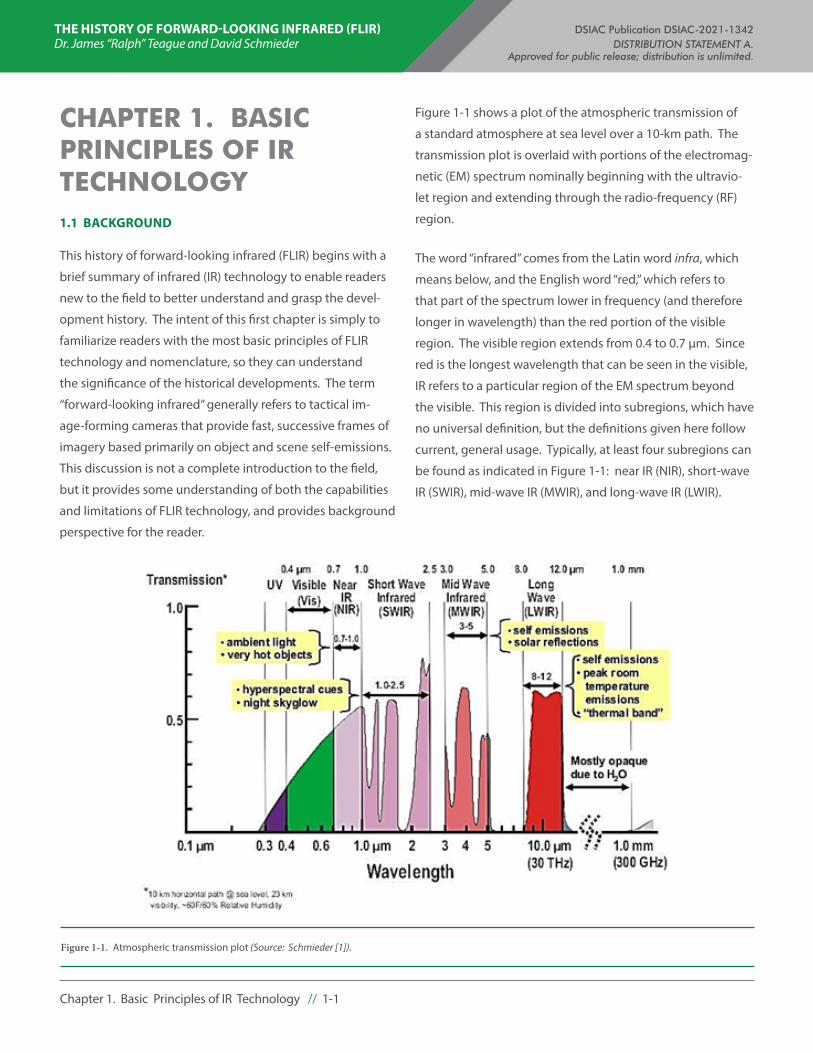
Figure 1-1 shows a plot of the atmospheric transmission of
a standard atmosphere at sea level over a 10-km path. The
transmission plot is overlaid with portions of the electromag-
netic (EM) spectrum nominally beginning with the ultravio-
let region and extending through the radio-frequency (RF)
region.
The word “infrared” comes from the Latin word infra, which
means below, and the English word “red,” which refers to
that part of the spectrum lower in frequency (and therefore
longer in wavelength) than the red portion of the visible
region. The visible region extends from 0.4 to 0.7 µm. Since
red is the longest wavelength that can be seen in the visible,
IR refers to a particular region of the EM spectrum beyond
the visible. This region is divided into subregions, which have
no universal definition, but the definitions given here follow
current, general usage. Typically, at least four subregions can
be found as indicated in Figure 1-1: near IR (NIR), short-wave
IR (SWIR), mid-wave IR (MWIR), and long-wave IR (LWIR).
Figure 1-1. Atmospheric transmission plot (Source: Schmieder [1]).
THE HISTORY OF FORWARD-LOOKING INFRARED (FLIR) DSIAC Publication DSIAC-2021-1342 Dr. James “Ralph” Teague and David Schmieder DISTRIBUTION STATEMENT A. Approved for public release; distribution is unlimited.
Chapter 1. Basic Principles of IR Technology // 1-2
Generally, the subregions are defined by the existence of a
useful atmospheric transmission “window.” These windows,
however, are sometimes subdivided according to detector re-
sponse capabilities. For instance, most recent nomenclature
defines NIR as nominally the 0.7–1.0-µm region in accordance
with the response of silicon detectors (but without the visible
band response of silicon detectors) and night vision goggles
(0.6–0.9 µm). SWIR (1.0–2.5 µm) had not been widely used
before the advent of hyperspectral imaging (HSI) systems.
Early HSI favored that region for day target discrimination.
Now, night ambient light-amplifying sensors exploit that
region as well and use the higher-ambient illumination avail-
able from night skyglow.
The MWIR and LWIR regions dominate current tactical mili-
tary IR applications. The MWIR region, nominally 3.0–5.0 µm,
and the LWIR 8–12-µm region are defined only by windows in
the atmosphere. Beyond 12 µm there is a large gap between
where the LWIR band ends and where the near millimeter
wave RF band begins. The gap is due to a severe atmospheric
absorption “wall” region that extends out to and helps define
the beginning of the RF band. For tactical applications within
the Earth’s atmosphere, the IR community considers the “IR”
spectral region to extend roughly from 0.7 µm, where the
visible band ends, to about 14 µm, where the atmospheric
absorption wall begins. For extraterrestrial space applica-
tions where atmospheric windows don’t apply, the definition
of the IR spectral region readily extends out to almost 30 µm,
and the region between 14 and 30 µm is called the very long-
wave IR (VLWIR).
1.2 SOURCES OF IR RADIATION
Sources of IR radiation ultimately define the application do-
main for IR technology; those sources are generally anything
that produces heat. Fortunately, for the usefulness of IR
technology, that includes almost everything. For instance,
most people know from personal experience that hot objects
radiate heat because they can feel it, but they can’t see that
object’s self-emissions unless it is very hot like a fireplace
poker. Therefore, it is less obvious that objects at room
temperature also emit radiation because those objects are in
radiative equilibrium with their observer, and there is no net
radiation transfer. If that person stood next to a cold exterior
window inside a warm enclosure on a cold day, they would
readily feel the unequal exchange. Nevertheless, radiative
nonequilibrium is not a requirement for being able to detect
IR radiation. It is only required that objects have an apparent
temperature difference from their background. The tempera-
ture difference can be the result of either temperature and/
or emissivity differences. Objects need only to emit slightly
more or less than their immediate backgrounds to be detect-
able. For example, even the “first generation” of IR imagers
could easily sense a 0.1°C apparent temperature difference.
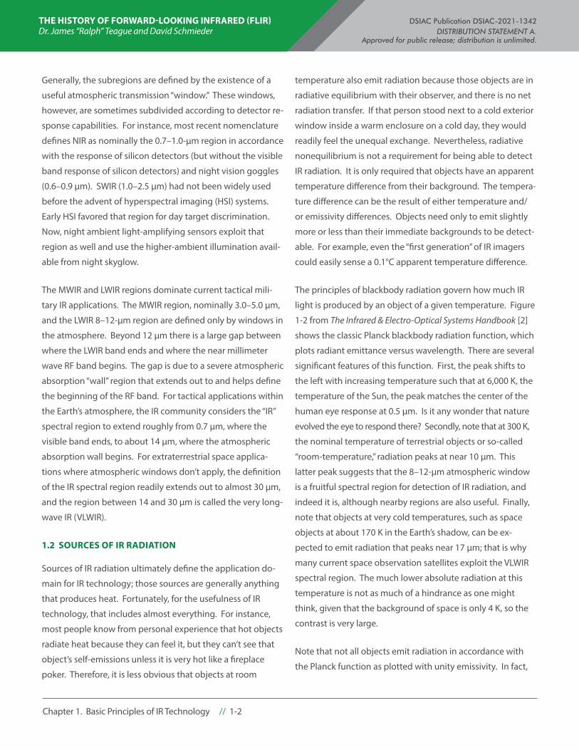
The principles of blackbody radiation govern how much IR
light is produced by an object of a given temperature. Figure
1-2 from The Infrared & Electro-Optical Systems Handbook [2]
shows the classic Planck blackbody radiation function, which
plots radiant emittance versus wavelength. There are several
significant features of this function. First, the peak shifts to
the left with increasing temperature such that at 6,000 K, the
temperature of the Sun, the peak matches the center of the
human eye response at 0.5 µm. Is it any wonder that nature
evolved the eye to respond there? Secondly, note that at 300 K,
the nominal temperature of terrestrial objects or so-called
“room-temperature,” radiation peaks at near 10 µm. This
latter peak suggests that the 8–12-µm atmospheric window
is a fruitful spectral region for detection of IR radiation, and
indeed it is, although nearby regions are also useful. Finally,
note that objects at very cold temperatures, such as space
objects at about 170 K in the Earth’s shadow, can be ex-
pected to emit radiation that peaks near 17 µm; that is why
many current space observation satellites exploit the VLWIR
spectral region. The much lower absolute radiation at this
temperature is not as much of a hindrance as one might
think, given that the background of space is only 4 K, so the
contrast is very large.
Note that not all objects emit radiation in accordance with
the Planck function as plotted with unity emissivity. In fact,
THE HISTORY OF FORWARD-LOOKING INFRARED (FLIR) DSIAC Publication DSIAC-2021-1342 Dr. James “Ralph” Teague and David Schmieder DISTRIBUTION STATEMENT A. Approved for public release; distribution is unlimited.
Chapter 1. Basic Principles of IR Technology // 1-3
virtually none of them do. For instance, actual emission
spectra depend upon the shape of an object’s spectral emis-
sivity characteristics and that shape is seldom that of a pure
blackbody. In fact, an object’s emissivity is a strong func-
tion of its material properties and not only seldom reaches
unity but varies considerably with wavelength. Hence, most
objects are called “selective radiators” whose emissions are
strongly dependent on the spectral shape of their emissivity.
If an object does happen to have a shape close to that of a
blackbody, it almost always has less than unity emissivity, and
is referred to as a “graybody.” Hence, the terms blackbody and
graybody are idealizations.
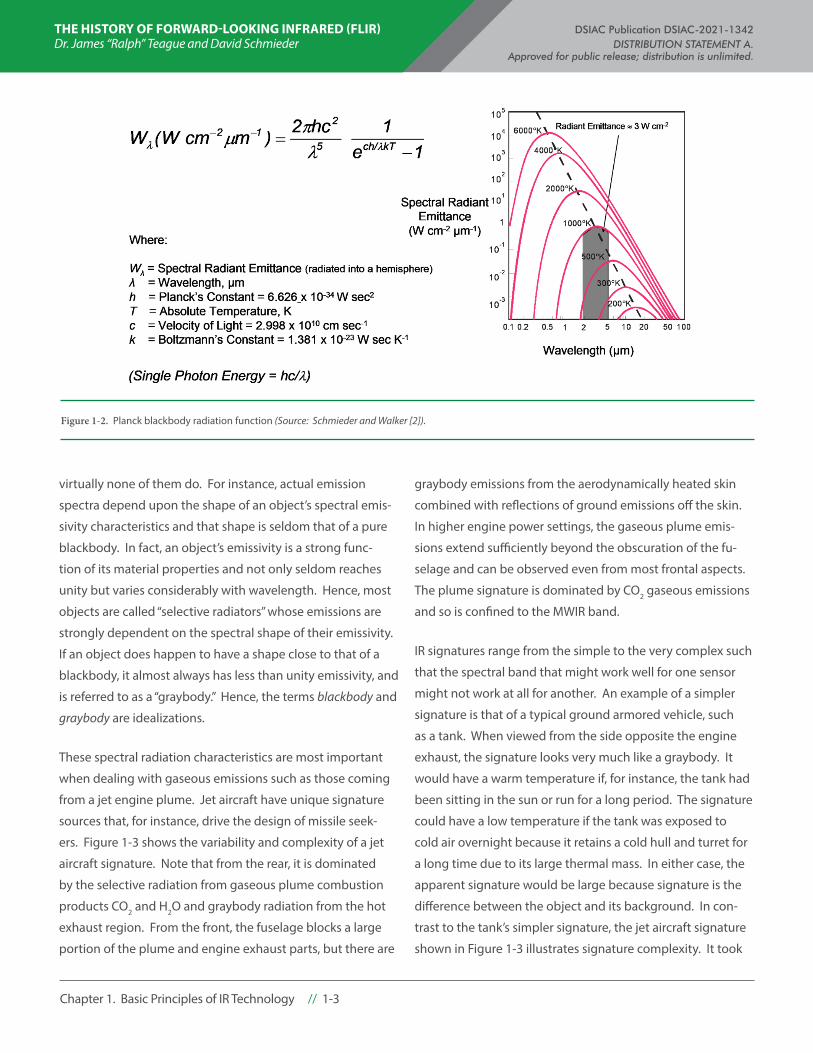
These spectral radiation characteristics are most important
when dealing with gaseous emissions such as those coming
from a jet engine plume. Jet aircraft have unique signature
sources that, for instance, drive the design of missile seek-
ers. Figure 1-3 shows the variability and complexity of a jet
aircraft signature. Note that from the rear, it is dominated
by the selective radiation from gaseous plume combustion
products CO2 and H2O and graybody radiation from the hot
exhaust region. From the front, the fuselage blocks a large
portion of the plume and engine exhaust parts, but there are
graybody emissions from the aerodynamically heated skin
combined with reflections of ground emissions off the skin.
In higher engine power settings, the gaseous plume emis-
sions extend sufficiently beyond the obscuration of the fu-
selage and can be observed even from most frontal aspects.
The plume signature is dominated by CO2 gaseous emissions
and so is confined to the MWIR band.
IR signatures range from the simple to the very complex such
that the spectral band that might work well for one sensor
might not work at all for another. An example of a simpler
signature is that of a typical ground armored vehicle, such
as a tank. When viewed from the side opposite the engine
exhaust, the signature looks very much like a graybody. It
would have a warm temperature if, for instance, the tank had
been sitting in the sun or run for a long period. The signature
could have a low temperature if the tank was exposed to
cold air overnight because it retains a cold hull and turret for
a long time due to its large thermal mass. In either case, the
apparent signature would be large because signature is the
difference between the object and its background. In con-
trast to the tank’s simpler signature, the jet aircraft signature
shown in Figure 1-3 illustrates signature complexity. It took
Figure 1-2. Planck blackbody radiation function (Source: Schmieder and Walker [2]).
THE HISTORY OF FORWARD-LOOKING INFRARED (FLIR) DSIAC Publication DSIAC-2021-1342 Dr. James “Ralph” Teague and David Schmieder DISTRIBUTION STATEMENT A. Approved for public release; distribution is unlimited.
Chapter 1. Basic Principles of IR Technology // 1-4
many decades after IR detectors were developed for design-
ers to fully appreciate the challenges facing IR technology
due to both the variability and the complexity of signatures.
1.3 IR DETECTORS
Of course, there would be no IR technology if it were not for
the development of IR detectors. This book will describe the
fascinating process of insight and luck that led to the devel-
opment of modern detectors. For now, a summary of only
the most general types will provide the background needed
to appreciate the history that follows.
There are two very broad categories of detectors: thermal
and quantum. Thermal detectors are essentially miniature
thermometers that detect radiation from the heat that
objects generate when absorbing light. Quantum detectors
are based on semiconductors, which absorb photons at
the subatomic level and cause electrons to be raised from
the valence band to the conduction band where they can
be detected as a current or voltage change. Both detector
types are widely used in modern FLIRs. The main type of
thermal detector is a bolometer, which changes resistance
with a change in temperature. That resistance change is then
sensed by passing a current through it. Although thermal
detectors are inexpensive and can be operated at room tem-
perature, they typically have a slow response time. Quantum
detectors require a cryocooler to operate below 200 K but are
more sensitive and have a faster response time than thermal
detectors.
Quantum detectors can be further divided into at least three
types: photoconductive (PC), photovoltaic (PV), and photo-
emissive. PC detectors operate by developing a change in
resistance in proportion to the amount of incident light. Like
bolometers, the resistance change is detected by passing a
current through it. PV detectors, however, have a p-n junc-
tion like roof-top solar cells and can generate either a current
or a voltage from their conversion of photons into photo-
electrons. Photoemissive detectors operate by ejecting an
electron from their surface when a photon is absorbed. The
photons are accelerated by an electric field and are con-
verted into visible light when they impinge on a phosphor
screen.
Figure 1-3. A representative jet aircraft signature illustrates the varied contributions from both skin self-emissions and ground emission reflections and also the dominant contributions from the plume and hot exhaust parts when viewed from the rear (Source: General Dynamics).
THE HISTORY OF FORWARD-LOOKING INFRARED (FLIR) DSIAC Publication DSIAC-2021-1342 Dr. James “Ralph” Teague and David Schmieder DISTRIBUTION STATEMENT A. Approved for public release; distribution is unlimited.
Chapter 1. Basic Principles of IR Technology // 1-5
Although the more common detector types are PC, PV,
photoemissive (quantum detectors), and bolometric thermal
detectors, there are other sensing mechanisms. However,
knowledge of these common types is helpful in understand-
ing the history of IR development.
1.3.1 Examples of IR Systems
IR imaging systems include targeting systems (FLIRs) (Fig-
ures 1-4 and 1-5), surveillance systems designed for either
warning or intelligence gathering (Figure 1-6), or IR search
and track (IRST) systems, used mostly on ships and aircraft
(Figure 1-7) for both detection and tracking functions. FLIRs
are most commonly used for target detection and identifica-
tion—a process called “target acquisition.” They then serve
as fire-control systems that keep a crosshair on the target for
engagement with options that include gun fire, laser des-
ignation for missile homing, or handoff to other IR homing
seekers. Surveillance, warning, and IRST systems often form
images like FLIRs do, but differ, albeit sometimes only slightly,
by mission application. For instance, surveillance systems are
IR cameras used specifically for reconnaissance and intelli-
gence gathering. Warning systems are used to detect threat
missile launches, and IRSTs are cameras with a large field-of-
Figure 1-4. Sniper targeting pod (Source: U.S. Air Force photo/Senior Airman Noah Johnson).
Figure 1-5. Apache attack helicopter Modern Target Acquisition and Des-ignation Sight (MTADS) targeting system (Source: U.S. Army Photo/Brigitte Rodriguez).
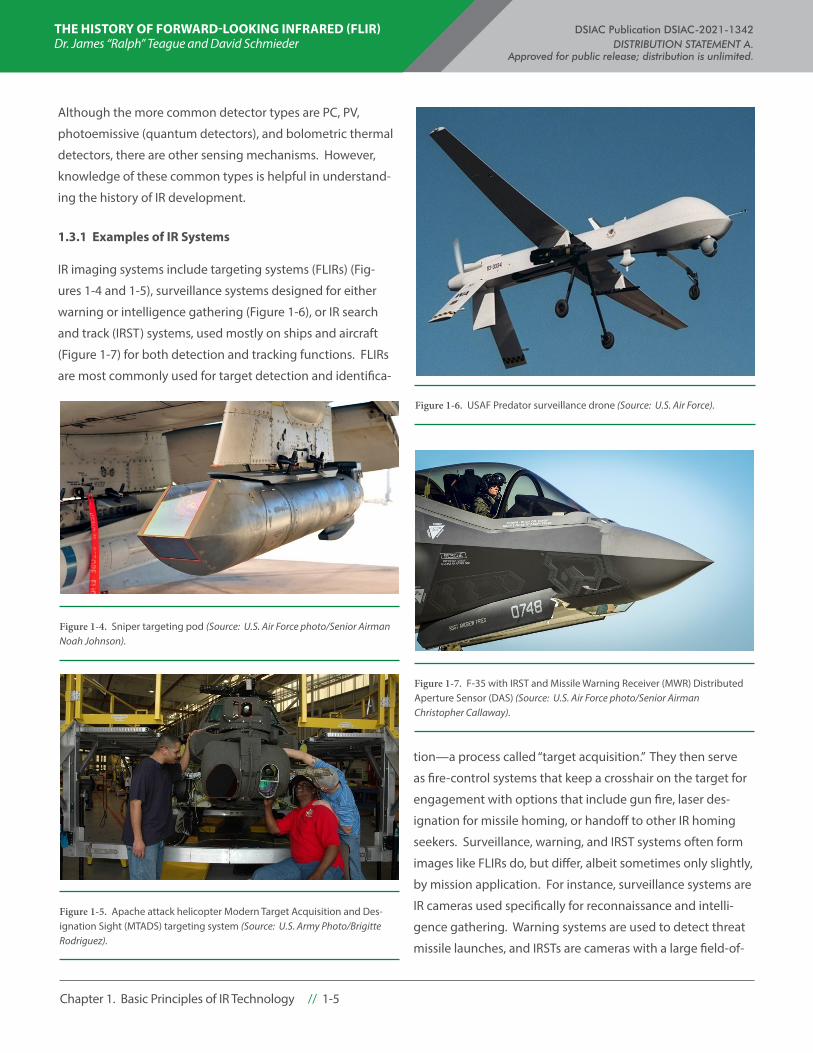
Figure 1-6. USAF Predator surveillance drone (Source: U.S. Air Force).
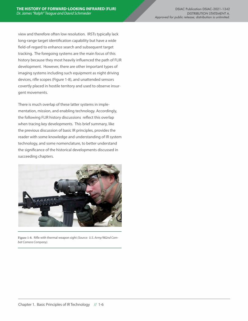
Figure 1-7. F-35 with IRST and Missile Warning Receiver (MWR) Distributed Aperture Sensor (DAS) (Source: U.S. Air Force photo/Senior Airman Christopher Callaway).
THE HISTORY OF FORWARD-LOOKING INFRARED (FLIR) DSIAC Publication DSIAC-2021-1342 Dr. James “Ralph” Teague and David Schmieder DISTRIBUTION STATEMENT A. Approved for public release; distribution is unlimited.
Chapter 1. Basic Principles of IR Technology // 1-6
view and therefore often low resolution. IRSTs typically lack
long-range target identification capability but have a wide
field-of-regard to enhance search and subsequent target
tracking. The foregoing systems are the main focus of this
history because they most heavily influenced the path of FLIR
development. However, there are other important types of
imaging systems including such equipment as night driving
devices, rifle scopes (Figure 1-8), and unattended sensors
covertly placed in hostile territory and used to observe insur-
gent movements.
There is much overlap of these latter systems in imple-
mentation, mission, and enabling technology. Accordingly,
the following FLIR history discussions reflect this overlap
when tracing key developments. This brief summary, like
the previous discussion of basic IR principles, provides the
reader with some knowledge and understanding of IR system
technology, and some nomenclature, to better understand
the significance of the historical developments discussed in
succeeding chapters.
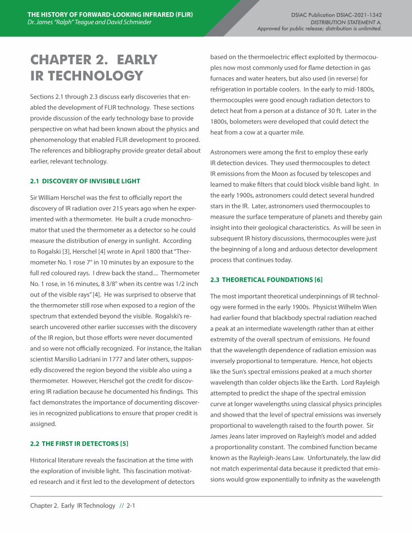
Figure 1-8. Rifle with thermal weapon sight (Source: U.S. Army/982nd Com-bat Camera Company).
THE HISTORY OF FORWARD-LOOKING INFRARED (FLIR) DSIAC Publication DSIAC-2021-1342 Dr. James “Ralph” Teague and David Schmieder DISTRIBUTION STATEMENT A. Approved for public release; distribution is unlimited.
Chapter 2. Early IR Technology // 2-1
CHAPTER 2. EARLY IR TECHNOLOGY Sections 2.1 through 2.3 discuss early discoveries that en-
abled the development of FLIR technology. These sections
provide discussion of the early technology base to provide
perspective on what had been known about the physics and
phenomenology that enabled FLIR development to proceed.
The references and bibliography provide greater detail about
earlier, relevant technology.
2.1 DISCOVERY OF INVISIBLE LIGHT
Sir William Herschel was the first to officially report the
discovery of IR radiation over 215 years ago when he exper-
imented with a thermometer. He built a crude monochro-
mator that used the thermometer as a detector so he could
measure the distribution of energy in sunlight. According
to Rogalski [3], Herschel [4] wrote in April 1800 that “Ther-
mometer No. 1 rose 7° in 10 minutes by an exposure to the
full red coloured rays. I drew back the stand.... Thermometer
No. 1 rose, in 16 minutes, 8 3/8° when its centre was 1/2 inch
out of the visible rays” [4]. He was surprised to observe that
the thermometer still rose when exposed to a region of the
spectrum that extended beyond the visible. Rogalski’s re-
search uncovered other earlier successes with the discovery
of the IR region, but those efforts were never documented
and so were not officially recognized. For instance, the Italian
scientist Marsilio Ladriani in 1777 and later others, suppos-
edly discovered the region beyond the visible also using a
thermometer. However, Herschel got the credit for discov-
ering IR radiation because he documented his findings. This
fact demonstrates the importance of documenting discover-
ies in recognized publications to ensure that proper credit is
assigned.
2.2 THE FIRST IR DETECTORS [5]
Historical literature reveals the fascination at the time with
the exploration of invisible light. This fascination motivat-
ed research and it first led to the development of detectors
based on the thermoelectric effect exploited by thermocou-
ples now most commonly used for flame detection in gas
furnaces and water heaters, but also used (in reverse) for
refrigeration in portable coolers. In the early to mid-1800s,
thermocouples were good enough radiation detectors to
detect heat from a person at a distance of 30 ft. Later in the
1800s, bolometers were developed that could detect the
heat from a cow at a quarter mile.
Astronomers were among the first to employ these early
IR detection devices. They used thermocouples to detect
IR emissions from the Moon as focused by telescopes and
learned to make filters that could block visible band light. In
the early 1900s, astronomers could detect several hundred
stars in the IR. Later, astronomers used thermocouples to
measure the surface temperature of planets and thereby gain
insight into their geological characteristics. As will be seen in
subsequent IR history discussions, thermocouples were just
the beginning of a long and arduous detector development
process that continues today.
2.3 THEORETICAL FOUNDATIONS [6]
The most important theoretical underpinnings of IR technol-
ogy were formed in the early 1900s. Physicist Wilhelm Wien
had earlier found that blackbody spectral radiation reached
a peak at an intermediate wavelength rather than at either
extremity of the overall spectrum of emissions. He found
that the wavelength dependence of radiation emission was
inversely proportional to temperature. Hence, hot objects
like the Sun’s spectral emissions peaked at a much shorter
wavelength than colder objects like the Earth. Lord Rayleigh
attempted to predict the shape of the spectral emission
curve at longer wavelengths using classical physics principles
and showed that the level of spectral emissions was inversely
proportional to wavelength raised to the fourth power. Sir
James Jeans later improved on Rayleigh’s model and added
a proportionality constant. The combined function became
known as the Rayleigh-Jeans Law. Unfortunately, the law did
not match experimental data because it predicted that emis-
sions would grow exponentially to infinity as the wavelength
THE HISTORY OF FORWARD-LOOKING INFRARED (FLIR) DSIAC Publication DSIAC-2021-1342 Dr. James “Ralph” Teague and David Schmieder DISTRIBUTION STATEMENT A. Approved for public release; distribution is unlimited.
Chapter 2. Early IR Technology // 2-2
got shorter. Of course, the law not only failed to match mea-
surements, it was physically impossible and became known
as the UV catastrophe. The solution remained a puzzling
mystery until Max Plank found the explanation.
Plank’s breakthrough that explained the flaw in the Rayleigh-
Jeans Law was his epiphany that energy could only be emit-
ted in quantized form. As a result of this breakthrough, Plank
concluded that no energy could be emitted until its energy
was large enough to escape. Since the quanta at lower wave-
lengths contained higher energy, they could not be emitted
in larger quantities until the temperature increased. There-
fore, the number of quanta emitted at any given temperature
would be limited, and the energy dependence on wave-
length forced the blackbody spectral radiation curve lower as
wavelength decreased.
Plank’s discovery arguably helped Albert Einstein to further
conclude that light must be quantized as well. This conclu-
sion led him to explain the photoelectric effect, which posits
that light quanta (later called photons) of sufficient energy
can force electrons to be emitted from a material’s surface
into free space. Einstein proposed this explanation knowing
that it was not the rate of photons impinging on a materi-
al’s surface that made this happen but, instead, it was the
wavelength because ejection could happen even if the rate
were low. It was later seen that these quanta raise valence
electrons to the conduction band inside a material, and this
also became known as a manifestation of the photoelectric
effect. The photoelectric effect is the basic underlying princi-
ple for how modern IR quantum detectors work. Einstein was
awarded a Nobel Prize for discovering it.
The remaining chapters discuss how the application of these
fundamental discoveries led to the invention of IR sensors
and ultimately to the development of modern FLIRs.

THE HISTORY OF FORWARD-LOOKING INFRARED (FLIR) DSIAC Publication DSIAC-2021-1342 Dr. James “Ralph” Teague and David Schmieder DISTRIBUTION STATEMENT A. Approved for public release; distribution is unlimited.
Chapter 3. Early Military IR Use in World Wars I and II // 3-1
CHAPTER 3. EARLY MILITARY IR USE IN WORLD WARS I AND II3.1 BACKGROUND
Interest in IR technology prior to about 1910 was widely
dispersed, and development was sporadic and haphazard
until its potential military applications were recognized. Barr
and Arnquist [6, 7] found that research programs established
during World War I (WWI) focused first on covert communica-
tion devices that led to field evaluations, but apparently little
deployment. However, according to Hudson [8], the period
between 1910 and 1920, thus overlapping WWI, was rich with
patent disclosures that exploited IR for object detection to
include aircraft, ships, personnel, artillery, and even icebergs.
Hudson reported that patents during that period included
communications equipment, but also disclosed other militar-
ily useful devices for intrusion detection and “the guidance
of aerial torpedoes” or what we now call guided missiles. The
more germane predecessor to today’s IR applications was the
IRST, which was developed by the British during WWI, though
it was not called that at the time. According to Hudson, these
early systems could detect aircraft out to about a mile. Mili-
tary IR research and development were firmly entrenched by
the end of WWI. However, it was not until World War II (WWII)
and events shortly thereafter that progress was sufficient to
lay the groundwork for what is today’s modern IR technology.
3.2 EARLY DETECTORS (PHOTOCONDUCTIVE,
PHOTOVOLTAIC, PHOTOEMISSIVE, BOLOMETRIC)
IR technology begins with the development of suitable
detectors. The principles of three of the four main detector
types were in place by WWI: photoconductive, photovoltaic,
and bolometric. (The fourth type was photoemissive.) As
discussed in Section 1.3, in response to incident photons that
raise electrons to the conduction band in quantum detectors,
photoconductors sense a change of resistance; photovoltaic
detectors sense a change in voltage or current across a p-n
junction; and bolometric thermal detectors sense a change
in resistance to electric current when the incident photons
change their temperature (as do other unintentional sources
of heat). Smith reported the first discovery of photocon-
ductivity in an 1873 paper in Nature [9], although detectors
using the principle were not invented until much later [7, 9].
Bose patented the first IR photovoltaic detector in 1904 using
naturally occurring lead sulfide (PbS) [8, 10]. Although pho-
toconductivity and the IR photovoltaic detector would later
be viewed as major discoveries, they were largely ignored at
the time.
The first practical detectors began with the discovery of
bolometers [7, 10]. Bolometric detectors were invented by
famed astronomer Samuel P. Langley in 1878 [6]. Langley
was able to detect the heat from a cow at the impressive
distance of a quarter mile. He used his bolometer to discov-
er new atomic and molecular absorption lines in the IR and
attempted to measure the temperature of the Moon with it.
All three of these detector types (photoconductive, photo-
voltaic, and bolometric) now play a key role in the modern
application of IR technology.
The other major detector type, photoemissive, was not
discovered until shortly after WWI. Recall that photoemissive
detectors directly exploit the photoelectric effect by detect-
ing electrons externally ejected by special photocathode
materials. Their discovery was the basis for image intensifiers,
which amplified ambient light first in the visible and, later, in
the near IR, but only out to about 1.3 µm. The photoemissive
detector was discovered in the U.S. in the 1920s and had an
impact in WWII when the Germans deployed it early in the
war. Ironically, the U.S. finally did so in the Pacific just as the
war was about to end.
3.3 IR SYSTEMS IN WWI
The military first showed interest in IR devices during WWI
when it became apparent that invisible light from IR signal-
ing devices could be useful. However, these devices did not
appear to get much attention for what was arguably later
THE HISTORY OF FORWARD-LOOKING INFRARED (FLIR) DSIAC Publication DSIAC-2021-1342 Dr. James “Ralph” Teague and David Schmieder DISTRIBUTION STATEMENT A. Approved for public release; distribution is unlimited.
Chapter 3. Early Military IR Use in World Wars I and II // 3-2
thought of as the Holy Grail of IR, i.e., seeing in the dark.
Signal communication was the first military application of
IR in the U.S. according to Arnquist [7]. This application was
enabled when T. W. Case invented the photoconductive de-
tector in 1917 from thallous sulfide (TI2S) [11]. It was used to
demonstrate a covert blinking communication device for the
U.S. military that could transmit and receive at an effective
two-way range of 18 miles [7] and later to also transmit voice
signals. This detector was subsequently used in the field to
covertly help guide planes to landing strips and to guide ship
convoys.
The successful use of TI2S detectors also apparently stimu-
lated foreign interest in the IR and motivated Russia, Italy,
and England to develop similar detectors from this material
after the war. The Germans, who were to later lead the world
in photoconductive detector development, apparently only
looked at selenium photoconductors [7] for visible commu-
nications during this period. Rogalski [12] claimed the British
developed the first, what must have been fledgling, IRST in
1914 using a bolometer. While little information is available,
this IRST could well have been the first attempt to use IR to
see objects in the dark.
Shortly after the war, in the U.S., General Electric (GE) report-
edly [13] also built an experimental aircraft detection device
that could locate a light bomber at a range of 22 miles. How-
ever, most IR efforts languished because radar was seen as
the more promising sensor technology. Although seeming
to make little headway in WWI, the development of IR tech-
nology for military applications was firmly established.
3.4 LEAD UP TO AND USE OF IR SYSTEMS IN WWII
D. J. Lovell of The University of Michigan provided a notewor-
thy summary of U.S. IR technology development from just
prior to WWII to the postwar period [14]. The U.S. Air Force
Office of Scientific Research had the foresight to fund Lovell’s
historical account of IR technology development in 1968
before it was forever lost. Lovell’s account has the distinction
of resulting from numerous personal interviews with such
key players in the U.S. as Robert Cashman and Henry Levin-
stein, and from Germany, Edgar Kutzscher. This distinction,
he observed, provided a broader understanding than would
otherwise have been possible from merely reading the archi-
val literature. He also pointed out the importance of what
was to later become a hallmark of progress in U.S. IR tech-
nology development, i.e., “the curious stimulus afforded by
the inter-communication of results” among often competing
interests. These communications were fostered by classified
symposia (the Infrared Information Symposium [IRIS] and
later the Military Sensing Symposium [MSS]), which would
become key sources of IR information dissemination.
While Lovell’s interviews were important, not to be mini-
mized is Arnquist’s IR history survey [7] published in a 1959
Institute of Radio Engineers (IRE) proceedings, which was
based on papers found in the archival literature. The remain-
der of this chapter is largely an abridged collection of obser-
vations taken from both Lovell’s and Arnquist’s research.
3.4.1 German IR Research Program
Germany resumed its military IR program in about 1932. It
exploited PbS first in natural crystal form and later as chemi-
cally deposited photoconductors. Shortly thereafter, Ger-
man scientists discovered that lead selenide (PbSe) also had
favorable detector qualities. During this period, they found
that cooling either by using solid carbon dioxide (195 K) or
liquid nitrogen (LN2) (77 K) would improve IR detection sensi-
tivity and incorporated those cooling methods into devices.
Bolometers were also developed, which enabled Germany to
build ground sensors for detecting aircraft and ships. Aircraft
sensors were developed to direct searchlights for anti-aircraft
fire. Airborne versions were also used to develop air-to-air
“IRSTs” for night fighters, and both air-to-air and air-to-
ground missile seekers (although no missiles) were ultimately
mass produced with those capabilities. According to John-
son [15], near the end of the war, some PbS systems were also
used along coastlines to detect ships and aircraft.
THE HISTORY OF FORWARD-LOOKING INFRARED (FLIR) DSIAC Publication DSIAC-2021-1342 Dr. James “Ralph” Teague and David Schmieder DISTRIBUTION STATEMENT A. Approved for public release; distribution is unlimited.
Chapter 3. Early Military IR Use in World Wars I and II // 3-3
Kiel IV and PbS Detector Development. Only a few IRSTs
were built, but the scanning Kiel IV night fighter system using
PbS almost made it into production before the war ended.
By 1944, 1,000 PbS cells were being produced annually [16].
The Kiel IV was developed by Kutzscher’s group at a company
in the city of Kiel. It used PbS photoconductors perfected
by Kutzscher while at the University of Berlin. Unfortunately,
Kiel was in that part of Germany later occupied by Russia,
and so the Russians were the beneficiaries of equipment,
data, and reports owned by Kutzscher’s group. This situation
gave Russia a boost in IR development that benefitted them
throughout the Cold War that followed. However, Kutzscher
and several of his colleagues escaped to the West and
arguably gave the U.S. an even greater windfall of expertise.
This contribution contrasts with the rather slow progress in
U.S. photoconductor development during the war. Robert
Cashman at Northwestern University began work with TI2S
films in 1941 and, in 1944, he considered PbS but did not
fully embrace it until he and others found out about German
progress after the war.
German PbS detector developments prior to and during
WWII were based largely on empirical studies and fabrication
trial and error rather than on theoretical insight since basic
semiconductor theory was not well understood. Accordingly,
recipes were developed experimentally, and key processes
became more of an art than a science. (Some would say
detector material understanding is still more art than science
as of this writing.) Many groups were involved including
university laboratories and private companies. Nevertheless,
Lovell claims that productive interchange was maintained
among all groups through organized meetings and pub-
lished proceedings. This interchange and sharing of empiri-
cal data accelerated progress, thus partly mitigating the lack
of a guiding theoretical understanding of semiconductors.
It was fortuitous for the Germans that they did not spend
much time trying to understand the physics of PbS detector
material since they are not yet well understood. Various or-
ganizations in the U.S. have only recently (circa 2010) started
to reexamine PbS because of the promise the material holds
for high-operating-temperature, low-cost applications such
as for missile-launch warning receivers.
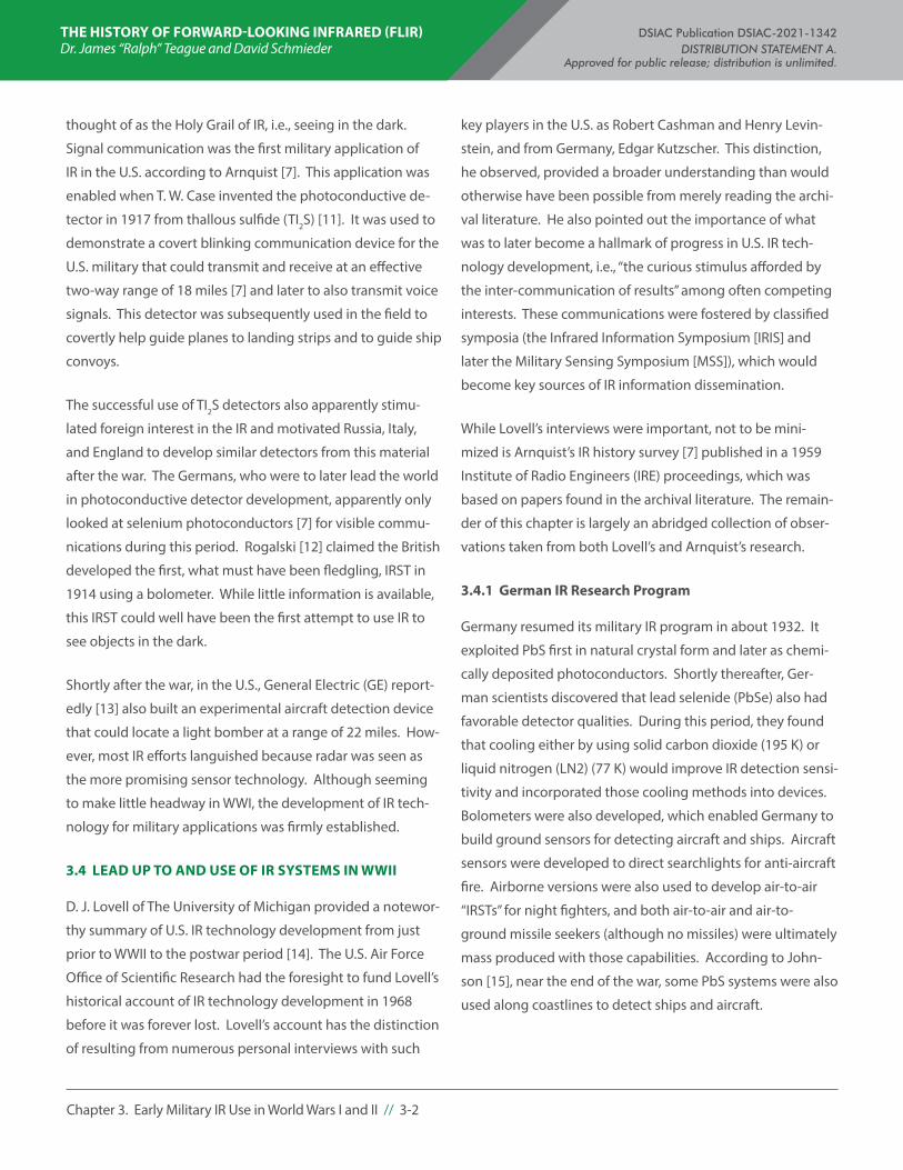
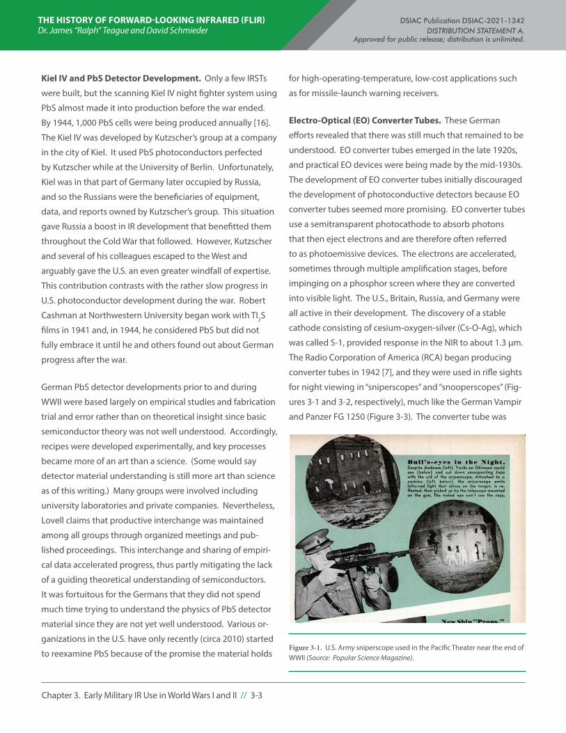
Electro-Optical (EO) Converter Tubes. These German
efforts revealed that there was still much that remained to be
understood. EO converter tubes emerged in the late 1920s,
and practical EO devices were being made by the mid-1930s.
The development of EO converter tubes initially discouraged
the development of photoconductive detectors because EO
converter tubes seemed more promising. EO converter tubes
use a semitransparent photocathode to absorb photons
that then eject electrons and are therefore often referred
to as photoemissive devices. The electrons are accelerated,
sometimes through multiple amplification stages, before
impinging on a phosphor screen where they are converted
into visible light. The U.S., Britain, Russia, and Germany were
all active in their development. The discovery of a stable
cathode consisting of cesium-oxygen-silver (Cs-O-Ag), which
was called S-1, provided response in the NIR to about 1.3 µm.
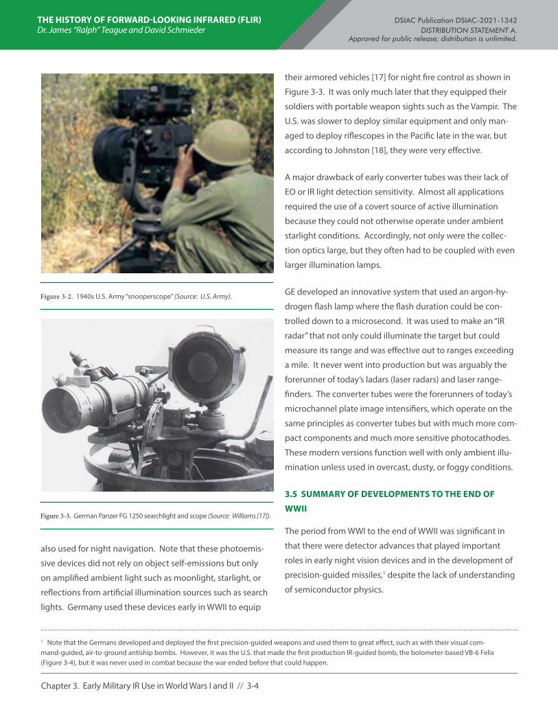
The Radio Corporation of America (RCA) began producing
converter tubes in 1942 [7], and they were used in rifle sights
for night viewing in “sniperscopes” and “snooperscopes” (Fig-
ures 3-1 and 3-2, respectively), much like the German Vampir
and Panzer FG 1250 (Figure 3-3). The converter tube was
Figure 3-1. U.S. Army sniperscope used in the Pacific Theater near the end of WWII (Source: Popular Science Magazine).
THE HISTORY OF FORWARD-LOOKING INFRARED (FLIR) DSIAC Publication DSIAC-2021-1342 Dr. James “Ralph” Teague and David Schmieder DISTRIBUTION STATEMENT A. Approved for public release; distribution is unlimited.
Chapter 3. Early Military IR Use in World Wars I and II // 3-4
also used for night navigation. Note that these photoemis-
sive devices did not rely on object self-emissions but only
on amplified ambient light such as moonlight, starlight, or
reflections from artificial illumination sources such as search
lights. Germany used these devices early in WWII to equip
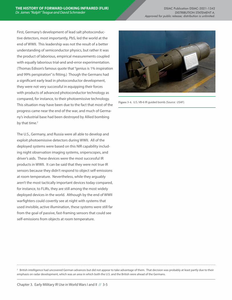
1 Note that the Germans developed and deployed the first precision-guided weapons and used them to great effect, such as with their visual com-mand-guided, air-to-ground antiship bombs. However, it was the U.S. that made the first production IR-guided bomb, the bolometer-based VB-6 Felix (Figure 3-4), but it was never used in combat because the war ended before that could happen.
their armored vehicles [17] for night fire control as shown in
Figure 3-3. It was only much later that they equipped their
soldiers with portable weapon sights such as the Vampir. The
U.S. was slower to deploy similar equipment and only man-
aged to deploy riflescopes in the Pacific late in the war, but
according to Johnston [18], they were very effective.
A major drawback of early converter tubes was their lack of
EO or IR light detection sensitivity. Almost all applications
required the use of a covert source of active illumination
because they could not otherwise operate under ambient
starlight conditions. Accordingly, not only were the collec-
tion optics large, but they often had to be coupled with even
larger illumination lamps.
GE developed an innovative system that used an argon-hy-
drogen flash lamp where the flash duration could be con-
trolled down to a microsecond. It was used to make an “IR
radar” that not only could illuminate the target but could
measure its range and was effective out to ranges exceeding
a mile. It never went into production but was arguably the
forerunner of today’s ladars (laser radars) and laser range-
finders. The converter tubes were the forerunners of today’s
microchannel plate image intensifiers, which operate on the
same principles as converter tubes but with much more com-
pact components and much more sensitive photocathodes.
These modern versions function well with only ambient illu-
mination unless used in overcast, dusty, or foggy conditions.
3.5 SUMMARY OF DEVELOPMENTS TO THE END OF
WWII
The period from WWI to the end of WWII was significant in
that there were detector advances that played important
roles in early night vision devices and in the development of
precision-guided missiles,1 despite the lack of understanding
of semiconductor physics.
Figure 3-2. 1940s U.S. Army “snooperscope” (Source: U.S. Army).
Figure 3-3. German Panzer FG 1250 searchlight and scope (Source: Williams [17]).
THE HISTORY OF FORWARD-LOOKING INFRARED (FLIR) DSIAC Publication DSIAC-2021-1342 Dr. James “Ralph” Teague and David Schmieder DISTRIBUTION STATEMENT A. Approved for public release; distribution is unlimited.
Chapter 3. Early Military IR Use in World Wars I and II // 3-5
First, Germany’s development of lead salt photoconduc-
tive detectors, most importantly, PbS, led the world at the
end of WWII. This leadership was not the result of a better
understanding of semiconductor physics, but rather it was
the product of laborious, empirical measurements coupled
with equally laborious trial-and and-error experimentation.
(Thomas Edison’s famous quote that “genius is 1% inspiration
and 99% perspiration” is fitting.) Though the Germans had
a significant early lead in photoconductor development,
they were not very successful in equipping their forces
with products of advanced photoconductor technology as
compared, for instance, to their photoemissive technology.
This situation may have been due to the fact that most of the
progress came near the end of the war, and much of Germa-
ny’s industrial base had been destroyed by Allied bombing
by that time.2
The U.S., Germany, and Russia were all able to develop and
exploit photoemissive detectors during WWII. All of the
deployed systems were based on this NIR capability includ-
ing night observation imaging systems, sniperscopes, and
driver’s aids. These devices were the most successful IR
products in WWII. It can be said that they were not true IR
sensors because they didn’t respond to object self-emissions
at room temperature. Nevertheless, while they arguably
aren’t the most tactically important devices today compared,
for instance, to FLIRs, they are still among the most widely
deployed devices in the world. Although by the end of WWII
warfighters could covertly see at night with systems that
used invisible, active illumination, these systems were still far
from the goal of passive, fast-framing sensors that could see
self-emissions from objects at room temperature.
2 British intelligence had uncovered German advances but did not appear to take advantage of them. That decision was probably at least partly due to their emphasis on radar development, which was an area in which both the U.S. and the British were ahead of the Germans.
Figure 3-4. U.S. VB-6 IR guided bomb (Source: USAF).
THE HISTORY OF FORWARD-LOOKING INFRARED (FLIR) DSIAC Publication DSIAC-2021-1342 Dr. James “Ralph” Teague and David Schmieder DISTRIBUTION STATEMENT A. Approved for public release; distribution is unlimited.
Chapter 4. Post-WWII IR Technology // 4-1
CHAPTER 4. POST-WWII IR TECHNOLOGY 4.1 INTRODUCTION3
Post-WWII IR technology was characterized by foundation
building and infrastructure development. It was heavily
influenced by German detector discoveries and the spread-
ing realization that IR technology offered unique advantages
in warfare. The U.S. exploited much of Germany’s knowledge
after the war by offering refuge to their scientists and engi-
neers. This exploitation led to the successful development
of at least one major IR weapon system that gave the U.S.
an initial advantage in the Cold War: the Navy’s Sidewinder
air-to-air missile that used a PbS detector. However, PbS was
not the dominant detector material because of its limited
spectral response and resulting inability to respond in either
the MWIR or the LWIR bands. Therefore, new materials had to
be developed, and a better understanding of semiconductor
physics was needed.
In addition, the beginning of the Cold War led to a new impe-
tus for national defense and greatly increased funding. De-
spite the many new developments, image-forming systems
were still largely improved versions of WWII sniperscopes. It
was not until the Vietnam War (discussed in Chapter 5) that
passive, fast-framing imaging systems capable of viewing
object self-emissions were developed. Nevertheless, a key
technical base was developed including cooled indium
antimonide (InSb) detectors for the MWIR band that led to a
scanning IRST. Additional important developments included
LWIR band detectors made from mercury-doped germanium
(Ge:Hg) and the later breakthrough discovery of the proper-
ties of mercury cadmium telluride (HgCdTe) detector material
(referred to as “MCT” from here on). Thus, the foundation for
fast-framing FLIRs was laid, but their invention came later.
3 Sources used in this chapter include extensively edited and merged excerpts from Robert Sendall [19], Steve Jost [20], and Kirby Taylor [21] in addition to the many references cited throughout the body of the text.
The post-WWII period is notable for at least seven significant
developments affecting IR technology:
• Increased investment in government laboratories and
the industrial base.
• Improved radiometric standards.
• Better means to communicate knowledge and progress.
• Breakthroughs in detector development.
• Development of high-resolution IRST systems thus
enabling capabilities that contributed to the FLIR
technology base.
• Invention of down-looking line scan mappers that
enabled viewing mid-wave and long-wave images.
• Development of performance metrics for imaging systems.
The development of cryocoolers, Dewars capable of 77 K and
28 K operation, and integrated circuits was also significant,
but those developments are beyond the scope of this book.
This history will focus on the former seven listed develop-
ments and each is described in the discussion that follows.
4.2 INCREASED INVESTMENT IN GOVERNMENT
LABORATORIES AND THE INDUSTRIAL BASE
New expertise in IR technology developed quickly in the
post-war years. Greater funding resulted from the emer-
gence of the post-war Soviet Union as a major threat to
the U.S. and its allies. More government laboratories were
formed, but even more reliance was placed on private con-
tractors and university laboratories. The government and
private laboratories in the first decades of the century were
joined by a new operational model in scale and practice.
The new model consisted of funding through research and
development contracts that proliferated in proportion to
increases in military expenditures. Driven by greater funding,
many contractors, universities, and government laboratories
developed greater expertise.

THE HISTORY OF FORWARD-LOOKING INFRARED (FLIR) DSIAC Publication DSIAC-2021-1342 Dr. James “Ralph” Teague and David Schmieder DISTRIBUTION STATEMENT A. Approved for public release; distribution is unlimited.
Chapter 4. Post-WWII IR Technology // 4-2
All three branches of the armed services had organizations
involved in IR technology development. For the Air Force,
much of the development was conducted in the Avionics
Laboratory at Wright-Patterson Air Force Base (AFB). In
the Navy, the Office of Naval Research (ONR) and the Naval
Research Laboratory (NRL) took the lead. In the Army, the
Army Corps of Engineers set up the Engineer Research and
Development Laboratories (ERDL) in 1954 [22], where the
Research and Photometric section began developing per-
sonalized night vision equipment for individual soldiers. This
unit became the Night Vision Laboratory (NVL) and was later
renamed the Night Vision and Electronic Sensors Directorate
(NVESD), most recently reporting to the U.S. Army Research,
Development, and Engineering Command (RDECOM) and
Communications-Electronics Research, Development and
Engineering Center (CERDEC) [23]. ERDL assumed much
of the responsibility for Army IR technology development.
However, their early emphasis was on NIR imagers that am-
plified night ambient light such as image intensifiers and low
light level televisions (LLLTVs), but it also included active laser
pulse-gated TVs. Army emphasis later changed to the more
promising passive systems that could see self-emissions. By
the mid-1970s, given the Army’s large procurement budget
for outfitting its many ground and air vehicles with night
vision equipment, the NVL developed considerable expertise
and arguably became the lead government laboratory influ-
encing the direction of IR technology.
Still, most of the actual IR development was accomplished by
private industry. The major detector firms by the late 1960s
were the Santa Barbara Research Center (SBRC) (a subsidiary
of Hughes Aircraft Corporation [HAC]), Honeywell, and Texas
Instruments (TI). Thus, apart from the University of Michigan,
itself a major beneficiary of military contracts, and Syracuse
University, the bulk of IR research was being conducted by
private firms. Previously centered in universities, IR tech-
nology had been redirected by the Cold War to become a
specialty outside the mainstream of academic science, much
like photometry.
4.3 IMPROVED RADIOMETRIC STANDARDS
New infrastructure was needed to address the problem of ra-
diometric references and measurement standards. The very
notion of a reference standard was problematic due to the
complex nature of real-world object emissions. Similarly, the
nature of aircraft as sources of light is complex. The leading
surfaces of a jet airplane or missile are heated by aerody-
namic friction, and they emit IR light similar to a blackbody
source. Jet and rocket nozzles are much hotter than the
surfaces of jet airplanes and missiles, and the exhaust gases
themselves are often a combination of blackbody radiation
and emission lines (strong radiation of isolated wavelengths
due to chemical species in the burning fuel). Indeed, the
spectral distribution of radiation could serve as an accurate
and unique signature of the airborne body thus identifying
its type. In such circumstances, the comparison of instru-
ments was difficult. “Traceability of instrument performance
to the National Bureau of Standards is more and more a real
question,” noted W. Wolfe, editor of the Handbook of Military
IR Technology [24]. The calibration of the detection equip-
ment was therefore inexact, involving a combination of crude
laboratory comparisons, theoretical estimates, and expensive
field trials.
The very form of the radiometry units also changed to suit
new circumstances. The new light sources of interest were
not static. That is, aircraft, rockets, soldiers, and tanks change
distance, angle, orientation, and apparent shape. Conse-
quently, the old units of radiometry ceased to be adequate.
Why should investigators be concerned with the total power
(the radiant flux, in watts) emitted by a light source or the
power emitted from its surface (the radiant emittance or
exitance, watts/square meter [W/m2]), when its size and
even distance might be unknown? When sources became
uncooperative targets, new measurement philosophies and
units gained relevance. All measurements were based on
what could be measured by the detector rather than on how
the light source could be manipulated. In a given band, the
power density falling on the detector (irradiance, W/m2), the
power radiated into a solid angle (radiant intensity, watts per

THE HISTORY OF FORWARD-LOOKING INFRARED (FLIR) DSIAC Publication DSIAC-2021-1342 Dr. James “Ralph” Teague and David Schmieder DISTRIBUTION STATEMENT A. Approved for public release; distribution is unlimited.
Chapter 4. Post-WWII IR Technology // 4-3
steradian [W/sr]) and, given the luxury of knowledge of the
target size, the power radiated into a solid angle per area
of the source (radiance, W/sr m2) became the new values of
interest.
4.4 BETTER COMMUNICATION OF IR RESEARCH
4.4.1 Conferences
One of the most needed improvements in the IR research
and development infrastructure was the creation of formal
avenues of information dissemination. Government-spon-
sored bodies organized new, more formal conferences that
replaced informal, word-of-mouth communications at limit-
ed attendance meetings. Lovell [14] reported that the ONR
Branch Office in Pasadena, California, began sponsoring the
Joint-Service Classified Symposia in 1949, which may have
been the first of its kind. However, the first formal confer-
ence, according to Biberman [25] was the government-in-
dustry cosponsored Guided Missile IR Conference formed
in 1952. Its focus was air-to-air missiles because that was
the most promising application at that time. In 1956 it was
expanded in scope to become the IR Information Symposium
(IRIS). IRIS was run by the IR Information and Analysis (IRIA)
Center as part of the University of Michigan and was spon-
sored by the ONR, but policy was determined by an executive
committee, which included equal representation from the
three military branches and several representatives from the
defense contractor community. By 1961, the IRIA charter in-
cluded collection and dissemination of information from the
large number of IR development projects ongoing nation-
wide. Starting with a small group of researchers in the early
1950s, IR meetings grew to between 500 and 1,000 partici-
pants by 1965, including attendance at all separate, “specialty
group” topical meetings. Specialty group meetings would
be held on topics of interest to development engineers and
scientists in such specialized areas as detectors, passive sen-
sors, active systems, target backgrounds and discrimination,
etc. Much later in 2004, IRIA became the Military Sensing
Information Analysis Center (SENSIAC), one of multiple “IACs”
formed by the Defense Technical Information Center (DTIC)
chartered to collect and analyze specialized information to
support various military technology development thrusts. At
that same time, the IRIS meetings were renamed to become
the Military Sensing Symposia (MSS).
As an active participant and detector specialist who attended
many MSS meetings over his career, Steve Jost (BAE), had the
following perspective on the value of the symposia [20]:
All technologists benefit and grow from inter-
action with others in the same field, and the
detector community was no exception. Due to
the huge military advantage in “owning the night,”
much of the technology beyond basic thermody-
namics and semiconductor physics was “secret.”
The DOD recognized the importance of such
technical interactions and initiated a series of
secret level meetings where the non-proprietary
aspects of the technology could be debated and
discussed and so the IR Information Symposium
(now Military Sensing Symposium) was born.
These meetings provided a classified venue to
share results of sensor development or produc-
tion and get the government’s perspective on
“market” trends. While the formal presentations
and discussions were instrumental for keeping
abreast of industry and government devel-
opments, it was the informal interactions and
recruiting activities that promoted collaboration,
competition, and “technology transfer.” The inter-
action [among] systems engineers, the user com-
munity, and detector technologists undoubtedly
had a positive impact on the sensor technology
employed by U.S. forces.
Although the classified proceedings of the
meeting could not be made openly available,
they were published for industry and government
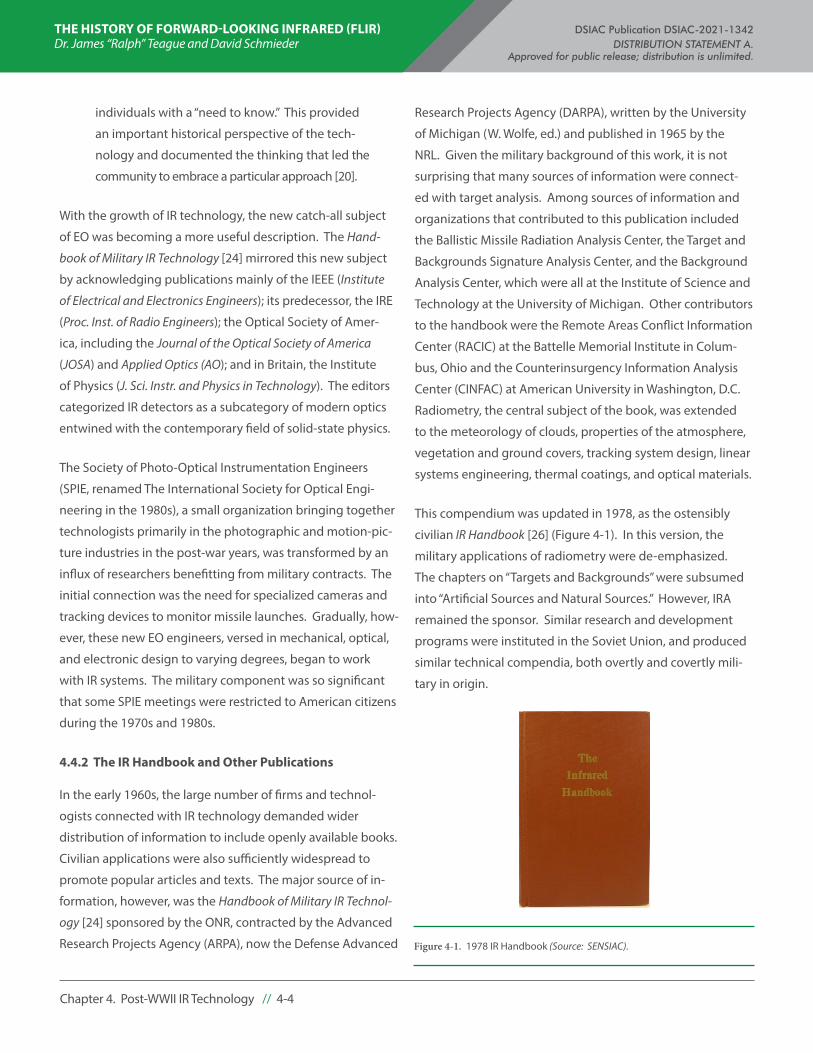
THE HISTORY OF FORWARD-LOOKING INFRARED (FLIR) DSIAC Publication DSIAC-2021-1342 Dr. James “Ralph” Teague and David Schmieder DISTRIBUTION STATEMENT A. Approved for public release; distribution is unlimited.
Chapter 4. Post-WWII IR Technology // 4-4
individuals with a “need to know.” This provided
an important historical perspective of the tech-
nology and documented the thinking that led the
community to embrace a particular approach [20].
With the growth of IR technology, the new catch-all subject
of EO was becoming a more useful description. The Hand-
book of Military IR Technology [24] mirrored this new subject
by acknowledging publications mainly of the IEEE (Institute
of Electrical and Electronics Engineers); its predecessor, the IRE
(Proc. Inst. of Radio Engineers); the Optical Society of Amer-
ica, including the Journal of the Optical Society of America
(JOSA) and Applied Optics (AO); and in Britain, the Institute
of Physics (J. Sci. Instr. and Physics in Technology). The editors
categorized IR detectors as a subcategory of modern optics
entwined with the contemporary field of solid-state physics.
The Society of Photo-Optical Instrumentation Engineers
(SPIE, renamed The International Society for Optical Engi-
neering in the 1980s), a small organization bringing together
technologists primarily in the photographic and motion-pic-
ture industries in the post-war years, was transformed by an
influx of researchers benefitting from military contracts. The
initial connection was the need for specialized cameras and
tracking devices to monitor missile launches. Gradually, how-
ever, these new EO engineers, versed in mechanical, optical,
and electronic design to varying degrees, began to work
with IR systems. The military component was so significant
that some SPIE meetings were restricted to American citizens
during the 1970s and 1980s.
4.4.2 The IR Handbook and Other Publications
In the early 1960s, the large number of firms and technol-
ogists connected with IR technology demanded wider
distribution of information to include openly available books.
Civilian applications were also sufficiently widespread to
promote popular articles and texts. The major source of in-
formation, however, was the Handbook of Military IR Technol-
ogy [24] sponsored by the ONR, contracted by the Advanced
Research Projects Agency (ARPA), now the Defense Advanced
Research Projects Agency (DARPA), written by the University
of Michigan (W. Wolfe, ed.) and published in 1965 by the
NRL. Given the military background of this work, it is not
surprising that many sources of information were connect-
ed with target analysis. Among sources of information and
organizations that contributed to this publication included
the Ballistic Missile Radiation Analysis Center, the Target and
Backgrounds Signature Analysis Center, and the Background
Analysis Center, which were all at the Institute of Science and
Technology at the University of Michigan. Other contributors
to the handbook were the Remote Areas Conflict Information
Center (RACIC) at the Battelle Memorial Institute in Colum-
bus, Ohio and the Counterinsurgency Information Analysis
Center (CINFAC) at American University in Washington, D.C.
Radiometry, the central subject of the book, was extended
to the meteorology of clouds, properties of the atmosphere,
vegetation and ground covers, tracking system design, linear
systems engineering, thermal coatings, and optical materials.
This compendium was updated in 1978, as the ostensibly
civilian IR Handbook [26] (Figure 4-1). In this version, the
military applications of radiometry were de-emphasized.
The chapters on “Targets and Backgrounds” were subsumed
into “Artificial Sources and Natural Sources.” However, IRA
remained the sponsor. Similar research and development
programs were instituted in the Soviet Union, and produced
similar technical compendia, both overtly and covertly mili-
tary in origin.
Figure 4-1. 1978 IR Handbook (Source: SENSIAC).
THE HISTORY OF FORWARD-LOOKING INFRARED (FLIR) DSIAC Publication DSIAC-2021-1342 Dr. James “Ralph” Teague and David Schmieder DISTRIBUTION STATEMENT A. Approved for public release; distribution is unlimited.
Chapter 4. Post-WWII IR Technology // 4-5
The IR Handbook was updated again in 1993 and became an
eight-volume set called The IR & Electro Optical Systems Hand-
book [27]. Several other books were written that significantly
increased the distribution of IR technology and practice.
One of the first, Elements of IR Technology, was written by
Paul Kruse [28] in 1962 at Honeywell. However, IR Systems
Engineering, written by Richard Hudson [22] in 1969 at HAC,
had the most impact. It not only became a standard educa-
tional tool in the U.S. but was widely read in the Soviet Union
as well [29], although the latter was probably not what the
author had intended. This book, although written in 1969,
is still relevant to modern IR systems, and that relevance is
testimony to the knowledge, thoroughness, and expertise of
the author.
4.5 BREAKTHROUGHS IN DETECTOR DEVELOPMENT
4.5.1 PbS Detectors
IR technology progress has always been paced by detector
development progress. Early post-war detector availability
was mostly limited to PbS because of the successful transfer
of that technology from Germany. However, PbS was nomi-
nally only useful in the 1–3-µm band, and it was recognized
just from blackbody radiation principles that the mid-wave
3–5-µm and long-wave 8–12-µm bands offered significant
potential for improvement. For instance, radiation contrast
peaks in the 8–12-µm band for room-temperature objects, so
because sensitivity was at a premium, there was considerable
motivation to exploit the advantage of that region. Missile
seekers and IRSTs are more effective when they can sense jet
engine plume emissions as well as aerodynamically heated
skins for all aspect aircraft detection and tracking. So, they
work best in the 3–5-µm band, at least at short ranges or
high altitudes where there is less atmospheric attenuation
of the plume signature. Besides sensitivity, both the 3–5 and
the 8–12-µm bands, in general, offer a highly transmitting
atmospheric window as well. The advantages of these bands
motivated the development of detectors that responded to
the longer wavelengths of the MWIR and LWIR.
4.5.2 InSb Detectors
Efforts to design better IRSTs and missile seekers led to the
development of cooled photovoltaic InSb. This development
finally resulted in MWIR detectors with sensitivity limited
only by the shot noise in background flux. When cooled,
lead selenide (PbSe) offers response that extends into the
mid-wave band, and cooling reduces internal noise due to
dark current. However, InSb, when cooled to 77 K, performs
far better than PbSe. Moreover, InSb could be prepared in
highly pure, single-crystal form with conventional growth
techniques. This advantage eventually made it producible
and affordable, but it took a great deal of trial and error. The
Hughes Phoenix Search and Track system for the Navy F-14,
circa 1965, was the first significant program using SBRC’s InSb
crystal detectors. The program started using an eight-ele-
ment photoconductive InSb array developed by SBRC and
Honeywell Minneapolis. The early units were delineated by
sandblasting, and both suppliers experienced a great deal
of difficulty with stability and other problems. SBRC finally
developed satisfactory InSb detectors after a change to the
photovoltaic mode, and they ultimately became widely used
in modern FLIRs.
4.5.3 Ge:Hg Detectors
The discovery of the transistor in 1947 also provided im-
portant impetus for advances in detectors. For instance,
transistor research stimulated better growth and purification
techniques in semiconductors. Silicon and germanium (Ge)
were favored semiconductor materials, so methods for impu-
rity insertion became available for these materials first. It was
soon recognized that doping Ge with mercury (Hg) as well
as some other materials would provide response in the LWIR
band [12]. This discovery eventually led Henry Levinstein’s
group at Syracuse University with Air Force funding, and
eventually others, to fabricate Ge:Hg detectors that respond-
ed in the LWIR band. However, these detectors needed to
be cooled to about 28 K and thus needed large, heavy, and
power-hungry, two stage cryocoolers, but they significantly
improved performance. Much later in 1969, the Air Force

THE HISTORY OF FORWARD-LOOKING INFRARED (FLIR) DSIAC Publication DSIAC-2021-1342 Dr. James “Ralph” Teague and David Schmieder DISTRIBUTION STATEMENT A. Approved for public release; distribution is unlimited.
Chapter 4. Post-WWII IR Technology // 4-6
launched the first real production FLIR program when they
procured Ge:Hg detector-based FLIRs for B52 bombers.
4.5.4 HgCdTe (MCT) Detectors
In 1959, a major breakthrough occurred when W. D. Lawson’s
group at the U.K. Royal Radar Establishment (RRE) [30] discov-
ered both photoconductive and photovoltaic response in the
ternary alloy mercury cadmium telluride (HgCdTe, or MCT).
Although this discovery was a breakthrough, the group was
unsuccessful in its attempts to make practical detectors
from MCT. However, shortly thereafter in 1962, Paul Kruse’s
group [31] at the Honeywell Research Center in Minneapolis
developed a crystal growth technique for this alloy in the U.S.
The narrow band gap and variable ratio of its components
allowed the material to be tailored to respond over a wide
spectrum from the near IR to beyond 12 µm. Moreover, the
material was intrinsic with attendant high quantum efficien-
cy in thin detectors. It had a low dielectric constant, which
lowered capacitance to provide rapid temporal response and
the wide bandwidths needed for fast-framing FLIRs. Most
importantly, it provided background-limited noise levels at
the much higher temperature of 77 K. The latter character-
istic allowed using much smaller and more practical cryo-
coolers and Dewars with attendant dramatic reduction in
system size, weight, power, and cost (SWaP-C). Development
of MCT detectors ultimately enabled the mass production
of first-generation FLIRs. However, MCT fabrication was still
difficult, and widespread use of MCT detectors did not occur
until the early 1970s.
The importance of Paul Kruse’s HgCdTe (or MCT) discoveries
at the Honeywell Research Center in Minneapolis cannot be
overestimated. Kruse was a productive scientist and inven-
tor. For instance, he was credited much later for inventing
microbolometer focal plane arrays and they, one might
argue, were destined to have an equally large impact on IR
technology. Fortunately, we have the benefit of transcrip-
tions from Marion Reine’s taped interview with Kruse in
1980. It is so insightful and revealing of the effort and luck
required to fabricate MCT detectors that the interview is
reproduced as Appendix A in this report. What is not widely
known about Lawson’s MCT discovery is that when he and
his colleagues in the U.K. RRE did not immediately succeed in
making viable detectors, they were forced to drop the effort
for many years only to pick it up much later after hearing of
Honeywell’s success. According to U.K. researcher T. Elliott
[32], the RRE was required to drop its MCT research shortly af-
ter Lawson’s breakthrough in order to devote those resources
to developing mid-wave InSb detectors needed for missile
seekers because there was no operational requirement for
LWIR detectors. Paul Kruse and his group, on the other hand,
were able to fabricate reproducible MCT detectors by about
1964 and, after initial papers [31, 33] in the open literature,
published most of their results in classified IRIS proceedings.
While they protected their proprietary techniques, their
success inspired others, such as TI, HAC, and later the British,
French, and Russians, to develop their own techniques, and
the technology soon spread.
Robert Talley [33], president of SBRC during that period,
made some observations that illustrate the payoffs and
challenges that all the competing MCT detector developers
faced:
SBRC got into HgCdTe development in a serious
way. It was clear that this material was going to
be the key long wavelength detector material
of the future.... It required many years of experi-
mentation to develop the necessary techniques
to achieve high quality material. Although each
laboratory bought the purest starting materials,
the resulting purity was not adequate. SBRC’s
approach to purification and crystal growth was
to zone-refine the compounded HgCdTe many
times. By mid-period some detectors showed
performance equivalent to those at Honeywell,
but there were serious problems with yield, stabil-
ity, electrical contacting, and other related issues.
By the end of this period, SBRC still lagged behind
Honeywell.
THE HISTORY OF FORWARD-LOOKING INFRARED (FLIR) DSIAC Publication DSIAC-2021-1342 Dr. James “Ralph” Teague and David Schmieder DISTRIBUTION STATEMENT A. Approved for public release; distribution is unlimited.
Chapter 4. Post-WWII IR Technology // 4-7
SBRC eventually did succeed in making high-quality, produc-
ible MCT detectors. In fact, HAC, through their SBRC subsidi-
ary, ended up being one of the largest suppliers of first-gen-
eration common module detector arrays.
Like many breakthroughs, successful operational MCT
detectors were the result of an accident combined with the
astute recognition of the by-product of that accident. In this
case Kruse reported that, because of a failure in the furnace
used to grow MCT crystals, the molten ingot source material
accidentally cooled instead of remaining in the molten state
as the crystal grew. The result was unintentional annealing of
the MCT compound. That annealed boule was set aside until
months later when an astute technician, Bernice Johnson,
noticed that it showed traces of the same pinkish color that
previously characterized the best performing MCT material.
So, they made detectors out of it and discovered to their sur-
prise that it showed greatly increased detectivity. It was the
breakthrough that showed the way to repeatable fabrication
of highly sensitive, long-wave MCT detectors. The story also
shows how much successful fabrication depended on exper-
imentation instead of in-depth material understanding. It is
also reminiscent of how the Germans achieved success with
PbS and PbSe detectors two decades earlier: not with great
understanding of material science, but with persistent and
time-consuming experimentation and measurement until
success was achieved.
Adoption of MCT for development was not only lucky from
the standpoint that no one knew how to fabricate usable
detectors, even given that it had promising theoretical
properties, but rather MCT had many drawbacks that made
working with it very daunting as it is to this day. For instance,
Hg vapor pressure can be over 20 atmospheres when heated
in crystal growth processes. That pressure caused many labo-
ratory explosions that not only demolished expensive crystal
growth equipment but made whole laboratories unusable
due to dangerous contamination by toxic Hg. Also, MCT
is both soft and brittle, so cutting and polishing it during
fabrication of crystals into detector elements could easily
damage a detector after many hours of labor were expended,
thus making fabrication expensive. These drawbacks caused
many to doubt its viability as a detector candidate even after
its very desirable photosensor properties were understood,
and MCT’s viability is still questioned. Clearly MCT became a
breakthrough material because it offered ideal sensitivity in
the LWIR band at 77 K temperature, but it still would not have
emerged when it did if it were not for luck, knowledge, and
persistence together with years of government funding
and corporate management’s support of their research
laboratories.
4.6 DEVELOPMENT OF IRST SYSTEMS (ADAPTED FROM
ROBERT SENDALL’S SENSIAC REPORTS [19])
The development of IRSTs helped to advance a baseline of
enabling technology that soon contributed to the emer-
gence of FLIRs as well. As previously stated, IRST sets have
been used in various forms since WWII, even though they
were not called that before about 1960. The IRST is a passive
sensor that uses heat emitted by the target to generate data
for the weapon system of an aircraft or other platforms such
as ships or anti-aircraft batteries. Passive operation of the
IRST has the advantage of concealment. In addition, it can
be designed with an auxiliary narrow field of view (FOV) to
provide high-resolution imaging for long-range visual identi-
fication when the image is presented on a display [19].
Using sensors that detect heat in searching for targets from
combat aircraft is as old as the use of these sensors for missile
guidance. The first models exhibited limited performance
in that a target image was not formed. Instead they relied
on nonimaging techniques such as a scanning reticle or a
scanned cross array in a cruciform configuration to determine
a target’s position without forming a displayed image. Other
early IRST designs would raster scan the scene with detector
line arrays to show target position by means of symbology
positioned on a head-up display. These early versions had
difficulty with high false-alarm rates due to low resolution
and clutter such as sunlit cloud edges and ground objects.
Much like FLIRs, current IRSTs show high-resolution imagery
on a monitor, so the operators can see the objects to help
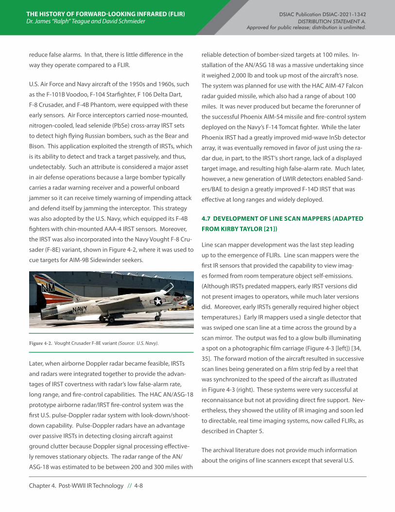
THE HISTORY OF FORWARD-LOOKING INFRARED (FLIR) DSIAC Publication DSIAC-2021-1342 Dr. James “Ralph” Teague and David Schmieder DISTRIBUTION STATEMENT A. Approved for public release; distribution is unlimited.
Chapter 4. Post-WWII IR Technology // 4-8
reduce false alarms. In that, there is little difference in the
way they operate compared to a FLIR.
U.S. Air Force and Navy aircraft of the 1950s and 1960s, such
as the F-101B Voodoo, F-104 Starfighter, F 106 Delta Dart,
F-8 Crusader, and F-4B Phantom, were equipped with these
early sensors. Air Force interceptors carried nose-mounted,
nitrogen-cooled, lead selenide (PbSe) cross-array IRST sets
to detect high flying Russian bombers, such as the Bear and
Bison. This application exploited the strength of IRSTs, which
is its ability to detect and track a target passively, and thus,
undetectably. Such an attribute is considered a major asset
in air defense operations because a large bomber typically
carries a radar warning receiver and a powerful onboard
jammer so it can receive timely warning of impending attack
and defend itself by jamming the interceptor. This strategy
was also adopted by the U.S. Navy, which equipped its F-4B
fighters with chin-mounted AAA-4 IRST sensors. Moreover,
the IRST was also incorporated into the Navy Vought F-8 Cru-
sader (F-8E) variant, shown in Figure 4-2, where it was used to
cue targets for AIM-9B Sidewinder seekers.
Later, when airborne Doppler radar became feasible, IRSTs
and radars were integrated together to provide the advan-
tages of IRST covertness with radar’s low false-alarm rate,
long range, and fire-control capabilities. The HAC AN/ASG-18
prototype airborne radar/IRST fire-control system was the
first U.S. pulse-Doppler radar system with look-down/shoot-
down capability. Pulse-Doppler radars have an advantage
over passive IRSTs in detecting closing aircraft against
ground clutter because Doppler signal processing effective-
ly removes stationary objects. The radar range of the AN/
ASG-18 was estimated to be between 200 and 300 miles with
reliable detection of bomber-sized targets at 100 miles. In-
stallation of the AN/ASG 18 was a massive undertaking since
it weighed 2,000 lb and took up most of the aircraft’s nose.
The system was planned for use with the HAC AIM-47 Falcon
radar guided missile, which also had a range of about 100
miles. It was never produced but became the forerunner of
the successful Phoenix AIM-54 missile and fire-control system
deployed on the Navy’s F-14 Tomcat fighter. While the later
Phoenix IRST had a greatly improved mid-wave InSb detector
array, it was eventually removed in favor of just using the ra-
dar due, in part, to the IRST’s short range, lack of a displayed
target image, and resulting high false-alarm rate. Much later,
however, a new generation of LWIR detectors enabled Sand-
ers/BAE to design a greatly improved F-14D IRST that was
effective at long ranges and widely deployed.
4.7 DEVELOPMENT OF LINE SCAN MAPPERS (ADAPTED
FROM KIRBY TAYLOR [21])
Line scan mapper development was the last step leading
up to the emergence of FLIRs. Line scan mappers were the
first IR sensors that provided the capability to view imag-
es formed from room temperature object self-emissions.
(Although IRSTs predated mappers, early IRST versions did
not present images to operators, while much later versions
did. Moreover, early IRSTs generally required higher object
temperatures.) Early IR mappers used a single detector that
was swiped one scan line at a time across the ground by a
scan mirror. The output was fed to a glow bulb illuminating
a spot on a photographic film carriage (Figure 4-3 [left]) [34,
35]. The forward motion of the aircraft resulted in successive
scan lines being generated on a film strip fed by a reel that
was synchronized to the speed of the aircraft as illustrated
in Figure 4-3 (right). These systems were very successful at
reconnaissance but not at providing direct fire support. Nev-
ertheless, they showed the utility of IR imaging and soon led
to directable, real time imaging systems, now called FLIRs, as
described in Chapter 5.
The archival literature does not provide much information
about the origins of line scanners except that several U.S.
Figure 4-2. Vought Crusader F-8E variant (Source: U.S. Navy).
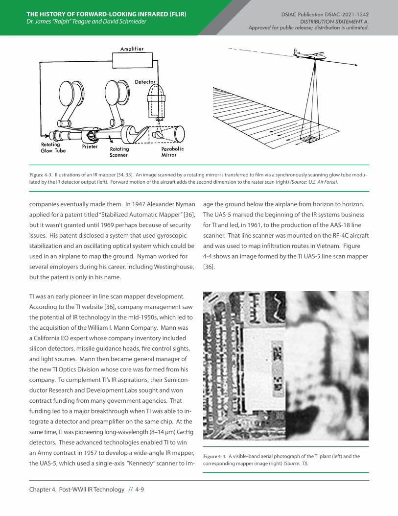
THE HISTORY OF FORWARD-LOOKING INFRARED (FLIR) DSIAC Publication DSIAC-2021-1342 Dr. James “Ralph” Teague and David Schmieder DISTRIBUTION STATEMENT A. Approved for public release; distribution is unlimited.
Chapter 4. Post-WWII IR Technology // 4-9
companies eventually made them. In 1947 Alexander Nyman
applied for a patent titled “Stabilized Automatic Mapper” [36],
but it wasn’t granted until 1969 perhaps because of security
issues. His patent disclosed a system that used gyroscopic
stabilization and an oscillating optical system which could be
used in an airplane to map the ground. Nyman worked for
several employers during his career, including Westinghouse,
but the patent is only in his name.
TI was an early pioneer in line scan mapper development.
According to the TI website [36], company management saw
the potential of IR technology in the mid-1950s, which led to
the acquisition of the William I. Mann Company. Mann was
a California EO expert whose company inventory included
silicon detectors, missile guidance heads, fire control sights,
and light sources. Mann then became general manager of
the new TI Optics Division whose core was formed from his
company. To complement TI’s IR aspirations, their Semicon-
ductor Research and Development Labs sought and won
contract funding from many government agencies. That
funding led to a major breakthrough when TI was able to in-
tegrate a detector and preamplifier on the same chip. At the
same time, TI was pioneering long-wavelength (8–14 µm) Ge:Hg
detectors. These advanced technologies enabled TI to win
an Army contract in 1957 to develop a wide-angle IR mapper,
the UAS-5, which used a single-axis “Kennedy” scanner to im-
age the ground below the airplane from horizon to horizon.
The UAS-5 marked the beginning of the IR systems business
for TI and led, in 1961, to the production of the AAS-18 line
scanner. That line scanner was mounted on the RF-4C aircraft
and was used to map infiltration routes in Vietnam. Figure
4-4 shows an image formed by the TI UAS-5 line scan mapper
[36].
Figure 4-3. Illustrations of an IR mapper [34, 35]. An image scanned by a rotating mirror is transferred to film via a synchronously scanning glow tube modu-lated by the IR detector output (left). Forward motion of the aircraft adds the second dimension to the raster scan (right) (Source: U.S. Air Force).
Figure 4-4. A visible-band aerial photograph of the TI plant (left) and the corresponding mapper image (right) (Source: TI).
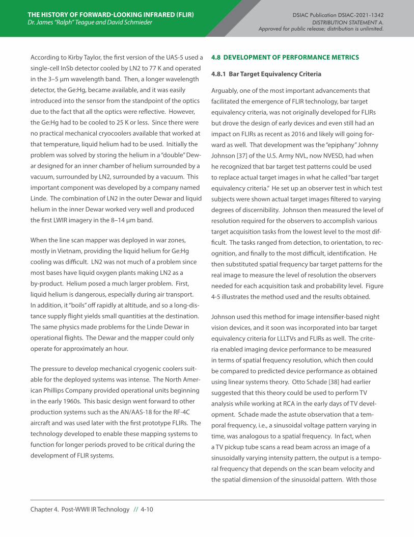
THE HISTORY OF FORWARD-LOOKING INFRARED (FLIR) DSIAC Publication DSIAC-2021-1342 Dr. James “Ralph” Teague and David Schmieder DISTRIBUTION STATEMENT A. Approved for public release; distribution is unlimited.
Chapter 4. Post-WWII IR Technology // 4-10
According to Kirby Taylor, the first version of the UAS-5 used a
single-cell InSb detector cooled by LN2 to 77 K and operated
in the 3–5 µm wavelength band. Then, a longer wavelength
detector, the Ge:Hg, became available, and it was easily
introduced into the sensor from the standpoint of the optics
due to the fact that all the optics were reflective. However,
the Ge:Hg had to be cooled to 25 K or less. Since there were
no practical mechanical cryocoolers available that worked at
that temperature, liquid helium had to be used. Initially the
problem was solved by storing the helium in a “double” Dew-
ar designed for an inner chamber of helium surrounded by a
vacuum, surrounded by LN2, surrounded by a vacuum. This
important component was developed by a company named
Linde. The combination of LN2 in the outer Dewar and liquid
helium in the inner Dewar worked very well and produced
the first LWIR imagery in the 8–14 µm band.
When the line scan mapper was deployed in war zones,
mostly in Vietnam, providing the liquid helium for Ge:Hg
cooling was difficult. LN2 was not much of a problem since
most bases have liquid oxygen plants making LN2 as a
by-product. Helium posed a much larger problem. First,
liquid helium is dangerous, especially during air transport.
In addition, it “boils” off rapidly at altitude, and so a long-dis-
tance supply flight yields small quantities at the destination.
The same physics made problems for the Linde Dewar in
operational flights. The Dewar and the mapper could only
operate for approximately an hour.
The pressure to develop mechanical cryogenic coolers suit-
able for the deployed systems was intense. The North Amer-
ican Phillips Company provided operational units beginning
in the early 1960s. This basic design went forward to other
production systems such as the AN/AAS-18 for the RF-4C
aircraft and was used later with the first prototype FLIRs. The
technology developed to enable these mapping systems to
function for longer periods proved to be critical during the
development of FLIR systems.
4.8 DEVELOPMENT OF PERFORMANCE METRICS
4.8.1 Bar Target Equivalency Criteria
Arguably, one of the most important advancements that
facilitated the emergence of FLIR technology, bar target
equivalency criteria, was not originally developed for FLIRs
but drove the design of early devices and even still had an
impact on FLIRs as recent as 2016 and likely will going for-
ward as well. That development was the “epiphany” Johnny
Johnson [37] of the U.S. Army NVL, now NVESD, had when
he recognized that bar target test patterns could be used
to replace actual target images in what he called “bar target
equivalency criteria.” He set up an observer test in which test
subjects were shown actual target images filtered to varying
degrees of discernibility. Johnson then measured the level of
resolution required for the observers to accomplish various
target acquisition tasks from the lowest level to the most dif-
ficult. The tasks ranged from detection, to orientation, to rec-
ognition, and finally to the most difficult, identification. He
then substituted spatial frequency bar target patterns for the
real image to measure the level of resolution the observers
needed for each acquisition task and probability level. Figure
4-5 illustrates the method used and the results obtained.
Johnson used this method for image intensifier-based night
vision devices, and it soon was incorporated into bar target
equivalency criteria for LLLTVs and FLIRs as well. The crite-
ria enabled imaging device performance to be measured
in terms of spatial frequency resolution, which then could
be compared to predicted device performance as obtained
using linear systems theory. Otto Schade [38] had earlier
suggested that this theory could be used to perform TV
analysis while working at RCA in the early days of TV devel-
opment. Schade made the astute observation that a tem-
poral frequency, i.e., a sinusoidal voltage pattern varying in
time, was analogous to a spatial frequency. In fact, when
a TV pickup tube scans a read beam across an image of a
sinusoidally varying intensity pattern, the output is a tempo-
ral frequency that depends on the scan beam velocity and
the spatial dimension of the sinusoidal pattern. With those

THE HISTORY OF FORWARD-LOOKING INFRARED (FLIR) DSIAC Publication DSIAC-2021-1342 Dr. James “Ralph” Teague and David Schmieder DISTRIBUTION STATEMENT A. Approved for public release; distribution is unlimited.
Chapter 4. Post-WWII IR Technology // 4-11
equivalents in place, Schade recognized that the same linear
systems theory, including the powerful Transfer Function,
which characterized electrical system temporal frequency
response, was just as applicable to characterizing optical and
EO image-forming system response. This discovery gener-
ated the equivalent transfer function metric, later called the
Modulation Transfer Function (or MTF). The MTF was used
by both optical and EO engineers to quantify the resolution
of their respective systems. Since EO systems consist of both
optics and electronics, MTF proved to be a convenient metric
for quantifying the resolution performance of the combined
systems.
Schade’s and Johnson’s work not only helped to base FLIR
design and performance analysis on sound engineering
principles, but it also provided the measurement-based
criteria they needed to meet for evaluation and comparison
between approaches. Fred Rosell [39] at Westinghouse ex-
tended the basic theoretical and psychophysical framework
when he studied the effects of system noise on observer
performance again using TV systems. Though the work
of these three pioneers provided a very important foun-
dation, it was still not directly applicable to FLIRs but Bob
Sendall at HAC developed a similar framework for FLIRs and
later worked with Rosell [40] to merge their modeling and
empirical performance data so they applied to both FLIRs
and TVs in a common methodology. In the case of FLIRs,
Sendall developed the Minimum Resolvable Temperature
(MRT) metric, which combined the effects of both noise and
resolution on performance as seen by an observer viewing
imagery on a FLIR display. This fundamental performance
analysis approach and criteria allowed FLIRs to be designed
to meet specific user performance objectives and allowed
government procurement officials to rigorously compare
competing designs. James Ratches [41] at NVL later incorpo-
rated the methodology in a FORTRAN computer code that
Figure 4-5. Johnson’s Bar Target Equivalency Criteria determined resolution requirements for various target acquisition tasks [37] (Source: U.S. Army).
THE HISTORY OF FORWARD-LOOKING INFRARED (FLIR) DSIAC Publication DSIAC-2021-1342 Dr. James “Ralph” Teague and David Schmieder DISTRIBUTION STATEMENT A. Approved for public release; distribution is unlimited.
Chapter 4. Post-WWII IR Technology // 4-12
became the first of many NVL/NVESD models that were wide-
ly disseminated to the IR community as a design tool. As of
2016, these basic criteria and models were still being used to
design current FLIRs. Both the criteria and the models have
been continuously refined to incorporate the most recent
measurement data and new modeling insights as will be dis-
cussed in Chapter 9.4. Ultimately, their work developed into
a new engineering discipline: EO systems engineering.
4.9 SUMMARY AND CONCLUSIONS
Immediately following WWII and leading up to the Vietnam
War, there was substantial development of IR infrastruc-
ture and enabling technology. Key contributions included
better communication of IR research, better detectors, new
scanning system technology, and new performance metrics.
However, a viable, fast-framing FLIR was not produced during
this period; that achievement occurred during the Vietnam
War as is described in Chapter 5.
THE HISTORY OF FORWARD-LOOKING INFRARED (FLIR) DSIAC Publication DSIAC-2021-1342 Dr. James “Ralph” Teague and David Schmieder DISTRIBUTION STATEMENT A. Approved for public release; distribution is unlimited.
Chapter 5. Vietnam-Era FLIR Development // 5-1
CHAPTER 5. VIETNAM-ERA FLIR DEVELOPMENT5.1 INTRODUCTION
During the Vietnam War era (1964–1973), the first practical,
fast-framing FLIRs were developed. Many companies and
government organizations contributed to their development.
However, two companies played the largest role: HAC with
its subsidiary SBRC (became RVS) and TI (portions of TI later
became DRS). Others such as Aerojet General, Honeywell (to
become BAE), and AVCO (became CE, then L-3) were com-
petitors and made key contributions but had lesser overall
roles at the system level during this era. The recollections in
this chapter of key contributors Robert Sendal [19] (HAC) and
Kirby Taylor [21] (TI) provide valuable and insightful observa-
tions about the struggles to perfect FLIR technology and how
they overcame adversity. These observations can help future
developers understand what it takes to succeed in a corpo-
rate/government/war-time procurement environment.
Important contributions to both FLIR development and FLIR
history documentation were also made by J. Michael Lloyd
at Honeywell and Lucien M. Biberman at the Institute for
Defense Analysis (IDA). According to Lloyd [42], fast-fram-
ing thermal imagers were not feasible before the late 1950s
because detector bandwidths had to be limited to a few
hundred hertz due to poor detector time response. However,
detector time constants got shorter with the emergence of
cooled InSb and Ge:Hg, which combined with their mid- and
long-wavelength spectral response, enabled strip mappers
to become practical. He reported that the first LWIR FLIR
was built in 1956 during the Korean War at the University of
Chicago, with Air Force support, by modifying an AN/AAS-3
strip mapper that was designated the XA-1. It was made by
adding a nodding elevation mirror to the existing horizontal
scanner. Development was not pursued when the war end-
ed, since there was no longer a pressing need.
Lloyd also reported that the Army developed one of the first
FLIRs in 1960, when it funded Perkin-Elmer Corporation to
build a ground-based FLIR. It reportedly used two rotating,
refractive prisms, which performed a spiral scan of a sin-
gle-element InSb detector over a 5° diameter circular FOV
with a 1-milliradian instantaneous FOV (IFOV). The FLIR had
a 5-Hz frame rate and an approximate 1.0 °C sensitivity. The
flicker problem caused by such a slow frame rate was man-
aged by using a long persistence phosphor cathode ray tube
(CRT) display.
However, the Air Force Avionics Laboratory (AFAL) at
Wright-Patterson AFB in Dayton, Ohio had the most influence
of the government agencies in this era for two reasons. First,
the Air Force needed strategic bombers to be equipped with
FLIRs during the Cold War for low-altitude night navigation to
avoid radar detection and for nuclear blast blindness protec-
tion when flying into the Soviet Union. Second, the Vietnam
War began and the Air Force mission in Vietnam involved
heavy roles in surveillance and interdiction. Those roles led
them to have the earliest need to develop FLIR technology.
Captain James Krause took the initiative to promote FLIR
technology development and, as a result, not only became
the Air Force’s lead combat FLIR user but was very influential
in the IR community. His feedback and design suggestions
from a user standpoint, including his many presentations at
IRIS/MSS meetings, had a major impact on the direction of
FLIR development and use.
In addition to the Air Force’s early pressing needs, both Navy
and Army agencies had urgent needs and were involved in
FLIR development as well. For instance, the Navy at China
Lake experimented with FLIRs for P2A and RA-5 surveillance
aircraft, and the Army explored them for use on their OV-10
Mohawk battlefield support aircraft. Both the Navy and the
Army embraced FLIR technology and later became major
sources of development and funding.
The role of Lucien Biberman at IDA was central in early FLIR
development. IDA is a quasi-governmental, nonprofit Feder-
THE HISTORY OF FORWARD-LOOKING INFRARED (FLIR) DSIAC Publication DSIAC-2021-1342 Dr. James “Ralph” Teague and David Schmieder DISTRIBUTION STATEMENT A. Approved for public release; distribution is unlimited.
Chapter 5. Vietnam-Era FLIR Development // 5-2
ally Funded Research & Development Center (FFRDC) created
in 1956 to provide scientific and technical expertise to the
Department of Defense (DoD). Biberman was widely respect-
ed for his role in creating the highly successful Sidewinder
missile and for his technical savvy. He was always ready to
voice his opinions at both formal and informal meetings if he
thought programs were going in the wrong direction, even
at the risk of offending powerful program interests. Biber-
man was puzzled by the performance disparity among early
FLIRs and forced flight tests to compare competing systems.
When the disparate results could not be explained, he real-
ized that critical design parameters such as noise equivalent
temperature (NET), frame rate, and apparent display size
were not understood and were potentially not even all inclu-
sive. He headed a committee of government and industry
experts to define a performance model that would guide
design specifications for future systems.
The urgent need for night viewing in Vietnam incentivized
the military and defense companies to rapidly develop IR
technology. HAC and TI were early competitors, and each
took a different approach. In the end, TI equipment played
the largest role and led to the development of the first-gen-
eration Common Module (“Mod”) FLIR after the war. TI FLIRs
used a more direct and simpler optomechanical design
than HAC FLIRs, which minimized the need for still nascent
multiplexing electronics. At first they used modified CRTs
for display, but eventually progressed to simple, standard
TV cameras to view and convert parallel output channels for
serial display on standard monitors. HAC FLIRs were more
complex and more difficult to build. They incorporated
special electronics to implement detector-staggered spacing
for cold shielding that required unique output multiplexing
and time delay to register the resulting output for image
display. However, the output was still not standard TV com-
patible, so it required a special nonstandard CRT display. The
TI approach was more producible in this early era, but many
attributes of the HAC multiplexer design were eventually
incorporated into postwar designs and second generation
(GEN2) FLIRs. HAC, under the leadership of Robert Sendall,
also led the way in the development of performance metrics,
which were instrumental in optimizing system performance
by quantifying the effects of both the system design parame-
ters and the observer viewing the displayed image. All of this
technological improvement would have happened eventual-
ly, but the incentives of the Vietnam War accelerated it during
this era.
5.2 VIETNAM WAR IR IMAGING PROBLEMS AND
SOLUTIONS
IR systems were extremely important during the Vietnam
War, which involved jungle warfare against an elusive, often
well concealed, enemy who preferred night operations.
This highlighted the importance of IR systems. Airborne,
down-looking line scanners, initially mounted in C-47 trans-
port aircraft, were the first IR systems in theater. As described
in Section 4.2, these systems scanned a single, LN2-cooled,
InSb photodiode detector back and forth across the flight
path using the detector output to drive a miniature arc lamp
that exposed a strip of photographic film. The film was de-
veloped after the aircraft returned to base and was examined
by image analysts for signs of enemy activity. This method
proved to be quite unsatisfactory (except for certain fixed tar-
gets), since the time delay between flyover and subsequent
attack by strike aircraft was 4–6 hr. In spite of this drawback,
over 1,000 line scanner systems were deployed on RF4C,
B57, RA5-C, and OV-1 Mohawk aircraft in waves of improving
technology throughout the 1960s. Improvements included
replacement of single-element detectors with small arrays of
detectors, replacement of InSb with Ge:Hg detectors (halving
the NET difference), and replacement of the arc lamp with
gallium arsenide (GaAs) diodes. In a final line-scanner ver-
sion, film was developed on-board in near real-time, allowing
the crew to locate targets and vector in strike aircraft within
minutes. Real-time viewers were developed to see a near re-
al-time moving map display in the aircraft. This method was
better than developing film, but the detected targets were
always behind the aircraft by the time the operator could
see them. So this modification was also unsatisfactory when
tracking moving targets.
THE HISTORY OF FORWARD-LOOKING INFRARED (FLIR) DSIAC Publication DSIAC-2021-1342 Dr. James “Ralph” Teague and David Schmieder DISTRIBUTION STATEMENT A. Approved for public release; distribution is unlimited.
Chapter 5. Vietnam-Era FLIR Development // 5-3
An IR system capable of fast-frame imaging was needed for a
combatant to find his target, track it in real-time, and deliver
a munition without ever breaking contact. He could control
the entire kill chain and minimize latency.
Such a system, which became known as FLIR, was devel-
oped by the Air Force and TI in 1964. It was then mounted
in a C-47 transport aircraft that had been converted into a
gunship and deployed to Vietnam in 1965. The FLIR and
its immediate successors made a dramatic impact on the
battlefield. For the first time, traffic along the Ho Chi Minh
Trail was interdicted effectively, and even small units of Viet
Cong moving through foliated countryside were frequently
detected.
The first FLIRs used 40-mil (i.e., approx. 1,000 µm) Ge:Hg LWIR
detectors in 1x3 and, later, in 2x15 parallel/serial array config-
urations with mirrors to scan them across and down the FOV
every 20 milliseconds (50-Hz frame rate). Output from the
detectors was used to modulate the intensity of a Matricon
CRT that was directly viewed by an operator. But the FLIRs
were expensive, large, heavy (approximately 600 lb), energy
inefficient (approximately 1,000 W), and the image quality
was less than ideal. In addition, their wide FOV with relatively
low resolution was not practical for longer range fire control
systems.
These problems were addressed with technological improve-
ments between 1968 and the end of U.S. involvement in the
war in 1972. One improvement introduced larger, one-di-
mensional parallel scanners using linear arrays of up to 400
channels with much smaller Ge:Hg detector sizes that were
on the order of 3 mils square. These image-plane scanned
arrays sensed the IR imagery through relatively long focal
length refractive lenses. Twelve-inch focal lengths with 3-mil
elements produced resolutions of 1/4 milliradian. Optical
switching mechanisms provided for on-command selection
of wide and narrow FOV. Signal processing was achieved by
EO multiplexer imaging light-emitting diodes (LEDs) format-
ted in the same geometry as the detectors and scanned off
a mirror assembly connected directly to the IR scanner. This
concept was a forerunner of the next-generation Common
Module FLIR approach.
Another major improvement occurred in 1970 when Ge:Hg
detectors were replaced by the first production LWIR MCT
photoconductive detectors. MCT is a nearly ideal, intrinsic,
photodetector material, with a direct, compositionally tailor-
able, bandgap as opposed to Ge:Hg, which has an extrinsic,
fixed, indirect bandgap. Consequently, MCT detectors have a
much higher photon absorption coefficient (providing better
sensitivity with thinner detectors), much lower dark current
(enabling higher operating temperatures), and a bandgap
tuned exactly to the LWIR atmospheric window (enabling
maximum signal-to-noise ratio). Much smaller 2-mil MCT
detectors were made in 1x180 parallel configurations, cooled
to 77 K (instead of 28 K for Ge:Hg), and interlace scanned
(for 360 lines of resolution). These higher-temperature
systems with smaller detectors that allowed smaller optics as
well were much less expensive to build, were one-third the
volume of Ge:Hg detectors, weighed only 200 lb, consumed
much less power, and exhibited exceptionally crisp imagery.
Alternative solutions to FLIRs for night vision were also
intensely investigated during the war. LLTVs were prime
candidates. In their most basic form, LLTVs combined a mul-
tistage image intensifier with a vidicon. Ambient light was
insufficient for the poor quantum efficiency photocathodes,
and spectral response did not extend far enough into the
near IR to detect significant sky glow as did later image inten-
sifiers. Covert active illumination was added by placing filters
on artificial sources such as xenon lamps. After lasers were
invented in the early 1960s and practical neodymium-doped
yttrium aluminum garnet (Nd:YAG) lasing media provided
invisible 1.06-µm laser light in the mid to late 1960s, active
THE HISTORY OF FORWARD-LOOKING INFRARED (FLIR) DSIAC Publication DSIAC-2021-1342 Dr. James “Ralph” Teague and David Schmieder DISTRIBUTION STATEMENT A. Approved for public release; distribution is unlimited.
Chapter 5. Vietnam-Era FLIR Development // 5-4
pulse-gated LLTVs4 appeared to be a viable competitor to
FLIRs. Since a major concern was seeing through battle-
field smoke and dust, the systems were pulse-gated so that
discrete pulse returns were timed to correspond to ranges
near the target. Image intensifiers on the LLTVs had rapid
response and could be shuttered to open at the intended
pulse return time and then closed to lock out reflections from
shorter range aerosols. This technique gated out inter-
mediate range returns from dust and smoke. According to
Ponomarenko and Filachev [29], the Russians experimented
with similar night vision approaches and built a prototype
device using a ruby laser in 1963.
Pulse-gated LLTVs had several drawbacks compared to FLIRs
including the poor penetration power of their shorter wave-
lengths, and the fact that they were active raised concerns
that they were not sufficiently covert. In that era, they were
soon replaced by FLIRs, but they later re-emerged in more
modern fire-control systems as complements to FLIRs. They
can complement FLIRs due to their ability to provide ex-
tra-long target identification range by exploiting their much
shorter wavelengths to obtain smaller optical diffraction blur
spot sizes and thus higher resolution.
5.3 TI FLIR DEVELOPMENT [21]
This subsection is a history of FLIR development at TI as
extracted, edited, and condensed from the recollections of
Kirby Taylor. Also included is historical information from TI’s
website [43] where the latter is then further expanded with
inputs from Taylor for this history. However, information
from other sources is also included, and those sources are
specifically cited. Taylor, an electrical engineer, was uniquely
positioned to provide historical recollections. He witnessed
first-hand the engineering and the political struggles both
as a contributor to the FLIR design process and as a contrac-
tor field support engineer in the Vietnam theater. Taylor’s
informative stories of those struggles provide insight into the
4 Coauthor David Schmieder was on the team under Army contract to integrate pulse-gated LLTVs into tank fire-control systems while employed by Delco Division of General Motors in 1970.
challenges of war-time technology insertion. Some of them
are included in Appendix B.
5.3.1 First FLIR System: FLIR 1
In 1963, TI engineers began to develop a real-time, two
dimensional IR viewer with $30,000 in company funding. The
approach was to investigate the feasibility of adding a sec-
ond scan mirror to the single-axis line scanner, which would
supplant the forward motion of the aircraft as a means to
generate the second scan direction. This real-time IR imaging
device was called FLIR–Forward-Looking Infrared. The name
came from the fact that the previous devices were mappers
that looked down, but the new, two dimensional scanner was
now able to look forward. The study included some basic
scanning experiments that determined the concept’s feasi-
bility. TI hurriedly prepared an unsolicited proposal to ARPA,
later renamed DARPA. DARPA’s charter was to investigate
high-risk, but high-payoff, visionary new technologies and
was, in a sense, the “venture capital” arm of the DoD.
DARPA said the concept was interesting but there was no
military requirement for a FLIR because combat was not
conducted at night. While obviously disappointed by this re-
sponse, TI persisted and approached the AFAL at Wright-Pat-
terson AFB, which had been previously involved with TI in
line-scanner source selection and in detector development.
The Air Force saw value in night imaging but required TI to
bid on the project in an open competition. TI’s idea was no
longer considered proprietary, and eight companies compet-
ed for one of the two $250,000 contracts. However, all com-
petitors eventually dropped out and the award went to TI.
TI began work in October 1964 with a dedicated team of
physicists and engineers. In May 1965, the first exploratory
flight test was conducted. A major factor in this accomplish-
ment was having access to a detector factory, cryogenics
from ongoing mapper programs, the baseline Kennedy scan-
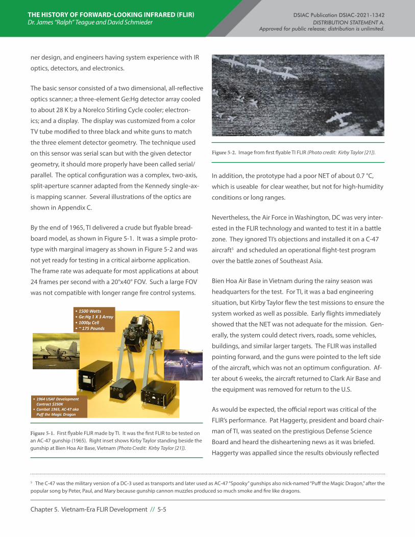
THE HISTORY OF FORWARD-LOOKING INFRARED (FLIR) DSIAC Publication DSIAC-2021-1342 Dr. James “Ralph” Teague and David Schmieder DISTRIBUTION STATEMENT A. Approved for public release; distribution is unlimited.
Chapter 5. Vietnam-Era FLIR Development // 5-5
ner design, and engineers having system experience with IR
optics, detectors, and electronics.
The basic sensor consisted of a two dimensional, all-reflective
optics scanner; a three-element Ge:Hg detector array cooled
to about 28 K by a Norelco Stirling Cycle cooler; electron-
ics; and a display. The display was customized from a color
TV tube modified to three black and white guns to match
the three element detector geometry. The technique used
on this sensor was serial scan but with the given detector
geometry, it should more properly have been called serial/
parallel. The optical configuration was a complex, two-axis,
split-aperture scanner adapted from the Kennedy single-ax-
is mapping scanner. Several illustrations of the optics are
shown in Appendix C.
By the end of 1965, TI delivered a crude but flyable bread-
board model, as shown in Figure 5-1. It was a simple proto-
type with marginal imagery as shown in Figure 5-2 and was
not yet ready for testing in a critical airborne application.
The frame rate was adequate for most applications at about
24 frames per second with a 20°x40° FOV. Such a large FOV
was not compatible with longer range fire control systems.
5 The C-47 was the military version of a DC-3 used as transports and later used as AC-47 “Spooky” gunships also nick-named “Puff the Magic Dragon,” after the popular song by Peter, Paul, and Mary because gunship cannon muzzles produced so much smoke and fire like dragons.
In addition, the prototype had a poor NET of about 0.7 °C,
which is useable for clear weather, but not for high-humidity
conditions or long ranges.
Nevertheless, the Air Force in Washington, DC was very inter-
ested in the FLIR technology and wanted to test it in a battle
zone. They ignored TI’s objections and installed it on a C-47
aircraft5 and scheduled an operational flight-test program
over the battle zones of Southeast Asia.
Bien Hoa Air Base in Vietnam during the rainy season was
headquarters for the test. For TI, it was a bad engineering
situation, but Kirby Taylor flew the test missions to ensure the
system worked as well as possible. Early flights immediately
showed that the NET was not adequate for the mission. Gen-
erally, the system could detect rivers, roads, some vehicles,
buildings, and similar larger targets. The FLIR was installed
pointing forward, and the guns were pointed to the left side
of the aircraft, which was not an optimum configuration. Af-
ter about 6 weeks, the aircraft returned to Clark Air Base and
the equipment was removed for return to the U.S.
As would be expected, the official report was critical of the
FLIR’s performance. Pat Haggerty, president and board chair-
man of TI, was seated on the prestigious Defense Science
Board and heard the disheartening news as it was briefed.
Haggerty was appalled since the results obviously reflected
Figure 5-1. First flyable FLIR made by TI. It was the first FLIR to be tested on an AC-47 gunship (1965). Right inset shows Kirby Taylor standing beside the gunship at Bien Hoa Air Base, Vietnam (Photo Credit: Kirby Taylor [21]).
Figure 5-2. Image from first flyable TI FLIR (Photo credit: Kirby Taylor [21]).

THE HISTORY OF FORWARD-LOOKING INFRARED (FLIR) DSIAC Publication DSIAC-2021-1342 Dr. James “Ralph” Teague and David Schmieder DISTRIBUTION STATEMENT A. Approved for public release; distribution is unlimited.
Chapter 5. Vietnam-Era FLIR Development // 5-6
poorly on TI and it eroded his support for further internal
FLIR development. However, other managers, such as Ray
McCord, still strongly believed in FLIR technology. McCord
continued to press for resources to finance, for instance,
critical IR detectors even as skeptical management cut overall
research funding. He was determined to keep it a priority
even as many in TI were willing to either eliminate or down-
grade the importance of the IR program.
Despite the FLIR’s poor performance in Vietnam, DoD leader-
ship realized the importance of FLIR technology, particularly
as part of the circling gunship concept. They felt that during
night missions, having an onboard FLIR to locate and recog-
nize targets was critical because it would allow the aircraft to
accomplish the mission it was intended for: to attack targets,
especially ground truck convoys, by circling at a constant
altitude and firing large-caliber guns. Whereas the gunship’s
effectiveness was initially thwarted because the enemy hid
during the day and moved at night, FLIR technology, much
more than flares or low-light-level TV, enabled these aircraft
to complete missions at night. Therefore, in spite of the Air
Force’s disappointment with the FLIR lab model, they award-
ed TI a million dollar contract for continued FLIR develop-
ment. TI then successfully produced a series of gunship FLIR
systems capable of detecting targets at increasing ranges.
Key DoD supporters backed TI’s efforts, but they also pressed
for results. In one case, Air Force Major Jim Krause appealed
directly to McCord to urge for improved performance.
McCord, with company support, responded with a commit-
ment to solve remaining problems without additional cost
to the customer. As a result, TI successfully produced a series
of gunship FLIR systems capable of detecting targets at ever
longer ranges. Krause, now a lieutenant colonel, went on
to fly hundreds of missions including those on the newly
introduced and more capable Spectre AC-130 gunships. He
taught new operators and observed performance character-
istics to provide direct feedback to development engineers.
Taylor personally saw him return from a mission on one
plane, jump off, and run to board another outbound plane to
fly the next mission. Promoted to colonel, Jim Krause went
on to become Director of the Air Force Avionics Lab.
5.3.2 FLIR Design Progression
FLIR II. The experience gained in these earlier programs
was devoted to developing an improved version of FLIR
using a 15x2 Ge:Hg detector array. In the FLIR II, the NET (per
channel) was reduced to approximately 0.4 °C, and the sensor
was configured as a bombsight complete with an analog
computer to display the Continuous Computed Impact Point.
The system was installed onto a modified A-26 aircraft, the
Lonesome Tiger. Early on it was determined that the sensi-
tivity was still lacking, and this shortcoming forced another
modification.
FLIR IIA. A technically significant improvement to the FLIR
II was a modification often referred to as a “large top hat”
scanner. The optical scheme provided for a reimaging imager
to enable cold shield efficiency improvements, more than
doubling the detector detectivity (D* ) above 2 × 10¹⁰. The
NET improved to approximately 0.15 °C.
Trails and Roads Interdiction Mission (TRIM). The Navy
was interested in determining a method to eliminate Viet
Cong logistics along the lines of communication. They
devised a weapons system for a Navy P-2V that included
sensors and guns. The TRIM program built four planes to be
deployed to Vietnam. Two had TI FLIRs and two had HAC
FLIRs. Extensive, in-country testing was conducted, and
those results eventually led to the A-6 TRIM and later A-6
Target Recognition and Attack Multisensor (TRAM) programs.
AC-130 Spectre Initial Development. An updated and
modified version of the FLIR II was incorporated into the early
AC-130 gunships. Field tests in Southeast Asia demonstrated
the need for IR capability, but the weapons being used need-
ed a targeting system with much longer range, narrower FOV,
and more sensitivity.

THE HISTORY OF FORWARD-LOOKING INFRARED (FLIR) DSIAC Publication DSIAC-2021-1342 Dr. James “Ralph” Teague and David Schmieder DISTRIBUTION STATEMENT A. Approved for public release; distribution is unlimited.
Chapter 5. Vietnam-Era FLIR Development // 5-7
FL-13. To address the performance requirements learned
from field operations, TI initiated an internal R&D (IRAD or
IR&D) program to configure a new FLIR concept. The general-
ly accepted theory was that a “push broom” scanning system
using a linear detector array of up to 400 channels was a solu-
tion to the issue of sensitivity. The FL-13 design set out to
demonstrate the concept first with a 100x1 focal plane array
(FPA) of Ge:Hg detectors cooled by an AD Little (Gifford-
McMahon cycle) cooler. The larger arrays with more mass
and more heat load needed the greater cooling power that
this new cooler would provide.
The FL-13 explored the design concept called an “EO multi-
plexer” (electro-optical multiplexer). A multiplexer is typically
an electronic circuit that takes multiple input channels and
converts them into one serial output channel. So for FLIRS
with multiple detectors, all producing simultaneous outputs
but from different parts of the image, a multiplexer funnels
these separate channels into a single serial stream of video
that can be displayed on a CRT monitor while keeping the
signal from each detector spatially registered with the scene.
The electronics for doing this were quite formidable in this
era for many reasons. They included the fact that the band-
width of the combined channels, in a serial output, had to be
higher by a multiple equal to the number of detectors. More-
over, the frame rate had to be high to avoid display lag and
image flicker. The sampling and switching circuitry need-
ed to merge the many channels was also a challenge. An
effective way to solve this challenge was to simply convert
the detector signal to visible light using LEDs. Then, let a TV
camera look at the parallel image that was output by a scan-
ning line array of detectors across the optical image. Since
the TV outputs a serial video representation of the detectors’
parallel output, the output can then be viewed on a standard
TV monitor. This TV camera was effectively an EO multiplexer.
In the FL-13, a detector array is shown an image reflected off
a scanning mirror, and a geometrically similar LED array is im-
aged off the back side of the same mirror or off a mechanical-
ly connected mirror, to create a visible image of the IR scene.
That image, in turn, is optically relayed to the TV camera.
Original EO multiplexers incorporated a nonvisible Ga:As LED
array that required viewing with a silicon vidicon or other
vidicon that was sensitive to the 0.9-µm spectral emission of
that LED array. Later applications were able to take advan-
tage of newer visible (0.66-µm) LEDs that could be viewed
either directly by an observer or viewed by the EO multiplex-
er to provide remote displays in standard TV formats.
The development of large detector arrays and EO multiplex-
ers together greatly improved FLIR performance but also
simplified their design and improved their producibility.
Early FLIRs had only a few detectors and were scanned at
slow rates due to detector bandwidth limitations. Video
output rates were too slow for standard displays with high
frame rates. Accordingly, workarounds were used such as
special CRTs with multiple scan beams so each detector
could drive a separate beam. Also, display phosphors with
slow time constants were used to diminish flicker. Of course,
these FLIRs performed poorly both because of detector and
display limitations. However, standard video output could
be obtained by using a “scan converter,” which consists of a
nonstandard display, as described above, but then looking at
it with a standard TV camera. This approach is less than ideal
because more resolution is lost by introducing yet another
transfer function, the TV camera, in the chain.
The FL-13 became the first TI FLIR with all-refractive optics,
multiple FOVs, and an EO multiplexed standard TV output
signal. Special displays and recording equipment were no
longer required. The breadboard system provided two FOVs:
15x20 and 5x7 degrees.
A-6 TRAM, B-57 Tropic Moon III, AC-130 Spectre Upgrade.
Three new weapon platforms were launched using FLIRs
based on the FL-13 concept: the A-6, B-57, and the AC-130
aircraft. Detector arrays of 400x1 and 200x1 Ge:Hg detectors
and AD Little coolers were the baseline. The FLIR systems
were the A-6 TRAM, the B-57 Tropic Moon III, and the AC-130
Spectre Gunship. Of these, the Spectre was the most suc-
cessful and later became a prime weapon using even more
modern components.
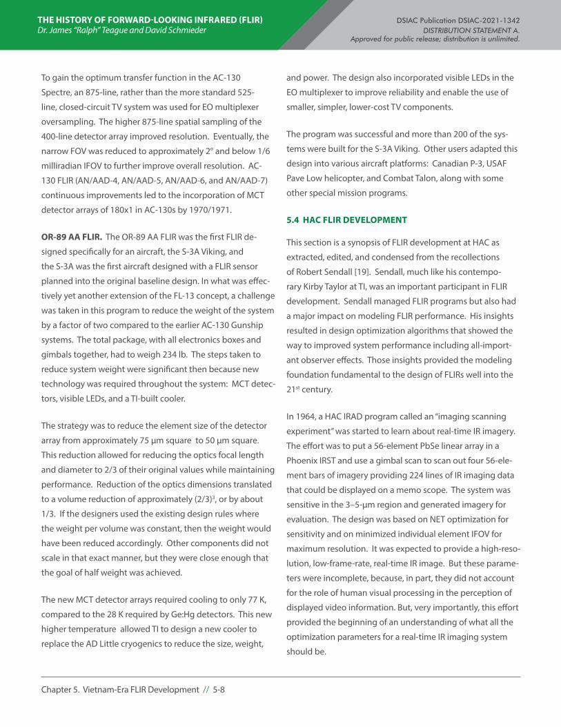
THE HISTORY OF FORWARD-LOOKING INFRARED (FLIR) DSIAC Publication DSIAC-2021-1342 Dr. James “Ralph” Teague and David Schmieder DISTRIBUTION STATEMENT A. Approved for public release; distribution is unlimited.
Chapter 5. Vietnam-Era FLIR Development // 5-8
To gain the optimum transfer function in the AC-130
Spectre, an 875-line, rather than the more standard 525-
line, closed-circuit TV system was used for EO multiplexer
oversampling. The higher 875-line spatial sampling of the
400-line detector array improved resolution. Eventually, the
narrow FOV was reduced to approximately 2° and below 1/6
milliradian IFOV to further improve overall resolution. AC-
130 FLIR (AN/AAD-4, AN/AAD-5, AN/AAD-6, and AN/AAD-7)
continuous improvements led to the incorporation of MCT
detector arrays of 180x1 in AC-130s by 1970/1971.
OR-89 AA FLIR. The OR-89 AA FLIR was the first FLIR de-
signed specifically for an aircraft, the S-3A Viking, and
the S-3A was the first aircraft designed with a FLIR sensor
planned into the original baseline design. In what was effec-
tively yet another extension of the FL-13 concept, a challenge
was taken in this program to reduce the weight of the system
by a factor of two compared to the earlier AC-130 Gunship
systems. The total package, with all electronics boxes and
gimbals together, had to weigh 234 lb. The steps taken to
reduce system weight were significant then because new
technology was required throughout the system: MCT detec-
tors, visible LEDs, and a TI-built cooler.
The strategy was to reduce the element size of the detector
array from approximately 75 µm square to 50 µm square.
This reduction allowed for reducing the optics focal length
and diameter to 2/3 of their original values while maintaining
performance. Reduction of the optics dimensions translated
to a volume reduction of approximately (2/3)3, or by about
1/3. If the designers used the existing design rules where
the weight per volume was constant, then the weight would
have been reduced accordingly. Other components did not
scale in that exact manner, but they were close enough that
the goal of half weight was achieved.
The new MCT detector arrays required cooling to only 77 K,
compared to the 28 K required by Ge:Hg detectors. This new
higher temperature allowed TI to design a new cooler to
replace the AD Little cryogenics to reduce the size, weight,
and power. The design also incorporated visible LEDs in the
EO multiplexer to improve reliability and enable the use of
smaller, simpler, lower-cost TV components.
The program was successful and more than 200 of the sys-
tems were built for the S-3A Viking. Other users adapted this
design into various aircraft platforms: Canadian P-3, USAF
Pave Low helicopter, and Combat Talon, along with some
other special mission programs.
5.4 HAC FLIR DEVELOPMENT
This section is a synopsis of FLIR development at HAC as
extracted, edited, and condensed from the recollections
of Robert Sendall [19]. Sendall, much like his contempo-
rary Kirby Taylor at TI, was an important participant in FLIR
development. Sendall managed FLIR programs but also had
a major impact on modeling FLIR performance. His insights
resulted in design optimization algorithms that showed the
way to improved system performance including all-import-
ant observer effects. Those insights provided the modeling
foundation fundamental to the design of FLIRs well into the
21st century.
In 1964, a HAC IRAD program called an “imaging scanning
experiment” was started to learn about real-time IR imagery.
The effort was to put a 56-element PbSe linear array in a
Phoenix IRST and use a gimbal scan to scan out four 56-ele-
ment bars of imagery providing 224 lines of IR imaging data
that could be displayed on a memo scope. The system was
sensitive in the 3–5-µm region and generated imagery for
evaluation. The design was based on NET optimization for
sensitivity and on minimized individual element IFOV for
maximum resolution. It was expected to provide a high-reso-
lution, low-frame-rate, real-time IR image. But these parame-
ters were incomplete, because, in part, they did not account
for the role of human visual processing in the perception of
displayed video information. But, very importantly, this effort
provided the beginning of an understanding of what all the
optimization parameters for a real-time IR imaging system
should be.

THE HISTORY OF FORWARD-LOOKING INFRARED (FLIR) DSIAC Publication DSIAC-2021-1342 Dr. James “Ralph” Teague and David Schmieder DISTRIBUTION STATEMENT A. Approved for public release; distribution is unlimited.
Chapter 5. Vietnam-Era FLIR Development // 5-9
While this system provided cosmetically pleasing images
in an observation deck “roof house” environment, it was
oversold into the Red Sea flight test program at Eglin AFB
in competition with TI. TI had built the first successful
long-wavelength FLIR by modifying a line scanner with a
scanning mirror to provide a framing system to generate a
TV-like image. Clearly, the long-wavelength TI system was
more useful for military applications in Southeast Asia. While
the TI system originally only had a single element of Ge:Hg
and a single-gun CRT, it soon went to three elements using
the three-gun structure used in color displays to enable each
detector to drive a separate gun. Even with those improve-
ments, it was clear that more detectors were needed to get
significant performance and, at least for experimentation,
TI developed a larger array and made it compatible with a
British Matricon multigun tube displaying the image.
After the Red Sea exercise, HAC applied what was learned
to the development of a high-performance, 8–11.5 µm,
real-time imaging system and also started on lower-perfor-
mance night sights using 3–5 µm technology.
Engineers assigned to this activity at HAC were well versed in
theory and mathematics. Accordingly, they recognized the
importance of cold shielding6 the detectors and the compli-
cation of the human observer as the interface. They became
familiar with the image evaluation efforts of Otto Schade, Jr.
[38], Fred Rosell [39], Coltman and Anderson [44], and others.
HAC engineering efforts led to very high-performance sys-
tems, but they were very difficult to build.
During one competitive procurement, such an optimized
HAC FLIR was engaged in a flight test versus a less optimized
Aerojet design, and it led to a major advance in future FLIR
specifications. The fact that the two systems had similar NET
and IFOV requirements, but obviously had very different
effective performance, led Lucien Biberman of IDA to form a
6 The term “cold shielding” refers to placing structured barriers around the detectors so that internal heat radiation cannot fall on the detectors and therefore reduce their sensitivity. Since all radiation exhibits quantum fluctuations, all radiation falling on the detectors increases the apparent noise output from the detectors.
committee to investigate the differences and define a new
set of performance parameters for future FLIR specifications.
At the time, NET was commonly used as the measure of sen-
sitivity, and IFOV was used to define resolution. It was clear
that these practices were not adequate and did not success-
fully optimize the HAC system.
The original committee met at IDA and was chaired by Bib-
erman, and included such well-known EO sensor experts as
John Johnson from NVL, Richard Lagault from the University
of Michigan TI, Robert Sendall from HAC, and John Jameson
from Aerojet. Robert Sendall presented the concepts of Min-
imum Resolvable Temperature (MRT), a major new concept
he originated, as well as existing metrics such as Amplitude
Transfer Function (ATF), and Modulation Transfer Function
(MTF) as three important parameters for FLIR optimization
and specification. These functions included the complete
system and the man-machine interface. The committee
changed with time but resulted in a recommended FLIR
specification document based on those originally presented
parameters. Those parameters were subsequently optimized
in the HAC Advanced FLIR (AdFLIR), which is discussed in
Section 5.4.1.
5.4.1 The Advanced FLIR (AdFLIR) for the Air Force
In 1965, the first high-performance, two-FOV FLIR was started
on IR&D funding and then was completed for the Air Force
AdFLIR 698DF contract. In this contract, HAC was competing
with Aerojet, which tried to build a similar system. The HAC
system used a staggered linear array of 176 Ge:Hg detectors
cooled to about 28 K. The elements in the array were stag-
gered to provide space for individual cold shielding of each
detector element in addition to a slot shield for the whole
array. The elements were also spaced apart so they could
be interlaced to provide 352 scan lines per frame. This array
was scanned in the horizontal and dithered in the vertical for

THE HISTORY OF FORWARD-LOOKING INFRARED (FLIR) DSIAC Publication DSIAC-2021-1342 Dr. James “Ralph” Teague and David Schmieder DISTRIBUTION STATEMENT A. Approved for public release; distribution is unlimited.
Chapter 5. Vietnam-Era FLIR Development // 5-10
interlace at the end of each field to provide an image data
rate of 60 fields per second for a frame rate of 30 frames per
second.
Two different telescopes and scanning systems were used
to provide two different FOVs depending on the position
of a field-switching mirror. The scan was provided for each
telescope by object space scanning with a pair of counter-
rotating wedge, or risley, germanium (Ge) prisms. If these
prisms were spun at constant speed, a sinusoidal scan with
minor distortion (called “dog bone”) resulted. To improve
this scan, elliptical gears were used to reduce the dog bone
as much as possible. Two other design challenges of this
scanning approach were “Narcissus” and “ghosts.” Narcissus
was the result of the prisms presenting a parallel plate of Ge
to the telescopes when the system was in the center of the
scan; the antireflection coatings on the prisms had to be of
high quality to minimize the detectors’ reflection of them-
selves as a cold object in the center of the FOV. Ghosts would
also result from imperfect antireflection lens coatings which
allowed emissions from internal structures and other parts to
reflect onto the detectors.
The array of detectors was easier to make because of the
spacing and staggering of the elements with individual
shields. This design provided effective cold shielding of these
background limited elements, which led to almost theoret-
ical sensitivity. The array and matching preamp multiplex-
ing modules were designed around the Dewar and were
mated with a cryogenic refrigerator in the sensor assembly.
While each detector had limited bandwidth, the output of
the whole detector assembly was a very wide bandwidth,
single-video signal generated by sampling and electronically
multiplexing the electrical signal of each element. Finally,
the output image from two interlaced 176 scan lines only
produced 352 display lines compared to standard displays of
the time which presented 485 active lines. So, unless this lim-
7 Sendall reported that he may be wrong about the final number of elements in the array after iterations.8 Optical exit pupils allow the placement of mechanical “stops” around the pupil to intercept internal heat emissions and prevent them from falling on the detectors. If the stops are cold, they absorb but cannot effectively re-emit.
itation was addressed, the display would appear with visible
gaps between scan lines. Accordingly, the CRT beam used
for display had to be vertically dithered at high speed to
eliminate the line-to-line gaps and thereby minimize raster
line structure.
The electronics and special display of this theoretically ideal
design were very difficult to build. When built in the original
model, this design produced a very clear image, but integrat-
ing it with aircraft was also difficult.
5.4.2 EO Vision System (EVS) FLIR for the Air Force B-52
Aircraft
Although the EVS B-52 FLIR was the result of an Army request
to equip the proposed Cheyenne attack helicopter, it sur-
prisingly ended up being the first production FLIR and was
installed on the B-52 aircraft for the Air Force in 1969. The
EVS system included both TV and FLIR systems for enhanced,
low-level penetration with improved obstacle avoidance. It
also provided the pilot with a view out of the cockpit if it had
to be closed for flash protection because of a nuclear event.
This capability made the flight safer and more effective and
provided for some target-area damage assessment. The EVS
FLIR was basically the FLIR designed for the Army’s Chey-
enne “PINE” FLIR, which had a scan converter to provide a
standard TV output. This scan converter resulted in a loss of
performance but made the helicopter integration easier and
the imagery was adequate. The FLIR design effort led to a
producible, improved FLIR based on the fundamentals of the
AdFLIR. It became the ultimate FLIR using Ge:Hg.
This FLIR had a linear array of 176 Ge:Hg elements7 with
one-element spacing between the elements so that horizon-
tally scanned fields could be interlaced to form a complete
frame of 352 lines. Cold shielding was still paramount to the
design and was accomplished using reimaging optics so that
an optical exit pupil8 could be located inside the Dewar and
THE HISTORY OF FORWARD-LOOKING INFRARED (FLIR) DSIAC Publication DSIAC-2021-1342 Dr. James “Ralph” Teague and David Schmieder DISTRIBUTION STATEMENT A. Approved for public release; distribution is unlimited.
Chapter 5. Vietnam-Era FLIR Development // 5-11
stopped with a cold stop. The optics could therefore be rath-
er slow (i.e., high f-number) and include a scanning mirror
in the converging beam to eliminate the prisms. (Scanning
generally should be done with parallel rather than converg-
ing light since the latter results in a curved image plane, but
high f-numbers mitigate the curvature.) The array was still
electronically multiplexed as it was scanned horizontally, but
now interlace was simple and, because the exit pupil was
inside the Dewar with a cold stop, there was no need to stag-
ger the detectors to allow space for individual cold shields.
These characteristics simplified the system, but the EVS FLIR
still required a special (nonstandard TV) display that could
move the CRT beam quickly in the vertical since the display
scan was fast in that direction (to keep up with vertical mul-
tiplexing) and slower in the horizontal scan direction. It also
required a good broadband video amplifier to prevent loss of
vertical MTF. The resulting display looked like a normal 2-1
TV raster scan but it was not. There were over 300 systems
originally built and, with spares, over 400.
5.4.3 The Discoid Serial Scan FLIR
Toward the end of the 1960s, HAC was looking ahead for
new design concepts besides those based on Ge:Hg. The
B-52 FLIR and others revealed the disadvantages of having a
nonstandard TV display format. In the mid-1960s, HAC was
impressed with the Swedish AGA Vision 3–5 µm imaging
system. The design was very well analyzed and built. It pro-
vided clear and uniform images, especially for a mid wave-
length system. However, it was not possible to build such a
system sensitive in the 8–11.5 µm region because the Ge:Hg
detectors did not have the necessary frequency response,
and the desired performance required a significant number
of detectors. A solution was found with the development of
new detectors.
The development of MCT detectors (discussed in Section
4.5) continued throughout the 1960s. They provided a vast
improvement over Ge:Hg detectors because they required
cooling to only 77 K instead of 28 K, offered almost any spec-
tral band out to and beyond 14 µm, and had fast temporal
response. DARPA funding continued throughout this period
although they were skeptical of eventual success. A DARPA
executive said, “HgCdTe was the detector of the future and
it always would be.” However, in the late 1960s, arrays were
being successfully produced.
HAC engineers now saw the possibility of building TV-com-
patible systems by scanning a linear array of elements over
the FOV with the elements in series rather than in parallel.
The line of elements was horizontal and was scanned in
the direction of a horizontal line. Since each detector was
looking at a different part of the scene, but all detectors
were scanning in the same direction, their outputs could be
merged by using time delay and integration (TDI). This merg-
ing resulted in improved sensitivity since the signals would
add linearly while the independent noise would only add
as the square root. Moreover, image uniformity was greatly
improved, and there was no longer any need to balance de-
tector channel outputs since all the channels were summed
together anyway. This FLIR design approach was called a “dis-
coid” design after the type of two-mirror object-space optical
scanner used to produce a raster scan at TV rates.
Because of the strongly desired standard TV output format
for many applications, HAC applied the discoid concept to
all FLIR applications. Unfortunately, the approach had many
limitations and inefficiencies. An important limitation was
the inability to add more than a few dozen detectors to the
focal plane array due to scanning geometry limitations.
Moreover, for many Army applications, a TV format provid-
ed no advantage. Indeed, the direct-viewing of scanned
LEDs, as had been used in the many experimental night
sight systems HAC built for NVL, was better suited to these
applications. Also, the possibility of using an EO multiplexor,
even with the inherent loss of performance, supported the
parallel-scanned common modules. Nevertheless, the serial
THE HISTORY OF FORWARD-LOOKING INFRARED (FLIR) DSIAC Publication DSIAC-2021-1342 Dr. James “Ralph” Teague and David Schmieder DISTRIBUTION STATEMENT A. Approved for public release; distribution is unlimited.
Chapter 5. Vietnam-Era FLIR Development // 5-12
scan system was easier to build for moderate performance
applications and was easy to make more compact. More of
the systems would have been built except for the decision to
adopt the parallel-scan common modules as the FLIR for all
government applications. While the HAC discoid FLIR design
did not become the basis for the FLIR common modules,
the concept of using TDI was ultimately adopted for second
generation (GEN2) scanning FLIRs.
5.5 SUMMARY OF VIETNAM-ERA FLIR DEVELOPMENTS
The combined demands of the Cold War and the Vietnam
War motivated the invention of FLIRs. They were needed in
the Cold War for strategic bombers to provide night vision
for both low-altitude, under-the-radar navigation and for
navigation with shuttered windshields used to prevent flash
blindness from nuclear explosions. They were needed in the
Vietnam War for night targeting of enemy ground forces. Key
prior developments in detectors, scanning systems, cryogen-
ics, electronics, and the understanding of observer impact
on system performance provided the technology for FLIRs
to emerge. However, it was the close working relationships,
sometimes contentious, among industry engineers, their
management, government organizations, and the military
users that brought it all together. These FLIRs were fledgling
devices that were custom-made and expensive. Chapter 6
discusses the ongoing relationships that initially enabled suc-
cessful FLIR development and how they were instrumental
in creating the so-called “first generation” (GEN1) FLIR, which
it actually was not, but it was the first series of FLIRs mass
produced from standard components.
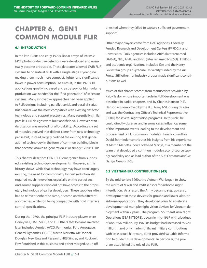
THE HISTORY OF FORWARD-LOOKING INFRARED (FLIR) DSIAC Publication DSIAC-2021-1342 Dr. James “Ralph” Teague and David Schmieder DISTRIBUTION STATEMENT A. Approved for public release; distribution is unlimited.
Chapter 6. GEN1 Common Module FLIR // 6-1
CHAPTER 6. GEN1 COMMON MODULE FLIR6.1 INTRODUCTION
In the late 1960s and early 1970s, linear arrays of intrinsic
MCT photoconductive detectors were developed and even-
tually became producible. These detectors allowed LWIR FLIR
systems to operate at 80 K with a single-stage cryoengine,
making them much more compact, lighter, and significantly
lower in power consumption. As a result, in the 1970s, IR
applications greatly increased and a strategy for high-volume
production was needed for this “first generation” of IR sensor
systems. Many innovative approaches had been applied
to FLIR designs including parallel, serial, and parallel-serial.
But parallel was the most compatible with existing detector
technology and support electronics. Many essentially similar
parallel FLIR designs were built and fielded. However, stan-
dardization was needed for affordability. Accordingly, a set
of modules evolved that did not come from new technology
per se but, instead, largely codified the existing first gener-
ation of technology in the form of common building blocks
that became known as “generation 1” or simply “GEN1” FLIRs.
This chapter describes GEN1 FLIR emergence from suppos-
edly existing technology developments. However, as this
history shows, while that technology may have been largely
existing, the need for commonality for cost reduction still
required much innovation, especially on the part of sec-
ond-source suppliers who did not have access to the propri-
etary technology of earlier developers. These suppliers often
had to reinvent either the same, or come up with different
approaches, while still being compatible with rigid interface
control specifications.
During the 1970s, the principal FLIR industry players were
Honeywell, HAC, SBRC, and TI. Others that became involved
later included Aerojet, AVCO, Fermionics, Ford Aerospace,
General Dynamics, GE, ITT, Martin Marietta, McDonnell
Douglas, New England Research, HRB Singer, and Rockwell.
Few flourished in this business and either merged, spun off,
or exited when they failed to capture sufficient government
support.
Other major players came from DoD agencies, Federally
Funded Research and Development Centers (FFRDCs), and
universities. DoD agencies included ARPA (later renamed
DARPA), NRL, AFAL, and NVL (later renamed NVESD). FFRDCs
and academic organizations included IDA and the Henry
Levinstein group at Syracuse University funded by the Air
Force. Still other nonindustry groups made significant contri-
butions as well.
Much of this chapter comes from manuscripts provided by
Kirby Taylor, whose important role in FLIR development was
described in earlier chapters, and by Charles Hanson [45].
Hanson was employed by the U.S. Army NVL during this era
and was the Contracting Officer’s Technical Representative
(COTR) for several night vision programs. In this role, he
could directly observe, and in some cases influence, some
of the important events leading to the development and
procurement of FLIR common modules. Finally, co-author
David Schmieder contributes his insights from his experience
at Martin Marietta, now Lockheed Martin, as a member of the
team that developed a common module second-source sup-
ply capability and as lead author of the FLIR Common Module
Design Manual [46].
6.2 VIETNAM-ERA CONTRIBUTIONS [45]
By the mid-to-late 1960s, the Vietnam War began to show
the worth of MWIR and LWIR sensors for airborne night
interdiction. As a result, the Army began to step up sensor
development in these devices for ground and lower-altitude
airborne applications. They developed plans to accelerate
development of multiple night vision devices for Vietnam de-
ployment within 2 years. The program, Southeast Asia Night
Operations (SEA NITEOPS), began in mid-1967 with a budget
of about $6 million. By 1968 its budget had increased to $20
million. It not only made significant military contributions
with little actual hardware, but it provided valuable informa-
tion to guide future developments. In particular, the pro-
gram established the role of the FLIR.
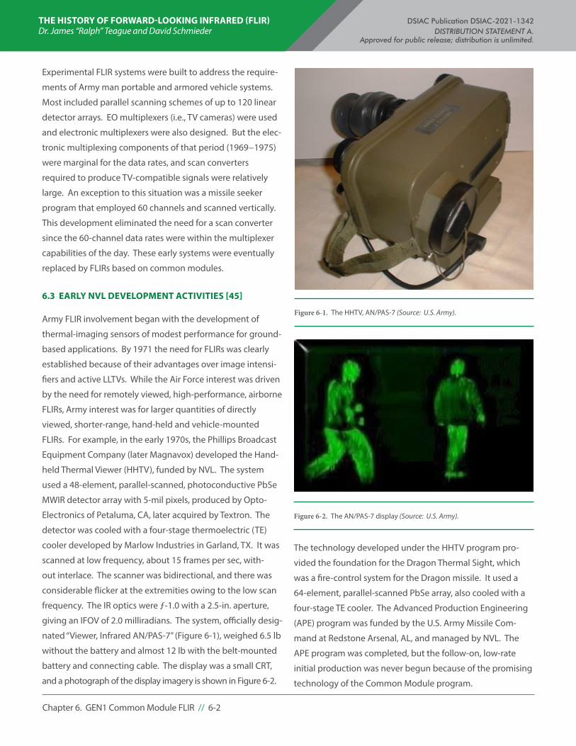
THE HISTORY OF FORWARD-LOOKING INFRARED (FLIR) DSIAC Publication DSIAC-2021-1342 Dr. James “Ralph” Teague and David Schmieder DISTRIBUTION STATEMENT A. Approved for public release; distribution is unlimited.
Chapter 6. GEN1 Common Module FLIR // 6-2
Experimental FLIR systems were built to address the require-
ments of Army man portable and armored vehicle systems.
Most included parallel scanning schemes of up to 120 linear
detector arrays. EO multiplexers (i.e., TV cameras) were used
and electronic multiplexers were also designed. But the elec-
tronic multiplexing components of that period (1969−1975)
were marginal for the data rates, and scan converters
required to produce TV-compatible signals were relatively
large. An exception to this situation was a missile seeker
program that employed 60 channels and scanned vertically.
This development eliminated the need for a scan converter
since the 60-channel data rates were within the multiplexer
capabilities of the day. These early systems were eventually
replaced by FLIRs based on common modules.
6.3 EARLY NVL DEVELOPMENT ACTIVITIES [45]
Army FLIR involvement began with the development of
thermal-imaging sensors of modest performance for ground-
based applications. By 1971 the need for FLIRs was clearly
established because of their advantages over image intensi-
fiers and active LLTVs. While the Air Force interest was driven
by the need for remotely viewed, high-performance, airborne
FLIRs, Army interest was for larger quantities of directly
viewed, shorter-range, hand-held and vehicle-mounted
FLIRs. For example, in the early 1970s, the Phillips Broadcast
Equipment Company (later Magnavox) developed the Hand-
held Thermal Viewer (HHTV), funded by NVL. The system
used a 48-element, parallel-scanned, photoconductive PbSe
MWIR detector array with 5-mil pixels, produced by Opto-
Electronics of Petaluma, CA, later acquired by Textron. The
detector was cooled with a four-stage thermoelectric (TE)
cooler developed by Marlow Industries in Garland, TX. It was
scanned at low frequency, about 15 frames per sec, with-
out interlace. The scanner was bidirectional, and there was
considerable flicker at the extremities owing to the low scan
frequency. The IR optics were ƒ-1.0 with a 2.5-in. aperture,
giving an IFOV of 2.0 milliradians. The system, officially desig-
nated “Viewer, Infrared AN/PAS-7” (Figure 6-1), weighed 6.5 lb
without the battery and almost 12 lb with the belt-mounted
battery and connecting cable. The display was a small CRT,
and a photograph of the display imagery is shown in Figure 6-2.
The technology developed under the HHTV program pro-
vided the foundation for the Dragon Thermal Sight, which
was a fire-control system for the Dragon missile. It used a
64-element, parallel-scanned PbSe array, also cooled with a
four-stage TE cooler. The Advanced Production Engineering
(APE) program was funded by the U.S. Army Missile Com-
mand at Redstone Arsenal, AL, and managed by NVL. The
APE program was completed, but the follow-on, low-rate
initial production was never begun because of the promising
technology of the Common Module program.
Figure 6-1. The HHTV, AN/PAS-7 (Source: U.S. Army).
Figure 6-2. The AN/PAS-7 display (Source: U.S. Army).
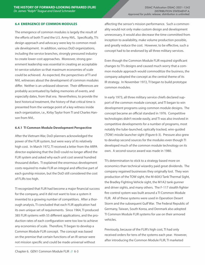
THE HISTORY OF FORWARD-LOOKING INFRARED (FLIR) DSIAC Publication DSIAC-2021-1342 Dr. James “Ralph” Teague and David Schmieder DISTRIBUTION STATEMENT A. Approved for public release; distribution is unlimited.
Chapter 6. GEN1 Common Module FLIR // 6-3
6.4 EMERGENCE OF COMMON MODULES
The emergence of common modules is largely the result of
the efforts of both TI and the U.S. Army NVL. Specifically, TI’s
design approach and advocacy were key to common mod-
ule development. In addition, various DoD organizations,
including the service branches, strongly pressured industry
to create lower-cost approaches. Moreover, strong gov-
ernment leadership was essential in creating an acceptable
tri-service solution so that maximum economies of scale
could be achieved. As expected, the perspectives of TI and
NVL witnesses about the development of common modules
differ. Neither is an unbiased observer. Their differences are
probably accentuated by fading memories of events, and
especially dates, from that era. Nevertheless, to provide the
best historical treatment, the history of that critical time is
presented from the vantage point of a key witness inside
each organization, i.e., Kirby Taylor from TI and Charles Han-
son from NVL.
6.4.1 TI Common Module Development Perspective
After the Vietnam War, DoD planners acknowledged the
power of the FLIR system, but were wary of its relatively
high cost. In March 1972, TI received a letter from the ARPA
director explaining that the DoD could no longer afford the
FLIR system and asked why each unit cost several hundred
thousand dollars. TI explained the enormous development
costs required to make FLIR an integral and effective part of
each gunship mission, but the DoD still considered the cost
of FLIRs too high.
TI recognized that FLIR had become a major financial success
for the company, and it did not want to lose a system it
invented to a growing number of competitors. After a thor-
ough analysis, TI concluded that each FLIR application had
its own unique set of requirements. Since 1964, TI produced
385 FLIR systems with 55 different applications, and the pro-
duction rates of each configuration were too low to achieve
any economies of scale. Therefore, TI began to develop a
Common Module FLIR concept. The concept was based
on the premise that certain functions of an IR sensor were
not mission specific and could be made universal without
affecting the sensor’s mission performance. Such a common-
ality would not only make custom design and development
unnecessary, it would also decrease the time committed from
inception to availability, make volume production possible,
and greatly reduce the cost. However, to be effective, such a
concept had to be endorsed by all three military services.
Even though the Common Module FLIR required significant
changes to TI’s designs and caused much worry that a com-
mon module approach would commoditize the business, the
company adopted the concept as the central theme of its
IR strategy. In November 1972, TI began to build prototype
common modules.
In early 1973, all three military service chiefs declared sup-
port of the common module concept, and TI began to win
development programs using common module designs. The
concept became an official standard in 1976. Competitive
technologies didn’t recede easily, and TI was also involved in
competitive developments for a number of programs, most
notably the tube-launched, optically tracked, wire-guided
(TOW) missile launcher sight (Figure 6-3). Pressure also grew
to develop second sources for the modules even though TI
developed much of the common module technology on its
own. A second-source award was made in 1980.
TI’s determination to stick to a strategy based more on
economics than technical wizardry paid great dividends. The
company regained businesses they originally lost. They won
production of the TOW sight, the M-60A3 Tank Thermal Sight,
the Bradley Fighting Vehicle sight, the M1A2 tank gunner
and driver sights, and many others. The F-117 stealth fighter
fire-control system was built around a TI Common Module
FLIR. All of these systems were used in Operation Desert
Storm and the subsequent Gulf War. The Federal Republic of
Germany, Taiwan, South Korea, and Denmark also adopted
TI Common Module FLIR systems for use on their armored
vehicles.
Previously, because of the FLIR’s high cost, TI had only
received orders for tens of the systems each year. However,
after introducing the Common Module FLIR, TI marketed

THE HISTORY OF FORWARD-LOOKING INFRARED (FLIR) DSIAC Publication DSIAC-2021-1342 Dr. James “Ralph” Teague and David Schmieder DISTRIBUTION STATEMENT A. Approved for public release; distribution is unlimited.
Chapter 6. GEN1 Common Module FLIR // 6-4
thousands of systems a year. As the price sharply decreased,
orders dramatically increased, and by 1998, TI had produced
more than 30,000 FLIR systems.
Many are convinced that the company’s commitment to IR
technology—even when the odds were less than favorable—
ultimately furnished the U.S. Armed Forces with a distinct
military advantage. FLIR allowed them to see through the
darkness and own the night.
6.4.2 NVL Common Module Development Perspective
NVL, like TI, also addressed the FLIR’s prohibitive costs and
formed a common module study team to find a way to sig-
nificantly reduce their cost. The NVL common module study
team developed the Universal Viewer concept to standardize
subsystems and their interfaces. TI and HAC competed to de-
fine modular concepts, develop the modular subsystems, and
build prototypical systems to demonstrate design flexibility,
performance, and maintainability.
HAC, working more independently from NVL, adopted a
novel serial-scan concept they had developed earlier. The
implementation of the HAC system was similar, conceptually,
to the FLIR shown in Figure 6-4. The concept used a row of
detectors having approximately 26 elements in the horizon-
tal direction. (Only four are illustrated in the figure.) All the
pixels in a given row scanned the same portion of the scene,
but each pixel saw a given point at a slightly different time
from the others. By appropriately delaying the signals from
the pixels using analog delay lines—a process known as
TDI—the signals could be summed to improve the signal-
to-noise ratio. While each pixel dwelt only a very short time
over a given scene point, summing the signals from a line
of pixels effectively increased the dwell time. The unidirec-
tional scan with blank retrace directly mimicked standard TV
CRT display scanning. However, it required an exceptionally
high mirror scan rate, approximately 60,000 rpm, to match
the CRT’s electron-beam scan rate, and that raised reliability
issues. However, the HAC project emphasized the elegance
of the direct interface with a CRT, as a featured part of its
cost-reduction approach.
TI’s approach was very different from that of HAC (Figure 6-5).
It included a detector array with a single vertical column of
pixels. The array was scanned horizontally at relatively low
speed with a simple mirror, which produced a unidirection-
al scan with a rapid retrace. The mirror could be vertically
dithered on alternate scans to provide for interlace to effec-
tively fill the gaps between pixels. An LED array of the same
configuration as the detector array produced a visual image
using the backside of the scan mirror. The detector came
in three configurations, 180x1, 120x1, and 60x1, to provide
options for matching performance or cost requirements. The
electronics module was modularized in the same way so that
the number of electronics channels could be matched to the
number of pixels.
Concurrently, with the development of the modules, NVL
awarded parallel contracts to TI and HAC to develop ther-
mal-imaging sights for the TOW missile. TI developed around
its modules, and HAC developed around the serial-scan ap-
proach. The HAC system produced the more pleasing image
because the process of summing all detector outputs togeth-
er eliminated detector nonuniformity effects. The elements
of the HAC TDI array were spaced far enough apart that each
pixel had its own cold shield, which made the elements more
sensitive than those in the TI parallel-scanned array where all
detectors shared one long cold shield.
Figure 6-3. TI Common Module FLIR-equipped TOW sight (Source: TI).
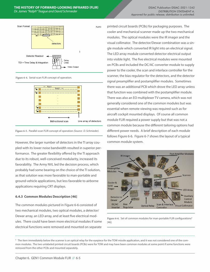
THE HISTORY OF FORWARD-LOOKING INFRARED (FLIR) DSIAC Publication DSIAC-2021-1342 Dr. James “Ralph” Teague and David Schmieder DISTRIBUTION STATEMENT A. Approved for public release; distribution is unlimited.
Chapter 6. GEN1 Common Module FLIR // 6-5
However, the larger number of detectors in the TI array cou-
pled with its lower noise bandwidth resulted in superior per-
formance. The greater flexibility offered by the TI approach
due to its robust, well-conceived modularity, increased its
favorability. The Army NVL led the decision process, which
probably had some bearing on the choice of the TI solution,
as that solution was more favorable to man-portable and
ground-vehicle applications, but less favorable to airborne
applications requiring CRT displays.
6.4.3 Common Modules Description [46]
The common modules pictured in Figure 6-6 consisted of
two mechanical modules, two optical modules, a detector/
Dewar array, an LED array, and at least five electrical mod-
ules. There could have been more electrical modules if some
electrical functions were removed and mounted on separate
9 The item immediately below the scanner is an optical relay for the eyepiece for the TOW missile application, and it was not considered one of the com-mon modules. The two unlabeled printed circuit boards (PCBs) were for TOW and may have been common modules at some point if some functions were removed from the other PCBs and mounted separately.
printed circuit boards (PCBs) for packaging purposes. The
cooler and mechanical scanner made up the two mechanical
modules. The optical modules were the IR imager and the
visual collimator. The detector/Dewar combination was a sin-
gle module which converted IR light into an electrical signal.
The LED array module converted detector electrical output
into visible light. The five electrical modules were mounted
on PCBs and included the DC/AC converter module to supply
power to the cooler, the scan and interlace controller for the
scanner, the bias regulator for the detectors, and the detector
signal preamplifier and postamplifier modules. Sometimes
there was an additional PCB which drove the LED array unless
that function was combined with the postamplifier module.
There was also an EO multiplexer TV camera, which was not
generally considered one of the common modules but was
essential when remote viewing was required such as for
aircraft cockpit mounted displays. Of course all common
module FLIR required a power supply but that was not a
common module because the different tailoring options had
different power needs. A brief description of each module
follows Figure 6-6. Figure 6-7 shows the layout of a typical
common module system.
Figure 6-6. Set of common modules for man-portable FLIR configurations9 [46].
Figure 6-4. Serial-scan FLIR concept of operation.
Figure 6-5. Parallel-scan FLIR concept of operation (Source: D. Schmieder).
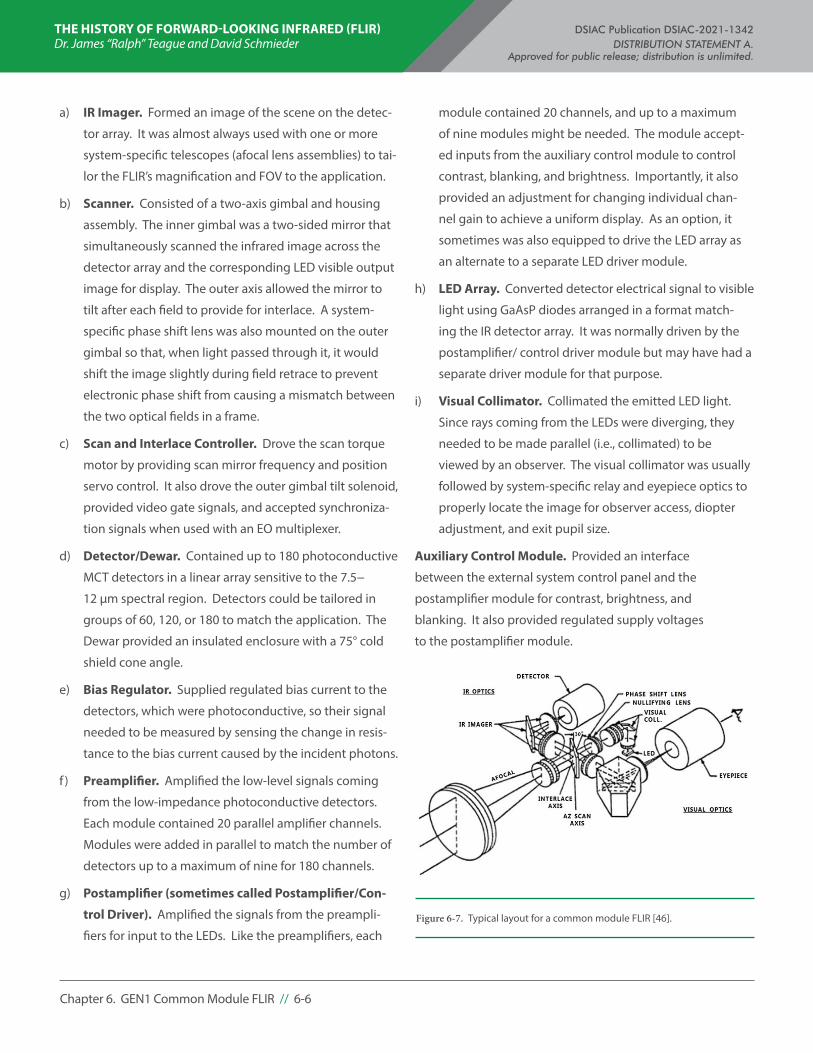
THE HISTORY OF FORWARD-LOOKING INFRARED (FLIR) DSIAC Publication DSIAC-2021-1342 Dr. James “Ralph” Teague and David Schmieder DISTRIBUTION STATEMENT A. Approved for public release; distribution is unlimited.
Chapter 6. GEN1 Common Module FLIR // 6-6
a) IR Imager. Formed an image of the scene on the detec-
tor array. It was almost always used with one or more
system-specific telescopes (afocal lens assemblies) to tai-
lor the FLIR’s magnification and FOV to the application.
b) Scanner. Consisted of a two-axis gimbal and housing
assembly. The inner gimbal was a two-sided mirror that
simultaneously scanned the infrared image across the
detector array and the corresponding LED visible output
image for display. The outer axis allowed the mirror to
tilt after each field to provide for interlace. A system-
specific phase shift lens was also mounted on the outer
gimbal so that, when light passed through it, it would
shift the image slightly during field retrace to prevent
electronic phase shift from causing a mismatch between
the two optical fields in a frame.
c) Scan and Interlace Controller. Drove the scan torque
motor by providing scan mirror frequency and position
servo control. It also drove the outer gimbal tilt solenoid,
provided video gate signals, and accepted synchroniza-
tion signals when used with an EO multiplexer.
d) Detector/Dewar. Contained up to 180 photoconductive
MCT detectors in a linear array sensitive to the 7.5−
12 µm spectral region. Detectors could be tailored in
groups of 60, 120, or 180 to match the application. The
Dewar provided an insulated enclosure with a 75° cold
shield cone angle.
e) Bias Regulator. Supplied regulated bias current to the
detectors, which were photoconductive, so their signal
needed to be measured by sensing the change in resis-
tance to the bias current caused by the incident photons.
f ) Preamplifier. Amplified the low-level signals coming
from the low-impedance photoconductive detectors.
Each module contained 20 parallel amplifier channels.
Modules were added in parallel to match the number of
detectors up to a maximum of nine for 180 channels.
g) Postamplifier (sometimes called Postamplifier/Con-
trol Driver). Amplified the signals from the preampli-
fiers for input to the LEDs. Like the preamplifiers, each
module contained 20 channels, and up to a maximum
of nine modules might be needed. The module accept-
ed inputs from the auxiliary control module to control
contrast, blanking, and brightness. Importantly, it also
provided an adjustment for changing individual chan-
nel gain to achieve a uniform display. As an option, it
sometimes was also equipped to drive the LED array as
an alternate to a separate LED driver module.
h) LED Array. Converted detector electrical signal to visible
light using GaAsP diodes arranged in a format match-
ing the IR detector array. It was normally driven by the
postamplifier/ control driver module but may have had a
separate driver module for that purpose.
i) Visual Collimator. Collimated the emitted LED light.
Since rays coming from the LEDs were diverging, they
needed to be made parallel (i.e., collimated) to be
viewed by an observer. The visual collimator was usually
followed by system-specific relay and eyepiece optics to
properly locate the image for observer access, diopter
adjustment, and exit pupil size.
Auxiliary Control Module. Provided an interface
between the external system control panel and the
postamplifier module for contrast, brightness, and
blanking. It also provided regulated supply voltages
to the postamplifier module.
Figure 6-7. Typical layout for a common module FLIR [46].
THE HISTORY OF FORWARD-LOOKING INFRARED (FLIR) DSIAC Publication DSIAC-2021-1342 Dr. James “Ralph” Teague and David Schmieder DISTRIBUTION STATEMENT A. Approved for public release; distribution is unlimited.
Chapter 6. GEN1 Common Module FLIR // 6-7
Because TI would not sell the common modules to com-
petitors, alternative sources for the FLIR common modules
submitted proposals and were awarded contracts. Martin
Marietta in Orlando, FL, received a contract for most of the
modules, including the electronics, optics, cooler, and scan-
ner. Honeywell in Lexington, MA, received a contract for the
detector arrays, and Spectronics in Richardson, TX, received a
contract for the LED array. Later, HAC developed the detector
modules and LED array, at least partially on their own. Also,
Magnavox became an alternate source for the cooler.
The availability of common modules increased the number
of suppliers of military thermal-imaging equipment. Martin
Marietta became a supplier, as did Kollsman, winning a sub-
stantial portion of the AN/TAS-4 TOW Night Sight production
business. However, TI, HAC, and Honeywell continued in the
thermal-imaging business.
Keeping the common modules “common” was a manage-
ment challenge. Although all the companies producing
modules began with the same data package, many of the
modules also contained information proprietary to TI. The
new sources had to use their own proprietary technological
expertise to manufacture such items as the detector, Dewar,
cooler, and LED array. This situation resulted in differences
among modules manufactured by the various sources.
However, at least initially, the differences were not apparent
to system developers or to end users. NVL led configuration
control.
A larger problem was the enforcement of the use of the
common modules for new system developments. On
19 June 1973 the Joint Logistics Commanders (JLC) signed
a charter to establish a Joint Technical Coordinating Group
(JTCG) for thermal-imaging systems. Its purpose was to study
tri-Service coordination of R&D, procurement, and logistics.
As a result, the JLC agreed to a tri-Service policy to use the
common modules wherever possible, with NVL having re-
sponsibility for configuration control across the services. The
charter became effective 15 July 1974. The JTCG prepared a
Joint Services Development Plan for thermal imaging, and it
included all ongoing and planned requirements.
Because common modules had been developed under the
guidance of NVL (an Army entity), there were aspects of the
modules that weren’t applicable to their use by the other
services. For example, in the use of the common modules for
airborne gimbaled systems, system requirements included
minimal weight on the gimbal, but the modules were not
designed to be separated from one another. Separation
would have allowed some components to be removed from
the gimbal thus reducing gimbal weight and size. In addi-
tion, the development of the “split-cycle” Stirling cryogenic
cooler was maturing, and that provided a better solution for
applications in which the sensor head had to fit into a small
volume. It was better because the split-cycle cooler design
removed the bulky (and vibrating) compressor stage from
the expansion valve/cold-finger so that only the latter need-
ed to be next to the detector array and on the gimbal.
Even within the Army there were difficulties. One of the dif-
ficulties was the generally understood independence of the
project managers (PMs) within the services. They had long
held to the understanding that their role was to look after the
best interests of their office and their service branch. The co-
ordination policy was in direct conflict with that long-stand-
ing practice. In addition to that, each contractor, looking for
a competitive advantage, found ways to improve upon the
original designs. There was a lot of pressure from contractors
to implement proprietary features that would secure them
future business on a given platform.
An important example of the diversification in the com-
mon modules was the XM-1 development, which led to the
M1, the Army’s main battle tank. It was developed under a
policy that gave the prime contractor full responsibility for
all subsystems. That policy was designed for enforceable
accountability, but it violated the tri-Services agreement
regarding use of the common modules. Up to this point, the
Army Materiel Command (AMC) leadership had supported

THE HISTORY OF FORWARD-LOOKING INFRARED (FLIR) DSIAC Publication DSIAC-2021-1342 Dr. James “Ralph” Teague and David Schmieder DISTRIBUTION STATEMENT A. Approved for public release; distribution is unlimited.
Chapter 6. GEN1 Common Module FLIR // 6-8
NVL in its role of configuration control, but it was AMC that
chartered the XM-1 PM to procure under the “prime contrac-
tor responsible” policy. As a result, the M1 thermal-imaging
system differed from the common modules in regard to the
detector, LED, visible collimator, bias board, and postamplifi-
er modules.
A Joint Operating Agreement and associated procedures
were drafted in 1977. The agreement designated a tri-Service
Configuration Control Board (CCB) with the Army as chair and
the Director of NVL as the Thermal Imaging System Common
Module PM. According to the agreement, each service would
have its own CCB to establish the position for that service
prior to submission of any configuration change. PMs in the
services were charged with developing procedures and for
providing representation for the tri-Service CCB. This step
required the Air Force and Navy to provide partial funding
to the Army for managing configuration control, which they
were reluctant to do, and which resulted in the new process
never being implemented. Instead, the three services con-
tinued operating under the 1974 guidelines, under which the
Director of NVL served as the configuration manager, the CCB
was an Army-only approval authority, and the Army ultimate-
ly provided only data and guidance to the PMs under the Air
Force and Navy.
NVL personnel were specifically assigned to support each
major system PM. However, NVL was not separately funded
to support configuration management, depending instead
on funding from the PMs. NVL support was generally viewed
favorably by the PMs, but the independence of prime con-
tractors conflicted with NVL’s configuration control authority.
Often change requests were submitted hurriedly because of
program schedule requirements, and justifications were inad-
equately substantiated. Delays, perceived to be bureaucratic,
were not tolerable to the PMs, some of whom were senior
military officers. There was also no preplanned product
improvement (P3I) program in place to accommodate the
progress necessary to satisfy evolving needs, although the
expanding industrial base continued to evolve the technology.
As a result of all these factors, schedule and cost concerns of
major systems overrode the configuration control process.
Nevertheless, the Common Module program and the mod-
ules themselves have to be considered a major success. Tens
of thousands of FLIR systems were delivered at costs and
production rates that could not have been realized without
the common modules. Not only was acquisition cost re-
duced, but also the cost of ownership. However, the conflict
between innovation and commonality eventually ended the
Common Module era.
6.5 COMMON MODULE DETECTOR EVOLUTION [46]
Detectors for the common modules were the most important
components of the FLIRs and the most difficult to fabricate.
The detector modules employed photoconductive linear
arrays of thin MCT sheets epoxied to sapphire carriers and
delineated into individual detector elements. After fabrica-
tion, the easier step was to mount the resulting line arrays of
60, 120, or 160 detectors onto a glass stem of a Dewar where
leads were brought to the vacuum interface/connector on
gold traces that were laser scribed on the stem. Laser-
trimmed bias resistors were located outside the Dewar to
equalize gain on the detectors across the array. The Stirling
cycle expander shaft of the cryocooler was inserted in the
hollow stem to cool the detector array to LN2 temperature.
As with many new technologies, MCT detectors were thrust
into production too early, and so a crash manufacturing tech-
nology effort was initiated to get yields to the point where
newly minted tanks and aircraft would have FLIRs to fill the
hole in the skin. Through this period, some stakeholders
continued to support extrinsic Hg technology in spite of the
significantly lower operating temperatures, with the rationale
that “MCT is the technology for the future… and always will
be” and “HCT stands for high-cost technology.” Although
MCT was a dangerous and thermodynamically unstable
material, it was an essential part of common module detector
development.
THE HISTORY OF FORWARD-LOOKING INFRARED (FLIR) DSIAC Publication DSIAC-2021-1342 Dr. James “Ralph” Teague and David Schmieder DISTRIBUTION STATEMENT A. Approved for public release; distribution is unlimited.
Chapter 6. GEN1 Common Module FLIR // 6-9
6.6 SUMMARY OF GEN1/COMMON MODULE HISTORY
The success of IR detection, first in surveillance and later in
fire control, led to a widespread demand for FLIRs and an
approach to their affordability. TI recognized from their many
customized parallel scan designs that most of the compo-
nents were similar and that standardization was not only
possible but desirable to maintain an advantageous business
posture in a competitive business. The design simplicity,
manufacturability, and elegance of the TI approach as well
as its greater sensitivity won out in a competitive procure-
ment. That procurement award decision was dominated by
field performance test results on the Army’s TOW ground-
to-ground missile guidance unit. TI was understandably
reluctant to share their technology but, in order to obtain
true cost reduction, the Army recognized there had to be
competition for the module assemblies. The Army therefore
wrote specifications for the various modules and competed
procurements. Competitors were not required to mimic TI
designs because that would have infringed on TI proprietary
information. However, they did have to meet performance,
form, and fit specifications of the TI modules in order to
qualify. The success of the Common Module program can be
attributed to both the design concept and the management
of the program.
“Mod FLIRs,” as they were sometimes called, quickly demon-
strated their worth in combat. The common module invest-
ment paid off during Operation Desert Storm, the Gulf war
fought to eject Iraqi forces from Kuwait. Mod FLIRs on front-
line weapon platforms such as the F-117 stealth bomber,
the F-15 and F-16 strike fighters, the Apache helicopter, the
M1 Abrams tank, the M2 Bradley APC, and the TOW missile
launcher played a critical role in the successful operations
against Iraq’s infrastructure and its armored and mechanized
units. The LWIR FLIRs gave U.S. pilots and gunners the edge
as they found and attacked targets not only at night, but,
because of their long wavelength obscurant penetration
capability, they also were able to attack through burning oil
clouds, battlefield smoke, and blowing sand.
It is estimated that the common modules effort brought
down the cost of scanning thermal imagers from around
$250,000 to about $50,000. TI licensed the technology to
AIM in Germany, which continued to be a supplier well past
2010. As U.S. allies and non-allied forces acquired ther-
mal-imaging capabilities, the U.S. advantage diminished.
The need to keep ahead of the threat and the emergence of
new microelectronics capabilities led to the development of
a second generation (GEN2) of FLIRs based on GEN2 detec-
tors formatted into focal-plane arrays (FPAs). Their history is
described in Chapter 7.
THE HISTORY OF FORWARD-LOOKING INFRARED (FLIR) DSIAC Publication DSIAC-2021-1342 Dr. James “Ralph” Teague and David Schmieder DISTRIBUTION STATEMENT A. Approved for public release; distribution is unlimited.
Chapter 7. GEN2 FLIR: ROIC Invention and Self-Scanned FPAs // 7-1
CHAPTER 7. GEN210 FLIR: READ-OUT INTEGRATED CIRCUIT (ROIC) INVENTION AND SELF-SCANNED FPAS7.1 INTRODUCTION11
Chapters 7, 8, and 9 address the development of GEN2 FLIRs
as follows:
• The invention of analog multiplexers called ROICs, which
are on-focal-plane analog multiplexers of multiple detec-
tor outputs. (Chapter 7).
• The development of photovoltaic MCT detector arrays
(Chapter 8).
• The mostly concurrent development of photovoltaic
InSb detector arrays and, later, uncooled microbolometer
detector arrays (Chapter 9).
In the early 1980s, Common Module FLIRs were widely
adopted in U.S. ground armor, tactical aircraft, ships, and
man-portable weapon systems. However, FLIRs were still a
novelty to the public. For instance, nightly news broadcasts
would often show the “amazing” ability of FLIR-equipped
weapon systems to see at night without relying on moon-
light, starlight, or any artificial source of illumination.
Schmieder was interviewed by an Atlanta TV station in 1980
and was asked to show their audience imagery from the new
Apache attack helicopter TADS (Target Acquisition Desig-
nation System) FLIR, which he helped design. Permission
was obtained from the Army to do so. This kind of interest
and visibility was not unusual either at home in the U.S. or in
other countries. However, to militaries around the world, it
was obvious that FLIRs were not just a novelty but were an
10 “GEN2” terminology is often used to refer specifically to the Army’s scanned linear arrays that employ GEN2 multiplexing and photovoltaic detector tech-nology, but the more expansive definition that refers to all FPAs, scanned and staring, with such technology is used in this book.11 This chapter is largely based on Georgia Institute of Technology Professional Education course notes from Infrared Technology & Applications [1].
essential tool on the modern battlefield and no military could
compete without them. It was also obvious to many that, as
with any technology, the current status of FLIRs was subject
to the inevitable changes of technological progress.
Accordingly, at least two motivational trends were develop-
ing. First, the fact that other countries could see the advan-
tage of having FLIR-enabled night operations and wanted it
for their militaries, put pressure on the United States to main-
tain its technological edge. Secondly, progress in microelec-
tronics was evolving rapidly and was impacting the design
and application of existing military and civilian electronic
devices. Moreover, they offered the possibility of introducing
whole new applications not yet envisioned. This progress put
more pressure on the U.S. to exploit it to maintain its lead in
FLIR technology. Thus, the incentive and the tools were there
for the U.S. to maintain its leadership.
FLIR technology had been paced by detector technology.
However, while continuing detector development was still
crucial to progress, GEN2 FLIR development was now also
paced by progress in microelectronics, especially in both
analog multiplexing implementations and photolithographic
feature sizes. For instance, early FLIR developers understood
the importance of adding more detectors to the focal plane
to increase sensitivity and other benefits. Increasing the
number of detectors by a factor of two means doubling the
signal, but noise doesn’t double; it only increases by the
square root of 2 because, since noise is uncorrelated, it adds
in quadrature (the square root of the sum of the squares).
Accordingly, sensitivity increases by the square root of the
number of detectors, a very significant increase. So, it was
very compelling for FLIR designers to determine how to add
as many detectors as possible to the focal plane.
Mitigating against more detectors, however, in the days of
GEN1 FLIRs with discrete detectors, was the need to add a
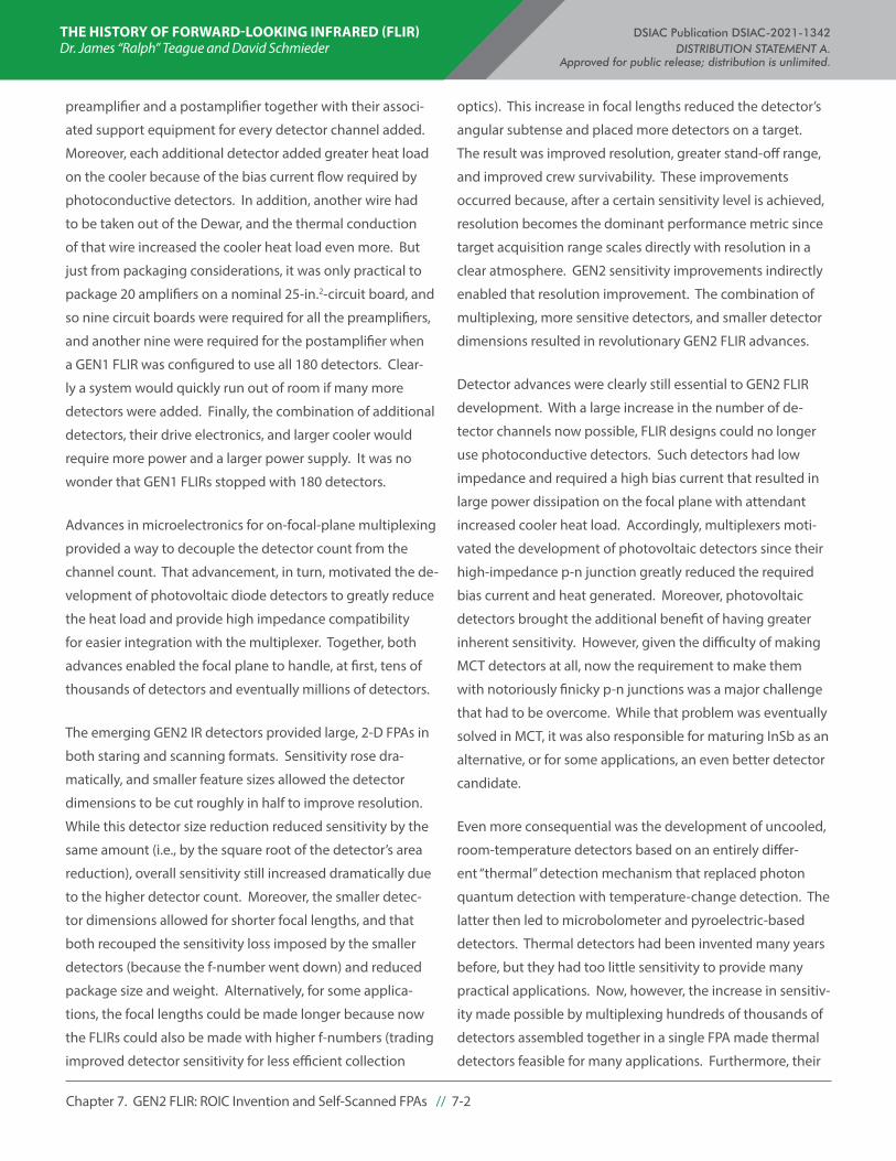
THE HISTORY OF FORWARD-LOOKING INFRARED (FLIR) DSIAC Publication DSIAC-2021-1342 Dr. James “Ralph” Teague and David Schmieder DISTRIBUTION STATEMENT A. Approved for public release; distribution is unlimited.
Chapter 7. GEN2 FLIR: ROIC Invention and Self-Scanned FPAs // 7-2
preamplifier and a postamplifier together with their associ-
ated support equipment for every detector channel added.
Moreover, each additional detector added greater heat load
on the cooler because of the bias current flow required by
photoconductive detectors. In addition, another wire had
to be taken out of the Dewar, and the thermal conduction
of that wire increased the cooler heat load even more. But
just from packaging considerations, it was only practical to
package 20 amplifiers on a nominal 25-in.2-circuit board, and
so nine circuit boards were required for all the preamplifiers,
and another nine were required for the postamplifier when
a GEN1 FLIR was configured to use all 180 detectors. Clear-
ly a system would quickly run out of room if many more
detectors were added. Finally, the combination of additional
detectors, their drive electronics, and larger cooler would
require more power and a larger power supply. It was no
wonder that GEN1 FLIRs stopped with 180 detectors.
Advances in microelectronics for on-focal-plane multiplexing
provided a way to decouple the detector count from the
channel count. That advancement, in turn, motivated the de-
velopment of photovoltaic diode detectors to greatly reduce
the heat load and provide high impedance compatibility
for easier integration with the multiplexer. Together, both
advances enabled the focal plane to handle, at first, tens of
thousands of detectors and eventually millions of detectors.
The emerging GEN2 IR detectors provided large, 2-D FPAs in
both staring and scanning formats. Sensitivity rose dra-
matically, and smaller feature sizes allowed the detector
dimensions to be cut roughly in half to improve resolution.
While this detector size reduction reduced sensitivity by the
same amount (i.e., by the square root of the detector’s area
reduction), overall sensitivity still increased dramatically due
to the higher detector count. Moreover, the smaller detec-
tor dimensions allowed for shorter focal lengths, and that
both recouped the sensitivity loss imposed by the smaller
detectors (because the f-number went down) and reduced
package size and weight. Alternatively, for some applica-
tions, the focal lengths could be made longer because now
the FLIRs could also be made with higher f-numbers (trading
improved detector sensitivity for less efficient collection
optics). This increase in focal lengths reduced the detector’s
angular subtense and placed more detectors on a target.
The result was improved resolution, greater stand-off range,
and improved crew survivability. These improvements
occurred because, after a certain sensitivity level is achieved,
resolution becomes the dominant performance metric since
target acquisition range scales directly with resolution in a
clear atmosphere. GEN2 sensitivity improvements indirectly
enabled that resolution improvement. The combination of
multiplexing, more sensitive detectors, and smaller detector
dimensions resulted in revolutionary GEN2 FLIR advances.
Detector advances were clearly still essential to GEN2 FLIR
development. With a large increase in the number of de-
tector channels now possible, FLIR designs could no longer
use photoconductive detectors. Such detectors had low
impedance and required a high bias current that resulted in
large power dissipation on the focal plane with attendant
increased cooler heat load. Accordingly, multiplexers moti-
vated the development of photovoltaic detectors since their
high-impedance p-n junction greatly reduced the required
bias current and heat generated. Moreover, photovoltaic
detectors brought the additional benefit of having greater
inherent sensitivity. However, given the difficulty of making
MCT detectors at all, now the requirement to make them
with notoriously finicky p-n junctions was a major challenge
that had to be overcome. While that problem was eventually
solved in MCT, it was also responsible for maturing InSb as an
alternative, or for some applications, an even better detector
candidate.
Even more consequential was the development of uncooled,
room-temperature detectors based on an entirely differ-
ent “thermal” detection mechanism that replaced photon
quantum detection with temperature-change detection. The
latter then led to microbolometer and pyroelectric-based
detectors. Thermal detectors had been invented many years
before, but they had too little sensitivity to provide many
practical applications. Now, however, the increase in sensitiv-
ity made possible by multiplexing hundreds of thousands of
detectors assembled together in a single FPA made thermal
detectors feasible for many applications. Furthermore, their

THE HISTORY OF FORWARD-LOOKING INFRARED (FLIR) DSIAC Publication DSIAC-2021-1342 Dr. James “Ralph” Teague and David Schmieder DISTRIBUTION STATEMENT A. Approved for public release; distribution is unlimited.
Chapter 7. GEN2 FLIR: ROIC Invention and Self-Scanned FPAs // 7-3
low cost enabled applications that were not affordable with
cooled photon detector-equipped FPAs. The remaining
sections of this chapter discuss the history of the various
approaches taken to develop focal plane multiplexers, or RO-
ICs, as they were called. But these sections also describe the
advances made in detectors to both accommodate them and
take detector technology to the next level. Together they
chronicle the GEN2 FLIR development.
7.2 SPRITE DETECTOR INVENTION
Before clock-driven analog multiplexing techniques became
the baseline approach to second-generation FPAs, a clever
approach was invented in the U.K. that arguably might have
qualified it as one of the first GEN2 devices. Since the bene-
fits of high detector count were widely appreciated, there
were various attempts to solve the detector access problem.
One of the first attempts was the use of TDI in which the
output of any given detector was delayed and summed with
the output of a following detector as described previously in
Section 5.4.3 for the HAC Discoid Serial Scan FLIR. However,
with only bulky analog electronics, delay lines, and many
discrete components, that task was difficult. Later, in the
mid-1970s, the U.K. was trying to come up with their own
version of a Common Module FLIR to duplicate the successful
U.S. Common Module FLIR program. Tom Elliot, while at the
British Defense Ministry’s Royal Radar Establishment (RRE),
Malvern, later renamed QinetiQ, realized that TDI could be ac-
complished inside a single, extended, monolithic, photocon-
ductive detector to make it appear to be many more discrete
“virtual” detectors [32, 47]. The resulting serial output could
then be coupled to a single amplifier circuit, thus effectively
multiplexing the virtual detectors together. Some called his
invention TED (for Tom Elliot’s Device), although the official
name for it was Signal Processing in the Element (SPRITE).
Figure 7-1 illustrates how it worked.
The detector’s bias voltage was chosen so that photoelec-
trons, formed from a scene pixel, drifted at the same rate
the image was being scanned. Accordingly, photo charges
accumulated and remained registered with the same scene
pixel across the whole detector. When they reached the end,
they were read out with a preamplifier. Early versions made
in 1975 were 50 µm wide by 1,000 µm long and so appeared
to make it possible to have 20 virtual detectors contained
within its length. However, charge diffusion resulted in an ef-
fective individual detector length of about 75 µm, or more, so
this approach did not achieve the same resolution in the scan
direction as was obtained by using discrete detectors. By
1980, arrays were built for parallel-serial scanning with eight
detectors each of 800 µm by 75 µm. The latter configuration
would thus effectively provide a total of about 8x10 elements
in an 80-element array while using only one preamplifier and
one postamplifier. An equivalent 80-detector U.S. GEN1 FLIR,
for example, would have needed four 20-channel pream-
plifier PCBs and four 20-channel postamplifier PCBs plus a
much larger power supply. So the U.S. GEN1 FLIR would have
required a much larger package.
SPRITE detectors were the basis of U.K. GEN1 Common Mod-
ule FLIRs, although they might have qualified as second gen-
eration. The SPRITE-based U.K. common modules provided
high sensitivity and high-quality imagery in a very compact
package. Various versions were built and, by 1999, over 3,500
FLIRs were made based on the Class II configuration alone.
They were used in the Falklands conflict and in the two Gulf
Wars.
7.3 MULTIPLEXER ROIC DESIGNS
7.3.1 Charge Coupled Device (CCD)
The invention of CCDs in the late 1960s by Smith and Boyle at
Bell Labs [48] made it possible to envision GEN2 FLIR detector
Figure 7-1. SPRITE Principle of Operation: Detected photoelectrons are made to drift at a velocity that matches the image scan rate to effectively implement TDI (Source: Elliot [32] and British Defense Ministry, RRE).

THE HISTORY OF FORWARD-LOOKING INFRARED (FLIR) DSIAC Publication DSIAC-2021-1342 Dr. James “Ralph” Teague and David Schmieder DISTRIBUTION STATEMENT A. Approved for public release; distribution is unlimited.
Chapter 7. GEN2 FLIR: ROIC Invention and Self-Scanned FPAs // 7-4
arrays which could be coupled with on-focal-plane electronic
analog signal readouts. As envisioned those readouts could
hopefully multiplex the signal from an exceptionally large
array of detectors. CCDs were easy to fabricate in silicon, and
the high purity of silicon provided high yields. Figure 7-2
illustrates their operation.
Importantly CCDs use neither photoconductive nor photo-
voltaic detectors. Instead they employ a new technique that
uses a metal-insulator-semiconductor (MIS) structure. The
MIS structure, as its name implies, is a three-layer sandwich
consisting of a metal layer on top of a silicon oxide insulator
layer, all on top of a semiconductor layer. The bottom semi-
conductor layer converts impinging photons, here incident
from the bottom, into electrons using the photoelectric
effect. This structure acts like a capacitor.
A CCD exploits the MIS structure by making the semicon-
ductor and insulator layers into a long, narrow, continuous
detector. It then covers it with a linear array of discrete metal
pad electrodes in which each pad is sequentially connected
to one of three time-varying, clock-driven voltages. This is
called a three-phase CCD and is the type shown in Figure 7-2.
Two-phase CCDs are possible as well and they only use two
clock phases connected to two pads. Clock-driven voltage
variations on the metal pads create potential wells under
the insulator, which attract the photoelectrons and form
charge packets. Each pixel site is defined by the driver pads;
thus, a single, three-phase CCD pixel consists of three metal
pads. The voltage waveforms supplied by the three-phase
clocks result in the maximum potential occurring under
only one pad, of the three, at one time. Hence, the charge
packets form only under the pad having the highest voltage
potential. This arrangement also isolates each pixel from
their adjacent pixels. However, since the clock-driven voltage
waveforms vary in time, the voltage under the second pad is
timed to exceed that under the first pad. When this happens,
the charge packet “rolls” from the first pad to under the sec-
ond pad. A repetition of this process makes the packets roll
together, unmixed, down the line of pads, for an indefinite
length and pixel count, until they are sensed at the end of the
line. The result is a sequential (serial) readout of the whole
line of charge packets.
CCDs quickly replaced film and bulky vidicons as the pre-
ferred sensor in commercial and consumer video and snap-
shot cameras. It was soon evident that CCDs could be used
to make solid-state, “self-scanned” devices that could be
useful for memory and other applications as well as imagers.
However, a major impediment for FLIR application was the
difficulty of building these devices out of the more exotic ma-
terials required to detect longer-wavelength IR photons. A
breakthrough occurred with the discovery that Shottky-Barri-
er photodiodes, made from a layer of platinum deposited on
silicon, was found to respond over the 1–5-µm region. This
discovery resulted in one of the first production GEN2 FLIRs,
when a Shottky-Barrier CCD made from platinum silicide
(PtSi) was used as the FPA for B52 bombers. These devices
were attractive because they were “monolithic,” meaning they
could be fabricated by depositing multiple material layers
sequentially on a single substrate. However, PtSi response to
MWIR photons was poor and provided a quantum efficien-
cy of only about 1%. A more exotic material would have to
be used if higher quantum efficiencies were to be attained,
but the microelectronics industry’s capital base and mate-
rial handling expertise were invested in high-purity silicon.
That capability did not easily transfer to other, lower-purity
Figure 7-2. CCD Operation (Source: Georgia Tech ITA course notes [1] as adapted from Amelio [48], 1974).

THE HISTORY OF FORWARD-LOOKING INFRARED (FLIR) DSIAC Publication DSIAC-2021-1342 Dr. James “Ralph” Teague and David Schmieder DISTRIBUTION STATEMENT A. Approved for public release; distribution is unlimited.
Chapter 7. GEN2 FLIR: ROIC Invention and Self-Scanned FPAs // 7-5
materials such as those required for IR detection. It soon
became apparent that the detectors would have to be made
separately on one type of material, but the multiplexer would
have to be made from lower-cost, higher-yielding silicon.
The combination would then have to be bonded together in
a “hybrid” configuration to form an electronically scanned IR
FPA. The multiplexer half of this device became known as an
ROIC. ROIC designs were the key to GEN2 FLIR technology.
Eventually, CCD ROICs were replaced by other types of ROICs
with better features.
7.3.2 Charge Injection Device (CID)
Another multiplexing device, the CID, was invented in the
early 1970s, shortly after the CCD. GE invented this technol-
ogy while working to design memory chips, but it was soon
adapted to imaging applications as well. Figure 7-3 illustrates
its operation. Photoelectrons accumulate in capacitive wells
formed under the intersection of each row and column. Con-
ventional shift registers are used to position a voltage at any
desired x and y location. The x location, for instance, places
that voltage at every site on the x-column of sites. Likewise,
the y-location places that voltage at every site on the y-row
of sites. Each site has an x and y pad. When not addressed,
12 The term “pedestal,” sometimes just called “background,” refers to the fact that typical scene temperatures are near 300 K, but object “signal” is the differ-ence between the object’s temperature, say 302 K, and the 300 K background. So that background temperature makes the object look like it is riding on a pedestal. Most photoelectrons in a staring detector are obviously due to the pedestal, i.e., background flux. This pedestal flux is undesirable both because it uses up most of a staring detector’s storage capacity and because that background contains quantum noise.
each pad is held at a suitable negative voltage, which allows
photo-induced charge (here positively charged carriers, or
holes) to collect under the pads. When a pad is addressed,
the negative voltage condition is canceled, and the charge
collects under the other pad. If the voltage is removed from
both wells, the charge is injected into the substrate where
it is sensed as a current or voltage change, usually by an
on-chip preamplifier. Since the particular x and y address of
each charge is known, the detected output is a “video” signal.
This technique differs from that of a CCD in that the pixels
can be accessed either sequentially as is required in a CCD or
randomly since sequential access to CID pixels is no longer
needed.
One advantage of a CID is that it can be used to “window”
smaller regions of an array to use a higher frame rate or lock
out undesired regions of an image. Another advantage is
that it mitigates blooming from bright sources because the
structure offers no ready path for excess charge to overflow
into adjacent pixels. A disadvantage of CIDs is that the cell
capacitances are all in parallel, whereas in CCDs, the capac-
itances of each cell are isolated, so Johnson noise (propor-
tional to capacitance) is much greater in a CID. However,
background shot noise is so dominant in FLIRs that the
internal noise in a CID ROIC is typically small in comparison.
Both CCDs and CIDs have the disadvantage of not being able
to use all of their surface area for charge storage since both
require empty adjacent wells to keep the pixel charges sep-
arate. This requirement reduces the maximum charge they
can store and limits their dynamic range. That is an unfortu-
nate feature of both multiplexers since large storage capacity
is required for charge storage devices when working in the IR
because the high background pedestal12 of IR scenes leaves
little room for signal storage. This limitation was overcome
by the invention of a metal-oxide-semiconductor field effect
transistor (MOSFET) switch technology, which is described in
Section 7.3.3.Figure 7-3. CID Operation (Source: Georgia Tech ITA course notes [1]).
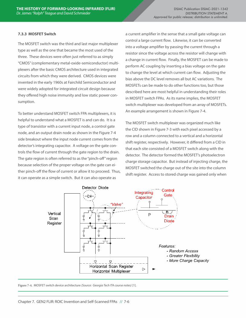
THE HISTORY OF FORWARD-LOOKING INFRARED (FLIR) DSIAC Publication DSIAC-2021-1342 Dr. James “Ralph” Teague and David Schmieder DISTRIBUTION STATEMENT A. Approved for public release; distribution is unlimited.
Chapter 7. GEN2 FLIR: ROIC Invention and Self-Scanned FPAs // 7-6
7.3.3 MOSFET Switch
The MOSFET switch was the third and last major multiplexer
type as well as the one that became the most used of the
three. These devices were often just referred to as simply
“CMOS” (complementary metal-oxide-semiconductor) multi-
plexers after the basic CMOS architecture used in integrated
circuits from which they were derived. CMOS devices were
invented in the early 1960s at Fairchild Semiconductor and
were widely adopted for integrated circuit design because
they offered high noise immunity and low static power con-
sumption.
To better understand MOSFET switch FPA multiplexers, it is
helpful to understand what a MOSFET is and can do. It is a
type of transistor with a current input node, a control gate
node, and an output drain node as shown in the Figure 7-4
side breakout where the input node current comes from the
detector’s integrating capacitor. A voltage on the gate con-
trols the flow of current through the gate region to the drain.
The gate region is often referred to as the “pinch-off” region
because selection of the proper voltage on the gate can ei-
ther pinch-off the flow of current or allow it to proceed. Thus,
it can operate as a simple switch. But it can also operate as
a current amplifier in the sense that a small gate voltage can
control a large current flow. Likewise, it can be converted
into a voltage amplifier by passing the current through a
resistor since the voltage across the resistor will change with
a change in current flow. Finally, the MOSFET can be made to
perform AC coupling by inserting a bias voltage on the gate
to change the level at which current can flow. Adjusting the
bias above the DC level removes all but AC variations. The
MOSFETs can be made to do other functions too, but those
described here are most helpful in understanding their roles
in MOSFET switch FPAs. As its name implies, the MOSFET
switch multiplexer was developed from an array of MOSFETs.
An example arrangement is shown in Figure 7-4.
The MOSFET switch multiplexer was organized much like
the CID shown in Figure 7-3 with each pixel accessed by a
row and a column connected to a vertical and a horizontal
shift register, respectively. However, it differed from a CID in
that each site consisted of a MOSFET switch along with the
detector. The detector formed the MOSFET’s photoelectron
charge storage capacitor. But instead of injecting charge, the
MOSFET switched the charge out of the site into the column
shift register. Access to stored charge was gained only when
Figure 7-4. MOSFET switch device architecture (Source: Georgia Tech ITA course notes) [1].
THE HISTORY OF FORWARD-LOOKING INFRARED (FLIR) DSIAC Publication DSIAC-2021-1342 Dr. James “Ralph” Teague and David Schmieder DISTRIBUTION STATEMENT A. Approved for public release; distribution is unlimited.
Chapter 7. GEN2 FLIR: ROIC Invention and Self-Scanned FPAs // 7-7
the gate and drain contacts were simultaneously closed by
the row and column address lines. These devices shared the
random-access feature of a CID but, unlike either CIDs or
CCDs, were able to use virtually all of the cell’s surface area
for charge storage thus doubling storage capacity. (Note
that the surface area required for MOSFET feature sizes was
so much smaller than the detector cell’s active area that
they virtually had no effect on the available surface area for
photodetection.) Moreover, the architecture was convenient
for adding more functionality to a site’s MOSFET switch such
as inserting a separate switch and access port for controlling
charge integration time so that it was independent from
the device’s frame rate. This additional functionality was an
important feature when, for instance, a FLIR needed to avoid
cell saturation in viewing warm backgrounds or by accom-
modating more efficient collection optics by using a shorter
integration time. It was also very useful when needing short
integration times to minimize image smearing with electron-
ic motion stabilization schemes. This flexibility, combined
with the wide adoption of basic CMOS fabrication by the
broader microelectronics industry, made the MOSFET switch
the preferred multiplexer for FLIR FPA ROICs.
7.4 DEVELOPMENT OF GEN2 SELF-SCANNED FPAs
The invention of ROICs resulted in the emergence of self-
scanned FPAs. ROICs were combined with detector arrays in
various ways to mate the detection function with the read-
out and multiplexing function to provide a serial output.
That output needed to be compatible not only with standard
displays but with various signal processors that worked best,
in that era, on serial information such as trackers and auto-
matic target recognizers. However, once ROICs were devel-
oped, their mating with detector arrays took different routes
that depended on the various ways to both mechanically
and electrically connect them. The challenge was to develop
detector designs that were able to solve read out compat-
ibility issues. These issues included charge storage limita-
tions with high background flux, interconnection strategies
for biasing the detectors, and signal access and grounding
circuit designs for inserting the detector signal charge into
the ROIC. Most importantly, the challenge in FPA design
included how to handle the large thermal mismatch be-
tween the more exotic materials needed to detect IR photons
with the more common materials needed to the make the
ROIC such as silicon or GaAs. The problem was the different
coefficient of thermal expansion (CTE) between detector
materials and ROIC materials, which tended to cause sepa-
ration when fabricated and stored at room temperature, but
then operated and repeatedly cycled on and off to cryogenic
temperatures. The next two chapters describe the history of
FPA development first for cooled MCT (Chapter 8) and then
for cooled InSb and other types such as room-temperature
FPAs (Chapter 9).

THE HISTORY OF FORWARD-LOOKING INFRARED (FLIR) DSIAC Publication DSIAC-2021-1342 Dr. James “Ralph” Teague and David Schmieder DISTRIBUTION STATEMENT A. Approved for public release; distribution is unlimited.
Chapter 8. GEN2 FLIRs with Cooled MCT Detectors // 8-1
CHAPTER 8. GEN2 FLIRS WITH COOLED MCT DETECTORS8.1 INTRODUCTION13
Since MCT was the leading detector material for FLIR FPA ap-
plication leading up to GEN2, it was also initially the leading
material candidate for GEN2 technology. However, InSb was
largely developed in parallel with MCT and was used in the
eventual design and fabrication of the largest formats em-
ployed in IRFPAs. While the application to InSb is the focus of
the next chapter, many comments regarding GEN2 applica-
tions to InSb are also covered in this chapter.
8.2 DEVICE STATUS IN THE EARLY 1980s
By the early 1980s, it was possible to build an amplifier-in-
tegrator in silicon and couple it with an IR detector: GE
invented the CID (later adopted at Northrop and TI) and
applied it to FPAs. HAC and TI implemented CCDs to permit
integration and multiplexing on detector arrays. The first 2-D
arrays with more than 10,000 detector elements were InSb
arrays with silicon CIDs at GE. Meanwhile, TI maintained their
totally “monolithic” MIS approach in MCT, so they fabricated
both the CCD multiplexer and the detector from MCT. That
approach put them at a temporary disadvantage in the
development of GEN2 FLIRs due to the difficulty of working
with MCT.
Among the most significant events in FPA development were
the demonstrations of the indium bump interconnect at
HAC SBRC and the via-hole interconnect at TI (also at Mullard
in the U.K.). They provided a way to connect the dissimilar
detector materials with their silicon readouts. These develop-
ments moved charge integration to the silicon multiplexers
and quickly eclipsed the capabilities of the monolithic MIS
13 This chapter is based mostly on extracts from Steve Jost’s documents written for SENSIAC by request in 2013 [20]. Jost worked for just one organization, initially GE, during this period, but that same organization was purchased and managed in succession by Sanders, Loral, LMCO, and BAE.
devices. This advantage resulted from the higher dynamic
range (well capacity) of silicon as opposed to that of MIS
capacitors made from the narrow-gap semiconductor de-
tectors. The result of this progress was the introduction of
the now widely used “hybridized” IRFPAs, which connected
silicon multiplexer arrays with dissimilar detector arrays.
Note that at a very early stage, the Air Force approached GE
in Syracuse, due to their proximity to Professor Henry Levin-
stein’s IR materials group at Syracuse University, with an offer
to become a center of excellence for IR detector technology.
GE respectfully declined, as they could see little profitability
in IR components, and so the Air Force chose HAC as the focal
point for IR development. As a result, GE lost an important
opportunity to play a larger role in IRFPA development.
The first advanced IRFPAs in limited (U.S.) production were
InSb diode hybrids from HAC SBRC. This technology was
principally developed through classified contracts from
Lockheed Space in Sunnyvale, CA, and was employed in Cold
War surveillance sensors. These early hybrid FPAs from SBRC
eventually established InSb as a detector material of choice
for Air Force and Navy longer-range airborne applications.
The InSb mid-wave response was more desirable for the Air
Force and the Navy because of improved diffraction-limited
resolution and greater atmospheric transmission. MCT’s
long-wave response was preferred by the Army since their
targets were engaged at shorter ranges but often required
greater obscurant penetration to deal with battlefield smoke
and dust.
The difficulties associated with the development and tran-
sition to production of the GEN1 Common Module family of
detectors created the impression that MCT was a high-cost
technology, and so the proposed move to second-generation
FPAs, where the detectors would be photovoltaic diodes
rather than photoconductors, was viewed with skepticism.
Ways to grow uniform, low-defect-density MCT over large
THE HISTORY OF FORWARD-LOOKING INFRARED (FLIR) DSIAC Publication DSIAC-2021-1342 Dr. James “Ralph” Teague and David Schmieder DISTRIBUTION STATEMENT A. Approved for public release; distribution is unlimited.
Chapter 8. GEN2 FLIRs with Cooled MCT Detectors // 8-2
areas, and then use it to create detector diodes, were needed
to achieve the desired performance and low cost. Solid-state
recrystallization, which had been employed for the Common
Module effort was replaced by liquid phase epitaxy (LPE).
With LPE, substrates of cadmium telluride (CdTe) or cadmium
zinc telluride (CdZnTe) were immersed in either Te-rich or Hg-
rich melts, and MCT films were precipitated out of the melt
by controlled cooling. Molecular beam epitaxy (MBE), metal
organic chemical vapor deposition (MOCVD), and isothermal
conversion were also employed. But due to the relative ma-
turity and low defect densities, LPE dominated.
8.3 MID-1980s FPA DEVELOPMENTS
As the mid-1980s approached, HAC SBRC’s double-layer
heterostructure14 diode was chosen over Honeywell’s and
Rockwell’s ion-implanted homojunction MCT diode to be-
come the LWIR detector design of choice in the United States.
TI pursued an LWIR MIS technology that was initially chosen
for the Javelin seeker and Command Launch Unit. When the
Javelin seeker contract was transferred to HAC, TI took what
they had learned from MIS and developed a competitive
alternative to the double-layer heterostructure.
In the meantime, the Navy was looking at the MWIR band,
as explained in Section 8.2, to provide improved resolution
with smaller apertures and for better atmospheric trans-
mission. MCT could be tuned to the MWIR band, but InSb
was used due to its level of maturity and significantly lower
cost. Amber Engineering cemented InSb’s dominant role in
staring technology by introducing an inexpensive ($49,999)
128x128 camera engine in the mid-1980s. Prior to this
lower-cost camera, a similar format custom MWIR FPA would
cost between $430,000 (GE InSb CID) and $1.2 M (HAC MCT).
Since that time, Amber, CE, FLIR Indigo, Santa Barbara FPA
(Figure 8-1), and HAC SBRC produced many hybrid InSb FPAs
on silicon MOSFET switches but HAC/Raytheon (Raytheon
14 A heterostructure is a combination of heterojunctions where a heterojunction is the interface between two layers of dissimilar crystalline semiconductors that have unequal band gaps. A homojunction, in contrast, has two layers of similar material with equal band gaps but has different doping. In both hetero-junction and homojunction types, the interface is formed between an n-type and a p-type semiconductor to form a p-n junction. In a double-layer hetero-structure, a narrow-bandgap material is sandwiched between two wide-bandgap layers. In the case of MCT, the narrow-gap material, needed to absorb in the LWIR, can be surrounded by wider-gap material to prevent instabilities in the weaker, narrow-gap bonds.
acquired HAC in 1997) dominated the military production of
these FPAs.
Rockwell identified substrate availability and size as the
principal cost drivers for MCT diode arrays and developed
a producible alternative to CdTe epitaxy (PACE) where they
grew modest-quality, single-crystal CdTe on sapphire by
MOCVD followed by an MWIR LPE MCT process. By going to
3-in. sapphire substrates, Rockwell probably held a tempo-
rary cost advantage over their MCT competitors but failed to
take the market away from InSb detectors, which required no
epitaxy (matching of crystalline lattice structure) and offered
similar wafer sizes. A significant investment was made in
a similar technology for LWIR diodes, PACE II, where GaAs
wafers served as the substrates, but the state of hetero-
epitaxy (growing crystals of one material on the crystal face
of another substrate material while maintaining the lattice
Figure 8-1. Several InSb FPA formats from Lockheed Martin Santa Barbara Focal Plane. Navy and Air Force staring FLIRs for targeting and navigation employed InSb FPAs in 480x640 format or larger. InSb dominated the large-format staring market with excellent performance at a reasonable cost (Source: Lockheed Martin Santa Barbara Focal Plane).
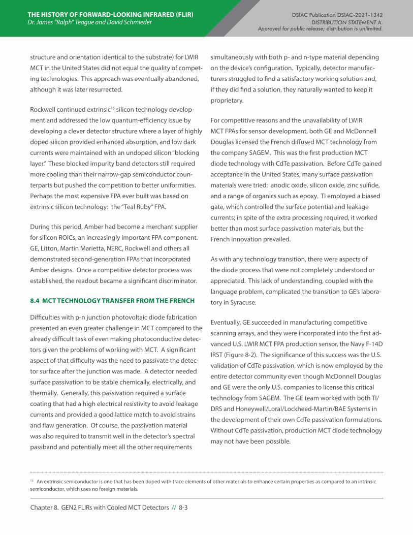
THE HISTORY OF FORWARD-LOOKING INFRARED (FLIR) DSIAC Publication DSIAC-2021-1342 Dr. James “Ralph” Teague and David Schmieder DISTRIBUTION STATEMENT A. Approved for public release; distribution is unlimited.
Chapter 8. GEN2 FLIRs with Cooled MCT Detectors // 8-3
structure and orientation identical to the substrate) for LWIR
MCT in the United States did not equal the quality of compet-
ing technologies. This approach was eventually abandoned,
although it was later resurrected.
Rockwell continued extrinsic15 silicon technology develop-
ment and addressed the low quantum-efficiency issue by
developing a clever detector structure where a layer of highly
doped silicon provided enhanced absorption, and low dark
currents were maintained with an undoped silicon “blocking
layer.” These blocked impurity band detectors still required
more cooling than their narrow-gap semiconductor coun-
terparts but pushed the competition to better uniformities.
Perhaps the most expensive FPA ever built was based on
extrinsic silicon technology: the “Teal Ruby” FPA.
During this period, Amber had become a merchant supplier
for silicon ROICs, an increasingly important FPA component.
GE, Litton, Martin Marietta, NERC, Rockwell and others all
demonstrated second-generation FPAs that incorporated
Amber designs. Once a competitive detector process was
established, the readout became a significant discriminator.
8.4 MCT TECHNOLOGY TRANSFER FROM THE FRENCH
Difficulties with p-n junction photovoltaic diode fabrication
presented an even greater challenge in MCT compared to the
already difficult task of even making photoconductive detec-
tors given the problems of working with MCT. A significant
aspect of that difficulty was the need to passivate the detec-
tor surface after the junction was made. A detector needed
surface passivation to be stable chemically, electrically, and
thermally. Generally, this passivation required a surface
coating that had a high electrical resistivity to avoid leakage
currents and provided a good lattice match to avoid strains
and flaw generation. Of course, the passivation material
was also required to transmit well in the detector’s spectral
passband and potentially meet all the other requirements
15 An extrinsic semiconductor is one that has been doped with trace elements of other materials to enhance certain properties as compared to an intrinsic semiconductor, which uses no foreign materials.
simultaneously with both p- and n-type material depending
on the device’s configuration. Typically, detector manufac-
turers struggled to find a satisfactory working solution and,
if they did find a solution, they naturally wanted to keep it
proprietary.
For competitive reasons and the unavailability of LWIR
MCT FPAs for sensor development, both GE and McDonnell
Douglas licensed the French diffused MCT technology from
the company SAGEM. This was the first production MCT
diode technology with CdTe passivation. Before CdTe gained
acceptance in the United States, many surface passivation
materials were tried: anodic oxide, silicon oxide, zinc sulfide,
and a range of organics such as epoxy. TI employed a biased
gate, which controlled the surface potential and leakage
currents; in spite of the extra processing required, it worked
better than most surface passivation materials, but the
French innovation prevailed.
As with any technology transition, there were aspects of
the diode process that were not completely understood or
appreciated. This lack of understanding, coupled with the
language problem, complicated the transition to GE’s labora-
tory in Syracuse.
Eventually, GE succeeded in manufacturing competitive
scanning arrays, and they were incorporated into the first ad-
vanced U.S. LWIR MCT FPA production sensor, the Navy F-14D
IRST (Figure 8-2). The significance of this success was the U.S.
validation of CdTe passivation, which is now employed by the
entire detector community even though McDonnell Douglas
and GE were the only U.S. companies to license this critical
technology from SAGEM. The GE team worked with both TI/
DRS and Honeywell/Loral/Lockheed-Martin/BAE Systems in
the development of their own CdTe passivation formulations.
Without CdTe passivation, production MCT diode technology
may not have been possible.
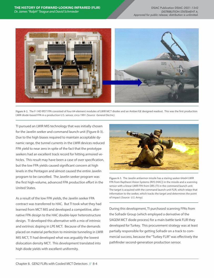
THE HISTORY OF FORWARD-LOOKING INFRARED (FLIR) DSIAC Publication DSIAC-2021-1342 Dr. James “Ralph” Teague and David Schmieder DISTRIBUTION STATEMENT A. Approved for public release; distribution is unlimited.
Chapter 8. GEN2 FLIRs with Cooled MCT Detectors // 8-4
TI pursued an LWIR MIS technology that was initially chosen
for the Javelin seeker and command launch unit (Figure 8-3).
Due to the high biases required to maintain acceptable dy-
namic range, the tunnel currents in the LWIR devices reduced
FPA yield to near zero in spite of the fact that the prototype
seekers had an excellent track record for hitting armored ve-
hicles. This result may have been a case of over specification,
but the low FPA yields caused significant concern at high
levels in the Pentagon and almost caused the entire Javelin
program to be cancelled. The Javelin seeker program was
the first high-volume, advanced FPA production effort in the
United States.
As a result of the low FPA yields, the Javelin seeker FPA
contract was transferred to HAC. But TI took what they had
learned from MCT MIS and developed a competitive, alter-
native FPA design to the HAC double-layer heterostructure
design. TI developed this alternative with a mix of intrinsic
and extrinsic doping in LPE MCT. Because of the demands
placed on material perfection to minimize tunneling in LWIR
MIS MCT, TI had developed what was arguably the lowest
dislocation density MCT. This development translated into
high diode yields with excellent uniformity.
During this development, TI purchased scanning FPAs from
the Sofradir Group (which employed a derivative of the
SAGEM MCT diode process) for a main battle tank FLIR they
developed for Turkey. This procurement strategy was at least
partially responsible for getting Sofradir on a track to com-
mercial success, because the “Turkey FLIR” was effectively the
pathfinder second-generation production sensor.
Figure 8-2. The F-14D IRST FPA consisted of four 64-element modules of LWIR MCT diodes and an Amber/GE designed readout. This was the first production LWIR diode-based FPA in a production U.S. sensor, circa 1991 (Source: General Electric).
Figure 8-3. The Javelin antiarmor missile has a staring seeker 64x64 LWIR FPA from Raytheon Vision Systems (RVS [HAC]) in the missile and a scanning sensor with a linear LWIR FPA from DRS (TI) in the command launch unit. The target is acquired with the command launch unit FLIR, which relays that information to the seeker, which tracks the target and determines the point of impact (Source: U.S. Army).
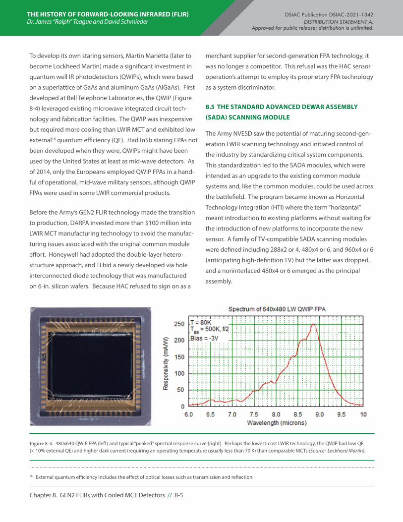
THE HISTORY OF FORWARD-LOOKING INFRARED (FLIR) DSIAC Publication DSIAC-2021-1342 Dr. James “Ralph” Teague and David Schmieder DISTRIBUTION STATEMENT A. Approved for public release; distribution is unlimited.
Chapter 8. GEN2 FLIRs with Cooled MCT Detectors // 8-5
To develop its own staring sensors, Martin Marietta (later to
become Lockheed Martin) made a significant investment in
quantum well IR photodetectors (QWIPs), which were based
on a superlattice of GaAs and aluminum GaAs (AlGaAs). First
developed at Bell Telephone Laboratories, the QWIP (Figure
8-4) leveraged existing microwave integrated circuit tech-
nology and fabrication facilities. The QWIP was inexpensive
but required more cooling than LWIR MCT and exhibited low
external16 quantum efficiency (QE). Had InSb staring FPAs not
been developed when they were, QWIPs might have been
used by the United States at least as mid-wave detectors. As
of 2014, only the Europeans employed QWIP FPAs in a hand-
ful of operational, mid-wave military sensors, although QWIP
FPAs were used in some LWIR commercial products.
Before the Army’s GEN2 FLIR technology made the transition
to production, DARPA invested more than $100 million into
LWIR MCT manufacturing technology to avoid the manufac-
turing issues associated with the original common module
effort. Honeywell had adopted the double-layer hetero-
structure approach, and TI bid a newly developed via hole
interconnected diode technology that was manufactured
on 6-in. silicon wafers. Because HAC refused to sign on as a
16 External quantum efficiency includes the effect of optical losses such as transmission and reflection.
merchant supplier for second-generation FPA technology, it
was no longer a competitor. This refusal was the HAC sensor
operation’s attempt to employ its proprietary FPA technology
as a system discriminator.
8.5 THE STANDARD ADVANCED DEWAR ASSEMBLY
(SADA) SCANNING MODULE
The Army NVESD saw the potential of maturing second-gen-
eration LWIR scanning technology and initiated control of
the industry by standardizing critical system components.
This standardization led to the SADA modules, which were
intended as an upgrade to the existing common module
systems and, like the common modules, could be used across
the battlefield. The program became known as Horizontal
Technology Integration (HTI) where the term “horizontal”
meant introduction to existing platforms without waiting for
the introduction of new platforms to incorporate the new
sensor. A family of TV-compatible SADA scanning modules
were defined including 288x2 or 4, 480x4 or 6, and 960x4 or 6
(anticipating high-definition TV) but the latter was dropped,
and a noninterlaced 480x4 or 6 emerged as the principal
assembly.
Figure 8-4. 480x640 QWIP FPA (left) and typical “peaked” spectral response curve (right). Perhaps the lowest-cost LWIR technology, the QWIP had low QE (< 10% external QE) and higher dark current (requiring an operating temperature usually less than 70 K) than comparable MCTs (Source: Lockheed Martin).
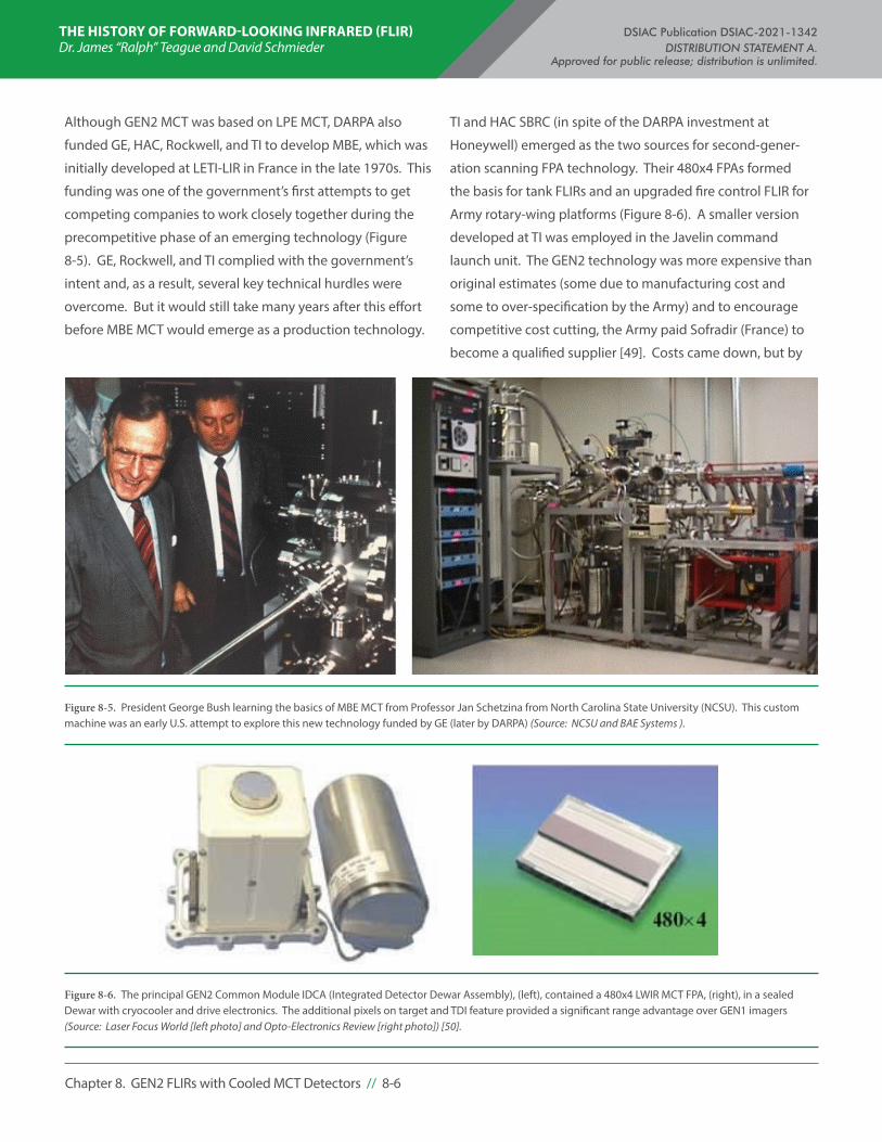
THE HISTORY OF FORWARD-LOOKING INFRARED (FLIR) DSIAC Publication DSIAC-2021-1342 Dr. James “Ralph” Teague and David Schmieder DISTRIBUTION STATEMENT A. Approved for public release; distribution is unlimited.
Chapter 8. GEN2 FLIRs with Cooled MCT Detectors // 8-6
Although GEN2 MCT was based on LPE MCT, DARPA also
funded GE, HAC, Rockwell, and TI to develop MBE, which was
initially developed at LETI-LIR in France in the late 1970s. This
funding was one of the government’s first attempts to get
competing companies to work closely together during the
precompetitive phase of an emerging technology (Figure
8-5). GE, Rockwell, and TI complied with the government’s
intent and, as a result, several key technical hurdles were
overcome. But it would still take many years after this effort
before MBE MCT would emerge as a production technology.
TI and HAC SBRC (in spite of the DARPA investment at
Honeywell) emerged as the two sources for second-gener-
ation scanning FPA technology. Their 480x4 FPAs formed
the basis for tank FLIRs and an upgraded fire control FLIR for
Army rotary-wing platforms (Figure 8-6). A smaller version
developed at TI was employed in the Javelin command
launch unit. The GEN2 technology was more expensive than
original estimates (some due to manufacturing cost and
some to over-specification by the Army) and to encourage
competitive cost cutting, the Army paid Sofradir (France) to
become a qualified supplier [49]. Costs came down, but by
Figure 8-5. President George Bush learning the basics of MBE MCT from Professor Jan Schetzina from North Carolina State University (NCSU). This custom machine was an early U.S. attempt to explore this new technology funded by GE (later by DARPA) (Source: NCSU and BAE Systems ).
Figure 8-6. The principal GEN2 Common Module IDCA (Integrated Detector Dewar Assembly), (left), contained a 480x4 LWIR MCT FPA, (right), in a sealed Dewar with cryocooler and drive electronics. The additional pixels on target and TDI feature provided a significant range advantage over GEN1 imagers (Source: Laser Focus World [left photo] and Opto-Electronics Review [right photo]) [50].
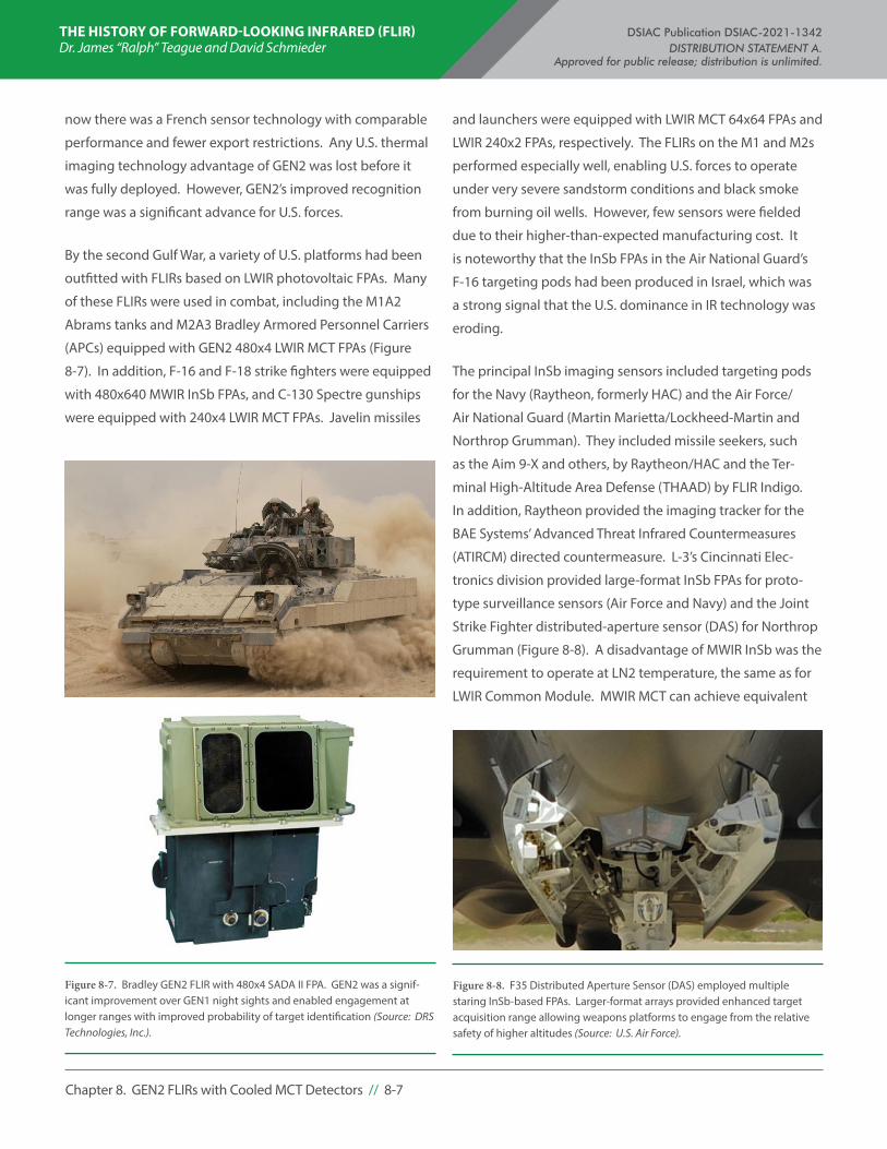
THE HISTORY OF FORWARD-LOOKING INFRARED (FLIR) DSIAC Publication DSIAC-2021-1342 Dr. James “Ralph” Teague and David Schmieder DISTRIBUTION STATEMENT A. Approved for public release; distribution is unlimited.
Chapter 8. GEN2 FLIRs with Cooled MCT Detectors // 8-7
now there was a French sensor technology with comparable
performance and fewer export restrictions. Any U.S. thermal
imaging technology advantage of GEN2 was lost before it
was fully deployed. However, GEN2’s improved recognition
range was a significant advance for U.S. forces.
By the second Gulf War, a variety of U.S. platforms had been
outfitted with FLIRs based on LWIR photovoltaic FPAs. Many
of these FLIRs were used in combat, including the M1A2
Abrams tanks and M2A3 Bradley Armored Personnel Carriers
(APCs) equipped with GEN2 480x4 LWIR MCT FPAs (Figure
8-7). In addition, F-16 and F-18 strike fighters were equipped
with 480x640 MWIR InSb FPAs, and C-130 Spectre gunships
were equipped with 240x4 LWIR MCT FPAs. Javelin missiles
and launchers were equipped with LWIR MCT 64x64 FPAs and
LWIR 240x2 FPAs, respectively. The FLIRs on the M1 and M2s
performed especially well, enabling U.S. forces to operate
under very severe sandstorm conditions and black smoke
from burning oil wells. However, few sensors were fielded
due to their higher-than-expected manufacturing cost. It
is noteworthy that the InSb FPAs in the Air National Guard’s
F-16 targeting pods had been produced in Israel, which was
a strong signal that the U.S. dominance in IR technology was
eroding.
The principal InSb imaging sensors included targeting pods
for the Navy (Raytheon, formerly HAC) and the Air Force/
Air National Guard (Martin Marietta/Lockheed-Martin and
Northrop Grumman). They included missile seekers, such
as the Aim 9-X and others, by Raytheon/HAC and the Ter-
minal High-Altitude Area Defense (THAAD) by FLIR Indigo.
In addition, Raytheon provided the imaging tracker for the
BAE Systems’ Advanced Threat Infrared Countermeasures
(ATIRCM) directed countermeasure. L-3’s Cincinnati Elec-
tronics division provided large-format InSb FPAs for proto-
type surveillance sensors (Air Force and Navy) and the Joint
Strike Fighter distributed-aperture sensor (DAS) for Northrop
Grumman (Figure 8-8). A disadvantage of MWIR InSb was the
requirement to operate at LN2 temperature, the same as for
LWIR Common Module. MWIR MCT can achieve equivalent
Figure 8-7. Bradley GEN2 FLIR with 480x4 SADA II FPA. GEN2 was a signif-icant improvement over GEN1 night sights and enabled engagement at longer ranges with improved probability of target identification (Source: DRS Technologies, Inc.).
Figure 8-8. F35 Distributed Aperture Sensor (DAS) employed multiple staring InSb-based FPAs. Larger-format arrays provided enhanced target acquisition range allowing weapons platforms to engage from the relative safety of higher altitudes (Source: U.S. Air Force).
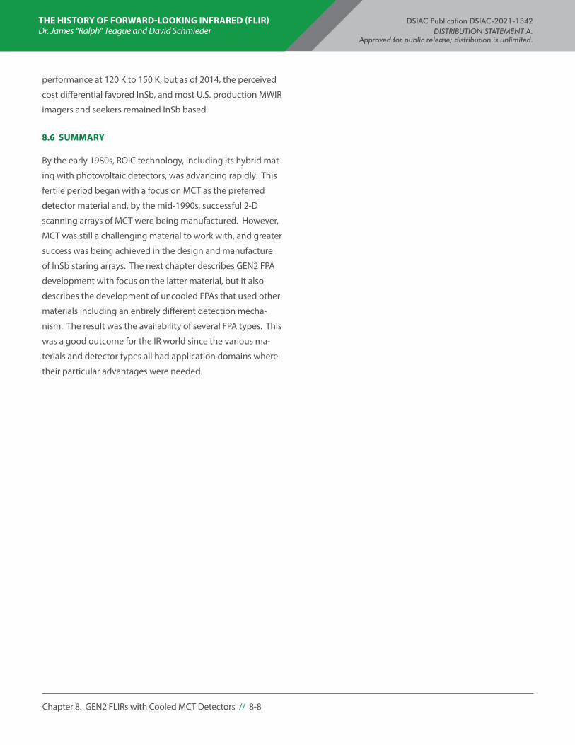
THE HISTORY OF FORWARD-LOOKING INFRARED (FLIR) DSIAC Publication DSIAC-2021-1342 Dr. James “Ralph” Teague and David Schmieder DISTRIBUTION STATEMENT A. Approved for public release; distribution is unlimited.
Chapter 8. GEN2 FLIRs with Cooled MCT Detectors // 8-8
performance at 120 K to 150 K, but as of 2014, the perceived
cost differential favored InSb, and most U.S. production MWIR
imagers and seekers remained InSb based.
8.6 SUMMARY
By the early 1980s, ROIC technology, including its hybrid mat-
ing with photovoltaic detectors, was advancing rapidly. This
fertile period began with a focus on MCT as the preferred
detector material and, by the mid-1990s, successful 2-D
scanning arrays of MCT were being manufactured. However,
MCT was still a challenging material to work with, and greater
success was being achieved in the design and manufacture
of InSb staring arrays. The next chapter describes GEN2 FPA
development with focus on the latter material, but it also
describes the development of uncooled FPAs that used other
materials including an entirely different detection mecha-
nism. The result was the availability of several FPA types. This
was a good outcome for the IR world since the various ma-
terials and detector types all had application domains where
their particular advantages were needed.
THE HISTORY OF FORWARD-LOOKING INFRARED (FLIR) DSIAC Publication DSIAC-2021-1342 Dr. James “Ralph” Teague and David Schmieder DISTRIBUTION STATEMENT A. Approved for public release; distribution is unlimited.
Chapter 9. Gen2 FLIRs with InSb and Uncooled FPAs, and System Performance Modeling Advances // 9-1
CHAPTER 9. GEN2 FLIRS WITH INSB AND UNCOOLED FPAS, AND SYSTEM PERFORMANCE MODELING ADVANCES9.1 INTRODUCTION17
The availability of indium antimonide (InSb) for detectors
enabled FLIR designs that were better optimized for airborne
ground-targeting applications. InSb enabled smaller and
lighter systems, lower costs, longer ranges in certain atmo-
spheres, and larger format FPAs. Likewise, the emergence
of uncooled, room-temperature18 FPAs had a major impact
in opening ground applications such as driver aids and rifle
scopes, but these FPAs also were well suited for small drones
and unattended sensors. Their development was remarkable
given the difficult struggle to accommodate cryocoolers in
FLIRs. But uncooled devices were ultimately the product
of GEN2 emergence since these devices would not have
achieved practical sensitivity without the invention of the
focal plane multiplexer, the key enabling technology for all
GEN2 FLIRs.
GEN2 systems also required extensive improvement to
existing models to make key design tradeoffs unique to
GEN2 FLIR characteristics. Those improvements, gained from
insights into human visual perception, allowed GEN2 FLIRs to
realize their full potential.
The development of InSb detectors was much easier than
that of MCT detectors. Section 4.5.2 described the pioneer-
17 This chapter draws from the following sources as well as other references cited in the text. Content from these sources has been heavily edited and merged by the authors.
• Excerpts from Jim Wimmers (AVCO/CE/L-3): “Document Written for SENSIAC by Request” (with photos, edits, and release approval obtained with the assistance of Mark Greiner) [51].
• Excerpts from Marion Reine (Honeywell/BAE/Infrared Detectors) with permission, “Paul W. Kruse (1927–2012), In Memoriam” [52].
18 Use of the words “uncooled” and “room-temperature” are often used interchangeably but often “uncooled” FPAs were actually cooled with small, low-pow-er thermo-electric (TE) coolers attached to the focal plane to keep them at room temperature.
ing work with InSb that led to its development by SBRC
for application in the F-14 IRST. SBRC also developed InSb
detectors for space-based sensors that, because of security,
are still largely kept from public view. Presumably, spaced-
based sensor development played a major role in maturing
InSb technology. Nevertheless, there were other major
contributors as well. Jim Wimmers, a principal founder of CE,
which later merged with L-3, lived through the period of InSb
advancement and chronicled many of the advancements
made by CE and other companies for this history. His inside
perspective, provided in this chapter, offers valuable histori-
cal insights into the emergence of InSb.
The development of uncooled FPAs is discussed following
the Wimmers-based InSb history, and the discussion re-
lies heavily on inputs from Marion Reine who was a close
colleague of Paul Kruse, the inventor of microbolometric
FPAs. Chapter 4 described Kruse’s key contributions to FLIR
development made possible by his MCT discoveries. Howev-
er, his uncooled FPAs were another breakthrough with a vast
impact on military uses but it also had civilian night vision
applications as well.
Finally, the last section describes the efforts made in FLIR
performance modeling and analysis. Many of the perfor-
mance improvements promised by GEN2 FLIR technology
were not realized when they were first invented because of
the poor understanding of how human observers process
fixed-pattern noise and by the failure of performance models
to incorporate noise traceable to the human observer’s eyes.
These model improvements were needed to fully under-
stand, exploit, and optimize the performance made possible
by GEN2 FLIR technology.
THE HISTORY OF FORWARD-LOOKING INFRARED (FLIR) DSIAC Publication DSIAC-2021-1342 Dr. James “Ralph” Teague and David Schmieder DISTRIBUTION STATEMENT A. Approved for public release; distribution is unlimited.
Chapter 9. Gen2 FLIRs with InSb and Uncooled FPAs, and System Performance Modeling Advances // 9-2
9.2 INSB FPA DEVELOPMENT [51]
9.2.1 Early InSb Detector Fabrication and Applications
Cincinnati Electronics (CE) had been involved in defense-re-
lated IR detector technology since the 1960s. At the time, it
was part of the AVCO Corporation and had a systems group
that dealt primarily in radar systems. The group’s experience
in radar sensors probably enabled it to receive a develop-
ment contract from the U.S. Air Force to investigate the feasi-
bility of using IR detectors as part of a Tail Warning System for
the F-111 Fighter/Bomber. The program eventually became
known as the Counter Measures Receiver Set and later was
given the nomenclature AAR-34. It is believed to be one of
the first major systems to use InSb detectors. It consisted of
several InSb high aspect ratio detector elements placed end-
to-end.
InSb detector fabrication was first developed in the 1960s
by Ford-Philco, but the fabrication method was considered
crude by almost any standard. An InSb boule was pulled
using the Czochralski growth method from a molten mass
of indium and antimony, with a small amount of tellurium
to make it n-type. As the boule was being pulled from the
melt, cadmium was added to the melt to make it p-type, so
that the final boule had a hemispherical dome in the middle
where the transition from n- to p-type occurred. The boule
was cut lengthwise into planks, polished and electrochemi-
cally stained to identify the p-n boundary. The plank was cut
into bars so that each had a p-n junction near the center, and
five bars were mounted side by side to produce a five-ele-
ment array.
After initially purchasing the devices from Ford-Philco, CE
brought the process in house. Then in the late 1960s, a CE
research team developed a more reliable, less labor-intensive
method of fabricating arrays using closed-ampoule gaseous
diffusion and photolithography techniques. The process was
developed by a CE research team headed by Dr. Norrn Gri,
who later worked at SBRC. Many of the processes devel-
oped are still used today in the manufacture of InSb FPAs. In
closed-ampoule gaseous diffusion, n-type wafers (cut hori-
zontally from a Czochralski-grown boule, then polished) were
sealed in a glass ampoule with a small amount of high-purity
cadmium. Elevated temperatures would evaporate the cad-
mium, creating a partial pressure of cadmium vapor in the
sealed ampoule, resulting in a highly compensated p-type
layer on top of the n-type substrate. Chemical etch-resistant
photo-resist was applied to the surface to create the desired
detector shape and size. Similarly, photolithographic tech-
niques were used to apply metal contacts to the individual
elements.
Detectors from that late 1960s era did not have a well-
defined active area. IR radiation could be absorbed
10–20 µm laterally displaced from the p-n junction itself,
and the minority carrier that was created could diffuse to the
junction and still create a photocurrent. This design gave the
appearance of a wider, lower QE detector and limited how
close detectors could be placed in an array without crosstalk
issues. The early solution to this problem was to expand the
contact pads to cover most of the semiconductor surface.
This solution created other problems in that the contact pads
could not be continuous for obvious reasons, and the gaps
between them still allowed photons to enter the detector
material. The area under the metal contact created a deple-
tion zone with very high diffusion length. Consequently,
minority carriers that previously would diffuse only
10–20 µm could move 100s of micrometers, creating signal
spurs further away than the ones the design was trying to
eliminate. Also, the added capacitance of the enlarged con-
tact pad added to the thermal (kTC, or Boltzmann’s constant
x temperature x capacitance) noise of the signal chain. Later,
another solution was devised that would benefit large-for-
mat arrays. A grounded metal layer was constructed that
covered the whole of the array, exposing only the top surface
of the p-layers, thus creating well-defined, active areas with
extremely uniform response. This was known at CE as the
buried metallization technique.
Missile Applications. A later version of the original Side-
winder Air-to-Air Missile (AIM9-L) replaced lead salt detectors
with InSb in the early 1970s. These were single-element
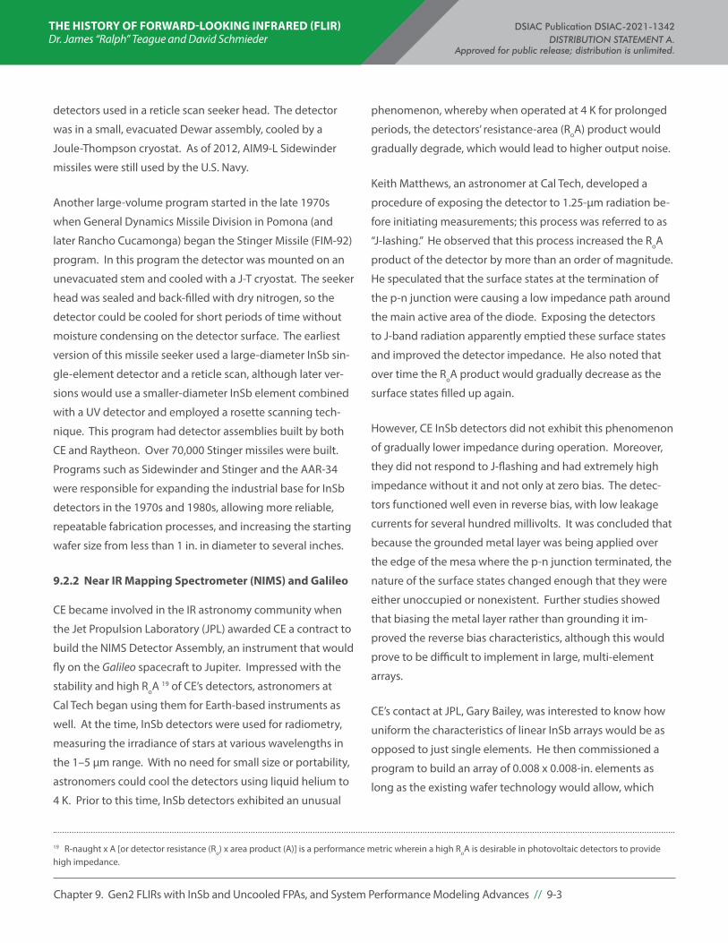
THE HISTORY OF FORWARD-LOOKING INFRARED (FLIR) DSIAC Publication DSIAC-2021-1342 Dr. James “Ralph” Teague and David Schmieder DISTRIBUTION STATEMENT A. Approved for public release; distribution is unlimited.
Chapter 9. Gen2 FLIRs with InSb and Uncooled FPAs, and System Performance Modeling Advances // 9-3
detectors used in a reticle scan seeker head. The detector
was in a small, evacuated Dewar assembly, cooled by a
Joule-Thompson cryostat. As of 2012, AIM9-L Sidewinder
missiles were still used by the U.S. Navy.
Another large-volume program started in the late 1970s
when General Dynamics Missile Division in Pomona (and
later Rancho Cucamonga) began the Stinger Missile (FIM-92)
program. In this program the detector was mounted on an
unevacuated stem and cooled with a J-T cryostat. The seeker
head was sealed and back-filled with dry nitrogen, so the
detector could be cooled for short periods of time without
moisture condensing on the detector surface. The earliest
version of this missile seeker used a large-diameter InSb sin-
gle-element detector and a reticle scan, although later ver-
sions would use a smaller-diameter InSb element combined
with a UV detector and employed a rosette scanning tech-
nique. This program had detector assemblies built by both
CE and Raytheon. Over 70,000 Stinger missiles were built.
Programs such as Sidewinder and Stinger and the AAR-34
were responsible for expanding the industrial base for InSb
detectors in the 1970s and 1980s, allowing more reliable,
repeatable fabrication processes, and increasing the starting
wafer size from less than 1 in. in diameter to several inches.
9.2.2 Near IR Mapping Spectrometer (NIMS) and Galileo
CE became involved in the IR astronomy community when
the Jet Propulsion Laboratory (JPL) awarded CE a contract to
build the NIMS Detector Assembly, an instrument that would
fly on the Galileo spacecraft to Jupiter. Impressed with the
stability and high RoA 19 of CE’s detectors, astronomers at
Cal Tech began using them for Earth-based instruments as
well. At the time, InSb detectors were used for radiometry,
measuring the irradiance of stars at various wavelengths in
the 1–5 µm range. With no need for small size or portability,
astronomers could cool the detectors using liquid helium to
4 K. Prior to this time, InSb detectors exhibited an unusual
19 R-naught x A [or detector resistance (Ro) x area product (A)] is a performance metric wherein a high RoA is desirable in photovoltaic detectors to provide high impedance.
phenomenon, whereby when operated at 4 K for prolonged
periods, the detectors’ resistance-area (RoA) product would
gradually degrade, which would lead to higher output noise.
Keith Matthews, an astronomer at Cal Tech, developed a
procedure of exposing the detector to 1.25-µm radiation be-
fore initiating measurements; this process was referred to as
“J-lashing.” He observed that this process increased the RoA
product of the detector by more than an order of magnitude.
He speculated that the surface states at the termination of
the p-n junction were causing a low impedance path around
the main active area of the diode. Exposing the detectors
to J-band radiation apparently emptied these surface states
and improved the detector impedance. He also noted that
over time the RoA product would gradually decrease as the
surface states filled up again.
However, CE InSb detectors did not exhibit this phenomenon
of gradually lower impedance during operation. Moreover,
they did not respond to J-flashing and had extremely high
impedance without it and not only at zero bias. The detec-
tors functioned well even in reverse bias, with low leakage
currents for several hundred millivolts. It was concluded that
because the grounded metal layer was being applied over
the edge of the mesa where the p-n junction terminated, the
nature of the surface states changed enough that they were
either unoccupied or nonexistent. Further studies showed
that biasing the metal layer rather than grounding it im-
proved the reverse bias characteristics, although this would
prove to be difficult to implement in large, multi-element
arrays.
CE’s contact at JPL, Gary Bailey, was interested to know how
uniform the characteristics of linear InSb arrays would be as
opposed to just single elements. He then commissioned a
program to build an array of 0.008 x 0.008-in. elements as
long as the existing wafer technology would allow, which
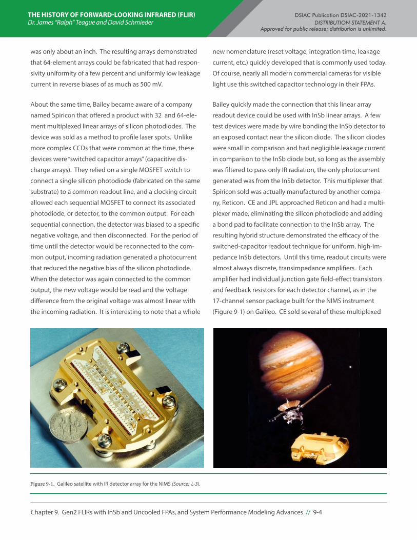
THE HISTORY OF FORWARD-LOOKING INFRARED (FLIR) DSIAC Publication DSIAC-2021-1342 Dr. James “Ralph” Teague and David Schmieder DISTRIBUTION STATEMENT A. Approved for public release; distribution is unlimited.
Chapter 9. Gen2 FLIRs with InSb and Uncooled FPAs, and System Performance Modeling Advances // 9-4
was only about an inch. The resulting arrays demonstrated
that 64-element arrays could be fabricated that had respon-
sivity uniformity of a few percent and uniformly low leakage
current in reverse biases of as much as 500 mV.
About the same time, Bailey became aware of a company
named Spiricon that offered a product with 32 and 64-ele-
ment multiplexed linear arrays of silicon photodiodes. The
device was sold as a method to profile laser spots. Unlike
more complex CCDs that were common at the time, these
devices were “switched capacitor arrays” (capacitive dis-
charge arrays). They relied on a single MOSFET switch to
connect a single silicon photodiode (fabricated on the same
substrate) to a common readout line, and a clocking circuit
allowed each sequential MOSFET to connect its associated
photodiode, or detector, to the common output. For each
sequential connection, the detector was biased to a specific
negative voltage, and then disconnected. For the period of
time until the detector would be reconnected to the com-
mon output, incoming radiation generated a photocurrent
that reduced the negative bias of the silicon photodiode.
When the detector was again connected to the common
output, the new voltage would be read and the voltage
difference from the original voltage was almost linear with
the incoming radiation. It is interesting to note that a whole
new nomenclature (reset voltage, integration time, leakage
current, etc.) quickly developed that is commonly used today.
Of course, nearly all modern commercial cameras for visible
light use this switched capacitor technology in their FPAs.
Bailey quickly made the connection that this linear array
readout device could be used with InSb linear arrays. A few
test devices were made by wire bonding the InSb detector to
an exposed contact near the silicon diode. The silicon diodes
were small in comparison and had negligible leakage current
in comparison to the InSb diode but, so long as the assembly
was filtered to pass only IR radiation, the only photocurrent
generated was from the InSb detector. This multiplexer that
Spiricon sold was actually manufactured by another compa-
ny, Reticon. CE and JPL approached Reticon and had a multi-
plexer made, eliminating the silicon photodiode and adding
a bond pad to facilitate connection to the InSb array. The
resulting hybrid structure demonstrated the efficacy of the
switched-capacitor readout technique for uniform, high-im-
pedance InSb detectors. Until this time, readout circuits were
almost always discrete, transimpedance amplifiers. Each
amplifier had individual junction gate field-effect transistors
and feedback resistors for each detector channel, as in the
17-channel sensor package built for the NIMS instrument
(Figure 9-1) on Galileo. CE sold several of these multiplexed
Figure 9-1. Galileo satellite with IR detector array for the NIMS (Source: L-3).
THE HISTORY OF FORWARD-LOOKING INFRARED (FLIR) DSIAC Publication DSIAC-2021-1342 Dr. James “Ralph” Teague and David Schmieder DISTRIBUTION STATEMENT A. Approved for public release; distribution is unlimited.
Chapter 9. Gen2 FLIRs with InSb and Uncooled FPAs, and System Performance Modeling Advances // 9-5
linear array devices as a standard product primarily for as-
tronomy applications, and used the nomenclature integrated
multiplexed hybrid (IMH) array or IMH-32, IMH 64, and IMH-
128. JPL also contracted CE to build a 512-element switched
capacitor array as the sensor package for the visible/IR map-
ping spectrometer (VIMS) instrument (Figure 9-2) that flew
on the Cassini spacecraft that went into orbit around Saturn.
The commercial viability of these linear array devices was
short-lived, as the age of 2-D staring arrays was now begin-
ning. Nevertheless, the demonstration of a direct input,
switched capacitor technique would prove critical to CE’s
later successes.
By the late 1980s, a few of the larger companies (Rockwell,
HAC SBRC, TI) began producing the first 2-D arrays. Several
key technologies were required to build an array, and only
this small group had the internal sources for these tech-
nologies. The capital equipment requirements were also
prohibitive to small companies or small groups within larger
companies. The most important element was a source for
2-D silicon multiplexers. Each of these three companies had
internal silicon integrated circuit (IC) foundries (and in-house
IC designers) that could develop and build the multiplexer.
Of course, each company had a detector capability as well,
primarily MCT, since most military FLIRS were made of long
wave MCT. Bump bonders were commercially available
since they were being used in flip chip ICs, but they cost
several hundred thousand dollars each. Similarly, arrays,
once bump bonded, had to be thinned to a thickness on the
order of 10 µm, so photons would not create carriers too far
away from the p-n junction area, lest they recombine before
being swept across the junction. The only available thinning
technique at the time was diamond turning, and diamond
turning systems cost between $500,000 and $1 million. The
combined cost of those two systems alone was three to four
times more than the annual capital budget of CE’s detector
group (CE’s main line of business at the time was still military
communications). CE had made inquiries to several of the
major defense companies, but for obvious reasons they were
unwilling to sell multiplexers to companies they viewed as
competitors. CE did not see a pathway to participating in this
new technology.
For several years, these companies dominated the 2-D IR
industry. For the most part, the devices being developed
were mid-wave and long-wave MCT arrays, since the fund-
ing source was primarily the U.S. Army. The conventional
wisdom at the time was that mid-wave MCT could eventually
be made to operate at high enough temperatures so that a
cryocooler would not be required. SBRC made an InSb array,
but its intended market for that device was IR astronomy
and was operated at liquid helium temperatures (4 K). Then
several events led to CE’s entrance into the market:
1. The understanding of the importance of spatial noise.
2. The growth of a “cottage industry” of self-employed IC multiplexer designers.
3. The establishment of stand-alone silicon foundries.
4. The development of a novel front side illuminated array that did not require diamond turning as a thinning technique.
5. The availability of miniature, low-power cryocoolers.
Figure 9-2. Multiplexed InSb detector array for the VIMS (Source: L-3).
THE HISTORY OF FORWARD-LOOKING INFRARED (FLIR) DSIAC Publication DSIAC-2021-1342 Dr. James “Ralph” Teague and David Schmieder DISTRIBUTION STATEMENT A. Approved for public release; distribution is unlimited.
Chapter 9. Gen2 FLIRs with InSb and Uncooled FPAs, and System Performance Modeling Advances // 9-6
9.2.3 Spatial Noise
Most of the technical conferences at the time were dominat-
ed by the major companies (Rockwell, HAC SBRC, TI), and the
focus was primarily on improved sensitivity, measured by
detectivity, or D-star (D*). This was the common method of
determining the quality of single-element and linear arrays.
For at least a year, the performance of 2-D FPAs was shown
at these conferences as a histogram of the individual D* of
each element. The quality of an array was represented by
measurements such as the average D* and the minimum
D* of 99% of all the elements. A few static images might be
shown, but it would be a few years before real-time video
processing would make video possible. For unlike silicon im-
aging arrays whose signal variation from element to element
was less than a percent, the responsivity and offset values of
each individual element in an IR array varied significantly and
required each element to be corrected with a unique gain
and unique offset value. There were no processors that could
do this in real-time.
A group from Hanscom AFB, led by Dr. Freeman Shepard,
had been working on an alternative technology—platinum
silicide (PtSi). Their approach was to fabricate a PtSi Schottky
barrier diode directly on the surface of the silicon multiplexer.
The resulting structure produced an array with high opera-
bility and excellent uniformity, but with only ~1% quantum
efficiency. It also eliminated the need for bump bonding
and hybrid structures. So, while the MCT companies were
reporting D* values of 10E10 and 10E11, Shepard’s group
was showing only 10E8 and 10E9. Many competing groups
did not consider the work competitive, and in some cases, it
was derided. It was not until real-time imagery of higher D*
arrays was available and began to be reported that the real
value of Shepard’s approach was understood.
Wimmers [51] remembered the stunned silence in the room
when the first PtSi video images were shown at an IRIS
conference. Because of the purity of Si available for Si-based
Schottky diodes, responsivity and dark current were excep-
tionally uniform and remained uniform over FPA operating
temperature variations as well. Clearly objects could be
detected with the low-sensitivity PtSi array that could not be
seen in MCT arrays with sensitivities sometimes two orders
of magnitude greater. Normally the variation in signal of a
single detector due to its electrical noise could be expressed
as how much of a temperature difference in the scene would
be required to produce the same signal amplitude. That
metric became the standard noise equivalent temperature
difference (NETD). Now it quickly became understood that a
new method of determining the quality of an imaging array
would be necessary. The “spatial noise” or variation in gain
or offset between each element of an array was as important
to consider as the electrical noise of each individual element.
The new metric that would be used would be the “spatial
noise equivalent temperature difference” or spatial NETD.
Consequently, NETD due to individual detector/readout
circuit noise was added in quadrature to the nonuniformi-
ty-based spatial NETD to result in a total NETD of the FPA.
It was then easy to understand why the PtSi FPA imagery
looked better than its MCT-based counterparts of the time.
While the early MCT FPAs had very low detector-based NETD,
that NETD was overwhelmed by the high spatial NETD due
to nonlinear gain and gain drift with operating temperature.
On the other hand, PtSi arrays had very low spatial NETD, and
were limited instead by their detector NETD, which was lower
than the spatial NETD of the MCT FPAs.
After array nonuniformity effects started to be understood,
nonuniformity “correction” techniques began to be applied.
One of the first techniques used to correct arrays was to place
a uniform, low-signal source in front of the array, record the
signal of each element, and repeat using a uniform, high-sig-
nal source. (In some cases, it was as rudimentary as using
white and black pieces of cardboard.) The measured values
for slope and offset were the equivalent of gain and bright-
ness, and two corresponding constants for each element
could be stored in memory and used to correct the output
as each element was read out of the array. This process was
referred to as a “two-point correction,” as illustrated in Figure
9-3. While it eliminated the vast majority of the nonunifor-
mities in the images, it had several limitations. Most impor-
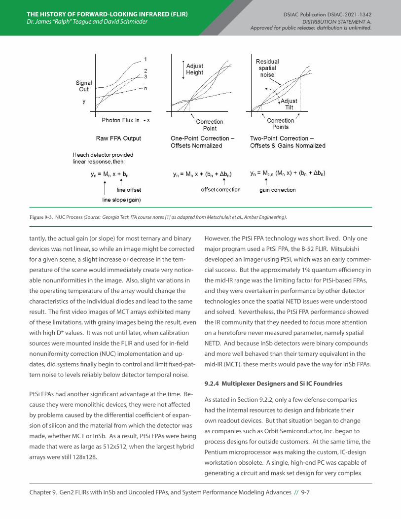
THE HISTORY OF FORWARD-LOOKING INFRARED (FLIR) DSIAC Publication DSIAC-2021-1342 Dr. James “Ralph” Teague and David Schmieder DISTRIBUTION STATEMENT A. Approved for public release; distribution is unlimited.
Chapter 9. Gen2 FLIRs with InSb and Uncooled FPAs, and System Performance Modeling Advances // 9-7
tantly, the actual gain (or slope) for most ternary and binary
devices was not linear, so while an image might be corrected
for a given scene, a slight increase or decrease in the tem-
perature of the scene would immediately create very notice-
able nonuniformities in the image. Also, slight variations in
the operating temperature of the array would change the
characteristics of the individual diodes and lead to the same
result. The first video images of MCT arrays exhibited many
of these limitations, with grainy images being the result, even
with high D* values. It was not until later, when calibration
sources were mounted inside the FLIR and used for in-field
nonuniformity correction (NUC) implementation and up-
dates, did systems finally begin to control and limit fixed-pat-
tern noise to levels reliably below detector temporal noise.
PtSi FPAs had another significant advantage at the time. Be-
cause they were monolithic devices, they were not affected
by problems caused by the differential coefficient of expan-
sion of silicon and the material from which the detector was
made, whether MCT or InSb. As a result, PtSi FPAs were being
made that were as large as 512x512, when the largest hybrid
arrays were still 128x128.
However, the PtSi FPA technology was short lived. Only one
major program used a PtSi FPA, the B-52 FLIR. Mitsubishi
developed an imager using PtSi, which was an early commer-
cial success. But the approximately 1% quantum efficiency in
the mid-IR range was the limiting factor for PtSi-based FPAs,
and they were overtaken in performance by other detector
technologies once the spatial NETD issues were understood
and solved. Nevertheless, the PtSi FPA performance showed
the IR community that they needed to focus more attention
on a heretofore never measured parameter, namely spatial
NETD. And because InSb detectors were binary compounds
and more well behaved than their ternary equivalent in the
mid-IR (MCT), these merits would pave the way for InSb FPAs.
9.2.4 Multiplexer Designers and Si IC Foundries
As stated in Section 9.2.2, only a few defense companies
had the internal resources to design and fabricate their
own readout devices. But that situation began to change
as companies such as Orbit Semiconductor, Inc. began to
process designs for outside customers. At the same time, the
Pentium microprocessor was making the custom, IC-design
workstation obsolete. A single, high-end PC was capable of
generating a circuit and mask set design for very complex
Figure 9-3. NUC Process (Source: Georgia Tech ITA course notes [1] as adapted from Metschuleit et al., Amber Engineering).
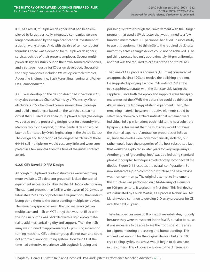
THE HISTORY OF FORWARD-LOOKING INFRARED (FLIR) DSIAC Publication DSIAC-2021-1342 Dr. James “Ralph” Teague and David Schmieder DISTRIBUTION STATEMENT A. Approved for public release; distribution is unlimited.
Chapter 9. Gen2 FLIRs with InSb and Uncooled FPAs, and System Performance Modeling Advances // 9-8
ICs. As a result, multiplexer designers that had been em-
ployed by larger, vertically integrated companies were no
longer constrained by the significant capital investment of
a design workstation. And, with the rise of semiconductor
foundries, there was a demand for multiplexer designers’
services outside of their present employer. Several multi-
plexer designers struck out on their own, formed companies,
and a cottage industry for IC design developed. Several of
the early companies included Walmsley Microelectronics,
Augustine Engineering, Black Forest Engineering, and Valley
Oak Semiconductor.
As CE was developing the design described in Section 9.2.5,
they also contacted Charles Walmsley of Walmsley Micro-
electronics in Scotland and commissioned him to design
and build a multiplexer based on the switched capacitor
circuit that CE used in its linear multiplexed arrays (the design
was based on the processing design rules for a foundry in a
Marconi facility in England, but the identical design would
later be fabricated by Orbit Engineering in the United States).
The design and fabrication of the original batch run of these
64x64-cell multiplexers would cost very little and were com-
pleted in a few months from the time of the initial contract
award.
9.2.5 CE’s Novel 2-D FPA Design
Although multiplexed readout structures were becoming
more available, CE’s detector group still lacked the capital
equipment necessary to fabricate the 2-D InSb detector array.
The standard process then (still in wide use as of 2012) was to
fabricate a 2-D array of photosensitive junctions, then indium
bump bond them to the corresponding multiplexer device.
The remaining space between the two materials (silicon
multiplexer and InSb or MCT array) that was not filled with
the indium bumps was backfilled with a rigid epoxy mate-
rial to add mechanical rigidity and support. Then the InSb
array was thinned to approximately 15 µm using a diamond
turning machine. CE’s detector group did not own and could
not afford a diamond turning system. However, CE at the
time had extensive experience with Logitech lapping and
polishing systems through their involvement with the Stinger
program that used a UV detector that was thinned to a few
hundred micrometers. CE personnel had tried unsuccessfully
to use this equipment to thin InSb to the required thickness;
uniformity across a single device could not be achieved. (The
polishing process had only approximately 10-µm uniformity,
and that was the required thickness of the end structure.)
Then one of CE’s process engineers (Al Timlin) conceived of
an approach, circa 1993, to resolve the polishing problem.
He suggested epoxying a whole InSb wafer of 2-D arrays
to a sapphire substrate, with the detector side facing the
sapphire. Since both the epoxy and sapphire were transpar-
ent to most of the MWIR, the other side could be thinned to
40 µm using the lapping/polishing equipment. Then, the
remaining material between the active elements could be
selectively chemically etched, until all that remained were
individual InSb p-n junctions each held to the host substrate
by epoxy. (This meant that the InSb array would not have
the thermal expansion/contraction properties of InSb at
all, since the diodes were now mechanically isolated, but
rather would have the properties of the host substrate, a fact
that would be exploited in later years for very large arrays.)
Another grid of “grounding lines” was applied using standard
photolithographic techniques to electrically reconnect all the
diodes. Figure 9-4 illustrates the overall configuration. So
now instead of a p-on-common-n structure, the new device
was n-on-common-p. The original attempt to implement
this structure was performed on a 64x64 array of elements
on 100-µm centers. It worked the first time. This first device
was fabricated by Chuck Martin, a CE process technician. Mr.
Martin would continue to develop 2-D array processes for CE
over the next 25 years.
These first devices were built on sapphire substrates, not only
because they were transparent in the MWIR, but also because
it was necessary to be able to see the front side of the array
for alignment during processing and bump bonding. This
worked well enough for the original devices, but after 100
cryo cooling cycles, the arrays would begin to delaminate
in the corners. This of course was due to the difference in
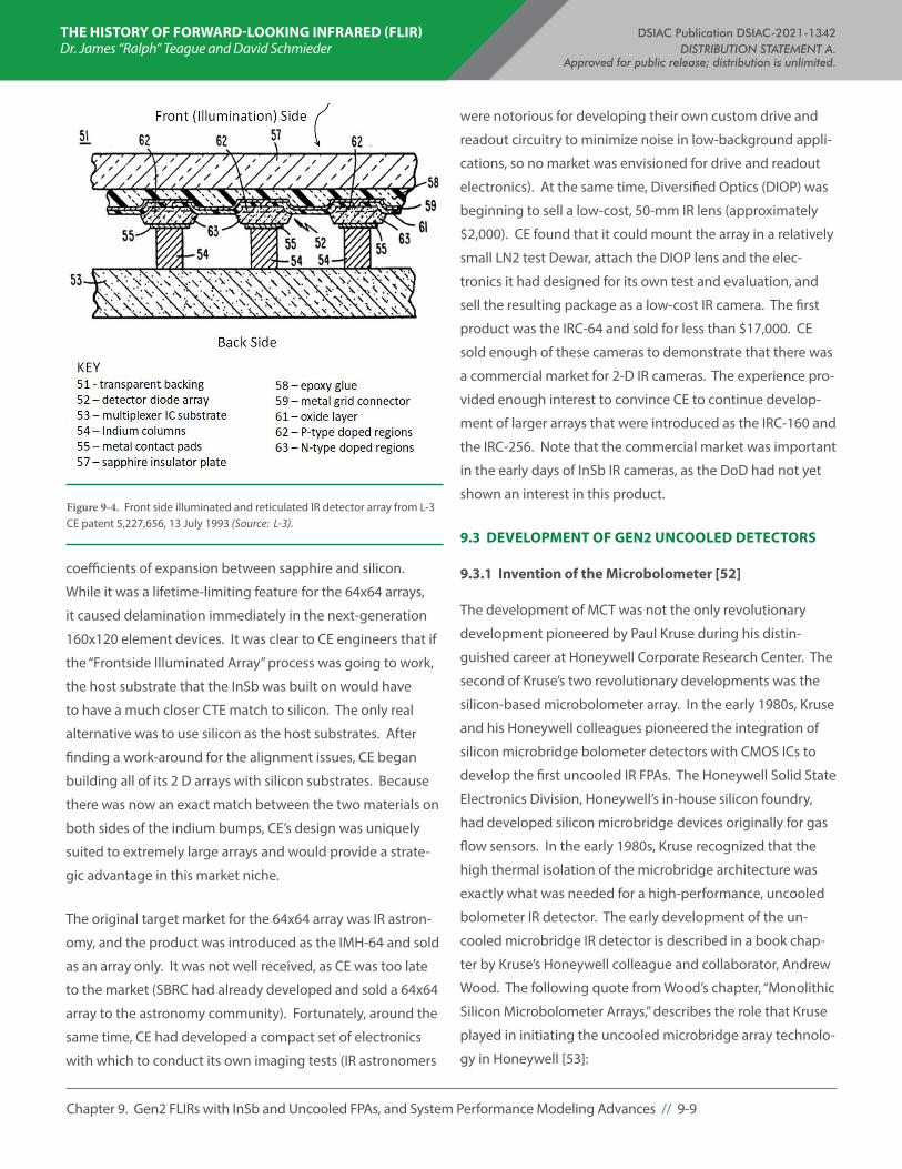
THE HISTORY OF FORWARD-LOOKING INFRARED (FLIR) DSIAC Publication DSIAC-2021-1342 Dr. James “Ralph” Teague and David Schmieder DISTRIBUTION STATEMENT A. Approved for public release; distribution is unlimited.
Chapter 9. Gen2 FLIRs with InSb and Uncooled FPAs, and System Performance Modeling Advances // 9-9
coefficients of expansion between sapphire and silicon.
While it was a lifetime-limiting feature for the 64x64 arrays,
it caused delamination immediately in the next-generation
160x120 element devices. It was clear to CE engineers that if
the “Frontside Illuminated Array” process was going to work,
the host substrate that the InSb was built on would have
to have a much closer CTE match to silicon. The only real
alternative was to use silicon as the host substrates. After
finding a work-around for the alignment issues, CE began
building all of its 2 D arrays with silicon substrates. Because
there was now an exact match between the two materials on
both sides of the indium bumps, CE’s design was uniquely
suited to extremely large arrays and would provide a strate-
gic advantage in this market niche.
The original target market for the 64x64 array was IR astron-
omy, and the product was introduced as the IMH-64 and sold
as an array only. It was not well received, as CE was too late
to the market (SBRC had already developed and sold a 64x64
array to the astronomy community). Fortunately, around the
same time, CE had developed a compact set of electronics
with which to conduct its own imaging tests (IR astronomers
were notorious for developing their own custom drive and
readout circuitry to minimize noise in low-background appli-
cations, so no market was envisioned for drive and readout
electronics). At the same time, Diversified Optics (DIOP) was
beginning to sell a low-cost, 50-mm IR lens (approximately
$2,000). CE found that it could mount the array in a relatively
small LN2 test Dewar, attach the DIOP lens and the elec-
tronics it had designed for its own test and evaluation, and
sell the resulting package as a low-cost IR camera. The first
product was the IRC-64 and sold for less than $17,000. CE
sold enough of these cameras to demonstrate that there was
a commercial market for 2-D IR cameras. The experience pro-
vided enough interest to convince CE to continue develop-
ment of larger arrays that were introduced as the IRC-160 and
the IRC-256. Note that the commercial market was important
in the early days of InSb IR cameras, as the DoD had not yet
shown an interest in this product.
9.3 DEVELOPMENT OF GEN2 UNCOOLED DETECTORS
9.3.1 Invention of the Microbolometer [52]
The development of MCT was not the only revolutionary
development pioneered by Paul Kruse during his distin-
guished career at Honeywell Corporate Research Center. The
second of Kruse’s two revolutionary developments was the
silicon-based microbolometer array. In the early 1980s, Kruse
and his Honeywell colleagues pioneered the integration of
silicon microbridge bolometer detectors with CMOS ICs to
develop the first uncooled IR FPAs. The Honeywell Solid State
Electronics Division, Honeywell’s in-house silicon foundry,
had developed silicon microbridge devices originally for gas
flow sensors. In the early 1980s, Kruse recognized that the
high thermal isolation of the microbridge architecture was
exactly what was needed for a high-performance, uncooled
bolometer IR detector. The early development of the un-
cooled microbridge IR detector is described in a book chap-
ter by Kruse’s Honeywell colleague and collaborator, Andrew
Wood. The following quote from Wood’s chapter, “Monolithic
Silicon Microbolometer Arrays,” describes the role that Kruse
played in initiating the uncooled microbridge array technolo-
gy in Honeywell [53]:
Figure 9-4. Front side illuminated and reticulated IR detector array from L-3 CE patent 5,227,656, 13 July 1993 (Source: L-3).
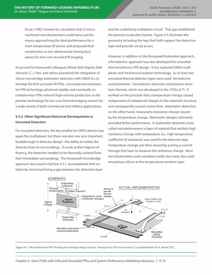
THE HISTORY OF FORWARD-LOOKING INFRARED (FLIR) DSIAC Publication DSIAC-2021-1342 Dr. James “Ralph” Teague and David Schmieder DISTRIBUTION STATEMENT A. Approved for public release; distribution is unlimited.
Chapter 9. Gen2 FLIRs with InSb and Uncooled FPAs, and System Performance Modeling Advances // 9-10
Kruse (1982) showed by calculation that Si micro-
machined microbolometers could have a perfor-
mance approaching the ideal performance for a
room temperature IR sensor, and proposed their
construction as two-dimensional staring focal
planes for low-cost uncooled IR imaging.
Kruse and his Honeywell colleagues Wood, Bob Higashi, Bob
Johnson, C. J. Han, and others pioneered the integration of
silicon microbridge bolometer detectors with CMOS ICs to
develop the first uncooled IR FPAs. Uncooled microbolome-
ter FPA technology advanced rapidly, and eventually mi-
crobolometer FPAs entered high-volume production as the
premier technology for low-cost thermal imaging sensors for
a wide variety of both commercial and military applications.
9.3.2 Other Significant Historical Developments in
Uncooled Detectors
For uncooled detectors, the key enabler for GEN2 devices was
again the multiplexer, but there was also one very important
breakthrough in detector design: the ability to isolate the
detector from its surroundings. To work at their highest ef-
ficiency, the detectors needed to be thermally isolated from
their immediate surroundings. The Honeywell microbridge
approach discussed in Section 9.3.1, accomplished that iso-
lation by micromachining a gap between the detection layer
and the underlying multiplexer circuit. That gap established
the desired conduction barrier. Figure 9-5 illustrates the
geometry including the legs that both support the detection
layer and provide circuit access.
However, in addition to the Honeywell bolometer approach,
a ferroelectric approach was also developed for uncooled
thermal detector FPA design. It too exploited GEN2 multi-
plexer and mechanical isolation technology. So at least two
uncooled thermal detector types were used: ferroelectric
and bolometric. Ferroelectric detection used barium stron-
tium titanate, which was developed in the 1970s at TI. It
worked on the principle that a temperature change caused
realignment of unbalanced charges in the material’s structure
and subsequently caused current flow. Bolometric detection,
on the other hand, measured a resistance change caused
by the temperature change. Bolometric designs ultimately
provided better performance. In bolometer detectors (now
called microbolometers) a layer of material that exhibits high
resistance change with temperature (i.e., high temperature
coefficient of resistance) was used for the detector layer.
Temperature change was then sensed by pulsing a current
through that layer to measure the resistance change. Most
microbolometers used vanadium oxide, but many also used
amorphous silicon as the temperature-sensitive layer.
Figure 9-5. Microbolometer FPA showing microbridge design (Source: Georgia Tech ITA course notes [1] as adapted from R. A. Wood [53]).
THE HISTORY OF FORWARD-LOOKING INFRARED (FLIR) DSIAC Publication DSIAC-2021-1342 Dr. James “Ralph” Teague and David Schmieder DISTRIBUTION STATEMENT A. Approved for public release; distribution is unlimited.
Chapter 9. Gen2 FLIRs with InSb and Uncooled FPAs, and System Performance Modeling Advances // 9-11
Uncooled detector FPAs did not perform as well as cooled
FPAs, but they offered lower cost in smaller, lighter packages
and still provided performance comparable, or better than,
GEN1 FLIRs with cooled detectors. Those features opened
up a wide range of applications that would not have been
as viable had cooled devices been the only option. Such
applications ranged from man-portable rifle sights to night
driver aids to missile seekers. Automobile manufacturers
found them compelling enough that General Motors, circa
2000, offered them as a $5,000 extra cost option on Cadillacs.
Others followed, and commercial applications soon opened
up ranging from security cameras to night vision devices for
law enforcement.
9.4 ADVANCEMENTS IN FLIR MODELING AND ANALYSIS [1]
9.4.1 FLIR Modeling Developments Overview
The development of analytical tools to predict the perfor-
mance of FLIRs played a significant role in both optimizing
FLIR system parameters (focal length, aperture size, video
bandwidth, display design, etc.) and focusing attention on
key component technologies where improvement would
provide the most system performance. This section address-
es recent advances such as in optimizing GEN2 designs by
understanding the important effects of fixed-pattern noise
(FPN, also called spatial noise, as previously discussed in
Section 9.2.3) display size/viewing distance, observer filtering
of FPN, and the effects of observer eye noise. Without this
understanding , as captured in FLIR performance prediction
models, GEN2 FLIRs could not have reached their full poten-
tial. Finally, new FLIR designs and optimal utilization of past
FLIR generations still in-service have benefitted from ongo-
ing studies of the significant impact that background clutter
plays in observer target acquisition. Those studies, with their
findings and conclusions, are also addressed in this section.
9.4.2 System and Observer Noise Modeling for GEN2
FLIRs
As mentioned in previous chapters, Fred Rosell, Bob Sendall,
and others pioneered the understanding of human visual
system psychophysical factors involved in viewing fast fram-
ing video information display. Their work was captured in an
NVL computer modeling code by James Ratches [41] and his
colleagues at NVL [25]. It was used extensively for optimizing
GEN1 FLIRs including the writing of design manuals [46].
However, early models were not adequate for predicting
the performance of GEN2 FLIRs. One problem was that
GEN1 models were largely optimized for one-dimensional,
horizontal-scanning, linear arrays, and not for 2-D, staring,
FPA-equipped imagers. Moreover, the GEN2 FLIRs were so
much more sensitive that their temporal noise levels were
now comparable to those found in the human eye. Therefore,
human eye noise levels had to be understood and included
in the noise models. In addition, temporal noise was at first
smaller than spatial noise until techniques were developed
to suppress the latter and until criteria were developed to
determine how much suppression was required.
Spatial noise was noticeable in scanned GEN1 FLIRs as well,
but it was only in the vertical direction since each horizontal
scan line was generated by a different detector. Even then
detector/amplifier/LED response differences were largely
compensated for by factory-set, field-maintainable, potenti-
ometers that reduced channel imbalances. But residual im-
balances still existed in the vertically arrayed raster lines due
to drift over time, temperature changes, etc. More important-
ly, the pixel dwell time of the scanning detectors was much
shorter than in GEN2 staring detectors so the former had less
exposure to the background flux and thus correspondingly
lower FPN. While the GEN1 vertical FPN was smaller, it was
also less noticeable due to both the much higher apparent
temporal noise of the GEN1 FLIR and the scan line raster
structure itself. Finally, models only addressed GEN1 perfor-
mance in the horizontal scanning direction so vertical FPN
was not even accounted for.
Surprisingly, when early GEN2 FLIR performance was first
measured in the field, it was found to be substantially less
than what was predicted by existing models. The main
reason was the poor understanding of the effect of FPN
THE HISTORY OF FORWARD-LOOKING INFRARED (FLIR) DSIAC Publication DSIAC-2021-1342 Dr. James “Ralph” Teague and David Schmieder DISTRIBUTION STATEMENT A. Approved for public release; distribution is unlimited.
Chapter 9. Gen2 FLIRs with InSb and Uncooled FPAs, and System Performance Modeling Advances // 9-12
on overall observer noise perception [54] and subsequent
underestimation of its impact. That impact included the
debilitating effect of amplifier boost or aperture correction,
i.e., the process of preferentially increasing amplifier gain at
higher frequencies to mitigate resolution roll-off due to such
effects as optical diffraction and detector size. GEN1 FLIRs
used high levels of boost but only applied it in the horizon-
tal scan direction since that was all they could effectively
do with horizontally scanned discrete detectors and analog
electronics. So, there was no amplification of the FPN. Now,
since GEN2 FPAs had nonuniform detector response in the
horizontal direction as well, high-frequency gain also prefer-
entially increased the FPN which, in turn, imposed a limit on
how much gain was useful.
Human factors research conducted at the Army NVESD
(formerly NVL) by John D’Agostino and Curtis Webb [54]
provided the scientific basis for model improvements with
assistance from Richard Vollmerhausen [private communica-
tion, circa 2006], Barbara O’Kane, Mel Friedman, and others.
Ronald Driggers et al. [55] and many others at NVESD, ONR,
and U.S. Army Training and Doctrine Command [25] captured
and extended these later findings in greatly improved com-
puter codes that allowed GEN2 FLIR designs to be further
optimized and thus come closer to realizing their potential.
9.4.3 Background Clutter Modeling
A key gap in FLIR performance prediction analysis and mod-
eling was recognized in the early 1980s when the Air Force
initiated a program called the Tactical Decision Aid (TDA).
While the program started in that period, it initiated a long
series of research programs that were greatly expanded over
the ensuing decades and were still ongoing at the time of
this book writing. The goal of the TDA program was to pro-
vide mission planners with a prediction tool that would allow
them to prebrief pilots on critical aspects of their targeting
process. With the proliferation of airborne FLIR targeting
systems, it soon became apparent that pilots and/or their
weapons system operators (WSOs) needed help because
their survival depended on it. The targeting process often
required pilots to fly at high altitudes so they had a clear
line-of-sight to their targets, i.e., one not obscured by tree
lines and hills or other masking obstacles. But then enemy
radar and optical air defense systems could more easily spot
and shoot them down. It was critical that pilots be able to
quickly locate their targets to minimize their exposure to
enemy defenses. Hence, it was important to not only know
where to look, but to know what characteristics of the target
to look for. For instance, was it positive or negative contrast?
Would it have a strong, positive contrast signature, such as
an armored air defense unit that had been exposed to solar
heating all day? In the latter case, its heavy armor would
retain heat long after a lighter foliage background cooled
off at night. Or would it have a strong negative contrast,
after the sun came up in the morning? In this case, it would
take much longer for heavy armor to heat up than would
the much lighter background foliage. Such information was
even more critical for the mission planner because it would
allow them, with the benefit of TDA software, to predict the
range at which the pilot could detect the target so they could
“popup” at that range and thus minimize the time they would
spend exposed to enemy fire. Many phenomena had to be
included in the TDA software such as weather predictions
and their effect on signature generation and propagation. Of
course, FLIR performance characteristics would be critical.
The Avionics Laboratory at Wright-Patterson AFB asked
co-author David Schmieder if he and his employer, Georgia
Tech Research Institute, could provide FLIR modeling help
based on his industry experience modeling and designing
FLIRs while employed at Martin Marietta, now Lockheed Mar-
tin. Schmieder accepted the assignment but realized that
then-current performance prediction models were missing
critical FLIR performance criteria necessary for the TDA. That
missing criteria included the resolution required by a FLIR
to allow the operator to perform target detection in varying
degrees of background clutter. The venerable Johnson bar
target equivalency resolution criteria for target detection
did not control for background clutter, nor was there even a
metric that could characterize and quantify clutter.
THE HISTORY OF FORWARD-LOOKING INFRARED (FLIR) DSIAC Publication DSIAC-2021-1342 Dr. James “Ralph” Teague and David Schmieder DISTRIBUTION STATEMENT A. Approved for public release; distribution is unlimited.
Chapter 9. Gen2 FLIRs with InSb and Uncooled FPAs, and System Performance Modeling Advances // 9-13
The Air Force Avionics Lab accepted a proposal from Schmie-
der and his colleagues to perform a human factors study
using Georgia Tech students after target detection training
to repeat Johnson’s bar target equivalency measurements
for target detection. The goal was to measure detection
probability as a function of resolution for targets embedded
in varying, but controlled, amounts of background clutter.
To conduct the study, they had to first determine a clutter
metric. Kowalczyk and Rotman described the outcome in
Chapter 28 of Biberman’s 2000 book, Electro-Optical Imaging:
System Performance and Modeling [25] this way:
In the early 1980s a method based on the “av-
erage” scene radiance (or equivalent) standard
deviation was proposed by Schmieder and his
coworkers at Georgia Institute of Technology
[56]. This method partitioned the image into
square blocks (approximately twice the size of
the target), calculated the variance of the pixel
intensities within each block, then root mean
square averaged the result over all the blocks.
The authors called this the “rms clutter variance.”
Since that time others have referred to this as the
“Schmieder Statistical Variance” (or SV).
…A combined measure called the signal to clutter
ratio (SCR) was defined as the maximum (or, if
negative, absolute) difference between the target
and background mean radiance divided by the
rms clutter radiance.
…The approach … was a major advance since for
the first time, it was possible to calculate a target
transfer probability Function (TTPF) curve for a
specific level of clutter in an image.
While the study results were immediately incorporated into
Air Force TDA software, the study authors regarded their
definition of both signal and clutter as merely an embryonic
start on a long journey to refine the definition of both clutter
and signal as progress in image understanding science pro-
gressed. Moreover, the initial study only applied to natural
backgrounds. A later study by Cathcart, Doll, and Schmieder
extended the results to urban backgrounds [57]. Many stud-
ies subsequently followed as other researchers took up the
quest. The result was ongoing continuous evolution in crite-
ria for the resolution required for FLIRs when used for target
detection as described in a 2015 Sandia report [58]. The Navy
and Army soon also adopted TDAs as mission planning tools
for their air crew mission planning needs.
9.5 SUMMARY
This chapter described the evolution and development of
GEN2 FLIR technology up to approximately the mid-2000s to
2010. It focused on InSb as the material that resulted in the
emergence of affordable 2-D staring arrays and their role in
the development of large FPA formats. While MCT was the
material of choice for ground-to-ground combat for various
reasons including its better penetration through battlefield
smoke and dust and its greater sensitivity in cold climates,
InSb was better suited for airborne applications. This suitabil-
ity for airborne applications was due to its shorter wave-
length operating band which allowed for smaller apertures,
with attendant reduction in SWaP-C, without sacrificing
range. Moreover, aircraft could fly above the battlefield fray
and did not need the better smoke and dust penetration as
much as ground units. In addition, the emergence of FLIRs
with uncooled FPAs opened a whole new realm of applica-
tions that were now practical because of their much lower
cost and size. By the mid-2000s to 2010, FLIR technology had
evolved to where it provided a robust solution to the histor-
ical demands of the battlefield, but this period was dynamic
and was by no means nearing its full potential.
The optimization of GEN2 FLIRs demanded better modeling
and analysis capabilities for their promise to be realized.
Fixed pattern noise severely limited their performance until it
was recognized and suppressed. Greater GEN2 sensitivity re-
sulted in so much lower display noise that it rivaled the noise

THE HISTORY OF FORWARD-LOOKING INFRARED (FLIR) DSIAC Publication DSIAC-2021-1342 Dr. James “Ralph” Teague and David Schmieder DISTRIBUTION STATEMENT A. Approved for public release; distribution is unlimited.
Chapter 9. Gen2 FLIRs with InSb and Uncooled FPAs, and System Performance Modeling Advances // 9-14
inherent in observers. Thus, models had to now take observ-
er eye noise into account to correctly predict “system-observ-
er” performance.
Finally, the practical military need to plan missions for opti-
mum air crew survivability led to factoring in the complexi-
ties of background clutter into the design of FLIR targeting
systems. The variety and complexity of backgrounds led to
new definitions of both clutter and target signature. These
background considerations brought new insights into the
psychophysics of the human vision system that is ongoing
and likely to continue yielding new insights into FLIR design
optimization.
THE HISTORY OF FORWARD-LOOKING INFRARED (FLIR) DSIAC Publication DSIAC-2021-1342 Dr. James “Ralph” Teague and David Schmieder DISTRIBUTION STATEMENT A. Approved for public release; distribution is unlimited.
Chapter 10. Summary, Current Trends, and Lessons for the Future // 10-1
CHAPTER 10. SUMMARY, CURRENT TRENDS, AND LESSONS FOR THE FUTURE10.1 INTRODUCTION 20
IR technology has undergone a remarkable transformation
over the last 50-plus years. As of 2016, it has played a critical
role in U.S. defense capability by providing the day and night
vision that gives U.S. forces a major advantage. Of course, the
real value of any history is the lessons it holds for the path
forward. To speculate on that path, this chapter first provides
a summary of FLIR military history and then discusses current
trends and apparent direction. The goal is to discuss FLIR
technology as of the date of this book and to set a baseline
for speculating on the path forward. Final conclusions offer
thoughts on the path forward and on the lessons for guiding
military FLIR technology on that path.
10.2 SUMMARY
The history of military FLIRs discussed in this book has
focused on the key enabling technologies that contributed
to their development. However, many more supporting
technologies were required for FLIR development than were
discussed in this book. Examples are advances in optical
lens and coating materials, digital microelectronic integrat-
ed circuits, cryocoolers, and Dewars. Also important were
phenomenology studies such as atmospheric absorption and
scattering as well as scene and target signature studies that
helped analysts predict FLIR performance. Those technol-
ogies and studies, with their impact on FLIR development,
should not be minimized but their history is either left to
others to write or have already been written and published in
various books and journals.
20 The discussion of current trends and future projections includes excerpts from Teague and Schmieder’s paper in the fall 2015 issue of the DSIAC Journal [59].
With the above caveats in mind and for the purpose of a
broad overview summary, the following chronology lists sig-
nificant events leading to or directly addressing the history of
U.S. FLIR technology development up to the early 2000s:
• 1800: Astronomer Sir William Herschel discovered the IR region of the electromagnetic spectrum.
• Mid-1930s: PbS photoconductive detectors were invent-ed and used in early search systems.
• 1950–1960: Single-element detectors produced line scan images of scenes that enabled finding and tracking enemy dismount forces.
• 1954: Otto Schade introduced the concept of Modula-tion Transfer Function (MTF) as a metric for quantifying the resolution of image-forming systems.
• 1958: John Johnson introduced the concept of “bar tar-get equivalency” as a metric for quantifying the resolu-tion needed for varying levels of target acquisition.
• Late 1950s: William Lawson discovered MCT IR detector properties.
• Early 1960s: Paul Kruse and his colleagues at Honeywell discovered methods to fabricate MCT detectors.
• 1968: Robert Sendall introduced the aggregate FLIR metric Minimum Resolvable Temperature (MRT) that made it possible to optimize FLIR performance.
• Early 1970s: Common module building blocks for FLIRs were developed, thus enabling affordable, mass-pro-duced, GEN1 FLIRs that were made from discrete-ele-ment, photoconductive MCT detector technology.
• 1970s–1980s: Analog multiplexers were developed that led to the fabrication of large-detector-count GEN2 ar-rays; MCT and InSb detector technology efforts focused on photovoltaic design and producibility.
• Mid-1980s: Paul Kruse and his colleagues at Honeywell invented microbolometer FPA technology and devel-oped uncooled IR FPAs.

THE HISTORY OF FORWARD-LOOKING INFRARED (FLIR) DSIAC Publication DSIAC-2021-1342 Dr. James “Ralph” Teague and David Schmieder DISTRIBUTION STATEMENT A. Approved for public release; distribution is unlimited.
Chapter 10. Summary, Current Trends, and Lessons for the Future // 10-2
• 1980s–1990s: Significant progress was made on large, 2-D InSb FPAs and uncooled device technologies. MCT technology efforts focused on GEN2 scanning devices.
• 1990s–2000s: Initial technology development began on MCT dual-band devices; MCT, InSb, and uncooled 2-D staring devices were used widely in applications includ-ing targeting and surveillance systems, missile seekers, driver aids, and weapon sights.
Substantial government funds were expended to insert these
now-proven IR devices into military payloads and missile
seekers and later into commercial products. As a result of
the success of military research and development programs,
new applications were identified, and products were moved
into production. Thermal imaging technology provided the
ability to see and target opposing forces at night and across
smoke- and dust-covered battlegrounds. These capabilities
backed the Army’s claim that “we own the night.”
10.3 CURRENT TRENDS AND FUTURE PROJECTIONS
Urban Warfare Requirements. As a key military technology,
FLIR development has always been driven by the evolution of
the threat. A major concern has been threats that come from
adversaries that employ unconventional tactics (i.e., terrorists
and insurgents), but that does not mean adversaries that
employ conventional tactics can be ignored. Traditionally,
the U.S. military has chosen to avoid close combat in cities
in preference to using its superiority in long range standoff
weapons to defeat conventional forces. Yet, evolving world
demographics coupled with political turmoil have drawn
conflict into urban areas. That fact is especially true in those
parts of the world that are becoming increasingly unstable
due to the combination of terrorism and hordes of refugees
attempting to escape violence and avoid starvation. These
urban areas provide a hiding place for radical extremists
where it is hard to deploy conventional weapons and tactics.
This situation has led to warfare that is increasingly fought
in urban environments. New kinds of high-performance IR
imaging systems already play a critical role in this warfare,
and the more advanced systems in development will likely
play an even larger role.
Success in urban warfare largely depends upon the ability to
accomplish the following (adapted from Carson [60]):
• Find and track enemy dismounted forces, even when their appearance is brief or mixed with the civilian pop-ulation.
• Locate their centers of strength (e.g., leadership, weap-ons caches, fortified positions, communication nodes, etc.), even when camouflaged or hidden in buildings.
• Attack both light and heavy targets with precision, with only seconds of latency and little risk to civilian popula-tions and infrastructure.
• Protect U.S. forces from individual and crew-served weapons, mines, and booby traps.
• Employ robots in the form of drones such as unmanned air vehicles and unmanned ground vehicles as well as unattended sensors.
• Protect our own forces and homeland infrastructure from these same drones, which in miniature, can fly in undetected while carrying miniature IR sensors that allow for precise day/night delivery of explosives.
Persistent Surveillance Systems. To meet these require-
ments imaging systems must provide persistent surveil-
lance from platforms located almost directly overhead and
from small, stationary, and maneuverable platforms on the
ground. Also needed are imaging systems that perform
targeting and fire control through haze, smoke, and dust.
Overhead systems must have the resolution to recognize dif-
ferences between civilian and military dismounts, and some
of them must perform change detection based on shape and
spectral features. Others must quickly detect and locate ene-
my weapons by their gun flash and missile-launch signatures.
Near-ground systems must have the resolution and sensi-
tivity to identify individuals, at relatively short ranges, from
their facial and clothing features and from what they are
carrying. They must also be able to do it through windows
and under all weather and lighting conditions. Some must
be able to see through obscurations, such as foliage and
camouflage netting. In most cases, collected imagery will be

THE HISTORY OF FORWARD-LOOKING INFRARED (FLIR) DSIAC Publication DSIAC-2021-1342 Dr. James “Ralph” Teague and David Schmieder DISTRIBUTION STATEMENT A. Approved for public release; distribution is unlimited.
Chapter 10. Summary, Current Trends, and Lessons for the Future // 10-3
transmitted to humans who are under pressure to examine it
and make quick, accurate decisions. As such, it is important
that imagery be highly intuitive and easily interpretable. This
persistent, up-close, and personal sensing strategy requires
many and varied platform types. Cost is an important factor
due to ongoing budget constraints. Not only the sensors, but
the platforms that carry them, must be affordable; but some
must also be man portable. Accordingly, many sensors must
be small and light.
Solutions to some of the surveillance requirements are being
addressed with current persistent surveillance systems
such as ARGUS-IS and ARGUS-IR (Figure 10-1). ARGUS-IS
has an enormous array of 368 optically butted FPAs using
four co-boresighted cameras. They combine for a total of
1.8 gigapixels that can provide separate images of 640x480
pixels to as many as 65 operators. The operators can then
independently track separate ground objects or persons of
interest within the ground footprint of the combined sensors
with a ground resolution of approximately 4 in. at a 15-kilo-
foot (kft) platform altitude. ARGUS-IS operates in the visible/
NIR band and requires daylight, but the DoD is developing
the more advanced ARGUS-IR to field comparable capability
at night.
Microbolometers. Other IR surveillance technologies
involve unattended sensors that can be covertly deployed in
either urban or rugged country terrain. Figure 10-2 shows an
example of how tiny uncooled LWIR microbolometers can be.
When triggered in the field, for instance, by a change detec-
tion software, they can snap a picture of passing insurgents
and feed that to the battlefield network for targeting. They
have low SWaP-C, are expendable, and can run for a long
time on batteries and solar power.
While the emergence of small surveillance drones has driven
the need for lower-weight and lower volume payloads, often
performance cannot be sacrificed, and microbolometers can-
not always meet these payload requirements. For these re-
quirements, there is on an ongoing drive for small-pitch FPAs
that operate at higher temperatures, often above 150 K. Overall
Figure 10-1. ARGUS-IS has 368 5-megapixel FPAs that provide 1.8 gigapixels on the ground with a resolution of 4 in. at 15 kft in the visible/near-IR band. One planned MWIR version (ARGUS-IR) would provide over 100 cooled FPAs each with 18 megapixels [61−63].
Figure 10-2. The Lepton microbolometer is an example of how small IR imaging sensors can be made. They can be used for covert, unattended op-eration in either remote or urban locations and connected to the battlefield network (Source: FLIR Inc.).

THE HISTORY OF FORWARD-LOOKING INFRARED (FLIR) DSIAC Publication DSIAC-2021-1342 Dr. James “Ralph” Teague and David Schmieder DISTRIBUTION STATEMENT A. Approved for public release; distribution is unlimited.
Chapter 10. Summary, Current Trends, and Lessons for the Future // 10-4
sensor size, for equal performance, scales with detector pitch
as long as the aperture size is maintained. Smaller pixels
allow for a reduction in the Dewar and cooler size and weight
and for reduction of the optical focal length. Accordingly,
package size and, to a large degree, package weight can be
reduced in proportion to detector pitch. The current trend
appears to be moving to 10–8-µm pitch for MWIR sensors,
but some LWIR FPAs are being made with the pitch as small
as 5 µm.
Emerging systems are being designed to counter the prolif-
eration of IR imagers in the hands of the insurgents as well.
Readily available commercial microbolometers are poten-
tially a major threat. Although these imagers typically have
lower resolution and sensitivity than what advanced technol-
ogy can provide, adversaries can effectively use these cheap,
low-resolution sensors and still fire at U.S. forces at long
ranges. To counter this threat, the Army’s desire for increased
standoff range resulted in development of a third generation
(GEN3) of staring sensors with both MWIR and LWIR capa-
bility. The shorter MWIR wavelength offers nearly twice the
range of the LWIR band in good weather, but the LWIR band
excels in battlefield smoke and dust and provides greater
range in cold climates.
GEN3 Technology. Currently, GEN3 technology is expensive.
The high cost is associated with both low detector yield and
complex optics. Detector cost is being addressed on two
fronts: alternate substrates and new detector materials. A
GEN3 detector is made by placing MWIR detector material
behind LWIR material so the two bands occupy the same
space in the focal plane. Currently, only two materials offer
this potential: MCT and superlattices. MCT is most easily
made on CdZnTe substrates because the lattices match well,
thus providing higher yield. However, lower-cost GaAs and
Si substrates are being explored with considerable success.
The other front exploits the potential for a radically different
material type called a superlattice. Superlattices exploit
nanotechnology to engineer materials from the III-V columns
of the periodic table to make alloys such as indium arsenide
antimonide (InAsSb) and indium arsenide (InAs). In principle,
they have many favorable characteristics such as strength,
stability, and low cost. However, they have wide band gaps.
To detect low-energy MWIR and LWIR photons, they have
to be fabricated in thin, alternating layers to form quantum
wells. Superlattices have the additional benefit of being
compatible with another breakthrough in detector design
called negative-barrier-negative junctions. The latter have an
advantage over traditional positive-negative junctions (such
as are commonly used in commercial solar cells) in that they
can better suppress the dark current that arises from latent
heat in the material. This characteristic, in turn, offers the
potential for higher-temperature operation. Current success
is so far largely in the MWIR region, but success is expected
in the LWIR region as well. It remains to be seen if it will be a
better solution than MCT.
The dual-band GEN3 approach is actually a subset of multi-
spectral and hyperspectral imaging. The latter offers ad-
ditional modalities and is often best exploited with sensor
fusion techniques. But it faces challenges and is still in
development. Multispectral images must be displayed or
processed simultaneously in each band to extract target
information. In addition, for operator viewing, they must be
combined into a single, composite image using a color vision
fusion approach. The best way to accomplish that fusion and
display it to an operator is still being investigated. However,
results have shown impressive reductions in false-alarm rate
and probability of missed detections when, for instance,
searching for targets hidden in deep tree canopies and/or
under camouflaged nets.
Passive/Active Fused Sensors. Airborne and Naval plat-
forms have taken an entirely different approach to gaining
extended-range target identification. Their approach can, in
principle, triple the range of existing targeting FLIRs. They
are adopting passive/active hybrid systems consisting of pas-
sive IR imaging for target detection in combination with ac-
tive lidar (light detection and ranging, analogous to radar as
“radio detection and ranging”) for high-resolution identifica-
tion. Figure 10-3 shows an example of this imagery provided
by BAE. The principle is that lidars can image with much
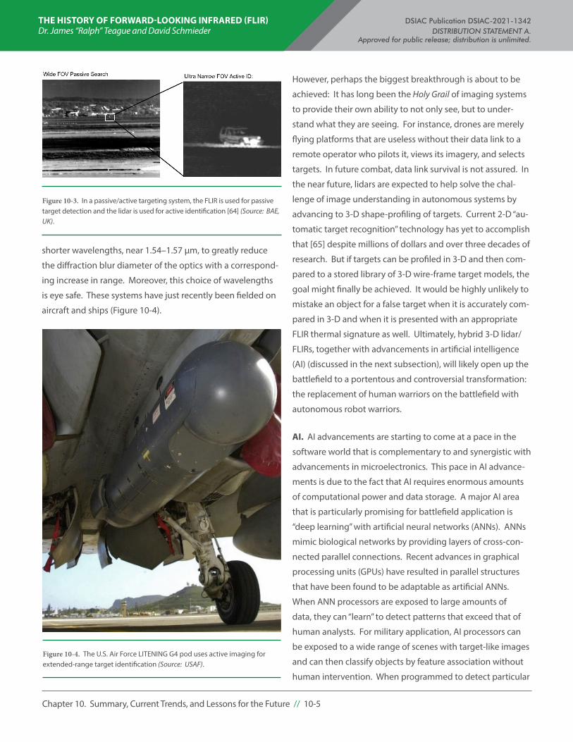
THE HISTORY OF FORWARD-LOOKING INFRARED (FLIR) DSIAC Publication DSIAC-2021-1342 Dr. James “Ralph” Teague and David Schmieder DISTRIBUTION STATEMENT A. Approved for public release; distribution is unlimited.
Chapter 10. Summary, Current Trends, and Lessons for the Future // 10-5
shorter wavelengths, near 1.54–1.57 µm, to greatly reduce
the diffraction blur diameter of the optics with a correspond-
ing increase in range. Moreover, this choice of wavelengths
is eye safe. These systems have just recently been fielded on
aircraft and ships (Figure 10-4).
However, perhaps the biggest breakthrough is about to be
achieved: It has long been the Holy Grail of imaging systems
to provide their own ability to not only see, but to under-
stand what they are seeing. For instance, drones are merely
flying platforms that are useless without their data link to a
remote operator who pilots it, views its imagery, and selects
targets. In future combat, data link survival is not assured. In
the near future, lidars are expected to help solve the chal-
lenge of image understanding in autonomous systems by
advancing to 3-D shape-profiling of targets. Current 2-D “au-
tomatic target recognition” technology has yet to accomplish
that [65] despite millions of dollars and over three decades of
research. But if targets can be profiled in 3-D and then com-
pared to a stored library of 3-D wire-frame target models, the
goal might finally be achieved. It would be highly unlikely to
mistake an object for a false target when it is accurately com-
pared in 3-D and when it is presented with an appropriate
FLIR thermal signature as well. Ultimately, hybrid 3-D lidar/
FLIRs, together with advancements in artificial intelligence
(AI) (discussed in the next subsection), will likely open up the
battlefield to a portentous and controversial transformation:
the replacement of human warriors on the battlefield with
autonomous robot warriors.
AI. AI advancements are starting to come at a pace in the
software world that is complementary to and synergistic with
advancements in microelectronics. This pace in AI advance-
ments is due to the fact that AI requires enormous amounts
of computational power and data storage. A major AI area
that is particularly promising for battlefield application is
“deep learning” with artificial neural networks (ANNs). ANNs
mimic biological networks by providing layers of cross-con-
nected parallel connections. Recent advances in graphical
processing units (GPUs) have resulted in parallel structures
that have been found to be adaptable as artificial ANNs.
When ANN processors are exposed to large amounts of
data, they can “learn” to detect patterns that exceed that of
human analysts. For military application, AI processors can
be exposed to a wide range of scenes with target-like images
and can then classify objects by feature association without
human intervention. When programmed to detect particular
Figure 10-3. In a passive/active targeting system, the FLIR is used for passive target detection and the lidar is used for active identification [64] (Source: BAE, UK).
Figure 10-4. The U.S. Air Force LITENING G4 pod uses active imaging for extended-range target identification (Source: USAF).
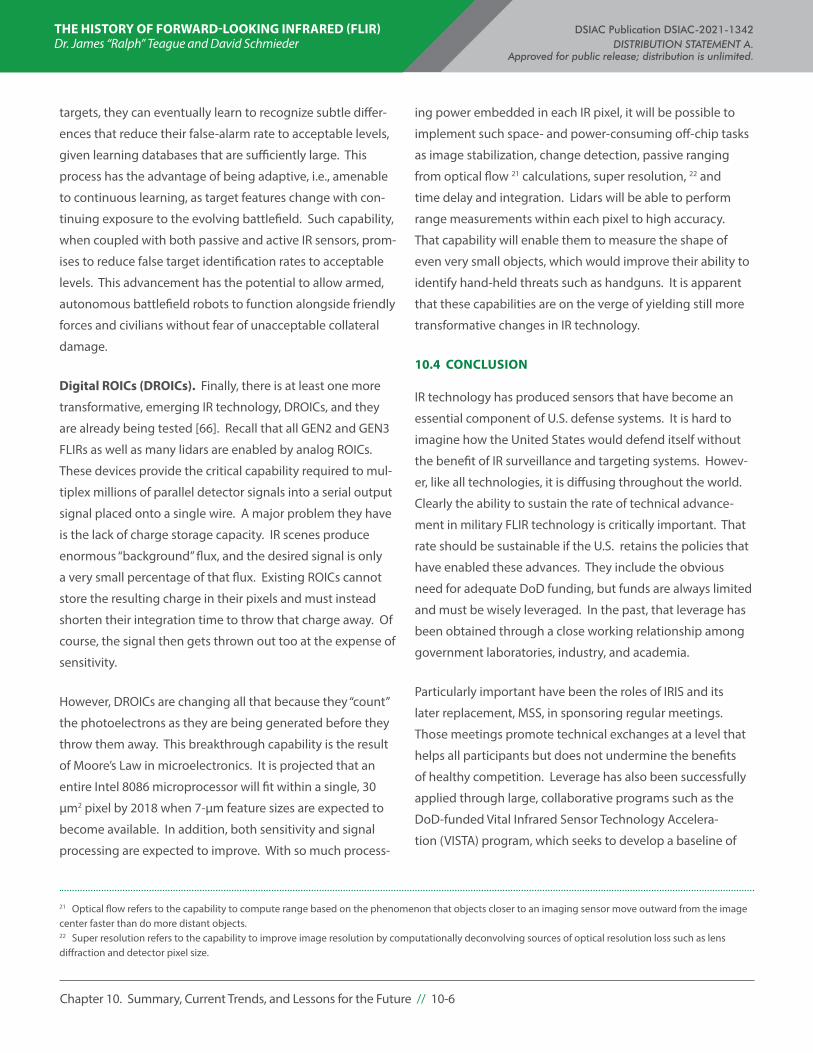
THE HISTORY OF FORWARD-LOOKING INFRARED (FLIR) DSIAC Publication DSIAC-2021-1342 Dr. James “Ralph” Teague and David Schmieder DISTRIBUTION STATEMENT A. Approved for public release; distribution is unlimited.
Chapter 10. Summary, Current Trends, and Lessons for the Future // 10-6
targets, they can eventually learn to recognize subtle differ-
ences that reduce their false-alarm rate to acceptable levels,
given learning databases that are sufficiently large. This
process has the advantage of being adaptive, i.e., amenable
to continuous learning, as target features change with con-
tinuing exposure to the evolving battlefield. Such capability,
when coupled with both passive and active IR sensors, prom-
ises to reduce false target identification rates to acceptable
levels. This advancement has the potential to allow armed,
autonomous battlefield robots to function alongside friendly
forces and civilians without fear of unacceptable collateral
damage.
Digital ROICs (DROICs). Finally, there is at least one more
transformative, emerging IR technology, DROICs, and they
are already being tested [66]. Recall that all GEN2 and GEN3
FLIRs as well as many lidars are enabled by analog ROICs.
These devices provide the critical capability required to mul-
tiplex millions of parallel detector signals into a serial output
signal placed onto a single wire. A major problem they have
is the lack of charge storage capacity. IR scenes produce
enormous “background” flux, and the desired signal is only
a very small percentage of that flux. Existing ROICs cannot
store the resulting charge in their pixels and must instead
shorten their integration time to throw that charge away. Of
course, the signal then gets thrown out too at the expense of
sensitivity.
However, DROICs are changing all that because they “count”
the photoelectrons as they are being generated before they
throw them away. This breakthrough capability is the result
of Moore’s Law in microelectronics. It is projected that an
entire Intel 8086 microprocessor will fit within a single, 30
µm2 pixel by 2018 when 7-µm feature sizes are expected to
become available. In addition, both sensitivity and signal
processing are expected to improve. With so much process-
21 Optical flow refers to the capability to compute range based on the phenomenon that objects closer to an imaging sensor move outward from the image center faster than do more distant objects.22 Super resolution refers to the capability to improve image resolution by computationally deconvolving sources of optical resolution loss such as lens diffraction and detector pixel size.
ing power embedded in each IR pixel, it will be possible to
implement such space- and power-consuming off-chip tasks
as image stabilization, change detection, passive ranging
from optical flow 21 calculations, super resolution, 22 and
time delay and integration. Lidars will be able to perform
range measurements within each pixel to high accuracy.
That capability will enable them to measure the shape of
even very small objects, which would improve their ability to
identify hand-held threats such as handguns. It is apparent
that these capabilities are on the verge of yielding still more
transformative changes in IR technology.
10.4 CONCLUSION
IR technology has produced sensors that have become an
essential component of U.S. defense systems. It is hard to
imagine how the United States would defend itself without
the benefit of IR surveillance and targeting systems. Howev-
er, like all technologies, it is diffusing throughout the world.
Clearly the ability to sustain the rate of technical advance-
ment in military FLIR technology is critically important. That
rate should be sustainable if the U.S. retains the policies that
have enabled these advances. They include the obvious
need for adequate DoD funding, but funds are always limited
and must be wisely leveraged. In the past, that leverage has
been obtained through a close working relationship among
government laboratories, industry, and academia.
Particularly important have been the roles of IRIS and its
later replacement, MSS, in sponsoring regular meetings.
Those meetings promote technical exchanges at a level that
helps all participants but does not undermine the benefits
of healthy competition. Leverage has also been successfully
applied through large, collaborative programs such as the
DoD-funded Vital Infrared Sensor Technology Accelera-
tion (VISTA) program, which seeks to develop a baseline of

THE HISTORY OF FORWARD-LOOKING INFRARED (FLIR) DSIAC Publication DSIAC-2021-1342 Dr. James “Ralph” Teague and David Schmieder DISTRIBUTION STATEMENT A. Approved for public release; distribution is unlimited.
Chapter 10. Summary, Current Trends, and Lessons for the Future // 10-7
shared technical knowledge and fabrication infrastructure.
Thus, each participating company does not have to make a
separate, redundant investment in those critical underpin-
ning capabilities. Yet those companies can add value by the
way they manage the products and innovate beyond that
framework.
So far, advances in IR technology have been driven by ad-
vances in materials, in microelectronics, and in understand-
ing human visual perception. However, also important, have
been the intangible benefits of the close working relation-
ships among government laboratories, industry, and aca-
demia. Microelectronics feature sizes have been shrinking
exponentially by Moore’s Law. But even if this pace slows,
advancement can be expected to be rapid going forward giv-
en the synergy between microelectronics and software such
as AI. Moreover, microelectronics has room to advance in
ways that do not necessarily depend on ever-smaller feature
sizes. Examples are structural improvements in chip design
such as those in GPUs and in 3-D chip configurations down
to the transistor level. While such advances are inexorable, it
can be argued that building upon the lessons of the past will
lower the cost, help sustain, and may even speed up the rap-
id pace of transformative changes in military FLIR technology
that brought it to where it is today.
THE HISTORY OF FORWARD-LOOKING INFRARED (FLIR) DSIAC Publication DSIAC-2021-1342 Dr. James “Ralph” Teague and David Schmieder DISTRIBUTION STATEMENT A. Approved for public release; distribution is unlimited.
References // R-1
REFERENCES1. Schmieder, D. E. “Infrared Technology and Applications.” Course
Notes, Georgia Institute of Technology, 2015.
2. Schmieder, D. E., and G. Walker. The Infrared & Electro-Optical Systems Handbook. Vol. 7, Chapter 2, 1993.
3. Rogalski, A. “Infrared Detectors: An Overview.” Infrared Physics & Technology, vol. 43, pp. 187–210, 2002.
4. Herschel, W. “Experiments on the Refrangibility of the Invisible Rays of the Sun.” Philos. Trans. Roy. Soc. London, vol. 90, pg. 284, 1800.
5. Wikipedia, “Thermographic Camera.” https://en.wikipedia.org/wiki/Thermographic_camera, accessed 16 June 2016.
6. Barr, E., and E. Scott. “Historical Survey of the Early Develop-ment of the Infrared Spectral Region.” American Journal of Physics, vol. 28, pp. 42–54, 1960.
7. Arnquist, W. N. “Survey of Early Infrared Developments.” Pro-ceedings of the IRE, September 1959.
8. Hudson, R. D. Infrared System Engineering. John Wiley & Sons, Inc., 1969.
9. Smith, W. “Effect of Light on Selenium During the Passage of an Electric Current.” Nature, vol. 7, pg. 303, 1873.
10. Bose, J. C. “Detector for Electrical Disturbances.” U.S. Patent No. 755,840 A, filed 30 September 1901, issued 29 March 1904.
11. Case, T. W. “Infrared Telegraphy and Telephony.” Journal of the Optical Society of America, vol. 6, pp. 39–406, 1922.
12. Rogalski, A. “History of Infrared Detectors.” Opto-Electronics Review, vol. 20, no. 3, 2012.
13. Sturdevant, R. W. “From the Pied Piper Infrared Reconnaissance Subsystem to the Missile Defense Alarm System: Space-Based Early Warning and Development, 1955–1970.” American Institute of Aeronautics and Astronautics (AIAA) Space 2010 Conference, Anaheim, CA, 2010.
14. Lovell, D. J. “Some Early Lead Salt Detector Developments.” Air Force Office of Scientific Research (AFOSR)-68-0264, University of Michigan, 1968.
15. Johnson, T. H. “Lead Salt Detectors and Arrays PbS and PbSe.” Proceedings of the International Society for Optical Engineering (SPIE), vol. 0443, 9 December 1983.
16. Lovell, D. J. “The Development of Lead Salt Detectors.” Ameri-can Journal of Physics, vol. 37, pg. 467, 1969.
17. Williams, R. “The Last Panther in Pomerania.” http://www.miss-ing-lynx.com/articles/dio/rwpanth/rwpanth_solutions.htm, accessed 14 July 2017.
18. Johnston, S. F. A History of Light and Colour Measurement: Sci-ence in the Shadows. IOP Publishing Ltd, 2001.
19. Sendall, R. “Documents Written for SENSIAC by Request.” Hughes Aircraft Company (HAC), Raytheon, 2014.
20. Jost, S. “Documents Written for SENSIAC by Request.” General Electric (GE), Sanders, Loral, Lockheed Martin Corporation (LMCO), BAE, 2013.
21. Taylor, K. “Documents Written for SENSIAC by Request.” Texas Instruments (TI), DRS Technologies, Inc., 2014.
22. Hudson, R. IR Systems Engineering. Wiley, 1969.
23. Communications-Electronics Research, Development, and Engineering Center (CERDEC). “History of Army Night Vision.” https://www.cerdec.army.mil/inside_cerdec/nvesd/history/, accessed 19 August 2015.
24. Wolfe, W. L. (editor). Handbook of Military IR Technology. Naval Research Laboratory (NRL), 1965.
25. Biberman, L. M. (editor). Electro-Optical Imaging: System Perfor-mance and Modeling. SPIE Press, ONTAR Corp., 2000.
26. Wolfe, W. L., and G. J. Zissis (editors). The IR Handbook. NRL, Environmental Research Institute of Michigan (ERIM), Infrared Information Analysis Center (IRIA), 1978.
27. Accetta, J. S., and D. L. Shumaker (editors). The IR & Electro-Opti-cal Systems Handbook. ERIM/SPIE, 1993.
28. Kruse, P. W., L. D. McGlauchlin, and R. B. McQuistan. Elements of IR Technology. Wiley, 1962.
29. Ponomarenko, V. P., and A. M. Filachev. Infrared Techniques and Electro-Optics in Russia: A History 1946–2006. SPIE Press, 2007.
30. Lawson, W. D., S. Nielson, E. H. Putley, and A. S. Young. “Prepara-tion and Properties of HgTe and Mixed Crystals of HgTe-CdTe.” J. Phys. Chem. Solids, vol. 9, pp. 325–329, 1959.
31. Kruse, P. W., M. D. Blue, J. H. Garfunkel, and W. D. Saur. “Long Wavelength Photoeffects in Mercury Cadmium Telluride.” IR Physics, vol. 2, pp. 53–60, 1962.
32. Elliott, T. “Recollections of MCT Work in the UK at Malvern and Southampton.” Proceedings of SPIE, vol. 7298, 2009.
33. Talley, R. “A History of Santa Barbara Research Center.” Santa Barbara Research Center (SBRC)/Raytheon Vision Systems, July 1995.
34. Hunt, G. R., J. W. Salisbury, and W. E. Alexander. “Thermal Enhancement Techniques: Application to Remote Sensing of Thermal Targets.” Res. Appl. Conf. Proceedings, Office of Aero-space Research, Washington, DC, pp. 113–120, March 1967.
35. Harris, D. E, and C. L. Woodbridge. National Electronics Confer-ence. Vol. 18, 1962.
36. TI. www.ti.com/corp/docs/company/history/timeline, accessed 21 April 2016.
37. Johnson, J. Image Intensifier Symposium. Fort Belvoir, VA, October 1958.
38. Schade, O. H. “A New System of Measuring and Specifying Image Definition.” Symposium on Optical Image Evaluation, NBS Circular, 1954.
39. Rosell, F. A. “Limiting Resolution of Low-Light-Level Imaging Sensors.” J. Opt. Soc. Am., vol. 59, no. 5, pp. 539–547.
THE HISTORY OF FORWARD-LOOKING INFRARED (FLIR) DSIAC Publication DSIAC-2021-1342 Dr. James “Ralph” Teague and David Schmieder DISTRIBUTION STATEMENT A. Approved for public release; distribution is unlimited.
References // R-2
40. Sendall, R. L., and F. A. Rosell. “E/O Sensor Performance Analysis and Synthesis (TV/IR Comparison Study).” Air Force Systems Command, 4950th Test Wing PMMA, Wright-Patterson Air Force Base (AFB), OH, November 1972.
41. Ratches, J. A., W. R. Lawson, L. P. Obert, R. J. Bergemann, T. W. Cassidy, and J. M. Swenson. “NVL Static Performance Model for Thermal Viewing Systems.” U.S. Army Electronics Command (ECOM)-7043, April 1975.
42. Lloyd, J. M. Thermal Imaging Systems. Plenum Press, 1975.
43. TI. www.ti.com/corp/docs/company/history/timeline, accessed 30 August 2015.
44. Coltman, J. W. and A. E. Anderson, “Noise Limitations of Re-solving Power in Electronic Imaging.” Proc. IRE 48, pp. 858–865, 1960.
45. Hanson, C. “Documentation Written for SENSIAC by Request.” U.S. Army Night Vision Laboratory (NVL), TI, DRS, 2014.
46. Martin Marietta. FLIR Common Module Design Manual. OR-14118-REV-1, Orlando, FL, March 1978, DTIC Rept. # AD A118043.
47. Elliott, C. T. “UK patent application no. 51498.” filed 1974, publi-cation no. GB 1488258, published 1977.
48. Amelio, G. F. “Charge Coupled Devices.” Scientific American, February 1974.
49. Nichols, C., D. Grogan, and R. Schmidt. “The Role of Foreign Comparative Testing Programs In Army Modernization.” Acqui-sition Review Quarterly, Fall 2001.
50. Norton, P. “HgCdTe Infrared Detectors,” Opto-Electronics Review, vol. 10, No. 3, pp. 159–174, 2002.
51. Wimmers, J. “Document Written for SENSIAC by Request.” AVCO, Cincinnati Electronics (CE), L-3, 2012.
52. Reine, M. “Paul W. Kruse (1927–2012), In Memoriam.” Proceed-ings of SPIE, vol. 8704, 2013.
53. Wood, R. A. “Monolithic Silicon Microbolometer Arrays.” In Uncooled IR Imaging Arrays and Systems, vol. 47, pp. 45–122, edited by P. W. Kruse and D. D. Skatrud, New York: Academic Press, 1997.
54. D’Agostino, J., and C. Webb. “3-D Analysis Framework and Mea-surement Methodology for Imaging System Noise.” Proceedings of SPIE, vol. 1488, 1991.
55. Driggers, R. G., E. L. Jacobs, R. H. Vollmerhausen, B. O’Kane, M. Self, S, Moyer, J. G. Hixon, G. Page, K. Krapels, D. Dixon, R. Kistner, and J. Mazz. “Current IR Target Acquisition Approach for Military Sensor Design and Wargaming.” Proceedings of SPIE, vol. 6207, 2006.
56. Schmieder, D., and M. Weathersby. “Detection Performance in Clutter with Variable Resolution.” IEEE Trans. on Aerospace & Electronic Systems, vol. AES-19, no. 4, July 1983.
57. Cathcart, M. J., T. J. Doll, and D. E. Schmieder. “Target Detection in Urban Clutter.” IEEE Trans. on Systems, Man, and Cybernetics, Vol. 19, No. 5, September 1989.
58. Sjaardema, T. A. C. S. Smith, and G. C. Birch. “The History and Evolution of the Johnson Criteria.” Sandia Report SAND2015-6368, 2015.
59. Teague, J. R., and D. E. Schmieder. “History, Trends, & Future of IR Technology.” DSIAC Journal, vol. 2, no. 4, Fall 2015.
60. Carson, K. R., and C. E. Myers. “Global Technology Assessment of High-Performance Imaging Infra-Red Focal Plane Arrays.” Unpublished draft, Institute for Defense Analysis, October 2004.
61. Maenner, P. F. “Emerging Standards Suite for Wide-Area ISR.” Proceedings of SPIE, vol. 8386, May 2012.
62. Defense Advanced Research Projects Agency (DARPA). “Auton-omous Real-Time Ground Ubiquitous Surveillance – Infrared (ARGUS-IR) System.” DARPA-BAA-10-02, 2010.
63. Maxtech International. “Infrared Imaging News.” July 2010.
64. Baker, I., S. Duncan, and J. Copley. “A Low Noise, Laser-Gated Imaging System for Long Range Target Identification.” Proceed-ings of SPIE, vol. 5406, pp. 133–144, 2004.
65. Ratches, J. A. “Review of Current Aided/Automatic Target Acquisition Technology for Military Target Acquisition Tasks.” Optical Engineering, vol. 50, no. 7, July 2011.
66. Schultz, K. I., M. W. Kelly, J. J. Baker, M. H. Blackwell, M. G. Brown, C. B. Colonero, C. L. David, and D. B. Tyrrell. “Digital-Pixel Focal Plane Array Technology.” Lincoln Laboratory Journal, vol. 20, no. 2, 2014.
THE HISTORY OF FORWARD-LOOKING INFRARED (FLIR) DSIAC Publication DSIAC-2021-1342 Dr. James “Ralph” Teague and David Schmieder DISTRIBUTION STATEMENT A. Approved for public release; distribution is unlimited.
Appendix A. Interview with Paul W. Kruse // A-1
APPENDIX A.
Interview with Paul W. Kruse on the Early History of Mercury Cadmium Telluride (HgCdTe) Conducted on October 22, 1980 [1]
Marion B. Reine
Consultant on Infrared Detectors
Cambridge, Massachusetts 02138
July 2, 2014
I interviewed Dr. Paul W. Kruse (1927−2012) of the Honeywell
Corporate Research Center, Bloomington Minnesota on his
recollections of the early history of the development of mer-
cury cadmium telluride (HgCdTe). The two-hour interview
was conducted in my office at the Honeywell EO Division in
Lexington, Massachusetts on October 22, 1980. The two cas-
sette tapes were in my desk drawer for the next 33 years, until
last spring when I wrote and presented a memorial paper [2]
on Paul Kruse’s career for the 2013 International Society for
Optical Engineering (SPIE) meeting in Baltimore. At that time,
I had the audio tapes transcribed into text, and recently I ed-
ited the text to reduce it by about a third, eliminating some
material that, although interesting, was not relevant to the
topic. What follows is the edited text of that interview.23
There were two main areas that I wanted to cover in this
interview. One had to do with a story of how the HgCdTe
research came about, what choices were made and when,
what technical challenges were overcome and how. The
other had to do with the organization, culture, environment,
and personnel at the Research Center that made the HgCdTe
research programs so successful in the early 1960s.
My questions to Paul are shown in italics. Following the
transcript is a list of papers that Paul referred to during the in-
23 Note that the transcribed text has not been edited by DSIAC.
terview. I inserted reference numbers within brackets where
appropriate in the interview text.
The Honeywell HgCdTe effort began in 1960 at the Honey-
well Research Center, a corporate research facility that was
then located in Hopkins, Minnesota. In 1965, this HgCdTe
technology began to be transferred to the Honeywell Ra-
diation Center, an operating division of Honeywell located
in Lexington, Massachusetts. Both of these organizations
underwent name changes and other changes in the years
just before, and subsequent to, the 1980 interview, but in
this interview text they are simply and consistently called the
Research Center and the Radiation Center.
The Beginning of HgCdTe at Honeywell
REINE: How did the HgCdTe work start at Honeywell, and when?
You were there at the beginning?
KRUSE: In about 1960 we began, at the Honeywell Research
Center in Hopkins, Minnesota, an internally-funded research
effort to look for an 8-12 micrometer intrinsic IR detector
working at liquid nitrogen temperature, to look for a material
that would be suitable for that. The state-of-the-art was such
that 8-12-micrometer detectors were desired for airborne
earth mapper systems. But there was no material that worked
at liquid nitrogen temperature. There were doped germani-
um detectors, for example mercury-doped germanium was
the most useful one, that worked in the 8-12-micrometer
region, but that operated at below 30 K.
There was a zinc-doped germanium detector called a ZIP,
zinc impurity photoconductor, that was developed at the Na-
val Research Laboratory. That was a 40 micrometer detector,
operated at four degrees Kelvin. There was copper-doped
germanium, which went out to 25 micrometers. Then mer-
cury-doped germanium was developed, and mercury-doped
germanium was most useful because it worked in the 8-12
micrometer region, didn’t go out much further than that in
THE HISTORY OF FORWARD-LOOKING INFRARED (FLIR) DSIAC Publication DSIAC-2021-1342 Dr. James “Ralph” Teague and David Schmieder DISTRIBUTION STATEMENT A. Approved for public release; distribution is unlimited.
Appendix A. Interview with Paul W. Kruse // A-2
wavelength, and therefore had the highest operating tem-
perature, which was like 30 degrees Kelvin.
The mercury impurity in germanium was first experimented with
at Syracuse University in Henry Levinstein’s group.
I wouldn’t be surprised; a lot of that stuff was done there.
Seb Borrello [3] may have himself measured the activation en-
ergy of mercury-doped germanium and found it to be suitable.
But because all of Henry’s work was funded by the Air Force,
they were also concerned with practical applications, and 8-14
micrometers was certainly one of them.
Then, if you look at it from the other point of view, from an
intrinsic detector, operating at liquid nitrogen temperature,
what was available at the time was lead selenide, and some
work on lead telluride…lead telluride never was as good as
lead selenide, but that was also a 3-5 micrometer detector.
And then the thing that had come along in the 1950s was
indium antimonide. Indium antimonide at that time was the
best 3-5 micrometer material. The best intrinsic material was
indium antimonide because that was a true single-crystal
semiconductor, whereas the lead salts were all polycrystal-
line, difficult to understand the carrier transport and recom-
bination mechanisms in them. So, you had the 3-5 microm-
eter intrinsic liquid nitrogen temperature detector and, you
had the 8-12 micrometer extrinsic 30 degree Kelvin detector.
We obviously wanted the combination of the two, the intrin-
sic 8-12 micrometer detector.
Was it clear, before you started to look for this detector material,
that you could get 8-12 micrometer BLIP (Background Limited
Infrared Photodetector) detection at temperatures around 77
Kelvin?
Yes. The BLIP theory had been underway. There had been
people that had looked at the background limit, including
myself. It was understood that, from that point of view alone,
it should be possible to get 8-12 micrometer 77 degree
Kelvin operational. Although that didn’t tell anything about
the material; that just told you that if, say, operating in the
photoconductive or the photovoltaic mode at liquid nitrogen
temperature, you could achieve a real high D* in the 8-12
micrometer region.
There was a general appreciation of the fact that intrinsic
detectors required less cooling than extrinsic. Although that
wasn’t really quantified until about 1968, by my Honeywell
colleague Don Long. There were two articles that he wrote
[4, 5], and he was the one that quantified it. But there was a
general appreciation of the qualitative aspect of it then, that
extrinsic detectors required more cooling.
Early Infrared Detector Research Efforts and Personnel at
Honeywell Research Center
And, of course we had worked on indium antimonide at the
Research Center. Actually, that started with work I did on the
PEM (PhotoElectroMagnetic) cell when I first went there in
1956. I had met a fellow by the name of the I. M. Ross [6], I
think it was, who had visited IT&T where I had worked previ-
ously and brought around a PEM cell, an indium antimonide
PEM cell, and it was quite fascinating. And so, when I got to
Honeywell, basically my first research project was to… I went
to work for Don McGlauchlin… was to develop an indium an-
timonide PEM detector. Don and I just decided casually that
would be a nice thing to work on, because he was building
up an infrared detector group.
Who else was in the infrared detector research group at that time?
Well, Rich McQuistan. Rich McQuistan and Don McGlauchlin
and I and Frank Simon had all come from IT&T. It was called
Farnsworth, and then it was called Capehart Farnsworth,
and then Farnsworth Electronics, and then IT&T, and we’d
all been there. We all came to Honeywell at different times,
but during the year of 1956 we all came, first Don and me,
then McQuistan and then Simon. We’d all been in the same
group back at Farnsworth, back at IT&T. So we knew about
lead telluride detectors, we had worked on them. When he
got to Honeywell, Don McGlauchlin started working on lead
telluride.

THE HISTORY OF FORWARD-LOOKING INFRARED (FLIR) DSIAC Publication DSIAC-2021-1342 Dr. James “Ralph” Teague and David Schmieder DISTRIBUTION STATEMENT A. Approved for public release; distribution is unlimited.
Appendix A. Interview with Paul W. Kruse // A-3
Early Effort in Indium Antimonide Infrared Detectors at
the Research Center
And then I started on indium antimonide. Indium antimo-
nide and the III-V’s were not very old at the time. There was
this paper by a German fellow, Herman Welcher. He had
shown in 1952 that the III-V’s were semiconductors, and
he began to synthesize them. Mostly the ones he looked
at, if I recall correctly, were indium antimonide and indium
arsenide. In fact, he patented the III-V’s. He’s got the famous
Welcher patent that nobody pays attention to, but everybody
that makes a gallium arsenide device violates the Welcher
patent. Westinghouse tried to collect money from every-
body; they were the licensee in the United States. Nobody
would pay them anything for it.
But we started working on the PEM cell first. That meant we
had to grow indium antimonide. We had pure indium and
pure antimony, and we did a Czochralski growth, and we did
zone refining on one of the materials.
Then that became a Honeywell product, the indium antimo-
nide PEM cell, and I did that [7]. Well, then Charlie Butter and
Don McGlauchlin, I think, began working on a photoconduc-
tive indium antimonide detector, which was about 1958 or
1959. They went to zone leveling crystal growth if I recall,
and that was successful. The Honeywell Radiation Center in
Lexington, Massachusetts had a contract with HRB Singer
(Haller, Raymond and Brown - Singer) to deliver a single ele-
ment, indium antimonide photoconductive detector for the
mapper that went in the Army Mohawk aircraft [8].
I’m jumping ahead a little bit when I talk about the indium
antimonide photoconductive detector manufacturing that
went into the mapper. But the reason I say that is that it laid
the ground work for the Honeywell Radiation Center later on,
in getting contracts with HRB Singer to substitute photo-
conductive mercury cadmium telluride for photoconductive
indium antimonide.
Early Research on Tellurium at the Research Center
So, Don McGlauchlin and Charlie Butter were working on the
photoconductive indium antimonide, and also were looking
at photoconductivity in tellurium because we were growing
tellurium at the laboratory too.
At our laboratory at that time, there was a lot of interest
in tellurium, and we were the foremost growers of telluri-
um. That wasn’t the department that I was in, that was the
department that had John Blakemore and Allen Nussbaum
and some other people, and a fellow by the name of Tom
Davies [9] who was our crystal grower for the laboratory. He
managed to grow tellurium crystals in large-diameter ingots
by, I think, Czochralski, and prior to that people had just been
growing tiny crystals by a Bridgman process or something.
Honeywell at that time had become the foremost in the
world, I believe, in growing crystals of tellurium [10].
What was the interest in tellurium then? Was it infrared detec-
tion or basic research?
No, it was not infrared detection, but basic research. People
were interested in tellurium because its electrical properties
were not isotropic, and it was a new semiconductor material.
After all, at that time you really only had germanium, and
people had hardly started to work on silicon, a little bit. Then
the III-V’s, and that was it. Well, here’s tellurium… another
material.
Origins of the Infrared Detector Research Group at the
Research Center
How did Don McGlauchlin come to set up an infrared detector
group at the Research Center?
First, Don McGlauchlin had been a manager of a vacuum
tube lab at IT&T. He had a large group of people reporting
to him doing development and manufacturing. The tubes
were image converters and high-current photomultipliers
and things like that. He was hired by the Honeywell Research
THE HISTORY OF FORWARD-LOOKING INFRARED (FLIR) DSIAC Publication DSIAC-2021-1342 Dr. James “Ralph” Teague and David Schmieder DISTRIBUTION STATEMENT A. Approved for public release; distribution is unlimited.
Appendix A. Interview with Paul W. Kruse // A-4
Center in April of 1956, April or May, into a group at that time
that was called Primary Sensors. The idea was to develop
sensors, radiation being one type of sensor, but pressure…
what have you. The man that was head of that group hired
Don and hired me, and quite soon he left the lab.
Don McGlauchlin became the manager of the department,
and it was still Primary Sensors, and we were looking at
things other than radiation detection. But my background
was in radiation detection, and the other sensors kind of fell
by the wayside. As McQuistan came into it, within a year or
so it was primarily infrared detection technology.
So, in the absence of some strong divisional thrust, this infrared
group developed out of a general interest, a corporate interest in
sensors?
Yes.
Mainly because of the people they hired more than…
Yes. It was a “bottoms up” effort rather than a “tops down.”
Finn Larsen was the Director of Research. Prior to 1954, when
people like Don Long and Karl Nomura, John Blakemore, and
Allen Nussbaum were hired, the Research Center was sort
of an engineering group, and there weren’t any scientists as
such, and there were just a few engineers. Then Finn Larsen
came and began to look for people with PhDs who were
scientists, particularly solid-state people, and so he hired that
group and then it expanded. Since they had no history at
all, they were trying to do some very good scientific research
and at the same time began to think about some potential
products for the company.
Incidentally, at that time Honeywell owned a division, the
Semiconductor Products Division down in Riviera Beach,
and they were manufacturing germanium transistors. The
germanium work had originally been done at the Research
Center by Nussbaum, Blakemore, Nomura, and Long. They
were standing in support of the Riviera Beach division, and
Riviera Beach was making germanium power transistors and
was sort of the foremost company to do that, but they were
never a successful business enterprise.
Internally Funded Research Project for an Intrinsic 8-12
Micrometer Infrared Detector Operating at 77 K Began in
1960
About 1960, then, I started a research project, which I
referred to at the beginning of this interview, to look for an
intrinsic 8-12 micrometer material. We also appreciated at
that time that you’d like to have a direct gap semiconductor.
As opposed to germanium, which is indirect gap. Why was that?
We went through this analysis of lifetime in our book [11],
which was being written at the same time, Elements of
Infrared Technology by Rich McQuistan, Don McGlauchlin and
myself. I wrote the last half of the book, the last five chapters.
There I was looking into the theoretical concepts for radiation
detection and trying to understand this competition be-
tween various recombination mechanisms, and talking with
John Blakemore, maybe the world’s leading expert in this
lifetime on semiconductors.
Was Blakemore’s book already written at the time?
He was writing it or just had… it was published in 1962 [12].
Through him being there, with all the lifetime measurements
he was making and the analysis he was making and so on, we
were getting an appreciation of the fact that there are differ-
ent lifetime mechanisms, like Auger. We were one of the first
ones to talk about Auger recombination.
We find that, in the book, the competition between Auger
and radiative lifetime. Of course, we didn’t want a Shock-
ley-Read type of mechanism, we would like to have really
a fundamental mechanism. You will see a chapter in the
book where there is a hypothetical 8-14 micrometer intrinsic
material and there is a figure in there that shows the lifetime
as a function of temperature, for both n and p type, for both
radiative and Auger lifetime (Chapter 9, Figures 9.18 and 9.19,
THE HISTORY OF FORWARD-LOOKING INFRARED (FLIR) DSIAC Publication DSIAC-2021-1342 Dr. James “Ralph” Teague and David Schmieder DISTRIBUTION STATEMENT A. Approved for public release; distribution is unlimited.
Appendix A. Interview with Paul W. Kruse // A-5
pages 380-381). Going from room temperature to 77 K or
something like that, maybe a little below 77 K. I made some
of those calculations and Blakemore made some, I don’t
remember exactly.
Once you know the lifetime mechanisms then you can pre-
dict what the noise would be, and then you can see the noise
essentially begin to compete with background noise, and then
develop a criterion for BLIP.
There was a general feeling that, in order to get to the BLIP
limit, you should have the dominant recombination mech-
anism be radiative, that was a general feeling. That had
come out of this paper by Petritz [13] back in 1954, or maybe
it was a 1959 issue of the Proceedings of the IRE. There’s a
Photoconductivity Conference volume in 1954 which had the
Rittner paper [14] in it, and I think Petritz had a paper in it
too, and there was the 1959 issue [15] of the Proceedings of
the IRE. Between those two, people were beginning to get
an appreciation of how detectors really worked and how to
optimize them. So then, we started the project then in about
1960, I think.
The direct gap would have the stronger radiative recombination.
Yes. The radiative recombination in an indirect gap material
is very weak.
So that ties into why you were looking for a direct gap.
We knew that in transistors, you’d like to have an indirect gap
because you wanted to have a long lifetime to get a large
gain. That was sort of generally appreciated, germanium is
an indirect gap, silicon is an indirect gap. But we believed
that in photodetectors you wanted to have it radiative life-
time limited which required a direct gap. Indium antimonide
was a direct gap, and so on. So, the question was, how could
you get an 8-12 micrometer direct gap material. So, then it
switches from a theoretical point of view to a materials point
of view.
Candidates for an Intrinsic Semiconductor with a 0.1 eV
Bandgap
The candidate materials at that time were mercury sele-
nide…which was our first choice…, mercury telluride, an
alloy of indium antimonide and indium arsenide, grey tin, a
ternary called copper iron telluride, I think CuFeTe2, and so
on. There was magnesium tin, magnesium lead Mg2Sn-
Mg2Pb. And of course, mercury cadmium telluride.
And other candidates were thallium antimonide and indium
bismuth, and also an alloy of thallium antimonide and indi-
um bismuth.
How did we get at these? Well, take them one at a time.
There were some literature reports on mercury selenide that
indicated it was a tenth of an electron volt semiconductor,
there was just one paper in the literature or something. There
was another paper in the literature that indicated that mer-
cury telluride had an energy gap of 0.02 eV. In other words,
20 millielectron volts, one paper on that. Very little in the
literature.
And of course, the band structures of both of these materials
were still unknown?
Completely unknown band structures.
We weren’t the only people, incidentally, that were looking
for this. There was an Army contract with Battelle, and there
was a Navy contract with Eastman Kodak, and they started
about the time we got our Air Force contract, which I’ll get
to in a little bit. The magnesium tin - magnesium lead alloy
work was done at Battelle, because there had been some
indication that that was a small gap material. Small gap, by
definition at that time, was like a tenth of an electron volt.
There was some indication that that material was a semicon-
ductor.
That ternary I mentioned, like copper iron telluride I think
it was, that came out of one of Henry Levinstein’s reports.

THE HISTORY OF FORWARD-LOOKING INFRARED (FLIR) DSIAC Publication DSIAC-2021-1342 Dr. James “Ralph” Teague and David Schmieder DISTRIBUTION STATEMENT A. Approved for public release; distribution is unlimited.
Appendix A. Interview with Paul W. Kruse // A-6
Henry Levinstein was writing annual reports on his Air Force
contract. In one of them about that time, he had this list of
candidate, small gap materials, semiconductors, candidate
semiconductors, small gap materials, that might be useful for
infrared detection, and somewhere he got this idea of copper
iron telluride. When I asked Henry about it later, he wasn’t
sure where it came from. I think it came from the Russians.
Maybe from a Russian paper translated by the AIP (Ameri-
can Institute of Physics). Henry had in the table that it had a
tenth of an electron volt.
Now, the indium-bismuth-thallium-antimony alloy was a
rather obvious thing when you go down the III-V’s. We knew
in general that you’d like to be close to the center of the
periodic table because the III-V’s are covalently bonded, but
the II-VI’s and I-VII’s were generally ionic bonded. There was
a feeling that you wanted to have a covalent material. So, it
was rather obvious.
We looked at thallium-bismuth too.
So that was a candidate. Then there was the indium-arse-
nide, indium-antimonide alloy. There was a report in the
literature that when you made the alloy of those two materi-
als, the energy gap, instead of lying between them, went to
a minimum at some intermediate point. It was reported that
the long wavelength limit would be like 8 or 9 micrometers.
So, when we looked this list over, what did we start working
on? Here, I’m not exactly sure which part was done under the
contract and which was done not under the contract, prior to
the contract.
Is this 1960 or earlier?
This was 1960.
Honeywell Research Center Wins an Air Force Contract to
Develop an Intrinsic Semiconductor Detector with a
0.1 Ev Bandgap Operating at 77 K
Let me jump ahead a little bit. Late in 1960, maybe October
or something like that, the Air Force came out with an RFP to
do exactly what we had intended to do under our in-house
efforts. Exactly the same requirements: 8-12 micrometer
intrinsic infrared detector operating at the highest possible
temperature, hopefully liquid nitrogen temperature.
When the RFP came out, we had been working three to six
months on this project. It was a competitive procurement. I
was told later there were 30 companies bidding. We obvious-
ly wrote the winning proposal. It had a lot of this theoretical
analysis. It had a list of candidate materials. It had a lot of the
theoretical analysis as why you might expect an 8-12 mi-
crometer detector to work. I was the proposal manager and
other people worked on it.
That contract began in February of 1961. Air Force Contract
336167901. Thad Pickenpaugh was the contract monitor.
How did the Air Force get the idea for the RFP, do you think? Was
it Thad’s idea, or was it someone else?
They were interested in mappers. I think they supported the
mercury-doped germanium work, which Texas Instruments
was doing. Maybe some other places, too. Henry Levinstein
had done the original development on mercury-doped ger-
manium. The Air Force had been supporting Henry all along.
So, the Air Force was interested in detectors. They went out
to industry for this contract.
We won the contract. I can’t remember exactly when we
actually started growing materials, whether it was right at
the beginning of the contract or whether we already started
the in-house materials growth efforts just before we won the
contract.
HgSe and HgTe were the First Two Candidates to be
Looked at Experimentally
Somewhere around the first of 1961 we began to work on
mercury-selenide. I think it was before we got the con-
tract. Don Blue was working with me on the contract, and
I think Charlie Butter or Jim Garfunkel. We grew crystals of
mercury-selenide, and selenide and began to measure their
electrical properties and look for an absorption edge. We put
THE HISTORY OF FORWARD-LOOKING INFRARED (FLIR) DSIAC Publication DSIAC-2021-1342 Dr. James “Ralph” Teague and David Schmieder DISTRIBUTION STATEMENT A. Approved for public release; distribution is unlimited.
Appendix A. Interview with Paul W. Kruse // A-7
them in a spectrometer and looked for an absorption edge
and looked for photoeffects. What we found was that the
samples were n-type. We measured the Hall coefficient as
a function of temperature for different samples. They were
highly opaque, out to 14 micrometers, maybe even farther, I
can’t remember how far out we looked. We got photoeffects.
We looked at both photoconductivity and the PEM cell.
About that time, I got these photoeffects and they were sus-
picious from a variety of points of view. You could get a PEM
signal and you could get a photoconductive signal, except
that I began to worry about thermal effects because they had
a fairly low-frequency roll off. Of course, we had expected
about a microsecond or so from our experience with indium
antimonide and from this idea of radiative lifetime and what
it should be. Instead, we were getting like a millisecond,
which was very unusual.
I then considered what thermal effects you could get, that
would give rise to a voltage. I found that if you just looked
at it fairly simply, in the PEM configuration, that was also the
same configuration for a Nernst effect, a thermally excited
Nernst effect. And in the photoconductive configuration,
that was also the same configuration for a bolometric effect.
It was great to get the photosignals, great to get Hall effect
data, but we were a little bit suspicious.
Don Blue and I analyzed it and wrote a paper [16], which
was published in J Phys Chem Solids, on the electrical proper-
ties. Blue, Garfunkel and I published a second paper [17] in
Journal of the Optical Society of America. There, we began to
consider HgSe to be a degenerate semiconductor. The pho-
toeffect data we explained in terms of thermal effects rather
than true photon excitation.
Our second choice was mercury telluride. Mercury telluride
was similar to, and just about as easy to grow as, mercury
selenide. That was thought to be a 0.02 eV semiconductor.
We grew some mercury telluride. I’m sure we did. That was
worse than the mercury selenide in terms of the number of
free electrons at any given temperature, but you could get
nominally photoeffects out of it, which at that time we were
convinced were thermal effects. Very quickly, we decided
that mercury telluride was a semi-metal also.
Somewhere along the line, we looked at, for a short time,
indium bismuth and thallium antimony, and also the alloy
of indium bismuth and thallium antimony. We were doing
crystal growth at the time. I think Tom Davies was doing it.
The problem with those materials was that they didn’t form
any kind of compounds. We didn’t spend a lot of time, but
when we would react indium with bismuth, we’d get an ingot
that had indium in it and had bismuth in it, but no reaction
products. Maybe, if you work at it for a long time, you could
solve that problem. I don’t know. The same with the thallium
antimony. It just didn’t react. So, we abandoned that.
Attention Shifts to HgCdTe
After looking at mercury selenide and mercury telluride, we
decided we wanted to work on mercury-cadmium-telluride.
The reason we decided that was that there was a paper [18]
in the literature, the famous one by Lawson, Nielsen, Putley
and Young published in J. Phys. Chem Solids in 1959, that indi-
cated that mercury-cadmium-telluride was a semiconductor,
at least over part of the composition range. They had a plot
in their paper that showed the energy gap as a function of
the alloy composition parameter x, where x is the fraction of
cadmium telluride in the alloy. I don’t remember what tem-
perature it was for. In fact, I’m not even sure they specified
the temperature. From that, it looked like you wanted to
have a 10% alloy, that is, 10% cadmium-telluride, 90% mercu-
ry-telluride. That would get you a tenth of an electron volt.
Obviously, it was a fairly complicated material to work with
because of the problem of explosion. You knew right away,
that when you’re working with mercury, first of all, it’s hard to
work with. You knew right away that you couldn’t heat it up
in an open tube. Second, that even if you put it in some sort
of ampule it explodes.

THE HISTORY OF FORWARD-LOOKING INFRARED (FLIR) DSIAC Publication DSIAC-2021-1342 Dr. James “Ralph” Teague and David Schmieder DISTRIBUTION STATEMENT A. Approved for public release; distribution is unlimited.
Appendix A. Interview with Paul W. Kruse // A-8
After we’d looked at mercury-selenide and mercury-telluride,
our third choice was mercury-cadmium-telluride. I can’t
remember the indium-bismuth-thallium-antimony approach.
I don’t remember just exactly where we had that on the list.
We wrote a letter to Thad Pickenpaugh. We were writing con-
tract reports. Maybe it was in the contract report or maybe it
was a letter. We listed eight or ten candidate materials. We’d
already looked at the first two. We wanted to start working
on mercury-cadmium-telluride. We got a letter back from
the Air Force to the effect that they didn’t want us to work on
mercury-cadmium-telluride, because that was already under
investigation by the British.
So, I talked to whomever it was that was doing our contract
marketing at the time. He wrote a formal legal-type of letter
back to Thad, or the Air Force, or whomever it was, saying
that we would not be responsible for the technical success
of the contract unless we could pick our materials of choice.
And then the Air Force wrote back, and they said that’s fine.
Go ahead. So, our third material was mercury-cadmium-tel-
luride.
HgCdTe Growth Effort Begins in Early 1962
So, we began to grow mercury-cadmium-telluride around
the beginning of 1962.
Now, there was some general interest in mercury-cadmi-
um-telluride at other places at the time. My recollection
was that a fellow at Eastman Kodak, whose name I think was
Don Morey [19] had worked on the lead sulfide detectors at
Eastman Kodak. Don Morey had tried to evaporate mercu-
ry-cadmium-telluride, because that’s the way he was making
lead sulfide, by evaporation. He had a Navy contract that he
worked on during the early 1960s. He was entirely unsuc-
cessful in terms of any kind of good results. He was trying to
evaporate mercury-cadmium-telluride, iftelluride if I recall
correctly.
The Battelle group, the Army effort, was working on magne-
sium-tin, magnesium-lead alloy, I think. We, under the Air
Force contract, were working on mercury-cadmium telluride
by bulk crystal growth. There was some effort at the MIT Lin-
coln Laboratory at the time by Alan Strauss and Ted Harmon,
I believe. At least Ted was involved, and I think Alan was,
too. I’m not sure that they were interested in it at the time
for infrared detectors. Alan had been at Chicago Midway
Laboratories around 1956, 1957. He was growing indium-an-
timonide there. He was looking at photoeffects in it, I think,
studying the semiconducting properties of it, not interested
in a detector per se though. Then he went to MIT Lincoln
Laboratory and started working with Ted Harmon. They were
generally interested in mercury-cadmium-telluride, and tellu-
ride and were trying to grow crystals of it.
I think there was some other work going on, too. I think the
French work had started about the time we did, too. Madam
Verie and coworkers.
There were also some early Polish papers in the early ‘60s talking
about mercury-cadmium-telluride.
About 1960 or 1961, the American Institute of Physics (AIP)
began to translate the Russian journals. And by gosh, there
were a lot of Russian papers. By a lot I mean maybe half a
dozen of them on mercury-cadmium-telluride. But, they
never went to a small gap composition. Their compositions
that they reported in their scientific journals were always
about 70% and up. They were looking at photoresponses in
the 1 to 2 micrometer region. I presume it was for security
considerations that they didn’t report their other work. I can’t
imagine they didn’t work on it for the same reason we did.
We began to try to grow mercury cadmium telluride crystals.
We started out right away by having to put them in a sealed
ampule, a quartz ampule. I think we started out right away
with a 12.7 mm inner diameter. I called it at the time a mod-
ified Bridgman method. What we were trying to do was to
drop the crystals slowly, at a very slow lowering rate, through
a very steep temperate gradient, because we knew about the
problem of constitutional supercooling. I think that Harmon
and Straus were talking about this at the time, or somebody
THE HISTORY OF FORWARD-LOOKING INFRARED (FLIR) DSIAC Publication DSIAC-2021-1342 Dr. James “Ralph” Teague and David Schmieder DISTRIBUTION STATEMENT A. Approved for public release; distribution is unlimited.
Appendix A. Interview with Paul W. Kruse // A-9
else, in general terms, not specifically for mercury-cadmi-
um-telluride. It was important to lower the crystal very slow-
ly through a very steep temperature gradient. Otherwise,
you had a bi-stable phenomenon in which you could get
two different x-values freezing out. That would give rise to
a dendritic structure. That was called constitutional super-
cooling. We realized you had to get a very steep temperature
gradient and a very slow growth rate. So, we were dropping
the crystals through a freezing plane.
These had already been compounded?
Yes, my recollection is, we started right from the very begin-
ning with the rocking furnace idea for compounding. We
would compound it in an ampule. Then we would take that
ampule out of that furnace after it came back down to room
temperature. We would have an ingot in there. But it was
polycrystalline. Then we would try to drop it through a freez-
ing plane in a vertical furnace, a Marshal Products furnace.
We even went so far as to actually have at the very bottom
of the furnace a pool of water. Maybe it was oil. Anyway, it
was some liquid that was at room temperature. The ampoule
would actually lower into that.
There was also the idea of freezing from a large volume. That
idea was in the literature. Ted Harmon was trying to follow
that procedure. I can’t remember what the paper was at the
time. We knew of course that we wanted to get a uniform
x-value. We had some knowledge of the idea of the phase
diagram and the fact that there was a solidus and a liquidus
that were separate from each other, and therefore, that as
you tried to freeze, you would segregate. We knew that gen-
eral concept. We knew that therefore you just had a non-uni-
form composition along the longitudinally, to say nothing of
laterally.
We looked into this whole business of freezing from a large
volume, where the volume was so large that you could al-
ways replenish the excess cadmium in the first-to-freeze part.
I think the idea was to make kind of a long, tall ampule, if I
recall. We worried about the mixing. We worried about tem-
perature distributions a lot. We bought a Marshal Products
furnace that I think we had designed with a large number of
taps on it, like 12, so with resistance elements or with Variacs
we could profile the temperature within the furnace. We
were very concerned about getting the steep temperature
gradient. We had models for heat transfer through the quartz
tube and up the liquid and solid. We got into that a lot.
Very quickly, as soon as we began to make the material, even
though the material wasn’t very good quality, we began to
look at photoeffects. We began to see them. I fact, we saw
some that extended past the 8 to 12 micrometer region.
We were measuring absorption edges, and they were very,
very strange. They had all sorts of non-smooth shapes. That
was due to the fact that the spectrometer looked at fairly
broad region of the sample in which there was a varying
composition.
But response times were short?
Yes. We wrote a paper in Infrared Physics in early 1962 [20]
in which we talked about mercury-selenide, mercury-tellu-
ride, and mercury-cadmium-telluride. We talked about this
competition between the thermal and photo mechanisms.
We were able to show that in mercury-selenide and mercury
telluride, the only thing you got were thermal effects, but
here in this work with mercury-cadmium-telluride, we got a
true photon effect. We published that in 1962. That was just
a little sample from one region of a crystal that happened to
go beyond 12 micrometers, I think. Maybe it went to 14 or
15 micrometers. That we did at helium temperature. We of
course were doing resistivity and Hall also besides transmis-
sion. We were doing that down to helium temperature.
We were looking at photoconductivity. We had sort of aban-
doned the idea of looking at the PEM effect.
Then, because the electron mobility was so high, we began
to worry about the µB products (the product of the carrier
mobility micrometer and the magnetic field strength B) and

THE HISTORY OF FORWARD-LOOKING INFRARED (FLIR) DSIAC Publication DSIAC-2021-1342 Dr. James “Ralph” Teague and David Schmieder DISTRIBUTION STATEMENT A. Approved for public release; distribution is unlimited.
Appendix A. Interview with Paul W. Kruse // A-10
the way you looked at Hall coefficient data. You get magne-
toresistance and you get a magneto Hall effect. You had a
field dependence of these parameters, which are nominally
resistivity and Hall coefficient, which are nominally field inde-
pendent. You had a field dependence in them. That depen-
dence depended upon what the mobilities were and their ra-
tio, and what the composition was. You had all these strange
effects that were showing up when you began to take your
Hall data. The Hall coefficient at low fields would be field
independent and then start dropping. We were doing a lot of
modeling to try to fit and estimate. We didn’t know what the
mobility values were or anything like that. You’re doing it at
various temperatures, and you’re trying to fit these compli-
cated models that had field dependences in them.
Then, of course, we had these strange things for just the Hall
effect in itself. In p-type material, you had the double cross-
over type of stuff. In n-type material, instead of just going
up and flattening off, instead the Hall coefficient would go
up to a peak, come down a little bit and go back up again.
Real strange effects. So, it was a very weird and complicated
material we were working with.
Explosions All the Time
And then we had the explosions. Explosions all the time.
We started out with our first furnace contained in a plywood
box. Warren Saur was working as a technician on the thing
at that time. We had one monstrous explosion that blew the
plywood box apart at the screws. It was screwed together.
It pulled the sheets apart. The darn mercury went all over
the laboratory. This was in the basement of the old Research
Center. Of course, the laboratory was contaminated with
mercury. It took us about two weeks to a month to clean that
out. It was just like entering Three Mile Island. You could go
in there for a few minutes. When you did that, you’d raise a
mercury dust. It was embedded in the paint and in the floor
and all over. We had a mercury monitor just like radiation
monitor. You’d go in there and then you’d start stirring up
that dust, and the mercury monitor started to indicate a mer-
cury concentration beginning to rise in there. You could do a
little bit of cleaning, but then you had to get out. Eventually,
the only solution to it was to repaint all the walls. We covered
up the mercury by repainting.
After the explosion in the box, we went to this steel well-cas-
ing. Warren found the original container for the furnace. In-
cidentally, the ampules, I don’t think originally were within a
steel pipe within the furnace. That meant that you’d destroy
the furnace when the thing went. These are the rocking fur-
naces I’m talking about. They were homemade, so we could
rewind another furnace pretty quickly. But the whole thing
was then put inside this big well-casing with the end plates.
We vented it all the way up to the roof. So when one of them
exploded, it would not destroy anything in the laboratory.
The gas vapors would go out on the roof and presumably
disperse around there.
True Photoeffects Seen Almost Immediately in HgCdTe
We got photoeffects almost immediately, from the first
crystal, I think. Very exciting, because we had a black body
set up there and we had a wave analyzer. You used the wave
analyzer tuned to the chopper frequency. I can still remem-
ber seeing that first needle begin to pin when we opened
the shutter. For the first good far-infrared detector, 8-12
micrometer detector, the needle went all the way over to the
right. When we started turning the range switch, it was still
all the way to the right, until we went a number of orders of
magnitude. I think the first detector probably came just a
few months after we started looking into mercury-cadmi-
um-telluride.
Bernice Johnson had not gone to college, had no technical
training, but she’d worked as a lab technician. She was a per-
son who was really dedicated to whatever she worked upon.
One of the things we noticed right away, when you cut into
these ingots, was the fact that there was a color cast to them.
She was able to associate the “good material” with a pinkish
color. She could see it well and I could see it sometimes.
Nobody else could see it. We tried to do reflection measure-
ments to actually try to see that region in a spectrometer.
THE HISTORY OF FORWARD-LOOKING INFRARED (FLIR) DSIAC Publication DSIAC-2021-1342 Dr. James “Ralph” Teague and David Schmieder DISTRIBUTION STATEMENT A. Approved for public release; distribution is unlimited.
Appendix A. Interview with Paul W. Kruse // A-11
We were never able to actually detect it, but there was very
clearly a pinkish cast to it. So, Bernice very quickly got to
know where the good material might be in an ingot.
Incidentally, we were looking for 10% material, because
of the Lawson, Nielsen, Putley and Young article [18]. We
weren’t looking for 20%. We didn’t know that. We didn’t
know mobilities. We had these weird effects that had to do
with µB products. That was really a difficult thing to work on.
We originally thought we needed 10% material, but of course
we were working with other compositions, plus the mercury
cadmium telluride itself had a great variation.
We were trying to understand what the x-value actually was
in a given piece. We were looking at X-ray measurements,
and trying to measure the lattice constant, and that was not
very sensitive. There was this paper [21] on density in the
literature by John Blair and Roger Newnham. Maybe their
paper was the first x-ray data. We tried to use electron beam
microprobe analysis. We eventually came up with density as
being the most reliable method of determining alloy compo-
sition. We had to get calibrations on all this. The whole thing
was a very iterative procedure.
Once we started on the mercury cadmium telluride we pretty
much concentrated on that, and as we began to get photoef-
fects that clearly extended through the 8 to 12 micrometer
region, we really saw we were on to something then.
Interestingly enough, the British had dropped their work
completely, and I talked to Putley, I think, about that later.
He said, well, their original results were so negative and the
doped-germanium looked so attractive that the English
efforts switched over to, I think, mercury-doped germanium.
They dropped their effort on mercury cadmium telluride,
right after that paper apparently. I think that was their only
paper on it until later when they restarted their mercury
cadmium telluride effort.
We were growing many, many ingots. We were measuring
a lot of detector properties and we were reporting these
results at the IRIS meetings. As soon as we got any kind of
detection that looked at all promising, we got a Confidential
stamp on our work. We could not publish anything in the
open literature on the photoeffects. I think we could still
publish on the electrical properties. We began to give talks
at IRIS meetings and write for Proceedings of IRIS. A lot of
our earlier papers, maybe three or four of them, are not in
the open literature. They’re just in the IRIS proceedings. This
would be the ‘62, ‘63, ‘64 timeframe.
Happy Accident in 1964
Well, we have that one magic ingot, of course, 6-18-64, where
we name them by the date on which they were compound-
ed, June 18, 1964 in this case. We were growing 6-18-64 over
the weekend. We had compounded it in the rocking furnace
and put it in a Marshall Products furnace, which is a vertical
furnace. We were trying to drop it through a steep tempera-
ture gradient.
Over the weekend, one of the Variacs burned out, and the up-
per part of the ingot was supposed to be molten. Instead it
underwent a high temperature anneal. By Monday morning,
maybe half the ingot had gone through the freezing plane.
The upper half, which had been previously compounded, be-
cause the Variac fuse had blown, the upper part of the ingot
had not remained in the molten state. When we found this
accident had happened, we took the ingot out and simply set
it aside, and did not look at it anymore.
Later on in the year, it was five or six months later, Bernice
Johnson said that she would like to take a look at that ingot.
We had cut into it, I think, or something like that, and she
saw some of this pinkish cast. I think maybe she had cut into
it on her own, seeing some of that pinkish cast. So, she said
she would like to look at that half of it, and we made some
detectors out of it. Suddenly, we had a D* in the ten to the
ninth, and it had the right x value. Happened to have the
right x-value and had a D* in the ten to the ninth range. Well,
that was very exciting then. We knew we were onto some-
thing pretty good.

THE HISTORY OF FORWARD-LOOKING INFRARED (FLIR) DSIAC Publication DSIAC-2021-1342 Dr. James “Ralph” Teague and David Schmieder DISTRIBUTION STATEMENT A. Approved for public release; distribution is unlimited.
Appendix A. Interview with Paul W. Kruse // A-12
We were in communication with the Honeywell Radiation
Center in Lexington, Massachusetts at the time during this
whole thing. They had been manufacturing indium antimo-
nide detectors. Somewhere along the line, I can’t remember
when, probably in late ‘64, we gave them a HgCdTe detector,
a liquid nitrogen temperature detector, a single element
detector which they could compare with the indium antimo-
nide detectors.
Under the HRB Singer contract?
Right, and HRB Singer got quite excited about it and gave
the Honeywell Radiation Center a contract to develop an
advanced version of the Mohawk Mapper. Mercury cadmi-
um telluride was to be the detector in the advanced version.
Honeywell Radiation Center got a contract to develop a
single element, mercury cadmium telluride, liquid nitrogen
temperature, photoconductive detector for the advanced
version of the HRB Singer mapper.
Pivotal Detector Meeting at NRL in Dec. 1964
In December of 1964, there was a fairly significant meeting
called by Henry Shenker at Naval Research Laboratory for all
the detector companies. Now, the established companies
that were in the detector business Santa Barbara Research
Center of Hughes and Texas Instruments. Other work was
being done at RCA and Westinghouse. Honeywell was sort
of an outsider in a certain sense. We didn’t have much of an
effort going really. We had the one Air Force contract at the
Honeywell Corporate Research Center and the one contract
with HRB Singer at the Honeywell Radiation Center.
The other established companies were basically working on
the extrinsic germanium, mostly mercury-doped germanium.
There was this meeting. It was to look at 8 to 12 micrometer
detectors. It was a classified meeting at the Naval Research
Laboratory. We presented our data on the mercury cadmium
telluride. I can remember that the efforts of the established
extrinsic detector companies, mostly TI and Santa Barbara,
were trying to put our work in disrepute basically. In other
words, they said there was no future to mercury cadmium
telluride and the real wave of the future lay in the mercu-
ry-doped germanium.
The services were represented, and the established extrinsic
detector companies said that’s where the services should
put all their money, in mercury-doped germanium, not this
mercury cadmium telluride. Mercury-doped germanium
detectors at that time had a detectivity of maybe a factor
of ten higher or something like that. They were starting to
make arrays of them. Of course, they were long thin columns
sticking up because of the low absorption coefficient. But
they believed that and they were trying to beat our work.
Well, anyway, it didn’t do them any good. We continued
to work on it, continued to get contract support. DARPA
became interested, and we got a DARPA contract, I think in
about ‘65. We then had two contracts. We had an Air Force
contract and a DARPA contract. The Air Force contract kept
on for many years and various versions.
Transition of HgCdTe Technology to the Honeywell
Radiation Center Begins in 1965
We were always interested in trying to transfer technolo-
gy out of the Corporate Research Center to the Honeywell
Radiation Center. In late 1964, early 1965, Ray Russell from
the Radiation Center came out to the Research Center and
spent a week with us and learned how to prepare sensitive
elements from pieces of mercury cadmium telluride, single
elements, how to lap and polish the material.
These early detector elements had soldered leads. We were
mounting them on, I think, germanium substrates. There was
a question of how you make the Dewar too. The Dewar was a
single element Dewar, liquid nitrogen temperature, standard
style, with the Kovar weld rings, but we had to find a new
window. We had spent quite a bit of time looking at window
materials… germanium, synthetic sapphire, some of the
Irtran materials that were just coming out at that time …and
window sealing techniques. We were epoxying them down,
THE HISTORY OF FORWARD-LOOKING INFRARED (FLIR) DSIAC Publication DSIAC-2021-1342 Dr. James “Ralph” Teague and David Schmieder DISTRIBUTION STATEMENT A. Approved for public release; distribution is unlimited.
Appendix A. Interview with Paul W. Kruse // A-13
but that was not thought to be a very good method. You
really wanted to have a glass-to-glass seal, a standard proce-
dure like that. We were looking at frets for putting between
the window material and the barrel of the housing. So, there
was work going on in the detector Dewar fabrication area too
under the contract.
Ray Russell came out, in I think probably ‘65, early ‘65, and
spent a week with us and took back to the Radiation Center
these methods of making the detector elements and making
the Dewars. We started supplying material to the Radiation
Center. Jack Lennard was head of the Detection Sciences
Group at the Radiation Center at the time. I think we gave
the Radiation Center most of the good part, the back….it was
50 to 100 mm…of Ingot 6-18-64 at the time. Jack Lennard
coined the term ‘tenderloin’ for that. Supposedly it was
locked up in a safe.
High-Temperature Anneal Becomes Standard Part of
HgCdTe Crystal Growth Process
After we realized that this accident, which made good
detectors, had resulted in high temperature anneal, and we
learned right away that the dendrites were gone from that
annealed region, we immediately then began to do a com-
pounding step followed by an annealing step in the Marshall
Products furnace. Compound in the rocking furnace, take
the ampule out, place the ampule in the Marshall Products
furnace and, instead of dropping it through a freezing plane,
simply heat it up to 650 degrees and let it sit there. That was
a lot better.
We had this lowering mechanism which was an old drill press
stand. We had the water underneath it. It was very difficult
to do that. This compound/anneal procedure turned out
to be a much simpler thing. Somewhere along the line, we
realized that 20% was a better estimate than 10% for the 8
to 12 micrometer material. We knew that, and we were then
annealing the material instead of trying to lower it through a
freezing plane, through the high temperature anneal.
Some of the other stuff was beginning to fall into line. We
were beginning to get parts of the material that were suf-
ficiently uniformuniform, so we could begin to make sense
out of some of the Hall effect data and other electrical data.
We began to get numbers for mobilities that we had some
confidence in, particularly for n-type material. P-type mate-
rial still, of course, had a lot of problems with interpretation
of electrical data. It wasn’t until Walter Scott came to work
at the Research Center and began to look at it that p-type
material began to be better understood. In ‘69 he came up
with the idea of lightly doped p-type material, where it actu-
ally had an n-type skin. That then began to explain some of
these really strange effects we’d been looking at in the p-type
material.
We began to get numbers for majority carrier lifetime from
frequency response measurements for the photoconductive
signal. In ‘65, ‘66, ‘67, we began to get a much better under-
standing of the material.
In 1964, I got a second contract, a completely different con-
tract from the Army, on what was called a Thin Film Image
Converter. Dick Schulze came to work for Honeywell about
1963, and he and I worked together on this contract. So, I
was working on two contracts in ‘64 and ‘65. The Army con-
tract required a quarterly report, and the Air Force a monthly
letter and a quarterly report, or vice versa, so I spent an awful
lot of time writing reports. It was very aggravating, all the
report writing.
I was dividing my time between these two contracts. In ‘65, I
think, Joe Schmit, I don’t remember the exact sequence, but
basically, Joe took over the direction of the effort in about ‘65.
It was somewhere around that time that I remember talking
to Don Long and listing all the possible things we could
publish, in principle, that we had enough information to
publish on. Don, I think, was the department manager by
then. What happened was Don McGlauchlin got promoted.
He became an Assistant Director of the laboratory, Assistant
Director of Research.

THE HISTORY OF FORWARD-LOOKING INFRARED (FLIR) DSIAC Publication DSIAC-2021-1342 Dr. James “Ralph” Teague and David Schmieder DISTRIBUTION STATEMENT A. Approved for public release; distribution is unlimited.
Appendix A. Interview with Paul W. Kruse // A-14
I was asked to take over that department. I said I would
rather not, since I, by that time, was a staff scientist and I felt,
at the time, I preferred to do that. They had this dual-ladder
structure, whereby supposedly you could get promoted
up that side, about equally well as the other side. Suppos-
edly, the perks and everything like that on both sides were
equivalent. I emphasize the word supposedly. I told them I’d
rather not become the department manager, and Don Long
became the department manager. Called acting, but he was
acting for a long time.
I wrote this memo to Don Long where I listed all the possible
things we could publish, and we discussed it. It was decided
that a lot of that material, even though maybe unclassified,
was proprietary. The only thing I could publish was the paper
[22] that I did publish in Applied Optics which was a special
issue, if I recall, devoted to infrared technology. Later on that
situation eased up a lot. The secrecy order was removed
from the Air Force contract. After Joe got well into it, they
allowed him to publish a lot of the stuff [23, 24, 25]. Then
Warren Saur published a paper [26] in ‘67 or so, in which he
showed a photoresponse at helium temperature going out to
40 micrometers for a low x material like 17% or 18%.
Don Long Systematically Analyzes Fundamental Mecha-
nisms in Infrared Detectors
When did Don Long begin to get involved with mercury cadmi-
um telluride?
I think it was after he became the department manager,
which was 1965. He always did things other than pure man-
agement. He was always spending maybe 25% of his time
doing technical work. He was not doing laboratory work,
but he was doing analyses. After he got to be manager of
a group whose responsibility was basically electro-optical
effects, I think probably called Electro Optics department at
that time, most of the things going on were related to infra-
red detectors.
Don Long started a series of seminars. He was doing his own
analysis. He’d start it from very, very basic ideas and build up
a body of knowledge in his own mind which he was publish-
ing in these seminars. Others of us were giving parts of the
seminar too, but he was building up the whole idea of how
infrared detectors work, and others were contributing to it
too. He was developing his own feel for this whole thing
[4, 5].
Of course, Don had been a solid state physicist, so the solid
state part of it came naturally to him, but the photo effects
part was something new to him. The whole business of the
background limit and things like this, and the competition
between recombination mechanisms, and intrinsic versus ex-
trinsic, and so on. He started publishing in this area in about
‘68 or ‘69 [4, 5, 27-29].
Walter Scott came aboard and he started working in this area
too. He originally tried to look for photo emission from a
piece of mercury cadmium telluride by optically pumping it.
If it’s radiative limited, you should see that radiation. He was
UV pumping and looking with a spectrometer. He was never
able to see anything.
It sounds like the idea of having to be radiatively limited to be
BLIP persisted for some time?
Yes. It was never thoroughly understood, but that certainly
was an idea that was around for a long time.
HgCdTe Gains Momentum at Both the Research Center
and the Radiation Center
After about ‘65, the whole thing gathered an awful lot of mo-
mentum. The Radiation Center became very much more in-
volved with the Research Center. The efforts at the both the
Research Center and the Radiation Center greatly expanded.
Bob Lancaster grew his first crystal here at the Radiation Center
in 1967.
THE HISTORY OF FORWARD-LOOKING INFRARED (FLIR) DSIAC Publication DSIAC-2021-1342 Dr. James “Ralph” Teague and David Schmieder DISTRIBUTION STATEMENT A. Approved for public release; distribution is unlimited.
Appendix A. Interview with Paul W. Kruse // A-15
Yes. We transferred the crystal growth technology in ‘67, and
transferred the detector fabrication technology in ‘65. A lot
of people got involved with it at the Radiation Center. The
Radiation Center began to gather up a lot of momentum.
Our effort at the Research Center became a little bit larger,
but very quickly you surpassed us in terms of the number of
people working on it. We began, at the Research Center, to
get other contracts. Joe Schmit was basically the guy that
was the principal investigator, and he began to look at other
wavelength regions, such as shorter wavelengths.
There was a lot of interest in three to five micrometers. The
fundamental studies part got a lot more expanded. We
got the FTS spectrometer. Walter Scott ran that. He began
to look at the optical absorption in the material [30]. Ernie
Stelzer got involved with it. Obert Tufte got involved in 1966
or ‘67. Obert was a staff scientist, and we got a contract
from ARPA, I think, to try to develop an expitaxial method
of growth. Obert was working with Ernie Stelzer, and they
worked on this so-called close space transport method [31]
in a sealed tube where you had the source piece and the
cadmium telluride substrate very close to each other. You
heat them up in a furnace and you get some source material
transporting over to the substrate. They began to make lay-
ers there, which it turned out were very uniform laterally, but
very nonuniform away from the surface, but otherwise they
were working on that in ‘67 and ‘68, in that timeframe.
It takes a long time before you can transfer a technology,
and there weren’t that many examples of things that were
transferred out of the Research Center. When we transferred
the mercury cadmium telluride detector technology to the
Radiation Center in ‘65, that was looked upon very favorably,
and I got a H. W. Sweat award for that. That was awarded in
‘66, which was the first year. There were three Sweat awards
given out of our laboratory in 1966 for work done in ‘65.
You can see that there must have been a pretty positive atti-
tude at that time toward the work, because it was something
that was beginning to pay off basically, for our laboratory.
There were other things that were being done there too, a lot
of good magnetics work that was paying off to the Honey-
well Avionics Division in Florida, such as magnetic plated wire
memory. It was looked upon quite favorably.
HgCdTe Rapidly Gained Acceptance in the Army Common
Module FLIR Applications
When did you join the Army Scientific Advisory Panel?
1965.
All along, of course, the mercury cadmium telluride tech-
nology was proceeding and becoming more and more
entrenched. And, once you got the idea of the Common
Module FLIR, which was developed… TI began to develop
that in the early 70s under contract.
Incidentally, Manny Gale and I suggested that concept to the
Army. We suggested it in about 1970.
We had a meeting with Pat Daly and Don Loft. Manny Gale
is a civilian and a part of the army staff. He and I set up a
meeting at which we called in Don Loft and Pat Daly to the
Pentagon and suggested the concept of a modular way for
FLIRs so that you could use them in different applications
as a way of going to volume, and met with a very negative
response from Daly and Loft at the time. But, it must have
taken hold in their minds because about a year or two later
they let the contract to TI. TI developed the Common Modu-
lar FLIR technology beginning at about ’72.
Once the Army began to see the first FLIRs, they just fell
wildly in love with them. The Army, I mean the users, the im-
portant people who are out there using the equipment, and
they’re the people that can, say, go back and say to DARCOM,
the developer, “Hey, that stuff is just marvelous.” Once you
began to see that, then you knew that this whole thing was
going to take off. Not only that, but you knew mercury-cad-
mium-telluride was then very deeply entrenched. Not only
that, but you knew that second generation technology was a
long way off, a long way off from a user point of view. Might
THE HISTORY OF FORWARD-LOOKING INFRARED (FLIR) DSIAC Publication DSIAC-2021-1342 Dr. James “Ralph” Teague and David Schmieder DISTRIBUTION STATEMENT A. Approved for public release; distribution is unlimited.
Appendix A. Interview with Paul W. Kruse // A-16
be fairly close to being here from a technology point of view
but, if you understand the way that the Army system works,
in which you go through all these ASARCs and DSARCs to get
something, a product, and it takes close to 10 years to get the
product out in production.
The so-called IOC, Initial Operational Capability, typically
takes 10 years, and the thing stays in production for at least
10 years, 10 or 15 years. The way that changes are made
is not to throw away something and replace it but rather
product-improve it. It happens in all major weapon systems,
and you begin to adopt the point of view that says that when
you’ve got billions of dollars invested in this FLIR technology,
Common Module FLIR technology, there’s no way that you’re
going to make stepwise changes. You can only make product
improvement type of changes.
This means that it’s very hard to introduce second-genera-
tion technology, which is staring arrays … I’m talking about
staring array technology… into those existing applications,
which are the Tank Thermal Sight (TTS), the Advanced Attack
Helicopter’s (AAH) Pilot Night Vision System (PNVS) and
Target Acquisition Designation System (TADS), and the TOW
night sight, the Dragon night sight, and things like that. Sec-
ond generation technology really belongs in missile seekers
and sensor fused munitions where you don’t have an existing
product that you have to displace. Rather now, you’ve ex-
panded the applications sphere and now you’ve got a new
application and you’re looking at something maybe that will
not be put into production until 1985 timeframe and there-
fore you can … maybe later than that. Therefore, you can
make your decisions now as to the best available technology.
You don’t have to displace anything.
So that’s I think where second generation’s going to fit.

THE HISTORY OF FORWARD-LOOKING INFRARED (FLIR) DSIAC Publication DSIAC-2021-1342 Dr. James “Ralph” Teague and David Schmieder DISTRIBUTION STATEMENT A. Approved for public release; distribution is unlimited.
Appendix A. Interview with Paul W. Kruse // A-17
APPENDIX A REFERENCES
1. Reine, M. B. “Interview With Paul W. Kruse on the Early History of HgCdTe, Conducted on October 22, 1980.” Cambridge, MA, 2 July 2014.
2. Reine, M. “Paul W. Kruse (1927 – 2012), In Memorium.” Proceed-ings of The International Society for Optical Engineering (SPIE), vol. 8704, 2013.
3. Borrello, S. R., and H. Levinstein. “Preparation and Properties of Mercury‐Doped Germanium.” J. Appl. Phys., vol. 33, pp. 2947−2950, 1962.
4. Long, D. “On Generation Recombination Noise in Infrared De-tector Materials.” Infrared Physics, vol. 7, pp. 169−170, 1967.
5. Long, D. “Generation Recombination Noise Limited Detectivi-ties of Impurity and Intrinsic Photoconductive 8 14 μ Infrared Detectors.” Infrared Physics, vol. 7, pp. 121−128, 1967.
6. Hilsum, C., and I. M. Ross. “An Infra-red Photocell based on the Photoelectromagnetic Effect in Indium Antimonide.” Nature, vol. 179, no. 146, 19 January 1957.
7. Kruse, P. W. “Indium Antimonide Photoelectromagnetic Infrared Detector.” J. Appl. Phys., vol. 30, pp. 770−778, 1959.
8. Reine, M. B. “History of HgCdTe Infrared Detectors at BAE Sys-tems.” Proceedings of SPIE, vol. 7298, 2009.
9. Davies, T. J. “Growth of Tellurium Single Crystals by the Czochralski Method.” J. Appl. Phys., vol. 28, pp. 1217, 1957.
10. Blakemore, J. S., D. Long, K. C. Nomura, and A. Nussbaum. “Tellu-rium.” In Progress in Semiconductors, vol. 6, pp. 39−84, edited by A. F. Gibson, London: Heywood & Company Ltd., 1962.
11. Kruse, P. W., L. D. McGlauchlin, and R. B. McQuistan. Elements of Infrared Technology: Generation, Transmission and Detection. New York: Wiley, 1962.
12. Blakemore, J. S. Semiconductor Statistics. Pergamon Press, 1962.
13. Petritz, R. L. “The Relationship Between Lifetime, Limit of Sensi-tivity, and Information Rate in Photoconductors.” In Photocon-ductivity Conference, pp. 49, edited by R. G. Breckenridge, B. R. Russell and E. E. Hahn, New York: Wiley, 1956.
14. Rittner, E. S. “Electron Processes in Photoconductors.” In Photo-conductivity Conference, p. 215, edited by R. G. Breckenridge, B. R. Russell and E. E. Hahn, New York: Wiley, 1956.
15. Petritz, R. L. “Fundamentals of Infrared Detectors.” Proceedings of the IRE, vol. 47, no. 9, pp. 1458−1467, September 1959.
16. Blue, M. D., and P. W. Kruse. “Preparation and Electrical Prop-erties of Mercury Selenide.” Journal of Physics and Chemistry of Solids, vol. 23, no. 6, pp. 577–586, June 1962.
17. Blue, M. D., J. H. Garfunkel, and P. W. Kruse. “Long-Wavelength Photoeffect in Mercury Selenide.” J. Optical Soc. America, vol. 51, no. 12, pp. 1408−1410, 1961.
18. Lawson, W. D., S. Nielsen, E. H. Putley, and Y. S. Young. “Prepara-tion and Properties of HgTe and Mixed Crystals of HgTe-CdTe.” J. Phys. Chem. Solids, vol. 9, pp. 325−329, 1959.
19. Morey, D. R., and S. Sheldon. “Optically Immersed Photocon-ductive Cells.” U.S. Patent 3,239,675, Eastman Kodak Company, Rochester, New York, 8 March 1966.
20. Kruse, P. W., M. D. Blue, J. H. Garfunkel and W. D. Saur. “Long Wavelength Photoeffects in Mercury Selenide, Mercury Tellu-ride and Mercury Telluride-Cadmium Telluride.” Infrared Physics, vol. 2, pp. 53−60, 1962.
21. Blair, J., and R. Newnham. “Preparation and Physical Properties of Crystals in the HgTe-CdTe Solid Solution Series.” In Metallurgy of Elemental and Compound Semiconductors, vol. 12, pp. 393, Wiley Interscience, 1963.
22. Kruse, P. W. “Photon Effects in Hg1−x Cdx Te.” Applied Optics, vol. 4, pp. 687−692, 1965.
23. Long, D., and J. L. Schmit. “Mercury-Cadmium Telluride and Closely Related Alloys.” In Semiconductors and Semimetals, vol. 5, edited by R. K. Willardson and A. C. Beer, New York: Academic Press, 1970.
24. Kruse, P. W., D. Long, and O. N. Tufte. “Photoeffects and Material Parameters in Hg1-xCdxTe Alloys.” Proc. Third International Con-ference on Photoconductivity, pp. 223-229, edited by E. M. Pell, New York: Pergamon Press, 1971.
25. Schmit, J. L., and E. L. Stelzer. “Temperature and Alloy Composi-tional Dependences of the Energy Gap of Hg1−x Cd x Te.” J. Appl. Phys., vol. 40, pp. 4865−4869, 1969.
26. Saur, W. “Long Wavelength Mercury-Cadmium Telluride Photo-conductive Infrared Detectors.” Infrared Physics, vol. 8, 1968.
27. Long, D. “Photovoltaic and Photoconductive Infrared Detec-tors.” In Topics in Applied Physics: Optical and Infrared Detectors, edited by R. J. Keyes, Berlin: Springer-Verlag, 1980.
28. Long, D. “Calculation of Ionized-Impurity Scattering Mobility of Electrons in Hg1−xCdxTe.” Phys. Rev. vol. 176, pp. 923−927, 1968.
29. Long, D. Energy Bands in Semiconductors. New York: Wiley, 1968.
30. Scott, M. W. “Energy Gap in Hg1−x Cd x Te by Optical Absorption.” J. Appl. Phys., vol. 40, pp. 4077−4081, 1969.
31. Tufte, O. N., and E. L. Stelzer. “Growth and Properties of Hg1−x Cdx Te Epitaxial Layers.” J. Appl. Phys., vol. 40, p. 4559, 1969.
THE HISTORY OF FORWARD-LOOKING INFRARED (FLIR) DSIAC Publication DSIAC-2021-1342 Dr. James “Ralph” Teague and David Schmieder DISTRIBUTION STATEMENT A. Approved for public release; distribution is unlimited.
Appendix B. Eyewitness Account of FLIR Development // B-1
APPENDIX B.
Eyewitness Account of FLIR Development24
This appendix provides Kirby Taylor’s account of both the
FLIR technology development history and the working
culture of the times. Taylor was a major contributor to
FLIR development at TI and had many experiences as a
field support engineer during the Vietnam War.
B.1 FIRST FLIR
As this development was underway in 1964/1965, our boss,
Jim Crownover loved to bring visitors to the lab to show off
the new technology. One of the notable visitors was Lucien
Biberman from the Institute of Defense Analysis. He wanted
to talk to engineers and technicians to get the real “skinny”
as he said. Lots of questions for us in the lab and he ap-
peared satisfied. Then he wanted to see at more distance, so
we rolled the breadboard sensor on a lab “gurney” out into
the nearby hallway. Luc turned to me and said, “Now tell
me when you cannot see my hands anymore.” With that he
walked down the hall waving his arms, until I called him to
stop. Then he walked back saying, “Well you can see a human
hand at 150 feet.” I don’t remember the distance exactly, but
it doesn’t matter. That visit started a friendship that lasted for
many years.
Later in the summer of 1965, we conducted flight tests and
demonstrations in Dayton for the Air Force customer, Merle
Carr, at the Avionics Lab, now AFRL, and for others who were
interested. The original Wright Field was still in use, now
closed, and we could taxi almost to the customer’s office. A
number of Air Force personnel took turns in groups of five
or six to see the airborne demo. We used a pre-World War
II vintage DC-3 as our flight test and demo vehicle. After a
number of takeoff and landings in this old bird, one of the
24 Note that this personal account was not edited by DSIAC.
janitors in a nearby building saw the activity and thought we
were showing off the old airplane. He came to me and asked
if he could also have a ride in the old antique.
A few days later we were in Washington, DC at National Air-
port for more demonstrations. There we met Mr. Biberman
once more. Our Washington staff had contacted many others
in the customer community and had so many to sign up to
fly that scheduling was necessary. Well, Luc saw all this and
put his name on multiple flights, day and night. Most of the
territory we covered was city with buildings, streets, river/
land contrast and other easy infrared scenes. He was very
pleased, asking questions, suggesting different flight routes
and other such requests.
That series of demonstrations lasted two days and one night.
As I remember we made 21 flights. National Airport was not
the same after that. Upon our departure we were asked if
this was our last takeoff for the day. Then the controller said,
“Don’t come back soon.”
Continuing on to Fort Monmouth, New Jersey we planned to
land at Monmouth County Airport. The pilot could not con-
tact the tower, so we landed anyway. What a surprise there!
The charts showed a 5500 foot runway, but we discovered it
was about half that length. Apparently, some construction
project was underway and the airport was essentially closed.
Quick reaction by our pilot, Joe Truhill, saved our day. He
ground looped the DC-3 and quickly re-applied power to
keep us from going over a cliff. Taxiing back to the control
tower we discovered not only was it not manned, but the
windows were broken out!
We were invited to Eglin AFB in Florida to evaluate the system
as a candidate to be installed on an AC-47, Puff the Magic
Dragon, for evaluation in Vietnam. There was a comparison
with another FLIR sensor and the TI system was selected.
Things moved fast then. TI and the Avionics Lab customer
THE HISTORY OF FORWARD-LOOKING INFRARED (FLIR) DSIAC Publication DSIAC-2021-1342 Dr. James “Ralph” Teague and David Schmieder DISTRIBUTION STATEMENT A. Approved for public release; distribution is unlimited.
Appendix B. Eyewitness Account of FLIR Development // B-2
both were against deploying a breadboard, but the flight
demonstrations in Washington, DC and other locations had
gotten a lot of positive attention.
The in-country evaluation named Red Sea revealed a lot of
performance requirements that should be addressed. Sensi-
tivity and resolution improvements were foremost. Environ-
mental issues were also important. A breadboard system in
a leaky airplane during the Southeast Asia monsoon season
was a real problem. Installation constraints with the sensor
pointed forward and the guns pointing to the side certainly
conflicted.
All these issues provided good lessons for future systems in
the AC-130 Gunships. The AC-130 Spectre became a major
contributor to the war effort and is still an important weapon
platform today.
B.2 AC-130 SPECTRE FIRE CONTROL SYSTEMS,
AN/AAD-4, AN/AAD-6, AN/AAD-7
A hurry-up program to build and deploy the first AC-130
Gunship systems generated a few problems. Some design
errors along with imperfect documentation made the equip-
ment support difficult. The first three aircraft were deployed
to Ubon Royal Thai Air Force Base in Thailand. A new weapon
system, new sensors, and limited operator experience made
for a perfect storm.
I was selected to go to Ubon and correct the problems.
Before leaving I met with our Senior Vice President, Ray
McCord. He told me his expectations and I told him I would
do my best, but I had never had the cover off a system of this
design. His reply was, “That qualifies you.”
Upon arrival in Bangkok I contacted the TI tech rep at Ubon.
He said to be at the military side of the Bangkok airport
and they would pick me up at 8:00PM. I did as directed and
checked in with the NCO at the military desk. He asked my
business and I told him I was to meet a C-130 at 8:00PM. He
told me that the courier plane had already arrived and left
for the day and would not return until the next day. It was
fine with him if I wanted to wait there and sleep on the hard
bench.
Well, just as planned, there was a roar of engines outside at
exactly 8:00PM. The NCO jumped up and ran to the door
just in time to see a Spectre Gunship taxi into place with all
the guns pointed at his office. Then two civilians got off and
helped me with my bags. You should have seen the look on
his face!
We got airborne and the pilot, Lt. Col. Kinninger, who was the
squadron Executive Officer came back and introduced him-
self. He said, “Mr. Taylor, your equipment does not work, and
we will take a little trip over some of Laos to show you just
how it doesn’t work.” That certainly emphasized the issues
for me. I saw very poor, almost unusable, performance. We
finally landed at Ubon and I found a place to sleep. Early next
morning, Lt. Col. Kinninger called, saying, “Good morning Mr.
Taylor. You have been on this base for 6 hours now. What is
your progress?”
At the flight line I discovered three Gunships with three
broken FLIRs. We needed to do a lot of trouble shooting and
desperately needed spare parts. I was batting 0.000, 0 for
3. A rumor said another Spectre was due from the US in a
few hours. Good, that would now be 1 for 4, batting .0250.
It arrived and guess what? The cryogenic cooler had failed.
Back at 0.000, 0 for 4.
Long hours, some good luck, and we got two birds airwor-
thy. Next, we discovered that the operators had not seen
any trucks during missions up to that time. Quite a problem
since the mission was predominately traffic interdiction to
stop supplies from the north. I decided to fly a few missions
to help the operators, and to try to understand the airborne
problems. Improvements began to happen. Messages back
and forth to TI Dallas helped identify problems and solutions.
We got a team together to support the program at Ubon and
progress was fast.

THE HISTORY OF FORWARD-LOOKING INFRARED (FLIR) DSIAC Publication DSIAC-2021-1342 Dr. James “Ralph” Teague and David Schmieder DISTRIBUTION STATEMENT A. Approved for public release; distribution is unlimited.
Appendix B. Eyewitness Account of FLIR Development // B-3
Lt. Col. Jim Krause was assigned to the program as operator/
instructor. He made so much difference in training others
and operating the equipment. His experience with the
earlier FLIRs in other programs was so valuable. When I first
arrived, no trucks had been detected. After the support team
got into place, and the operators became proficient with the
equipment, we began to account for up to 400 trucks per
month, confirmed kills.
I returned to Dallas and joined the team assigned to redesign
and flight demonstrate an improved system. A lot of the
problems had to do with a very early application of inte-
grated circuits for the parallel amplifiers. Grounding prob-
lems, wiring problems, temperature sensitive electronics all
together presented quite a set of problems.
Along with other engineers I advocated that we abandon the
integrated circuits and replace them with more conventional
electronics: transistors, resistors, and capacitors. There was
just one problem – not enough room for 400 channels of
amplifiers. We had sold the system based on 400 channels,
so customer buy-in was necessary.
Our senior vice president, Ray McCord addressed the prob-
lem head on. He said, “I don’t care about all the theory that
says 400 is better than 200. If you can’t make 400 work,
then it is not better.” This “new theory” took a bit of time to
persuade the analysts and system engineers. Ray called all
the team together one Saturday morning in his big confer-
ence room. He stated his theory simply, and told us that we
had to decide as a group what the solution should be, and be
unanimous. “Oh, by the way”, he said, “no one can leave this
room until a decision is made. No coffee break, no restroom
break, no food.” The decision was rapid. We went to work. In
three weeks we flew for the first test.
Optical design changes eventually provided more than
enough sensitivity improvements to overcome the chan-
nel-count losses, and the program became very successful.
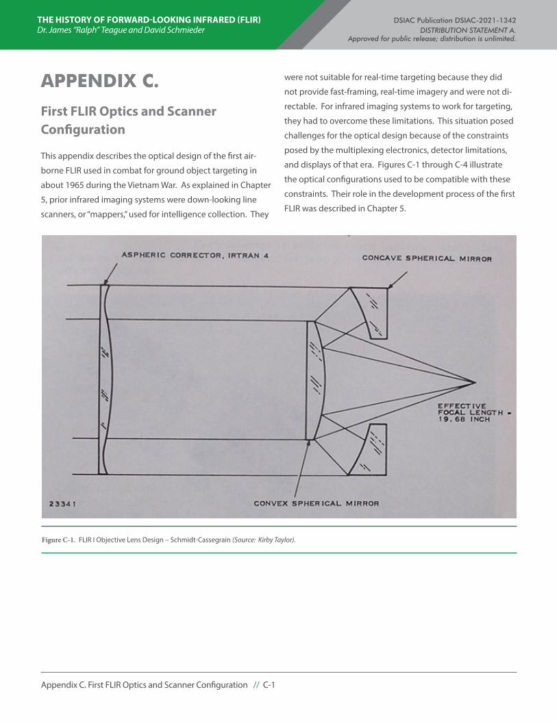
THE HISTORY OF FORWARD-LOOKING INFRARED (FLIR) DSIAC Publication DSIAC-2021-1342 Dr. James “Ralph” Teague and David Schmieder DISTRIBUTION STATEMENT A. Approved for public release; distribution is unlimited.
Appendix C. First FLIR Optics and Scanner Configuration // C-1
APPENDIX C.
First FLIR Optics and Scanner Configuration
This appendix describes the optical design of the first air-
borne FLIR used in combat for ground object targeting in
about 1965 during the Vietnam War. As explained in Chapter
5, prior infrared imaging systems were down-looking line
scanners, or “mappers,” used for intelligence collection. They
were not suitable for real-time targeting because they did
not provide fast-framing, real-time imagery and were not di-
rectable. For infrared imaging systems to work for targeting,
they had to overcome these limitations. This situation posed
challenges for the optical design because of the constraints
posed by the multiplexing electronics, detector limitations,
and displays of that era. Figures C-1 through C-4 illustrate
the optical configurations used to be compatible with these
constraints. Their role in the development process of the first
FLIR was described in Chapter 5.
Figure C-1. FLIR I Objective Lens Design – Schmidt-Cassegrain (Source: Kirby Taylor).

THE HISTORY OF FORWARD-LOOKING INFRARED (FLIR) DSIAC Publication DSIAC-2021-1342 Dr. James “Ralph” Teague and David Schmieder DISTRIBUTION STATEMENT A. Approved for public release; distribution is unlimited.
Appendix C. First FLIR Optics and Scanner Configuration // C-2
Figure C-2. FLIR I Three-Element Staggered Detector Array (Source: Kirby Taylor).
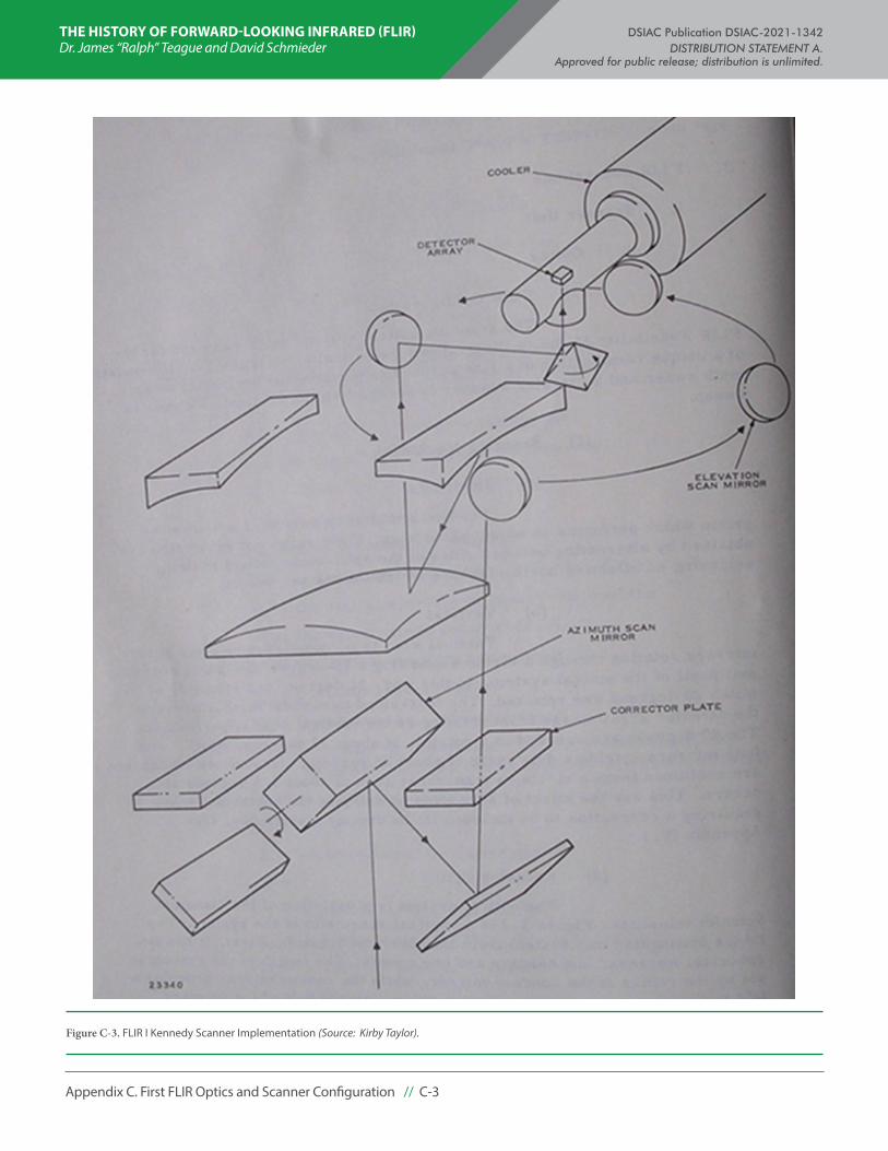
THE HISTORY OF FORWARD-LOOKING INFRARED (FLIR) DSIAC Publication DSIAC-2021-1342 Dr. James “Ralph” Teague and David Schmieder DISTRIBUTION STATEMENT A. Approved for public release; distribution is unlimited.
Appendix C. First FLIR Optics and Scanner Configuration // C-3
Figure C-3. FLIR I Kennedy Scanner Implementation (Source: Kirby Taylor).

THE HISTORY OF FORWARD-LOOKING INFRARED (FLIR) DSIAC Publication DSIAC-2021-1342 Dr. James “Ralph” Teague and David Schmieder DISTRIBUTION STATEMENT A. Approved for public release; distribution is unlimited.
Appendix C. First FLIR Optics and Scanner Configuration // C-4
Figure C-4. Kennedy 2-Axis Scanner Patent Drawing (Source: U.S. Patent 3,554,628; applied for in 1966).
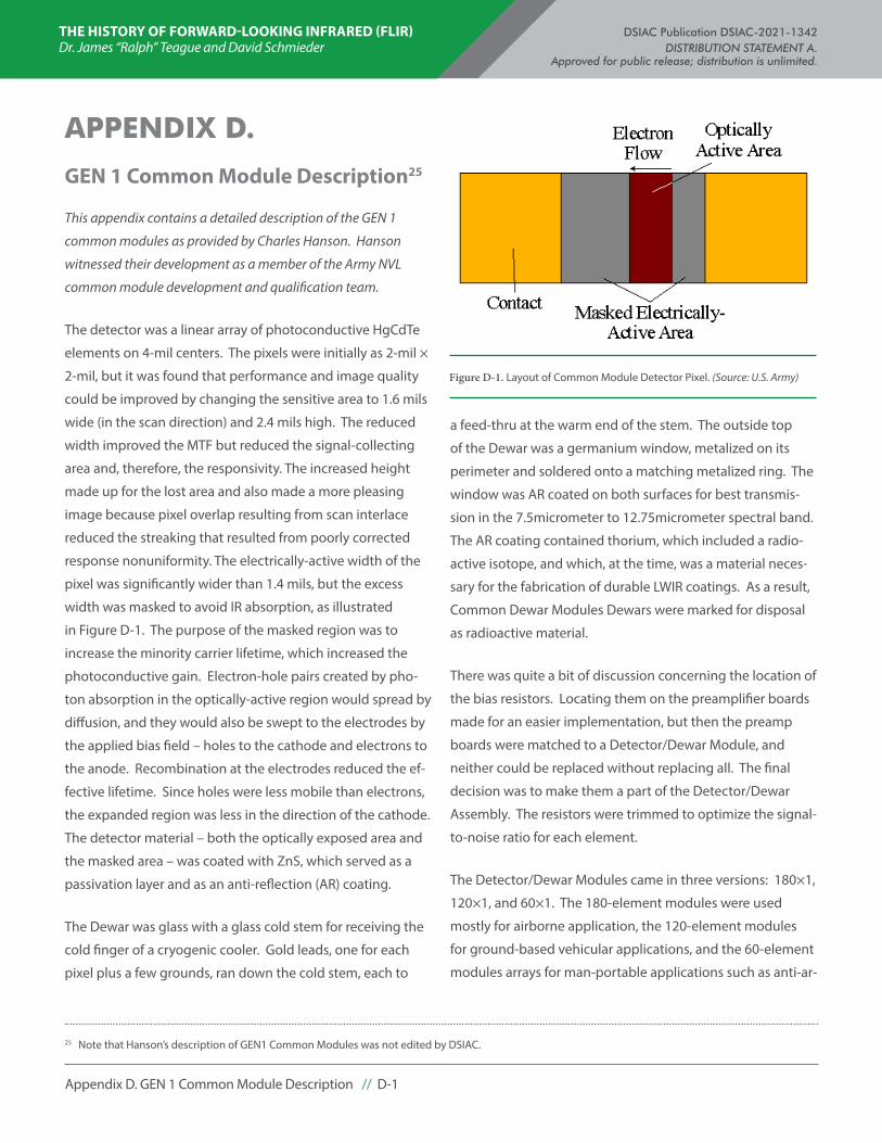
THE HISTORY OF FORWARD-LOOKING INFRARED (FLIR) DSIAC Publication DSIAC-2021-1342 Dr. James “Ralph” Teague and David Schmieder DISTRIBUTION STATEMENT A. Approved for public release; distribution is unlimited.
Appendix D. GEN 1 Common Module Description // D-1
APPENDIX D.
GEN 1 Common Module Description25
This appendix contains a detailed description of the GEN 1
common modules as provided by Charles Hanson. Hanson
witnessed their development as a member of the Army NVL
common module development and qualification team.
The detector was a linear array of photoconductive HgCdTe
elements on 4-mil centers. The pixels were initially as 2-mil ×
2-mil, but it was found that performance and image quality
could be improved by changing the sensitive area to 1.6 mils
wide (in the scan direction) and 2.4 mils high. The reduced
width improved the MTF but reduced the signal-collecting
area and, therefore, the responsivity. The increased height
made up for the lost area and also made a more pleasing
image because pixel overlap resulting from scan interlace
reduced the streaking that resulted from poorly corrected
response nonuniformity. The electrically-active width of the
pixel was significantly wider than 1.4 mils, but the excess
width was masked to avoid IR absorption, as illustrated
in Figure D-1. The purpose of the masked region was to
increase the minority carrier lifetime, which increased the
photoconductive gain. Electron-hole pairs created by pho-
ton absorption in the optically-active region would spread by
diffusion, and they would also be swept to the electrodes by
the applied bias field – holes to the cathode and electrons to
the anode. Recombination at the electrodes reduced the ef-
fective lifetime. Since holes were less mobile than electrons,
the expanded region was less in the direction of the cathode.
The detector material – both the optically exposed area and
the masked area – was coated with ZnS, which served as a
passivation layer and as an anti-reflection (AR) coating.
The Dewar was glass with a glass cold stem for receiving the
cold finger of a cryogenic cooler. Gold leads, one for each
pixel plus a few grounds, ran down the cold stem, each to
25 Note that Hanson’s description of GEN1 Common Modules was not edited by DSIAC.
a feed-thru at the warm end of the stem. The outside top
of the Dewar was a germanium window, metalized on its
perimeter and soldered onto a matching metalized ring. The
window was AR coated on both surfaces for best transmis-
sion in the 7.5micrometer to 12.75micrometer spectral band.
The AR coating contained thorium, which included a radio-
active isotope, and which, at the time, was a material neces-
sary for the fabrication of durable LWIR coatings. As a result,
Common Dewar Modules Dewars were marked for disposal
as radioactive material.
There was quite a bit of discussion concerning the location of
the bias resistors. Locating them on the preamplifier boards
made for an easier implementation, but then the preamp
boards were matched to a Detector/Dewar Module, and
neither could be replaced without replacing all. The final
decision was to make them a part of the Detector/Dewar
Assembly. The resistors were trimmed to optimize the signal-
to-noise ratio for each element.
The Detector/Dewar Modules came in three versions: 180×1,
120×1, and 60×1. The 180-element modules were used
mostly for airborne application, the 120-element modules
for ground-based vehicular applications, and the 60-element
modules arrays for man-portable applications such as anti-ar-
Figure D-1. Layout of Common Module Detector Pixel. (Source: U.S. Army)
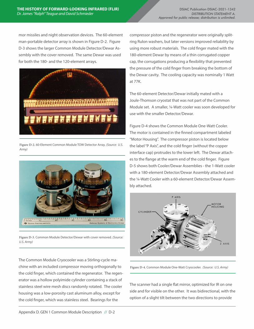
THE HISTORY OF FORWARD-LOOKING INFRARED (FLIR) DSIAC Publication DSIAC-2021-1342 Dr. James “Ralph” Teague and David Schmieder DISTRIBUTION STATEMENT A. Approved for public release; distribution is unlimited.
Appendix D. GEN 1 Common Module Description // D-2
mor missiles and night observation devices. The 60-element
man-portable detector array is shown in Figure D-2. Figure
D-3 shows the larger Common Module Detector/Dewar As-
sembly with the cover removed. The same Dewar was used
for both the 180- and the 120-element arrays.
The Common Module Cryocooler was a Stirling-cycle ma-
chine with an included compressor moving orthogonally to
the cold finger, which contained the regenerator. The regen-
erator was a hollow polyimide cylinder containing a stack of
stainless steel wire mesh discs randomly rotated. The cooler
housing was a low-porosity cast aluminum alloy, except for
the cold finger, which was stainless steel. Bearings for the
compressor piston and the regenerator were originally split-
ring Rulon washers, but later versions improved reliability by
using more robust materials. The cold finger mated with the
180-element Dewar by means of a thin corrugated copper
cap, the corrugations producing a flexibility that prevented
the pressure of the cold finger from breaking the bottom of
the Dewar cavity. The cooling capacity was nominally 1 Watt
at 77K.
The 60-element Detector/Dewar initially mated with a
Joule-Thomson cryostat that was not part of the Common
Module set. A smaller, ¼-Watt cooler was soon developed for
use with the smaller Detector/Dewar.
Figure D-4 shows the Common Module One-Watt Cooler.
The motor is contained in the finned compartment labeled
“Motor Housing”. The compressor piston is located below
the label “P Axis”, and the cold finger (without the copper
interface cap) protrudes to the lower left. The Dewar attach-
es to the flange at the warm end of the cold finger. Figure
D-5 shows both Cooler/Dewar Assemblies - the 1-Watt cooler
with a 180-element Detector/Dewar Assembly attached and
the ¼-Watt Cooler with a 60-element Detector/Dewar Assem-
bly attached.
The scanner had a single flat mirror, optimized for IR on one
side and for visible on the other. It was bidirectional, with the
option of a slight tilt between the two directions to provide
Figure D-2. 60-Element Common Module TOW Detector Array. (Source: U.S. Army)
Figure D-3. Common Module Detector/Dewar with cover removed. (Source: U.S. Army)
Figure D-4. Common Module One-Watt Cryocooler. (Source: U.S. Army)
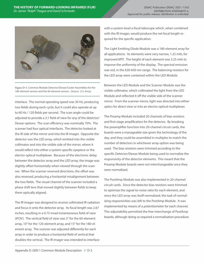
THE HISTORY OF FORWARD-LOOKING INFRARED (FLIR) DSIAC Publication DSIAC-2021-1342 Dr. James “Ralph” Teague and David Schmieder DISTRIBUTION STATEMENT A. Approved for public release; distribution is unlimited.
Appendix D. GEN 1 Common Module Description // D-3
interlace. The normal operating speed was 30 Hz, producing
two fields during each cycle, but it could also operate at up
to 60 Hz / 120 fields per second. The scan angle could be
adjusted to provide a 2:1 field of view for any of the detector/
Dewar options. The scan efficiency was nominally 70%. The
scanner had four optical interfaces. The detector looked at
the IR side of the mirror and into the IR imager. Opposite the
detector was the LED array, which emitted into the visible
collimator and into the visible side of the mirror, where it
would reflect into either a system-specific eyepiece or the
electro-optical multiplexer. Because of the electronic delay
between the detector array and the LED array, the image was
slightly offset horizontally when viewed through the scan-
ner. When the scanner reversed directions, the offset was
also reversed, producing a horizontal misalignment between
the two fields. The visual channel of the scanner included a
phase shift lens that moved slightly between fields to keep
them optically aligned.
The IR imager was designed to receive collimated IR radiation
and focus it onto the detector array. Its focal length was 2.67
inches, resulting in a 0.75 mrad instantaneous field of view
(IFOV). The vertical field of view was 5° for the 60-element
array, 10° for the 120-element array, and 15° for the 180-el-
ement array. The scanner was adjusted differently for each
array in order to produce a horizontal field of vertical that
doubles the vertical. The IR imager was intended to interface
with a system-level a-focal telescope which, when combined
with the IR imager, would produce the net focal length re-
quired for the specific application.
The Light Emitting Diode Module was a 180-element array for
all applications. Its elements were very narrow, 1.25 mils, for
improved MTF. The height of each element was 3.25 mils to
improve the uniformity of the display. The spectral emission
was red, in the 620-650 nm range. The balancing resistors for
the LED array were contained within the LED Module.
Between the LED Module and the Scanner Module was the
visible collimator, which collimated the light from the LED
Module and reflected it off the visible side of the scanner
mirror. From the scanner mirror, light was directed into either
optics for direct view or into an electro-optical multiplexer.
The Preamp Module included 20 channels of bias resistors
and first-stage amplification for the detector. By breaking
the preamplifier function into 20-channel circuit cards, the
boards were a manageable size given the technology of the
day, and they could be assembled in multiples to match the
number of detectors in whichever array option was being
used. The bias resistors were trimmed according to the
specific Detector/Dewar Module being used to normalize the
responsivity of the detector elements. This meant that the
Preamp Module boards were not interchangeable once they
were normalized.
The PostAmp Module was also implemented in 20-channel
circuit cards. Since the detector bias resistors were trimmed
to optimize the signal-to-noise ratio for each element, and
since the LED array was itself normalized, the task of normal-
izing responsivities was left to the PostAmp Module. It was
implemented by means of a potentiometer for each channel.
This adjustability permitted the free interchange of PostAmp
boards, although doing so required a normalization procedure.
Figure D-5. Common Module Detector/Dewar/Cooler Assemblies for the 180-element version and the 60-element version. (Source: U.S. Army)

THE HISTORY OF FORWARD-LOOKING INFRARED (FLIR) DSIAC Publication DSIAC-2021-1342 Dr. James “Ralph” Teague and David Schmieder DISTRIBUTION STATEMENT A. Approved for public release; distribution is unlimited.
Bibliography // E-1
BIBLIOGRAPHYBarr, E. S. “The Infrared Pioneers – I. Sir William Herschel.” Infrared
Physics, vol. 1, 1961.
Barr, E. S. “The Infrared Pioneers – II. Macedonio Melloni.” Infrared Physics, vol. 2, 1962.
Barr, E. S. “The Infrared Pioneers – III. Samuel Pierpont Langley.” Infra-red Physics, vol. 3, 1963.
California Institute of Technology. “Thermoelectrics: Caltech Materi-als Science.” http://www.thermoelectrics.caltech.edu/, accessed 4 September 2012.
Cool Cosmos. http://coolcosmos.ipac.caltech.edu, accessed 27 August 2013.
Earth Observatory. “Samuel Pierpont Langley (1834-1906).” https://earthobservatory.nasa.gov/Features/Langley/langley_2.php, 3 May 2000.
Hershel, W. The Scientific Papers of Sir William Herschel. London, England: The Royal Society and the Royal Astronomical Society of England, 1912.
Holden, E. S. Sir William Herschel His Life and Works. New York: Charles Scribner’s Sons, 1880.
Holmes, R. The Age of Wonder: The Romantic Generation and the Discovery of the Beauty and Terror of Science. New York: Harper-Collins, 2008.
Hong, G. “Thomas Johann Seebeck.” Speech and Hearing Science Historical Review, New Taipei City, Taiwan: Fu Jen Catholic Uni-versity, 2003.
Hoskin, M. “William Herschel.” New Dictionary of Scientific Biography, vol. 3, New York: Charles Scribner’s Sons, 2008.
Infrared Training Institute. “Macedonio Melloni.” https://infra-redtraininginstitute.com/infrared-thermography-history/mace-donio-melloni/, accessed 4 September 2012.
Mahidol University. “Mahidol Physics Education Centre.” Nakhon Pathom, Thailand, http://mpec.sc.mahidol.ac.th/, accessed 4 September 2012.
Millman, P. M. “The Herschel Dynasty - Part One: William Her-schel.” Journal of the Royal Astronomical Society of Canada, vol. 74, pp. 134, 1980, http://adsabs.harvard.edu/full/seri/JRASC/0074/0000134.000.html, accessed September 2012.
Mullaney, J. “Herschel’s Telescopes.” The Herschel Objects and How to Observe Them, Springer Science & Business Media, pp. 10, 2007, http://books.google.com/books?id=HFg2sOjrFtsC&pg=PA10, accessed 5 June 2011.
Redd, N. T. “William Herschel Biography.” Space.com, https://www.space.com/17432-william-herschel.html, 4 September 2012.
Rousse, D. R. “A Brief Review of the History of Radiative Transfer.” Proceedings from the Third International Conference on Thermal Engineering: Theory and Applications, 21−23 May 2007.
Steinicke, W. “‘The Scientific Papers of Sir William Herschel’ at 100.” Astronomy & Geophysics, vol. 53, no. 2, 1 April 2012.
Students for the Exploration and Development of Space (SEDS) USA. “The Messier Catalog.” http://messier.seds.org/, 25 February 2008.
Universität Innsbruck. “Melloni’s Thermo Couple, 1831.” http://physik.uibk.ac.at/museum/en/details/electr/melloni.html, accessed 4 September 2012.

THE HISTORY OF FORWARD-LOOKING INFRARED (FLIR) DSIAC Publication DSIAC-2021-1342 Dr. James “Ralph” Teague and David Schmieder DISTRIBUTION STATEMENT A. Approved for public release; distribution is unlimited.
Acronyms and Abbreviations // F-1
ACRONYMS AND ABBREVIATIONSAFAL Air Force Avionics Laboratory
AFB Air Force Base
AMC Army Materiel Command
APC Armored Personnel Carrier
APE Advanced Production Engineering
ATIRCM Advanced Threat Infrared Countermeasure
CCB Configuration Control Board
CCD Charge Coupled Device
CdTe Cadmium Telluride
CdZnTe Cadmium Zinc Telluride
CERDEC Communications-Electronics Research, Development and Engineering Center
CID Charge Injection Device
CINFAC Counterinsurgency Information Analysis Center
CMOS Complementary Metal-Oxide-Semiconductor
COTR Contracting Officer’s Technical Representative
CRT Cathode Ray Tube
CTE Coefficient of Thermal Expansion
DARPA Defense Advanced Research Projects Agency
DAS Distributed Aperture Sensor
DoD Department of Defense
DROIC Digital Read-Out Integrated Circuit
DTIC Defense Technical Information Center
EM Electromagnetic
EO Electro-Optical
ERDL Engineer Research and Development Laboratories
FFRDC Federally Funded Research & Development Center
FLIR Forward-Looking Infrared
FOV Field of View
FPA Focal Plane Array
FPN Fixed-Pattern Noise
GaAs Gallium Arsenide
GE General Electric
Ge:Hg Mercury-Doped Germanium
GEN2 Second Generation
GTPE Georgia Tech Professional Education
GTRI Georgia Tech Research Institute
HAC Hughes Aircraft Corporation
HgCdTe Mercury Cadmium Telluride
HHTV Handheld Thermal Viewer
HSI Hyperspectral Imaging
IAC Information Analysis Center
IDA Institute for Defense Analysis
IDCA Integrated Detector Dewar Assembly
IEEE Institute of Electrical and Electronics Engineers
IMH Integrated Multiplexed Hybrid
InSb Indium Antimonide
IR Infrared
IRCM Infrared Countermeasure
IRE Institute of Radio Engineers
IRIA IR Information and Analysis
IRIS Infrared Information Symposium
IRST Infrared Search and Track
JLC Joint Logistics Commanders
JOSA Journal of the Optical Society of America
JPL Jet Propulsion Laboratory
JTCG Joint Technical Coordinating Group
LED Light-Emitting Diode
LLLTV Low Light Level Television
LN2 Liquid Nitrogen
LPE Liquid Phase Epitaxy
LWIR Long-Wave Infrared
MBE Molecular Beam Epitaxy
MCT Mercury Cadmium Telluride
MIS Metal-Insulator-Semiconductor
MOCVD Metal Organic Chemical Vapor Deposition
MOSFET Metal-Oxide-Semiconductor Field Effect Transistor
THE HISTORY OF FORWARD-LOOKING INFRARED (FLIR) DSIAC Publication DSIAC-2021-1342 Dr. James “Ralph” Teague and David Schmieder DISTRIBUTION STATEMENT A. Approved for public release; distribution is unlimited.
Acronyms and Abbreviations // F-2
MRT Minimum Resolvable Temperature
MSS Military Sensing Symposia
MTADS Modern Target Acquisition and Designation Sight
MTF Modulation Transfer Function
MWIR Medium-Wave Infrared
MWR Missile Warning Receiver
Nd:YAG Neodymium-Doped Yttrium Aluminum Garnet
NET Noise Equivalent Temperature
NETD Net Equivalent Temperature Difference
NIMS Near IR Mapping Spectrometer
NIR Near Infrared
NRL Naval Research Laboratory
NUC Nonuniformity Compensation
NVESD Night Vision & Electronic Sensors Directorate
NVL Night Vision Laboratory
ONR Office of Naval Research
P3I Preplanned Product Improvement
PACE Producible Alternative to CdTe Epitaxy
PbS Lead Sulfide
PbSe Lead Selenide
PC Photoconductive
PCB Printed Circuit Board
PM Program Manager
PtSi Platinum Silicide
PV Photovoltaic
QE Quantum Efficiency
QWIP Quantum Well IR Photodetectors
RACIC Remote Areas Conflict Information Center
RCA Radio Corporation of America
RDECOM Research, Development, and Engineering Command
RF Radio Frequency
ROIC Read-Out Integrated Circuit
RRE Royal Radar Establishment
SADA Standard Advanced Dewar Assembly
SBRC Santa Barbara Research Center
SENSIAC Sensing Information Analysis Center
SOAR State-of-the-Art Report
SPIE Society of Photo-Optical Instrumentation Engineers
SPRITE Signal Processing in the Element
SWaP-C Size, Weight, Power, and Cost
SWIR Short-Wave Infrared
TDI Time Delay and Integration
TE Thermoelectric
THAAD Terminal High-Altitude Area Defense
TI Texas Instruments
Tl2S Thallous Sulfide
TOW Tube-Launched, Optically Tracked, Wire-Guided
TRAM Target Recognition and Attack Multisensor
TRIM Trails and Roads Interdiction Mission
UV Ultraviolet
VIMS Visible/IR Mapping Spectrometer
VLWIR Very Long-Wave Infrared
WWI World War I
WWII World War II
THE HISTORY OF FORWARD-LOOKING INFRARED (FLIR)By Dr. James “Ralph” Teague and David Schmieder
DSIAC PUBLICATION DSIAC-2021-1342
DISTRIBUTION STATEMENT A Approved for public release; distribution is unlimited.
Top Related