


Languages
Pages
Legal

Research ArticlePhotovoltaic and Charge Trapping Characteristics of Screen-Printed Monocrystalline Silicon Solar Cells with MolybdenumOxides as Hole-Selective Layers by H2/Ar Plasma Pretreatment
Chin-Lung Cheng , Chi-Chung Liu, and Chih-Chieh Hsu
Department of Electro-Optical Engineering, National Formosa University, Yunlin 63201, Taiwan
Correspondence should be addressed to Chin-Lung Cheng; [email protected]
Received 15 August 2020; Accepted 6 November 2020; Published 16 November 2020
Academic Editor: Alberto Álvarez-Gallegos
Copyright © 2020 Chin-Lung Cheng et al. This is an open access article distributed under the Creative Commons AttributionLicense, which permits unrestricted use, distribution, and reproduction in any medium, provided the original work isproperly cited.
Photovoltaic characteristics of screen-printedmonocrystalline silicon solar cells (SPSSCs) with molybdenum oxide (MoOx) as hole-selective layers (HSLs) were demonstrated. A H2/Ar plasma pretreatment (PPT) was incorporated into a MoOx/p-Si(100) interface,which shows the expected quality in terms of passivation. Moreover, the charge trapping characteristics of the MoOx/p-Si(100)interface were presented. The PPT parameters, including power, treated time, flow ratio of H2/Ar, and temperature, wereinvestigated. The experimental results indicate that the Si-H bond with a relatively high intensity was demonstrated for theH2/Ar PPT. The achievement of a conversion efficiency (CE) improvement of more than 1.2% absolute from 18.3% to 19.5% forSPSSCs with H2/Ar PPT was explored. The promoted mechanism was attributed to the reduction of the interface trap densitycaused by the large number of Si-H bonds at the silicon substrate and MoOx interface.
1. Introduction
Passivated emitter and rear cell (PERC) silicon solar cells arethe mainstream of the industrial solar cells today [1–3]. Toincrease the capture of photons by solar cells, PERC intro-duces two additional layers at the rear of the cell comparedwith SPSSCs [4]. The function of those layers is to improvethe passivation of the rear side and increase the reflectionof the back light [5]. However, PERC still have a smallamount of Al back surface field (Al-BSF), which will causerecombination [6]. Thus, to improve this shortcoming, tran-sition metal oxides, such as MoO2, V2O5, and WO3, are pro-posed as hole-selective layers (HSLs) [7–10]. The energyband of the p-type silicon substrate was matched with theHSL. Moreover, oxygen vacancy defects in the film can beutilized to transfer holes [11]. Therefore, the laser local open-ing and Al-BSF can be prevented.
Literatures reported that hydrogen (H2) PPT in fabricat-ing silicon heterojunction solar cells can be adopted toimprove surface atomic hydrogen coverage and avoid thegeneration of defects on the silicon substrate [12]. The H2
PPT of the Si surface can lead to improvements in minoritycarrier lifetime [13]. Moreover, the H2 PPT improves surfacepassivation compared to classical HF dip [14]. Furthermore,carbon and oxygen contamination can be removed from sil-icon surfaces by a 30 s H2 plasma treatment [15]. Thus, toenhance the interface characteristics of silicon and MoOx, aH2/Ar PPT was investigated.
2. Experimental Methods
To demonstrate the effects of H2/Ar plasma treatment onphotovoltaic characterizations of the SPSSCs, square samples(20 × 20mm2) of (100)-oriented p-type silicon wafers with1–3Ω cm and 190 ± 20μm were prepared. The texturingprocess was performed in a solution of 1.73% KOH at 83°Cfor 10min. The front emitters were formed by phosphorusdiffusion at 840°C for doping and drive-in. After single-sideedge isolation and PSG etching processes, the sheet resis-tances of the front emitters were demonstrated to be approx-imately 100 ± 10Ω/sq. For antireflection coating, a standardSiNx film with a thickness of 75 nm was deposited on the
HindawiInternational Journal of PhotoenergyVolume 2020, Article ID 8865010, 5 pageshttps://doi.org/10.1155/2020/8865010
n+-emitters using plasma-enhanced chemical vapor deposi-tion at a frequency of 13.56MHz. Next, an Ag front pastewas screen-printed on the front side of the SPSSCs and driedin an infrared belt furnace at 230°C. Then, a 6-zone industrialinfrared belt furnace was utilized to fire Ag pastes into the n-type emitters. The peak temperature and the belt speed wereset at 790°C and 508 cm/min, respectively. To protect thefront metallization of the SPSSCs, the polymer paste wasspin-cast onto the front surface of the SPSSCs at 3000 rpmand dried at 150°C for 30min. Then, the H2/Ar PPT was per-formed on the rear of the cells at power ranged from 50 to70W. The treated time was tuned from 0 to 70 s. TheH2/ðH2 + ArÞ ratio and temperature were achieved from22.2 to 66.6% and 200 to 300°C, respectively. The cell withoutH2/Ar PPT was presented as a reference. Next, all HSLs con-sist of MoOx/Ag films which were achieved by a thermallyevaporated technique. Deposition of the approximately4 nm thick MoOx films was performed by thermal evapora-tion from granules of MoO2 (99.9% purity). The thicknessesof evaporated Ag were 500nm. The CEs of the SPSSCs weremeasured under standard test conditions (AM 1.5G spec-trum, 100mW/cm2, 25°C). The cross-section images and ele-mental analysis of p-Si(100)/MoOx/Ag were examined bytransmission electron microscopy (TEM) and energy-dispersive X-ray spectroscopy (EDS), respectively. The Si-Hbonds of the H2/Ar PPT samples were measured usingFourier-transform infrared spectroscopy (FTIR).
3. Results and Discussion
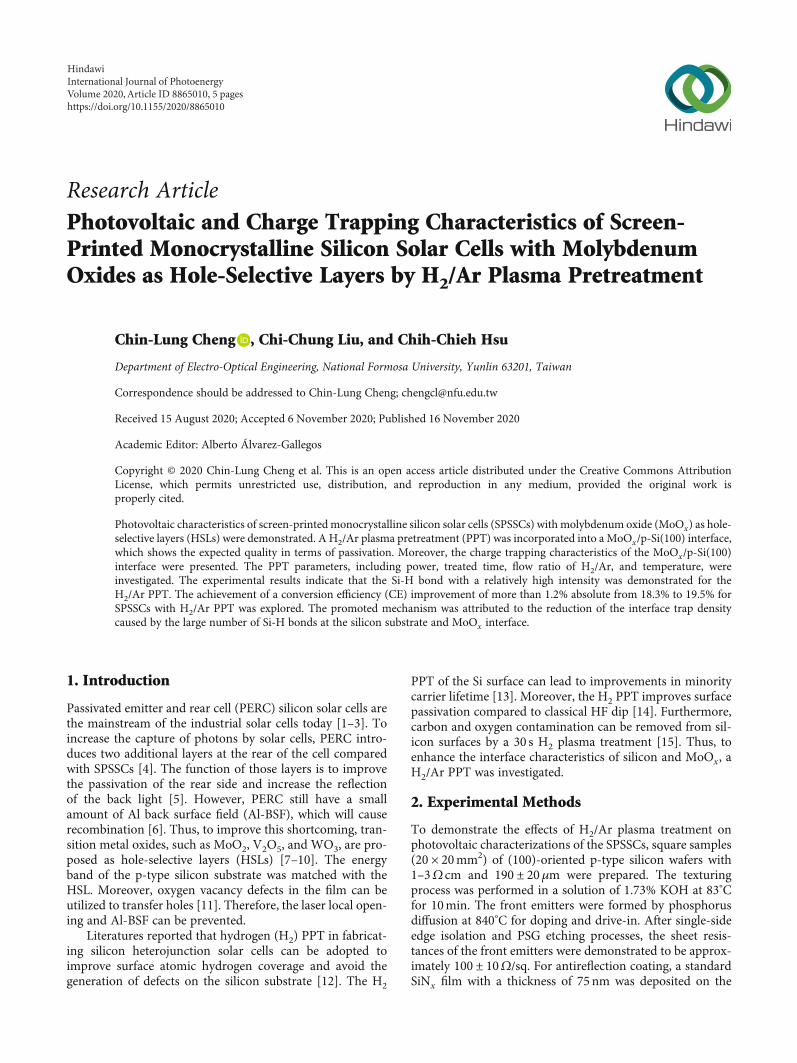
The cross-section image and elemental analysis of p-Si(100)/MoOx/Ag stacked films were examined by the TEMand EDS with a line drawn as shown in Figure 1. The thick-nesses of the MoOx HSLs and SiOx were demonstrated to beapproximately 4 and 1.8 nm, respectively. The SiOx interfa-
cial layer is present at the MoOx/Si(100) interface duringMoOx evaporation [16]. Elemental analysis of the p-Si(100)/SiOx/MoOx/Ag stacked films by EDS is shown inFigure 1(b). The MoOx were thermally evaporated at a basepressure of 5 × 10⁻⁶ Torr. The Mo/O atomic ratio in theMoOx layers was approximately 1/2.3 for the MoO2 sourcegranules. Literature reported that the Mo+4, Mo+5, or Mo+6
states could be presented in MoOx HSL [17]. In this work,the O/Mo atomic ratio of 2.3 in the MoOx HSLs for theMoO2 granule source was attributed to some oxygen alreadybeing in the chamber during evaporation [16].
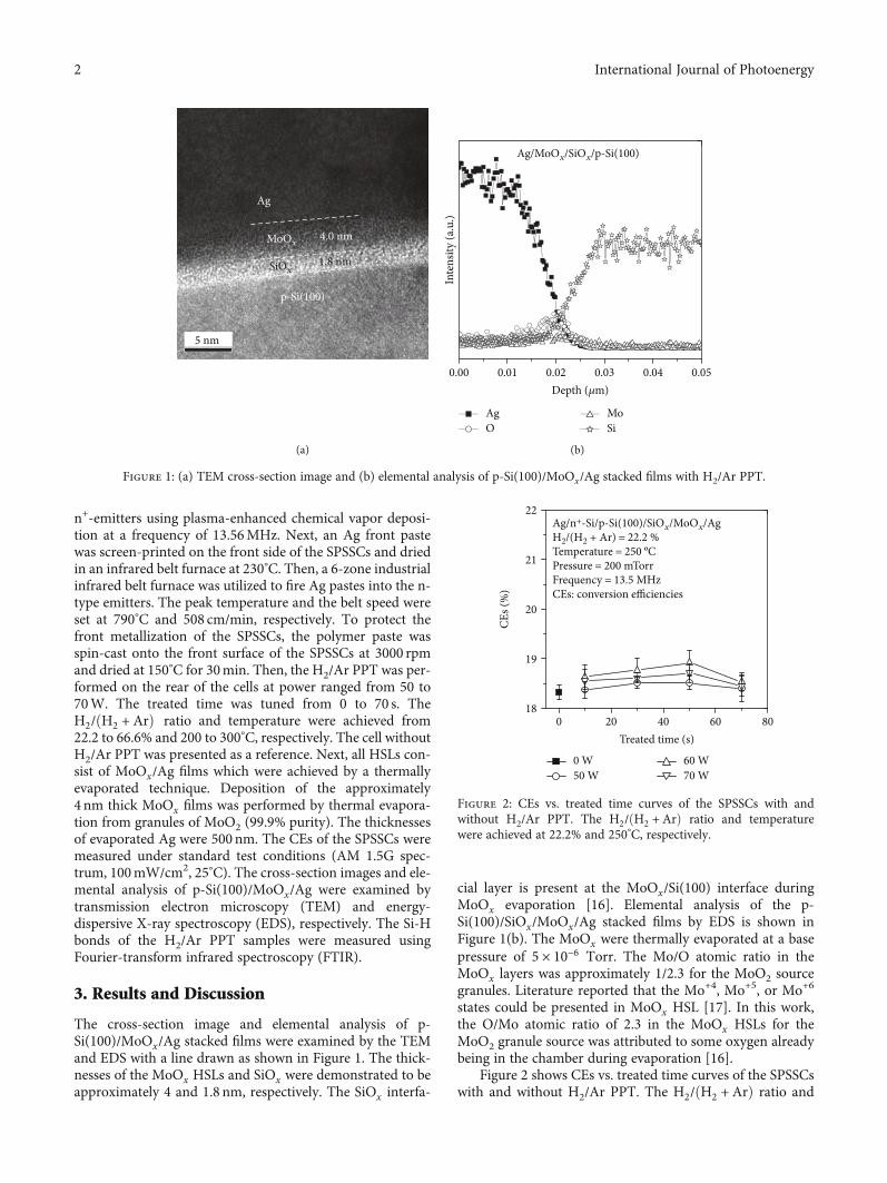
Figure 2 shows CEs vs. treated time curves of the SPSSCswith and without H2/Ar PPT. The H2/ðH2 + ArÞ ratio and
5 nm
Ag
MoOx
p-Si(100)
4.0 nm
SiOx1.8 nm
(a)
0.00 0.01 0.02 0.03
Ag/MoOx/SiOx/p-Si(100)
AgO
MoSi
Depth (𝜇m)
Inte
nsity
(a.u
.)
0.04 0.05
(b)
Figure 1: (a) TEM cross-section image and (b) elemental analysis of p-Si(100)/MoOx/Ag stacked films with H2/Ar PPT.
Ag/n+-Si/p-Si(100)/SiOx/MoOx/AgH2/(H2 + Ar) = 22.2 %Temperature = 250 CPressure = 200 mTorrFrequency = 13.5 MHzCEs: conversion efficiencies
018
19
CEs (
%)
20
21
22
20 40
0 W50 W
60 W70 W
Treated time (s)60 80
Figure 2: CEs vs. treated time curves of the SPSSCs with andwithout H2/Ar PPT. The H2/ðH2 + ArÞ ratio and temperaturewere achieved at 22.2% and 250°C, respectively.
2 International Journal of Photoenergy
temperature were achieved at 22.2% and 250°C, respectively.The CE was enhanced by increasing the treated time. How-ever, an excess of treated time could cause a degradation ofthe CE due to the increase of dangling bond defects on thesurface, which can result in etching effects of the H2 plasma[12]. Compared with various powers and treated time, a bet-ter CE improvement was demonstrated at a power of 60Wfor 50 s. The achievement of a CE improvement of more than0.6% absolute from 18.3% to 18.9% for SPSSCs with andwithout H2/Ar PPT was explored.
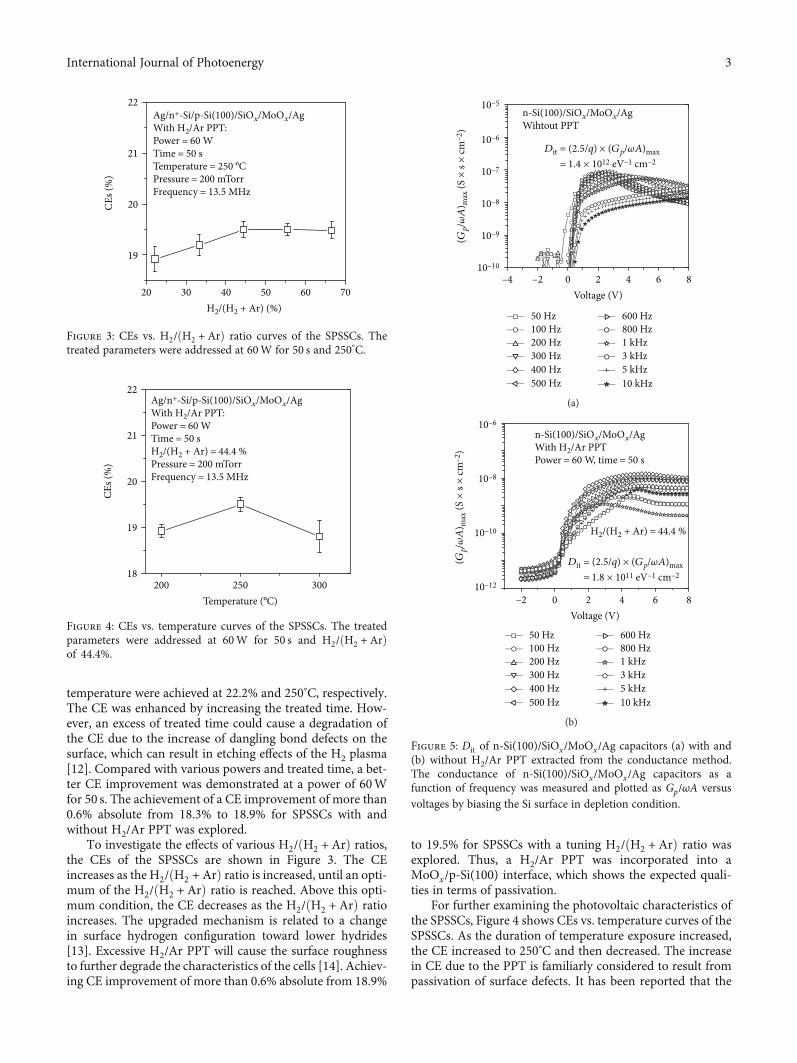
To investigate the effects of various H2/ðH2 + ArÞ ratios,the CEs of the SPSSCs are shown in Figure 3. The CEincreases as theH2/ðH2 + ArÞ ratio is increased, until an opti-mum of the H2/ðH2 + ArÞ ratio is reached. Above this opti-mum condition, the CE decreases as the H2/ðH2 + ArÞ ratioincreases. The upgraded mechanism is related to a changein surface hydrogen configuration toward lower hydrides[13]. Excessive H2/Ar PPT will cause the surface roughnessto further degrade the characteristics of the cells [14]. Achiev-ing CE improvement of more than 0.6% absolute from 18.9%
to 19.5% for SPSSCs with a tuning H2/ðH2 + ArÞ ratio wasexplored. Thus, a H2/Ar PPT was incorporated into aMoOx/p-Si(100) interface, which shows the expected quali-ties in terms of passivation.
For further examining the photovoltaic characteristics ofthe SPSSCs, Figure 4 shows CEs vs. temperature curves of theSPSSCs. As the duration of temperature exposure increased,the CE increased to 250°C and then decreased. The increasein CE due to the PPT is familiarly considered to result frompassivation of surface defects. It has been reported that the
Ag/n+-Si/p-Si(100)/SiOx/MoOx/AgWith H2/Ar PPT:Power = 60 WTime = 50 sTemperature = 250 CPressure = 200 mTorrFrequency = 13.5 MHz
19
CEs (
%)
20
21
22
20 30 40H2/(H2 + Ar) (%)
50 60 70
Figure 3: CEs vs. H2/ðH2 + ArÞ ratio curves of the SPSSCs. Thetreated parameters were addressed at 60W for 50 s and 250°C.
Ag/n+-Si/p-Si(100)/SiOx/MoOx/AgWith H2/Ar PPT:Power = 60 WTime = 50 sH2/(H2 + Ar) = 44.4 %Pressure = 200 mTorrFrequency = 13.5 MHz
19
18
CEs (
%)
20
21
22
200 250Temperature (ºC)
300
Figure 4: CEs vs. temperature curves of the SPSSCs. The treatedparameters were addressed at 60W for 50 s and H2/ðH2 + ArÞof 44.4%.
Dit = (2.5/q) (Gp/𝜔A)max= 1.4 1012 eV–1 cm–2
50 Hz100 Hz200 Hz300 Hz400 Hz500 Hz
600 Hz800 Hz1 kHz3 kHz5 kHz10 kHz
n-Si(100)/SiOx/MoOx/AgWihtout PPT
10–10
–4 –2 0 2Voltage (V)
4 6 8
10–9
10–8
(Gp/𝜔A
) max
(S
cm–2
)
10–7
10–6
10–5
(a)
Dit = (2.5/q) (Gp/𝜔A)max= 1.8 × 10¹¹ eV–1 cm–2
50 Hz100 Hz200 Hz300 Hz400 Hz500 Hz
H2/(H2 + Ar) = 44.4 %
600 Hz800 Hz1 kHz3 kHz5 kHz10 kHz
n-Si(100)/SiOx/MoOx/AgWith H2/Ar PPTPower = 60 W, time = 50 s
–2 0 2Voltage (V)
4 6 810–12
10–10
10–8
10–6
(Gp/𝜔A
) max
(S ×
s ×
cm–2
)
(b)
Figure 5: Dit of n-Si(100)/SiOx/MoOx/Ag capacitors (a) with and(b) without H2/Ar PPT extracted from the conductance method.The conductance of n-Si(100)/SiOx/MoOx/Ag capacitors as afunction of frequency was measured and plotted as Gp/ωA versusvoltages by biasing the Si surface in depletion condition.
3International Journal of Photoenergy
smaller effective surface recombination velocity can beachieved by the higher deposition temperature [14]. Theresults indicate that the best result in this work is a CE of19.5% at deposition temperature ranging from 250 to 300°C.
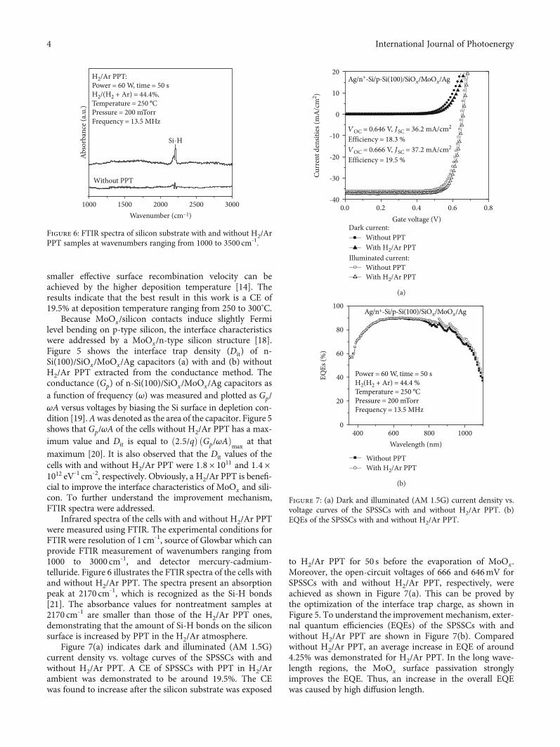
Because MoOx/silicon contacts induce slightly Fermilevel bending on p-type silicon, the interface characteristicswere addressed by a MoOx/n-type silicon structure [18].Figure 5 shows the interface trap density (Dit) of n-Si(100)/SiOx/MoOx/Ag capacitors (a) with and (b) withoutH2/Ar PPT extracted from the conductance method. Theconductance (Gp) of n-Si(100)/SiOx/MoOx/Ag capacitors asa function of frequency (ω) was measured and plotted as Gp/ωA versus voltages by biasing the Si surface in depletion con-dition [19].Awas denoted as the area of the capacitor. Figure 5shows that Gp/ωA of the cells without H2/Ar PPT has a max-imum value and Dit is equal to ð2:5/qÞ ðGp/ωAÞmax at thatmaximum [20]. It is also observed that the Dit values of thecells with and without H2/Ar PPT were 1:8 × 10¹¹ and 1:4 ×10¹² eV-1 cm-2, respectively. Obviously, a H2/Ar PPT is benefi-cial to improve the interface characteristics of MoOx and sili-con. To further understand the improvement mechanism,FTIR spectra were addressed.
Infrared spectra of the cells with and without H2/Ar PPTwere measured using FTIR. The experimental conditions forFTIR were resolution of 1 cm-1, source of Glowbar which canprovide FTIR measurement of wavenumbers ranging from1000 to 3000 cm-1, and detector mercury-cadmium-telluride. Figure 6 illustrates the FTIR spectra of the cells withand without H2/Ar PPT. The spectra present an absorptionpeak at 2170 cm-1, which is recognized as the Si-H bonds[21]. The absorbance values for nontreatment samples at2170 cm-1 are smaller than those of the H2/Ar PPT ones,demonstrating that the amount of Si-H bonds on the siliconsurface is increased by PPT in the H2/Ar atmosphere.
Figure 7(a) indicates dark and illuminated (AM 1.5G)current density vs. voltage curves of the SPSSCs with andwithout H2/Ar PPT. A CE of SPSSCs with PPT in H2/Arambient was demonstrated to be around 19.5%. The CEwas found to increase after the silicon substrate was exposed
to H2/Ar PPT for 50 s before the evaporation of MoOx.Moreover, the open-circuit voltages of 666 and 646mV forSPSSCs with and without H2/Ar PPT, respectively, wereachieved as shown in Figure 7(a). This can be proved bythe optimization of the interface trap charge, as shown inFigure 5. To understand the improvement mechanism, exter-nal quantum efficiencies (EQEs) of the SPSSCs with andwithout H2/Ar PPT are shown in Figure 7(b). Comparedwithout H2/Ar PPT, an average increase in EQE of around4.25% was demonstrated for H2/Ar PPT. In the long wave-length regions, the MoOx surface passivation stronglyimproves the EQE. Thus, an increase in the overall EQEwas caused by high diffusion length.
1000
Abso
rban
ce (a
.u.)
1500 2000 2500 3000
Si-H
H2/Ar PPT:Power = 60 W, time = 50 sH2/(H2 + Ar) = 44.4%,Temperature = 250 CPressure = 200 mTorrFrequency = 13.5 MHz
Without PPT
Wavenumber (cm–1)
Figure 6: FTIR spectra of silicon substrate with and without H2/ArPPT samples at wavenumbers ranging from 1000 to 3500 cm-1.
0.0 0.2 0.4 0.6 0.8-40
Curr
ent d
ensit
ies (
mA
/cm
2 )
-30
-20
-10
0
10
20
Gate voltage (V)
VOC = 0.646 V, JSC = 36.2 mA/cm2
Efficiency = 18.3 %VOC = 0.666 V, JSC = 37.2 mA/cm2
Efficiency = 19.5 %
Dark current:Without PPTWith H2/Ar PPT
Illuminated current:Without PPTWith H2/Ar PPT
Ag/n+-Si/p-Si(100)/SiOx/MoOx/Ag
(a)
Without PPTWith H2/Ar PPT
400
EQEs
(%)
600 800 10000
20
40
60
80
100
Wavelength (nm)
Ag/n+-Si/p-Si(100)/SiOx/MoOx/Ag
Power = 60 W, time = 50 sH2(H2 + Ar) = 44.4 %Temperature = 250 CPressure = 200 mTorrFrequency = 13.5 MHz
(b)
Figure 7: (a) Dark and illuminated (AM 1.5G) current density vs.voltage curves of the SPSSCs with and without H2/Ar PPT. (b)EQEs of the SPSSCs with and without H2/Ar PPT.
4 International Journal of Photoenergy
4. Conclusions
A H2/Ar PPT process was applied to monocrystalline siliconsubstrate before depositing the MoOx HSLs. The enhancedpassivation effects of H2/Ar PPT were investigated by usinga conductance method of measuringDit, in combination withFTIR spectroscopy. The achievement of a CE improvementof more than 1.2% absolute from 18.3% to 19.5% for SPSSCswith H2/Ar PPT was explored. The promoted mechanismcould be attributed to the reduction of Dit and the increaseof the Si-H bonds at MoOx and Si substrate.
Data Availability
The data used to support the findings of this study are avail-able from the corresponding author upon request.
Conflicts of Interest
The authors declare that they have no conflicts of interest.
Acknowledgments
The authors would like to thank the Ministry of Science andTechnology of the Republic of China for the financial supportunder Contract No. MOST 108-2221-E-150-009.
References
[1] N. E. Grant, J. R. Scowcroft, A. I. Pointon, M. Al-Amin, P. P.Altermatt, and J. D. Murphy, “Lifetime instabilities in galliumdoped monocrystalline PERC silicon solar cells,” Solar EnergyMaterials and Solar Cells, vol. 206, article 110299, 2020.
[2] C. B. Mo, S. Park, S. Bae et al., “Minimizing light-induced deg-radation of the Al2O3Rear passivation layer for highly efficientPERC solar cells,” ECS Journal of Solid State Science Technol-ogy, vol. 7, no. 12, pp. Q253–Q258, 2018.
[3] J. Liu, Y. Yao, S. Xiao, and X. Gu, “Review of status develop-ments of high-efficiency crystalline silicon solar cells,” Journalof Physics D: Applied Physics, vol. 51, no. 12, p. 123001, 2018.
[4] A. To, W. Min Li, X. Li, and B. Hoex, “The effects of bifacialdeposition of ALD AlOx on the contact properties of screen-printed contacts for p-type PERC solar cells,” Energy Procedia,vol. 124, pp. 914–921, 2017.
[5] A. Uruena, L. Tous, F. Duerinckx et al., “Understanding themechanisms of rear reflectance losses in PERC type siliconsolar cells,” Energy Procedia, vol. 38, pp. 801–806, 2013.
[6] J. S. Chiu, Y. M. Zhao, S. Zhang, and D. S. Wuu, “The role oflaser ablated backside contact pattern in efficiency improve-ment of mono crystalline silicon PERC solar cells,” SolarEnergy, vol. 196, pp. 462–467, 2020.
[7] C. W. Chu, S. H. Li, C. W. Chen, V. Shrotriya, and Y. Yang,“High-performance organic thin-film transistors with metaloxide/metal bilayer electrode,” Applied Physics Letters,vol. 87, no. 19, article 193508, 2005.
[8] L. Fang, S. J. Baik, and K. S. Lim, “Transition metal oxide win-dow layer in thin film amorphous silicon solar cells,” ThinSolid Films, vol. 556, pp. 515–519, 2014.
[9] L. G. Gerling, S. Mahato, A. Morales-Vilches et al., “Transitionmetal oxides as hole-selective contacts in silicon heterojunc-
tions solar cells,” Solar Energy Materials and Solar Cells,vol. 145, pp. 109–115, 2016.
[10] C. L. Cheng, C. C. Liu, Y. S. Chiu, P. W. Chen, and Z. Y. Liu,“Air ambient and composition effects of molybdenum oxideson photovoltaic and physical characteristics of screen-printedmono-crystalline silicon solar cells,” Materials Letters,vol. 234, pp. 319–322, 2019.
[11] A. L. Fernandes Cauduro, Z. E. Fabrim, M. Ahmadpour et al.,“Tuning the optoelectronic properties of amorphous MoOx-films by reactive sputtering,” Applied Physics Letters, vol. 106,no. 20, article 202101, 2015.
[12] F. Wang, X. Zhang, L. Wang et al., “Role of hydrogen plasmapretreatment in improving passivation of the silicon surfacefor solar cells applications,” ACS Applied Material Interfaces,vol. 6, no. 17, pp. 15098–15104, 2014.
[13] S. N. Granata, T. Bearda, F. Dross, I. Gordon, J. Poortmans,and R. Mertens, “Effect of an in-situ H2 plasma pretreatmenton the minority carrier lifetime of a-Si:H(i) passivated crystal-line silicon,” Energy Procedia, vol. 27, pp. 412–418, 2012.
[14] I. Martın, M. Vetter, A. Orpella et al., “Improvement of crystal-line silicon surface passivation by hydrogen plasma treat-ment,” Applied Physics Letters, vol. 84, no. 9, pp. 1474–1476,2004.
[15] R. E. Thomas, M. J. Mantini, R. A. Rudder, D. P. Malta, S. V.Hattangady, and R. J. Markunas, “Carbon and oxygen removalfrom silicon (100) surfaces by remote plasma cleaning tech-niques,” Journal of Vacuum Science & Technology A: Vacuum,Surfaces, and Films, vol. 10, no. 4, pp. 817–822, 1992.
[16] C. L. Cheng, C. C. Liu, and Y. W. Shen, “Photovoltaic andcharge trapping characteristics of multilayer silver embeddedin molybdenum oxides as hole-selective layers for screen-printed monocrystalline silicon solar cell applications,” Jour-nal of Vacuum Science Technology B, vol. 38, no. 2, article020602, 2020.
[17] C. T. Lin, C. H. Yeh, M. H. Chen, S. H. Hsu, C. I. Wu, andT. W. Pi, “Influences of evaporation temperature on electronicstructures and electrical properties of molybdenum oxide inorganic light emitting devices,” Journal Applied Physics,vol. 107, no. 5, article 053703, 2010.
[18] S. Li, Z. Yao, J. Zhou, R. Zhang, and H. Shen, “Fabrication andcharacterization of WO3 thin films on silicon surface by ther-mal evaporation,” Materials Letters, vol. 195, pp. 213–216,2017.
[19] C. L. Cheng, K. S. Chang-Liao, and T. K.Wang, “Improvementon the electrical characteristics of HfO[sub x]N[sub y]-gatedmetal-oxide-semiconductor devices by high-temperatureannealing,” Electrochemical Solid-State Letters, vol. 9, no. 11,pp. F80–F82, 2006.
[20] E. H. Nicollian and J. R. Brews,MOS (metal oxide semiconduc-tor) physics and technology, Wiley, New York, 1982.
[21] K. O. Bugaev, A. A. Zelenina, and V. A. Volodin, “Vibrationalspectroscopy of chemical species in silicon and silicon-richnitride thin films,” International Journal of Spectroscopy,vol. 2012, Article ID 281851, 5 pages, 2012.
5International Journal of Photoenergy
Top Related