Ray optical light trapping in silicon n intensity limit · Ray optical light trapping in silicon...
16
Ray optical light trapping in silicon microwires: exceeding the 2n 2 intensity limit Emily D. Kosten, 1 Emily L. Warren, 2 and Harry A. Atwater 1,3,∗ 1 Thomas J. Watson Laboratories of Applied Physics, California Institute of Technology, Pasadena, California 91125, USA 2 Division of Chemistry and Chemical Engineering, California Institute of Technology, Pasadena, California 91125, USA 3 Kavli Nanoscience Institute, California Institute of Technology, Pasadena, California 91125, USA *[email protected] Abstract: We develop a ray optics model of a silicon wire array geometry in an attempt to understand the very strong absorption previously observed experimentally in these arrays. Our model successfully reproduces the n 2 ergodic limit for wire arrays in free space. Applying this model to a wire array on a Lambertian back reflector, we find an asymptotic increase in light trapping for low filling fractions. In this case, the Lambertian back reflector is acting as a wide acceptance angle concentrator, allowing the array to exceed the ergodic limit in the ray optics regime. While this leads to increased power per volume of silicon, it gives reduced power per unit area of wire array, owing to reduced silicon volume at low filling fractions. Upon comparison with silicon microwire experimental data, our ray optics model gives reasonable agreement with large wire arrays (4 μ m radius), but poor agreement with small wire arrays (1 μ m radius). This suggests that the very strong absorption observed in small wire arrays, which is not observed in large wire arrays, may be significantly due to wave optical effects. © 2011 Optical Society of America OCIS codes: (080.0080) Geometric optics; (350.6050) Solar energy; (000.6590) Statistical mechanics; (030.5630) Radiometry; (260.6970) Total internal reflection. References and links 1. M. Kelzenberg, S. Boettcher, J. Petykiewicz, D. Turner-Evans, M. Putnam, E. Warren, J. Spurgeon, R. Briggs, N. Lewis, and H. Atwater, “Enhanced absorption and carrier collection in si wire arrays for photovoltaic appli- cations,” Nat. Mater. 9, 239–244 (2010). 2. E. Garnett and P. Yang, “Light trapping in silicon nanowire solar cells,” Nano Lett. 10, 1082–1087 (2010). 3. L. Tsakalakos, J. Balch, J. Fronheiser, M. Shih, S. LaBoeuf, M. Pietrzykowski, P. Codella, B. Korevaar, O. Sulima, J. Rand, A. Davuluru, and U. Ropol, “Strong broadband absorption in silicon nanowire arrays with a large lattice constant for photovoltaic applications,” J. Nanophoton. 1, 013552 (2007). 4. B. Tian, X. Zheng, T. Kempa, Y. Fang, J. Huang, and C. Lieber, “Coaxial silicon nanowires as solar cells and nanoelectronic power sources,” Nature 449, 885–889 (2007). 5. E. Garnett and P. Yang, “Silicon nanowire radial p-n junction solar cells,” J. Am. Chem. Soc. 130, 9224–9225 (2008). 6. B. Kayes, H. Atwater, and N. Lewis, “Comparison of the device physics principles of planar and radial p-n junction nanorod solar cells,” J. Appl. Phys. 7, 114302–114311 (2005). 7. M. Putnam, S. Boettcher, M. Kelzenberg, D. Turner-Evans, J. Spurgeon, E. Warren, R. Briggs, N. Lewis, and H. Atwater, “Si microwire-array solar cells,” Energy Environ. Sci. 3, 1037–1041 (2010). #138520 - $15.00 USD Received 22 Nov 2010; accepted 25 Jan 2011; published 4 Feb 2011 (C) 2011 OSA 14 February 2011 / Vol. 19, No. 4 / OPTICS EXPRESS 3316
Transcript of Ray optical light trapping in silicon n intensity limit · Ray optical light trapping in silicon...

Ray optical light trapping in siliconmicrowires: exceeding the 2n2 intensity
limit
Emily D. Kosten,1 Emily L. Warren,2 and Harry A. Atwater1,3,∗1Thomas J. Watson Laboratories of Applied Physics, California Institute of Technology,
Pasadena, California 91125, USA2Division of Chemistry and Chemical Engineering, California Institute of Technology,
Pasadena, California 91125, USA3Kavli Nanoscience Institute, California Institute of Technology,
Pasadena, California 91125, USA
Abstract: We develop a ray optics model of a silicon wire array geometryin an attempt to understand the very strong absorption previously observedexperimentally in these arrays. Our model successfully reproduces the n2
ergodic limit for wire arrays in free space. Applying this model to a wirearray on a Lambertian back reflector, we find an asymptotic increase inlight trapping for low filling fractions. In this case, the Lambertian backreflector is acting as a wide acceptance angle concentrator, allowing thearray to exceed the ergodic limit in the ray optics regime. While this leadsto increased power per volume of silicon, it gives reduced power per unitarea of wire array, owing to reduced silicon volume at low filling fractions.Upon comparison with silicon microwire experimental data, our ray opticsmodel gives reasonable agreement with large wire arrays (4 μm radius), butpoor agreement with small wire arrays (1 μm radius). This suggests that thevery strong absorption observed in small wire arrays, which is not observedin large wire arrays, may be significantly due to wave optical effects.
© 2011 Optical Society of America
OCIS codes: (080.0080) Geometric optics; (350.6050) Solar energy; (000.6590) Statisticalmechanics; (030.5630) Radiometry; (260.6970) Total internal reflection.
References and links1. M. Kelzenberg, S. Boettcher, J. Petykiewicz, D. Turner-Evans, M. Putnam, E. Warren, J. Spurgeon, R. Briggs,
N. Lewis, and H. Atwater, “Enhanced absorption and carrier collection in si wire arrays for photovoltaic appli-cations,” Nat. Mater. 9, 239–244 (2010).
2. E. Garnett and P. Yang, “Light trapping in silicon nanowire solar cells,” Nano Lett. 10, 1082–1087 (2010).3. L. Tsakalakos, J. Balch, J. Fronheiser, M. Shih, S. LaBoeuf, M. Pietrzykowski, P. Codella, B. Korevaar,
O. Sulima, J. Rand, A. Davuluru, and U. Ropol, “Strong broadband absorption in silicon nanowire arrays with alarge lattice constant for photovoltaic applications,” J. Nanophoton. 1, 013552 (2007).
4. B. Tian, X. Zheng, T. Kempa, Y. Fang, J. Huang, and C. Lieber, “Coaxial silicon nanowires as solar cells andnanoelectronic power sources,” Nature 449, 885–889 (2007).
5. E. Garnett and P. Yang, “Silicon nanowire radial p-n junction solar cells,” J. Am. Chem. Soc. 130, 9224–9225(2008).
6. B. Kayes, H. Atwater, and N. Lewis, “Comparison of the device physics principles of planar and radial p-njunction nanorod solar cells,” J. Appl. Phys. 7, 114302–114311 (2005).
7. M. Putnam, S. Boettcher, M. Kelzenberg, D. Turner-Evans, J. Spurgeon, E. Warren, R. Briggs, N. Lewis, andH. Atwater, “Si microwire-array solar cells,” Energy Environ. Sci. 3, 1037–1041 (2010).
#138520 - $15.00 USD Received 22 Nov 2010; accepted 25 Jan 2011; published 4 Feb 2011(C) 2011 OSA 14 February 2011 / Vol. 19, No. 4 / OPTICS EXPRESS 3316
8. L. Hu and G. Chen, “Analysis of optical absorption in silicon nanowire arrays for photovoltaic applications,”Nano Lett. 7, 3249–3252 (2007).
9. C. Kenrick, H. Yoon, Y. Yuwen, G. Barber, H. Shen, T. Mallouk, E. Dickey, T. Mayer, and J. Redwing, “Radialjunction silicon wire array solar cells fabricated by gold-catalyzed vapor-liquid-solid growth,” Appl. Phys. Lett.97, 143108 (2010).
10. K. Peng and S. Lee, “Silicon nanowires for photovoltaic solar energy conversion,” Adv. Mater. 20, 1–18 (2010).11. O. Gunawan, K. Wang, B. Fallahazad, Y. Zhang, E. Tutuc, and S. Guha, “High performance wire-array silicon
solar cells,” Prog. Photovolt. Res. Appl. 10, 1002 (2010).12. J. Zhu, Z. Yu, G. Burkhard, C. Hsu, S. Connor, Y. Xu, Q. Wang, M. McGehee, S. Fan, and Y. Cui, “Optical
absorption enhancement in amorphous silicon nanowire and nanocone arrays,” Nano Lett. 9, 279–282 (2009).13. C. Lin and M. Povinelli, “Optical absorption enhancement in silicon nanowire arrays with a large lattice constant
for photovoltaic applications,” Nano Lett. 7, 3249–3252 (2007).14. E. Yablonovitch, “Statistical ray optics,” J. Opt. Soc. Am. 72(7), 899–907 (1982).15. M. Putnam, D. Turner-Evans, M. Kelzenberg, S. Boettcher, N. Lewis, and H. Atwater, “10 μm minority-carrier
diffusion lengths in si wire synthesized by cu-catalyzed vapor-liquid-solid growth,” Appl. Phys. Lett. 95, 163116(2009).
16. M. Born and E. Wolf, Principles of Optics, 7th Ed. (Cambridge University Press, 1999).17. We find our model very slightly exceeds the ergodic limit across all aspect ratios for the smallest filling fraction.
This is observed across aspect ratios, with no trend with increasing aspect ratios. The maximum amount by whichthe ergodic limit is exceeded is approximately 1% and is likely due to small inaccuracies in the model.
18. This should not be confused with the areal filling fraction of the wire array. In solar cells, the power can becalculated by multiplying the short circuit current, the open circuit voltage, and the fill factor, where the fillfactor accounts for the fact that the current-voltage curve is not square in the power-producing region.
19. K. Plass, M. Filler, J. Spurgeon, B. Kayes, S. Maldonado, B. Brunschwig, H. Atwater, and N. Lewis, “Flexiblepolymer-embedded si wire arrays,” Adv. Mater. 21, 325–328 (2009).
20. C. Bohren and D. Huffman, Absorption and Scattering of Light by Small Particles (Wiley-VCH, 2004).
1. Introduction
Silicon nanowire and microwire arrays have attracted significant interest as an alternative totraditional wafer-based technologies for solar cell applications [1–12] . Originally, this intereststemmed from the device physics advantages of a radial junction, which allows for the decou-pling of the absorption length from the carrier collection length. In a planar cell, both of theselengths correspond to the thickness of the cell, and high quality material is necessary so that thecell can absorb most of the light while successfully collecting the carriers. In contrast, a radialjunction offers the possibility of using lower quality, lower cost materials without sacrificingperformance [5,6]. More recently, such arrays have been found to exhibit significant light trap-ping and absorption properties [1–3], and this absorption has been modeled using the transfermatrix formalism in the nanowire regime [8, 13].
Enhancing the light trapping and absorption within a solar cell leads to increased produc-tion of electron hole pairs, and a corresponding increase in short circuit current. Light trappingschemes, such as texturing, are particularly important in the case of silicon and other low ab-sorbing materials. For textured planar substrates in the ray optics regime the light trapping limitunder isotropic illumination will be referred to here as the ergodic limit. In this limit, the in-tensity of light inside the substrate is n2 times the intensity of light incident upon the substrate,or 2n2 for the case of a back-reflector, where n is the index of refraction for the substrate. Thiseffect is due to the randomizing effect of the texturing and total internal reflection [14]. Somevery recent experimental results have suggested that nano and microwire arrays can exceed theergodic limit [1, 2]. To explore this further, we follow the approach used to derive the ergodiclimit in the planar case to find the expected light trapping and absorption for wires in the rayoptics limit. This allows us to compare to the ergodic limit and consider wires of a differentscale than those considered in previously.
While much of the previous work has been done with nanowires in the subwavelengthregime, far below the ray optics limit, large diameter microwires can be grown by vapor-liquid-solid (VLS) techniques [1]. Previous device physics modeling suggests that for efficient car-
#138520 - $15.00 USD Received 22 Nov 2010; accepted 25 Jan 2011; published 4 Feb 2011(C) 2011 OSA 14 February 2011 / Vol. 19, No. 4 / OPTICS EXPRESS 3317
rier collection wires should have diameters similar to the minority carrier diffusion length, [6]and experimental measurements show diffusion lengths for VLS grown microwires of 10 mi-crons [15]. Because wires with such diameters could approach the ray optics limit for solarwavelengths, it seems sensible to model these structures in the ray optics regime. In addition,comparison of the ray optics model with experimental data provides insight into the relativeimportance of wave optics effects for wires of various diameters.
We begin by assuming there is no absorption in the wires and examine the case for isotropicillumination so that we can compare to the ergodic light trapping limit for textured, weaklyabsorbing, planar dielectric substrates. To make this comparison, it is also necessary to postu-late textured surfaces for the wires. We then examine the case of wires on a Lambertian backreflector, which are illuminated isotropically over the upper half sphere. Finally, we add a weakabsorption term and find the absorption as a function of wavelength and angle of incidence,allowing us to compare with experimental data.
2. Modeling wire array intensity enhancement under isotropic illumination
We base our model on the principle of detailed balance, as was done to derive the ergodic limitfor textured planar sheets [14]. In detailed balance, the light escaping from the wires is setequal to the light entering the wires. To illustrate our approach and show proof of concept forthe model, we first imagine a hexagonal array of wires suspended in free space and isotropicallyilluminated. Furthermore, we assume that the wire surfaces are roughened such that they act asLambertian scatterers. In other words, the brightness of the wire surfaces will be equal regard-less of the angle of observation [16]. This fully randomizes the light inside the wires in the limitof low absorption, just as the roughened surfaces of planar solar cells do. The randomization oflight within the wires serves to trap the light inside by total internal reflection.
With these assumptions in mind, we find the governing equation by simply balancing theinflows and outflows of light within a single wire.
Iinc2AendT̄end + IincAsidesF̄ =Iint2AendT̄end
n2 +IintAsidesL̄
n2 (1)
Above, Iinc is the intensity of the incident radiation, Iint is the the intensity of light within thewires, Asides is the area of the wires sides, Aend is the area of one wire end, and n is the indexof refraction of the wire. In addition, T̄end is the average transmission factor through the end, L̄is light from the sides which escapes the array, and F̄ is the incident light which enters throughthe sides.
The terms on the left hand side represent the energy entering the wire array, with the twoterms representing the incident light which enters through the side and tops of the wire respec-tively. For the top of the wire, the calculation is quite simple because there is no shadowingor multiple scattering, assuming that the wires are all the same height. Thus, we only need toaverage the transmission into the top over the incident angles to find T̄end . For light enteringthrough the sides, we take into account transmission into the wire in addition to shadowing andmultiple scattering. Thus, for a given incident angle, we determine F̄ , which gives the fractionof light transmitted through the sides, averaged over the angles of the incident radiation.
On the right hand side, we have the energy outflows. Once again, the outflows from the topare quite simple, as all light that leaves the top is lost to the array. The factor of 1/n2, is dueto total internal reflection of the randomized light inside the wire, as Yablonovitch previouslydemonstrated for ergodic structures [14]. Due to the isotropic incident radiation, the averagedtransmission fractor Tend is the same for incident and escaping light. For losses through thesides, much of the emitted light will be transmitted into other wires, and not lost from the array.Thus, an average loss factor, L̄, is found, which gives the side losses which are not transmitted
#138520 - $15.00 USD Received 22 Nov 2010; accepted 25 Jan 2011; published 4 Feb 2011(C) 2011 OSA 14 February 2011 / Vol. 19, No. 4 / OPTICS EXPRESS 3318

into other wires.We rearrange the above equation to find the degree of light-trapping, or Iint/Iinc.
Iint
Iinc=
n2(2AendT̄end +AsidesF̄)
2AendT̄end +AsidesL̄(2)
Note, that in the limit where the area of the sides goes to zero, the light trapping factor is n2,which reproduces the ergodic limit for a planar textured sheet, isotropically illuminated, as weexpect. If F̄ is larger than L̄, the light trapping in this structure could exceed the ergodic limit.This seems unlikely, however, as time-reversal invariance would suggest that L̄ = F̄ becauseeach path into the array much also be an equally efficient path out of the array. Furthermore,from a thermodynamics perspective, we expect that the light trapping in this structure should beexactly n2. This is because the equipartition theorem states that all the states or modes shouldbe equally occupied in thermodynamic equilibrium, and the density of states is n3 the of statesin free space. (When calculating the intensity, it is necessary to multiply by the group velocitywhich goes as 1/n, such that the intensity is increased by n2) [14]. Thus, this case will allow usto assess the accuracy of the model and the assumptions necessary to simplify the calculation.
Fig. 1. (a) Schematic of the wire array for isotropic illumination. The blue wires illustratehow light escaping from the side of a wire impinges on a neighboring wire a given distanceaway. The orange wires illustrate how the sides of the wires are shadowed by neighboringwires for a given distance and angle of incidence. (b) A top-down view of the wire arrayillustrates the radial escape approximation. The arrows show the directions of light escapebeing considered, and the yellow areas give the in-plane angle subtended by the neighbor-ing wires, with the distinct shades indicating neighboring wires at two distinct distances.The wires farther away will have greater loss associated than the closer wires.
#138520 - $15.00 USD Received 22 Nov 2010; accepted 25 Jan 2011; published 4 Feb 2011(C) 2011 OSA 14 February 2011 / Vol. 19, No. 4 / OPTICS EXPRESS 3319

Averaging over all solid angles, with an appropriate intensity weighting gives, T̄end :
T̄end =
∫ 2π0
∫ π/20 T (φ)cos(φ)sin(φ) dφ dθ
∫ 2π0
∫ π/20 cos(φ)sin(φ) dφ dθ
=
∫ 2π0
∫ π/20 Tn cos2(φ)sin(φ) dφ dθ
∫ 2π0
∫ π/20 cos(φ)sin(φ) dφ dθ
=23
Tn (3)
where φ is the angle of incidence and Tn is the transmission factor at normal incidence, andwhere we have used the transmission factor associated with a Lambertian surface (Tn cos(φ))[16].
To calculate L̄, we determine the fraction of light, g, escaping from the sides of a given wirethat impinges on neighboring wires. Then, we determine the transmission into those neighbor-ing wires and the effect of multiple scattering from neighboring wires. To find g, we invokea radial escape approximation where we treat each wire as if it were a line extending upwardfrom the plane of the array. This approximation will be more accurate for low filling fractionarrays, because with greater distance between the wires means that neighboring wires moreclosely approximate line sources. The radial escape approximation serves to significantly sim-plify the treatment of the in-plane shadowing. With this assumption, we only need to calculatethe portion of the in-plane angle that is subtended by wires at a given distance, and the lossesassociated with each distance in order to find g. As Fig. 1(b) illustrates, the in-plane anglesubtended by neighboring wires at a given distance is calculated geometrically.
The fraction of light that impinges on a wire a given distance away, f (h) is easily calculatedfrom geometrical arguments and the properties of Lambertian surfaces, as Fig. 1(a) illustrates.To simplify the calculation we ignore the increase in wire to wire distance as the wires curveaway from each other. As before, this approximation will be more accurate for lower fillingfractions, where the wires are farther apart and this effect will be smaller.
f (h) =
∫ θT−θB
cos(θ)dθ∫ π/2−π/2 cos(θ)dθ
=sin(θT )+ sin(θB)
2(4)
To find g(d), we integrate f (h) over the height of the wire and normalize.
g(d) =
∫ l0 sin(θT )+ sin(θB)dh
2l=
√l2 +d2 −d
l(5)
Then, g is an average of g(d) weighted by the angles subtended at each distance.Naturally, not all of the light which strikes a neighboring wire will be transmitted into the
wire. As before, we calculate a transmission factor as a function of distance, Tint(d) and take aweighted average to find the overall internal transmission factor, Tint . Here, however, we mustaccount for the curvature of the wire because this significantly affects the angle the transmittedlight makes with the wire surface. Assuming equal brightness for the allowed in plane and outof plane angles, the expression for Tint(d) is:
Tint(d) =
∫ l0
∫ θT−θB
∫ α2−α1Tn cos2(φ)dαdθdl
∫ l0
∫ θT−θB
∫ α2−α1cos(φ)dαdθdl
(6)
where the θ ’s give the bounds of the out of plane angles, the α’s the bounds of the in-planeangles, and φ is the overall angle made with the wire.
To find L̄ we sum the losses in each pass through the wire array. For the first pass through thewire array, 1−g of light which left the wire side is lost, because it does not impinge on any ofthe other wires, and escapes. This is multiplied by T̄end because the light must leave the side of
#138520 - $15.00 USD Received 22 Nov 2010; accepted 25 Jan 2011; published 4 Feb 2011(C) 2011 OSA 14 February 2011 / Vol. 19, No. 4 / OPTICS EXPRESS 3320
the wire before it can escape the array. On the second pass, the losses, L2, are as follows:
L2 = T̄endg(1−Tint)(1−g) (7)
This assumes that the reflected light has a uniform height distribution. In reality, more of thelight emitted from the sides of the wires will impinge on the middle of the neighboring wirethan either end, owing to the Lambertian distribution of light from the emitting wire. Thus,this assumption will overestimate the losses on succeeding passes through the array, but greatlyreduces the computational intensity of the calculation by allowing for a generalization of thelosses on the ith pass through the array as:
Li = T̄end(g(1−Tint))i−1(1−g) (8)
This can easily be summed to give L̄.
L̄ = T̄end(1−g)∞
∑n=0
(g(1−Tint))n =
1−g1−g(1−Tint)
(9)
In calculating F̄ the main additional phenomenon we must address is shadowing. As Fig. 1(a)illustrates, the shadowing fraction, u, as a function of wire to wire distance and angle of inci-dence is:
u(d,β ) =l− s
l=
d cot(β )l
(10)
We then take a weighted average over the angle subtended at each distance to find u(β ), andalso find the transmission factor for the incoming light as a function of β by averaging over allin-plane angles α .
T0(β ) =
∫ π/2−π/2 Tn cos2(φ)dα∫ π/2−π/2 cos(φ)dα
(11)
As before φ is the overall angle the incoming ray makes with the wire, which will dependon both α and β . Finally, we modify the multiple scattering model because light will only bereflected off the unshadowed portion of the wire, which will vary as a function of β . For thelosses on the first pass through the array:
L1(β ) = u(β )(1−T0(β ))(1−g1(β )) (12)
For i > 1,Li(β ) = (1−g)u(β )(1−T0(β ))g1(β )(1−T1(β ))[g(1−Tint)]
i−2 (13)
where Li gives the losses on the ith bounce, as before, and T1 and g1 give the transmission andimpingement factors associated with the light reflected from the unshadowed portion of thewires. Summing to find the total losses:
Lt(β ) = u(β )(1−T0(β ))(
1−g1(β )+(1−g)g1(β )(1−T1(β ))
1−g(1−Tint)
)
(14)
Thus, for a given angle, β , the amount of light which is transmitted into the wires, F(β ),accounting for multiple scattering and shadowing is:
F(β ) = u(β )−Lt(β ) (15)
#138520 - $15.00 USD Received 22 Nov 2010; accepted 25 Jan 2011; published 4 Feb 2011(C) 2011 OSA 14 February 2011 / Vol. 19, No. 4 / OPTICS EXPRESS 3321
Averaging over all the angles of incidence gives F̄ .
F̄ =
∫ 2π0
∫ π/20 F(β )sin2(β )dβdη
∫ 2π0
∫ π/20 sin2(β )dβdη
(16)
Above, η is the polar angle, sin(β )dβdη is the differential solid angle, and the additional factorof sine gives the change in intensity with angle of incidence.
3. Results for wire array intensity enhancement under isotropic illumination
Inserting the expressions found above into Eq. (2), we calculate the light trapping factor acrossa range of areal filling fractions, the fraction of the array covered by wires, for various wireaspect ratios. The results are given in Fig. 2 and are indicated by the curves labeled “no backreflector”. For very large filling fractions we approach the ergodic limit, because the termsinvolving the wire sides become very small. We also reproduce the ergodic for very low fillingfractions, where the radial escape approximation will be most accurate [17]. In between theresults fall below the ergodic limit, likely because the side loss factor, L̄, is overestimated inthe radial escape approximation. Because we expect thermodynamically that the result shouldbe n2, this suggests that our approximations are reasonable, especially for low filling fractions,which are more likely to be of experimental interest. We also note that our results are closerto the ergodic limit for smaller aspect ratios. This is likely because the terms involving thewire sides are relatively smaller, and thus inaccuracies in those terms, such as overestimating L̄,will have less impact. Thus, our approach reasonably approximates the result we expect fromthermodynamics, and the inaccuracies introduced by the radial escape approximation are wellunderstood.
4. Modeling wire array intensity enhancement with a Lambertian back reflector
We now investigate the effect of having a Lambertian back reflector with isotropic illuminationin the upper half-sphere. In this case, no light will enter or escape through the bottom endsof the wires, which are covered by the back-reflector, and light that strikes the reflector willbe scattered. In the planar case, the ergodic light trapping limit for such a geometry is 2n2,owing to the back reflector. Additionally, it seems that this geometry would give optimal scatte-ring, as can be understood by basic physical arguments. Experimentally, it has been found thatplacing scatterers within the wire array can, in combination with a back-reflector, improve theperformance of the array [1, 7]. This is because scatterers prevent light which is at normal ornearly normal incidence from going between the wires and bouncing off a planar back-reflectorand out of the array. Imagine that we could place scatterers at any height level within the wirearray. The light that scatters upward from the scatterers near the bottom of the array will bemore likely to impinge on a wire, as Fig. 3 shows. For optimal scattering, then, the scatterersshould be placed at the bottom of the array. Since a Lambertian back reflector is similar toplacing scatterers on a planar back reflector, this geometry allows us to investigate an optimalscattering regime as well as providing an interesting comparison to the planar case.
The governing equation for this case once again relies on detailed balance, as shown below.
IincAendT̄end + IincAsidesF̄ ′+ IincAre f l R̄′ =IintAendT̄end
2n2 +IintAsidesL̄′
2n2 (17)
The terms on the left give the light entering a wire, and the terms on the right give the amountof light escaping. Note that a factor of 1/2n2 replaces the 1/n2 factor because the back reflectordoubles the intensity of the light within the wires [14]. In addition, L̄ and F̄ are replaced with L̄′
#138520 - $15.00 USD Received 22 Nov 2010; accepted 25 Jan 2011; published 4 Feb 2011(C) 2011 OSA 14 February 2011 / Vol. 19, No. 4 / OPTICS EXPRESS 3322

Fig. 2. The variation of the light trapping factor, as a multiple of n2, as a function ofareal filling fraction, for various aspect ratios (height/radius). n=3.53. Because we assumea cylindrical wire geometry, the maximum attainable packing fraction is approximately90%, which corresponds to the sides of the wires touching each other. The minimum fillingfraction shown is 0.1%. Both cases approach their respective ergodic limits (denoted bygray dashed lines) for large filling fractions. The no back reflector case is also very closeto the ergodic limit for very small filling fractions where the radial escape approximationis accurate. Parts a and b show the same data plotted against a linear and log scale.
and F̄ ′, indicating that we need to account for the Lambertian back reflector when calculatingthem. Finally, we note that there is a term accounting for the light that initially falls between thewires and strikes the reflector. R̄′ gives the fraction of the light which initially strikes the backreflector that subsequently enters a wire, accounting for shadowing and multiple scattering.With a one wire unit cell, Are f l , is simply the reflector area associated with a single wire. Asbefore, we rearrange the above equation to find the relative intensities inside and outside thewire.
Iint
Iinc=
2n2(AendT̄end +AsidesF̄ ′+Are f l R̄′)AendT̄end +AsidesL̄′ (18)
Once again, in the limit of zero side area, the light trapping reduces to the planar ergodic limitof 2n2, as expected.
To find the appropriate expressions for L̄′ we note that g and Tint will both be modified bythe back reflector. Therefore, using the modified values of these, g′ and T ′
int , in our previousmultiple scattering model gives L̄′. To find g′, we tally the light lost. Half of the losses from thenon-reflector case remain, corresponding to the light that escapes from the top. The other half
#138520 - $15.00 USD Received 22 Nov 2010; accepted 25 Jan 2011; published 4 Feb 2011(C) 2011 OSA 14 February 2011 / Vol. 19, No. 4 / OPTICS EXPRESS 3323
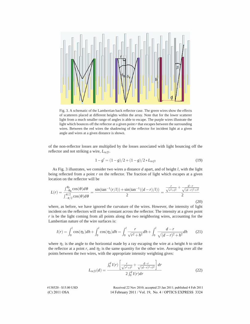
Fig. 3. A schematic of the Lambertian back reflector case. The green wires show the effectsof scatterers placed at different heights within the array. Note that for the lower scattererlight from a much smaller range of angles is able to escape. The purple wires illustrate thelight which bounces off the reflector at a given point r that escapes between the surroundingwires. Between the red wires the shadowing of the reflector for incident light at a givenangle and wires at a given distance is shown.
of the non-reflector losses are multiplied by the losses associated with light bouncing off thereflector and not striking a wire, Lre f l .
1−g′ = (1−g)/2+(1−g)/2∗Lre f l (19)
As Fig. 3 illustrates, we consider two wires a distance d apart, and of height l, with the lightbeing reflected from a point r on the reflector. The fraction of light which escapes at a givenlocation on the reflector will be
L(r) =
∫ θT−θB
cos(θ)dθ∫ π/2−π/2 cos(θ)dθ
=sin(tan−1(r/l))+ sin(tan−1((d− r)/l))
2=
r√r2+l2
+ d−r√(d−r)2+l2
2
(20)where, as before, we have ignored the curvature of the wires. However, the intensity of lightincident on the reflectors will not be constant across the reflector. The intensity at a given pointr is be the light coming from all points along the two neighboring wires, accounting for theLambertian nature of the wire surfaces is:
I(r) =∫ l
0cos(η1)dh+
∫ l
0cos(η2)dh =
∫ l
0
r√r2 +h2
dh+∫ l
0
d− r√(d− r)2 +h2
dh (21)
where η1 is the angle to the horizontal made by a ray escaping the wire at a height h to strikethe reflector at a point r, and η2 is the same quantity for the other wire. Averaging over all thepoints between the two wires, with the appropriate intensity weighting gives:
Lre f l(d) =
∫ d0 I(r)
[r√
r2+l2+ d−r√
(d−r)2+l2
]
dr
2∫ d
0 I(r)dr(22)
#138520 - $15.00 USD Received 22 Nov 2010; accepted 25 Jan 2011; published 4 Feb 2011(C) 2011 OSA 14 February 2011 / Vol. 19, No. 4 / OPTICS EXPRESS 3324
Lre f l(d) is inserted into Eq. (19) to find g′(d). We then take a weighted average of g′(d) withrespect to the angle subtended at each distance to find g′.
To find T ′int we note that light which impinges without striking the back reflector has a trans-
mission factor which remains unchanged from the non-reflector case. Thus, once the transmis-sion factor for light which bounces off the back reflector is calculated, these two transmissionfactors can be appropriately weighted together to give an overall transmission factor.
The approach to finding the transmission factor for light that has bounced off the back reflec-tor is similar the the approach for finding the transmission factor for incident side light. Thus,we take T0(β ) (see Eq. (11)), and weight it by the cosine dependence associated with the backreflector. Finally, we average over the position along the reflector with a weighting to accountfor the varying intensity, as shown below.
Tre f l(d)=
∫ d0 I(r)
(∫ π/2θT
∫ π/2−π/2 Tn cos(θ)cos2(φ)dαdθ +
∫ π/2θB
∫ π/2−π/2 Tn cos(θ)cos2(φ)dαdθ
)dr
∫ d0 I(r)
(∫ π/2θT
∫ π/2−π/2 cos(φ)cos(θ)dαdθ +
∫ π/2θB
∫ π/2−π/2 cos(φ)cos(θ)dαdθ
)dr
(23)Since, g′ − g is the additional light impingement which results from light which has struck
the back reflector, we find:
T ′int(d) =
g(d)Tint(d)+(g′(d)−g(d))Tre f l(d)
g′(24)
Then, the overall T ′int is a weighted average with the in-plane angles subtended at each distance.
Finally, g′ and T ′int are used in place of their unprimed counterparts in the multiple scattering
model (see Eq. (9)) to find L̄′.To find F̄ ′ we insert g′ and T ′
int in the multiple scattering model in place of their unprimedcounterparts. However, as Eq. (14) shows, we also need to find T ′
1 and g′1 To find g′1 we estimatethe impact of the reflector, R, using the following expression:
R = (1−g1(d))− (1−g(d))/2 (25)
This estimates the amount of light that would be lost, but instead strikes the reflector. Becausethe top part will always be shadowed last, we assume the losses from the top are constant andequal (1−g(d))/2. Thus, everything else will strike the reflector, and we use our previous resultfor Lre f l to find the total losses, 1−g′1(d).
1−g′1(d) = R∗Lre f l +(1−g(d))/2 (26)
This allows us to modify the transmission factor:
T ′1(d) =
T1(d)g1(d)+Tre f l(d)(g′1(d)−g1(d))
g′1(d)(27)
Inserting all the primed quantities for their unprimed counterparts in the equation for F̄ , anddividing by two to account for the hemispherical illumination gives F̄ ′. Obviously, the shad-owing fraction, u, and the transmission factor prior to any reflection, T0, are unchanged by thepresence of the reflector since the sun is directly striking the wire.
To find R̄′, we first determine the shadowing of the reflector as a function of wire to wire
#138520 - $15.00 USD Received 22 Nov 2010; accepted 25 Jan 2011; published 4 Feb 2011(C) 2011 OSA 14 February 2011 / Vol. 19, No. 4 / OPTICS EXPRESS 3325
distance and angle of incidence. From Fig. 3, the shadowed fraction of the reflector u(d,β ) is:
u(d,β ) =d− l tan(β )
d(28)
Taking a weighted average with respect to angle subtended at a given distance gives u(β ), weaverage over all β ’s, including the differential solid angle and a weighting for intensity, to findu.
u =
∫ π/20 u(β )sin(β )cos(β )dβ∫ π/2
0 sin(β )cos(β )dβ(29)
Next we develop a multiple scattering model. The losses from light that doesn’t hit a wireafter the initial reflection is Linc, which we find by averaging L(r) over the unshadowed por-tion of the reflector at each distance, with appropriate weighting for shadowing and the anglesubtended at each distance. Tinc, the transmission of light after initial reflection, is found in anexactly analogous manner. (1− Linc)(1−Tinc) is reflected back into the array after bouncingonce off the wire. From the previous result, (1−g′)/(1−g′(1−T ′
int)) of this light will be lost.Thus, the total losses for light that initially strikes the reflector are:
Ltot = Linc +(1−Linc)(1−Tinc)1−g′
1−g′(1−T ′int)
(30)
Then,R̄′ = (1−Ltot)u (31)
To find R̄′, we have approximated the the shadowing of the reflector using the closest distancebetween two wires, leading to an overestimation of the shadowing impact, which should belarger for high filling fractions. This is consistent with our use of the closest distance betweentwo wires for wire to wire shadowing and and losses.
5. Results for wire array intensity enhancement with a Lambertian back reflector
Inserting the terms derived above into Eq. (18), we find the light trapping factor, which is plottedas a function of filling fraction in Fig. 2 by the curves labeled “Lambertian back reflector”.The results closely approach the relevant ergodic limit of 2n2 for large filling fractions as theterms involving the wire sides and the reflector become very small. As in the no back reflectorcase, the light trapping factor falls below the ergodic limit as the filling fraction is decreasedfrom the maximum. It seems likely that, as before, the overestimation of L̄ in the radial escapeapproximation for these filling fractions is at least partially responsible for the decrease. Thisis supported by the trend in aspect ratios, which is similar to that for the no back reflector case.
Interestingly, we see that for small filling fractions, the light trapping increases asymptoti-cally, significantly exceeding the ergodic limit, in contrast to the no back reflector case. As wepreviously noted, our approximations improve with decreasing filling fractions. Thus, there isno reason to suspect that surpassing the ergodic limit is an artifact of the modeling assumptions.Furthermore, we can understand the observed asymptotic increase physically by consideringthe limit of small filling fraction. For very small filling fractions the side loss factor, L̄′, andthe side transmission factor, F̄ ′, are nearly constant, as they have nearly reached their maxima.In addition, the radius is rapidly approaching zero. Thus, all the terms in Eq. (18), with theexception of the back reflector term, are decreasing as the square of the radius. However, thereflector area remains nearly constant with decreasing filling fraction, as the array is already al-most entirely reflector. Thus, if R̄′ is decreasing less quickly than the radius squared, we shouldsee asymptotic increase. In fact, fitting the asymptotic regions of each of the curves we find
#138520 - $15.00 USD Received 22 Nov 2010; accepted 25 Jan 2011; published 4 Feb 2011(C) 2011 OSA 14 February 2011 / Vol. 19, No. 4 / OPTICS EXPRESS 3326
that the curves are increasing as r−p, where p has values between 0.33 and 0.37. Figure 4 usesthe fit in the calculation of the power, to give a sense of the goodness of the fit. The fits arequite good across all the curves, and the values of p do not trend with aspect ratio. These fitssuggests that the back reflector transmission goes approximately as the radius to the 5/3 powerin the low filling fraction regime, across the range of aspect ratios explored here. The variationof the onset of asymptotic behavior with aspect ratio is also consistent with this explanation, asthe denominator of the light trapping factor will decrease more rapidly for shorter wires.
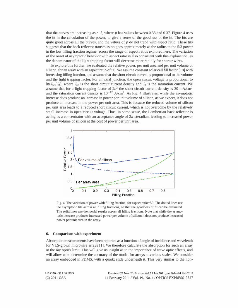
To explore this further, we evaluated the relative power, per unit area and per unit volume ofsilicon, for an array with an aspect ratio of 50. We assume constant solar cell fill factor [18] withincreasing filling fraction, and assume that the short circuit current is proportional to the volumeand the light trapping factor. For an axial junction, the open circuit voltage is proportional toln(Jsc/J0), where Jsc is the short circuit current density and J0 is the saturation current. Weassume that for a light trapping factor of 2n2 the short circuit current density is 30 mA/cm2
and the saturation current density is 10−12 A/cm2. As Fig. 4 illustrates, while the asymptoticincrease does produce an increase in power per unit volume of silicon, as we expect, it does notproduce an increase in the power per unit area. This is because the reduced volume of siliconper unit area leads to a reduced short circuit current, which is not overcome by the relativelysmall increase in open circuit voltage. Thus, in some sense, the Lambertian back reflector isacting as a concentrator with an acceptance angle of 2π steradian, leading to increased powerper unit volume of silicon at the cost of power per unit area.
Fig. 4. The variation of power with filling fraction, for aspect ratio=50. The dotted lines usethe asymptotic fits across all filling fractions, so that the goodness of fit can be evaluated.The solid lines use the model results across all filling fractions. Note that while the asymp-totic increase produces increased power per volume of silicon it does not produce increasedpower per unit area in the array.
6. Comparison with experiment
Absorption measurements have been reported as a function of angle of incidence and wavelenthfor VLS-grown microwire arrays [1]. We therefore calculate the absorption for such an arrayin the ray optics limit. This will give us insight as to the importance of wave optic effects, andwill allow us to determine the accuracy of the model for arrays at various scales. We consideran array embedded in PDMS, with a quartz slide underneath it. This very similar to the non-
#138520 - $15.00 USD Received 22 Nov 2010; accepted 25 Jan 2011; published 4 Feb 2011(C) 2011 OSA 14 February 2011 / Vol. 19, No. 4 / OPTICS EXPRESS 3327

reflector case, except for the fact that we have PDMS/quartz (n=1.4) instead of free space. Inaddition, we include an absorption term in the governing equation. As Yablonovitch has shown,this term should be equal to 2αVIint where α is the absorption coefficient, and V is the volumewhere the absorption is occurring [14].
Thus, the governing equation for a given angle of incidence θ , is:
A′sidesImax sin(θ)F(θ)+2AendImax cos(θ)T (θ) = 2αVIint +
2AendT̄endIint
n2 +AsidesL̄Iint
n2 (32)
where Imax is the intensity of the incident light at normal incidence, and the factors of sin(θ)and cos(θ), account for the decreased intensity at non-normal incidence. Note that for the lightentering through the sides we have A′
sides instead a Asides, to denote that we need to accountfor decreased intensity as the wire turns away from the in-plane direction from which the lightenters. Rearranging to find Iint gives:
Iint =A′
sidesImax sin(θ)F(θ)+2AendImax cos(θ)T (θ)
2αV + 2Aend T̄endn2 + AsidesL̄
n2
(33)
The fraction of light absorbed, A, is:
A =2αVIint
Atot Imax cos(θ)=
2αV (A′sidesF(θ) tan(θ)+2AendT (θ))
Atot(2αV + 2Aend T̄endn2 + AsidesL̄
n2 )(34)
where Atot is the total area of one unit cell. With the exception of A′sides, these terms follow
directly from our previous work. However, between various in plane angles, the amount ofshadowing will vary. Previously, to find F̄ we averaged this over all the in-plane angles. Ex-perimentally, though, the light will only come from one in-plane direction, which, in this case,was aligned in the direction of maximal shadowing. In addition, to account for a non-free spacemedium, all the factors of 1/n2 are replaced with n2
1/n22, where n1 is the index of the embedding
medium and n2 is the index of the wires, due to the relative density of modes between the twomedia.
To find the experimental absorption data, arrays of silicon microwires were grown by theVLS mechanism from SiCl4 precursors as reported previously [19]. The geometry of the arrayswas defined by the photolithographic mask used to pattern the VLS catalyst islands. Wires witha radius of 1μm were grown from a hexagonally packed mask with 3 μm diameter holes witha center to center spacing of 9 μm. Larger wires with a radius of approximately 4 μm weregrown from a hexagonally packed mask with 15 μm diameter holes and 30 μm center to centerspacing.
After growth, the metal VLS catalyst was removed from the wires and the height and diame-ter of the wires were measured using scanning electron microscopy. The wires were embeddedin polydimethylsiloxane (PDMS, Sylgard) as reported previously [19]. The PDMS was drop-cast onto the wires and spun at 3000 rpm, and then cured at 120 ◦C for 30 minutes. Wireswere removed from the substrate by scraping the PDMS film with a razor blade. Integratedreflection and transmission measurements were performed with a custom- built 4 inch integrat-ing sphere apparatus using a Fianium supercontinuum laser illumination source and a 0.25 mmonochromator [1]. The absorption of each sample was determined from the wavelength andangle resolved transmission and reflection measurements [6].
We then input structural parameters, as determined by SEM, from these measured arraysinto the model developed above. The PDMS embedding material was included in the model,but the PDMS/air interface was neglected. (The PDMS/air interface gives about 3% reflection).
#138520 - $15.00 USD Received 22 Nov 2010; accepted 25 Jan 2011; published 4 Feb 2011(C) 2011 OSA 14 February 2011 / Vol. 19, No. 4 / OPTICS EXPRESS 3328
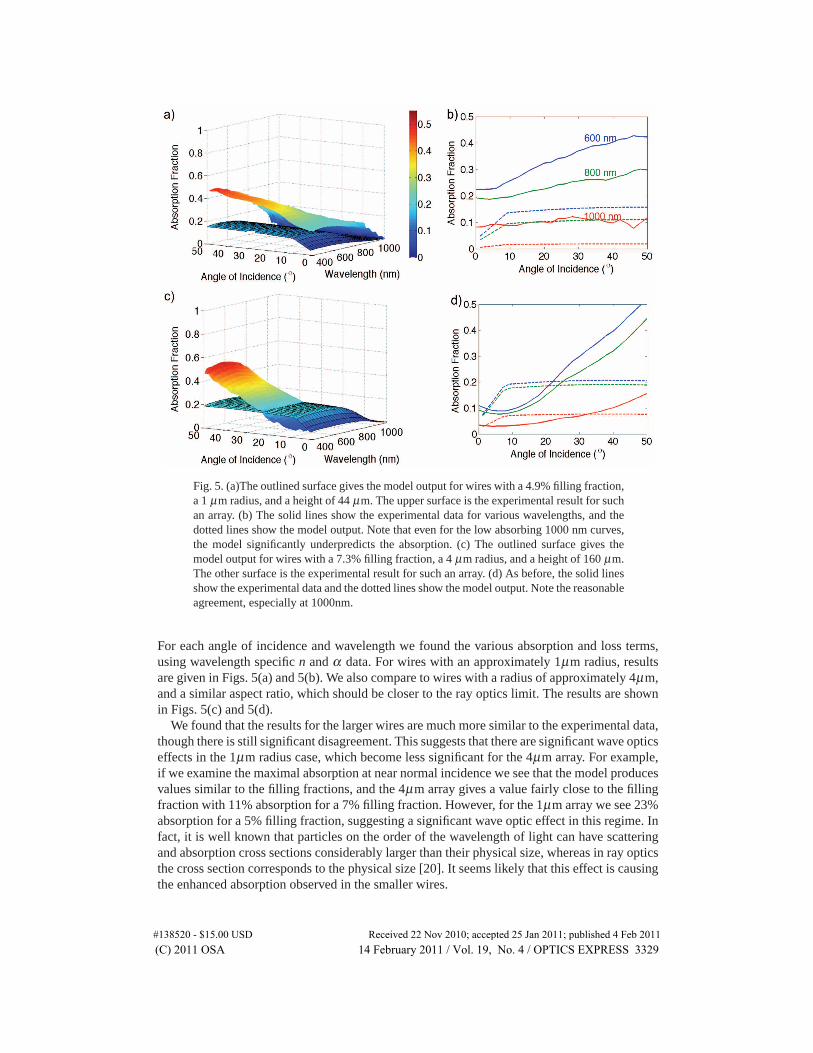
Fig. 5. (a)The outlined surface gives the model output for wires with a 4.9% filling fraction,a 1 μm radius, and a height of 44 μm. The upper surface is the experimental result for suchan array. (b) The solid lines show the experimental data for various wavelengths, and thedotted lines show the model output. Note that even for the low absorbing 1000 nm curves,the model significantly underpredicts the absorption. (c) The outlined surface gives themodel output for wires with a 7.3% filling fraction, a 4 μm radius, and a height of 160 μm.The other surface is the experimental result for such an array. (d) As before, the solid linesshow the experimental data and the dotted lines show the model output. Note the reasonableagreement, especially at 1000nm.
For each angle of incidence and wavelength we found the various absorption and loss terms,using wavelength specific n and α data. For wires with an approximately 1μm radius, resultsare given in Figs. 5(a) and 5(b). We also compare to wires with a radius of approximately 4μm,and a similar aspect ratio, which should be closer to the ray optics limit. The results are shownin Figs. 5(c) and 5(d).
We found that the results for the larger wires are much more similar to the experimental data,though there is still significant disagreement. This suggests that there are significant wave opticseffects in the 1μm radius case, which become less significant for the 4μm array. For example,if we examine the maximal absorption at near normal incidence we see that the model producesvalues similar to the filling fractions, and the 4μm array gives a value fairly close to the fillingfraction with 11% absorption for a 7% filling fraction. However, for the 1μm array we see 23%absorption for a 5% filling fraction, suggesting a significant wave optic effect in this regime. Infact, it is well known that particles on the order of the wavelength of light can have scatteringand absorption cross sections considerably larger than their physical size, whereas in ray opticsthe cross section corresponds to the physical size [20]. It seems likely that this effect is causingthe enhanced absorption observed in the smaller wires.
#138520 - $15.00 USD Received 22 Nov 2010; accepted 25 Jan 2011; published 4 Feb 2011(C) 2011 OSA 14 February 2011 / Vol. 19, No. 4 / OPTICS EXPRESS 3329

Despite the reasonable agreement for angles of incidence relatively near normal, the rayoptics model fails to capture the strong increase in absorption observed with large angles ofincidence for wavelengths where the absorption is strong. However, our model assumes that thelight is fully randomized before any significant absorption takes place, which will not occur instrongly absorbing wavelength regimes. Thus, it is not surprising that our model fails to explainthis behavior. As we expect, the agreement is improved for wavelengths where the absorption islow and this randomization condition is more accurate, as is shown in Fig. 5(d). However, evenin this case, the shape of the curve is not captured particularly accurately, most likely due todifferences between the experimental and modeled wires. For example, if the experimental wiresurfaces were not perfectly Lambertian, but somewhat specular, the angular profile would likelybe sloped across a wider range of angles, as is seen here. This is because the light which strikesthe wire sides would reflect in one direction rather than be scattered in all directions, so light atnear normal incidence would be less likely to enter the sides than for specular wires. Thus, ourmodel works reasonably well in the low absorbing ray optics regime, but does not quite capturethe angular dependence, perhaps due to non-Lambertian experimental wire surfaces.
7. Conclusion
The model developed in this paper addresses wire geometries from a ray optics perspective,assuming Lambertian surfaces and weak absorption. In the non-reflector case, the model pro-duces light trapping close to the ergodic limit of n2 for filling fractions approaching zero andapproaching unity. This conforms with our thermodynamic expectation and allows us to un-derstand the accuracy of the approximations used for computational feasibility. In addition,it confirms our physical expectations about the regimes for which the approximations will bemost accurate.
Applying the model to the case of a Lambertian back reflector, we observe significant inten-sity enhancements, including asymptotic increases for small filling fractions that significantlyexceed the ergodic limit of 2n2. Quantitatively, for a filling fraction of 0.1%, the enhancementcan exceed 3n2, and the asymptotic increase goes approximately as r−1/3, where r is the wireradius. These asymptotic increases result from the reflector acting as a concentrator with anacceptance angle of 2π steradian, and fitting them gives insight into the asymptotic behavior ofthe transmission factor for light that initially strikes the reflector, which goes as approximatelyr5/3. It seems that a more sophisticated back reflector, which preferentially scattered sideways,could allow for asymptotic behavior which would be even more dramatic, a topic that deservesfurther study. However, while the asymptotic increases found here do give increased power pervolume of silicon, there is reduced power per unit wire array area, owing to reduced siliconvolume at low filling fractions.
Finally, in comparing the model with experimental absorption data, there is agreement withexperiment for large (4 μm radius) wires in the low absorbing regime where the model is valid.The results suggest that the very strong absorption observed in smaller wires (1 μm radius)may be significantly due to wave optical effects, and analysis using a wave optics formalismis required in order to understand this strong absorption. Thus, even though previous modelinghas suggested large wires could be superior from a device physics perspective, they appear tobe less optimal from a light trapping perspective. This trade-off deserves further study, as dothe wave optics effects observed in smaller wires.
Acknowledgements
The authors thank M. Kelzenberg for provision of data and insightful discussion, D. Callahanfor advice on the manuscript and E. Warmann for assistance with figures. This material is basedupon work supported as part of the Light Matter Interaction in Energy Conversion, an Energy
#138520 - $15.00 USD Received 22 Nov 2010; accepted 25 Jan 2011; published 4 Feb 2011(C) 2011 OSA 14 February 2011 / Vol. 19, No. 4 / OPTICS EXPRESS 3330

Frontier Research Center funded by the U. S. Department of Energy, Office of Science, Officeof Basic Energy Sciences under Award Number DE-SC0001293.
#138520 - $15.00 USD Received 22 Nov 2010; accepted 25 Jan 2011; published 4 Feb 2011(C) 2011 OSA 14 February 2011 / Vol. 19, No. 4 / OPTICS EXPRESS 3331