Insights in the light trapping effect in silicon solar ...
14
Insights in the light trapping effect in silicon solar cells with backside diffraction gratings Markus Wellenzohn Rainer Hainberger Downloaded From: https://www.spiedigitallibrary.org/journals/Journal-of-Photonics-for-Energy on 25 Nov 2021 Terms of Use: https://www.spiedigitallibrary.org/terms-of-use
Transcript of Insights in the light trapping effect in silicon solar ...

Insights in the light trapping effect insilicon solar cells with backsidediffraction gratings
Markus WellenzohnRainer Hainberger
Downloaded From: https://www.spiedigitallibrary.org/journals/Journal-of-Photonics-for-Energy on 25 Nov 2021Terms of Use: https://www.spiedigitallibrary.org/terms-of-use

Insights in the light trapping effect in siliconsolar cells with backside diffraction gratings
Markus Wellenzohn and Rainer HainbergerAIT Austrian Institute of Technology GmbH, Health & Environment Department,
Vienna 1220, [email protected]
Abstract. Light trapping by means of backside diffraction gratings can strongly increase the effi-ciency in silicon solar cells. However, the optimization of the grating geometry involves compre-hensive multiparameter scans, which necessitates an efficient simulation method. In this study, weemploy a simulation approach that combines ray tracing with rigorous coupled wave analysis. Asan additional benefit, this approach provides a much better physical insight into the light trappingmechanism in contrast to fully electromagnetic simulation methods. The influence of the ray trac-ing simulation settings in terms of recursion depth and diffraction order on the simulation results isinvestigated. We show that the choice of a proper recursion depth and a sufficient number of dif-fraction orders is essential for obtaining fully optimized grating parameters and that the minimumrecursion depth required for obtaining the correct optimized grating parameters depends on thesilicon thickness. Furthermore, we investigate the influence of the angle of incidence on the opti-mized grating parameters. As major result, we find that the optimum grating structure does notdepend on the angle of incidence on the solar cell. © The Authors. Published by SPIE under a CreativeCommons Attribution 3.0 Unported License. Distribution or reproduction of this work in whole or in partrequires full attribution of the original publication, including its DOI. [DOI: 10.1117/1.JPE.3.034595]
Keywords: light trapping; diffraction grating; nanostructures; silicon solar cells; simulation;rigorous coupled wave analysis.
Paper 13014 received Jun. 7, 2013; revised manuscript received Aug. 20, 2013; accepted forpublication Aug. 23, 2013; published online Sep. 26, 2013.
1 Introduction
The efficiency enhancement of silicon solar cells by increasing the interaction length of light atweakly absorbed wavelengths using backside diffraction gratings has been widely studied.1–10
However, several aspects that require systematic in-depth analysis have not been sufficientlyaddressed so far. We have recently introduced a simulation procedure11–13 combining a two-dimensional ray tracing algorithm with rigorous coupled wave analysis (RCWA) that facilitatescomprehensive studies on the efficiency enhancement in silicon solar cells by means of backsidediffraction gratings. Compared to the fully electromagnetic simulation methods, RCWA andfinite difference time domain (FDTD), the major benefit of this combined approach is thestrongly reduced computation time and the gain in simulation precision, in particular forcells with an absorber thicker than 10 μm. Previously, we have already applied this combinedRCWA/ray tracing approach to study the influence of the absorber thickness on the optimumgrating parameters providing maximum photocurrent densities.11 In this article, we present an in-depth analysis of the influence of simulation parameters, such as the recursion depth or the dif-fraction order and the number of diffraction orders on the simulation outcomes. This analysis notonly reveals the requirements for achieving a correct optimization of the grating parameters butalso provides unprecedentedly a clear picture of the light trapping mechanism. Furthermore, forthe first time to the best of our knowledge, we investigate the influence of the angle of incidenceof sunlight on the optimum parameters of backside gratings.
2 Simulation Method and Coherence of Sunlight
Figure 1 shows the silicon solar cell model with a backside diffraction grating investigated in thisarticle and a reference structure without grating. In this article, we exclusively use a duty cycle of
Journal of Photonics for Energy 034595-1 Vol. 3, 2013
Downloaded From: https://www.spiedigitallibrary.org/journals/Journal-of-Photonics-for-Energy on 25 Nov 2021Terms of Use: https://www.spiedigitallibrary.org/terms-of-use

the diffraction gratings which is 1:1. The flat front surface is covered with a single layer anti-reflection (AR) coating made of 80-nm silicon nitride (SiNx). The backside is covered with a100-nm-thin SiO2 layer and an aluminum electrode. The SiO2 layer improves the reflectance ofthe backside aluminum electrode.
In our approach, the front side thin film AR coating and the backside diffraction gratingincluding a thin film SiO2 coating are treated in a fully coherent way, whereas the siliconlayer is treated incoherently. In a first step, the reflectivity and transmissivity of the frontside AR coating were calculated as polarization dependent functions of the angle of incidenceand employing the standard equations for a homogeneous dielectric film.14 Furthermore, thediffraction efficiencies of the backside gratings were also determined for different period lengthsand modulation depths depending on the angle of incidence, wavelength, polarization, and dif-fraction order m by means of RCWA. All these resulting data were interpolated to accelerate thecomputation in the subsequent ray tracing, in which the overall light absorption inside the siliconwas calculated. In this ray tracing algorithm, light rays with different wavelengths entering thesilicon layer are traced for a certain number of zig-zag reflections inside the silicon layer. Therecursion depth counts the number of reflections at the backside grating of each light ray,taken into account for calculating the absorption. In our simulations, each ray is traced insidethe silicon layer until either its fractional intensity is smaller than a minimum limit(Iray∕Iin < 10−5) or the number of reflections/diffractions at the backside grating exceededthe recursion depth r. The ray tracing is performed for different wavelengths and for both polar-izations. As the light rays propagate inside the silicon layer the wavelength dependent absorptionis summed up according to Beer–Lambert’s law.11 Finally, the absorption was integrated over thewavelength range 300 to 1140 nm, and averaged over both polarizations. The photocurrent den-sity is defined by
Jph ¼ eZ
λ¼1140 nm
λ¼300 nm
AðλÞSðλÞdλ; (1)
where AðλÞ is the photon absorption inside the silicon, SðλÞ is the incident photon flux, and e isthe elementary charge.11 In this article, the photocurrent density was calculated by summing upthe number of absorbed photons over the solar spectrum air mass coefficent (AM 1.5). over bothpolarizations. It was assumed that each absorbed photon generates an electron hole pair withoutconsidering electrical losses.
Green’s complex refractive index data for silicon are used,15 and for the complex refractiveindex data of Al and SiO2 were used.
16–18 Further details on this combined RCWA/ray tracingapproach can be found in Refs. 11–13 and 19.
This combined coherent/incoherent approach can be justified in the following way. Thecoherence length of sunlight measured by means of a Michelson interferometer has been esti-mated to be about 600 nm, under the assumption that the sun is a black body radiator emittingphotons at temperature of T ∼ 6000 K.20 It is often argued that for optical path lengths longerthan this coherence length no interference occurs and, therefore, an incoherent treatment isappropriate. From this point of view the incoherent treatment of silicon layers with a thicknessof ≥1 μm would be well justified. However, in fact etalons of several microns thickness still actas thin film filters which are well known to increase the coherence length.21 Therefore, it can be
Fig. 1 Investigated silicon solar cell models (a) with and (b) without backside diffraction grating(reference cell).
Wellenzohn and Hainberger: Insights in the light trapping effect in silicon solar cells. . .
Journal of Photonics for Energy 034595-2 Vol. 3, 2013
Downloaded From: https://www.spiedigitallibrary.org/journals/Journal-of-Photonics-for-Energy on 25 Nov 2021Terms of Use: https://www.spiedigitallibrary.org/terms-of-use

expected that Fabry–Perot resonances also occur for silicon layers of several microns thickness.In this partially coherent regime, the fringe visibility of the Fabry–Perot resonances will decreasewith increasing layer thickness. Moreover, the spectral distance between two resonancesdecreases with increasing silicon layer thickness. In terms of absorption and, thus, photocurrent,the effect of these Fabry–Perot resonances is negligible, and an incoherent treatment of the sil-icon layer is acceptable.
In order to validate the combined RCWA/ray tracing approach, we compared the simulationoutcomes of the photocurrent densities with the results obtained by a full RCWA simulation forthin cells. Figure 2 plots the absorption spectra calculated by the combined RCWA/ray tracingapproach and the absorption spectra obtained from fully coherent RCWA simulations for thincells with thicknesses of 1, 3, and 10 μm as well as the spectra for the corresponding referencecells without grating (dashed curves). For both methods, the results of the two polarizations[transverse electric (TE) and transverse magnetic (TM)] were averaged. In the combinedRCWA/ray tracing approach, a recursion depth of r ¼ 8 was chosen and the highest orderof diffraction taken into account was set to m ¼ �5.
The absorption spectra calculated with full RCWA (blue curves in Fig. 2) show oscillationscaused by interference effects inside the silicon while for the spectra calculated with the com-bined RCWA/ray tracing approach these interference effects are taken into account. In particularfor thin cells, strong oscillations due to interference effects occur under the assumption of acoherent light. These oscillations are largely averaged out in the calculation of the photocurrentdensities. The deviations of the photocurrent densities between the two methods amount to about4% for dSi ¼ 1 μm, 1.7% for dSi ¼ 3 μm, and 0.9% for dSi ¼ 10 μm. Thus, with increasingsilicon thickness the differences get smaller because interference effects play a less importantrole.
A significant advantage of the combined simulation method is that the RCWA-based calcu-lation of the backside grating diffraction efficiency can be performed for a thin simulationdomain without including the absorber layer. This allows the use of a sufficiently large numberof harmonics, in this article 35, guaranteeing a high precision of the simulation outcomes in-dependent of the silicon absorber thickness. By contrast, the precision of full RCWA simulationsof the whole solar cell structure including the absorber layer will drop rapidly for thicknessesexceeding a few microns, because the number of harmonics has to be reduced due to limitationsin computer memory and computation time. Therefore, especially for cells with a thickness dSi >10 μm the combined RCWA/ray tracing simulation approach is highly favourable compared tofull electromagnetic simulation methods, such as RCWA and FDTD because, the simulationscan be performed with a sufficiently large number of harmonics.
As an additional benefit, the incoherent treatment of the silicon absorption layer provides amuch better physical insight into the light trapping mechanism, which cannot be gainedwhen using fully coherent simulation methods, where Fabry–Perot resonances obscure thecharacteristic humps in the absorption spectra (see Fig. 2) which will be described in detailin Sec. 3.
Fig. 2 Absorption spectra calculated by the combined rigorous coupled wave analysis (RCWA)/ray tracing approach and by full RCWA simulations averaged for TE and TM polarization for thinsilicon solar cells with a thickness of 1, 3, and 10 μm. The dashed red lines indicate the results ofthe combined RCWA/ray tracing approach for cells without backside grating (w.g.). The symbol #indicates the number of harmonics used for the RCWA simulations.
Wellenzohn and Hainberger: Insights in the light trapping effect in silicon solar cells. . .
Journal of Photonics for Energy 034595-3 Vol. 3, 2013
Downloaded From: https://www.spiedigitallibrary.org/journals/Journal-of-Photonics-for-Energy on 25 Nov 2021Terms of Use: https://www.spiedigitallibrary.org/terms-of-use

3 Light Trapping Mechanism in Silicon Solar Cells with BacksideDiffraction Gratings
Light trapping by means of backside diffraction gratings relies on the deflection of incident lightto propagation angles above the critical angle of total internal reflection (ΘTIR). This can con-siderably enhance the interaction length and, thus, the absorption of light within the silicon layer.The diffraction angles inside the silicon layer of the solar cell can be calculated by
Θmðλ;ΛÞ ¼ arcsin
�sinðΘinÞnsiðλÞ
þ mλ
nsiðλÞΛ�; (2)
where λ is the wavelength, Θin is the angle of incidence on the solar cell front side in air,m is thediffraction order, Λ is the grating period, and nSiðλÞ is the refractive index of silicon.22 In addi-tion, the following inequality has to be fulfilled
���� sinðΘinÞ þmλ
Λ
���� ≤ nsiðλÞ; (3)
which means that for a given grating period and diffraction order there is an upper wavelengthlimit above which no diffraction can occur.22
Figure 3(a) plots the wavelength dependent angles of first-order diffraction (m ¼ 1) for dif-ferent grating periods (400 to 1000 nm) in the case of normal incident light calculated by Eq. (1).From this equation, it follows that for normal incident light (Θin ¼ 0) the diffraction angle equalsthe angle of TIR, ΘTIR ¼ arcsinð1∕nSiÞ, if λ ¼ Λ. Two regions can be distinguished: in region I(λ < Λ), the diffraction angles are smaller than the ΘTIR and, thus, lie within the escape cone [seeFig. 1(a)], where no significant light trapping can occur; in region II (λ > Λ), the diffractionangles are larger than ΘTIR and, therefore, all rays are totally reflected at the front surfaceback into the silicon for further absorption. According to Eq. (2) for higher diffraction ordersthe angle of diffraction exceeds ΘTIR at much shorter wavelengths. For example, in Fig. 3(a) theline representing the diffraction angles for the case Λ ¼ 500 nm and m ¼ 1 corresponds to thecase Λ ¼ 1000 nm and m ¼ 2.
Figure 3(b) shows the calculated absorption spectra of silicon solar cells with backside gra-tings optimized for different thicknesses ranging from 1 to 200 μm in the case of normal incidentlight.11 The results were obtained for a recursion depth of r ¼ 5, which provided the best com-promise between accuracy and computation time. The highest order of diffraction taken intoaccount was set to 5. Further details on the influence of these parameters will be given inSecs. 4 and 5.
The absorption spectra in Fig. 3(b) provide additional insight into the light trapping effect.Significant absorption humps occur in distinctive wavelength regions which are related to theoptimized grating periods. At wavelengths similar to the respective optimized grating period, the
Fig. 3 (a) First-order diffraction angles Θþ1ðλ;ΛÞ and angle of TIR at the Si/SiNx/air interface (redcurve); (b) calculated absorption spectra averaged over TE and TM polarization in silicon solarcells with planar backside electrode (dashed lines) and with optimized backside gratings for siliconthicknesses ranging from 1 to 200 μm. For 1 μm thickness the absorption spectra of TE and TMpolarization are also plotted separately.
Wellenzohn and Hainberger: Insights in the light trapping effect in silicon solar cells. . .
Journal of Photonics for Energy 034595-4 Vol. 3, 2013
Downloaded From: https://www.spiedigitallibrary.org/journals/Journal-of-Photonics-for-Energy on 25 Nov 2021Terms of Use: https://www.spiedigitallibrary.org/terms-of-use

absorption significantly rises. At higher wavelengths, the humps have a falling slope where theenhancement drops abruptly but the absorption still remains at values higher than that of solarcells without grating indicated by dashed lines. In the following, the light trapping mechanismand the origin of the humps will be analyzed in more detail for solar cells with thicknesses of1 μm. As can be seen from Fig. 3(b), the shapes of the absorption spectra for TE and TM polari-zation show very similar behavior because the underlying diffraction mechanism is the same. Wetherefore restrict this analysis to TE polarization without loss of generality. Figure 4(d) plots thespectral diffraction efficiencies of normal incident TE polarized light for the optimized gratingstructure (Λ ¼ 625 nm, h ¼ 50 nm) and m ¼ 0; : : : ;þ5. For reasons of symmetry, the diffrac-tion efficiencies of the negative orders (m ¼ −1; : : : ;−5) are the same for Θin ¼ 0 deg. In thespectral region with wavelengths slightly larger than the optimized grating periods, the zero-order diffraction efficiencies strongly decrease, while the first-order diffraction efficienciesrise sharply. The rising slope of the hump is caused by the increasing first-order diffractionangle [see Fig. 3(a)], which translates into a higher reflectivity at the upper interface with increas-ing wavelength peaking at λ ¼ Λ, where TIR occurs. Light with λ ≥ Λ is totally internallyreflected back into the silicon resulting in a longer interaction length and, therefore, largerabsorption.
The abruptly falling slopes of the humps in the absorption spectra of Fig. 3(b) can beexplained by the limit of diffraction given by Eq. (2), where the diffraction angle for a certaindiffraction order approaches 90 deg. Above this cut-off wavelength no diffraction can occur. Theinteraction length of rays diffracted to large angles increases dramatically, thus resulting in astrong contribution even though the diffraction efficiency might be comparatively low. This
Fig. 4 (a), (b), and (c) Calculated absorption spectra of TE polarized light in a 1-μm-thin siliconsolar cell with optimized diffraction grating (Λ ¼ 625 nm, h ¼ 50 nm) for recursion depth r ¼ 1, 2,and 3 taking into account different numbers of diffraction ordersm ≤ mmax; (d), (e), and (f) spectraldiffraction efficiencies of different diffraction orders for angles of incidence Θin;0 ¼ 0 deg, Θin;1ðλÞ,and Θin;2ðλÞ.
Wellenzohn and Hainberger: Insights in the light trapping effect in silicon solar cells. . .
Journal of Photonics for Energy 034595-5 Vol. 3, 2013
Downloaded From: https://www.spiedigitallibrary.org/journals/Journal-of-Photonics-for-Energy on 25 Nov 2021Terms of Use: https://www.spiedigitallibrary.org/terms-of-use

fact is illustrated by Fig. 5(a), which plots the diffraction angles on a grating with Λ ¼ 625 nm asa function of wavelength for the discrete angle of incidences. Figure 5(a) clearly shows that forhigher diffraction orders, which are indicated by the subscript index, the corresponding diffrac-tion angles given by Eq. (2) reach the limit of diffraction at much smaller wavelengths comparedto lower diffraction orders. For comparison the angle of TIR is also inserted in Fig. 5(a) (redcolored line). Figure 5(b) shows the enhancement of the single round trip (SRT) interactionlength for photons with diffraction angles Θout;mðλÞ (m ¼ �1; : : : ;�5) larger than the ΘTIR.The enhancement of the SRT interaction length is given by the ratio between the opticalpath length from the point of diffraction at the grating to the next incidence on the gratingand 2dSi, which represents the SRT interaction length for normal incidence in a solar cellwith a planar backside. This enhancement amounts to 1∕cosΘout;mðλÞ.
In the following, we discuss the origin of the falling slope of the hump in the absorptionspectrum in more detail for the diffraction grating with a period of Λ ¼ 625 nm and a modu-lation depth of h ¼ 50 nm. For this grating the abruptly falling slope occurs near the wavelengthof 780 nm. In Figs. 4(a)–4(c) the associated absorption spectra are plotted for different recursiondepths r and maximum diffraction orders mmax taken into account. Figures 4(d)–4(f) plot theefficiencies of different diffraction orders for three distinctive angles of incidences on the gratingΘin;0 ¼ 0 deg, Θin;1ðλÞ, and Θin;2ðλÞ, respectively. The angles of incidences Θin;1ðλÞ and Θin;2ðλÞoccur if normal incident photons are diffracted into the first (m ¼ 1) or second diffraction order(m ¼ 2), respectively, get reflected at the front side, and again hit the grating. One finds that forthe recursion depth r ¼ 1 the falling slope appears if diffraction up to the third-order is taken intoaccount (mmax ¼ 3). For the recursion depth r ¼ 2, the falling slope becomes observable if dif-fraction up to the second-order is considered (mmax ¼ 2). Accordingly, for recursion depth r ¼ 3
the falling slope can be found already if only first-order diffraction (mmax ¼ 1) is taken intoaccount. This behavior can be explained by the fact that in all three cases the diffraction effi-ciencies of the corresponding highest considered diffraction orders become zero for wavelengthsλ > 780 nm, i.e., where Θout becomes 90 deg. The diffraction angle Θout ¼ 90 deg can bereached for normal incident light (Θin;0 ¼ 0 deg) by third-order diffraction (m ¼ 3), or forlight incident with Θin;1 by second-order diffraction (m ¼ 2), or for light incident with Θin;2
by first-order diffraction (m ¼ 1). The first case can occur already for a recursion depthr ¼ 1 with mmax ≥ 3, whereas the second case requires a diffraction into Θin;1, which onlycan occur for recursion depth r ≥ 2. If the order of diffractions taken into account is limitedto jmj ≤ 1, the third case can only occur for at least three interactions of the ray with the grating,i.e., r ≥ 3.
As can be seen in Fig. 3(b), the humps in the absorption spectra of thin solar cells withoptimized backside gratings occur at much shorter wavelengths than that of thicker cells.The reason for this behavior is given by the fact that in thin cells even short wavelength photons,which have a stronger contribution to the solar spectrum, can reach the backside diffractiongrating before getting absorbed inside the silicon layer. The comparison of the absorption spectrain Fig. 3(b) clearly shows that the light trapping effect is most pronounced for thin solar cells.
(a) (b)
Fig. 5 (a) Diffraction angle spectrum in a silicon solar cell with a backside grating of periodΛ ¼ 625 nm. (b) Optical path length enhancement of normally incident light for SRT from thefirst to the second diffraction at the backside grating in multiples of the path length 2dSi
(m ¼ 1; : : : ; 5).
Wellenzohn and Hainberger: Insights in the light trapping effect in silicon solar cells. . .
Journal of Photonics for Energy 034595-6 Vol. 3, 2013
Downloaded From: https://www.spiedigitallibrary.org/journals/Journal-of-Photonics-for-Energy on 25 Nov 2021Terms of Use: https://www.spiedigitallibrary.org/terms-of-use
With increasing silicon thickness, the wavelengths of the photons relevant for light trappingbecome longer. Since the solar light is much less intensive in this long wavelength region,the absorption enhancement is significantly smaller. Nevertheless, diffraction gratings can beused for increasing the photocurrent densities of cells with thicknesses of 200 μm or thicker.For a thickness of 1 μm the photocurrent of a solar cell with an optimized backside gratingis increased by about 35% with respect to that of a solar cell without backside grating. Fora thickness of 200 μm the photocurrent enhancement still amounts to about 3.9%.11
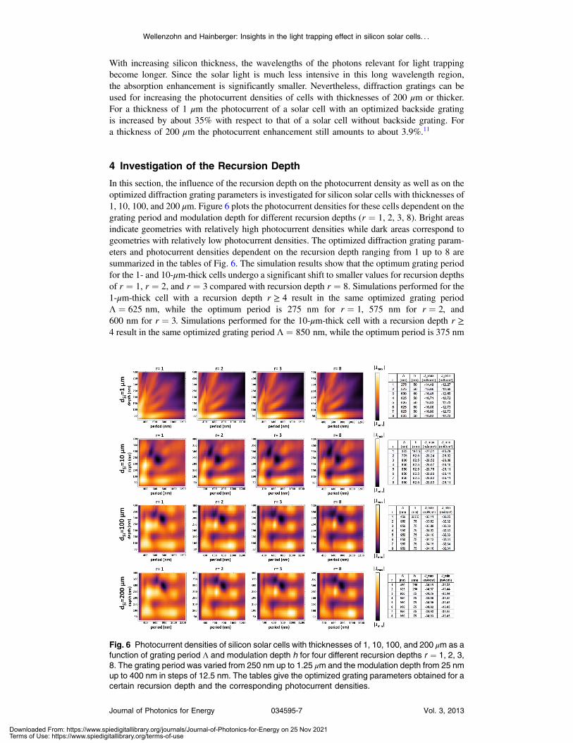
4 Investigation of the Recursion Depth
In this section, the influence of the recursion depth on the photocurrent density as well as on theoptimized diffraction grating parameters is investigated for silicon solar cells with thicknesses of1, 10, 100, and 200 μm. Figure 6 plots the photocurrent densities for these cells dependent on thegrating period and modulation depth for different recursion depths (r ¼ 1, 2, 3, 8). Bright areasindicate geometries with relatively high photocurrent densities while dark areas correspond togeometries with relatively low photocurrent densities. The optimized diffraction grating param-eters and photocurrent densities dependent on the recursion depth ranging from 1 up to 8 aresummarized in the tables of Fig. 6. The simulation results show that the optimum grating periodfor the 1- and 10-μm-thick cells undergo a significant shift to smaller values for recursion depthsof r ¼ 1, r ¼ 2, and r ¼ 3 compared with recursion depth r ¼ 8. Simulations performed for the1-μm-thick cell with a recursion depth r ≥ 4 result in the same optimized grating periodΛ ¼ 625 nm, while the optimum period is 275 nm for r ¼ 1, 575 nm for r ¼ 2, and600 nm for r ¼ 3. Simulations performed for the 10-μm-thick cell with a recursion depth r ≥4 result in the same optimized grating period Λ ¼ 850 nm, while the optimum period is 375 nm
Fig. 6 Photocurrent densities of silicon solar cells with thicknesses of 1, 10, 100, and 200 μm as afunction of grating period Λ and modulation depth h for four different recursion depths r ¼ 1, 2, 3,8. The grating period was varied from 250 nm up to 1.25 μm and the modulation depth from 25 nmup to 400 nm in steps of 12.5 nm. The tables give the optimized grating parameters obtained for acertain recursion depth and the corresponding photocurrent densities.
Wellenzohn and Hainberger: Insights in the light trapping effect in silicon solar cells. . .
Journal of Photonics for Energy 034595-7 Vol. 3, 2013
Downloaded From: https://www.spiedigitallibrary.org/journals/Journal-of-Photonics-for-Energy on 25 Nov 2021Terms of Use: https://www.spiedigitallibrary.org/terms-of-use

for r ¼ 1, 775 nm for r ¼ 2, and 800 nm for r ¼ 3. For the thicker cells with dSi ¼ 100 and200 μm, a recursion depth of r ¼ 3 is sufficient for identifying the optimum grating parameters.The difference in the optimized grating parameters for r ¼ 1 compared with r ¼ 8 can be aslarge as 500 nm for the period and 175 nm for the modulation depth.
The reason for the shift of the optimized grating period with increasing recursion depth is thata low recursion depth underestimates the contribution of longer wavelengths to absorption and,therefore, the potential of light trapping will not be fully exploited. A low recursion depth in thecombined RCWA/ray tracing simulation favors shorter wavelengths and consequently shortergrating periods. By including higher orders of recursion, the absorption of long wavelengthphotons increasingly contribute to the overall absorption. This relationship becomes apparentfrom Figs. 7(a)–7(c), which plot the absorption spectra of 1-, 10-, and 200-μm-thick siliconsolar cells with optimized gratings for recursion depths ranging from r ¼ 1 up to r ¼ 8. Forthe 1-μm-thick cell, differences in the simulated absorption curves occur already at wavelengthsof about 550 nm, where the solar spectrum has its maximum. For the 200-μm-thick cell devia-tions of the absorption, curves start to appear at much higher wavelengths near 1000 nm, whereintensity of the solar spectrum is much lower. For a recursion depth of r ¼ 8 the absorptionspectra and, thus, the photocurrent densities nearly converge. The absorption spectra forr ≥ 5 plotted in Figs. 7(a)–7(c) are almost indistinguishable, which suggests that a recursiondepth of r ¼ 5 is sufficient for in-depth analyses of the photocurrent densities. Simulations per-formed with r ¼ 8 require a significantly larger calculation capacity and therefore result inextremely long computation times. In our study, a recursion depth of r ¼ 5 turned out to providethe best compromise between accuracy in terms of grating optimization and computation time.The differences between the photocurrent densities for the optimized grating geometry calcu-lated with r ¼ 5 and r ¼ 8 amount to <0.1 mA∕cm2 for thin cells (dSi ¼ 1 μm), <0.07 mA∕cm2
for dSi ¼ 10 μm, and <0.03 mA∕cm2 for the thicker cells (dSi ¼ 200 μm).
Figures 7(d)–7(f) plot the photocurrent densities Jopt;r¼8ph of solar cells with optimized grating
geometries, which were obtained for a recursion depth of r ¼ 8 (black curves), as function of therecursion depth for the corresponding cell thicknesses 1, 10, and 200 μm. In order to emphasizethe importance of choosing a sufficiently high recursion depth the figures also include the photo-
current densities Jopt;r¼1ph and Jopt;r¼2
ph of solar cells with wrongly optimized grating parameters
obtained for r ¼ 1 (red curve) and r ¼ 2 (blue curve), respectively. With increasing recursion
depth the photocurrent densities Jopt;r¼8ph rise relatively more strongly and overtake the initially
Fig. 7 (a), (b), and (c) Absorption spectra of optimized diffraction gratings for 1, 10, and 200-μm-thick silicon solar cells with different recursion depths (r ¼ 1; : : : ; 8); (d), (e), and (f) photocurrentdensities of optimized gratings calculated by simulations with r ¼ 8 (black curves) as well as forgratings optimized with r ¼ 1 (red curves) and r ¼ 2 (blue curve) as a function of the recursiondepth.
Wellenzohn and Hainberger: Insights in the light trapping effect in silicon solar cells. . .
Journal of Photonics for Energy 034595-8 Vol. 3, 2013
Downloaded From: https://www.spiedigitallibrary.org/journals/Journal-of-Photonics-for-Energy on 25 Nov 2021Terms of Use: https://www.spiedigitallibrary.org/terms-of-use

higher values of Jopt;r¼1ph and Jopt;r¼2
ph . The differences of the calculated photocurrent densities
Jopt;r¼1ph and Jopt;r¼8
ph amount to 0.17 mA∕cm2 for the 1-μm-thick cell, to 0.62 mA∕cm2 for
dSi ¼ 10 − μm-thick cell, and to 0.6 mA∕cm2 for the 200-μm-thick cell. Optimizing the gratinggeometry with an insufficient recursion depth not only results in a lower theoretical photocurrentenhancement but also falsely predicts gratings with shorter periods and higher modulation depths(see tables in Fig. 6). From a practical point of view this puts higher technical demands on thefabrication process.
These results suggest that for the determination of the optimum diffraction grating design theproper choice of the recursion depth is highly important and that, in particular, simulations per-formed with a recursion depth of r ¼ 1 can lead to wrong optimized grating parameters not fullyexploiting the potential of the light trapping effect. This conclusion is of high relevance becauseother research groups limit their studies to a recursion depth of r ¼ 1, i.e., taking into accountonly the first backside diffraction at the gratings (e.g., Refs. 4, 10).
5 Investigation of the Diffraction Order
In this section, the influence of the number of diffraction orders on the optimized diffractiongrating parameters is investigated for silicon solar cells with 1, 10, and 200 μm thicknessfor a recursion depth of r ¼ 5. The simulation results shown in Figs. 4(a)–4(c) indicate thatconvergence is ensured if diffraction orders up to m ¼ �5 are taken into account. Moreover,from Eq. (2) it follows that the cut-off wavelength above which no diffraction can occur form > 5 becomes extremely short [compare also the cut-off wavelength of the fifth diffractionorder in Fig. 4(d)]. Therefore, contributions of these higher diffraction orders can be neglectedfor silicon solar cells. Figure 8 plots the photocurrent densities as functions of the grating periodΛ and the modulation depth h in dependence of the number of diffraction orders taken (up to�5)for different silicon thickness. The corresponding optimized grating parameters are given beloweach plot in Fig. 8. The results indicate that at least three diffraction orders for the 10- and200-μm-thick cells and four diffraction orders for the 1-μm-thick silicon solar cell have tobe included for the evaluation of the optimized diffraction gratings. Simulations performed
Fig. 8 Photocurrent densities of silicon solar cells with thicknesses of 1, 10, and 200 μm as afunction of grating period Λ and modulation depth h dependent on the diffraction orders up tom ¼ �5. These simulations were all performed with a recursion depth r ¼ 5.
Wellenzohn and Hainberger: Insights in the light trapping effect in silicon solar cells. . .
Journal of Photonics for Energy 034595-9 Vol. 3, 2013
Downloaded From: https://www.spiedigitallibrary.org/journals/Journal-of-Photonics-for-Energy on 25 Nov 2021Terms of Use: https://www.spiedigitallibrary.org/terms-of-use

with a lower number result in wrong optimized grating parameters with strongly reduced periodlengths.
6 Simulation Results for Oblique Light Incidence
So far, the optimization of silicon solar cells with backside diffraction gratings has only beeninvestigated for normally incident light. In the following, the influence of the angle of incidenceon the optimized grating parameters will be studied. For this purpose, a systematic optimizationof the grating geometry for angles of incidence on the solar cell of 0 deg to 70 deg was performedin 10 deg steps. For each angle of incidence, the period was varied from 0.25 to 1.25 μm and themodulation depth from 25 to 400 nm, both in steps of 12.5 nm. This optimization was carried outfor 1-, 10-, and 200-μm-thick silicon solar cells. The results showed that the optimized gratinggeometries do not depend on the angle of incidence. Figure 9 plots the photocurrent densities for1-, 10-, and 200-μm-thick silicon solar cells dependent on the period length and the modulationdepth for normally incident light as well as for Θin ¼ 60 deg. These figures clearly indicate thatthe optimized grating geometry does not depend on the angle of incidence on the solar cell. Thiscan be explained by the law of refraction and the high refractive index of silicon, which con-centrates all possible angles of incidence to the narrow escape cone inside silicon. Even sunlightshining on the solar cell under a glancing angle will hit the backside grating with a steep angle ofincidence below the ΘTIR, which is ≤ 16 deg for silicon [see red curve of Fig. 3(a)]. Since thediffraction efficiencies of backside gratings for normally incident photons, and photons hittingthe grating under small angles of a few degrees are very similar, they do not influence the opti-mized grating parameters.
Figures 9(g)–9(i) show the absorption spectra of 1-, 10-, and 200-μm-thick silicon solar cellswith optimized gratings for different angles of incidence starting from 0 deg up to 70 deg in stepsof 10 deg. Figures 10(a)–10(c) plot the corresponding optimized photocurrent densities as a
Fig. 9 (a)–(f) Photocurrent densities for 1, 10, and 200-μm-thick silicon solar cells as a function ofthe period and modulation depth for angles of incidence Θin ¼ 0 deg and Θin ¼ 60 deg; (g) and(h) absorption spectra of 1, 10, and 200-μm-thick silicon solar cells with optimized gratings forangles of incidence on the solar cell ranging from 0 deg to 70 deg in steps of 10 deg.
Wellenzohn and Hainberger: Insights in the light trapping effect in silicon solar cells. . .
Journal of Photonics for Energy 034595-10 Vol. 3, 2013
Downloaded From: https://www.spiedigitallibrary.org/journals/Journal-of-Photonics-for-Energy on 25 Nov 2021Terms of Use: https://www.spiedigitallibrary.org/terms-of-use

function of the angle of incidence. Since the incident sunlight flux passing through a unit surfacearea of a solar cell decreases with the cosine of the angle of incidence, the resulting photocurrentdensity Jph;gratðΘinÞ should show a similar behavior. The thin green colored lines in Fig. 10represent this limiting case given by
Jph;gratðΘinÞ ¼ Jph;gratðΘin ¼ 0Þ cosðΘinÞ: (4)
For angles Θin ≤ 40 deg the optimized photocurrent densities are in good agreement withthis equation. For angles Θin > 40 deg, the calculated photocurrent densities more and moredeviate from this characteristic primarily due to the increase of front side reflection lossesbecause the SiNx AR coating is optimized for normally incident light.
7 Conclusion
In this article, we employed a simulation approach that combines ray tracing with RCWA, whichenables a strongly reduced computation time and a gain in simulation precision compared tofully electromagnetic simulation methods, such as RCWA or FDTD for solar cells thickerthan ∼10 μm. This approach also provided a much better physical insight into the light trappingmechanism of silicon solar cells with backside diffraction gratings. In contrast to fully electro-magnetic simulation methods, characteristic humps in the absorption spectra can be observedthat are directly related to the light trapping mechanism. We provided a detailed analysis andexplanation for the origin of these characteristic humps in the absorption spectra, which helps inunderstanding the underlying light trapping mechanism in silicon solar cells with backside dif-fraction gratings.
In addition, in this article, an in-depth analysis of the influence of the two determinant sim-ulation parameters—the recursion depth and the diffraction order—on the simulation results wasinvestigated. The results showed that for the optimum diffraction grating design, the properchoice of the recursion depth is of significant importance. Dependent on the silicon thicknessthe recursion depth r must exceed a certain minimum value. While for 200-μm-thick solar cellsat least two backside reflections/diffractions, i.e., r ¼ 3 must be taken into account, for 1-μm-thin cells a recursion depth of r ¼ 4 is necessary. Therefore, simulations taking into account onlythe first backside diffraction (r ¼ 1) result in wrongly optimized grating parameters with sig-nificantly shorter periods, which do not fully exploit the light trapping effect and, thus, have alower photocurrent density improvement. A recursion depth of r ¼ 5 turned out to be the besttrade-off between simulation time and precision of the calculated photocurrent densities, for allinvestigated cell thicknesses ranging from 1 to 200 μm. With respect to the diffraction order, theanalysis indicates that for silicon solar cells an inclusion of diffraction orders up to m ¼ �5 issufficient to obtain correct simulation results.
Furthermore, in this article, for the first time to the best of our knowledge, it was shown thatthe angle of incidence does not influence the optimum diffraction grating parameters for a givensilicon thickness. Therefore, the optimization of silicon solar cells with backside diffraction gra-tings and planar front side AR coatings can be performed for normal light incidence.
Fig. 10 (a)–(c) Maximum photocurrent densities (black dots) for 1, 10, and 200-μm-thick siliconsolar cells as a function of the angle of incidence. The green curves indicate the photocurrentdensities resulting from the values for normally incident light multiplied with the cosine of theangle of incidence.
Wellenzohn and Hainberger: Insights in the light trapping effect in silicon solar cells. . .
Journal of Photonics for Energy 034595-11 Vol. 3, 2013
Downloaded From: https://www.spiedigitallibrary.org/journals/Journal-of-Photonics-for-Energy on 25 Nov 2021Terms of Use: https://www.spiedigitallibrary.org/terms-of-use

Acknowledgments
This work was supported by the Austrian NANO Initiative under the grant PLATON Si solar(project no. 819660).
References
1. P. Sheng, A. N. Bloch, and R. S. Stepleman, “Wavelength-selective absorption enhancementin thin-film solar cells,” Appl. Phys. Lett. 43(6), 579–581 (1983), http://dx.doi.org/10.1063/1.94432.
2. C. Heine and R. H. Morf, “Submicrometer gratings for solar energy applications,” Appl.Opt. 34(14), 2476–2482 (1995), http://dx.doi.org/10.1364/AO.34.002476.
3. S. H. Zaidi, J. M. Gee, and D. S. Ruby, “Diffraction grating structures in solar cells,” in 28thIEEE Photovoltaic Spec. Conf., pp. 395–398 (2000).
4. P. Voisin et al., “Nanostructured back side silicon solar cells,” in 24th European PVSolar Energy Conf. and Exhibition, paper 2DV.1.4., WIP–Renewable Energies, Munich(2009).
5. R. Dewan and D. Knipp,” Light trapping in thin-film silicon solar cells with integrateddiffraction grating,” J. Appl. Phys. 106(8), 074901 (2009), http://dx.doi.org/10.1063/1.3232236.
6. N. N. Feng et al., “Design of highly efficient light-trapping structures for thin-film crys-talline silicon solar cells,” IEEE Trans. Electron. Dev. 54(8), 1926–1933 (2007), http://dx.doi.org/10.1109/TED.2007.900976.
7. P. Bermel et al., “Improving thin-film crystalline silicon solar cell efficiencies with photoniccrystals,” Opt. Exp. 15(25), 16986–17000 (2007), http://dx.doi.org/10.1364/OE.15.016986.
8. L. Zeng et al., “Demonstration of enhanced absorption in thin film Si solar cells with tex-tured photonic crystal back reflector,” Appl. Phys. Lett. 93(22), 221105 (2008), http://dx.doi.org/10.1063/1.3039787.
9. J. G. Mutitu et al., “Thin film solar cell design based on photonic crystal and diffractivegrating structures,” Opt. Exp. 16(19), 15238–15248 (2008), http://dx.doi.org/10.1364/OE.16.015238.
10. R. Rothemund et al.,” Light trapping in monocrystalline Si solar cells using back-side dif-fraction gratings,” Solid State Phenom. 178–179, 446–450 (2011), http://dx.doi.org/10.4028/www.scientific.net/SSP.178-179.
11. M. Wellenzohn and R. Hainberger, “Light trapping by backside diffraction gratings in sil-icon solar cells revisited,” Opt. Exp. 20(S1), A20–A27 (2012), http://dx.doi.org/10.1364/OE.20.000A20.
12. M. Wellenzohn and R. Hainberger, “Optimization of silicon solar cells using backside dif-fraction gratings,” in Renewable Energy, and the Environment, OSATechnical Digest (CD)Optical Society of America, Washington, D.C, paper PWC2 (2011).
13. M. Wellenzohn and R. Hainberger, “A 2D numerical study of the photo current densityenhancement in silicon solar cells with optimized backside gratings,” in 37th IEEEPhotovoltaic Spec. Conf., pp. 002963–002967 (2011).
14. M. Born and E. Wolf, Principles of Optics 7th ed., pp. 61–66, Cambridge University Press,New York (1999).
15. M. A. Green and M. J. Keevers, “Optical properties of intrinsic silicon at 300 K,” Prog.Photovolt. Res. Appl. 3(3), 189–192 (1995), http://dx.doi.org/10.1002/(ISSN)1099-159X.
16. http://refractiveindex.info (7 June 2013).17. A. D. Rakic, “Algorithm for the determination of intrinsic optical constants of metal films:
application to aluminum,” Appl. Opt. 34(22), 4755–4767 (1995), http://dx.doi.org/10.1364/AO.34.004755.
18. I. H. Malitson, “Interspecimen comparison of the refractive index of fused silica,” J. Opt.Soc. Am. 55(10), 1205–1208 (1965), http://dx.doi.org/10.1364/JOSA.55.001205.
19. DiffractMOD, www.rsoftdesign.com (7 June 2013).20. A. Donges, “The coherence length of black-body radiation,” Eur. J. Phys. 19(3), 245–249
(1998), http://dx.doi.org/10.1088/0143-0807/19/3/006.
Wellenzohn and Hainberger: Insights in the light trapping effect in silicon solar cells. . .
Journal of Photonics for Energy 034595-12 Vol. 3, 2013
Downloaded From: https://www.spiedigitallibrary.org/journals/Journal-of-Photonics-for-Energy on 25 Nov 2021Terms of Use: https://www.spiedigitallibrary.org/terms-of-use

21. C. R. Wheeler, R. D. Ramsier, and P. N. Henriksen, “An investigation of the temporal coher-ence length of light,” Eur. J. Phys. 24(4), 443–450 (2003), http://dx.doi.org/10.1088/0143-0807/24/4/363.
22. G. R. Reider, Photonik, Eine Einführung in die Grundlagen, p. 31, Springer-Verlag, Wien(2004).
Markus Wellenzohn was born in Zams (Tyrol), Austria. He received theDipl.-Ing. degree in physics from the Vienna University of Technology,Austria, in 2008. Since 2007 he has been working as a Junior Scientistfor the AITAustrian Institute of Technology GmbH. His research activitieshave been mainly related to silicon nanophotonics, where he focused onthe simulation and design of photonic crystal sensors for optical biosensingas well as on light management for photovoltaics.
Rainer Hainberger was born in Vienna, Austria. He received the Dipl.-Ing. degree in physics from the Vienna University of Technology, Austria,in 1995 and the PhD degree in electrical engineering from the University ofTokyo, Japan, in 2000. From 2000 to 2004 he was affiliated with FujitsuLaboratories Ltd., Japan, where he was working on Raman amplification inWDM transmission systems and all-optical signal processing includingtopics such as 2R regeneration and highly nonlinear photonic crystal fibers.Since 2004 he has been working for the AIT Austrian Institute ofTechnology GmbH. His research activities have been mainly related to
optical biosensing employing silicon and polymer photonic concepts. Apart from that he hasalso been involved in research projects related to light management for photovoltaics.
Wellenzohn and Hainberger: Insights in the light trapping effect in silicon solar cells. . .
Journal of Photonics for Energy 034595-13 Vol. 3, 2013
Downloaded From: https://www.spiedigitallibrary.org/journals/Journal-of-Photonics-for-Energy on 25 Nov 2021Terms of Use: https://www.spiedigitallibrary.org/terms-of-use