


Languages
Pages
Legal

LTC3722-1/LTC3722-2
1372212fb
For more information www.linear.com/LTC3722
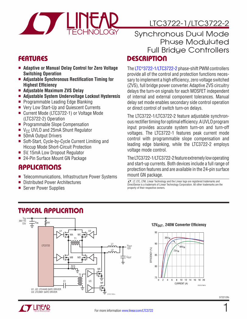
TYPICAL APPLICATION
FEATURES DESCRIPTION
Synchronous Dual Mode Phase Modulated
Full Bridge Controllers
The LTC®3722-1/LTC3722-2 phase-shift PWM controllers provide all of the control and protection functions neces-sary to implement a high efficiency, zero voltage switched (ZVS), full bridge power converter. Adaptive ZVS circuitry delays the turn-on signals for each MOSFET independent of internal and external component tolerances. Manual delay set mode enables secondary side control operation or direct control of switch turn-on delays.
The LTC3722-1/LTC3722-2 feature adjustable synchron-ous rectifier timing for optimal efficiency. A UVLO program input provides accurate system turn-on and turn-off voltages. The LTC3722-1 features peak current mode control with programmable slope compensation and leading edge blanking, while the LTC3722-2 employs voltage mode control.
The LTC3722-1/LTC3722-2 feature extremely low operating and start-up currents. Both devices include a full range of protection features and are available in the 24-pin surface mount GN package.
12VOUT, 240W Converter Efficiency
APPLICATIONS
n Adaptive or Manual Delay Control for Zero Voltage Switching Operation
n Adjustable Synchronous Rectification Timing for Highest Efficiency
n Adjustable Maximum ZVS Delayn Adjustable System Undervoltage Lockout Hysteresisn Programmable Leading Edge Blankingn Very Low Start-Up and Quiescent Currentsn Current Mode (LTC3722-1) or Voltage Mode
(LTC3722-2) Operationn Programmable Slope Compensationn VCC UVLO and 25mA Shunt Regulatorn 50mA Output Driversn Soft-Start, Cycle-by-Cycle Current Limiting and
Hiccup Mode Short-Circuit Protectionn 5V, 15mA Low Dropout Regulatorn 24-Pin Surface Mount GN Package
n Telecommunications, Infrastructure Power Systemsn Distributed Power Architecturesn Server Power Supplies
L, LT, LTC, LTM, Linear Technology and the Linear logo are registered trademarks and DirectSense is a trademark of Linear Technology Corporation. All other trademarks are the property of their respective owners.
CIN R1
LTC3722
VIN36V TO
72V
MA
ME
MF
MB
MC
MD
U1 U2
U3
L1
L2
RCS
T1
T2
C1
VOUT12V
COUT
372212 TA01a
U1, U2: LTC4440 GATE DRIVERU3: LTC3901 GATE DRIVER
CURRENT (A)0
EFFI
CIEN
CY (%
)
95
90
85
80
7516
372212 TA01b
42 6 10 14 188 12 20
36VIN
72VIN
48VIN

LTC3722-1/LTC3722-2
2372212fb
For more information www.linear.com/LTC3722
ABSOLUTE MAXIMUM RATINGSVCC to GND (Low Impedance Source) ........ –0.3V to 10V (Chip Self Regulates at 10.3V)UVLO to GND ..............................................–0.3V to VCCAll Other Pins to GND (Low Impedance Source) .......................... –0.3V to 5.5VVCC (Current Fed) ...................................................25mA
(Note 1)
PIN CONFIGURATION
ORDER INFORMATIONLEAD FREE FINISH TAPE AND REEL PART MARKING PACKAGE DESCRIPTION TEMPERATURE RANGE
LTC3722EGN-1#PBF LTC3722EGN-1#TRPBF LTC3722EGN-1 24-Lead Plastic SSOP –40°C to 85°C
LTC3722EGN-2#PBF LTC3722EGN-2#TRPBF LTC3722EGN-2 24-Lead Plastic SSOP –40°C to 85°C
LTC3722IGN-1#PBF LTC3722IGN-1#TRPBF LTC3722IGN-1 24-Lead Plastic SSOP –40°C to 85°C
LTC3722IGN-2#PBF LTC3722IGN-2#TRPBF LTC3722IGN-2 24-Lead Plastic SSOP –40°C to 85°C
LTC3722HGN-1#PBF LTC3722HGN-1#TRPBF LTC3722HGN-1 24-Lead Plastic SSOP –40°C to 150°C
Consult LTC Marketing for parts specified with wider operating temperature ranges. Consult LTC Marketing for information on non-standard lead based finish parts.For more information on lead free part marking, go to: http://www.linear.com/leadfree/ For more information on tape and reel specifications, go to: http://www.linear.com/tapeandreel/
VREF Output Current ................................. Self RegulatedOutputs (A, B, C, D, E, F) Current ....................... ±100mA Operating Junction Temperature Range (Note 6) .................................................. –40°C to 150°CStorage Temperature Range .................. –65°C to 150°CLead Temperature (Soldering, 10 sec) ................... 300°C
LTC3722-1 LTC3722-2
1
2
3
4
5
6
7
8
9
10
11
12
TOP VIEW
GN PACKAGE24-LEAD NARROW PLASTIC SSOP
24
23
22
21
20
19
18
17
16
15
14
13
SYNC
DPRG
CS
COMP
RLEB
FB
SS
NC
PDLY
SBUS
ADLY
UVLO
CT
GND
PGND
OUTA
OUTB
OUTC
VCC
OUTD
OUTE
OUTF
VREF
SPRG
TJMAX = 125°C, θJA = 100°C/W
1
2
3
4
5
6
7
8
9
10
11
12
TOP VIEW
GN PACKAGE24-LEAD NARROW PLASTIC SSOP
24
23
22
21
20
19
18
17
16
15
14
13
SYNC
RAMP
CS
COMP
DPRG
FB
SS
NC
PDLY
SBUS
ADLY
UVLO
CT
GND
PGND
OUTA
OUTB
OUTC
VCC
OUTD
OUTE
OUTF
VREF
SPRG
TJMAX = 125°C, θJA = 100°C/W

LTC3722-1/LTC3722-2
3372212fb
For more information www.linear.com/LTC3722
ELECTRICAL CHARACTERISTICS
SYMBOL PARAMETER CONDITIONS MIN TYP MAX UNITS
Input Supply
VCCUV VCC Under Voltage Lockout Measured on VCC 10.25 10.5 V
VCCHY VCC UVLO Hysteresis Measured on VCC 3.8 4.2 V
ICCST Start-Up Current VCC = VUVLO – 0.3V LTC3722E-1/LTC3722I-1/LTC3722E-2/LTC3722I-2 LTC3722H-1
l
l
145 145
230 250
µA µA
ICCRN Operating Current No Load on Outputs 5 8 mA
VSHUNT Shunt Regulator Voltage Current into VCC = 10mA 10.3 10.8 V
RSHUNT Shunt Resistance Current into VCC = 10mA to 17mA 1.1 3.5 Ω
SUVLO System UVLO Threshold Measured on UVLO Pin, 10mA into VCC 4.8 5.0 5.2 V
SHYST System UVLO Hysteresis Current Current Flows Out of UVLO Pin 8.5 10 11.5 µA
Delay Blocks
DTHR Delay Pin Threshold ADLY and PDLY
SBUS = 1.5V SBUS = 2.25V
l
l
1.4 2.1
1.5 2.25
1.6 2.4
V V
DHYS Delay Hysteresis Current ADLY and PDLY
SBUS = 1.5V, ADLY/PDLY = 1.7V 1.3 mA
DTMO Delay Timeout RDPRG = 60.4K 100 ns
DFXT Fixed Delay Threshold Measured on SBUS 4 V
DFTM Fixed Delay Time SBUS = VREF , ADLY, PDLY = 1V 70 ns
Phase Modulator
ICS CS Discharge Current CS = 1V, COMP = 0V, CT = 4V, LTC3722-1 Only
50 mA
ISLP Slope Compensation Current Measured on CS, CT = 1V CT = 2.25V
30 68
µA µA
DCMAX Maximum Phase Shift COMP = 4.5V l 95 98.5 %
DCMIN Minimum Phase Shift COMP = 0V l 0 0.5 %
Oscillator
OSCI Initial Accuracy TA = 25°C, CT = 270pF 225 250 275 kHz
OSCT Total Variation VCC = 6.5V to 9.5V l 215 250 285 kHz
OSCV CT Ramp Amplitude Measured on CT 2.2 V
OSYT SYNC Threshold Measured on SYNC 1.6 1.9 2.2 V
OSYW Minimum SYNC Pulse Width Measured at Outputs (Note 2) 100 ns
OSYR SYNC Frequency Range Measured at Outputs (Note 2) 1000 kHz
Error Amplifier
VFB FB Input Voltage COMP = 2.5V (Note 4) 1.172 1.204 1.236 V
FBI FB Input Range Measured on FB (Note 5) –0.3 2.5 V
AVOL Open-Loop Gain COMP = 1V to 3V (Note 4) 70 90 dB
IIB Input Bias Current COMP = 2.5V (Note 4) 5 20 nA
VOH Output High Load on COMP = –100µA 4.7 4.92 V
VOL Output Low Load on COMP = 100µA 0.18 0.4 V
ISOURCE Output Source Current COMP = 2.5V 400 800 µA
ISINK Output Sink Current COMP = 2.5V 2 5 mA
The l denotes the specifications which apply over the specified operating junction temperature range, otherwise specifications are at TA = 25°C. VCC = 9.5V, CT = 270pF, RDPRG = 60.4k, RSPRG = 100k, unless otherwise noted (Note 6).
LTC3722-1/LTC3722-2
4372212fb
For more information www.linear.com/LTC3722
Note 1: Stresses beyond those listed under Absolute Maximum Ratings may cause permanent damage to the device. Exposure to any Absolute Maximum Rating condition for extended periods may affect device reliability and lifetime.Note 2: Sync amplitude = 5VP-P , pulse width = 50ns. Verify output (A-F) frequency = one-half sync frequency.Note 3: Includes leading edge blanking delay, RLEB = 20k.Note 4: FB is driven by a servo-loop amplifier to control VCOMP for these tests.Note 5: Set FB to –0.3V, 2.5V and insure that COMP does not phase invert.Note 6: The LTC3722 is tested under pulsed load condition such that TJ ≈ TA. The LTC3722E-1/LTC3722E-2 are guaranteed to meet performance specifications from 0°C to 85°C. Specifications over the –40°C to 85°C operating junction temperature range are assured by design,
SYMBOL PARAMETER CONDITIONS MIN TYP MAX UNITS
Reference
VREF Initial Accuracy TA = 25°C, Measured on VREF 4.925 5.00 5.075 V
REFLD Load Regulation Load on VREF = 100µA to 5mA 2 15 mV
REFLN Line Regulation VCC = 6.5V to 9.5V 0.9 10 mV
REFTV Total Variation Line, Load l 4.900 5.000 5.100 V
REFSC Short-Circuit Current VREF Shorted to GND 18 30 45 mA
Outputs
OUTH(x) Output High Voltage IOUT(x) = –50mA 7.9 8.4 V
OUTL(x) Output Low Voltage IOUT(x) = 50mA 0.6 1 V
RHI(x) Pull-Up Resistance IOUT(x) = –50mA to –10mA 22 30 Ω
RLO(x) Pull-Down Resistance IOUT(x) = –50mA to –10mA 12 20 Ω
tr(x) Rise Time COUT(x) = 50pF (Note 8) 5 15 ns
tf(x) Fall Time COUT(x) = 50pF (Note 8) 5 15 ns
SDEL SYNC Driver Turn-0ff Delay RSPRG = 100k 180 ns
Current Limit and Shutdown
CLPP Pulse by Pulse Current Limit Threshold Measured on CS LTC3722E-1/LTC3722I-1/LTC3722E-2/LTC3722I-2 LTC3722H-1
270 270
300 300
330 340
mV mV
CLSD Shutdown Current Limit Threshold Measured on CS 0.55 0.65 0.73 V
CLDEL Current Limit Delay to Output 100mV Overdrive on CS (Notes 3, 7) 80 ns
SSI Soft-Start Current SS = 2.5V 7 12 17 µA
SSR Soft-Start Reset Threshold Measured on SS 0.7 0.4 0.1 V
FLT Fault Reset Threshold Measured on SS 4.5 3.9 3.5 V
The l denotes the specifications which apply over the specified operating junction temperature range, otherwise specifications are at TA = 25°C. VCC = 9.5V, CT = 270pF, RDPRG = 60.4k, RSPRG = 100k, unless otherwise noted (Note 6).
characterization and correlation with statistical process controls. The LTC3722I-1/LTC3722I-2 are guaranteed over the –40°C to 85°C operating junction temperature range and the LTC3722H-1 is guaranteed over the –40°C to 150°C operating junction temperature range.High junction temperatures degrade operating lifetimes; operating lifetime is derated for junction temperatures greater than 125°C. Note that the maximum ambient temperature consistent with these specifications is determined by specific operating conditions in conjunction with board layout, the rated package thermal impedance and other environmental factors. Note 7: Guaranteed by design, not tested in production.Note 8: Rise time is measured from the 10% to 90% points of the rising edge of the driver output signal. Fall time is measured from the 90% to 10% points of the falling edge of the driver output signal.
ELECTRICAL CHARACTERISTICS

LTC3722-1/LTC3722-2
5372212fb
For more information www.linear.com/LTC3722
TYPICAL PERFORMANCE CHARACTERISTICS
Leading Edge Blanking Time vs RLEB VREF vs IREF VREF vs Temperature
Error Amplifier Gain/Phase Start-Up ICC vs TemperatureDelay Hysteresis Current vs Temperature
Start-Up ICC vs VCC VCC vs ISHUNT
Oscillator Frequency vs Temperature
VCC (V)0
I CC
(µA)
100
150
8
372212 G01
50
02 4 6 10
200TA = 25°C
ISHUNT (mA)0
V CC
(V)
10.00
10.25
40
372212 G02
9.75
9.5010 20 30 50
10.50TA = 25°C
RLEB (k)0
BLAN
K TI
ME
(ns)
350
300
250
200
150
100
50
0
372212 G04
40 1002010 30 50 70 9060 80
TA = 25°C
IREF (mA)0
V REF
(V)
5.05
5.00
4.95
4.90
4.85
4.8015 25 40
372212 G05
5 10 20 30 35
TA = 25°C
TA = 85°C
TA = –40°C
FREQUENCY (Hz)
GAIN
(dB)
PHAS
E (D
EG) –180
1M
372212 G07
–270
–360
10 1k100 10k 100k 10M
100806040200
TA = 25°C
TEMPERATURE (°C)
230
FREQ
UENC
Y (k
Hz)
240
250
260
–10 30 70 110
372212 G03
150–30–50 10 50 90 130
CT = 270pF
TEMPERATURE (°C)–50
V REF
(V) 4.99
5.00
5.01
110
372212 G06
4.98
4.97
4.96–30 –10 10 30 50 70 90 130 150
TEMPERATURE (°C)–60
100
I CC
(µA)
110
130
140
150
60
190
372212 G08
120
0–30 90 12030 150
160
170
180
TEMPERATURE (°C)–60
HYST
ERES
IS C
URRE
NT (m
A)
1.286
1.298
1.300
1.302
0 60 90
372212 G09
1.282
1.294
1.290
1.284
1.296
1.280
1.292
1.288
–30 30 120 150
SBUS = 1.5V

LTC3722-1/LTC3722-2
6372212fb
For more information www.linear.com/LTC3722
TYPICAL PERFORMANCE CHARACTERISTICS
FB Input Voltage vs Temperature Delay Timeout vs RDPRG
ZVS Delay in Fixed Mode, SBUS = 5V
Synchronous Driver Turn-Off Delay in Fixed Mode
Synchronous Driver Turn-Off Delay in Adaptive Mode, SBUS = 1.5V
Slope Current vs Temperature VCC Shunt Voltage vs TemperatureDelay Pin Threshold vs Temperature
RDPRG (kΩ)10
0
DELA
Y (n
s)
50
100
150
200
300
60 110 160 210
372212 G14
260 310
250
SBUS = 1.125V
SBUS = 2.25V
TA = 25°C
SBUS = 1.5V
RDPRG (kΩ)10
0
DELA
Y (n
s)
50
100
150
200
300
60 110 160 210
372212 G15
260 310
250
ADLY = PDLY = 1.125V
ADLY = PDLY = 2.25VADLY = PDLY = 1.5V
TA = 25°C
RSPRG (kΩ)10
200
250
350
160
372212 G16
150
100
60 110 210
50
0
300
DELA
Y (n
S)
TA = 25°C
RSPRG (kΩ)10
20
DELA
Y (n
s)
100
140
180
260
30 110 150
372212 G17
60
220
90 19050 70 130 170
B HI-F LOW
A HI-E LOW
TA = 25°C
TEMPERATURE (°C)–60
0
CURR
ENT
(µA)
10
30
40
50
60
90
372212 G10
20
0–30 90 12030 150
60
70
80 CT = 2.25V
CT = 1V
TEMPERATURE (°C)–60
10.2
10.3
10.5
30 90
372212 G11
10.1
10.0
–30 0 60 120 150
9.9
9.8
10.4
SHUN
T VO
LTAG
E (V
)
ICC = 10mA
TEMPERATURE (°C)–60
1.4
THRE
SHOL
D (V
)
1.5
1.7
1.8
1.9
2.4
2.1
0 60 90 120
372212 G12
1.6
2.2
2.3
2.0
–30 30 150
SBUS = 2.25V
SBUS = 1.5V
TEMPERATURE (°C)–60
FB V
OLTA
GE (V
)
1.209
30
372212 G13
1.206
1.204
–30 0 60
1.203
1.202
1.210
1.208
1.207
1.205
90 120 150

LTC3722-1/LTC3722-2
7372212fb
For more information www.linear.com/LTC3722
PIN FUNCTIONSSYNC (Pin 1/Pin 1): Synchronization Input/Output for the Oscillator. The input threshold for SYNC is approximately 1.9V, making it compatible with both CMOS and TTL logic. Terminate SYNC with a 5.1k resistor to GND.
DPRG (Pin 2/Pin 5): Programming Input for Default Zero Voltage Transition (ZVS) Delay. Connect a resistor from DPRG to VREF to set the maximum turn on delay for outputs A, B, C, D. The nominal voltage on DPRG is 2V.
RAMP (NA/Pin 2): Input to Phase Modulator Comparator for LTC3722-2 only. The voltage on RAMP is internally level shifted by 650mV.
CS (Pin 3/Pin 3): Input to Phase Modulator for the LTC3722-1. Input to pulse-by-pulse and overload current limit comparators, output of slope compensation circuitry. The pulse by pulse comparator has a nominal 300mV threshold, while the overload comparator has a nominal 650mV threshold.
COMP (Pin 4/Pin 4): Error Amplifier Output, Inverting Input to Phase Modulator.
RLEB (Pin 5/NA): Timing Resistor for Leading Edge Blank-ing. Use a 10k to 100k resistor to program from 40ns to 310ns of leading edge blanking of the current sense signal on CS for the LTC3722-1. A ±1% tolerance resistor is recommended. The LTC3722-2 has a fixed blanking time of approximately 80ns.
FB (Pin 6/Pin 6): Error Amplifier Inverting Input. This is the voltage feedback input for the LTC3722. The nominal regulation voltage at FB is 1.204V.
SS (Pin 7/Pin 7): Soft-Start/Restart Delay Circuitry Timing Capacitor. A capacitor from SS to GND provides a controlled ramp of the current command (LTC3722-1), or duty cycle (LTC3722-2). During overload conditions SS is discharged to ground initiating a soft-start cycle.
NC (Pin 8/Pin 8): No Connection. Tie this pin to GND.
PDLY (Pin 9/Pin 9): Passive Leg Delay Circuit Input. PDLY is connected through a voltage divider to the left leg of the bridge in adaptive ZVS mode. In fixed ZVS mode, a voltage between 0V and 2.5V on PDLY, programs a fixed ZVS delay time for the passive leg transition.
SBUS (Pin 10/Pin 10): Line Voltage Sense Input. SBUS is connected to the main DC voltage feed by a resistive volt-age divider when using adaptive ZVS control. The voltage divider is designed to produce 1.5V on SBUS at nominal VIN. If SBUS is tied to VREF , the LTC3722-1/LTC3722-2 is configured for fixed mode ZVS control.
ADLY (Pin 11/Pin 11): Active Leg Delay Circuit Input. ADLY is connected through a voltage divider to the right leg of the bridge in adaptive ZVS mode. In fixed ZVS mode, a voltage between 0V and 2.5V on ADLY, programs a fixed ZVS delay time for the active leg transition.
UVLO (Pin 12/Pin 12): Input to Program System Turn-On and Turn-Off Voltages. The nominal threshold of the UVLO comparator is 5V. UVLO is connected to the main DC system feed through a resistor divider. When the UVLO threshold is exceeded, the LTC3722-1/LTC3722-2 commences a soft-start cycle and a 10µA (nominal) cur-rent is fed out of UVLO to program the desired amount of system hysteresis. The hysteresis level can be adjusted by changing the resistance of the divider.
SPRG (Pin 13/Pin 13): A resistor is connected between SPRG and GND to set the turn-off delay for the synchronous rectifier driver outputs (OUTE and OUTF). The nominal voltage on SPRG is 2V.
VREF (Pin 14/Pin 14): Output of the 5V Reference. VREF is capable of supplying up to 18mA to external circuitry. VREF should be decoupled to GND with a 1µF ceramic capacitor.
OUTF (Pin 15/Pin 15): 50mA Driver for Synchronous Rectifier Associated with OUTB and OUTC.
OUTE (Pin 16/Pin 16): 50mA Driver for Synchronous Rectifier Associated with OUTA and OUTD.
OUTD (Pin 17/Pin 17): 50mA Driver for Low Side of the Full Bridge Active Leg.
VCC (Pin 18/Pin 18): Supply Voltage Input to the LTC3722-1/LTC3722-2 and 10.25V Shunt Regulator. The chip is enabled after VCC has risen high enough to allow the VCC shunt regulator to conduct current and the UVLO comparator threshold is exceeded. Once the VCC shunt regulator has turned on, VCC can drop to as low as 6V (typ) and maintain operation.
(LTC3722-1/LTC3722-2)

LTC3722-1/LTC3722-2
8372212fb
For more information www.linear.com/LTC3722
BLOCK DIAGRAM
PIN FUNCTIONS (LTC3722-1/LTC3722-2)
OUTC (Pin 19/Pin 19): 50mA Driver for High Side of the Full Bridge Active Leg.
OUTB (Pin 20/Pin 20): 50mA Driver for Low Side of the Full Bridge Passive Leg.
OUTA (Pin 21/Pin 21): 50mA Driver for High Side of the Full Bridge Passive Leg.
PGND (Pin 22/Pin 22): Power Ground for the LTC3722. The output drivers of the LTC3722 are referenced to PGND. Connect the ceramic VCC bypass capacitor di- rectly to PGND.
GND (Pin 23/Pin 23): All circuits other than the output drivers in the LTC3722 are referenced to GND. Use of a ground plane is recommended but not absolutely neces-sary.
CT (Pin 24/Pin 24): Timing Capacitor for the Oscillator. Use a ±5% or better low ESR ceramic capacitor for best results.
LTC3722-1 Current Mode SYNC Phase-Shift PWM
OUTE
OUTF
OUTC
OUTD
ADLY
PGND
PDLY
OUTA
OUTB
372212 BD01
–
+
–
+ –
+
–
+
–
+3
7
6
18 12 14
17
11
22
19
15
16
20
9
21
24
23
1 13 102
4
5
VCC UVLO
10.25V = ON6V = OFF
5VREF AND LDO
1.2VREF GOOD
FAULTLOGIC
SHUTDOWNCURRENT
LIMIT
PULSE BY PULSECURRENT LIMIT
650mV
SLOPECOMPENSATION
CT/R
BLANK
SS
CS
RLEB
QB
Q
R
S QBR
S
R214.9k
M120Ω VREF
1.2V 5V
+
–650mV
R150k
PHASEMODULATOR
ERRORAMPLIFIER
FB
COMP
12µA
300mV
VCCGOOD
1 = ENABLE0 = DISABLE
OSC
ACTIVEDELAY
SYNCRECTIFIER
DRIVELOGIC
PASSIVEDELAY
QB
QT
VCC UVLO VREF CT SYNC SPRG SBUSDPRG
GND
SYSTEMUVLO
M2

LTC3722-1/LTC3722-2
9372212fb
For more information www.linear.com/LTC3722
BLOCK DIAGRAMLTC3722-2 Voltage Mode SYNC Phase-Shift PWM
OUTE
OUTF
OUTC
OUTD
ADLY
PGND
PDLY
OUTA
OUTB
372212 BD02
–
+
–
+ –
+
–
+
–
+3
7
6
18 12 14
17
11
22
19
15
16
20
9
21
24
23
1 13 105
4
VCC UVLO
10.25V = ON6V = OFF
5VREF AND LDO
1.2VREF GOOD
FAULTLOGIC
SHUTDOWNCURRENT
LIMIT
PULSE BY PULSECURRENT LIMIT
650mV
BLANK
SS
2
RAMP
CS
QB
Q
R
S QBR
S
VREF
1.2V 5V
+–650mV
R150k
PHASEMODULATOR
ERRORAMPLIFIER
FB
COMP
12µA
300mV
VCCGOOD
1 = ENABLE0 = DISABLE
OSC
ACTIVEDELAY
SYNCRECTIFIER
DRIVELOGIC
PASSIVEDELAY
QB
QT
VCC UVLO VREF CT SYNC SPRG SBUSDPRG
GND
SYSTEMUVLO
M2

LTC3722-1/LTC3722-2
10372212fb
For more information www.linear.com/LTC3722
OPERATIONPhase-Shift Full Bridge PWM
Conventional full bridge switching power supply topologies are often employed for high power, isolated DC/DC and off-line converters. Although they require two additional switching elements, substantially greater power and higher efficiency can be attained for a given transformer size compared to the more common single-ended forward and flyback converters. These improvements are realized since the full bridge converter delivers power during both parts of the switching cycle, reducing transformer core loss and lowering voltage and current stresses. The full bridge converter also provides inherent automatic transformer flux reset and balancing due to its bidirectional drive configuration. As a result, the maximum duty cycle range is extended, further improving efficiency. Soft-switching variations on the full bridge topology have been proposed to improve and extend its performance and application. These zero voltage switching (ZVS) techniques exploit the
generally undesirable parasitic elements present within the power stage. The parasitic elements are utilized to drive near lossless switching transitions for all of the external power MOSFETs.
LTC3722-1/LTC3722-2 phase-shift PWM controllers pro-vide enhanced performance and simplify the design task required for a ZVS phase-shifted full bridge converter. The primary attributes of the LTC3722-1/LTC3722-2 as compared to currently available solutions include:
1. Truly adaptive and accurate (DirectSenseTM technology) ZVS with programmable timeout.
Benefit: higher efficiency, higher duty cycle capability, eliminates external trim.
2. Fixed ZVS capability.
Benefit: enables secondary-side control and simplifies external circuit.
TIMING DIAGRAM
COMP
COMP
SYNC TURN OFFDELAY (PROGRAMMABLE)
SYNC TURN OFFDELAY (PROGRAMMABLE)
PASSIVE LEGDELAY
ACTIVE LEGDELAY
OUTA
OUTB
OUTC
OUTD
RAMP
COMP
OUTE
OUTF
372212 TD01NOTE: SHADED AREAS CORRESPOND TO POWER DELIVERY PULSES.

LTC3722-1/LTC3722-2
11372212fb
For more information www.linear.com/LTC3722
3 Internally generated drive signals with programmable turn-off for current doubler synchronous rectifiers.
Benefit: eliminates external glue logic, drivers, optimal timing for highest efficiency.
4. Programmable (single resistor) leading edge blanking.
Benefit: prevents spurious operation, reduces external filtering required on CS.
5. Programmable (single resistor) slope compensation.
Benefit: eliminates external glue circuitry.
6. Optimized current mode control architecture.
Benefit: eliminates glue circuitry, less overshoot at start-up, faster recovery from system faults.
7. Programmable system undervoltage lockout and hys-teresis.
Benefit: provides an accurate turn-on voltage for power supply and reduces external circuitry.
As a result, the LTC3722-1/LTC3722-2 makes the ZVS topol-ogy feasible for a wider variety of applications, including those at lower power levels.
The LTC3722-1/LTC3722-2 control four external power switches in a full bridge arrangement. The load on the bridge is the primary winding of a power transformer. The diagonal switches in the bridge connect the primary wind-ing between the input voltage and ground every oscillator cycle. The pair of switches that conduct are alternated by an internal flip-flop in the LTC3722-1/LTC3722-2. Thus, the voltage applied to the primary is reversed in polarity on every switching cycle and each output drive signal is one-half the frequency of the oscillator. The on-time of each driver signal is slightly less than 50%. The on-time overlap of the diagonal switch pairs is controlled by the LTC3722-1/LTC3722-2 phase modulation circuitry (refer to the Block and Timing Diagrams). This overlap sets the approximate duty cycle of the converter. The LTC3722-1/LTC3722-2 driver output signals (OUTA to OUTF) are optimized for interface with an external gate driver IC or buffer. External power MOSFETs A and C require high side driver circuitry, while B and D are ground referenced and E and F are ground referenced but on the secondary-side of the isolation barrier. Methods for providing drive to these
elements are detailed in this data sheet. The secondary voltage of the transformer is the primary voltage divided by the transformer turns ratio. Similar to a buck converter, the secondary square wave is applied to an output filter inductor and capacitor to produce a well regulated DC output voltage.
Switching Transitions
The phase-shifted full bridge can be described by four primary operating states. The key to understanding how ZVS occurs is revealed by examining the states in detail. Each full cycle of the transformer has two distinct periods in which power is delivered to the output, and two “free-wheeling” periods. The two sides of the external bridge have fundamentally different operating characteristics that become important when designing for ZVS over a wide load current range. The left bridge leg is referred to as the passive leg, while the right leg is referred to as the active leg. The following descriptions provide insight as to why these differences exist.
State 1 (Power Pulse 1)
As shown in Figure 1, State 1 begins with MA, MD and MF “ON” and MB, MC and ME “OFF.” During the simultane-ous conduction of MA and MD, the full input voltage is applied across the transformer primary winding and fol-lowing the dot convention, VIN/N is applied to the left side of LO1 allowing current to increase in LO1. The primary current during this period is approximately equal to the output inductor current (LO1) divided by the transformer turns ratio plus the transformer magnetizing current (VIN • tON)/(LMAG • 2). MD turns off and ME turns on at the end of State 1.
State 2 (Active Transition and Freewheel Interval)
MD turns off when the phase modulator comparator transi-tions. At this instant, the voltage on the MD/MC junction begins to rise towards the applied input voltage (VIN). The transformer’s magnetizing current and the reflected output inductor current propels this action. The slew rate is limited by MOSFET MC and MD’s outputcapacitance (COSS), snubbing capacitance and the transformer inter-winding capacitance. The voltage transition on the active leg from the ground reference point to VIN will always
OPERATION

LTC3722-1/LTC3722-2
12372212fb
For more information www.linear.com/LTC3722
OPERATION
State 1 POWER PULSE 1VIN
MA
MBMF
MC
MDME
MF ME
MF ME
FREEWHEELINTERVAL
MA
MB
MC
MD
State 2 ACTIVETRANSITION
MA
MB
MC
MD
State 3 PASSIVE TRANSITION
MA
MB
MC
MD
State 4 POWER PULSE 2
MA
MB
MC
MD
LOAD
LOAD
LOAD
VOUT
VOUT
L01
L02N:1
PRIMARY ANDSECONDARY SHORTED
VOUT
372212 F01
IP ≈ IL01/N + (VIN • TON)/LMAG
+
+

LTC3722-1/LTC3722-2
13372212fb
For more information www.linear.com/LTC3722
occur, independent of load current as long as energy in the transformer’s magnetizing and leakage inductance is greater than the capacitive energy. That is, 1/2 • (LM + LI) • IM2 > 1/2 • 2 • COSS • VIN2 — the worst case occurs when the load current is zero. This condition is usually easy to meet. The magnetizing current is virtually constant during this transition because the magnetizing inductance has positive voltage applied across it throughout the low to high transition. Since the leg is actively driven by this current source, it is called the active or linear transition. When the voltage on the active leg has risen to VIN, MOSFET MC is switched on by the ZVS circuitry. The primary current now flows through the two high side MOSFETs (MA and MC). The transformer’s secondary windings are electrically shorted at this time since both ME and MF are “ON”. As long as positive current flows in LO1 and LO2, the transformer primary (magnetizing) inductance is also shorted through normal transformer action. MA and MF turn off at the end of State 2.
State 3 (Passive Transition)
MA turns off when the oscillator timing period ends, i.e., the clock pulse toggles the internal flip-flop. At the instant MA turns off, the voltage on the MA/MB junction begins to decay towards the lower supply (GND). The energy available to drive this transition is limited to the primary leakage inductance and added commutating inductance which have (IMAG + IOUT/2N) flowing through them initially. The magnetizing and output inductors do not contribute any energy because they are effectively shorted as mentioned previously, significantly reducing the available energy. This is the major difference between the active and passive transitions. If the energy stored in the leakage and com-mutating inductance is greater than the capacitive energy, the transition will be completed successfully. During the transition, an increasing reverse voltage is applied to the leakage and commutating inductances, helping the overall primary current to decay. The inductive energy is thus resonantly transferred to the capacitive elements, hence, the term passive or resonant transition. Assuming there is sufficient inductive energy to propel the bridge leg to GND, the time required will be approximately equal to:
π2
LC
When the voltage on the passive leg nears GND, MOSFET MB is commanded “ON” by the ZVS circuitry. Current continues to increase in the leakage and external series inductance which is opposite in polarity to the reflected output inductor current. When this current is equal in magnitude to the reflected output current, the primary current reverses direction, the opposite secondary winding becomes forward biased and a new power pulse is initi-ated. The time required for the current reversal reduces the effective maximum duty cycle and must be considered when computing the power transformer turns ratio. If ZVS is required over the entire range of loads, a small commutating inductor is added in series with the primary to aid with the passive leg transition, since the leakage inductance alone is usually not sufficient and predictable enough to guarantee ZVS over the full load range.
State 4 (Power Pulse 2)
During power pulse 2, current builds up in the primary winding in the opposite direction as power pulse 1. The primary current consists of reflected output inductor cur-rent and current due to the primary magnetizing inductance. At the end of State 4, MOSFET MC turns off and an active transition, essentially similar to State 2 but opposite in direction (high to low), takes place.
Zero Voltage Switching (ZVS)
A lossless switching transition requires that the respective full bridge MOSFETs be switched to the “ON” state at the exact instant their drain-to-source voltage is zero. Delaying the turn-on results in lower efficiency due to circulating cur-rent flowing in the body diode of the primary side MOSFET rather than its low resistance channel. Premature turn-on produces hard switching of the MOSFETs, increasing noise and power dissipation.
LTC3722-1/LTC3722-2 Adaptive Delay Circuitry
The LTC3722-1/LTC3722-2 monitors both the input supply and instantaneous bridge leg voltages, and commands a switching transition when the expected zero voltage condition is reached. DirectSense technology provides optimal turn-on delay timing, regardless of input voltage, output load, or component tolerances. The DirectSense technique requires only a simple voltage divider sense
OPERATION
LTC3722-1/LTC3722-2
14372212fb
For more information www.linear.com/LTC3722
network to implement. If there is not enough energy to fully commutate the bridge leg to a ZVS condition, the LTC3722-1/LTC3722-2 automatically overrides the Di-rectSense circuitry and forces a transition. The override or default delay time is programmed with a resistor from DPRG to VREF .
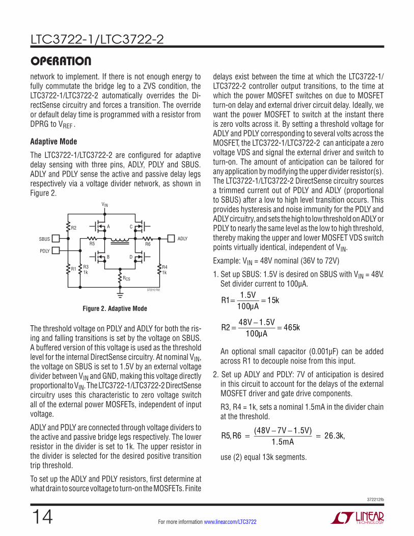
Adaptive Mode
The LTC3722-1/LTC3722-2 are configured for adaptive delay sensing with three pins, ADLY, PDLY and SBUS. ADLY and PDLY sense the active and passive delay legs respectively via a voltage divider network, as shown in Figure 2.
delays exist between the time at which the LTC3722-1/LTC3722-2 controller output transitions, to the time at which the power MOSFET switches on due to MOSFET turn-on delay and external driver circuit delay. Ideally, we want the power MOSFET to switch at the instant there is zero volts across it. By setting a threshold voltage for ADLY and PDLY corresponding to several volts across the MOSFET, the LTC3722-1/LTC3722-2 can anticipate a zero voltage VDS and signal the external driver and switch to turn-on. The amount of anticipation can be tailored for any application by modifying the upper divider resistor(s). The LTC3722-1/LTC3722-2 DirectSense circuitry sources a trimmed current out of PDLY and ADLY (proportional to SBUS) after a low to high level transition occurs. This provides hysteresis and noise immunity for the PDLY and ADLY circuitry, and sets the high to low threshold on ADLY or PDLY to nearly the same level as the low to high threshold, thereby making the upper and lower MOSFET VDS switch points virtually identical, independent of VIN.
Example: VIN = 48V nominal (36V to 72V)
1. Set up SBUS: 1.5V is desired on SBUS with VIN = 48V. Set divider current to 100µA.
R1= 1.5V100µA
= 15k
R2 = 48V − 1.5V100µA
= 465k
An optional small capacitor (0.001µF) can be added across R1 to decouple noise from this input.
2. Set up ADLY and PDLY: 7V of anticipation is desired in this circuit to account for the delays of the external MOSFET driver and gate drive components.
R3, R4 = 1k, sets a nominal 1.5mA in the divider chain at the threshold.
R5,R6 = (48V − 7V − 1.5V)
1.5mA= 26.3k,
use (2) equal 13k segments.
OPERATION
The threshold voltage on PDLY and ADLY for both the ris-ing and falling transitions is set by the voltage on SBUS. A buffered version of this voltage is used as the threshold level for the internal DirectSense circuitry. At nominal VIN, the voltage on SBUS is set to 1.5V by an external voltage divider between VIN and GND, making this voltage directly proportional to VIN. The LTC3722-1/LTC3722-2 DirectSense circuitry uses this characteristic to zero voltage switch all of the external power MOSFETs, independent of input voltage.
ADLY and PDLY are connected through voltage dividers to the active and passive bridge legs respectively. The lower resistor in the divider is set to 1k. The upper resistor in the divider is selected for the desired positive transition trip threshold.
To set up the ADLY and PDLY resistors, first determine at what drain to source voltage to turn-on the MOSFETs. Finite
SBUS ADLY
PDLY
R2
R5 R6
R1 R31k
R41k
RCS
A
B
C
D
VIN
372212 F02
Figure 2. Adaptive Mode

LTC3722-1/LTC3722-2
15372212fb
For more information www.linear.com/LTC3722
Fixed Delay Mode
The LTC3722-1/LTC3722-2 provides the flexibility through the SBUS pin to disable the DirectSense delay circuitry and enable fixed ZVS delays. The level of fixed ZVS delay is proportional to the voltage programmed through the voltage divider on the PDLY and ADLY pins (see Figure 3 for more detail).
Programming Adaptive Delay Time-Out
The LTC3722-1/LTC3722-2 controllers include a feature to program the maximum time delay before a bridge switch turn on command is summoned. This function will come into play if there is not enough energy to commutate a bridge leg to the opposite supply rail, therefore bypass-ing the adaptive delay circuitry. The time delay can be set with an external resistor connected between DPRG and VREF (see Figure 4). The nominal regulated voltage on DPRG is 2V. The external resistor programs a current which flows into DPRG. The delay can be adjusted from approximately 35ns to 300ns, depending on the resistor value. If DPRG is left open, the delay time is approximately 400ns. The amount of delay can also be modulated based on an external current source that feeds current into DPRG. Care must be taken to limit the current fed into DPRG to 350µA or less.
Powering the LTC3722-1/LTC3722-2
The LTC3722-1/LTC3722-2 utilize an integrated VCC shunt regulator to serve the dual purposes of limiting the volt-age applied to VCC as well as signaling that the chip’s bias voltage is sufficient to begin switching operation (under-voltage lockout). With its typical 10.2V turn-on voltage and 4.2V UVLO hysteresis, the LTC3722-1/LTC3722-2 is tolerant of loosely regulated input sources such as an auxiliary transformer winding. The VCC shunt is capable of sinking up to 25mA of externally applied current. The UVLO turn-on and turn-off thresholds are derived from an internally trimmed reference making them extremely accurate. In addition, the LTC3722-1/LTC3722-2 exhibits very low (145µA typ) start-up current that allows the use of 1/8W to 1/4W trickle charge start-up resistors.
The trickle charge resistor should be selected as follows:
RSTART(MAX) = VIN(MIN) − 10.7V
250µA
Adding a small safety margin and choosing standard values yields:
APPLICATION VIN RANGE RSTART
DC/DC 36V TO 72V 100k
Off-Line 85V to 270VRMS 430k
PFC Preregulator 390VDC 1.4M
VCC should be bypassed with a 0.1µF to 1µF multilayer ceramic capacitor to decouple the fast transient currents demanded by the output drivers and a bulk tantalum or electrolytic capacitor to hold up the VCC supply before the bootstrap winding, or an auxiliary regulator circuit takes over.
CHOLDUP = (ICC + IDRIVE ) •tDELAY
3.8V(minimum UVLO hysteresis)
OPERATION
Figure 3. Setup for Fixed ZVS Delays
ADLY
PDLY
VREF
SBUS
372212 F03
R1
R2
R3
Figure 4. Delay Timeout Circuitry
–
+TURN-ON OUTPUT
SBUS
+
–V 2V
VREF
DPRGRDPRG
372212 F04
LTC3722-1/LTC3722-2
16372212fb
For more information www.linear.com/LTC3722
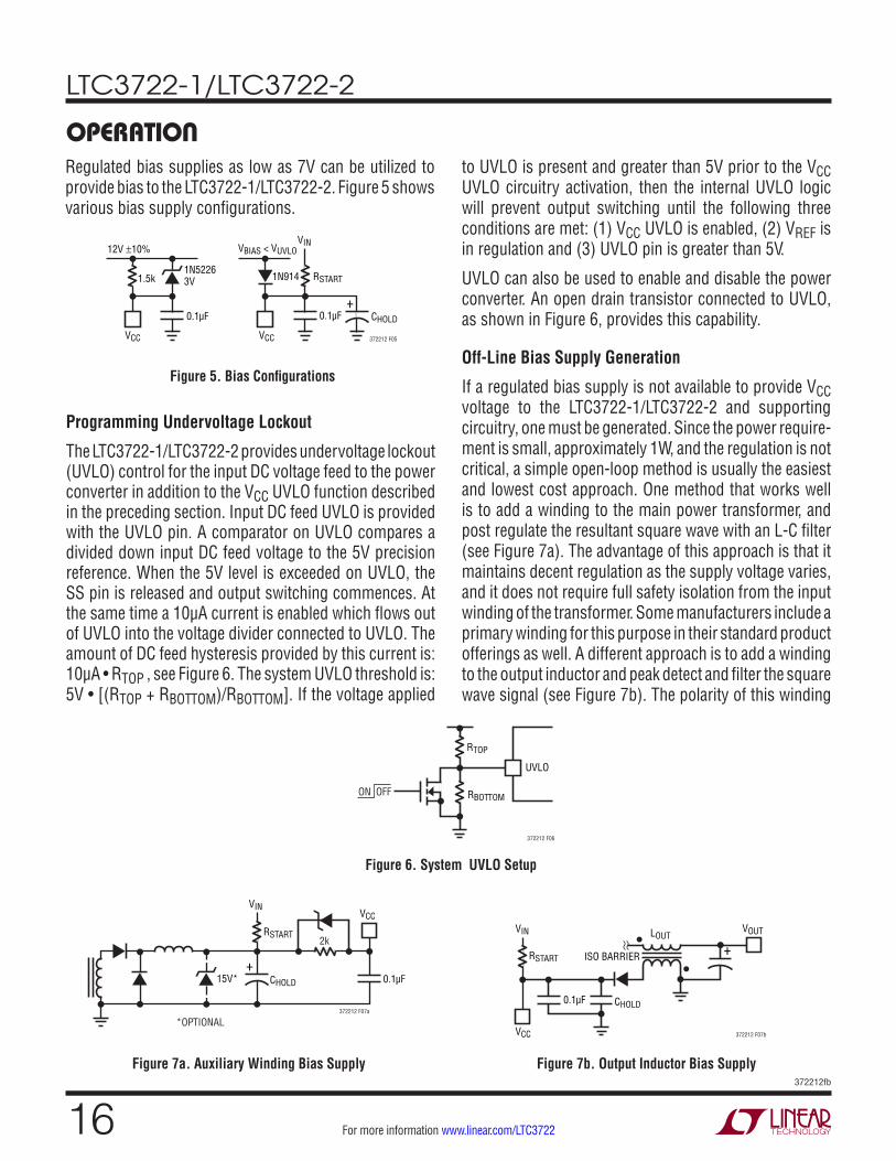
Regulated bias supplies as low as 7V can be utilized to provide bias to the LTC3722-1/LTC3722-2. Figure 5 shows various bias supply configurations.
Programming Undervoltage Lockout
The LTC3722-1/LTC3722-2 provides undervoltage lockout (UVLO) control for the input DC voltage feed to the power converter in addition to the VCC UVLO function described in the preceding section. Input DC feed UVLO is provided with the UVLO pin. A comparator on UVLO compares a divided down input DC feed voltage to the 5V precision reference. When the 5V level is exceeded on UVLO, the SS pin is released and output switching commences. At the same time a 10µA current is enabled which flows out of UVLO into the voltage divider connected to UVLO. The amount of DC feed hysteresis provided by this current is: 10µA • RTOP , see Figure 6. The system UVLO threshold is: 5V • [(RTOP + RBOTTOM)/RBOTTOM]. If the voltage applied
to UVLO is present and greater than 5V prior to the VCC UVLO circuitry activation, then the internal UVLO logic will prevent output switching until the following three conditions are met: (1) VCC UVLO is enabled, (2) VREF is in regulation and (3) UVLO pin is greater than 5V.
UVLO can also be used to enable and disable the power converter. An open drain transistor connected to UVLO, as shown in Figure 6, provides this capability.
Off-Line Bias Supply Generation
If a regulated bias supply is not available to provide VCC voltage to the LTC3722-1/LTC3722-2 and supporting circuitry, one must be generated. Since the power require-ment is small, approximately 1W, and the regulation is not critical, a simple open-loop method is usually the easiest and lowest cost approach. One method that works well is to add a winding to the main power transformer, and post regulate the resultant square wave with an L-C filter (see Figure 7a). The advantage of this approach is that it maintains decent regulation as the supply voltage varies, and it does not require full safety isolation from the input winding of the transformer. Some manufacturers include a primary winding for this purpose in their standard product offerings as well. A different approach is to add a winding to the output inductor and peak detect and filter the square wave signal (see Figure 7b). The polarity of this winding
OPERATION
Figure 5. Bias Configurations
372212 F05
12V ±10%
1.5k
VCC
VIN
VCC
CHOLD
1N52263V
0.1µF 0.1µF
VBIAS < VUVLO
RSTART1N914
+
Figure 7a. Auxiliary Winding Bias Supply
372212 F07a
+
VCCVIN
CHOLD 0.1µF
RSTART2k
15V*
*OPTIONAL372212 F07bVCC
VOUTVIN
CHOLD
RSTART+
0.1µF
LOUT
ISO BARRIER
ON OFF RBOTTOM
RTOP
UVLO
372212 F06
Figure 7b. Output Inductor Bias Supply
Figure 6. System UVLO Setup
LTC3722-1/LTC3722-2
17372212fb
For more information www.linear.com/LTC3722
is designed so that the positive voltage square wave is produced while the output inductor is freewheeling. An advantage of this technique over the previous is that it does not require a separate filter inductor and since the voltage is derived from the well regulated output voltage, it is also well controlled. One disadvantage is that this wind-ing will require the same safety isolation that is required for the main transformer. Another disadvantage is that a much larger VCC filter capacitor is needed, since it does not generate a voltage as the output is first starting up, or during short-circuit conditions.
Programming the LTC3722-1/LTC3722-2 Oscillator
The high accuracy LTC3722-1/LTC3722-2 oscillator circuit provides flexibility to program the switching frequency, slope compensation, and synchronization with minimal external components. The LTC3722-1/LTC3722-2 oscillator circuitry produces a 2.2V peak-to-peak amplitude ramp waveform on CT and a narrow pulse on SYNC that can be used to synchronize other PWM chips. Typical maximum duty cycles of 98.5% are obtained at 300kHz and 96% at 1MHz. A compensating slope current is derived from the oscillator ramp waveform and sourced out of CS.
The desired amount of slope compensation is selected with single external resistor. A capacitor to GND on CT programs the switching frequency. The CT ramp discharge current is internally set to a high value (>10mA). The dedi-cated SYNC I/O pin easily achieves synchronization. The
LTC3722-1/LTC3722-2 can be set up to either synchronize other PWM chips or be synchronized by another chip or external clock source. The 1.8V SYNC threshold allows the LTC3722-1/LTC3722-2 to be synchronized directly from all standard 3V and 5V logic families.
Design Procedure:
1. Choose CT for the desired oscillator frequency. The switching frequency selected must be consistent with the power magnetics and output power level. In general, increasing the switching frequency will decrease the maximum achievable output power, due to limitations of maximum duty cycle imposed by transformer core reset and ZVS. Remember that the tranformer fre- quency is one-half that of the oscillator.
CT = 1
(13.4k • fOSC)
Example: Desired fOSC = 330kHz
CT = 1/(13.4k • fOSC) = 226pF, choose closest standard value of 220pF. A 5% or better tolerance multilayer NPO or X7R ceramic capacitor is recommended for best performance.
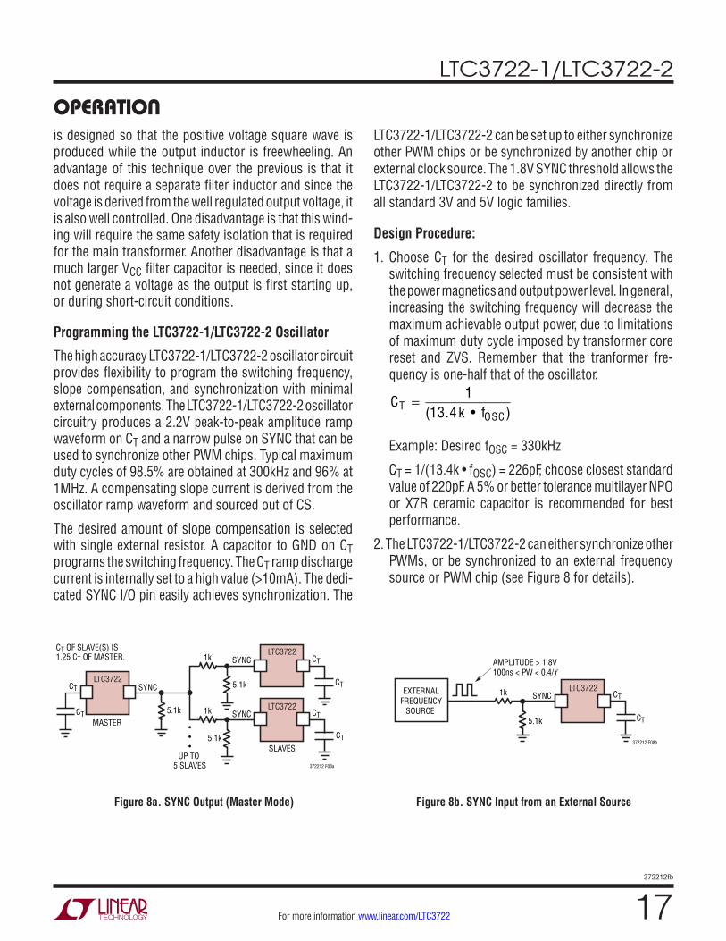
2. The LTC3722-1/LTC3722-2 can either synchronize other PWMs, or be synchronized to an external frequency source or PWM chip (see Figure 8 for details).
OPERATION
Figure 8a. SYNC Output (Master Mode) Figure 8b. SYNC Input from an External Source
LTC3722
LTC3722
LTC3722CT
CT
CT
CT
CT
CT
SYNC
SYNC
SYNC
5.1k
5.1k
5.1k
1k
1k
•••
UP TO 5 SLAVES
SLAVES
MASTER
CT OF SLAVE(S) IS 1.25 CT OF MASTER.
372212 F08a
LTC3722CT
CT
SYNC
5.1k
1k
372212 F08b
EXTERNALFREQUENCY
SOURCE
AMPLITUDE > 1.8V100ns < PW < 0.4/ƒ
LTC3722-1/LTC3722-2
18372212fb
For more information www.linear.com/LTC3722
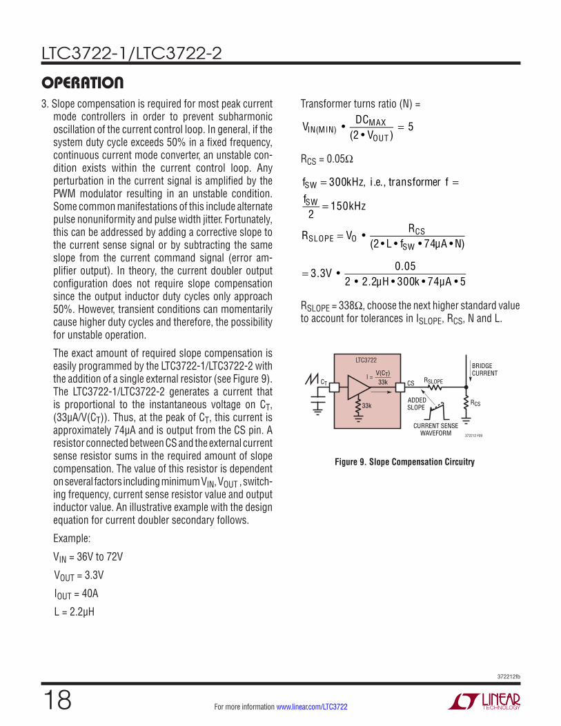
3. Slope compensation is required for most peak current mode controllers in order to prevent subharmonic oscillation of the current control loop. In general, if the system duty cycle exceeds 50% in a fixed frequency, continuous current mode converter, an unstable con-dition exists within the current control loop. Any perturbation in the current signal is amplified by the PWM modulator resulting in an unstable condition. Some common manifestations of this include alternate pulse nonuniformity and pulse width jitter. Fortunately, this can be addressed by adding a corrective slope to the current sense signal or by subtracting the same slope from the current command signal (error am-plifier output). In theory, the current doubler output configuration does not require slope compensation since the output inductor duty cycles only approach 50%. However, transient conditions can momentarily cause higher duty cycles and therefore, the possibility for unstable operation.
The exact amount of required slope compensation is easily programmed by the LTC3722-1/LTC3722-2 with the addition of a single external resistor (see Figure 9). The LTC3722-1/LTC3722-2 generates a current that is proportional to the instantaneous voltage on CT, (33µA/V(CT)). Thus, at the peak of CT, this current is approximately 74µA and is output from the CS pin. A resistor connected between CS and the external current sense resistor sums in the required amount of slope compensation. The value of this resistor is dependent on several factors including minimum VIN, VOUT , switch-ing frequency, current sense resistor value and output inductor value. An illustrative example with the design equation for current doubler secondary follows.
Example:
VIN = 36V to 72V
VOUT = 3.3V
IOUT = 40A
L = 2.2µH
Transformer turns ratio (N) =
VIN(MIN) •
DCMAX
(2 • VOUT )= 5
RCS = 0.05Ω
fSW = 300kHz, i .e., transformer f =fSW
2= 150kHz
RSLOPE = VO •RCS
(2 • L • fSW • 74µA • N)
= 3.3V •0.05
2 • 2.2µH • 300k • 74µA • 5
RSLOPE = 338Ω, choose the next higher standard value to account for tolerances in ISLOPE, RCS, N and L.
OPERATION
Figure 9. Slope Compensation Circuitry
BRIDGECURRENT
CURRENT SENSEWAVEFORM
V(CT)33k
I = CSCT
33kADDEDSLOPE
RSLOPE
RCS
372212 F09
LTC3722

LTC3722-1/LTC3722-2
19372212fb
For more information www.linear.com/LTC3722
Current Sensing and Overcurrent Protection
Current sensing provides feedback for the current mode control loop and protection from overload conditions. The LTC3722-1/LTC3722-2 are compatible with either resis-tive sensing or current transformer methods. Internally connected to the LTC3722-1/LTC3722-2 CS pin are two comparators that provide pulse-by-pulse and overcurrent shutdown functions respectively (see Figure 10).
The pulse-by-pulse comparator has a 300mV nominal threshold. If the 300mV threshold is exceeded, the PWM cycle is terminated. The overcurrent comparator is set approximately 2x higher than the pulse-by-pulse level. If the current signal exceeds this level, the PWM cycle is terminated, the soft-start capacitor is quickly discharged and a soft-start cycle is initiated. If the overcurrent condition persists, the LTC3722-1/LTC3722-2 halts PWM operation and waits for the soft-start capacitor to charge up to ap-proximately 4V before a retry is allowed. The soft-start capacitor is charged by an internal 12µA current source. If the fault condition has not cleared when soft-start reaches 4V, the soft-start pin is again discharged and a new cycle is initiated. This is referred to as hiccup mode operation. In normal operation and under most abnormal conditions, the pulse-by-pulse comparator is fast enough to prevent hiccup mode operation. In severe cases, how-
ever, with high input voltage, very low RDS(ON) MOSFETs and a shorted output, or with saturating magnetics, the overcurrent comparator provides a means of protecting the power converter.
Leading Edge Blanking
The LTC3722-1/LTC3722-2 provides programmable leading edge blanking to prevent nuisance tripping of the current sense circuitry. Leading edge blanking relieves the filter-ing requirements for the CS pin, greatly improving the response to real overcurrent conditions. It also allows the use of a ground referenced current sense resistor or transformer(s), further simplifying the design. With a single 10k to 100k resistor from RLEB to GND, blanking times of approximately 40ns to 320ns are programmed. If not required, connecting RLEB to VREF can disable leading edge blanking. Keep in mind that the use of leading edge blanking will set a minimum linear control range for the phase modulation circuitry.
Resistive Sensing
A resistor connected between input common and the sources of MB and MD is the simplest method of current sensing for the full bridge converter. This is the preferred method for low to moderate power levels. The sense resistor should be chosen such that the maximum rated
OPERATION
Figure 10. Current Sense/Fault Circuitry Detail
+
–
+
–
OVERLOADCURRENT LIMIT
300mV
650mV
φMOD
UVLOENABLE
UVLOENABLE
R
S Q
R
S Q
Q
QS
Q PWMLOGIC
H = SHUTDOWN OUTPUTS
CS
RCS
+
–
+
–
CSS
SS
0.4V
4.1V 12µA
372212 F10
PULSE BY PULSECURRENT LIMIT
PWMLATCH
BLANK

LTC3722-1/LTC3722-2
20372212fb
For more information www.linear.com/LTC3722
output current for the converter can be delivered at the lowest expected VIN. Use the following formula to calculate the optimal value for RCS. IP equation valid for current doubler secondary.
LTC3722-1:
RCS =300mV – (82.5µA • RSLOPE )
IP(PEAK)
IP(PEAK) =IO(MAX)
2 • N • EFF+
VIN(MAX) • DMIN
LMAG • f CLK • 2+
VO(1– DMIN)LOUT • f CLK • N
where : N = Transformer turns ratio = NP
NS
LTC3722-2:
RCS = 300mV
IP(PEAK)
Current Transformer Sensing
A current sense transformer can be used in lieu of resistive sensing with the LTC3722-1/LTC3722-2. Current sense transformers are available in many styles from several manufacturers. A typical sense transformer for this ap-plication will use a 1:50 turns ratio (N), so that the sense resistor value is N times larger, and the secondary current N times smaller than in the resistive sense case. Therefore, the sense resistor power loss is about N times less with the transformer method, neglecting the transformers core and copper losses. The disadvantages of this approach include, higher cost and complexity, lower accuracy, core reset/maximum duty cycle limitations and lower speed. Nevertheless, for very high power applications, this method is preferred. The sense transformer primary is placed in the same location as the ground referenced sense resistor, or between the upper MOSFET drains in the (MA, MC) and VIN.
The advantage of the high side location is a greater im-munity to leading edge noise spikes, since gate charge current and reflected rectifier recovery current are largely eliminated. Figure 11 illustrates a typical current sense transformer based sensing scheme. RS in this case is calculated the same as in the resistive case, only its value is increased by the sense transformer turns ratio. At high duty cycles, it may become difficult or impossible to re-set the current transformer. This is because the required transformer reset voltage increases as the available time for reset decreases to equalize the (volt • seconds) applied. The interwinding capacitance and secondary inductance of the current sense transformer form a resonant circuit that limits the dV/dT on the secondary of the CS transformer. This, in turn, limits the maximum achievable duty cycle for the CS transformer. Attempts to operate beyond this limit will cause the transformer core to “walk” and eventually saturate, opening up the current feedback loop.
Common methods to address this limitation include:
1. Reducing the maximum duty cycle by lowering the power transformer turns ratio.
2. Reducing the switching frequency of the converter.
3. Employ external active reset circuitry.
4. Using two CS transformers summed together.
5. Choose a CS transformer optimized for high frequency applications.
OPERATION
Figure 11. Current Transformer Sense Circuitry
OPTIONALFILTERING
N:1
MBSOURCE
MDSOURCE
CURRENTTRANSFORMER
RSLOPERAMP
CS
RS
372212 F11

LTC3722-1/LTC3722-2
21372212fb
For more information www.linear.com/LTC3722
Phase Modulator (LTC3722-1)
The LTC3722-1 phase modulation control circuitry is comprised of the phase modulation comparator and logic, the error amplifier, and the soft-start amplifier (see Figure 12). Together, these elements develop the required phase overlap (duty cycle) required to keep the output voltage in regulation. In isolated applications, the sensed output voltage error signal is fed back to COMP across the input to output isolation boundary by an optical coupler and shunt reference/error amplifier (LT®1431) combina-tion. The FB pin is connected to GND, forcing COMP high. The collector of the optoisolator is connected to COMP directly. The voltage COMP is internally attenuated by the LTC3722-1. The attenuated COMP voltage provides one input to the phase modulation comparator. This is the current command. The other input to the phase modula-tion comparator is the RAMP voltage, level shifted by approximately 650mV. This is the current loop feedback. During every switching cycle, alternate diagonal switches (MA-MD or MB-MC) conduct and cause current in an output inductor to increase. This current is seen on the primary of the power transformer divided by the turns ratio. Since
the current sense resistor is connected between GND and the two bottom bridge transistors, a voltage proportional to the output inductor current will be seen across RSENSE. The high side of RSENSE is also connected to CS, usually through a small resistor (RSLOPE). When the voltage on CS exceeds either (COMP/4.3) –650mV, or 300mV, the overlap conduction period will terminate. During normal operation, the attenuated COMP voltage will determine the CS trip point. During start-up, or slewing conditions following a large load step, the 300mV CS threshold will terminate the cycle, as COMP will be driven high, such that the attenuated version exceeds the 300mV threshold. In extreme conditions, the 650mV threshold on CS will be exceeded, invoking a soft-start/restart cycle.
Selecting the Power Stage Components
Perhaps the most critical part of the overall design of the converter is selecting the power MOSFETs, transformer, inductors and filter capacitors. Tremendous gains in ef-ficiency, transient performance and overall operation can be obtained as long as a few simple guidelines are followed with the phase-shifted full bridge topology.
OPERATION
Figure 12. Phase Modulation Circuitry (LTC3722-1)
650mV12µA
372212 F12
R
S Q
R
SQ
+
–
+
–
+
–
+
–
Q
Q
C
B
D
ACLK
CLK
CLK
1.2V
VREF
SOFT-STARTAMPLIFIER
IDEAL
ERRORAMPLIFIER
TOGGLEF/F
PHASEMODULATION
LOGIC
PHASEMODULATIONCOMPARATOR
FROMCURRENTLIMITCOMPARATOR
BLANKING
FB
COMP
SS
RLEB
CS
14.9k
50k

LTC3722-1/LTC3722-2
22372212fb
For more information www.linear.com/LTC3722
Power Transformer
Switching frequency, core material characteristics, series resistance and input/output voltages all play an important role in transformer selection. Close attention also needs to be paid to leakage and magnetizing inductances as they play an important role in how well the converter will achieve ZVS. Planar magnetics are very well suited to these applications because of their excellent control of these parameters.
Turns Ratio
The required turns ratio for a current doubler secondary is given below. Depending on the magnetics selected, this value may need to be reduced slightly.
Turns ratio formula:
N =
VIN(MIN) •DMAX
2 • VOUT
where:
VIN(MIN) = Minimum VIN for operation
DMAX = Maximum duty cycle of controller (DCMAX)
Output Capacitors
Output capacitor selection has a dramatic impact on ripple voltage, dynamic response to transients and stability. Capacitor ESR along with output inductor ripple current will determine the peak-to-peak voltage ripple on the out-put. The current doubler configuration is advantageous because it has inherent ripple current reduction. The dual output inductors deliver current to the output capacitor 180 degrees out-of-phase, in effect, partially canceling each other’s ripple current. This reduction is maximized at high duty cycle and decreases as the duty cycle reduces. This means that a current doubler converter requires less output capacitance for the same performance as a conventional converter. By determining the minimum duty cycle for the converter, worse-case VOUT ripple can be derived by the following formula:
VORIPPLE = IRIPPLE •ESR = VO •ESR
LO • 2 • f SW(1– D)(1– 2D)
OPERATIONwhere:
D = minimum duty cycle
fSW = oscillator frequency
LO = output inductance
ESR = output capacitor series resistance
The amount of bulk capacitance required is usually system dependent, but has some relationship to output inductance value, switching frequency, load power and dynamic load characteristics. Polymer electrolytic capacitors are the preferred choice for their combination of low ESR, small size and high reliability. For less demanding applications, or those not constrained by size, aluminum electrolytic capacitors are commonly applied. Most DC/DC convert-ers in the 100kHz to 300kHz range use 20µF to 25µF of bulk capacitance per watt of output power. Converters switching at higher frequencies can usually use less bulk capacitance. In systems where dynamic response is critical, additional high frequency capacitors, such as ceramics, can substantially reduce voltage transients.
Power MOSFETs
The full bridge power MOSFETs should be selected for their RDS(ON) and BVDSS ratings. Select the lowest BVDSS rated MOSFET available for a given input voltage range leaving at least a 20% voltage margin. Conduction losses are directly proportional to RDS(ON). Since the full bridge has two MOSFETs in the power path most of the time, conduction losses are approximately equal to:
2 • RDS(ON) • I2, where I = IO
2N
Switching losses in the MOSFETs are dominated by the power required to charge their gates, and turn-on and turn-off losses. At higher power levels, gate charge power is seldom a significant contributor to efficiency loss. ZVS operation virtually eliminates turn-on losses. Turn-off losses are reduced by the use of an external drain to source snubber capacitor and/or a very low resistance turn-off driver. If synchronous rectifier MOSFETs are used on the secondary, the same general guidelines apply. Keep in mind, however, that the BVDSS rating needed for these can be greater than VIN(MAX)/N, depending on how well the

LTC3722-1/LTC3722-2
23372212fb
For more information www.linear.com/LTC3722
OPERATIONsecondary is snubbed. Without snubbing, the secondary voltage can ring to levels far beyond what is expected due to the resonant tank circuit formed between the secondary leakage inductance and the COSS (output capacitance) of the synchronous rectifier MOSFETs.
Switching Frequency Selection
Unless constrained by other system requirements, the power converter’s switching frequency is usually set as high as possible while staying within the desired efficiency target. The benefits of higher switching frequencies are many including smaller size, weight and reduced bulk capacitance. In the full bridge phase-shift converter, these principles are generally the same with the added complica-tion of maintaining zero voltage transitions, and therefore, higher efficiency. ZVS is achieved in a finite time during the switching cycle. During the ZVS time, power is not delivered to the output; the act of ZVS reduces the maxi-mum available duty cycle. This reduction is proportional to maximum output power since the parasitic capacitive element (MOSFETs) that increase ZVS time get larger as power levels increase. This implies an inverse relationship between output power level and switching frequency. Table 1 displays recommended maximum switching frequency vs power level for a 30V/75V in to 3.3V/5V out converter. Higher switching frequencies can be used if the input voltage range is limited, the output voltage is lower and/or lower efficiency can be tolerated.
Table 1. Switching Frequency vs Power Level<50W 600kHz
<100W 450kHz
<200W 300kHz
<500W 200kHz
<1kW 150kHz
<2kW 100kHz
Closing the Feedback Loop
Closing the feedback loop with the full bridge converter involves identifying where the power stage and other system poles/zeroes are located and then designing a com-pensation network around the converters error amplifier to shape the frequency response to insure adequate phase
margin and transient response. Additional modifications will sometimes be required in order to deal with parasitic elements within the converter that can alter the feedback response. The compensation network will vary depending on the load current range and the type of output capacitors used. In isolated applications, the compensation network is generally located on the secondary side of the power supply, around the error amplifier of the opto-coupler driver, usually an LT1431 or equivalent. In nonisolated systems, the compensation network is located around the LTC3722-1/LTC3722-2’s error amplifier.
In current mode control, the dominant system pole is determined by the load resistance (VO/ IO) and the output capacitor 1/(2π • RO • CO). The output capacitors ESR 1/(2π • ESR • CO) introduces a zero. Excellent DC line and load regulation can be obtained if there is high loop gain at DC. This requires an integrator type of compensator around the error amplifier. A procedure is provided for deriving the required compensation components. More complex types of compensation networks can be used to obtain higher bandwidth if necessary.
Step 1. Calculate location of minimum and maximum output pole:
FP1(MIN) = 1(2π •RO(MAX) • CO)
FP1(MAX) = 1(2π •RO(MIN) • CO)
Step 2. Calculate ESR zero location:
FZ1 = 1
(2π •RESR • CO)
Step 3. Calculate the feedback divider gain:
RB
(RB + RT )or
VREF
VOUT
If polymer electrolytic output capacitors are used, the ESR zero can be employed in the overall loop compensation and optimum bandwidth can be achieved. If aluminum electrolytics are used, the loop will need to be rolled off prior to the ESR zero frequency, making the loop response slower. A linearized SPICE macromodel of the control
LTC3722-1/LTC3722-2
24372212fb
For more information www.linear.com/LTC3722
loop is very helpful tool to quickly evaluate the frequency response of various compensation networks.
Polymer Electrolytic (see Figure 13) 1/(2πCCRI) sets a low frequency pole. 1/(2πCCRF) sets the low frequency zero. The zero frequency should coincide with the worst-case lowest output pole frequency. The pole frequency and mid frequency gain (RF/RI) should be set such so that the loop crosses over zero dB with a –1 slope at a frequency lower than (fSW/8). Use a bode plot to graphi-cally display the frequency response. An optional higher frequency pole set by CP2 and Rf is used to attenuate switching frequency noise.
Aluminum Electrolytic (see Figure 13) the goal of this compensator will be to cross over the output minimum pole frequency. Set a low frequency pole with CC and RIN at a frequency that will cross over the loop at the output pole minimum F, place the zero formed by CC and Rf at the output pole F.
improve transient response, particularly overshoot, and improve ZVS ability at light loads.
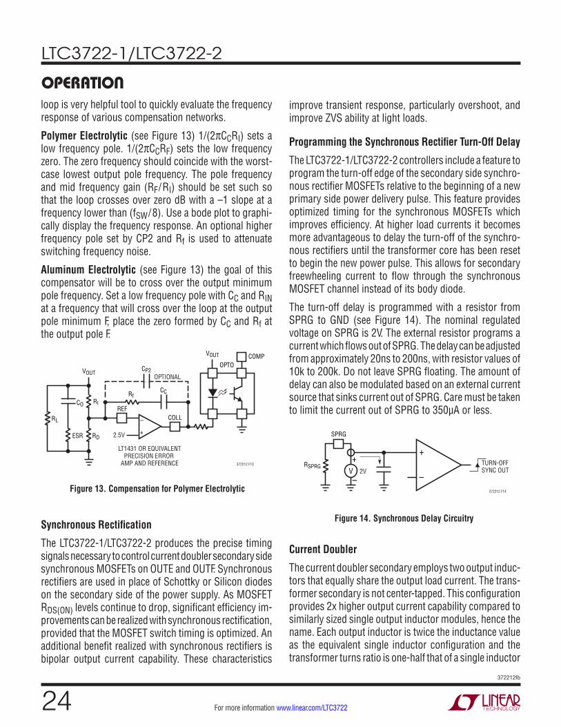
Programming the Synchronous Rectifier Turn-Off Delay
The LTC3722-1/LTC3722-2 controllers include a feature to program the turn-off edge of the secondary side synchro-nous rectifier MOSFETs relative to the beginning of a new primary side power delivery pulse. This feature provides optimized timing for the synchronous MOSFETs which improves efficiency. At higher load currents it becomes more advantageous to delay the turn-off of the synchro-nous rectifiers until the transformer core has been reset to begin the new power pulse. This allows for secondary freewheeling current to flow through the synchronous MOSFET channel instead of its body diode.
The turn-off delay is programmed with a resistor from SPRG to GND (see Figure 14). The nominal regulated voltage on SPRG is 2V. The external resistor programs a current which flows out of SPRG. The delay can be adjusted from approximately 20ns to 200ns, with resistor values of 10k to 200k. Do not leave SPRG floating. The amount of delay can also be modulated based on an external current source that sinks current out of SPRG. Care must be taken to limit the current out of SPRG to 350µA or less.
Figure 14. Synchronous Delay Circuitry
Figure 13. Compensation for Polymer Electrolytic
+
–
2.5V
Rf
RL
RDESR
REFRI
CC
CO
CP2VOUT
COLL
COMPOPTO
VOUT
LT1431 OR EQUIVALENTPRECISION ERROR
AMP AND REFERENCE
OPTIONAL
372212 F13
–
+TURN-OFF SYNC OUT
372212 F14
+
–V 2V
SPRG
RSPRG
Synchronous Rectification
The LTC3722-1/LTC3722-2 produces the precise timing signals necessary to control current doubler secondary side synchronous MOSFETs on OUTE and OUTF. Synchronous rectifiers are used in place of Schottky or Silicon diodes on the secondary side of the power supply. As MOSFET RDS(ON) levels continue to drop, significant efficiency im-provements can be realized with synchronous rectification, provided that the MOSFET switch timing is optimized. An additional benefit realized with synchronous rectifiers is bipolar output current capability. These characteristics
Current Doubler
The current doubler secondary employs two output induc-tors that equally share the output load current. The trans-former secondary is not center-tapped. This configuration provides 2x higher output current capability compared to similarly sized single output inductor modules, hence the name. Each output inductor is twice the inductance value as the equivalent single inductor configuration and the transformer turns ratio is one-half that of a single inductor
OPERATION
LTC3722-1/LTC3722-2
25372212fb
For more information www.linear.com/LTC3722
secondary. The drive to the inductors is 180 degrees out-of-phase which provides partial ripple current cancellation in the output capacitor(s). Reduced capacitor ripple current lowers output voltage ripple and enhances the capacitors’s reliability. The amount of ripple cancellation is related to duty cycle (see Figure 15). Although the current doubler requires an additional inductor, the inductor core volume is proportional to LI2, thus the size penalty is small. The transformer construction is simplified without a center-tap winding and the turns ratio is reduced by one-half compared to a conventional full wave rectifier configuration.
Synchronous rectification of the current doubler second-ary requires two ground referenced N-channel MOSFETs. The timing of the LTC3722-1/LTC3722-2 drive signals is shown in the Timing Diagram.
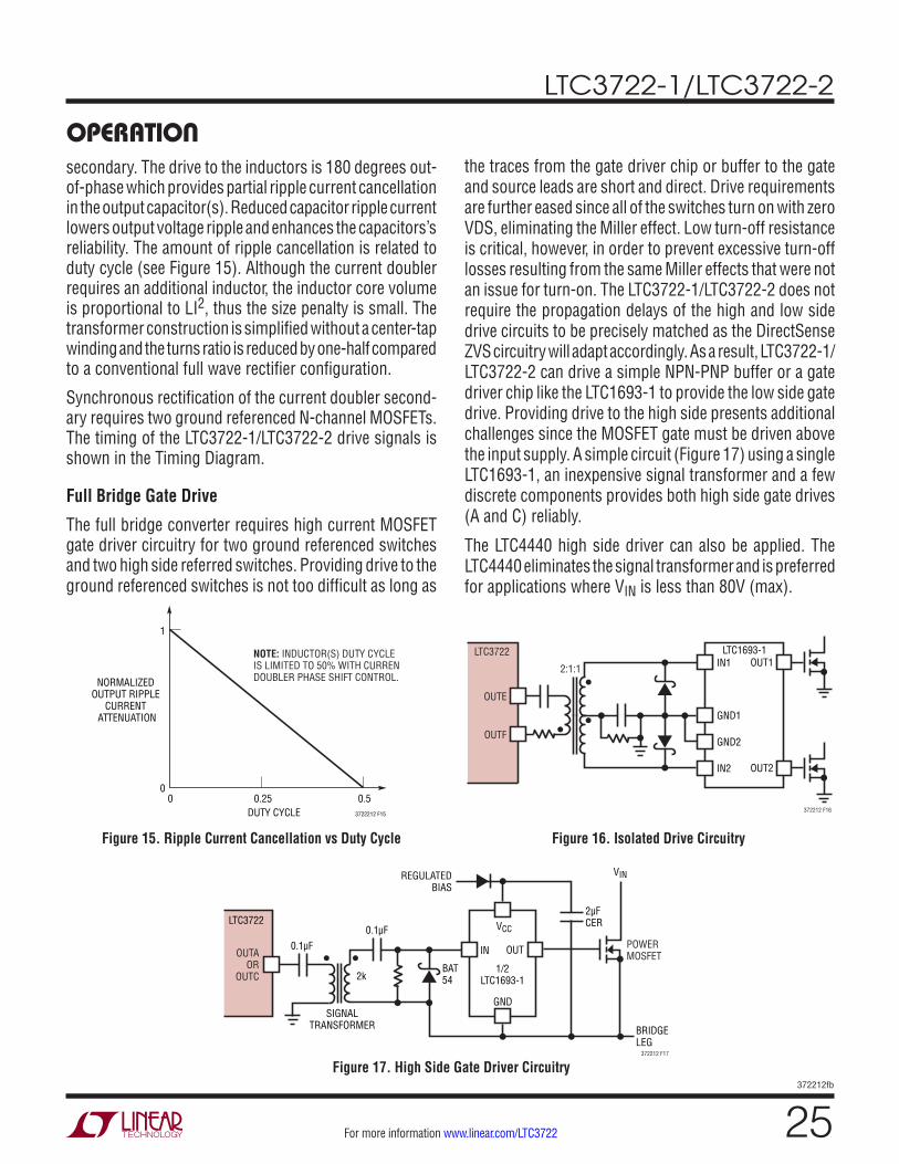
Full Bridge Gate Drive
The full bridge converter requires high current MOSFET gate driver circuitry for two ground referenced switches and two high side referred switches. Providing drive to the ground referenced switches is not too difficult as long as
the traces from the gate driver chip or buffer to the gate and source leads are short and direct. Drive requirements are further eased since all of the switches turn on with zero VDS, eliminating the Miller effect. Low turn-off resistance is critical, however, in order to prevent excessive turn-off losses resulting from the same Miller effects that were not an issue for turn-on. The LTC3722-1/LTC3722-2 does not require the propagation delays of the high and low side drive circuits to be precisely matched as the DirectSense ZVS circuitry will adapt accordingly. As a result, LTC3722-1/LTC3722-2 can drive a simple NPN-PNP buffer or a gate driver chip like the LTC1693-1 to provide the low side gate drive. Providing drive to the high side presents additional challenges since the MOSFET gate must be driven above the input supply. A simple circuit (Figure 17) using a single LTC1693-1, an inexpensive signal transformer and a few discrete components provides both high side gate drives (A and C) reliably.
The LTC4440 high side driver can also be applied. The LTC4440 eliminates the signal transformer and is preferred for applications where VIN is less than 80V (max).
Figure 15. Ripple Current Cancellation vs Duty Cycle
1
00 0.25 0.5
DUTY CYCLE
NORMALIZED OUTPUT RIPPLE
CURRENT ATTENUATION
3722212 F15
NOTE: INDUCTOR(S) DUTY CYCLE IS LIMITED TO 50% WITH CURRENT DOUBLER PHASE SHIFT CONTROL.
Figure 17. High Side Gate Driver Circuitry
Figure 16. Isolated Drive Circuitry
IN1 OUT1
IN2 OUT2
2:1:1
OUTE
OUTF
LTC3722
GND1
GND2
LTC1693-1
372212 F16
IN OUTOUTAOR
OUTC
GND
1/2LTC1693-1
372212 F17
VCC0.1µF
2µFCER
0.1µF
SIGNALTRANSFORMER
2kBAT54
BRIDGELEG
REGULATEDBIAS
POWERMOSFET
VIN
LTC3722
OPERATION

LTC3722-1/LTC3722-2
26372212fb
For more information www.linear.com/LTC3722
PACKAGE DESCRIPTION
.337 – .344*(8.560 – 8.738)
GN24 REV B 0212
1 2 3 4 5 6 7 8 9 10 11 12
.229 – .244(5.817 – 6.198)
.150 – .157**(3.810 – 3.988)
161718192021222324 15 1413
.016 – .050(0.406 – 1.270)
.015 ±.004(0.38 ±0.10)
× 45°
0° – 8° TYP.0075 – .0098(0.19 – 0.25)
.0532 – .0688(1.35 – 1.75)
.008 – .012(0.203 – 0.305)
TYP
.004 – .0098(0.102 – 0.249)
.0250(0.635)
BSC
.033(0.838)
REF
.254 MIN
RECOMMENDED SOLDER PAD LAYOUT
.150 – .165
.0250 BSC.0165 ±.0015
.045 ±.005
* DIMENSION DOES NOT INCLUDE MOLD FLASH. MOLD FLASH SHALL NOT EXCEED 0.006" (0.152mm) PER SIDE** DIMENSION DOES NOT INCLUDE INTERLEAD FLASH. INTERLEAD FLASH SHALL NOT EXCEED 0.010" (0.254mm) PER SIDE
INCHES(MILLIMETERS)
NOTE:1. CONTROLLING DIMENSION: INCHES
2. DIMENSIONS ARE IN
3. DRAWING NOT TO SCALE4. PIN 1 CAN BE BEVEL EDGE OR A DIMPLE
GN Package24-Lead Plastic SSOP (Narrow .150 Inch)
(Reference LTC DWG # 05-08-1641 Rev B)
LTC3722-1/LTC3722-2
27372212fb
For more information www.linear.com/LTC3722
Information furnished by Linear Technology Corporation is believed to be accurate and reliable. However, no responsibility is assumed for its use. Linear Technology Corporation makes no representa-tion that the interconnection of its circuits as described herein will not infringe on existing patent rights.
REVISION HISTORYREV DATE DESCRIPTION PAGE NUMBER
A 03/10 I-grade parts added. Reflected throughout the data sheet. 1 to 28
B 02/13 H-grade part added. Reflected throughout the data sheet. 1 to 28

LTC3722-1/LTC3722-2
28372212fb
For more information www.linear.com/LTC3722 LINEAR TECHNOLOGY CORPORATION 2009
LT 0213 REV B • PRINTED IN USALinear Technology Corporation1630 McCarthy Blvd., Milpitas, CA 95035-7417(408) 432-1900 FAX: (408) 434-0507 www.linear.com/LTC3722
PART NUMBER DESCRIPTION COMMENTS
LTC3723-1/LTC3723-2 Synchronous Push-Pull and Full-Bridge Controllers High Efficiency with On-Chip MOSFET Drivers
LTC3721-1 Non-Synchronous Push-Pull and Full-Bridge Controller Minimizes External Components, On-Chip MOSFET Drivers
LTC3765/LTC3766 Isolated Synchronous Forward Controller Chip Set Ideal for 24V or 48V Input Applications
LT1952/LT1952-1 Isolated Synchronous Forward Controllers Ideal for 24V or 48V Input Applications
LTC3901 Secondary-Side Synchronous Driver for Full-Bridge and Push-Pull Converters
Programmable Timeout, Reverse Inductor Current Sense
LTC4440 High Voltage High Side MOSFET Driver 100V, 2.4A Pull-Up, 1.6Ω Pull-Down, SOT-23 and MSOP-8 Packages
RELATED PARTS
TYPICAL APPLICATION
1k
16
1
ADLY
20k
4.99k
150Ω PDLY OUTB OUTD
VREF DPRG NC SYNC SPRGCT RLEB FB GND PGND SS
CS
11
14 1 24 13 5 6 23 22 7 4
3
2 8
9 2010
18
12
17
OUTF OUTE
15 16
1
8
4
5
150k
5VREF
SBUS
VCC
UVLO
0.47µF
20k1/4W
12VVIN
220pF
1µF
220pF30.1k
182k
COMP
LTC3722-1
B D
Q2
4 2
3
8
1 6
D3
D5
D412V
7
Q4
12V
D
–VOUT
–VOUT
–VOUT
ISNS1.10k
0.02Ω1.5W
0.02Ω1.5W
13k1/2WD1
D6
372212 TA02
+VOUT
Si7852DP×4
Si7852DP×2
Q1
Q3
12V
BSi7852DP×2
Si7852DP×2
Si7852DP×4
+VOUT
12V35A
+VOUT
C1, C2180µF16V×2
0.47µF100V
12V100Ω
D93.3V
L41mH
L2150nH
L1, 1.3µHVIN
36V TO 72V
+VIN
–VIN
D7
1
6
T25:5(105µH):1:1
T15:5(105µH):1:1
7
82
4
2
4
10
11
7
8
10
11
22Ω
0.1µF
T31(1.5mH):0.5
OUTA
21A
OUTC
19C
C368µF20V
0.22µF
D8
1
1
76
5
7
8
6 5
2
3 42
750Ω
200k330Ω
MOC207
5.1k
220pF
10k
33k8.25k D11
100k180pF
2.2nF
330pF
22nF
68nF
C42.2nF250V
ISNS 5VREF
0.047µF
220pF
D125.1V
V+ COMP RTOP
GNDF GNDS RMID
COLL
CSE+6
CSE–5
ME2
8 4 10 13
330pF
1µF
1µF7
4.02k
2.15k
ME23
SYCN
REF
820pF200V
15Ω1.5W
1µF
LT1431
VCC
GND GND TS
INTG
C BOOST
2.7k9.53k 10k
2.49k
–VOUT
470Ω1/4W
4.64k1/4W
100Ω
0.47µF, 100V = TDK C3216X7R2A474M1µF, 100V = TDK C4532X7R2A105MC1, C2: SANYO 16SP180MC3: AVX TPSE686M020R0150C4: MuRata DE2E3KH222MB3BD1, D4, D5, D6: MURS120T3D2, D3, D7, D8: BAS21D9: MMBZ5226BD10: MMBZ5240BD11: BAT54D12: MMBZ5231BL1: SUMIDA CDEP105-1R3MC-50L2: PULSE PA0651L3: PA1294.910L4: COILCRAFT DO1608C-105Q1, Q2: ZETEX FMMT619Q3, Q4: ZETEX FMMT718T1, T2: PULSE PA0526T3: PULSE PA0785
•
VHIGHL3
0.85µH
••
•
••
0.47µF100V
4 2
3
8
16
D212V
7Si7852DP×2
0.22µF
VCC
GND GND TS
IN TGABOOST
LTC4440EMS8E LTC4440EMS8E
1µF100V
1µF100V×4
•+
VHIGH
•
+
51Ω2W
51Ω, 2W
0.47µF100V
CSF+
LTC3901EGN
GND PGND GND2 PGND2 TIMER
PVCC
11CSF–
12MF
14
4.02k
2.15k
MF2 VCC
15
4.64k1/4W
30.1k 100Ω
D1010V
+VOUT
MMBT3904
1M
MMBT3904
LTC3722/LTC4440 420W, 36V-72V Input to 12V/35A Isolated Full Bridge Supply
Top Related