


Languages
Pages
Legal


Radiation Detectors and Signal Processing - IV. Signal Processing Helmuth SpielerOct. 8 – Oct. 12, 2001; Univ. Heidelberg LBNL
1
IV. Signal Processing
1. Continuous Signals 3
2. Pulsed Signals 7
Simple Example: CR-RC Shaping 9
Pulse Shaping and Signal-to-Noise Ratio 10
Ballistic Deficit 16
3. Evaluation of Equivalent Noise Charge 17
Analytical Analysis of a Detector Front-End 19
Equivalent Model for Noise Analysis 20
Determination of Equivalent Noise Charge 26
CR-RC Shapers with Multiple Integrators 30
Examples 32
4. Noise Analysis in the Time Domain 42
Quantitative Analysis of Noise in the Time Domain 51
Correlated Double Sampling 52
5. Detector Noise Summary 62
6. Rate of Noise Pulses in Threshold DiscriminatorSystems 67
7. Some Other Aspects of Pulse Shaping
Baseline Restoration 74
Pole-Zero Cancellation 76
Bipolar vs. Unipolar Shaping 77
Pulse Pile-Up and Pile-Up Rejection 78
Delay Line Clipping 82
8. Timing Measurements 84

Radiation Detectors and Signal Processing - IV. Signal Processing Helmuth SpielerOct. 8 – Oct. 12, 2001; Univ. Heidelberg LBNL
2
9. Digitization of Pulse Height and Time - Analog-to-Digital Conversion 102
A/D Parameters 103
A/D Techniques 113
Time Digitizers 118
10. Digital Signal Processing 120

Radiation Detectors and Signal Processing - IV. Signal Processing Helmuth SpielerOct. 8 – Oct. 12, 2001; Univ. Heidelberg LBNL
3
IV. Signal Processing
1. Continuous Signals
Assume a sinusoidal signal with a frequency of 1 kHz and anamplitude of 1 µV.
If the amplifier has ∆ = 1 MHzf bandwidth and an equivalent input
noise of = 1 nV/ Hzne , the total noise level
πµ= ∆ = ∆ = 1.3 V
2n n n nv e f e f
and the signal-to-noise ratio is 0.8.
The bandwidth of 1 MHz is much greater than needed, as the signalis at 1 kHz, so we can add a simple RC low-pass filter with a cutofffrequency of 2 kHz. Then the total noise level
π= ∆ = ∆ = 56 nV
2n n n nv e f e f
and the signal-to-noise ratio is 18.
log f
log f
Signal
Noise

Radiation Detectors and Signal Processing - IV. Signal Processing Helmuth SpielerOct. 8 – Oct. 12, 2001; Univ. Heidelberg LBNL
4
Since the signal is at a discrete frequency, one can also limit thelower cut-off frequency, i.e. use a narrow bandpass filter centered onthe signal frequency.
For example, if the noise bandwidth is reduced to 100 Hz, the signal-to-noise ratio becomes 100.
How small a bandwidth can one use?
The bandwidth affects the settling time, i.e. the time needed for thesystem to respond to changes in signal amplitude.
Note that a signal of constant amplitude and frequency carries noinformation besides its presence. Any change in transmittedinformation requires either a change in amplitude, phase orfrequency.
Recall from the discussion of the simple amplifier that a bandwidthlimit corresponds to a response time
Frequency Domain Time Domain
input output
log f
)1( /τto eVV −−=
log AV
R1
L Colog ω

Radiation Detectors and Signal Processing - IV. Signal Processing Helmuth SpielerOct. 8 – Oct. 12, 2001; Univ. Heidelberg LBNL
5
The time constant τ corresponds to the upper cutoff frequency
This also applied to a bandpass filter. For example, consider a simplebandpass filter consisting of a series LC resonant circuit. The circuitbandwidth is depends on the dissipative loss in the circuit, i.e. theequivalent series resistance.
The bandwidthω
ω∆ = 0
Qwhere
ω= 0LQR
To a good approximation the settling time
τω
=∆
1/2
Half the bandwidth enters, since the bandwidth is measured as thefull width of the resonance curve, rather then the difference relative tothe center frequency.
uf 21
πτ =
R
v iS i
LC

Radiation Detectors and Signal Processing - IV. Signal Processing Helmuth SpielerOct. 8 – Oct. 12, 2001; Univ. Heidelberg LBNL
6
and the time dependenceτ−= − /(1 )t
oI I e
The figure below shows a numerical simulation of the response whena sinusoidal signal of ω = 710 radians is abruptly switched on andpassed through an LC circuit with a bandwidth of 2 kHz(i.e the dark area is formed by many cycles of the sinusoidal signal).
The signal attains 99% of its peak value after 4.6τ . For a bandwidth∆f = 2 kHz, ∆ω = 4π ⋅103 radians and the settling time τ = 160 µs.
Correspondingly, for the example used above a possible bandwidth∆f = 20 Hz for which the settling time is 16 ms.
⇒⇒ The allowable bandwidth is determined by therate of change of the signal
-1.0
-0.8
-0.6
-0.4
-0.2
0.0
0.2
0.4
0.6
0.8
1.0
0.0E+00 1.0E-04 2.0E-04 3.0E-04 4.0E-04 5.0E-04
TIME [s]
RE
LATI
VE
AM
PLI
TUD
E

Radiation Detectors and Signal Processing - IV. Signal Processing Helmuth SpielerOct. 8 – Oct. 12, 2001; Univ. Heidelberg LBNL
7
2. Pulsed Signals
Two conflicting objectives:
1. Improve Signal-to-Noise Ratio S/N
Restrict bandwidth to match measurement time
⇒⇒ Increase pulse width
Typically, the pulse shaper transforms a narrow detector current pulse to
a broader pulse(to reduce electronic noise),
with a gradually rounded maximum at the peaking time TP
(to facilitate measurement of the amplitude)
Detector Pulse Shaper Output
⇒⇒
If the shape of the pulse does not change with signal level,the peak amplitude is also a measure of the energy, so oneoften speaks of pulse-height measurements or pulse heightanalysis. The pulse height spectrum is the energy spectrum.

Radiation Detectors and Signal Processing - IV. Signal Processing Helmuth SpielerOct. 8 – Oct. 12, 2001; Univ. Heidelberg LBNL
8
2. Improve Pulse Pair Resolution
⇒⇒ Decrease pulse width
Pulse pile-updistorts amplitudemeasurement
Reducing pulseshaping time to1/3 eliminatespile-up.
Necessary to find balance between these conflictingrequirements. Sometimes minimum noise is crucial,sometimes rate capability is paramount.
Usually, many considerations combined lead to a“non-textbook” compromise.
• “Optimum shaping” depends on the application!
• Shapers need not be complicated –Every amplifier is a pulse shaper!
TIMEA
MP
LITU
DE
TIME
AM
PLI
TUD
E

Radiation Detectors and Signal Processing - IV. Signal Processing Helmuth SpielerOct. 8 – Oct. 12, 2001; Univ. Heidelberg LBNL
9
Simple Example: CR-RC Shaping
Preamp “Differentiator” “Integrator”
High-Pass Filter Low-Pass Filter
Simple arrangement: Noise performance only 36% worse thanoptimum filter with same time constants.
⇒⇒ Useful for estimates, since simple to evaluate
Key elements• lower frequency bound
• upper frequency bound
• signal attenuation
important in all shapers.

Radiation Detectors and Signal Processing - IV. Signal Processing Helmuth SpielerOct. 8 – Oct. 12, 2001; Univ. Heidelberg LBNL
10
Pulse Shaping and Signal-to-Noise Ratio
Pulse shaping affects both the
• total noiseand
• peak signal amplitude
at the output of the shaper.
Equivalent Noise Charge
Inject known signal charge into preamp input(either via test input or known energy in detector).
Determine signal-to-noise ratio at shaper output.
Equivalent Noise Charge ≡ Input charge for which S/N = 1

Radiation Detectors and Signal Processing - IV. Signal Processing Helmuth SpielerOct. 8 – Oct. 12, 2001; Univ. Heidelberg LBNL
11
Effect of relative time constants
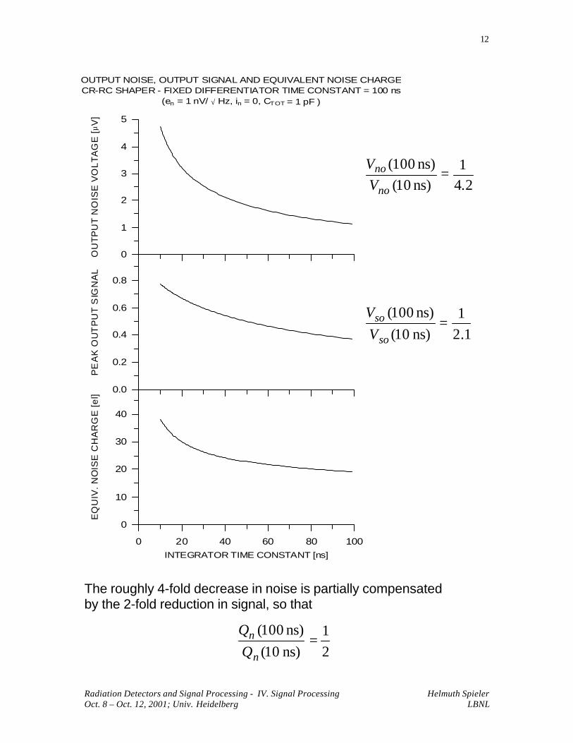
Consider a CR-RC shaper with a fixed differentiator timeconstant of 100 ns.
Increasing the integrator time constant lowers the uppercut-off frequency, which decreases the total noise at theshaper output.
However, the peak signal also decreases.
Still keeping the differentiator time constant fixed at 100 ns,the next set of graphs shows the variation of output noise and peaksignal as the integrator time constant is increased from 10 to 100 ns.
0 50 100 150 200 250 300
TIME [ns]
0.0
0.2
0.4
0.6
0.8
1.0
SH
AP
ER
OU
TP
UT
CR-RC SHAPERFIXED DIFFERENTIATOR TIME CONSTANT = 100 nsINTEGRATOR TIME CONSTANT = 10, 30 and 100 ns
τ int = 10 ns
τ int = 30 ns
τ int = 100 ns
Radiation Detectors and Signal Processing - IV. Signal Processing Helmuth SpielerOct. 8 – Oct. 12, 2001; Univ. Heidelberg LBNL
12
The roughly 4-fold decrease in noise is partially compensatedby the 2-fold reduction in signal, so that
0
1
2
3
4
5
OU
TP
UT
NO
ISE
VO
LT
AG
E [
µV
]
0.0
0.2
0.4
0.6
0.8
PE
AK
OU
TP
UT
SIG
NA
L
0 20 40 60 80 100
INTEGRATOR TIME CONSTANT [ns]
0
10
20
30
40
EQ
UIV
. N
OIS
E C
HA
RG
E [
el]
OUTPUT NOISE, OUTPUT SIGNAL AND EQUIVALENT NOISE CHARGECR-RC SHAPER - FIXED DIFFERENTIATOR TIME CONSTANT = 100 ns
(en = 1 nV/ √ Hz, in = 0, CTOT = 1 pF )
2.41
ns) 10(ns) 100(
=no
no
VV
1.21
ns) 10(
ns) 100(=
so
so
V
V
21
ns) 10(
ns) 100(=
n
n
Q
Q

Radiation Detectors and Signal Processing - IV. Signal Processing Helmuth SpielerOct. 8 – Oct. 12, 2001; Univ. Heidelberg LBNL
13
For comparison, consider the same CR-RC shaper with theintegrator time constant fixed at 10 ns and the differentiator timeconstant variable.
As the differentiator time constant is reduced, the peak signalamplitude at the shaper output decreases.
Note that the need to limit the pulse width incurs a significantreduction in the output signal.
Even at a differentiator time constant τdiff = 100 ns = 10 τint
the output signal is only 80% of the value for τdiff = ∞, i.e. a systemwith no low-frequency roll-off.
0 50 100 150 200 250 300
TIME [ns]
0.0
0.2
0.4
0.6
0.8
1.0
SH
AP
ER
OU
TP
UT
CR-RC SHAPERFIXED INTEGRATOR TIME CONSTANT = 10 ns
DIFFERENTIATOR TIME CONSTANT = ∞ , 100, 30 and 10 ns
τ diff = 10 ns
τ diff = 30 ns
τ diff = 100 ns
τ diff = ∞

Radiation Detectors and Signal Processing - IV. Signal Processing Helmuth SpielerOct. 8 – Oct. 12, 2001; Univ. Heidelberg LBNL
14
Although the noise grows as the differentiator time constant isincreased from 10 to 100 ns, it is outweighed by the increase in signallevel, so that the net signal-to-noise ratio improves.
0
1
2
3
4
5
OU
TP
UT
NO
ISE
VO
LT
AG
E [
µV
]
0.0
0.2
0.4
0.6
0.8
PE
AK
OU
TP
UT
SIG
NA
L
0 20 40 60 80 100
DIFFERENTIATOR TIME CONSTANT [ns]
0
10
20
30
40
50
60
70
EQ
UIV
. N
OIS
E C
HA
RG
E [
el]
OUTPUT NOISE, OUTPUT SIGNAL AND EQUIVALENT NOISE CHARGECR-RC SHAPER - FIXED INTEGRATOR TIME CONSTANT = 10 ns
(en = 1 nV/ √ Hz, in = 0, CTOT = 1 pF )
6.11
ns) 10(
ns) 100(=
n
n
Q
Q
3.1ns) 10(ns) 100(
=no
no
VV
1.2ns) 10(
ns) 100(=
so
so
V
V

Radiation Detectors and Signal Processing - IV. Signal Processing Helmuth SpielerOct. 8 – Oct. 12, 2001; Univ. Heidelberg LBNL
15
Summary
To evaluate shaper noise performance
• Noise spectrum alone is inadequate
Must also
• Assess effect on signal
Signal amplitude is also affected by the relationship of the shapingtime to the detector signal duration.
If peaking time of shaper < collection time
⇒⇒ signal loss (“ballistic deficit”)

Radiation Detectors and Signal Processing - IV. Signal Processing Helmuth SpielerOct. 8 – Oct. 12, 2001; Univ. Heidelberg LBNL
16
Ballistic Deficit
0 50 100TIME [ns]
0.0
0.5
1.0
AM
PL
ITU
DE
DETECTOR SIGNAL CURRENT
Loss in Pulse Height (and Signal-to-Noise Ratio) ifPeaking Time of Shaper < Detector Collection Time
Note that although the faster shaper has a peaking time of 5 ns, the response to the detector signal peaks after full charge collection.
SHAPER PEAKING TIME = 5 ns
SHAPER PEAKING TIME = 30 ns

Radiation Detectors and Signal Processing - IV. Signal Processing Helmuth SpielerOct. 8 – Oct. 12, 2001; Univ. Heidelberg LBNL
17
3. Evaluation of Equivalent Noise Charge
A. Experiment
Inject an input signal with known charge using a pulse generatorset to approximate the detector signal (possible ballistic deficit).Measure the pulse height spectrum.
peak centroid ⇒⇒ signal magnitude
peak width ⇒⇒ noise (FWHM= 2.35 rms)
If pulse-height digitization is not practical:
1. Measure total noise at output of pulse shaper
a) measure the total noise power with an rms voltmeter ofsufficient bandwidthor
b) measure the spectral distribution with a spectrumanalyzer and integrate (the spectrum analyzer providesdiscrete measurement values in N frequency bins ∆fn )
The spectrum analyzer shows if “pathological” features arepresent in the noise spectrum.
2. Measure the magnitude of the output signal Vso for a knowninput signal, either from detector or from a pulse generatorset up to approximate the detector signal.
3. Determine signal-to-noise ratio S/N= Vso / Vno
and scale to obtain the equivalent noise charge
( )2
0
( ) N
no non
V v n f=
= ⋅ ∆∑
sso
non Q
VV
Q =

Radiation Detectors and Signal Processing - IV. Signal Processing Helmuth SpielerOct. 8 – Oct. 12, 2001; Univ. Heidelberg LBNL
18
B. Numerical Simulation (e.g. SPICE)
This can be done with the full circuit including all extraneouscomponents. Procedure analogous to measurement.
1. Calculate the spectral distribution and integrate
2. Determine the magnitude of output signal Vso for an inputthat approximates the detector signal.
3. Calculate the equivalent noise charge
C. Analytical Simulation
1. Identify individual noise sources and refer to input
2. Determine the spectral distribution at input for each source k
3. Calculate the total noise at shaper output (G(f) = gain)
4. Determine the signal output Vso for a known input charge Qs
and realistic detector pulse shape.
5. Equivalent noise charge
2, ( )ni kv f
sso
non Q
VV
Q =
2
0
( ) N
no non
V v n f=
= ⋅ ∆∑
sso
non Q
VV
Q =
2 2
0 0
ω ω ω∞ ∞
= ≡ ∑ ∑∫ ∫
2 2, , ( ) ( ) ( ) ( ) no ni k n i k
k k
V G f v f df G v d

Radiation Detectors and Signal Processing - IV. Signal Processing Helmuth SpielerOct. 8 – Oct. 12, 2001; Univ. Heidelberg LBNL
19
Analytical Analysis of a Detector Front-End
Detector bias voltage is applied through the resistor RB. The bypasscapacitor CB serves to shunt any external interference comingthrough the bias supply line to ground. For AC signals this capacitorconnects the “far end” of the bias resistor to ground, so that RBappears to be in parallel with the detector.
The coupling capacitor CC in the amplifier input path blocks thedetector bias voltage from the amplifier input (which is why acapacitor serving this role is also called a “blocking capacitor”).
The series resistor RS represents any resistance present in theconnection from the detector to the amplifier input. This includes
• the resistance of the detector electrodes
• the resistance of the connecting wires
• any resistors used to protect the amplifier againstlarge voltage transients (“input protection”)
• ... etc.
OUTPUT
DETECTOR
BIASRESISTOR
Rb
Cc Rs
Cb
Cd
DETECTOR BIAS
PULSE SHAPERPREAMPLIFIER

Radiation Detectors and Signal Processing - IV. Signal Processing Helmuth SpielerOct. 8 – Oct. 12, 2001; Univ. Heidelberg LBNL
20
Equivalent circuit for noise analysis
bias shunt series equivalent input noisecurrent resistance resistance of amplifiershot thermal thermalnoise noise noise
In this example a voltage-sensitive amplifier is used, so all noisecontributions will be calculated in terms of the noise voltageappearing at the amplifier input.
Resistors can be modeled either as voltage or current generators.
• Resistors in parallel with the input act as current sources
• Resistors in series with the input act as voltage sources.
Steps in the analysis:
1. Determine the frequency distribution of the noise voltagepresented to the amplifier input from all individual noisesources
2. Integrate over the frequency response of a CR-RC shaper todetermine the total noise output.
3. Determine the output signal for a known signal charge andcalculate equivalent noise charge (signal charge for S/N= 1)
DETECTOR
Cd
BIASRESISTOR
SERIESRESISTOR
AMPLIFIER + PULSE SHAPER
Rb
Rs
i
i i
e
e
nd
nb na
ns
na

Radiation Detectors and Signal Processing - IV. Signal Processing Helmuth SpielerOct. 8 – Oct. 12, 2001; Univ. Heidelberg LBNL
21
Noise Contributions
1. Detector bias current
This model results from two assumptions:
1. The input impedance of the amplifier is infinite
2. The shunt resistance RP is much larger than the capacitivereactance of the detector in the frequency range of the pulseshaper.
Does this assumption make sense?
If RP is too small, the signal charge on the detectorcapacitance will discharge before the shaper outputpeaks. To avoid this
where ωP is the midband frequency of the shaper.Therefore,
as postulated.
PPDP tCR
ω1
≈>>
DPP C
Rω
1>>
CDend2qe DIind
2=

Radiation Detectors and Signal Processing - IV. Signal Processing Helmuth SpielerOct. 8 – Oct. 12, 2001; Univ. Heidelberg LBNL
22
Under these conditions the noise current will flow through thedetector capacitance, yielding the voltage
⇒⇒ the noise contribution decreases with increasing frequency (shorter shaping time)
Note: Although shot noise is “white”, the resulting noisespectrum is strongly frequency dependent.
In the time domain this result is more intuitive. Since every shaperalso acts as an integrator, one can view the total shot noise as theresult of “counting electrons”.
Assume an ideal integrator that records all charge uniformly within atime T. The number of electron charges measured is
The associated noise is the fluctuation in the number of electroncharges recorded
Does this also apply to an AC-coupled system, where no DC currentflows, so no electrons are “counted”?
Since shot noise is a fluctuation, the current undergoes bothpositive and negative excursions. Although the DC component isnot passed through an AC coupled system, the excursions are.Since, on the average, each fluctuation requires a positive and anegative zero crossing, the process of “counting electrons” isactually the counting of zero crossings, which in a detailedanalysis yields the same result.
( ) ( )2222
12
1
DDe
Dndnd
CIq
Cie
ωω==
e
De q
TIN =
TN en ∝=σ
Radiation Detectors and Signal Processing - IV. Signal Processing Helmuth SpielerOct. 8 – Oct. 12, 2001; Univ. Heidelberg LBNL
23
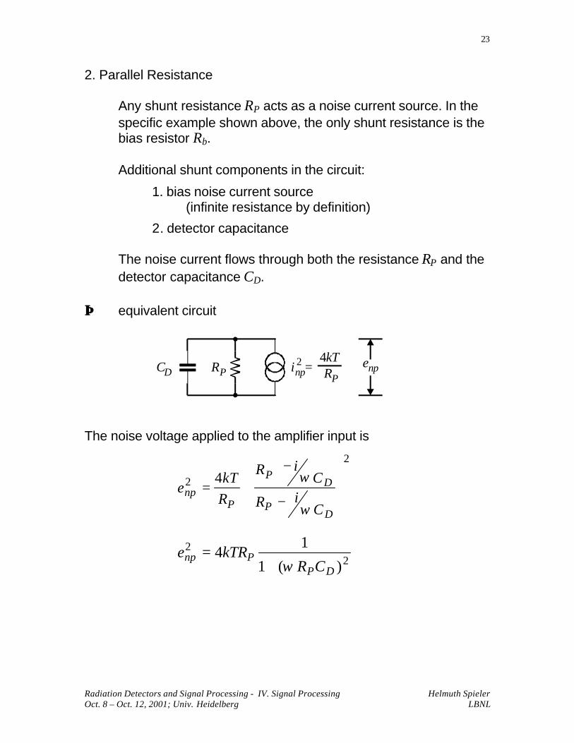
2. Parallel Resistance
Any shunt resistance RP acts as a noise current source. In thespecific example shown above, the only shunt resistance is thebias resistor Rb.
Additional shunt components in the circuit:
1. bias noise current source(infinite resistance by definition)
2. detector capacitance
The noise current flows through both the resistance RP and the detector capacitance CD.
⇒⇒ equivalent circuit
The noise voltage applied to the amplifier input is
2
2
4
−
−⋅=
DP
DP
Pnp
CiR
CiR
RkT
e
ω
ω
22
) (1
14
DPPnp
CRkTRe
ω+=
CD R RPP
4kT enpinp2 =

Radiation Detectors and Signal Processing - IV. Signal Processing Helmuth SpielerOct. 8 – Oct. 12, 2001; Univ. Heidelberg LBNL
24
Comment:
Integrating this result over all frequencies yields
which is independent of RP. Commonly referred to as “kTC ”noise, this contribution is often erroneously interpreted as the“noise of the detector capacitance”.
An ideal capacitor has no thermal noise; all noise originates inthe resistor.
So, why is the result independent of RP?
RP determines the primary noise, but also the noise bandwidthof this subcircuit. As RP increases, its thermal noise increases,but the noise bandwidth decreases, making the total noiseindependent of RP.
However,If one integrates enp over a bandwidth-limited system
the total noise decreases with increasing RP.
DDP
Pnp C
kTd
CR
kTRde =
+= ∫∫
∞∞
ωω
ωω ) (1
4)(
02
0
2
∫∞
−=
0
22
1) (
4 ωω
ωd
CRiiG
kTREDP
Pn

Radiation Detectors and Signal Processing - IV. Signal Processing Helmuth SpielerOct. 8 – Oct. 12, 2001; Univ. Heidelberg LBNL
25
3. Series Resistance
The noise voltage generator associated with the seriesresistance RS is in series with the other noise sources, so itsimply contributes
4. Amplifier input noise
The amplifier noise voltage sources usually are not physicallypresent at the amplifier input. Instead the amplifier noiseoriginates within the amplifier, appears at the output, and isreferred to the input by dividing the output noise by the amplifiergain, where it appears as a noise voltage generator.
↑ ↑“white 1/f noise noise” (can also originate in
external components)
This noise voltage generator also adds in series with the othersources.
• Amplifiers generally also exhibit input current noise, which isphysically present at the input. Its effect is the same as for thedetector bias current, so the analysis given in 1. can be applied.
Snr kTRe 42 =
f
Aee
fnwna 22 +=

Radiation Detectors and Signal Processing - IV. Signal Processing Helmuth SpielerOct. 8 – Oct. 12, 2001; Univ. Heidelberg LBNL
26
Determination of equivalent noise charge
1. Calculate total noise voltage at shaper output
2. Determine peak pulse height at shaper output for a knowninput charge
3. Input signal for which S/N=1 yields equivalent noise charge
First, assume a simple CR-RC shaper with equal differentiation andintegration time constants τd = τi = τ , which in this special case isequal to the peaking time.
The equivalent noise charge
↑ ↑ ↑current noise voltage noise 1/f noise
∝ τ ∝ 1/τ independent
independent of CD ∝ CD2 of τ
∝ CD2
• Current noise is independent of detector capacitance,consistent with the notion of “counting electrons”.
• Voltage noise increases with detector capacitance(reduced signal voltage)
• 1/f noise is independent of shaping time.In general, the total noise of a 1/f source depends on theratio of the upper to lower cutoff frequencies, not on theabsolute noise bandwidth. If τd and τi are scaled by thesame factor, this ratio remains constant.
( )
+⋅++⋅
++
= 2
222
22 44
42
8 DfD
naSnaP
Den CAC
ekTRiRkT
Iqe
Qτ
τ

Radiation Detectors and Signal Processing - IV. Signal Processing Helmuth SpielerOct. 8 – Oct. 12, 2001; Univ. Heidelberg LBNL
27
The equivalent noise charge Qn assumes a minimum when thecurrent and voltage noise contributions are equal.
Typical Result
↑ ↑dominated by voltage noise current noise
For a CR-RC shaper the noise minimum obtains for τd = τi = τ .
This criterion does not hold for more sophisticated shapers.
Caution: Even for a CR-RC shaper this criterion only applies whenthe differentiation time constant is the primary parameter,i.e. when the pulse width must be constrained.
When the rise time, i.e. the integration time constant, is theprimary consideration, it is advantageous to make τd > τi,since the signal will increase more rapidly than the noise,as was shown previously
100
1000
10000
0.01 0.1 1 10 100
SHAPING TIME [µs]
EQ
UIV
ALE
NT
NO
ISE
CH
AR
GE
[el]
VOLTAGE NOISE
1/f NOISE
CURRENT NOISE

Radiation Detectors and Signal Processing - IV. Signal Processing Helmuth SpielerOct. 8 – Oct. 12, 2001; Univ. Heidelberg LBNL
28
Numerical expression for the noise of a CR-RC shaper(amplifier current noise negligible)
(note that some units are “hidden” in the numerical factors)
where
τ shaping time constant [ns]
IB detector bias current + amplifier input current [nA]
RP input shunt resistance [kΩ]
en equivalent input noise voltage spectral density [nV/√Hz]
C total input capacitance [pF]
Qn= 1 el corresponds to 3.6 eV in Si2.9 eV in Ge
(see Spieler and Haller, IEEE Trans. Nucl. Sci. NS-32 (1985) 419 )
]electrons [rms 106.3 106 12 22
2452
ττ
τC
eR
IQ nP
Bn ⋅+⋅+=

Radiation Detectors and Signal Processing - IV. Signal Processing Helmuth SpielerOct. 8 – Oct. 12, 2001; Univ. Heidelberg LBNL
29
Note:
For sources connected in parallel, currents are additive.
For sources connected in series, voltages are additive.
⇒⇒ In the detector community voltage and current noise are often called “series” and “parallel” noise.
The rest of the world uses equivalent noise voltage and current.
Since they are physically meaningful, use of these widely understood terms is preferable.

Radiation Detectors and Signal Processing - IV. Signal Processing Helmuth SpielerOct. 8 – Oct. 12, 2001; Univ. Heidelberg LBNL
30
CR-RC Shapers with Multiple Integrators
a. Start with simple CR-RC shaper and add additional integrators
(n= 1 to n= 2, ... n= 8) with the same time constant τ .
With additional integrators the peaking time Tp increases
Tp = nτ
0 5 10 15 20T/tau
0.0
0.1
0.2
0.3
0.4
SH
AP
ER
OU
TP
UT
n=1
n=2
n=4
n=6
n=8

Radiation Detectors and Signal Processing - IV. Signal Processing Helmuth SpielerOct. 8 – Oct. 12, 2001; Univ. Heidelberg LBNL
31
b) Time constants changed to preserve the peaking time(τn= τn=1 /n)
Increasing the number of integrators makes the output pulse moresymmetrical with a faster return to baseline.
⇒⇒ improved rate capability at the same peaking time
Shapers with the equivalent of 8 RC integrators are common.Usually, this is achieved with active filters (i.e. circuitry thatsynthesizes the bandpass with amplifiers and feedback networks).
0 1 2 3 4 5TIME
0.0
0.2
0.4
0.6
0.8
1.0
SH
APE
R O
UTP
UT
n=8
n=1
n=2
n=4
Radiation Detectors and Signal Processing - IV. Signal Processing Helmuth SpielerOct. 8 – Oct. 12, 2001; Univ. Heidelberg LBNL
32
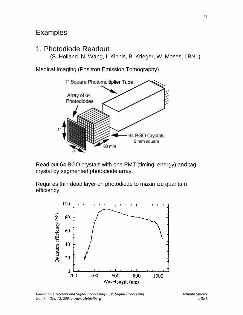
Examples
1. Photodiode Readout(S. Holland, N. Wang, I. Kipnis, B. Krieger, W. Moses, LBNL)
Medical Imaging (Positron Emission Tomography)
Read out 64 BGO crystals with one PMT (timing, energy) and tagcrystal by segmented photodiode array.
Requires thin dead layer on photodiode to maximize quantumefficiency.

Radiation Detectors and Signal Processing - IV. Signal Processing Helmuth SpielerOct. 8 – Oct. 12, 2001; Univ. Heidelberg LBNL
33
Thin electrode must be implemented with low resistance to avoidsignificant degradation of electronic noise.
Furthermore, low reverse bias current critical to reduce noise.
Photodiodes designed and fabricated in LBNL Microsystems Lab.
Front-end chip (preamplifier + shaper):
16 channels per chip
die size: 2 x 2 mm2,1.2 µm CMOS
continuously adjustable shaping time (0.5 to 50 µs)
gain: 100 mV per 1000 el.

Radiation Detectors and Signal Processing - IV. Signal Processing Helmuth SpielerOct. 8 – Oct. 12, 2001; Univ. Heidelberg LBNL
34
Noise vs. shaping time
Energy spectrum with BGO scintillator

Radiation Detectors and Signal Processing - IV. Signal Processing Helmuth SpielerOct. 8 – Oct. 12, 2001; Univ. Heidelberg LBNL
35
2. High-Rate X-Ray Spectroscopy(B. Ludewigt, C. Rossington, I. Kipnis, B. Krieger, LBNL)
Use detector with multiple strip electrodes
not for position resolution
but for
segmentation ⇒⇒ distribute rate over many channels
⇒⇒ reduced capacitance
⇒⇒ low noise at short shaping time
⇒⇒ higher rate per detector element
For x-ray energies 5 – 25 keV ⇒⇒ photoelectric absorption dominates (signal on 1 or 2 strips)
Strip pitch: 100 µm Strip Length: 2 mm (matched to ALS)

Radiation Detectors and Signal Processing - IV. Signal Processing Helmuth SpielerOct. 8 – Oct. 12, 2001; Univ. Heidelberg LBNL
36
Readout IC tailored to detector
Preamplifier + CR-RC2 shaper + cable driver to bank of parallel ADCs(M. Maier + H. Yaver)
Preamplifier with pulsed reset.
Shaping time continuously variable 0.5 to 20 µs.

Radiation Detectors and Signal Processing - IV. Signal Processing Helmuth SpielerOct. 8 – Oct. 12, 2001; Univ. Heidelberg LBNL
37
Chip wire-bonded to strip detector

Radiation Detectors and Signal Processing - IV. Signal Processing Helmuth SpielerOct. 8 – Oct. 12, 2001; Univ. Heidelberg LBNL
38
Initial results
Connecting detector increases noise because of added capacitanceand detector current (as indicated by increase of noise with peakingtime). Cooling the detector reduces the current and noise improves.
Second prototype
Current noise negligible because of cooling –“flat” noise vs. shaping time indicates that 1/f noise dominates.

Radiation Detectors and Signal Processing - IV. Signal Processing Helmuth SpielerOct. 8 – Oct. 12, 2001; Univ. Heidelberg LBNL
39
Measured spectra
55Fe
241Am

Radiation Detectors and Signal Processing - IV. Signal Processing Helmuth SpielerOct. 8 – Oct. 12, 2001; Univ. Heidelberg LBNL
40
Frequency vs. Time Domain
The noise analysis of shapers is rather straightforward if thefrequency response is known.
On the other hand, since we are primarily interested in the pulseresponse, shapers are often designed directly in the time domain, soit seems more appropriate to analyze the noise performance in thetime domain also.
Clearly, one can take the time response and Fourier transform it tothe frequency domain, but this approach becomes problematic fortime-variant shapers.
The CR-RC shapers discussed up to now utilize filters whose timeconstants remain constant during the duration of the pulse, i.e. theyare time-invariant.
Many popular types of shapers utilize signal sampling or change thefilter constants during the pulse to improve pulse characteristics, i.e.faster return to baseline or greater insensitivity to variations indetector pulse shape.
These time-variant shapers cannot be analyzed in the mannerdescribed above. Various techniques are available, but someshapers can be analyzed only in the time domain.
The basis of noise analysis in the time domain is Parseval’s Theorem
0
( ) ( ) ,∞ ∞
−∞
=∫ ∫A f df F t dt
which relates the spectral distribution of a signal in the frequencydomain to its time dependence. However, a more intuitive approachwill be used here.
First an example:
A commonly used time-variant filter is the correlated double-sampler.This shaper can be analyzed exactly only in the time domain.

Radiation Detectors and Signal Processing - IV. Signal Processing Helmuth SpielerOct. 8 – Oct. 12, 2001; Univ. Heidelberg LBNL
41
Correlated Double Sampling
1. Signals are superimposed on a (slowly) fluctuating baseline
2. To remove baseline fluctuations the baseline is sampled prior tothe arrival of a signal.
3. Next, the signal + baseline is sampled and the previous baselinesample subtracted to obtain the signal

Radiation Detectors and Signal Processing - IV. Signal Processing Helmuth SpielerOct. 8 – Oct. 12, 2001; Univ. Heidelberg LBNL
42
4. Noise Analysis in the Time Domain
What pulse shapes have a frequency spectrum corresponding totypical noise sources?
1. voltage noise
The frequency spectrum at the input of the detector system is“white”, i.e.
This is the spectrum of a δ impulse:
inifinitesimally narrow,but area = 1
2. current noise
The spectral density is inversely proportional to frequency, i.e.
This is the spectrum of a step impulse:
const. =dfdA
fdfdA 1
∝

Radiation Detectors and Signal Processing - IV. Signal Processing Helmuth SpielerOct. 8 – Oct. 12, 2001; Univ. Heidelberg LBNL
43
• Input noise can be considered as a sequence of δ and step pulseswhose rate determines the noise level.
• The shape of the primary noise pulses is modified by the pulseshaper:
δ pulses become longer,
step pulses are shortened.
• The noise level at a given measurement time Tm is determined bythe cumulative effect (superposition) of all noise pulses occurringprior to Tm .
• Their individual contributions at t= Tm are described by theshaper’s “weighting function” W(t).
References:
V. Radeka, Nucl. Instr. and Meth. 99 (1972) 525V. Radeka, IEEE Trans. Nucl. Sci. NS-21 (1974) 51F.S. Goulding, Nucl. Instr. and Meth. 100 (1972) 493F.S. Goulding, IEEE Trans. Nucl. Sci. NS-29 (1982) 1125

Radiation Detectors and Signal Processing - IV. Signal Processing Helmuth SpielerOct. 8 – Oct. 12, 2001; Univ. Heidelberg LBNL
44
Consider a single noise pulse occurring in a short time interval dtat a time T prior to the measurement. The amplitude at t= T is
an = W(T)
If, on the average, nn dt noise pulses occur within dt, the fluctuation oftheir cumulative signal level at t= T is proportional to
The magnitude of the baseline fluctuation is
For all noise pulses occurring prior to the measurement
wherenn determines the magnitude of the noise
and
describes the noise characteristics of theshaper – the “noise index”
dtnn
[ ]∫∞
∝0
22 )( dttWnnnσ
[ ] dttWnT nn2
2 )( )( ∝σ
[ ] dttW∫∞
0
2 )(

Radiation Detectors and Signal Processing - IV. Signal Processing Helmuth SpielerOct. 8 – Oct. 12, 2001; Univ. Heidelberg LBNL
45
The Weighting Function
a) current noise Wi (t) is the shaper response to a steppulse, i.e. the “normal” output waveform.
b) voltage noise
(Consider a δ pulse as the superposition oftwo step pulses of opposite polarity andspaced inifinitesimally in time)
Examples: 1. Gaussian 2. Trapezoid
current(“step”)noise
voltage(“delta”)noise
Goal: Minimize overall area to reduce current noise contributionMinimize derivatives to reduce voltage noise contribution
⇒⇒ For a given pulse duration a symmetrical pulse provides the best noise performance.Linear transitions minimize voltage noise contributions.
( ) ( ) '( )v id
W t W t W tdt
= ≡

Radiation Detectors and Signal Processing - IV. Signal Processing Helmuth SpielerOct. 8 – Oct. 12, 2001; Univ. Heidelberg LBNL
46
Time-Variant Shapers
Example: gated integrator with prefilter
The gated integrator integrates the input signal during a selectabletime interval (the “gate”).
In this example, the integrator is switched on prior to the signal pulseand switched off after a fixed time interval, selected to allow theoutput signal to reach its maximum.
Consider a noise pulse occurring prior to the “on time” of theintegrator.
occurrence of contribution of the noise pulse noise pulse to
integrator output

Radiation Detectors and Signal Processing - IV. Signal Processing Helmuth SpielerOct. 8 – Oct. 12, 2001; Univ. Heidelberg LBNL
47
For W1 = weighting function of the time-invariant prefilter
W2 = weighting function of the time-variant stage
the overall weighting function is obtained by convolution
Weighting function for current (“step”) noise: W(t)
Weighting function for voltage (“delta”) noise: W’(t)
Example
Time-invariant prefilter feeding a gated integrator(from Radeka, IEEE Trans. Nucl. Sci. NS-19 (1972) 412)
∫∞
∞−
−⋅= ' )'()'( )( 12 dtttWtWtW

Radiation Detectors and Signal Processing - IV. Signal Processing Helmuth SpielerOct. 8 – Oct. 12, 2001; Univ. Heidelberg LBNL
48
Comparison between a time-invariant and time-variant shaper(from Goulding, NIM 100 (1972) 397)
Example: trapezoidal shaper Duration= 2 µsFlat top= 0.2 µs
1. Time-Invariant Trapezoid
Current noise
Voltage noise
Minimum for τ1= τ3 (symmetry!) ⇒⇒ 2iN = 0.8, 2
vN = 2.2
3 )1( )]([ 31
20 0
2
3
2
2
1
221 2
1
3
2
τττ
ττ
τ τ
τ
τ
τ
++=
++
== ∫ ∫ ∫ ∫
∞
dtt
dtdtt
dttWN i
31
2
22
2 2
1 3 1 30 0
1 1 1 1[ '( )] vN W t dt dt dt
ττ
ττ τ τ τ
∞ = = + + = +
∫ ∫ ∫

Radiation Detectors and Signal Processing - IV. Signal Processing Helmuth SpielerOct. 8 – Oct. 12, 2001; Univ. Heidelberg LBNL
49
Gated Integrator Trapezoidal Shaper
Current Noise
Voltage Noise
⇒⇒ time-variant shaper 2iN = 1.4, 2
vN = 1.1
time-invariant shaper 2iN = 0.8, 2
vN = 2.2
time-variant trapezoid has more current noise, less voltage noise
∫ ∫ −=+
=
−T
I
TT
Ti
TTdtdt
Tt
NI
0
22
2
3)1( 2
2
2
0
1 22
T
vN dtT T
= = ∫

Radiation Detectors and Signal Processing - IV. Signal Processing Helmuth SpielerOct. 8 – Oct. 12, 2001; Univ. Heidelberg LBNL
50
Interpretation of Results
Example: gated integrator
Current Noise
Increases with T1 and TG ( i.e. width of W(t) )
( more noise pulses accumulate within width of W(t) )
Voltage Noise
Increases with the magnitude of the derivative of W(t)
( steep slopes → large bandwidth determined by prefilter )
Width of flat top irrelevant(δ response of prefilter is bipolar: net= 0)
∫∝ dttWQnv22 )]('[
∫∝ dttWQni22 )]([

Radiation Detectors and Signal Processing - IV. Signal Processing Helmuth SpielerOct. 8 – Oct. 12, 2001; Univ. Heidelberg LBNL
51
Quantitative Assessment of Noise in the Time Domain
(see Radeka, IEEE Trans. Nucl. Sci. NS-21 (1974) 51 )
↑↑ ↑↑current noise voltage noise
Qn= equivalent noise charge [C]
in= input current noise spectral density [A/√Hz]
en= input voltage noise spectral density [V/√Hz]
C = total capacitance at input
W(t) normalized to unit input step response
or rewritten in terms of a characteristic time t → T / t
2 2 2 2 2 21 1 12 2
[ ( )] [ '( )]n n nQ i T W t dt C e W t dtT
∞ ∞
−∞ −∞
= +∫ ∫
∫∫∞
∞−
∞
∞−
+= dttWeCdttWiQ nnn222222 )]('[
21
)]([ 21

Radiation Detectors and Signal Processing - IV. Signal Processing Helmuth SpielerOct. 8 – Oct. 12, 2001; Univ. Heidelberg LBNL
52
Correlated Double Sampling
1. Signals are superimposed on a (slowly) fluctuating baseline
2. To remove baseline fluctuations the baseline is sampled prior tothe arrival of a signal.
3. Next, the signal + baseline is sampled and the previous baselinesample subtracted to obtain the signal

Radiation Detectors and Signal Processing - IV. Signal Processing Helmuth SpielerOct. 8 – Oct. 12, 2001; Univ. Heidelberg LBNL
53
1. Current Noise
Current (shot) noise contribution:
Weighting function (T= time between samples):
Current noise coefficient
so that the equivalent noise charge
∫∞
∞−
= dttWiQ nni222 )]([
21
τ
τ
/)(
/
)( :
1)( : 0
0)( : 0
Tt
t
etWTt
etWTt
tWt
−−
−
=>
−=≤≤
=<
∫∞
∞−
= dttWFi2)]([
( ) ∫∫∞
−−− +−=T
TtT
ti dtedteF ττ /)(2
0
2/1
2
22/2/ τττ ττ +
−+= −− TT
i eeTF
( )
+−+= −− 1
2
2
1 /2/22 τττ TT
nni eeTiQ
+−+= −− 1
2
4
1 /2/22 ττ
ττ TT
nni eeT
iQ

Radiation Detectors and Signal Processing - IV. Signal Processing Helmuth SpielerOct. 8 – Oct. 12, 2001; Univ. Heidelberg LBNL
54
Reality Check 1:
Assume that the current noise is pure shot noise
so that
Consider the limit Sampling Interval >> Rise Time, T >> τ :
or expressed in electrons
where Ni is the number of electrons “counted” during the samplinginterval T.
Iqi en 22 =
TIqQ eni ⋅≈2
ee
eni q
TI
q
TIqQ
⋅=
⋅≈ 2
2
ini NQ ≈
+−+= −− 1
2
2
1 /2/2 ττ
ττ TT
eni eeT
IqQ

Radiation Detectors and Signal Processing - IV. Signal Processing Helmuth SpielerOct. 8 – Oct. 12, 2001; Univ. Heidelberg LBNL
55
2. Voltage Noise
Voltage Noise Contribution
Voltage Noise Coefficient
so that the equivalent noise charge
2 2 2 212
[ '( )]nv i nQ C e W t dt∞
−∞
= ∫
2[ '( )]vF W t dt∞
−∞
= ∫2 2
2
0
1 1/ ( ) / T
t t Tv
T
F e dt e dtτ τ
τ τ
∞− − − = +
∫ ∫
( )21 11
2 2/ T
vF e τ
τ τ−= − +
( )2 2 2 21 12
4/ T
nv i nQ C e e τ
τ−= −
( )212
2/ T
vF e τ
τ−= −
Radiation Detectors and Signal Processing - IV. Signal Processing Helmuth SpielerOct. 8 – Oct. 12, 2001; Univ. Heidelberg LBNL
56
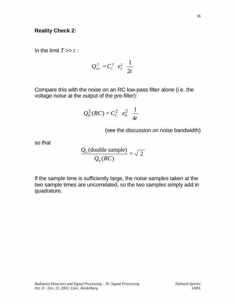
Reality Check 2:
In the limit T >> τ :
Compare this with the noise on an RC low-pass filter alone (i.e. thevoltage noise at the output of the pre-filter):
(see the discussion on noise bandwidth)
so that
If the sample time is sufficiently large, the noise samples taken at thetwo sample times are uncorrelated, so the two samples simply add inquadrature.
2 2 2 12nv i nQ C eτ
= ⋅ ⋅
τ41
)( 222 ⋅⋅= nin eCRCQ
2 )(
sample) double(=
RCQQ
n
n

Radiation Detectors and Signal Processing - IV. Signal Processing Helmuth SpielerOct. 8 – Oct. 12, 2001; Univ. Heidelberg LBNL
57
3. Signal Response
The preceding calculations are only valid for a signal response ofunity, which is valid at T >> τ.
For sampling times T of order τ or smaller one must correct for thereduction in signal amplitude at the output of the prefilter
so that the equivalent noise charge due to the current noise becomes
The voltage noise contribution is
and the total equivalent noise charge
τ/1 / Tis eVV −−=
22 2 2
2
1 2
4 1
/
/ ( )
T
nv i n T
eQ C v
e
τ
ττ
−
−
−=
−
2 2 n ni nvQ Q Q= +
( )2 /
/2/
22
1 4
12
τ
ττ
ττT
TT
nnie
eeT
iQ−
−−
−
+−+=

Radiation Detectors and Signal Processing - IV. Signal Processing Helmuth SpielerOct. 8 – Oct. 12, 2001; Univ. Heidelberg LBNL
58
Optimization
1. Noise current negligible
Parameters: T= 100 nsCd= 10 pFen= 2.5 nV/√Hz
→→ in= 6 fA/√Hz (Ib= 0.1 nA)
Noise attains shallow minimum for τ = T .
0
200
400
600
800
1000
1200
0 0.5 1 1.5 2 2.5 3
tau/T
Eq
uiv
alen
t N
ois
e C
har
ge
Qni [el]Qnv [el]Qn [el]

Radiation Detectors and Signal Processing - IV. Signal Processing Helmuth SpielerOct. 8 – Oct. 12, 2001; Univ. Heidelberg LBNL
59
2. Significant current noise contribution
Parameters: T= 100 nsCd= 10 pFen= 2.5 nV/√Hz
→→ in= 0.6 pA/√Hz (Ib= 1 µA)
Noise attains minimum for τ = 0.3 T .
0
1000
2000
3000
4000
5000
0 0.5 1 1.5 2 2.5 3
tau/T
Eq
uiv
alen
t N
ois
e C
har
ge
Qni [el]
Qnv [el]Qn [el]

Radiation Detectors and Signal Processing - IV. Signal Processing Helmuth SpielerOct. 8 – Oct. 12, 2001; Univ. Heidelberg LBNL
60
Parameters: T= 100 nsCd= 10 pFen= 2.5 nV/√Hz
→→ in= 0.2 pA/√Hz (Ib= 100 nA)
Noise attains minimum for τ = 0.5 T .
0
500
1000
1500
2000
0 0.5 1 1.5 2 2.5 3
tau/T
Eq
uiv
alen
t N
ois
e C
har
ge
Qni [el]Qnv [el]Qn [el]
Radiation Detectors and Signal Processing - IV. Signal Processing Helmuth SpielerOct. 8 – Oct. 12, 2001; Univ. Heidelberg LBNL
61
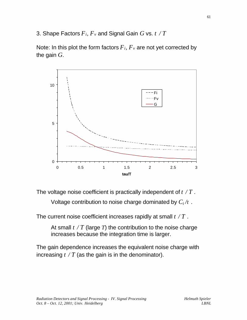
3. Shape Factors Fi, Fv and Signal Gain G vs. τ / T
Note: In this plot the form factors Fi, Fv are not yet corrected bythe gain G.
The voltage noise coefficient is practically independent of τ / T .
Voltage contribution to noise charge dominated by Ci /τ .
The current noise coefficient increases rapidly at small τ / T .
At small τ / T (large T) the contribution to the noise charge increases because the integration time is larger.
The gain dependence increases the equivalent noise charge withincreasing τ / T (as the gain is in the denominator).
0
5
10
0 0.5 1 1.5 2 2.5 3
tau/T
Fi
Fv
G

Radiation Detectors and Signal Processing - IV. Signal Processing Helmuth SpielerOct. 8 – Oct. 12, 2001; Univ. Heidelberg LBNL
62
5. Detector Noise Summary
Two basic noise mechanisms: input noise current ininput noise voltage en
Equivalent Noise Charge:
↑ ↑ ↑ ↑ ↑ ↑ front shaper front shaper front shaper end end end
where Ts Characteristic shaping time (e.g. peaking time)
Fi, Fv, Fvf “Shape Factors" that are determinedby the shape of the pulse.
They can be calculated in the frequency or time domain.
C Total capacitance at the input node(detector capacitance + input capacitance of preamplifier + stray capacitance + … )
Af 1/f noise intensity
• Current noise contribution increases with T
• Voltage noise contribution decreases with increasing T
Only for “white” voltage noise sources + capacitive load
“1/f ” voltage noise contribution constant in T
2 2 2 2 2 vn n s i n f vf
s
FQ i T F C e C A F
T= + +

Radiation Detectors and Signal Processing - IV. Signal Processing Helmuth SpielerOct. 8 – Oct. 12, 2001; Univ. Heidelberg LBNL
63
The shape factors Fi , Fv are easily calculated
[ ]2
212 2
( )( ) , S
i vS
T dW tF W t dt F dt
T dt
∞ ∞
−∞ −∞
= = ∫ ∫
where for time invariant pulse shaping W(t) is simply the system’simpulse response (the output signal seen on an oscilloscope) with thepeak output signal normalized to unity.
Typical values of Fi , FvCR-RC shaper Fi = 0.924 Fv = 0.924CR-(RC)4 shaper Fi = 0.45 Fv = 1.02
CR-(RC)7 shaper Fi = 0.34 Fv = 1.27CAFE chip Fi = 0.4 Fv = 1.2
Note that Fi < Fv for higher order shapers. Shapers can be optimizedto reduce current noise contribution relative to the voltage noise(mitigate radiation damage!).
“1/f ” noise contribution depends on the ratio of the upper to lowercutoff frequencies, so for a given shaper it is independent of shapingtime.

Radiation Detectors and Signal Processing - IV. Signal Processing Helmuth SpielerOct. 8 – Oct. 12, 2001; Univ. Heidelberg LBNL
64
1. Equivalent Noise Charge vs. Pulse Width
Current Noise vs. T
Voltage Noise vs. T
Total Equivalent Noise Charge

Radiation Detectors and Signal Processing - IV. Signal Processing Helmuth SpielerOct. 8 – Oct. 12, 2001; Univ. Heidelberg LBNL
65
2. Equivalent Noise Charge vs. Detector Capacitance (C = Cd + Ca)
If current noise in2FiT is negligible
↑ ↑ input shaper stage
Zero intercept
2 2 2 1 ( ) n n i d a n vQ i FT C C e F
T= + +
2
2 2 2
12
1 ( )
d n vn
dn i d a n v
C e FdQ TdC
i F T C C e FT
=
+ +
2 n vn
d
dQ Fe
dC T≈ ⋅
0 /
dn a n vC
Q C e F T=
=

Radiation Detectors and Signal Processing - IV. Signal Processing Helmuth SpielerOct. 8 – Oct. 12, 2001; Univ. Heidelberg LBNL
66
Noise slope is a convenient measure to compare preamplifiers andpredict noise over a range of capacitance.
Caution: both noise slope and zero intercept depend onboth the preamplifier and the shaper
Same preamplifier, but different shapers:
Caution: Noise slope is only valid when current noise negligible.
Current noise contribution may be negligible at highdetector capacitance, but not for Cd=0 where the voltage noise contribution is smaller.
2 2 2
0 /
dn n i a n vC
Q i FT C e F T=
= +

Radiation Detectors and Signal Processing - IV. Signal Processing Helmuth SpielerOct. 8 – Oct. 12, 2001; Univ. Heidelberg LBNL
67
6. Rate of Noise Pulses in Threshold DiscriminatorSystems
Noise affects not only the resolution of amplitude measurements, butalso the determines the minimum detectable signal threshold.
Consider a system that only records the presence of a signal if itexceeds a fixed threshold.
THRESHOLD ADJUST
TEST INPUT
GAIN/SHAPER COMPARATOR
DET.
PREAMP
OUTPUT
How small a detector pulse can still be detected reliably?

Radiation Detectors and Signal Processing - IV. Signal Processing Helmuth SpielerOct. 8 – Oct. 12, 2001; Univ. Heidelberg LBNL
68
Consider the system at times when no detector signal is present.
Noise will be superimposed on the baseline.
The amplitude distribution of the noise is gaussian.
↑ Baseline Level (E=0)
Radiation Detectors and Signal Processing - IV. Signal Processing Helmuth SpielerOct. 8 – Oct. 12, 2001; Univ. Heidelberg LBNL
69
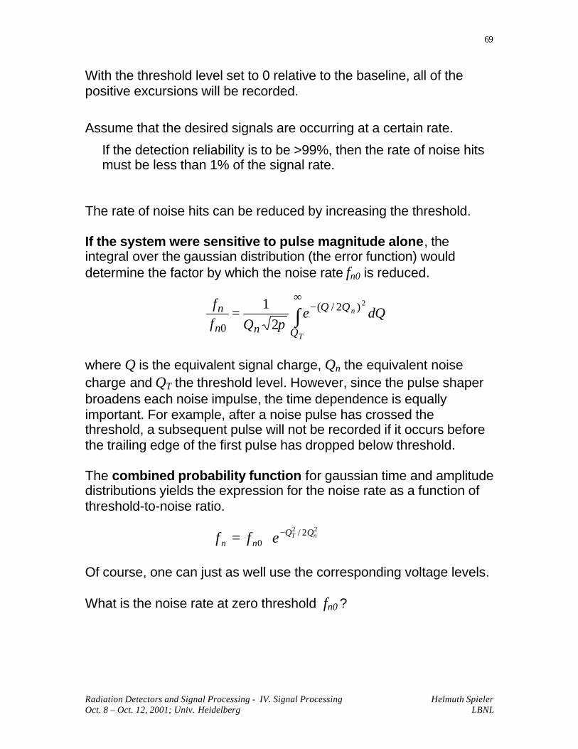
With the threshold level set to 0 relative to the baseline, all of thepositive excursions will be recorded.
Assume that the desired signals are occurring at a certain rate.
If the detection reliability is to be >99%, then the rate of noise hitsmust be less than 1% of the signal rate.
The rate of noise hits can be reduced by increasing the threshold.
If the system were sensitive to pulse magnitude alone, theintegral over the gaussian distribution (the error function) woulddetermine the factor by which the noise rate fn0 is reduced.
where Q is the equivalent signal charge, Qn the equivalent noisecharge and QT the threshold level. However, since the pulse shaperbroadens each noise impulse, the time dependence is equallyimportant. For example, after a noise pulse has crossed thethreshold, a subsequent pulse will not be recorded if it occurs beforethe trailing edge of the first pulse has dropped below threshold.
The combined probability function for gaussian time and amplitudedistributions yields the expression for the noise rate as a function ofthreshold-to-noise ratio.
Of course, one can just as well use the corresponding voltage levels.
What is the noise rate at zero threshold fn0 ?
∫∞
−=T
n
Q
nn
n dQeQf
f 2)2/(
0 2
1
π
22 2/0
nT QQnn eff −⋅=

Radiation Detectors and Signal Processing - IV. Signal Processing Helmuth SpielerOct. 8 – Oct. 12, 2001; Univ. Heidelberg LBNL
70
Since we are interested in the number of positive excursionsexceeding the threshold, fn0 is ½ the frequency of zero-crossings.
A rather lengthy analysis of the time dependence shows that thefrequency of zero crossings at the output of an ideal band-pass filterwith lower and upper cutoff frequencies f1 and f2 is
(Rice, Bell System Technical Journal, 23 (1944) 282 and 24 (1945) 46)
For a CR-RC filter with τi= τd the ratio of cutoff frequencies of thenoise bandwidth is
so to a good approximation one can neglect the lower cutofffrequency and treat the shaper as a low-pass filter, i.e. f1= 0. Then
An ideal bandpass filter has infinitely steep slopes, so the uppercutoff frequency f2 must be replaced by the noise bandwidth.
The noise bandwidth of an RC low-pass filter with time constant τ is
12
31
32
0 31
2ffff
f−−
=
5.41
2 =ff
20 3
2ff =
τ41
=∆ nf

Radiation Detectors and Signal Processing - IV. Signal Processing Helmuth SpielerOct. 8 – Oct. 12, 2001; Univ. Heidelberg LBNL
71
Setting f2 = ∆fn yields the frequency of zeros
and the frequency of noise hits vs. threshold
Thus, the required threshold-to-noise ratio for a given frequency ofnoise hits fn is
Note that the threshold-to-noise ratio determines the product of noiserate and shaping time, i.e. for a given threshold-to-noise ratio thenoise rate is higher at short shaping times
⇒⇒ The noise rate for a given threshold-to-noise ratio isproportional to bandwidth.
⇒⇒ To obtain the same noise rate, a fast system requires a largerthreshold-to-noise ratio than a slow system with the same noiselevel.
τ 32
10 =f
222222 2/2/02/0 34
12
nthnthnth QQQQQQnn ee
feff −−− ⋅=⋅=⋅=
τ
)34log(2 τnn
T fQQ
−=

Radiation Detectors and Signal Processing - IV. Signal Processing Helmuth SpielerOct. 8 – Oct. 12, 2001; Univ. Heidelberg LBNL
72
Frequently a threshold discriminator system is used in conjunctionwith other detectors that provide additional information, for examplethe time of a desired event.
In a collider detector the time of beam crossings is known, so theoutput of the discriminator is sampled at specific times.
The number of recorded noise hits then depends on
1. the sampling frequency (e.g. bunch crossing frequency) fS
2. the width of the sampling interval ∆t, which is determined by thetime resolution of the system.
The product fS ∆t determines the fraction of time the system is opento recording noise hits, so the rate of recorded noise hits is fS ∆t fn.
Often it is more interesting to know the probability of finding a noisehit in a given interval, i.e. the occupancy of noise hits, which can becompared to the occupancy of signal hits in the same interval.
This is the situation in a storage pipeline, where a specific timeinterval is read out after a certain delay time (e.g. trigger latency)
The occupancy of noise hits in a time interval ∆t
i.e. the occupancy falls exponentially with the square of the threshold-to-noise ratio.
22 2/
32nT QQ
nn et
ftP −⋅∆
=⋅∆=τ

Radiation Detectors and Signal Processing - IV. Signal Processing Helmuth SpielerOct. 8 – Oct. 12, 2001; Univ. Heidelberg LBNL
73
The dependence of occupancy on threshold can be used to measurethe noise level.
so the slope of log Pn vs. QT2 yields the noise level, independently of
the details of the shaper, which affect only the offset.
2
21
32loglog
−
∆
=n
Tn Q
QtP
τ
0.1 0.2 0.3 0.4 0.5 0.6 0.7 0.8 0.9 1.0 1.1
Threshold Squared [fC2
]
1.0E-6
1.0E-5
1.0E-4
1.0E-3
1.0E-2
1.0E-1
No
ise
Occ
up
ancy
Qn
= 1320 el

Radiation Detectors and Signal Processing - IV. Signal Processing Helmuth SpielerOct. 8 – Oct. 12, 2001; Univ. Heidelberg LBNL
74
7. Some Other Aspects of Pulse Shaping
7.1 Baseline Restoration
Any series capacitor in a system prevents transmission of a DCcomponent.
A sequence of unipolar pulses has a DC component that depends onthe duty factor, i.e. the event rate.
⇒⇒ The baseline shifts to make the overall transmittedcharge equal zero.
(from Knoll)
Random rates lead to random fluctuations of the baseline shift
⇒⇒ spectral broadening
• These shifts occur whenever the DC gain is not equal to themidband gain
The baseline shift can be mitigated by a baseline restorer (BLR).

Radiation Detectors and Signal Processing - IV. Signal Processing Helmuth SpielerOct. 8 – Oct. 12, 2001; Univ. Heidelberg LBNL
75
Principle of a baseline restorer:
Connect signal line to ground during theabsence of a signal to establish the baselinejust prior to the arrival of a pulse.
R1 and R2 determine the charge and discharge time constants.The discharge time constant (switch opened) must be much largerthan the pulse width.
Originally performed with diodes (passive restorer), baselinerestoration circuits now tend to include active loops with adjustablethresholds to sense the presence of a signal (gated restorer).Asymmetric charge and discharge time constants improveperformance at high count rates.
• This is a form of time-variant filtering. Care must be exercized toreduce noise and switching artifacts introduced by the BLR.
• Good pole-zero cancellation (next topic) is crucial for properbaseline restoration.
IN OUT
R R1 2

Radiation Detectors and Signal Processing - IV. Signal Processing Helmuth SpielerOct. 8 – Oct. 12, 2001; Univ. Heidelberg LBNL
76
3.2 Pole Zero Cancellation
Feedback capacitor in chargesensitive preamplifier must bedischarged. Commonly donewith resistor.
Output no longer a step,but decays exponentially
Exponential decaysuperimposed onshaper output.
⇒ undershoot
⇒ loss of resolution due to baseline variations
Add Rpz to differentiator:
“zero” cancels “pole” ofpreamp when RFCF = RpzCd
Not needed in pulsed reset circuits (optical or transistor)
Technique also used to compensate for “tails” of detector pulses:“tail cancellation”
Critical for proper functioning of baseline restorer.
TIME
SH
AP
ER
OU
TP
UT
TIME
PR
EA
MP
OU
TP
UT
TIME
SH
AP
ER
OU
TP
UT
CdRd
Rpz
CF
RF

Radiation Detectors and Signal Processing - IV. Signal Processing Helmuth SpielerOct. 8 – Oct. 12, 2001; Univ. Heidelberg LBNL
77
3.3 Bipolar vs. Unipolar Shaping
Unipolar pulse + 2nd differentiator →→ Bipolar pulse
Examples:
unipolar bipolar
Electronic resolution with bipolar shaping typ. 25 – 50% worse thanfor corresponding unipolar shaper.
However …
• Bipolar shaping eliminates baseline shift(as the DC component is zero).
• Pole-zero adjustment less critical
• Added suppression of low-frequency noise (see Part 7).
• Not all measurements require optimum noise performance.Bipolar shaping is much more convenient for the user
(important in large systems!) – often the method of choice.

Radiation Detectors and Signal Processing - IV. Signal Processing Helmuth SpielerOct. 8 – Oct. 12, 2001; Univ. Heidelberg LBNL
78
3.4 Pulse Pile-Up and Pile-Up Rejectors
pile-up ⇒⇒ false amplitude measurement
Two cases:
1. ∆T < time to peak
Both peak amplitudes areaffected by superposition.
⇒ Reject both pulses
Dead Time: ∆T + inspect time (~ pulse width)
2. ∆T > time to peak and∆T < inspect time, i.e.
time where amplitude of first pulse << resolution
Peak amplitude of first pulseunaffected.
⇒ Reject 2nd pulse only
No additional dead time if firstpulse accepted for digitizationand dead time of ADC >
(DT + inspect time)

Radiation Detectors and Signal Processing - IV. Signal Processing Helmuth SpielerOct. 8 – Oct. 12, 2001; Univ. Heidelberg LBNL
79
Typical Performance of a Pile-Up Rejector
(Don Landis)

Radiation Detectors and Signal Processing - IV. Signal Processing Helmuth SpielerOct. 8 – Oct. 12, 2001; Univ. Heidelberg LBNL
80
Dead Time and Resolution vs. Counting Rate
(Joe Jaklevic)
Throughput peaks and then drops as the input rate increases, as mostevents suffer pile-up and are rejected.
Resolution also degrades beyond turnover point.
• Turnover rate depends on pulse shape and PUR circuitry.
• Critical to measure throughput vs. rate!

Radiation Detectors and Signal Processing - IV. Signal Processing Helmuth SpielerOct. 8 – Oct. 12, 2001; Univ. Heidelberg LBNL
81
Limitations of Pile-Up Rejectors
Minimum dead time where circuitry can’t recognize second pulse
⇒ spurious sum peaks
Detectable dead time depends on relative pulse amplitudes
e.g. small pulse following large pulse
⇒ amplitude-dependent rejection factor
problem when measuring yields!
These effects can be evaluated and taken into account, but inexperiments it is often appropriate to avoid these problems by using ashorter shaping time (trade off resolution for simpler analysis).

Radiation Detectors and Signal Processing - IV. Signal Processing Helmuth SpielerOct. 8 – Oct. 12, 2001; Univ. Heidelberg LBNL
82
3.5 Delay-Line Clipping
In many instances, e.g. scintillation detectors, shaping is not used toimprove resolution, but to increase rate capability.
Example: delay line clipping with NaI(Tl) detector
_______________________________________________________
Reminder: Reflections on Transmission Lines
Termination < Line Impedance: Reflection with opposite signTermination > Line Impedance: Reflection with same sign
2td
TERMINATION: SHORT OPEN
REFLECTEDPULSE
PRIMARY PULSE
PULSE SHAPEAT ORIGIN

Radiation Detectors and Signal Processing - IV. Signal Processing Helmuth SpielerOct. 8 – Oct. 12, 2001; Univ. Heidelberg LBNL
83
The scintillation pulse has an exponential decay.
PMT Pulse
Reflected Pulse
Sum
Eliminate undershoot byadjusting magnitude ofreflected pulse
RT < Z0 , but RT > 0
magnitude of reflection= amplitude of detectorpulse at t = 2 td .
No undershoot atsumming node(“tail compensation”)
Only works perfectly for single decay time constant, but can still provideuseful results when other components are much faster (or weaker).

Radiation Detectors and Signal Processing - IV. Signal Processing Helmuth SpielerOct. 8 – Oct. 12, 2001; Univ. Heidelberg LBNL
84
4. Timing Measurements
Pulse height measurements discussed up to now emphasizeaccurate measurement of signal charge.
• Timing measurements optimize determination of time ofoccurrence.
• For timing, the figure of merit is not signal-to-noise,but slope-to-noise ratio.
Consider the leading edge of a pulse fed into a thresholddiscriminator (comparator).
The instantaneous signal level is modulated by noise.
⇒⇒ time of threshold crossing fluctuates
TV
nt
dtdV
σσ =

Radiation Detectors and Signal Processing - IV. Signal Processing Helmuth SpielerOct. 8 – Oct. 12, 2001; Univ. Heidelberg LBNL
85
Typically, the leading edge is not linear, so the optimum trigger levelis the point of maximum slope.
Pulse Shaping
Consider a system whose bandwidth is determined by a single RCintegrator.
The time constant of the RC low-pass filter determines the
• rise time (and hence dV/dt)• amplifier bandwidth (and hence the noise)
Time dependence:
The rise time is commonly expressed as the interval between thepoints of 10% and 90% amplitude
In terms of bandwidth
Example: An oscilloscope with 100 MHz bandwidth has3.5 ns rise time.
For a cascade of amplifiers:
)1()( /0
τto eVtV −−=
τ 2.2=rt
uur ff
t35.0
22.2
2.2 ===π
τ
... 222
21 rnrrr tttt +++≈

Radiation Detectors and Signal Processing - IV. Signal Processing Helmuth SpielerOct. 8 – Oct. 12, 2001; Univ. Heidelberg LBNL
86
Choice of Rise Time in a Timing System
Assume a detector pulse with peak amplitude V0 and a rise time tc
passing through an amplifier chain with a rise time tra.
If the amplifier rise time is longer than the signal rise time,
increase in bandwidth ⇒⇒ gain in dV/dt outweighs increase in noise.
In detail …
The cumulative rise time at the amplifier output (discriminator output)is
The electronic noise at the amplifier output is
For a single RC time constant the noise bandwidth
As the number of cascaded stages increases, the noise bandwidthapproaches the signal bandwidth. In any case
22racr ttt +=
nninino fedfeV ∆== ∫ 2
2
2
raun t
ff55.0
41
2===∆
τπ
ran t
f1
∝∆
ura
rau
ftdt
dV
tf
∝∝
∝∝
1
1 Noise

Radiation Detectors and Signal Processing - IV. Signal Processing Helmuth SpielerOct. 8 – Oct. 12, 2001; Univ. Heidelberg LBNL
87
The timing jitter
The second factor assumes a minimum when the rise time of theamplifier equals the collection time of the detector tra= tc.
At amplifier rise times greater than the collection time, the timeresolution suffers because of rise time degradation. For smalleramplifier rise times the electronic noise dominates.
The timing resolution improves with decreasing collection time √tc
and increasing signal amplitude V0.
111
0
22
000 c
ra
ra
ccrac
rarno
r
nonot t
ttt
V
ttt
tVtV
VtVV
dtdVV
+=+∝=≈=σ
0.1 1 10
t ra /t c
σσττ

Radiation Detectors and Signal Processing - IV. Signal Processing Helmuth SpielerOct. 8 – Oct. 12, 2001; Univ. Heidelberg LBNL
88
The integration time should be chosen to match the rise time.
How should the differentiation time be chosen?
As shown in the figure below, the loss in signal can be appreciableeven for rather large ratios τdif f /τint , e.g. >20% for τdiff /τint = 10.
Since the time resolution improves directly with increasing peaksignal amplitude, the differentiation time should be set to be as largeas allowed by the required event rate.
0 50 100 150 200 250 300
TIM E [ns]
0.0
0.2
0.4
0.6
0.8
1.0
SH
AP
ER
OU
TP
UT
CR-RC SHAPERFIXED INTEGRATOR TIME CONSTANT = 10 ns
DIFFERENTIATOR TIME CONSTANT = ∞ , 100, 30 and 10 ns
τ diff = 10 ns
τ diff = 30 ns
τ diff = 100 ns
τ diff = ∞

Radiation Detectors and Signal Processing - IV. Signal Processing Helmuth SpielerOct. 8 – Oct. 12, 2001; Univ. Heidelberg LBNL
89
Time Walk
For a fixed trigger level the time of threshold crossing depends onpulse amplitude.
⇒⇒ Accuracy of timing measurement limited by
• jitter (due to noise)
• time walk (due to amplitude variations)
If the rise time is known, “time walk” can be compensated in softwareevent-by-event by measuring the pulse height and correcting the timemeasurement.
This technique fails if both amplitude and rise time vary, as iscommon.
In hardware, time walk can be reduced by setting the threshold to thelowest practical level, or by using amplitude compensation circuitry,e.g. constant fraction triggering.

Radiation Detectors and Signal Processing - IV. Signal Processing Helmuth SpielerOct. 8 – Oct. 12, 2001; Univ. Heidelberg LBNL
90
Lowest Practical Threshold
Single RC integrator has maximum slope at t= 0.
However, the rise time of practically all fast timing systems isdetermined by multiple time constants.
For small t the slope at the output of a single RC integrator is linear,
so initially the pulse can be approximated by a ramp α t.
Response of the following integrator
⇒ The output is delayed by τ and curvature is introduced at small t.
Output attains 90% of input slope after t= 2.3τ.
Delay for n integrators= nτ
ττ
τ//
1)1( tt ee
dtd −− =−
τταταα / )( toi etVtV −−−=→=

Radiation Detectors and Signal Processing - IV. Signal Processing Helmuth SpielerOct. 8 – Oct. 12, 2001; Univ. Heidelberg LBNL
91
Additional RC integrators introduce more curvature at the beginningof the pulse.
Output pulse shape for multiple RC integrators
(normalized to preserve the peaking time τn= τn=1 /n)
Increased curvature at beginning of pulse limits the minimumthreshold for good timing.
⇒⇒ One dominant time constant best for timing measurements
Unlike amplitude measurements, where multiple integrators aredesirable to improve pulse symmetry and count rate performance.
0 1TIME
0.0
0.2
0.4
0.6
0.8
1.0
SH
AP
ER
OU
TP
UT
n=8
n=1
n=2
n=4

Radiation Detectors and Signal Processing - IV. Signal Processing Helmuth SpielerOct. 8 – Oct. 12, 2001; Univ. Heidelberg LBNL
92
Constant Fraction Timing
Basic Principle:
make the threshold track the signal
The threshold is derived from the signal by passing it through anattenuator VT = f Vs.
The signal applied to the comparator input is delayed so that thetransition occurs after the threshold signal has reached its maximumvalue VT = f V0 .

Radiation Detectors and Signal Processing - IV. Signal Processing Helmuth SpielerOct. 8 – Oct. 12, 2001; Univ. Heidelberg LBNL
93
For simplicity assume a linear leading edge
so the signal applied to the input is
When the input signal crosses the threshold level
and the comparator fires at the time
at a constant fraction of the rise time independent of peak amplitude.
If the delay td is reduced so that the pulse transitions at the signal andthreshold inputs overlap, the threshold level
and the comparator fires at
independent of both amplitude and rise time (amplitude and rise-timecompensation).
rrr
ttVtVttVtt
tV >=≤= for )( and for )( 00
0)( Vt
tttV
r
d−=
00 Vt
ttVf
r
d−=
)( rddr ttttft >+=
0Vtt
fVr
T =
00 Vt
ttV
tt
fr
d
r
−=
) )1(( 1 rd
d tftf
tt −<
−=

Radiation Detectors and Signal Processing - IV. Signal Processing Helmuth SpielerOct. 8 – Oct. 12, 2001; Univ. Heidelberg LBNL
94
The circuit compensates for amplitude and rise time if pulses have asufficiently large linear range that extrapolates to the same origin.
The condition for the delay must be met for the minimum rise time:
In this mode the fractional threshold VT /V0 varies with rise time.
For all amplitudes and rise times within the compensation range thecomparator fires at the time
min, )1( rd tft −≤
ft
t d
−=
10

Radiation Detectors and Signal Processing - IV. Signal Processing Helmuth SpielerOct. 8 – Oct. 12, 2001; Univ. Heidelberg LBNL
95
Another View of Constant Fraction Discriminators
The constant fraction discriminator can be analyzed as a pulseshaper, comprising the
• delay• attenuator• subtraction
driving a trigger that responds to the zero crossing.
The timing jitter depends on
• the slope at the zero-crossing(depends on choice of f and td )
• the noise at the output of the shaper(this circuit increases the noise bandwidth)

Radiation Detectors and Signal Processing - IV. Signal Processing Helmuth SpielerOct. 8 – Oct. 12, 2001; Univ. Heidelberg LBNL
96
Examples
1. γγ -γγ coincidence (as used in positron emission tomography)
Positron annihilation emits two collinear 511 keV photons.
Each detector alone will register substantial background.
Non-coincident background can be suppressed by requiringsimultaneous signals from both detectors.
• Each detector feeds a fast timing channel.
• The timing pulses are combined in an AND gate (coincidenceunit). The AND gate only provides an output if the two timingpulses overlap.
• The coincidence output is used to open a linear gate, that allowsthe energy signal to pass to the ADC.

Radiation Detectors and Signal Processing - IV. Signal Processing Helmuth SpielerOct. 8 – Oct. 12, 2001; Univ. Heidelberg LBNL
97
This arrangement accommodates the contradictory requirements oftiming and energy measurements. The timing channels can be fast,whereas the energy channel can use slow shaping to optimize energyresolution (“fast-slow coincidence”).
Chance coincidence rate
Two random pulse sequences have some probability ofcoincident events.
If the event rates in the two channels are n1 and n2, and the
timing pulse widths are ∆t1 and ∆t2, the probabality of a pulsefrom the first source occuring in the total coincidence window is
The coincidence is “sampled” at a rate n2 , so the chancecoincidence rate is
i.e. in the arrangement shown above, the chance coincidencerate increases with the square of the source strength.
Example: n1 = n2 = 106 s-1
∆t1 = ∆t1 = 5 ns
⇒⇒ nc= 104 s-1
)( 2121 ttnnnc ∆+∆⋅⋅=
)( 2111 ttnP ∆+∆⋅=
21 nPnc ⋅=

Radiation Detectors and Signal Processing - IV. Signal Processing Helmuth SpielerOct. 8 – Oct. 12, 2001; Univ. Heidelberg LBNL
98
2. Nuclear Mass Spectroscopy by Time-of-Flight
Two silicon detectors
First detector thin, so that particle passes through it(transmission detector)
⇒ differential energy loss ∆E
Second detector thick enough to stop particle
⇒ Residual energy E
Measure time-of-flight ∆t between the two detectors
2)/( stEAEEZEEE tottot ∆⋅∝⋅∆∝+∆=

Radiation Detectors and Signal Processing - IV. Signal Processing Helmuth SpielerOct. 8 – Oct. 12, 2001; Univ. Heidelberg LBNL
99
“Typical” Results
Example 1
Flight path 20 cm, ∆t ≈ 50 ps FWHMσ t = 21 ps
(H. Spieler et al., Z. Phys. A278 (1976) 241)

Radiation Detectors and Signal Processing - IV. Signal Processing Helmuth SpielerOct. 8 – Oct. 12, 2001; Univ. Heidelberg LBNL
100
Example 2
1. ∆E-detector: 27 µm thick, A= 100 mm2, <E>=1.1.104 V/cm
2. E-detector: 142 µm thick, A= 100 mm2, <E>=2.104 V/cm
For 230 MeV 28Si: ∆E = 50 MeV ⇒⇒ Vs= 5.6 mVE = 180 MeV ⇒⇒ Vs= 106 mV
⇒⇒ ∆t = 32 ps FWHMσ t = 14 ps
Example 3
Two transmission detectors,
each 160 µm thick, A= 320 mm2
For 650 MeV/u 20Ne: ∆E = 4.6 MeV ⇒⇒ Vs= 800 µV
⇒⇒ ∆t = 180 ps FWHMσ t = 77 ps
For 250 MeV/u 20Ne: ∆E = 6.9 MeV ⇒⇒ Vs= 1.2 mV
⇒⇒ ∆t = 120 ps FWHMσ t = 52 ps

Radiation Detectors and Signal Processing - IV. Signal Processing Helmuth SpielerOct. 8 – Oct. 12, 2001; Univ. Heidelberg LBNL
101
Fast Timing: Comparison between theory and experiment
At S/N<100 the measured curve lies above the calculation becausethe timing discriminator limited the rise time.At high S/N the residual jitter of the time digitizer limits the resolution.
For more details on fast timing with semiconductor detectors,see H. Spieler, IEEE Trans. Nucl. Sci. NS-29/3 (1982) 1142.

Radiation Detectors and Signal Processing - IV. Signal Processing Helmuth SpielerOct. 8 – Oct. 12, 2001; Univ. Heidelberg LBNL
102
9. Digitization of Pulse Height and Time –Analog to Digital Conversion
For data storage and subsequent analysis the analog signal at theshaper output must be digitized.
Important parameters for ADCs used in detector systems:
1. ResolutionThe “granularity” of the digitized output
2. Differential Non-LinearityHow uniform are the digitization increments?
3. Integral Non-LinearityIs the digital output proportional to the analog input?
4. Conversion TimeHow much time is required to convert an analog signalto a digital output?
5. Count-Rate PerformanceHow quickly can a new conversion commence after completion of a prior one without introducing deleterious artifacts?
6. StabilityDo the conversion parameters change with time?
Instrumentation ADCs used in industrial data acquisition and controlsystems share most of these requirements. However, detectorsystems place greater emphasis on differential non-linearity andcount-rate performance. The latter is important, as detector signalsoften occur randomly, in contrast to measurement systems wheresignals are sampled at regular intervals.

Radiation Detectors and Signal Processing - IV. Signal Processing Helmuth SpielerOct. 8 – Oct. 12, 2001; Univ. Heidelberg LBNL
103
9.1 ADC Parameters
1. Resolution
Digitization incurs approximation, as a continuous signal distributionis transformed into a discrete set of values. To reduce the additionalerrors (noise) introduced by digitization, the discrete digital stepsmust correspond to a sufficiently small analog increment.
Simplistic assumption:
Resolution is defined by the number of output bits, e.g.
13 bits →→
True Measure: Channel Profile
Plot probability vs. pulse amplitude that a pulse height corresponding to a specific output bin is actually convertedto that address.
Ideal ADC:
output bin number:
Measurement accuracy:
• If all counts of a peak fall in one bin, the resolution is ∆V.
• If the counts are distributed over several (>4 or 5) bins,peak fitting can yield a resolution of 10-1 – 10-2 ∆V,if the distribution is known and reproducible (not necessarilya valid assumption for an ADC).
4102.18192
1 −⋅==∆VV

Radiation Detectors and Signal Processing - IV. Signal Processing Helmuth SpielerOct. 8 – Oct. 12, 2001; Univ. Heidelberg LBNL
104
In reality, the channel profile is not rectangular as sketched above.
Electronic noise in the threshold discrimination process thatdetermines the channel boundaries “smears” the transition fromone bin to the next.
Measured channel profile (13 bit ADC)
The profiles of adjacent channels overlap
0
0.2
0.4
0.6
0.8
1
1.2
344 345 346 347 348 349 350
Channel Number n
P(c
han
nel
n)

Radiation Detectors and Signal Processing - IV. Signal Processing Helmuth SpielerOct. 8 – Oct. 12, 2001; Univ. Heidelberg LBNL
105
Channel profile can be checked quickly by applying the output of aprecision pulser to the ADC.
If the pulser output has very low noise, i.e. the amplitude jitter is muchsmaller than the voltage increment corresponding to one ADCchannel or bin, all pulses will be converted to a single channel, withonly a small fraction appearing in the neighbor channels.
Example of an ADC whose digital resolution is greater than its analogresolution:
8192 ch conversion range (13 bits)
2048 ch conversion range (11 bits)
2K range provides maximum resolution – higher ranges superfluous.
0.0E+00
5.0E+05
1.0E+06
6740 6760 6780 6800 6820 6840 6860 6880
CHANNEL NUMBER
CO
UN
TS
0.0E+00
5.0E+05
1.0E+06
1675 1680 1685 1690 1695 1700 1705 1710
CHANNEL NUMBER
CO
UN
TS

Radiation Detectors and Signal Processing - IV. Signal Processing Helmuth SpielerOct. 8 – Oct. 12, 2001; Univ. Heidelberg LBNL
106
How much ADC Resolution is Required?
Example:
Detector resolution1.8 keV FWHM
Digitized spectra for various ADC resolutions (bin widths) ∆E:
∆E= 1.8 keV = 1 x FWHM ∆E= 0.72 keV = 0.4 x FWHM
∆E= 0.36 keV = 0.2 x FWHM ∆E= 0.18 keV = 0.1 x FWHM
Fitting can determine centroid position to fraction of bin width evenwith coarse digitization, if the line shape is known.
Five digitizing channels within a linewidth (FWHM) allow robust peakfitting and centroid finding, even for imperfectly known line shapesand overlapping peaks.
-6 -5 -4 -3 -2 -1 0 1 2 3 4 5 6
RELATIVE ENERGY [keV]
CO
UN
TS
-6 -5 -4 -3 -2 -1 0 1 2 3 4 5 6
RELATIVE ENERGY [keV]
CO
UN
TS
∆E = 1.8
-6 -5 -4 -3 -2 -1 0 1 2 3 4 5 6
RELATIVE ENERGY [keV]
CO
UN
TS
∆E = 0.72
-6 -5 -4 -3 -2 -1 0 1 2 3 4 5 6
RELATIVE ENERGY [keV]
CO
UN
TS
∆E = 0.36
-6 -5 -4 -3 -2 -1 0 1 2 3 4 5 6
RELATIVE ENERGY [keV]
CO
UN
TS
∆E = 0.18

Radiation Detectors and Signal Processing - IV. Signal Processing Helmuth SpielerOct. 8 – Oct. 12, 2001; Univ. Heidelberg LBNL
107
2. Differential Non-Linearity
Differential non-linearity is a measure of the inequality of channelprofiles over the range of the ADC.
Depending on the nature of the distribution, either a peak or an rmsspecification may be appropriate.
or
where is the average channel width and ∆V(i) is the width ofan individual channel.
Differential non-linearity of < ±1% max. is typical, but state-of-the-artADCs can achieve 10-3 rms, i.e. the variation is comparable to thestatistical fluctuation for 106 random counts.
Note: Instrumentation ADCs are often specified with an accuracy of±0.5 LSB (least significant bit), so the differential non-linearitymay be 50% or more.
Typical differential non-linearity patterns (“white” input spectrum).
An ideal ADC would show an equal number of counts in each bin.
The spectrum to the left shows a random pattern, but note themultiple periodicities visible in the right hand spectrum.
−∆
∆= 1
)( max
ViV
DNL
−∆
∆= 1
)(r.m.s.
ViV
DNL
V∆
CHANNEL NUMBER CHANNEL NUMBER
CO
UN
TS
CO
UN
TS

Radiation Detectors and Signal Processing - IV. Signal Processing Helmuth SpielerOct. 8 – Oct. 12, 2001; Univ. Heidelberg LBNL
108
3. Integral Non-Linearity
Integral non-linearity measures the deviation from proportionality ofthe measured amplitude to the input signal level.
The dots are measured values and the line is a fit to the data.
This plot is not very useful if the deviations from linearity are small.
Plotting the deviations of the measured points from the fit yields:
-20
-15
-10
-5
0
5
10
15
0 1000 2000 3000 4000 5000 6000 7000 8000 9000
Channel Number
Dev
iatio
n fro
m F
it [c
h]
0
1000
2000
3000
4000
5000
6000
7000
8000
9000
Pulse Height
Cha
nnel
Num
ber

Radiation Detectors and Signal Processing - IV. Signal Processing Helmuth SpielerOct. 8 – Oct. 12, 2001; Univ. Heidelberg LBNL
109
The linearity of an ADC can depend on the input pulse shape andduration, due to bandwidth limitations in the circuitry.
The differential non-linearity shown above was measured with a400 ns wide input pulse.
Increasing the pulse width to 3 µs improved the result significantly:
-2
-1
0
1
2
3
0 1000 2000 3000 4000 5000 6000 7000 8000 9000
Channel Number
Dev
iatio
n fro
m F
it [c
h]

Radiation Detectors and Signal Processing - IV. Signal Processing Helmuth SpielerOct. 8 – Oct. 12, 2001; Univ. Heidelberg LBNL
110
4. Conversion Time
During the acquisition of a signal the system cannot accept asubsequent signal (“dead time”)
Dead Time =
signal acquisition time → time-to-peak + const.
+ conversion time → can depend on pulse height
+ readout time to memory → depends on speed of data transmission and buffer memory access - can be large in computer- based systems
Dead time affects measurements of yields or reaction cross-sections. Unless the event rate << 1/(dead time), it is necessary tomeasure the dead time, e.g. with a reference pulser fedsimultaneously into the spectrum.
The total number of reference pulses issued during themeasurement is determiend by a scaler and compared with thenumber of pulses recorded in the spectrum.
Does a pulse-height dependent dead time mean that thecorrection is a function of pulse height?
Usually not. If events in different part of the spectrum are notcorrelated in time, i.e. random, they are all subject to the sameaverage dead time (although this average will depend on thespectral distribution).
• Caution with correlated events!Example: Decay chains, where lifetime is < dead time.
The daughter decay will be lost systematically.

Radiation Detectors and Signal Processing - IV. Signal Processing Helmuth SpielerOct. 8 – Oct. 12, 2001; Univ. Heidelberg LBNL
111
5. Count Rate Effects
Problems are usually due to internal baseline shifts with event rateor undershoots following a pulse.
If signals occur at constant intervals, the effect of anundershoot will always be the same.
However, in a random sequence of pulses, the effect will varyfrom pulse to pulse.
⇒⇒ spectral broadening
Baseline shifts tend to manifest themselves as a systematic shift incentroid position with event rate.
Centroid shifts for two 13 bit ADCs vs. random rate:
-10
-9
-8
-7
-6
-5
-4
-3
-2
-1
0
0 20 40 60 80 100 120 140
Signal Rate [103 s -1]
Cen
troid
Shi
ft [c
hann
els]

Radiation Detectors and Signal Processing - IV. Signal Processing Helmuth SpielerOct. 8 – Oct. 12, 2001; Univ. Heidelberg LBNL
112
6. Stability
Stability vs. temperature is usually adequate with modern electronics in a laboratory environment.
• Note that temperature changes within a module are typicallymuch smaller than ambient.
However: Highly precise or long-term measurements requirespectrum stabilization to compensate for changesin gain and baseline of the overall system.
Technique: Using precision pulsers place a reference peak atboth the low and high end of the spectrum.
(Pk. Pos. 2) – (Pk. Pos. 1) → Gain, … then
(Pk. Pos. 1) or (Pk. Pos. 2) → Offset
Traditional Implementation: Hardware,spectrum stabilizer module
Today, it is more convenient to determine the corrections insoftware. These can be applied to calibration corrections orused to derive an electrical signal that is applied to thehardware (simplest and best in the ADC).

Radiation Detectors and Signal Processing - IV. Signal Processing Helmuth SpielerOct. 8 – Oct. 12, 2001; Univ. Heidelberg LBNL
113
9.2 Analog to Digital Conversion Techniques
1. Flash ADC Vref
comparators decoder
data output
The input signal is applied to n comparators in parallel. The switchingthresholds are set by a resistor chain, such that the voltage differencebetween individual taps is equal to the desired measurementresolution.
2n comparators for n bits (8 bit resolution requires 256 comparators)
Feasible in monolithic ICs since the absolute value of the resistors inthe reference divider chain is not critical, only the relative matching.
Advantage: short conversion time (<10 ns available)Drawbacks: limited accuracy (many comparators)
power consumptionDifferential non-linearity ~ 1%High input capacitance (speed is often limited by the
analog driver feeding the input)

Radiation Detectors and Signal Processing - IV. Signal Processing Helmuth SpielerOct. 8 – Oct. 12, 2001; Univ. Heidelberg LBNL
114
2. Successive Approximation ADC
Pulse Stretcher Comparator Control Logic,Register + DAC
Output Address
Sequentially add levels proportional to2n, 2n-1, … 20 and set correspondingbit if the comparator output is high(DAC output < pulse height)
n conversion steps yield 2n channels,i.e. 8K channels require 13 steps
Advantages: speed (~ µs)high resolutionICs (monolithic + hybrid) available
Drawback: Differential non-linearity (typ. 10 – 20%)
Reason: Resistors that set DAC output must beextremely accurate.
For DNL < 1% the resistor determining the 212 level in an 8K ADC must be accurate to < 2.4 . 10-6.

Radiation Detectors and Signal Processing - IV. Signal Processing Helmuth SpielerOct. 8 – Oct. 12, 2001; Univ. Heidelberg LBNL
115
DNL can be corrected by various techniques:
• averaging over many channel profiles for a given pulseamplitude (“sliding scale” or “Gatti principle”)
• correction DAC (“brute force” application of IC technology)
The primary DAC output is adjusted by the output of a correctionDAC to reduce differential non-linearity.
Correction data are derived from a measurement of DNL.Corrections for each bit are loaded into the RAM, which actsas a look-up table to provide the appropriate value to thecorrection DAC for each bit of the main DAC.
The range of the correction DAC must exceed the peak-to-peakdifferential non-linearity.
If the correction DAC has N bits, the maximum DNL is reduced by2 - (N-1) (if deviations are symmetrical).
PULSESTRETCHER COMPARATOR
CONTROL LOGIC
DACADDRESS
LOAD CORRECTION DATA
SUMMINGAMPLIFIER
DAC
CORR.DAC
OUTIN
RAM∆V= DNLP-P
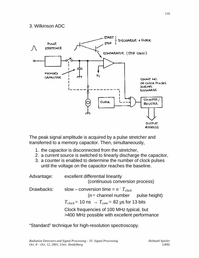
Radiation Detectors and Signal Processing - IV. Signal Processing Helmuth SpielerOct. 8 – Oct. 12, 2001; Univ. Heidelberg LBNL
116
3. Wilkinson ADC
The peak signal amplitude is acquired by a pulse stretcher andtransferred to a memory capacitor. Then, simultaneously,
1. the capacitor is disconnected from the stretcher,2. a current source is switched to linearly discharge the capacitor,3. a counter is enabled to determine the number of clock pulses
until the voltage on the capacitor reaches the baseline.
Advantage: excellent differential linearity(continuous conversion process)
Drawbacks: slow – conversion time = n . Tclock
(n= channel number ∝ pulse height)
Tclock= 10 ns → Tconv= 82 µs for 13 bits
Clock frequencies of 100 MHz typical, but >400 MHz possible with excellent performance
“Standard” technique for high-resolution spectroscopy.

Radiation Detectors and Signal Processing - IV. Signal Processing Helmuth SpielerOct. 8 – Oct. 12, 2001; Univ. Heidelberg LBNL
117
Hybrid Analog-to-Digital Converters
Conversion techniques can be combined to obtain high resolutionand short conversion time.
1. Flash + Successive Approximation orFlash + Wilkinson (Ramp Run-Down)
Utilize fast flash ADC for coarse conversion(e.g. 8 out of 13 bits)
Successive approximation or Wilkinson converter to provide fine resolution. Limited range, so short conversion time:
256 ch with 100 MHz clock ⇒ 2.6 µs
Results: 13 bit conversion in < 4 µswith excellent integral and differential linearity
2. Flash ADCs with Sub-Ranging
Not all applications require constant absolute resolutionover the full range. Sometimes only relative resolutionmust be maintained, especially in systems with a verylarge dynamic range.
Precision binary divider at input to determine coarse range+ fast flash ADC for fine digitization.
Example: Fast digitizer that fits in phototube base.Designed at FNAL.
17 to 18 bit dynamic rangeDigital floating point output
(4 bit exponent, 8+1 bit mantissa)16 ns conversion time

Radiation Detectors and Signal Processing - IV. Signal Processing Helmuth SpielerOct. 8 – Oct. 12, 2001; Univ. Heidelberg LBNL
118
9.3 Time Digitizers
1. Counter
Simplest arrangement.
Count clock pulses between start and stop.
Limitation: Speed of counter
Current technology limits speed of counter systemto about 1 GHz
⇒⇒ ∆t = 1 ns
Multi-hit capability
2. Analog Ramp
Commonly used in high-resolution digitizers (∆t = 10 ps)
Principle: charge capacitor through switchable current source
Start pulse: turn on current source
Stop pulse: turn off current source
⇒⇒ Voltage on storage capacitor
Use Wilkinson ADC with smaller discharge current to digitize voltage.
Drawbacks: No multi-hit capabilityDeadtime

Radiation Detectors and Signal Processing - IV. Signal Processing Helmuth SpielerOct. 8 – Oct. 12, 2001; Univ. Heidelberg LBNL
119
3. Digitizers with Clock Interpolation
Most experiments in HEP require multi-hit capability, no deadtime
Commonly used technique for time digitization (Y. Arai, KEK)
Clock period interpolated by inverter delays (U1, U2, …).Delay can be fine-tuned by adjusting operating point of inverters.
Delays stabilized by delay-locked loop
Devices with 250 ps resolution fabricated and tested.
see Y. Arai et al., IEEE Trans. Nucl. Sci. NS-45/3 (1998) 735-739and references therein.

Radiation Detectors and Signal Processing - IV. Signal Processing Helmuth SpielerOct. 8 – Oct. 12, 2001; Univ. Heidelberg LBNL
120
10. Digital Signal Processing
Sample detector signal with fast digitizer to reconstruct pulse:
Then use digital signal processor to perform mathematical operationsfor desired pulse shaping.
Block Diagram
DSP allows great flexibility in implementing filtering functions
However: increased circuit complexityincreased demands on ADC,
compared to traditional shaping.
0 10 20 30TIME [ns]
0.0
0.2
0.4
0.6
SIG
NA
L C
UR
RE
NT
INCIDENTRADIATION PUBLICATION
DETECTOR PREAMP ADC DSP
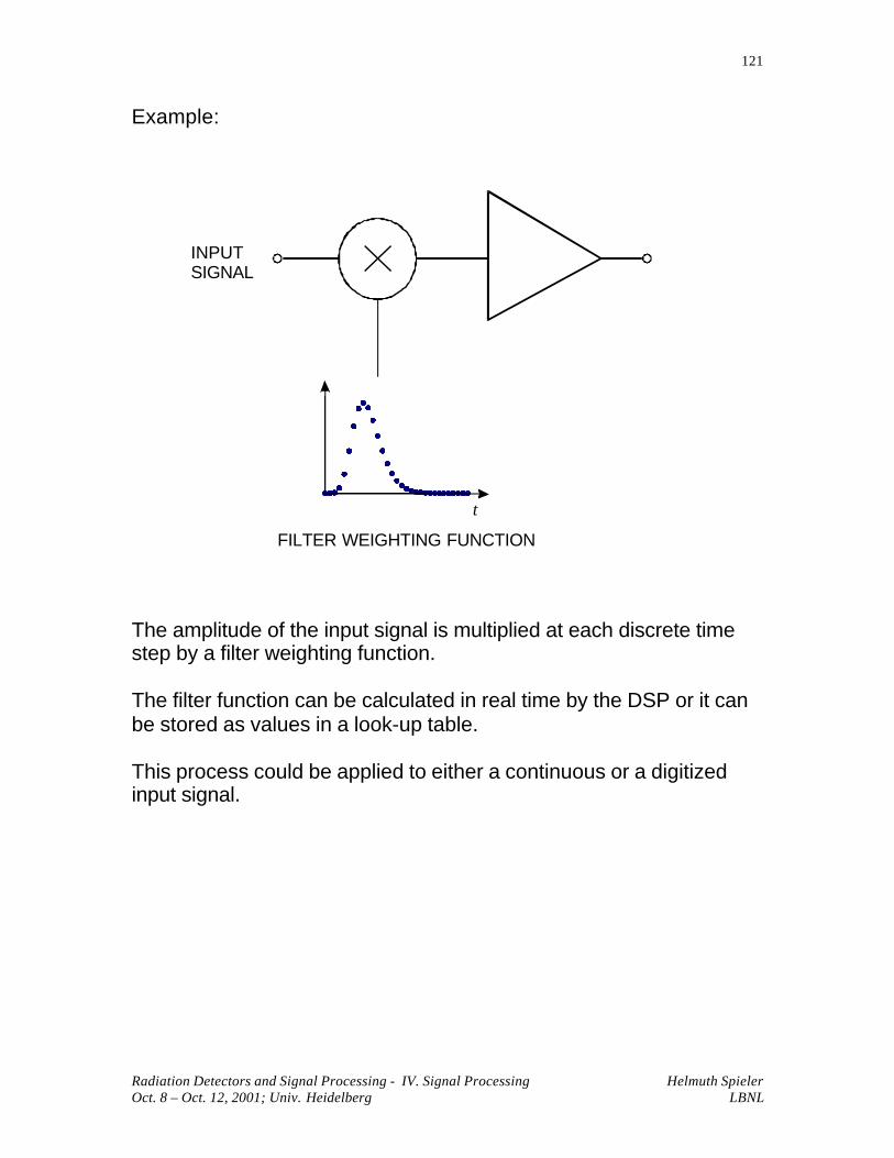
Radiation Detectors and Signal Processing - IV. Signal Processing Helmuth SpielerOct. 8 – Oct. 12, 2001; Univ. Heidelberg LBNL
121
Example:
The amplitude of the input signal is multiplied at each discrete timestep by a filter weighting function.
The filter function can be calculated in real time by the DSP or it canbe stored as values in a look-up table.
This process could be applied to either a continuous or a digitizedinput signal.
t
INPUTSIGNAL
FILTER WEIGHTING FUNCTION

Radiation Detectors and Signal Processing - IV. Signal Processing Helmuth SpielerOct. 8 – Oct. 12, 2001; Univ. Heidelberg LBNL
122
Important to choose sample interval sufficiently small to capture pulsestructure.
Sampling interval of 4 ns misses initial peak.
ADC must be capable of digitizing at greater than twice the rate of thehighest frequency component in the signal (Nyquist criterion).
With too low a sampling rate high frequency components will be“aliased” to lower frequencies:
“Aliasing” occurs in any sampling process – i.e. also in 2D or 3Dimage processing.
0 10 20 30TIME [ns]
0.0
0.2
0.4
0.6S
IGN
AL
CU
RR
EN
T
SAMPLING TIMES
T T T T T T T1 2 3 4 5 6 7
ACTUALWAVEFORM
ALIASEDWAVEFORM

Radiation Detectors and Signal Processing - IV. Signal Processing Helmuth SpielerOct. 8 – Oct. 12, 2001; Univ. Heidelberg LBNL
123
⇒⇒ Fast ADC required + Pre-Filter to limit signal bandwidth
• Dynamic range requirements for ADC may be more severe than inanalog filtered system (depending on pulse shape and pre-filter).
• ADC introduces additional noisequantization introduces quasi-random noise
σ∆
=12
Cn
V
where ∆V is the signal increment corresponding to 1 bit.– increased by differential non-linearity)
• Electronics preceding ADC and front-end of ADC must exhibitsame precision as analog system, i.e.
baseline and other pulse-to-pulse amplitude fluctuations less than order Qn /10, i.e. typically 10-4 in high-resolution systems.
For 10 V FS at the ADC input in a high-resolution gamma-ray detector system, this corresponds to < 1 mV.
⇒⇒ ADC must provide high performance at short conversion times
Today this is technically feasible for some applications, e.g. detectorswith moderate to long collection times (γ and x-ray detectors).
Systems commercially available.
DETECTOR PREAMP ADC DSPPRE-FILTER

Radiation Detectors and Signal Processing - IV. Signal Processing Helmuth SpielerOct. 8 – Oct. 12, 2001; Univ. Heidelberg LBNL
124
Benefits of digital signal processing:
• Flexibility in implementing filter functions
• Filters possible that are impractical in hardware
• Simple to change filter parameters
• Tail cancellation and pile-up rejection easily incorporated
• Adaptive filtering can be used to compensate for pulse shape variations.
Where is digital signal processing appropriate?
• Systems highly optimized for
Resolution
High counting rates
• Variable detector pulse shapes
Where is analog signal processing best (most efficient)?
• Fast shaping
• Systems not sensitive to pulse shape (fixed shaper constants)
• High density systems that require
small circuit area
low power
Both types of systems require careful analog design.
Progress in fast ADCs (precision, reduced power) will expandrange of DSP applications
Top Related