


Languages
Pages
Legal

Forschungszentrum Jülich
Ferroelectric Tunnel Junctions: A Theoretical Approach
H. Kohlstedt, A. Petraru, R. WaserForschungszentrum Jülich GmbH,
Institut für Festkörperforschung and CNI, the Center of Nanoelectronic Systems and Information Technology, Germany
N. A. PertsevA. F. Ioffe Physico-Technical Institute, St. Petersburg, Russia
Center ofNanoelectronic Systems Information Technology
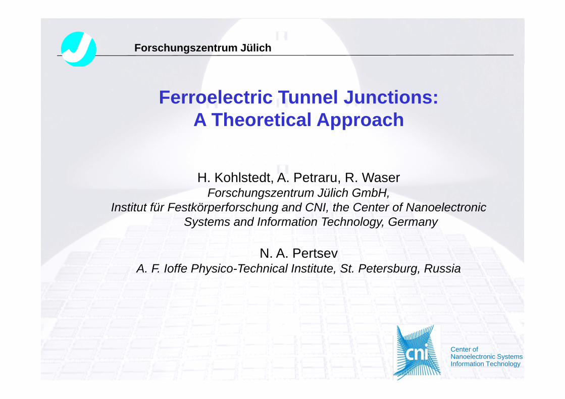
Electron Tunneling through Insulators
EWpotW )(xφW )(xφ
xt0
k xikCΨxk real xk xk real
Re BΨ
xikB
xeB=Ψxik
CxeC=Ψimaginary
x
⎪⎫⎪⎧ t
xikxA −Ψ
Re AΨ
⎪⎭
⎪⎬⎫
⎪⎩
⎪⎨⎧−= ∫ dxxmCT
t
0
)(22exp φh
AxeA=Ψ ⎭
Transmission coefficient
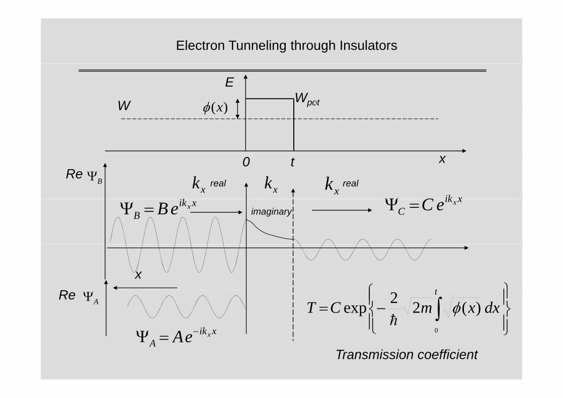
Electron tunneling: Current Transport Equation
Metal 1 Metal 2I
Fermi distributions of(occupied/unoccupied) states
Fermi distributions of( i d/ i d) t tj
j2-1(occupied/unoccupied) states
+ eVT
j1-2
dd
−− −=−=
jjjdirectionxdensitycurrentnvej x
1221
:
[ ] ⊥⊥
∞
⋅−= ∫∫⊥
⊥dkkTEfEfdEej
k
kE
max)(
),(213 )()(4 hπ o 04 hπ
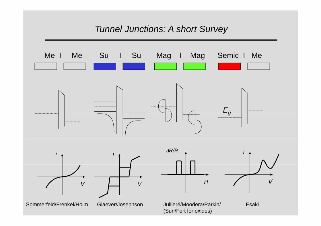
Tunnel Junctions: A short Survey
Me I Me Su I Su Mag I Mag Semic I Me
Egg
I IΔR/R I
V V H V
Sommerfeld/Frenkel/Holm Giaever/Josephson Jullieré/Moodera/Parkin/(Sun/Fert for oxides)
Esaki
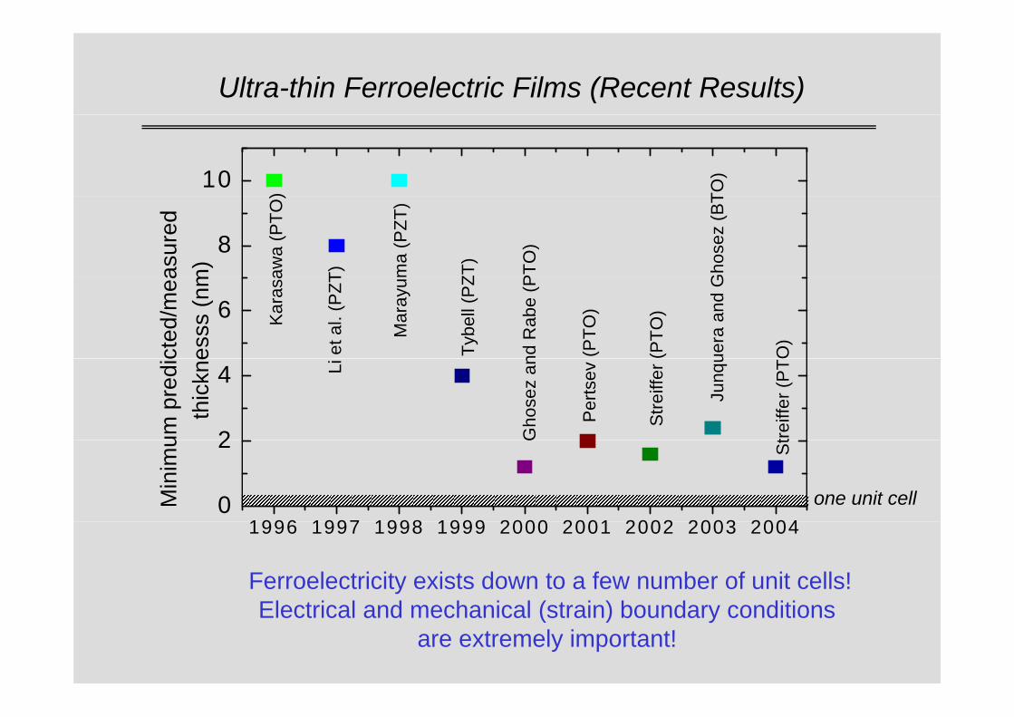
Ultra-thin Ferroelectric Films (Recent Results)
10
TO)
)
8
Gho
sez
(BT
ma
(PZT
)
ZT)
PTO
)
T)awa
(PTO
)
asur
ed
m)
6
O)
uera
and
G
(PTO
)
Mar
ayu
(PTO
)
Tybe
ll (P
Z
nd R
abe
(P
et a
l. (P
ZT
Kar
asa
cted
/mea
esss
(nm
2
4
treiff
er (P
T
Junq
u
Stre
iffer
Per
tsev
Gho
sez
anLi
um p
redi
c
thic
kne
1996 1997 1998 1999 2000 2001 2002 2003 20040
2 StG
Min
imu
one unit cell
Ferroelectricity exists down to a few number of unit cells!El t i l d h i l ( t i ) b d diti
1996 1997 1998 1999 2000 2001 2002 2003 2004
Electrical and mechanical (strain) boundary conditions are extremely important!
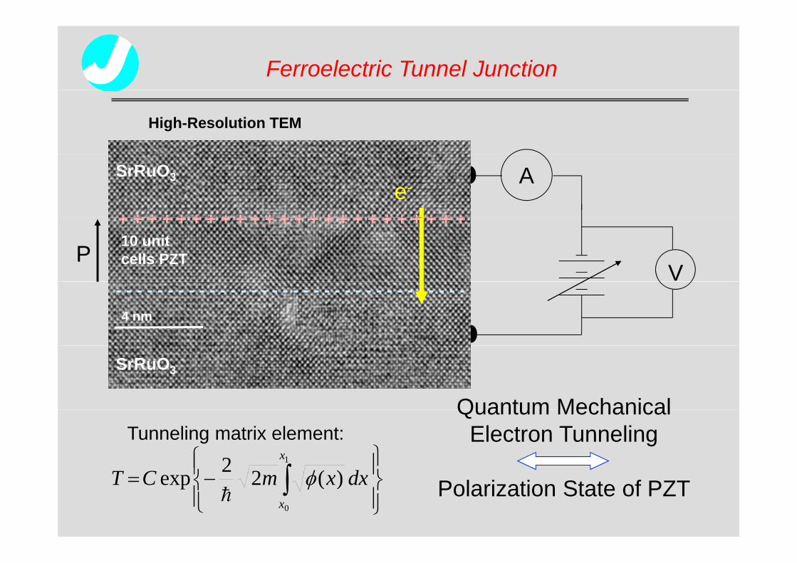
Ferroelectric Tunnel Junction
High-Resolution TEM
ASrRuO3
+ + + + + + + + + + + + + + + + + + + + + + + +e-
V10 unit cells PZT
+ + + + + + + + + + + + + + + + + + + + + + + +
P
4 nm
- - - - - - - - - - - - - - - - - - - - - - - - - - - - - - - - - -
SrRuO3
Quantum Mechanical
⎪⎬⎫⎪
⎨⎧
∫ dCTx1
)(22 φ
Quantum Mechanical Electron TunnelingTunneling matrix element:
⎪⎭
⎪⎬
⎪⎩
⎪⎨−= ∫ dxxmCT
x0
)(2exp φh Polarization State of PZT
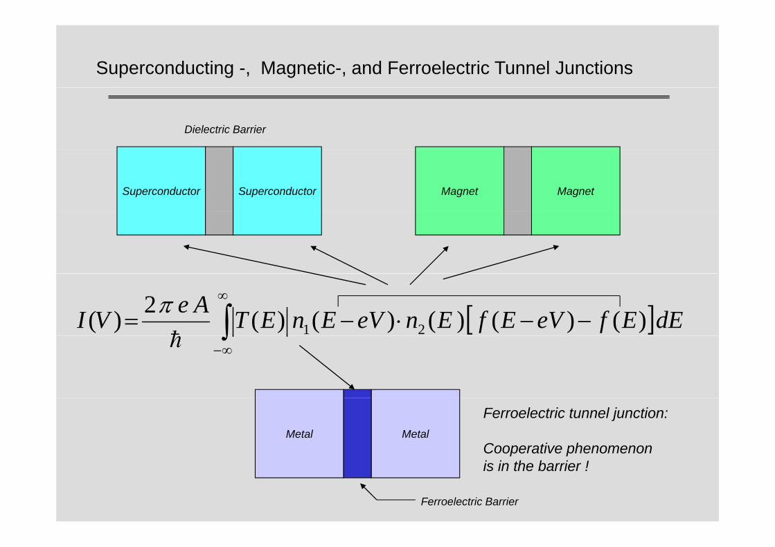
Superconducting -, Magnetic-, and Ferroelectric Tunnel Junctions
Dielectric Barrier
Superconductor Superconductor Magnet Magnet
[ ]dEEfeVEfEneVEnETAeVI )()()()()(2)( 21 −−⋅−= ∫∞
h
π∫∞−h
Metal Metal
Ferroelectric tunnel junction:
Cooperative phenomenon
Ferroelectric Barrier
is in the barrier !
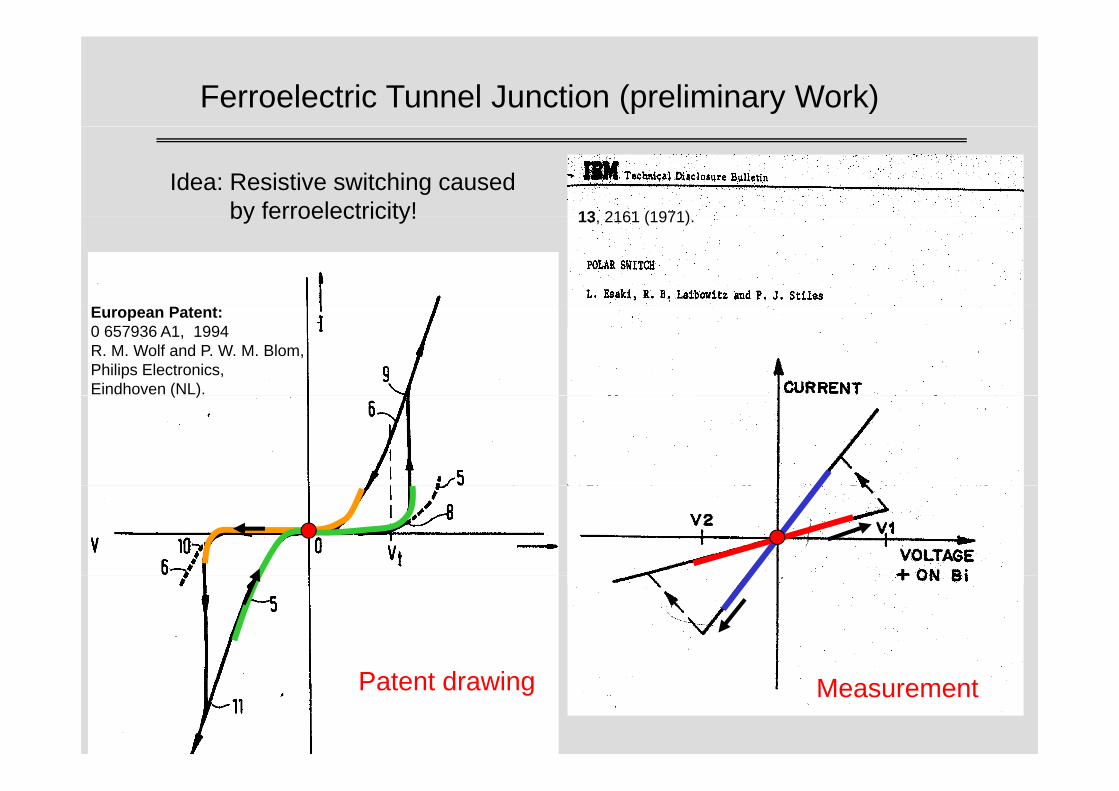
Ferroelectric Tunnel Junction (preliminary Work)
13 2161 (1971)
Idea: Resistive switching caused by ferroelectricity! 13, 2161 (1971).by ferroelectricity!
European Patent:0 657936 A1, 1994R. M. Wolf and P. W. M. Blom, Philips Electronics, Eindhoven (NL).( )
Patent drawing Measurement
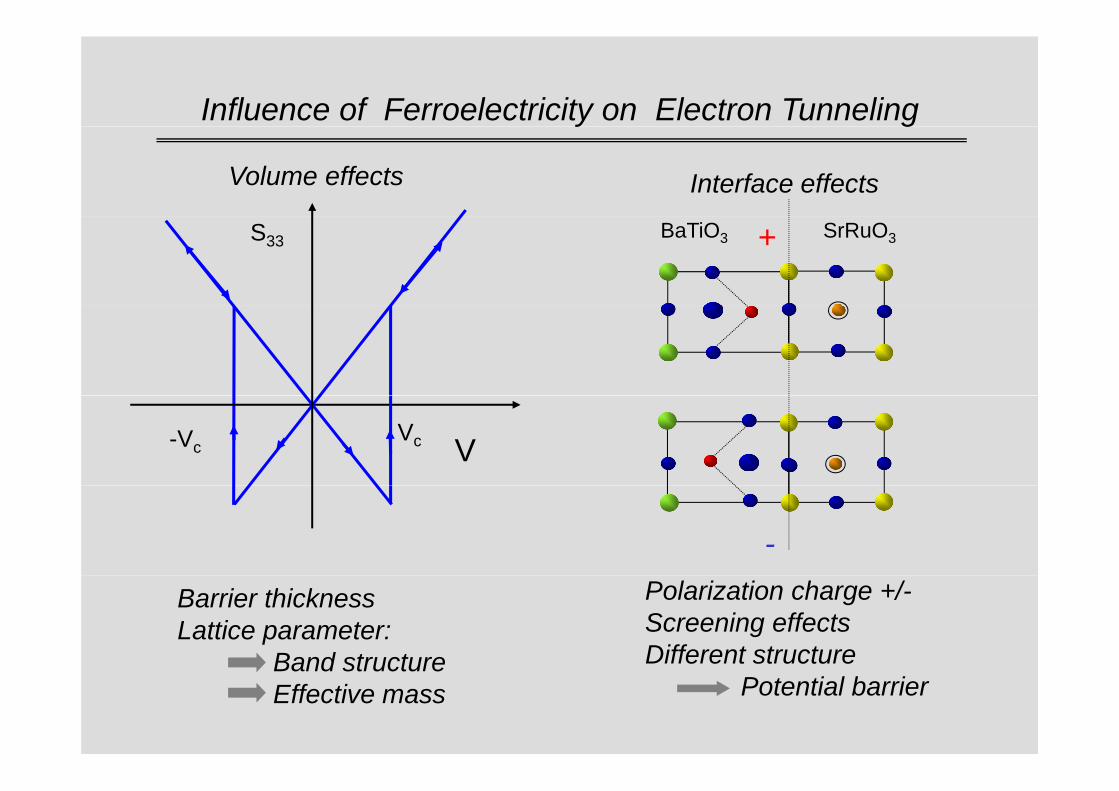
Influence of Ferroelectricity on Electron Tunneling y g
Volume effects Interface effects
S33 SrRuO3BaTiO3 +
VVc-Vc
-
Barrier thicknessLattice parameter:
Band structure
Polarization charge +/-Screening effectsDifferent structureBand structure
Effective mass Potential barrier
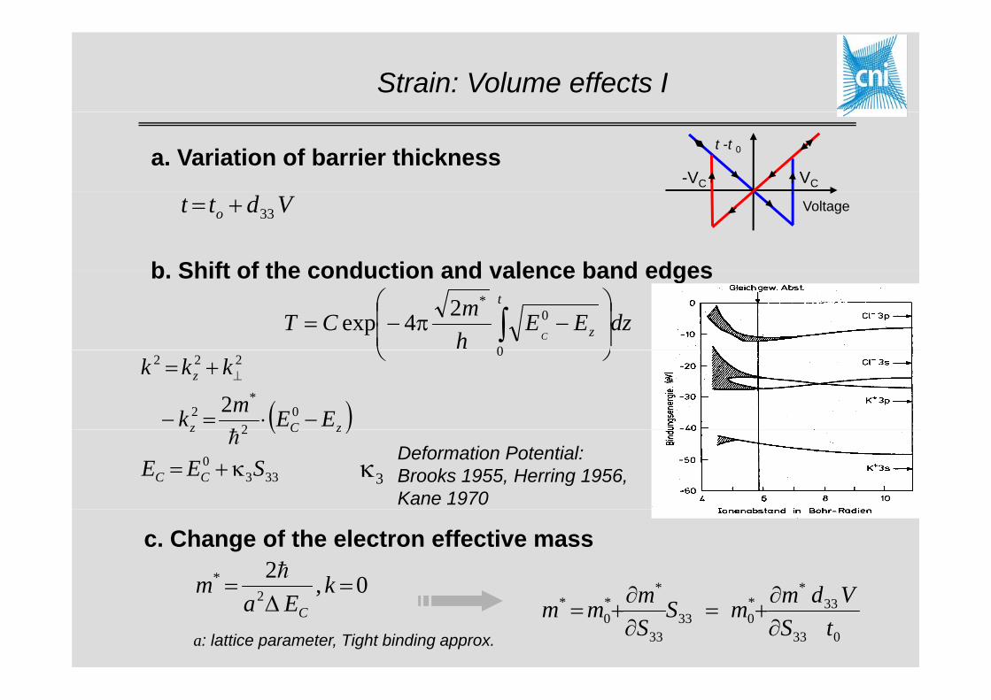
Strain: Volume effects I
t -t 0
VC-VC
a. Variation of barrier thickness
Voltage
b Shift of the conduction and valence band edges
Vdtt o 33+=
b. Shift of the conduction and valence band edges
dzEEhmCT
t
zC ⎟⎟⎠
⎞⎜⎜⎝
⎛−π−= ∫
0
0*24exp
( )02
*2
222
2 EEmk
kkk
zCz
z
−⋅=−
+= ⊥
h
⎠⎝ 0
( )333
0
2
SEE CC
zCz
κ+=h
Deformation Potential:Brooks 1955, Herring 1956, Kane 1970
3κ
c. Change of the electron effective mass
02* == km h** Vd∂∂
a: lattice parameter, Tight binding approx.
0,2 =Δ
= kEa
mC
0
33
33
*033
33
*0
*
tVd
SmmS
Smmm
∂∂
+=∂∂
+=
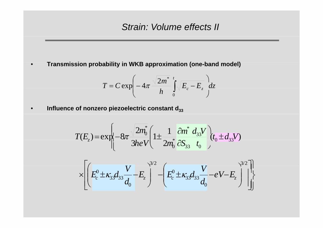
Strain: Volume effects II
T i i b bilit i WKB i ti ( b d d l)• Transmission probability in WKB approximation (one-band model)
dzEEmCTt
zc ⎟⎟⎞
⎜⎜⎛
−−= ∫*24exp π
• Influence of nonzero piezoelectric constant d33
hC zc ⎟
⎠⎜⎝
∫0
p π
⎪
⎪⎨⎧
±⎟⎟⎞
⎜⎜⎛
∂∂
±−= )(112
8exp)( 33033
*
*
*0 VdtVdm
hm
ET z π⎪⎩⎨ ⎟
⎠⎜⎝ ∂
)(23
p)( 330033
*0 tSmheVz
⎪⎫⎤⎡ ⎞⎛⎞⎛2/32/3
VV
⎪⎭
⎪⎬⎫
⎥⎥⎦
⎤
⎢⎢⎣
⎡⎟⎟⎠
⎞⎜⎜⎝
⎛−−±−⎟⎟
⎠
⎞⎜⎜⎝
⎛−±×
03333
0
03333
0zczc EeV
dVdEE
dVdE κκ
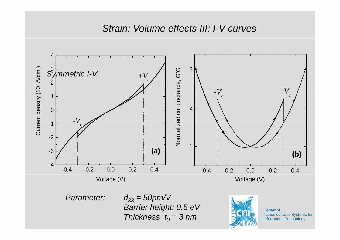
Strain: Volume effects III: I-V curves
4
2
3+Vc
106 A
/cm
2 ) 3
-V +Vance
, G/G
0
Symmetric I-V
0
1
Vnt d
ensi
ty (
2
-Vc+Vc
d co
nduc
ta
-2
-1 -Vc
Cur
ren
1Nor
mal
ize
-0.4 -0.2 0.0 0.2 0.4-4
-3 (a)
-0.4 -0.2 0.0 0.2 0.4
1(b)
Voltage (V) Voltage (V)
Parameter: d33 = 50pm/VCenter ofNanoelectronic Systems forInformation Technology
33 pBarrier height: 0.5 eVThickness t0 = 3 nm
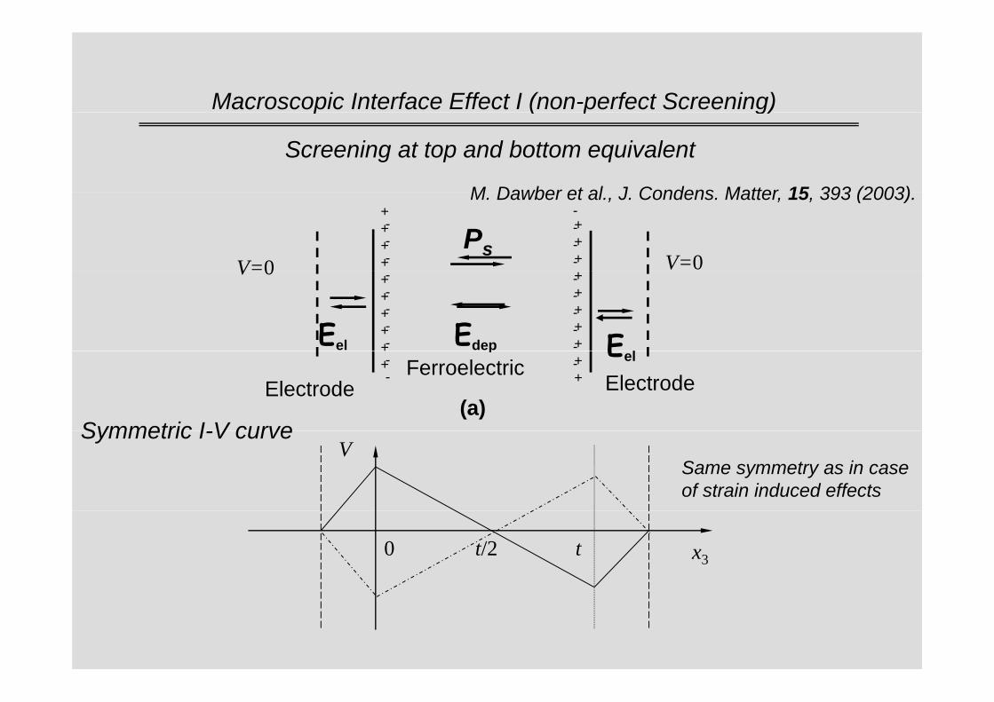
Macroscopic Interface Effect I (non-perfect Screening)p ( p g)
Screening at top and bottom equivalent
M Dawber et al J Condens Matter 15 393 (2003)
PsV=0 V=0
----
++++
---
+++
M. Dawber et al., J. Condens. Matter, 15, 393 (2003).
Edep
V 0
Eel E l
-----
+++++
-----
+++++
Ferroelectricp
Electrode Electrode(a)
Eel-+--
++
Symmetric I V curveV
Same symmetry as in case of strain induced effects
Symmetric I-V curve
0 t/2 t x3
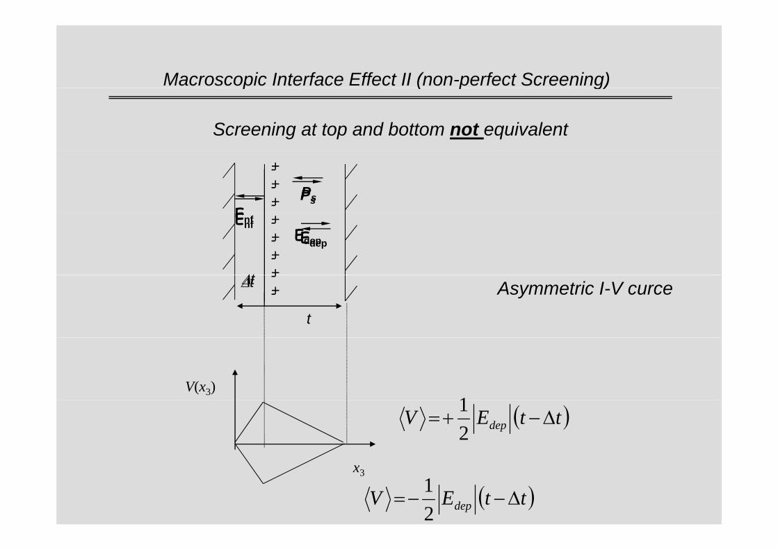
Macroscopic Interface Effect II (non-perfect Screening)p ( p g)
Screening at top and bottom not equivalent
Ps
---
Ps
+++
EEnfEdep
---
Edep
++++Δt
Enf
t
--
Δt ++
Δt Asymmetric I-V curce
V(x3)1 ( )ttEV dep Δ−+=21
x3
( )ttEV dep Δ−−=21
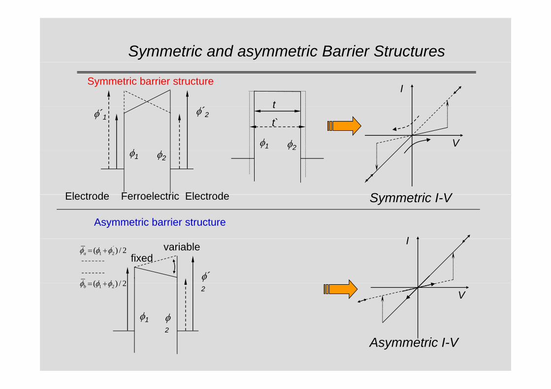
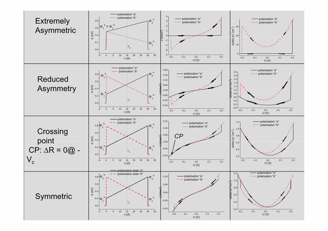
Symmetric and asymmetric Barrier Structures
tI
Symmetric barrier structure
φ
φ´1φ´2
φ1 φ2
t
t`
Vφ1 φ2
Electrode Ferroelectric Electrode S t i I VElectrode Ferroelectric Electrode
I
Asymmetric barrier structure
Symmetric I-V
I
φ´
2/)( ´21 φφφ +=a
2/)( φφφ +
fixedvariable
V
φ1 φ
22/)( 21 φφφ +=b
2
Asymmetric I-V
0.4
0.6
0.8 Φ2a
Φ1a = Φ1
b
(eV)
polarisation "a" polarisation "b"
0
1
2
3
4
A/cm
2 )
polarisation "a" polarisation "b"
20
30
(Ω-1cm
-1)
polarisation "a" polarisation "b"Extremely
Asymmetric
-5 0 5 10 15 20 25 30 35
0.0
0.2
Ym
Φ1b
Φ
x (A) -0.2 -0.1 0.0 0.1 0.2-4
-3
-2
-1J (A
U (V)-0.2 -0.1 0.0 0.1 0.2
0
10dJ/d
U (
U (V)
0.4
0.6
0.8 Φ2a
Φ1b
eV)
polarisation "a" polarisation "b"
0 00
0.05
0.10
0.15
0.20
/cm
2 )
polarisation "a" polarisation "b"
1 01.21.41.61.82.0
(Ω-1cm
-1)
polarisation "a" polarisation "b"
Reduced Asymmetry
-5 0 5 10 15 20 25 30 35
0.0
0.2
0.4
Ym
Φ2bΦ1
aΦ (
x (A) -0.2 -0.1 0.0 0.1 0.2
-0.15
-0.10
-0.05
0.00
J (A
/
U (V)-0.2 -0.1 0.0 0.1 0.2
0.00.20.40.60.81.0
dJ/d
U (
U (V)
Asymmetry
0.4
0.6
0.8 Φ2aΦ1
b
(eV)
polarisation "a" polarisation "b"
0 00
0.05
0.10
0.15
A/cm
2 )
polarisation "a" polarisation "b"
0 6
0.8
1.0
1.2
U (Ω
-1cm
-1)
polarisation "a" polarisation "b"
Crossingpoint CP
-5 0 5 10 15 20 25 30 35
0.0
0.2
Ym
Φ1bΦ1
a
Φ
x (A) -0.2 -0.1 0.0 0.1 0.2
-0.10
-0.05
0.00
J (A
U (V)
-0.2 -0.1 0.0 0.1 0.2
0.2
0.4
0.6
dJ/d
U
U (V)
pointCP: ΔR = 0@ -Vc
0.4
0.6
0.8 Φ2aΦ1
b
Φ (e
V)
polarisation state "a" polarisation state "b"
0.00
0.05
0.10
A/cm
2 )
polarisation "a" polarisation "b"
0 6
0.8
1.0
1.2
dU (Ω
-1cm
-1)
polarisation "a" polarisation "b"
S t i-5 0 5 10 15 20 25 30 35
0.0
0.2
Ym
Φ1bΦ1
a
Φ
x (A) -0.2 -0.1 0.0 0.1 0.2
-0.10
-0.05
J (A
U (V)
-0.2 -0.1 0.0 0.1 0.20.2
0.4
0.6
dJ/d
U (V)
Symmetric
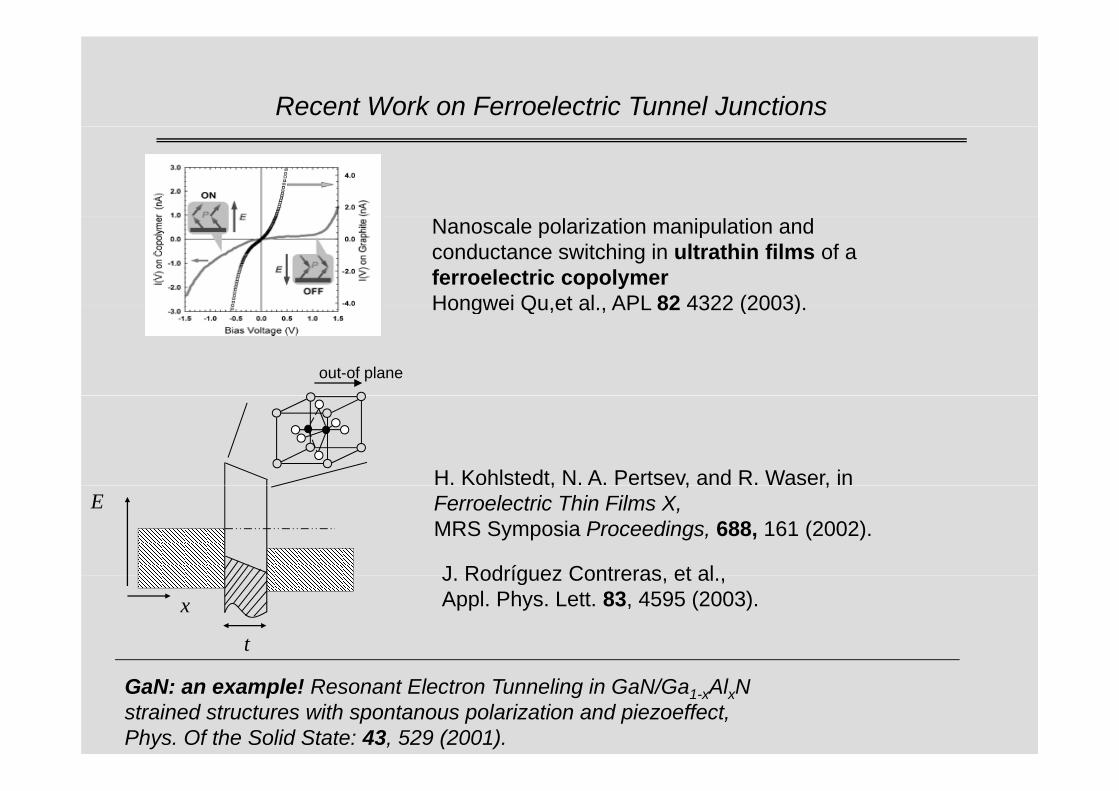
Recent Work on Ferroelectric Tunnel Junctions
Nanoscale polarization manipulation and conductance switching in ultrathin films of a ferroelectric copolymerHongwei Qu et al APL 82 4322 (2003)Hongwei Qu,et al., APL 82 4322 (2003).
out-of plane
H. Kohlstedt, N. A. Pertsev, and R. Waser, in
J Rodríguez Contreras et al
, , ,Ferroelectric Thin Films X, MRS Symposia Proceedings, 688, 161 (2002).
E
J. Rodríguez Contreras, et al.,Appl. Phys. Lett. 83, 4595 (2003).x
t
GaN: an example! Resonant Electron Tunneling in GaN/Ga1-xAlxN strained structures with spontanous polarization and piezoeffect, Phys. Of the Solid State: 43, 529 (2001).

Outlook
Experimental realization of an FTJ p
S d t / S d t / New device structuresSuperconductor/Magnet
Superconductor/Magnet
New device structures
Ferroelectric Barrier
(IETS) Inelastic electron tunneling spectrocopy to study:(IETS)- Inelastic electron tunneling spectrocopy to study:
(1) Domain structures in nm thin ferroelectric materialsor(2) Phonon spectra in ultrathin ferroelectric barriers
AcknowledgementAcknowledgement
The work was supported by the HGF-Strategiefonds “Piccolo” and the V lk F d ti P j tVolkswagen-Foundation--Project
“Nano-sized ferroelectric hybrids” under contract number I/77 737.
DFG Project: „Displacive and Conductive Phenomena in Ferroelectric Thin Films:Scaling effects and switching properties“.
Center ofNanoelectronic Systems forInformation Technologygy
Top Related
