Ferroelectric Tunnel Junctions: A Theoretical Approach · Forschungszentrum Jülich Ferroelectric...
19
Forschungszentrum Jülich Ferroelectric Tunnel Junctions: A Theoretical Approach H. Kohlstedt, A. Petraru, R. Waser Forschungszentrum Jülich GmbH, Institut für Festkörperforschung and CNI, the Center of Nanoelectronic Systems and Information Technology, Germany N. A. Pertsev A. F. Ioffe Physico-Technical Institute, St. Petersburg, Russia Center of Nanoelectronic Systems Information Technology
Transcript of Ferroelectric Tunnel Junctions: A Theoretical Approach · Forschungszentrum Jülich Ferroelectric...
Forschungszentrum Jülich
Ferroelectric Tunnel Junctions: A Theoretical Approach
H. Kohlstedt, A. Petraru, R. WaserForschungszentrum Jülich GmbH,
Institut für Festkörperforschung and CNI, the Center of Nanoelectronic Systems and Information Technology, Germany
N. A. PertsevA. F. Ioffe Physico-Technical Institute, St. Petersburg, Russia
Center ofNanoelectronic Systems Information Technology
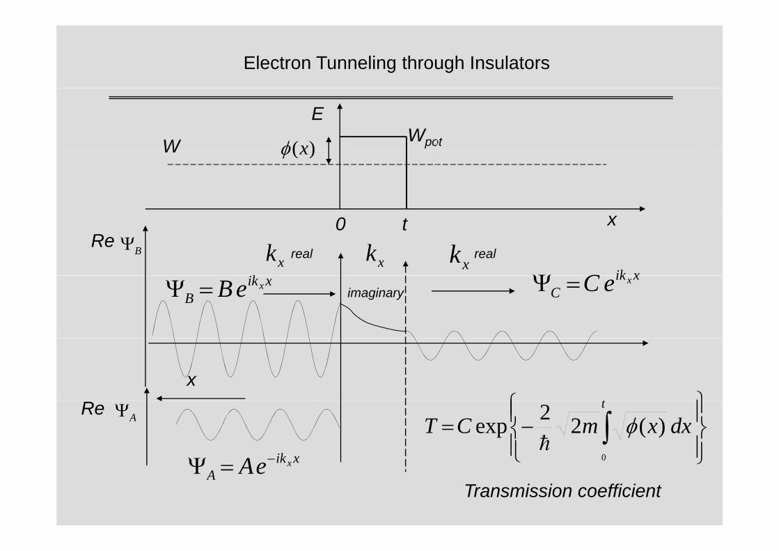
Electron Tunneling through Insulators
EWpotW )(xφW )(xφ
xt0
k xikCΨxk real xk xk real
Re BΨ
xikB
xeB=Ψxik
CxeC=Ψimaginary
x
⎪⎫⎪⎧ t
xikxA −Ψ
Re AΨ
⎪⎭
⎪⎬⎫
⎪⎩
⎪⎨⎧−= ∫ dxxmCT
t
0
)(22exp φh
AxeA=Ψ ⎭
Transmission coefficient
Electron tunneling: Current Transport Equation
Metal 1 Metal 2I
Fermi distributions of(occupied/unoccupied) states
Fermi distributions of( i d/ i d) t tj
j2-1(occupied/unoccupied) states
+ eVT
j1-2
dd
−− −=−=
jjjdirectionxdensitycurrentnvej x
1221
:
[ ] ⊥⊥
∞
⋅−= ∫∫⊥
⊥dkkTEfEfdEej
k
kE
max)(
),(213 )()(4 hπ o 04 hπ
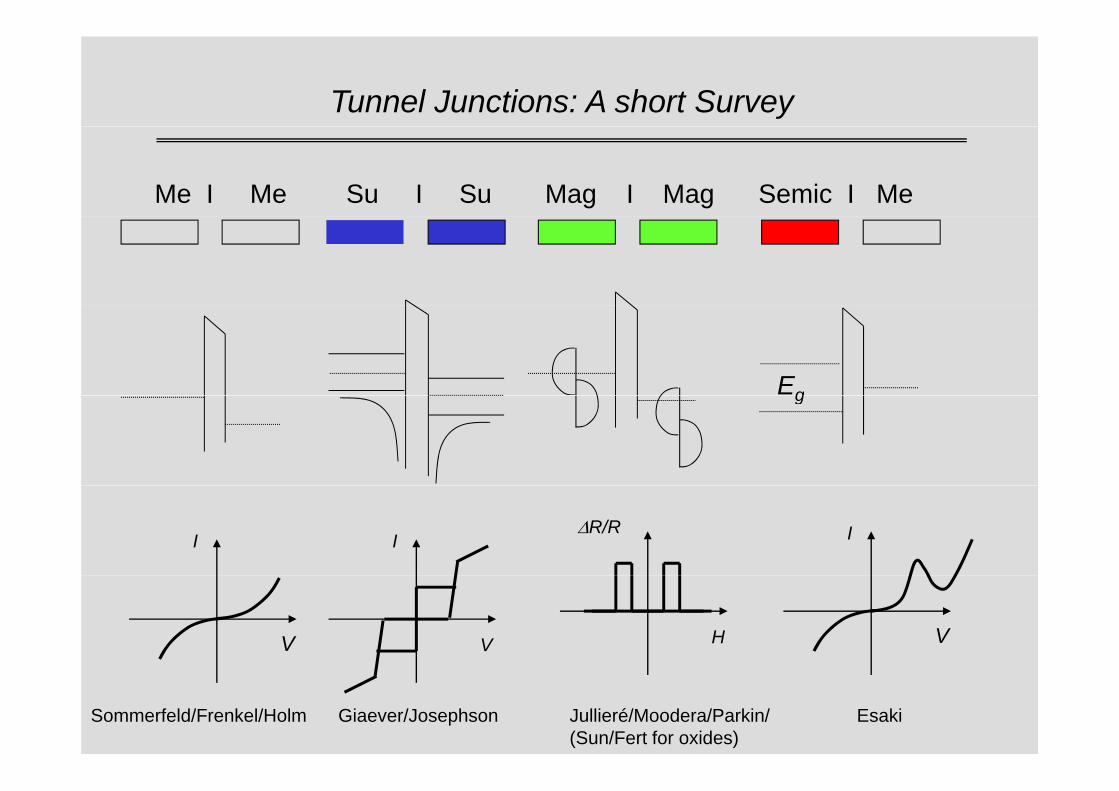
Tunnel Junctions: A short Survey
Me I Me Su I Su Mag I Mag Semic I Me
Egg
I IΔR/R I
V V H V
Sommerfeld/Frenkel/Holm Giaever/Josephson Jullieré/Moodera/Parkin/(Sun/Fert for oxides)
Esaki
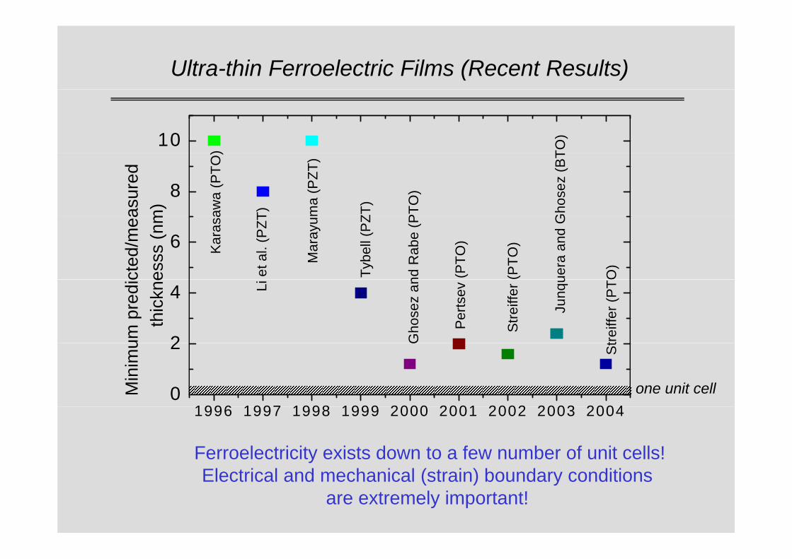
Ultra-thin Ferroelectric Films (Recent Results)
10
TO)
)
8
Gho
sez
(BT
ma
(PZT
)
ZT)
PTO
)
T)awa
(PTO
)
asur
ed
m)
6
O)
uera
and
G
(PTO
)
Mar
ayu
(PTO
)
Tybe
ll (P
Z
nd R
abe
(P
et a
l. (P
ZT
Kar
asa
cted
/mea
esss
(nm
2
4
treiff
er (P
T
Junq
u
Stre
iffer
Per
tsev
Gho
sez
anLi
um p
redi
c
thic
kne
1996 1997 1998 1999 2000 2001 2002 2003 20040
2 StG
Min
imu
one unit cell
Ferroelectricity exists down to a few number of unit cells!El t i l d h i l ( t i ) b d diti
1996 1997 1998 1999 2000 2001 2002 2003 2004
Electrical and mechanical (strain) boundary conditions are extremely important!
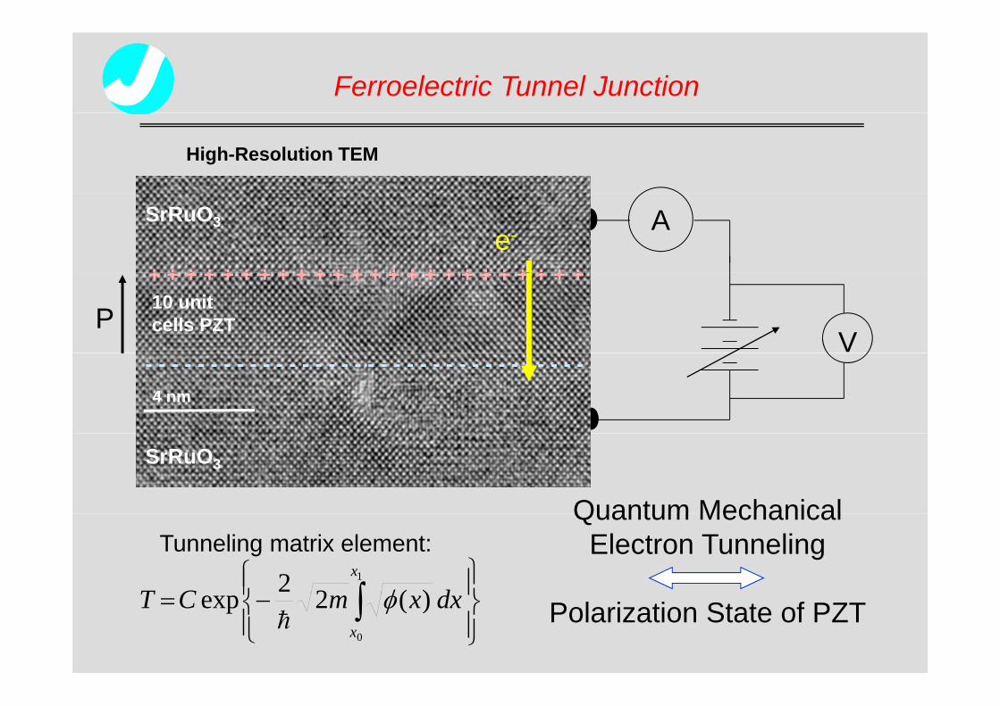
Ferroelectric Tunnel Junction
High-Resolution TEM
ASrRuO3
+ + + + + + + + + + + + + + + + + + + + + + + +e-
V10 unit cells PZT
+ + + + + + + + + + + + + + + + + + + + + + + +
P
4 nm
- - - - - - - - - - - - - - - - - - - - - - - - - - - - - - - - - -
SrRuO3
Quantum Mechanical
⎪⎬⎫⎪
⎨⎧
∫ dCTx1
)(22 φ
Quantum Mechanical Electron TunnelingTunneling matrix element:
⎪⎭
⎪⎬
⎪⎩
⎪⎨−= ∫ dxxmCT
x0
)(2exp φh Polarization State of PZT
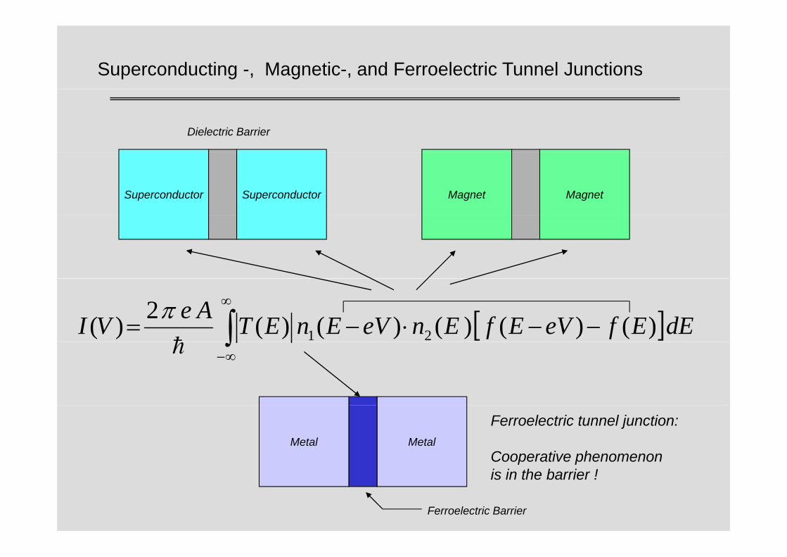
Superconducting -, Magnetic-, and Ferroelectric Tunnel Junctions
Dielectric Barrier
Superconductor Superconductor Magnet Magnet
[ ]dEEfeVEfEneVEnETAeVI )()()()()(2)( 21 −−⋅−= ∫∞
h
π∫∞−h
Metal Metal
Ferroelectric tunnel junction:
Cooperative phenomenon
Ferroelectric Barrier
is in the barrier !
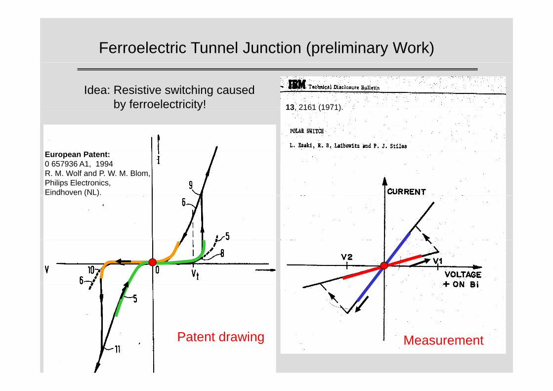
Ferroelectric Tunnel Junction (preliminary Work)
13 2161 (1971)
Idea: Resistive switching caused by ferroelectricity! 13, 2161 (1971).by ferroelectricity!
European Patent:0 657936 A1, 1994R. M. Wolf and P. W. M. Blom, Philips Electronics, Eindhoven (NL).( )
Patent drawing Measurement
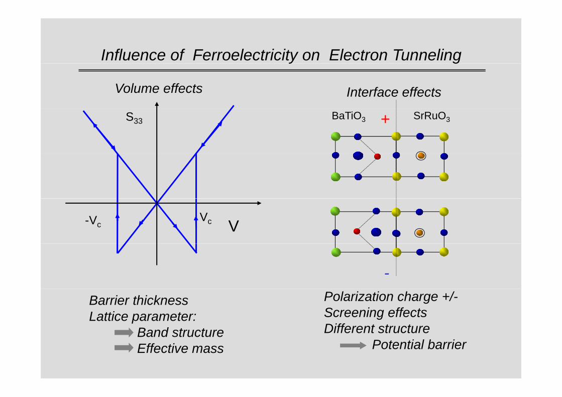
Influence of Ferroelectricity on Electron Tunneling y g
Volume effects Interface effects
S33 SrRuO3BaTiO3 +
VVc-Vc
-
Barrier thicknessLattice parameter:
Band structure
Polarization charge +/-Screening effectsDifferent structureBand structure
Effective mass Potential barrier
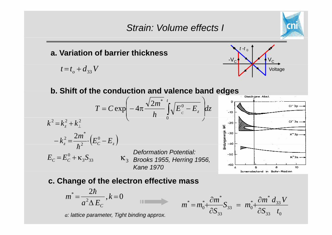
Strain: Volume effects I
t -t 0
VC-VC
a. Variation of barrier thickness
Voltage
b Shift of the conduction and valence band edges
Vdtt o 33+=
b. Shift of the conduction and valence band edges
dzEEhmCT
t
zC ⎟⎟⎠
⎞⎜⎜⎝
⎛−π−= ∫
0
0*24exp
( )02
*2
222
2 EEmk
kkk
zCz
z
−⋅=−
+= ⊥
h
⎠⎝ 0
( )333
0
2
SEE CC
zCz
κ+=h
Deformation Potential:Brooks 1955, Herring 1956, Kane 1970
3κ
c. Change of the electron effective mass
02* == km h** Vd∂∂
a: lattice parameter, Tight binding approx.
0,2 =Δ
= kEa
mC
0
33
33
*033
33
*0
*
tVd
SmmS
Smmm
∂∂
+=∂∂
+=
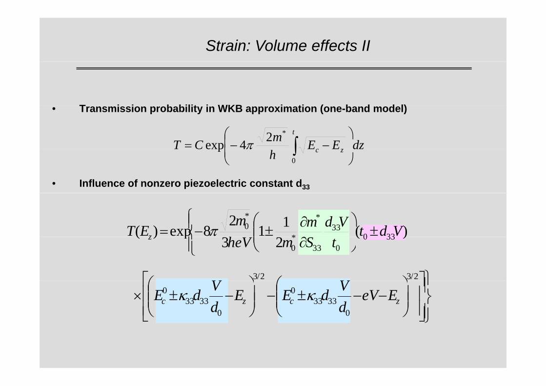
Strain: Volume effects II
T i i b bilit i WKB i ti ( b d d l)• Transmission probability in WKB approximation (one-band model)
dzEEmCTt
zc ⎟⎟⎞
⎜⎜⎛
−−= ∫*24exp π
• Influence of nonzero piezoelectric constant d33
hC zc ⎟
⎠⎜⎝
∫0
p π
⎪
⎪⎨⎧
±⎟⎟⎞
⎜⎜⎛
∂∂
±−= )(112
8exp)( 33033
*
*
*0 VdtVdm
hm
ET z π⎪⎩⎨ ⎟
⎠⎜⎝ ∂
)(23
p)( 330033
*0 tSmheVz
⎪⎫⎤⎡ ⎞⎛⎞⎛2/32/3
VV
⎪⎭
⎪⎬⎫
⎥⎥⎦
⎤
⎢⎢⎣
⎡⎟⎟⎠
⎞⎜⎜⎝
⎛−−±−⎟⎟
⎠
⎞⎜⎜⎝
⎛−±×
03333
0
03333
0zczc EeV
dVdEE
dVdE κκ
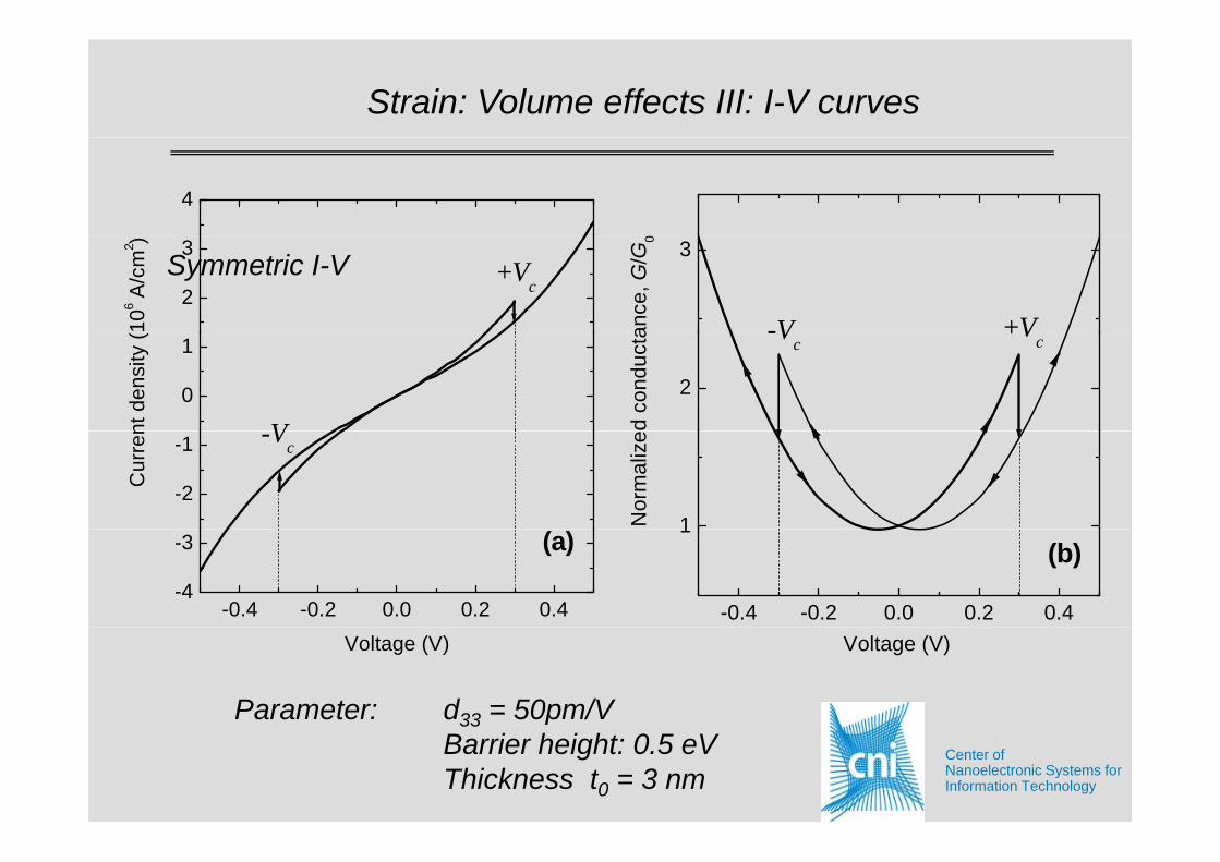
Strain: Volume effects III: I-V curves
4
2
3+Vc
106 A
/cm
2 ) 3
-V +Vance
, G/G
0
Symmetric I-V
0
1
Vnt d
ensi
ty (
2
-Vc+Vc
d co
nduc
ta
-2
-1 -Vc
Cur
ren
1Nor
mal
ize
-0.4 -0.2 0.0 0.2 0.4-4
-3 (a)
-0.4 -0.2 0.0 0.2 0.4
1(b)
Voltage (V) Voltage (V)
Parameter: d33 = 50pm/VCenter ofNanoelectronic Systems forInformation Technology
33 pBarrier height: 0.5 eVThickness t0 = 3 nm
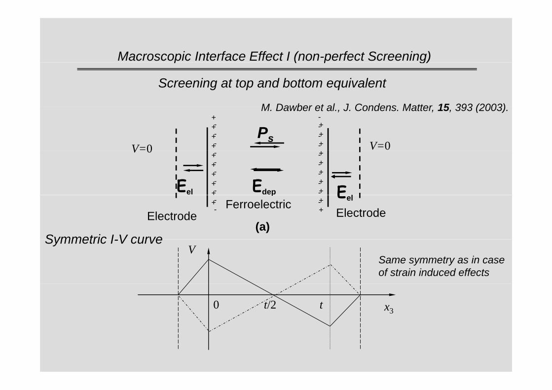
Macroscopic Interface Effect I (non-perfect Screening)p ( p g)
Screening at top and bottom equivalent
M Dawber et al J Condens Matter 15 393 (2003)
PsV=0 V=0
----
++++
---
+++
M. Dawber et al., J. Condens. Matter, 15, 393 (2003).
Edep
V 0
Eel E l
-----
+++++
-----
+++++
Ferroelectricp
Electrode Electrode(a)
Eel-+--
++
Symmetric I V curveV
Same symmetry as in case of strain induced effects
Symmetric I-V curve
0 t/2 t x3
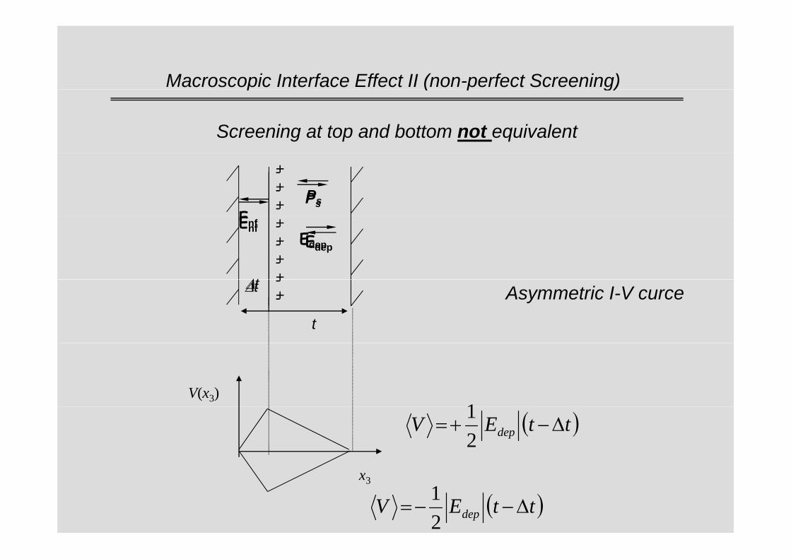
Macroscopic Interface Effect II (non-perfect Screening)p ( p g)
Screening at top and bottom not equivalent
Ps
---
Ps
+++
EEnfEdep
---
Edep
++++Δt
Enf
t
--
Δt ++
Δt Asymmetric I-V curce
V(x3)1 ( )ttEV dep Δ−+=21
x3
( )ttEV dep Δ−−=21
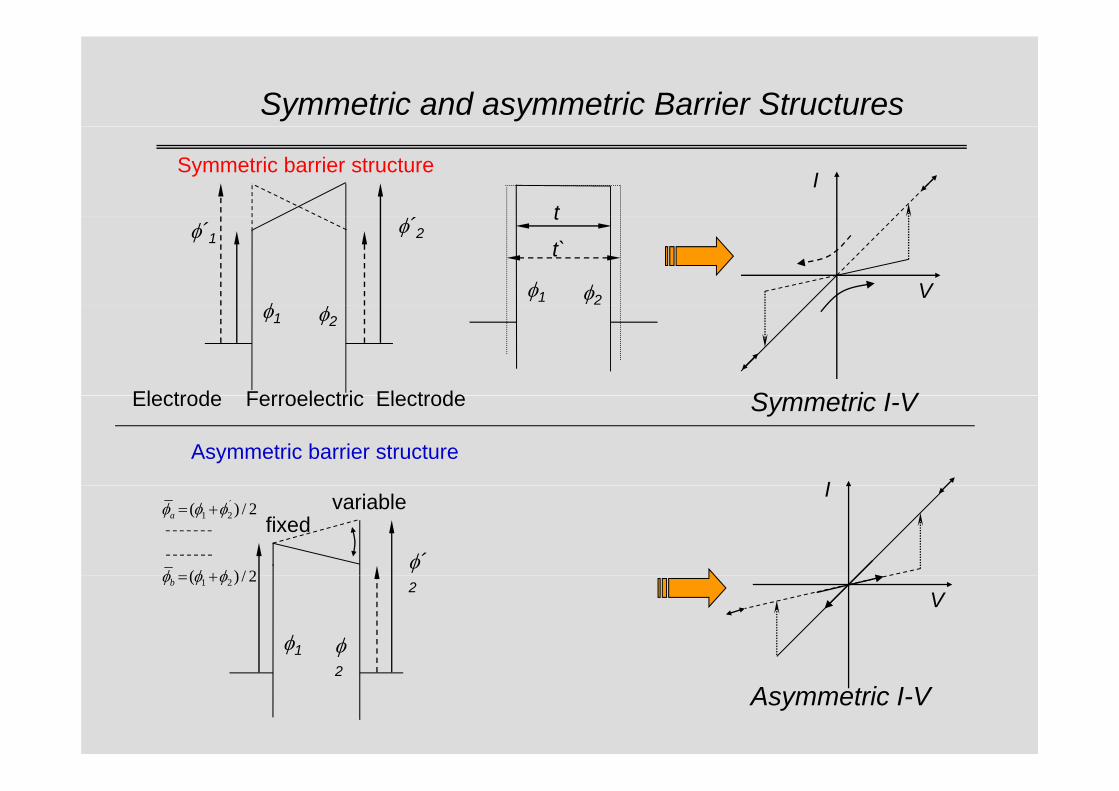
Symmetric and asymmetric Barrier Structures
tI
Symmetric barrier structure
φ
φ´1φ´2
φ1 φ2
t
t`
Vφ1 φ2
Electrode Ferroelectric Electrode S t i I VElectrode Ferroelectric Electrode
I
Asymmetric barrier structure
Symmetric I-V
I
φ´
2/)( ´21 φφφ +=a
2/)( φφφ +
fixedvariable
V
φ1 φ
22/)( 21 φφφ +=b
2
Asymmetric I-V
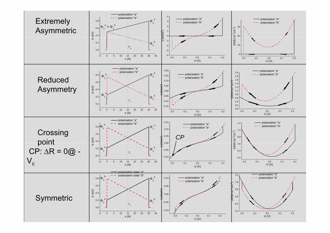
0.4
0.6
0.8 Φ2a
Φ1a = Φ1
b
(eV)
polarisation "a" polarisation "b"
0
1
2
3
4
A/cm
2 )
polarisation "a" polarisation "b"
20
30
(Ω-1cm
-1)
polarisation "a" polarisation "b"Extremely
Asymmetric
-5 0 5 10 15 20 25 30 35
0.0
0.2
Ym
Φ1b
Φ
x (A) -0.2 -0.1 0.0 0.1 0.2-4
-3
-2
-1J (A
U (V)-0.2 -0.1 0.0 0.1 0.2
0
10dJ/d
U (
U (V)
0.4
0.6
0.8 Φ2a
Φ1b
eV)
polarisation "a" polarisation "b"
0 00
0.05
0.10
0.15
0.20
/cm
2 )
polarisation "a" polarisation "b"
1 01.21.41.61.82.0
(Ω-1cm
-1)
polarisation "a" polarisation "b"
Reduced Asymmetry
-5 0 5 10 15 20 25 30 35
0.0
0.2
0.4
Ym
Φ2bΦ1
aΦ (
x (A) -0.2 -0.1 0.0 0.1 0.2
-0.15
-0.10
-0.05
0.00
J (A
/
U (V)-0.2 -0.1 0.0 0.1 0.2
0.00.20.40.60.81.0
dJ/d
U (
U (V)
Asymmetry
0.4
0.6
0.8 Φ2aΦ1
b
(eV)
polarisation "a" polarisation "b"
0 00
0.05
0.10
0.15
A/cm
2 )
polarisation "a" polarisation "b"
0 6
0.8
1.0
1.2
U (Ω
-1cm
-1)
polarisation "a" polarisation "b"
Crossingpoint CP
-5 0 5 10 15 20 25 30 35
0.0
0.2
Ym
Φ1bΦ1
a
Φ
x (A) -0.2 -0.1 0.0 0.1 0.2
-0.10
-0.05
0.00
J (A
U (V)
-0.2 -0.1 0.0 0.1 0.2
0.2
0.4
0.6
dJ/d
U
U (V)
pointCP: ΔR = 0@ -Vc
0.4
0.6
0.8 Φ2aΦ1
b
Φ (e
V)
polarisation state "a" polarisation state "b"
0.00
0.05
0.10
A/cm
2 )
polarisation "a" polarisation "b"
0 6
0.8
1.0
1.2
dU (Ω
-1cm
-1)
polarisation "a" polarisation "b"
S t i-5 0 5 10 15 20 25 30 35
0.0
0.2
Ym
Φ1bΦ1
a
Φ
x (A) -0.2 -0.1 0.0 0.1 0.2
-0.10
-0.05
J (A
U (V)
-0.2 -0.1 0.0 0.1 0.20.2
0.4
0.6
dJ/d
U (V)
Symmetric
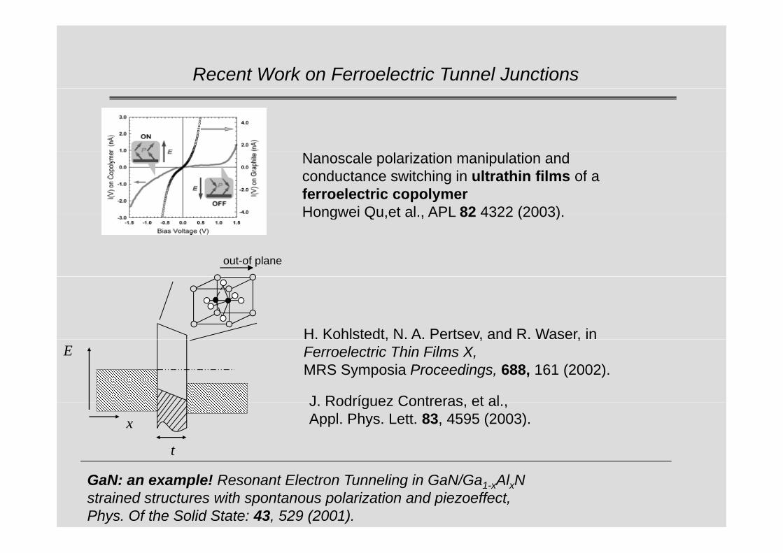
Recent Work on Ferroelectric Tunnel Junctions
Nanoscale polarization manipulation and conductance switching in ultrathin films of a ferroelectric copolymerHongwei Qu et al APL 82 4322 (2003)Hongwei Qu,et al., APL 82 4322 (2003).
out-of plane
H. Kohlstedt, N. A. Pertsev, and R. Waser, in
J Rodríguez Contreras et al
, , ,Ferroelectric Thin Films X, MRS Symposia Proceedings, 688, 161 (2002).
E
J. Rodríguez Contreras, et al.,Appl. Phys. Lett. 83, 4595 (2003).x
t
GaN: an example! Resonant Electron Tunneling in GaN/Ga1-xAlxN strained structures with spontanous polarization and piezoeffect, Phys. Of the Solid State: 43, 529 (2001).

Outlook
Experimental realization of an FTJ p
S d t / S d t / New device structuresSuperconductor/Magnet
Superconductor/Magnet
New device structures
Ferroelectric Barrier
(IETS) Inelastic electron tunneling spectrocopy to study:(IETS)- Inelastic electron tunneling spectrocopy to study:
(1) Domain structures in nm thin ferroelectric materialsor(2) Phonon spectra in ultrathin ferroelectric barriers
AcknowledgementAcknowledgement
The work was supported by the HGF-Strategiefonds “Piccolo” and the V lk F d ti P j tVolkswagen-Foundation--Project
“Nano-sized ferroelectric hybrids” under contract number I/77 737.
DFG Project: „Displacive and Conductive Phenomena in Ferroelectric Thin Films:Scaling effects and switching properties“.
Center ofNanoelectronic Systems forInformation Technologygy


![Sangeetha [Ferroelectric Memory]](https://static.fdocuments.net/doc/165x107/55cf8f91550346703b9d9665/sangeetha-ferroelectric-memory.jpg)