


Languages
Pages
Legal

1
Department of Electrical Engineering
NIT Rourkela
Design and Implementation of ZCS Buck Converter
Project Report for Final Evaluation
Submitted by:
Gyana Ranjan Sahu(10602019)
Bimal Prasad Behera(10602044)
Rohit Dash ( 10602043)
Guided by:
Prof. A.K. Panda
Signature of the guide:
2
CERTIFICATE This is to certify that the thesis titled – “Design and Implementation of a
Zero Current Switched Buck Converter” submitted by Sri Gyana
Ranjan Sahu, Sri Rohit Dash and Sri Bimal Prasad Behera in partial
fulfillment of the requirements for the award of Bachelor of Technology Degree
in Electrical Engineering at the National Institute of Technology, Rourkela
(Deemed University) is an authentic work carried out by them under my
guidance and supervision. The matter embodied in the thesis has not been
submitted to or published in any other University / Institute for the award of any
Degree or Diploma to the best of my knowledge and belief.
Date: 08/05/10 Prof. A.K.Panda
Department of Electrical Engg.
National Institute of Technology
Rourkela - 769008
3
ACKNOWLEDGEMENT
We would like to begin by thanking Prof. A. K. Panda for his efforts and
endeavour in guiding and helping us for our Project work and also we express
our heartfelt gratitude towards all our dept. staffs in Lab who have contributed
their precious time to help us in completing our project. We are also grateful to
Head of the Electrical Engineering Department Prof. B. D. Subudhi for
providing necessary facilities in the department. We are also indebted to Power
Electronics Lab and Assistant Sanyasi Babu for providing valuable
troubleshooting inputs. An assemblage of this nature could never have been
attempted without reference to and inspiration from the works of others whose
details are mentioned in reference section. We acknowledge our indebtedness to
all of them.
Date : 08/05/10 Gyana Ranjan Sahu
Rohit Dash
Bimal Prasad Behera
4
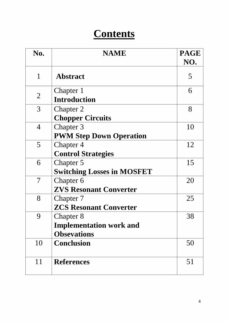
Contents
No. NAME PAGE
NO.
1
Abstract
5
2 Chapter 1
Introduction
6
3 Chapter 2
Chopper Circuits
8
4 Chapter 3
PWM Step Down Operation
10
5 Chapter 4
Control Strategies
12
6 Chapter 5
Switching Losses in MOSFET
15
7 Chapter 6
ZVS Resonant Converter
20
8 Chapter 7
ZCS Resonant Converter
25
9 Chapter 8
Implementation work and
Obsevations
38
10 Conclusion 50
11 References 51
5
Abstract
Buck converters are step-down DC-DC converters that are
widely being used in different electronic devices like laptops,PDA’s,cell phones and also
electric vehicles to obtain different level of voltages. These converters are nothing but ,high
frequency switching devices operating on PWM principle. The need for more and more
lighter and smaller electronic devices propels the need for reduced size of converters
operating at higher load currents. With all these inadvertent conditions the switching
frequency has jumped from KHz range to MHz range.The switching devices are made to
turn on and turn off the entire load current at high di/dt , and also withstand high voltage
stress across them.Due to these two effects there occurs increased power losses in these
converters and reduces the efficiency significantly. The reduction in efficiency is highly
unacceptable as it leads to shorter battery life and derated device conditions.
The shortcomings explained above can be minimised and upto some
extent eliminated if each switch is made to turn-on and turn-off when the voltage across it
and/or current through it is zero at the instant of switching. The converter circuits which
employ zero voltage and /or zero current switching are known as Resonant converters. In
most of these converters some form of L-C resonance is used, that is why these are known as
resonant converters.
In this project a detailed study of zero current switching buck converters is
done and also practically implemented in hardware. In addition a mathematical analysis of
switching loss occuring in MOSFET’s is also presented and a short study of zero voltage
switching is also appended. During the hardware implementation the Ton,Toff and operating
frequency were found out and thoroughly tuned through the IC555 circuit and various
waveforms across inductors,capacitors,load resistor and test points were noted down. These
waveforms were found to be in precise proximity of the theoretically observed waveforms.
6
Chapter 1
INTRODUCTION
DC-DC converters are electronic devices that are used to
change DC electrical power efficiently from one voltage level to another. The use of one or
more switches for the purpose of power conversion can be regarded as a SMPS. A few
applications of DC-DC converters are where 5V DC on a personal computer motherboard
must be stepped down to 3V, 2V or less. In all of these applications, we want to change the
DC energy from one voltage level to another, while wasting as little as possible in the
process. In other words, we want to perform the conversion with the highest possible
efficiency. DC-DC Converters are needed because unlike AC, DC can’t simply be stepped up
or down using a transformer. In many ways a DC-DC converter is the DC equivalent of a
transformer. They essentially just change the input energy into a different impedance level.
SWITCHING MODE REGULATORS
DC converters can be used as switching-mode regulators to
convert a dc voltage, normally unregulated to a regulated dc output voltage. The regulation is
achieved by PWM at a fixed frequency and the switching device is normally BJT, MOSFET,
or IGBT. The output of dc converters contains harmonics and the ripple content is normally
reduced by an LC filter.
Switching regulators are commercially available as integrated circuits. The
designer can select the switching frequency by choosing the values of R and C of frequency
oscillator. As a rule of thumb, to maximize efficiency, the minimum oscillator period should
be about 100 times longer than the transistor switching time; for example, if a transistor has a
switching time of 0.5µs, the oscillator period would be 50µs, which gives the maximum
oscillator frequency of 20kHz. This limitation is due a switching loss in transistor. The
transistor switching loss increases with the switching frequency and as a result the efficiency
decreases. In addition, the core loss of inductors limits the high-frequency operation. Control
voltage is obtained by comparing the output voltage with its desired value. The reference

7
voltage can be compared with a saw-tooth voltage to generate the PWM control signal for the
dc converter. There are three basic topologies of switching regulators.
Buck regulators
Boost regulators
Cuk regulators
Furthermore, depending upon the direction of current and
voltage flows, dc converters can be classified into five types:
First quadrant converters
Second quadrant converters
First and second quadrant converters
Third and fourth quadrant converters
Four-quadrant converters
8
Chapter 2
CHOPPER CIRCUITS
Many industrial applications require power from DC sources. Several
of these applications, however, perform better in case these are fed from variable DC
voltage sources. Examples of such DC system are subway cars, trolley buses, battery-
operated vehicles, battery charging etc.
From an AC supply systems, variable DC output voltage can be
obtained through the use of phase controlled converters or motor-generator sets. The
conversion of fixed DC voltage to an adjustable DC output voltage through the use of
semiconductor devices, can be carried out by the use of two types of DC to DC converters
mentioned below.
(1) AC link chopper : In the ac link chopper dc is first converted to ac by an inverter
(dc to ac converter), ac is then stepped-up or stepped-down by a transformer which is
then converted back to a dc by a diode rectifier. As the conversion is in two stages, dc to
ac and then ac to dc, the link chopper is costly, bulky and less efficient.
(a) AC link chopper (b) dc chopper
(c)Representation of power semiconductor device
9
(2) DC Chopper : A chopper is a static device that converts fixed dc input voltage
to a variable dc output voltage directly. A chopper may be thought of as dc equivalent of
an ac transformer since they behave in an identical manner. As choppers involve one
stage conversion, these are more efficient.
Choppers are now being used all over the world for rapid transit
systems. These are also used in trolley cars, marine hoists etc. The future electric
automobiles are likely to use choppers for their speed control and braking. Chopper
systems offer smooth control, high efficiency, fast response and regeneration. The power
semiconductor devices used for a chopper circuit can be force-commutated thyristor,
power BJT, power MOSFET, GTO or IGBT. Like the transformer, a chopper can also be
used to step-down or step-up the fixed input voltage.
10
Chapter 3
PWM STEP DOWN OPERATION
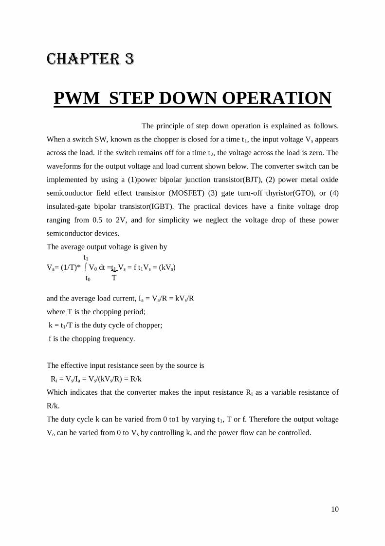
The principle of step down operation is explained as follows.
When a switch SW, known as the chopper is closed for a time t1, the input voltage Vs appears
across the load. If the switch remains off for a time t2, the voltage across the load is zero. The
waveforms for the output voltage and load current shown below. The converter switch can be
implemented by using a (1)power bipolar junction transistor(BJT), (2) power metal oxide
semiconductor field effect transistor (MOSFET) (3) gate turn-off thyristor(GTO), or (4)
insulated-gate bipolar transistor(IGBT). The practical devices have a finite voltage drop
ranging from 0.5 to 2V, and for simplicity we neglect the voltage drop of these power
semiconductor devices.
The average output voltage is given by
t1
Va= (1/T)* ∫ V0 dt =t1 Vs = f t1Vs = (kVs)
t0 T
and the average load current, Ia = Va/R = kVs/R
where T is the chopping period;
k = t1/T is the duty cycle of chopper;
f is the chopping frequency.
The effective input resistance seen by the source is
Ri = Vs/Ia = Vs/(kVs/R) = R/k
Which indicates that the converter makes the input resistance Ri as a variable resistance of
R/k.
The duty cycle k can be varied from 0 to1 by varying t1, T or f. Therefore the output voltage
Vo can be varied from 0 to Vs by controlling k, and the power flow can be controlled.
11
+ t=0 +
SW
Vs V0 R
- -
12
Chapter 4
CONTROL STRATEGIES It is seen that the average value of Output voltage V0 can be controlled through
Duty Cycle D by opening and closing the semiconductor switch periodically. The various
control strategies for varying the duty cycle D are as follows:
1. Time ratio Control (TRC)
2. Current-limit Control
1. Time Ratio Control (TRC) :
As the name suggests, in this control scheme the duty cycle is varied. This is realized in two
different control strategies :
(a) Constant Frequency System
(b) Variable Frequency System
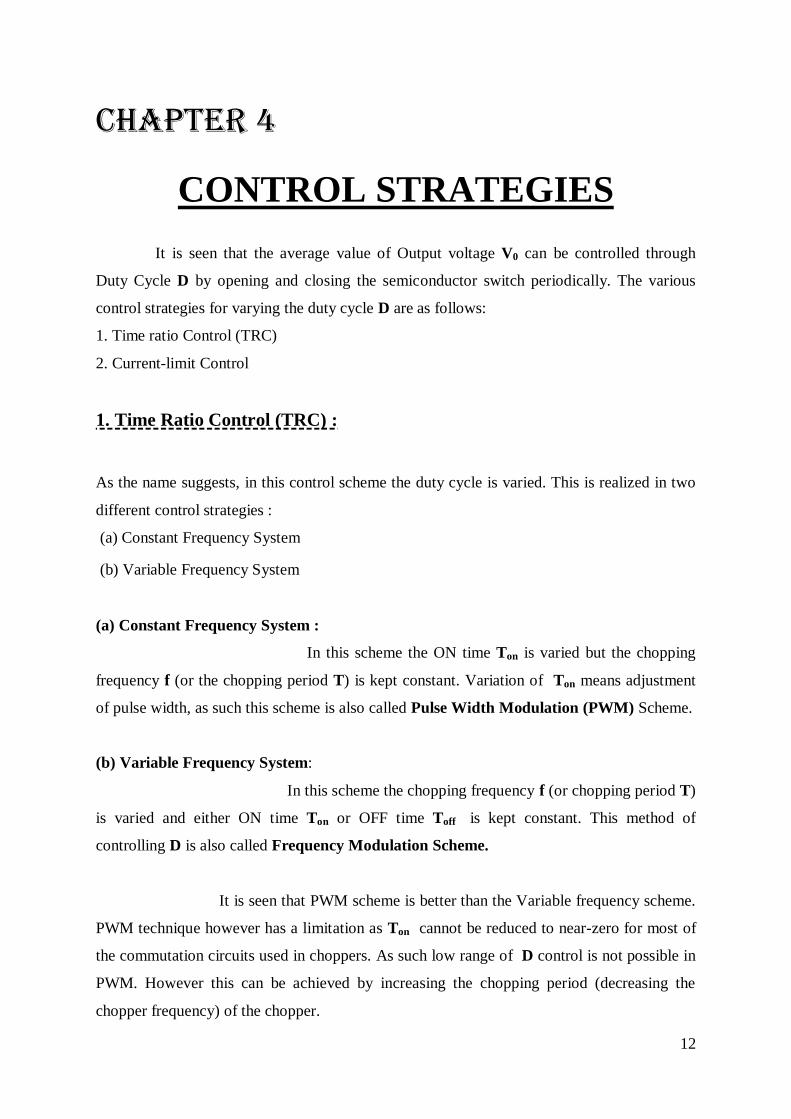
(a) Constant Frequency System :
In this scheme the ON time Ton is varied but the chopping
frequency f (or the chopping period T) is kept constant. Variation of Ton means adjustment
of pulse width, as such this scheme is also called Pulse Width Modulation (PWM) Scheme.
(b) Variable Frequency System:
In this scheme the chopping frequency f (or chopping period T)
is varied and either ON time Ton or OFF time Toff is kept constant. This method of
controlling D is also called Frequency Modulation Scheme.
It is seen that PWM scheme is better than the Variable frequency scheme.
PWM technique however has a limitation as Ton cannot be reduced to near-zero for most of
the commutation circuits used in choppers. As such low range of D control is not possible in
PWM. However this can be achieved by increasing the chopping period (decreasing the
chopper frequency) of the chopper.
13
Fig 4.1 : (a) on-time Ton constant (b) off-time Toff constant
14
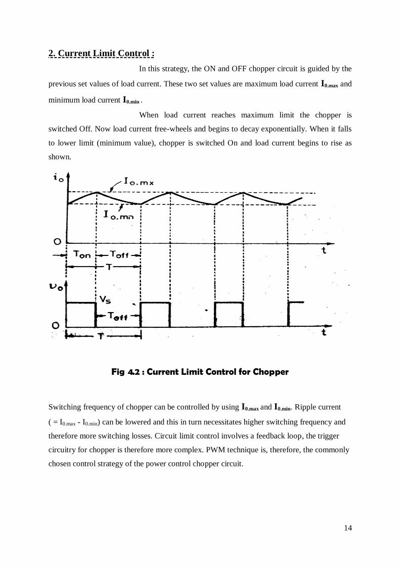
2. Current Limit Control :
In this strategy, the ON and OFF chopper circuit is guided by the
previous set values of load current. These two set values are maximum load current I0.max and
minimum load current I0.min .
When load current reaches maximum limit the chopper is
switched Off. Now load current free-wheels and begins to decay exponentially. When it falls
to lower limit (minimum value), chopper is switched On and load current begins to rise as
shown.
Fig 4.2 : Current Limit Control for Chopper
Switching frequency of chopper can be controlled by using I0.max and I0.min. Ripple current
( = I0.max - I0.min) can be lowered and this in turn necessitates higher switching frequency and
therefore more switching losses. Circuit limit control involves a feedback loop, the trigger
circuitry for chopper is therefore more complex. PWM technique is, therefore, the commonly
chosen control strategy of the power control chopper circuit.
15
Chapter 5
Switching Losses in MOSFET
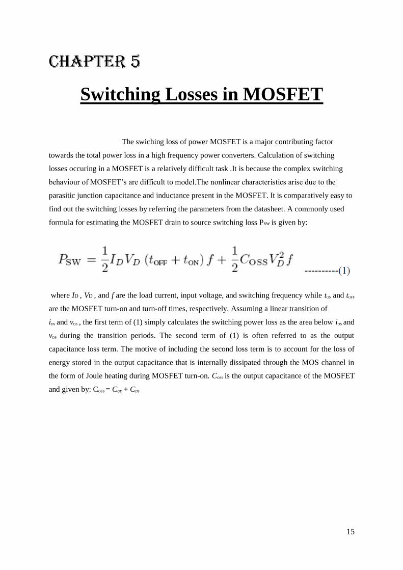
The swiching loss of power MOSFET is a major contributing factor
towards the total power loss in a high frequency power converters. Calculation of switching
losses occuring in a MOSFET is a relatively difficult task .It is because the complex switching
behaviour of MOSFET’s are difficult to model.The nonlinear characteristics arise due to the
parasitic junction capacitance and inductance present in the MOSFET. It is comparatively easy to
find out the switching losses by referring the parameters from the datasheet. A commonly used
formula for estimating the MOSFET drain to source switching loss Psw is given by:
where ID , VD , and f are the load current, input voltage, and switching frequency while tON and tOFF
are the MOSFET turn-on and turn-off times, respectively. Assuming a linear transition of
iDS and vDS , the first term of (1) simply calculates the switching power loss as the area below iDS and
vDS during the transition periods. The second term of (1) is often referred to as the output
capacitance loss term. The motive of including the second loss term is to account for the loss of
energy stored in the output capacitance that is internally dissipated through the MOS channel in
the form of Joule heating during MOSFET turn-on. COSS is the output capacitance of the MOSFET
and given by: COSS = CGD + CDS
16
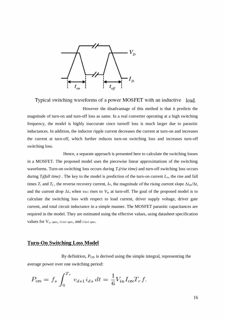
However the disadvantage of this method is that it predicts the
magnitude of turn-on and turn-off loss as same. In a real converter operating at a high switching
frequency, the model is highly inaccurate since turnoff loss is much larger due to parasitic
inductances. In addition, the inductor ripple current decreases the current at turn-on and increases
the current at turn-off, which further reduces turn-on switching loss and increases turn-off
switching loss.
Hence, a separate approach is presented here to calculate the switching losses
in a MOSFET. The proposed model uses the piecewise linear approximations of the switching
waveforms. Turn-on switching loss occurs during Tr(rise time) and turn-off switching loss occurs
during Tf(fall time) . The key to the model is prediction of the turn-on current ION, the rise and fall
times Tr and Tf , the reverse recovery current, Irr, the magnitude of the rising current slope Δids/Δt,
and the current drop Δi1f when vds1 rises to Vin at turn-off. The goal of the proposed model is to
calculate the switching loss with respect to load current, driver supply voltage, driver gate
current, and total circuit inductance in a simple manner. The MOSFET parasitic capacitances are
required in the model. They are estimated using the effective values, using datasheet specification
values for Vds1 spec, Crss1 spec, and Ciss1 spec.
Turn-On Switching Loss Model
By definition, PON is derived using the simple integral, representing the
average power over one switching period:
17
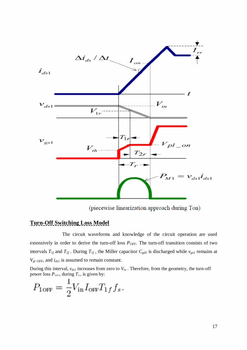
Turn-Off Switching Loss Model
The circuit waveforms and knowledge of the circuit operation are used
extensively in order to derive the turn-off loss POFF. The turn-off transition consists of two
intervals T1f and T2f . During T1f , the Miller capacitor Cgd1 is discharged while vgs1 remains at
Vpl OFF, and ids1 is assumed to remain constant.
During this interval, vds1 increases from zero to Vin . Therefore, from the geometry, the turn-off
power loss P1OFF, during T1f , is given by:
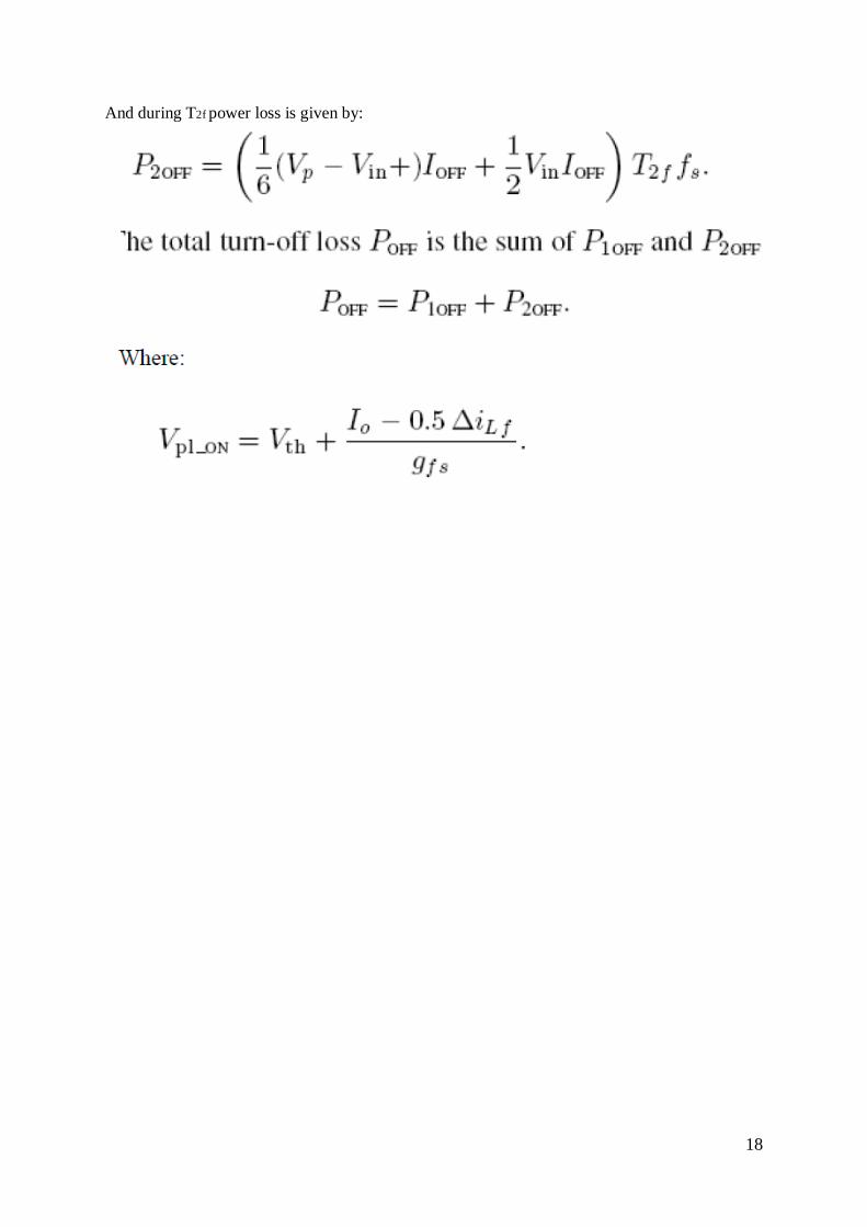
18
And during T2f power loss is given by:
19
Fig 5.2 : piecewise linearization approach during Toff
20
Chapter 6
ZERO VOLTAGE
SWITCHING RESONANT
CONVERTERS
21
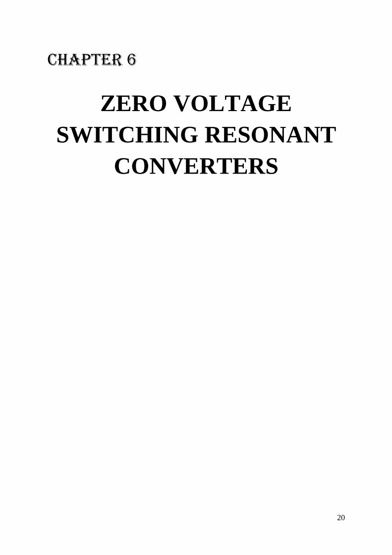
ZERO-VOLTAGE-SWITCHING RESONANT CONVERTERS
The switches of ZVS resonant converters turn on and off at zero voltage.
Fig 6.1 : Switch Configurations for ZVS Resonant Converters
The capacitor C is connected in parallel with the switch S1
to achieve ZVS. The internal switch capacitance Cj is added with the capacitor C and it
affects the resonant frequency only, thereby contributing no power dissipation in the switch.
If the switch is implemented with transistor Q1 and an anti-parallel diode D1 as shown, the
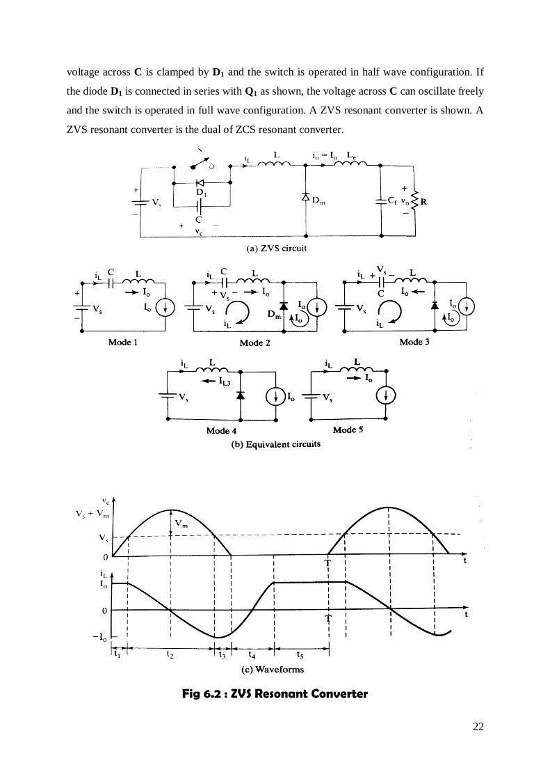
22
voltage across C is clamped by D1 and the switch is operated in half wave configuration. If
the diode D1 is connected in series with Q1 as shown, the voltage across C can oscillate freely
and the switch is operated in full wave configuration. A ZVS resonant converter is shown. A
ZVS resonant converter is the dual of ZCS resonant converter.
Fig 6.2 : ZVS Resonant Converter
23
The circuit operation can be divided into 5 modes whose circuits are
shown. We shall redefine the time origin t=0, at the beginning of each mode.
Mode 1 :
This mode is valid for 0 ≤ t ≤ t1. Both switch S1 and diode Dm are off. Capacitor C
charges at a constant rate of load current I0. The capacitor voltage Vc which rises is given by
Vc = Io.t / C
This mode ends at time t = t1 when Vc ( t = t1) = Vs. That is t1= Vs.C / I0.
Mode 2 :
This mode is valid for 0 ≤ t ≤ t2. The switch S1 is still off, but diode Dm turns
on. The capacitor voltate Vc is given by
Vc = Vmsin ω0t + Vs where Vm = I0√(L/C).
The peak switch voltage which occurs at t = (π/2) √LC, is
Vt(pk) = Vc(pk) = I0 √(L/C) + Vs
The inductor current iL is given by
iL = I0 cos ω0t
This mode ends at t = t2 when Vc (t = t2) = Vs, and iL(t = t2) = -I0. Therefore, t2 = π√LC.
Mode 3 :
This mode is valid for 0 ≤ t ≤ t3. The capacitor voltage that falls from Vs to zero is
given by
Vc = Vs - Vmsin ω0t
The inductor current iL is given by
iL = -I0 cos ω0t
This mode ends at t = t3 when Vc (t = t3) = 0, and iL (t = t3) = iL3. Thus,
T3 = √(LC) sin-1
x
Where, x = Vs/Vm = (Vs/I0) √(C/L).
24
Mode 4 :
This mode is valid for 0 ≤ t ≤ t4. Switch S1 is turned on and diode Dm remains
on. The inductor current which rises linearly from Il3 to I0 is given by
iL = IL3 + (Vs/L)t
This mode ends at time t = t4 when iL (t = t4) = 0. Thus t4 = (I0 – IL3)(L/Vs). IL3 has a negative
value.
Mode 5 :
This mode is valid for 0 ≤ t ≤ t5. Switch S1 is on but Dm is off. The load current I0
flows through the switch. This mode ends at time t = t5, when the switch S1 is turned off
again and the cycle is repeated. That is t5 = T – (t1 + t2 + t3 + t4).
The waveforms for iL and Vc are shown. The equation
Vt(pk) = Vc(pk) = I0 √(L/C) + Vs
shows that the peak switch voltage Vt(pk) is dependent on the load current I0. Therefore a
wide variation in the load current results in a wide variation of the switch voltage. For this
reason, ZVS converters are used only for constant-load applications. The switch must be
turned on only at zero voltage. Otherwise, the energy stored in C can be dissipated in the
switch. To avoid this situation, the antiparallel diode D1 must conduct before turning on the
switch.
25
Chapter 7
ZERO CURRENT
SWITCHING RESONANT
CONVERTERS
26
Why to go for ZCS
The control switches in all the PWM dc-dc converter
topologies, operate in a switch mode, in which they turn whole load current on and off during
each switching. This switch-mode operation subjects the control switches to high switching
stress and high switching power losses. To maximize the performance of switch-mode power
electronic conversion systems, the switching frequency of the power semiconductor devices
needs to be increased, but this results in increased switching losses and electromagnetic
interference (EMI). To eradicate these problems, Zero voltage switching (ZVS) technique
and zero current switching (ZCS) technique are two conventionally employed soft switching
methods. These techniques lead to either zero voltage or zero current during switching
transition, significantly decreasing the switching losses and increasing the reliability for the
converters. The ZVS technique eliminates capacitive turn-on losses, and decreases the turn-
off switching losses by slowing down the voltage rise, thereby lowering the overlap between
the switch voltage and the switch current. However, a large external resonant capacitor is
needed to lower the turn-off switching loss effectively for ZVS. Conversely, ZCS eliminates
the voltage and current overlap by forcing the switch current to zero before the switch voltage
rises, making it more effective than ZVS in reducing switching losses, especially for slow
switching power devices. For high efficiency power conversion, the ZCS topologies are most
frequently adopted.
Variable frequency control can achieve output regulation of the
resonant converters in both traditional ZCS and ZVS approaches. Traditional ZCS converters
operate with constant on-time control, while the traditional ZVS converters operate with
constant off-time control. Both approaches need to operate with a wide switching frequency
range when given a wide input source and load range, making the filter circuit design difficult
to optimize. Many high efficiency converter topologies with ZCS have been explored and
proposed. The primary design feature of novel ZCS/ZVS PWM power converters is the
incorporation of an auxiliary switch in the traditional quasi-resonant circuit. The resonance of
the novel converters is dominated by the auxiliary switch, which generates resonance and
temporarily stops a period that can be regulated, thus circumventing the disadvantages of
fixed conduction or cut-off time in a traditional quasi-resonant power converter.
27
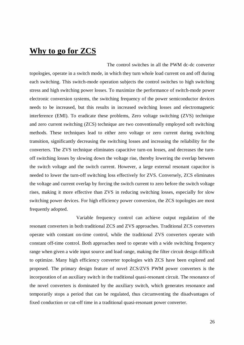
ZERO CURRENT SWITCHING RESONANT CONVERTERS
The switches of Zero Current Switching (ZCS) resonant converters turn ON
and OFF at zero current. The resonant circuit that consists of switch S1, inductor L, and
capacitor C is shown. The inductor L is connected in series with power switch S1 to achieve
ZCS. It is classified into two types – L type and M type. In both the types the inductor L
limits the di/dt of the switch current and L and C constitute a series resonant circuit. When
the switch current is zero there is a current i=Cj.dvt/dt flowing through the internal
capacitance Cj due to finite slope of switch voltage at turn off. This current flow causes
power dissipation in the switch and limits the high switching frequency.
Fig 7.1 : Switch configurations for ZCS Resonant Converters
28
The switch can be implemented either in half wave
configuration where diode D1 allows unidirectional current flow or in full-wave
configuration where the switch current can flow bidirectionally. The practical devices do not
turn off at zero current due to their recovery time. As a result, an amount of energy can be
trapped in inductor L of the M-type configuration and voltage transients appear across the
switch. This normally favours L-type configuration over M-type one.
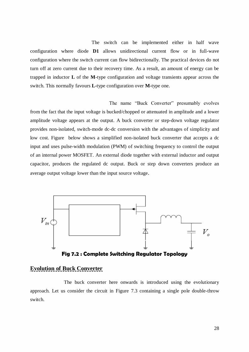
The name “Buck Converter” presumably evolves
from the fact that the input voltage is bucked/chopped or attenuated in amplitude and a lower
amplitude voltage appears at the output. A buck converter or step-down voltage regulator
provides non-isolated, switch-mode dc-dc conversion with the advantages of simplicity and
low cost. Figure below shows a simplified non-isolated buck converter that accepts a dc
input and uses pulse-width modulation (PWM) of switching frequency to control the output
of an internal power MOSFET. An external diode together with external inductor and output
capacitor, produces the regulated dc output. Buck or step down converters produce an
average output voltage lower than the input source voltage.
Fig 7.2 : Complete Switching Regulator Topology
Evolution of Buck Converter
The buck converter here onwards is introduced using the evolutionary
approach. Let us consider the circuit in Figure 7.3 containing a single pole double-throw
switch.
29
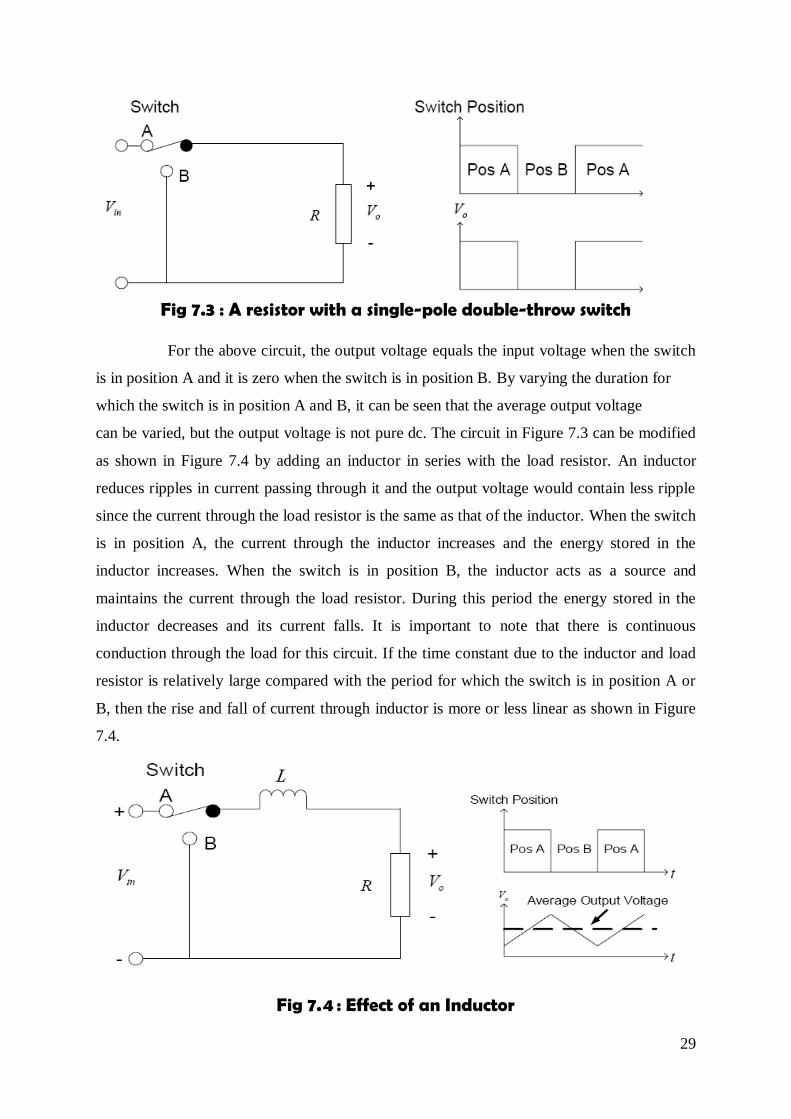
Fig 7.3 : A resistor with a single-pole double-throw switch
For the above circuit, the output voltage equals the input voltage when the switch
is in position A and it is zero when the switch is in position B. By varying the duration for
which the switch is in position A and B, it can be seen that the average output voltage
can be varied, but the output voltage is not pure dc. The circuit in Figure 7.3 can be modified
as shown in Figure 7.4 by adding an inductor in series with the load resistor. An inductor
reduces ripples in current passing through it and the output voltage would contain less ripple
since the current through the load resistor is the same as that of the inductor. When the switch
is in position A, the current through the inductor increases and the energy stored in the
inductor increases. When the switch is in position B, the inductor acts as a source and
maintains the current through the load resistor. During this period the energy stored in the
inductor decreases and its current falls. It is important to note that there is continuous
conduction through the load for this circuit. If the time constant due to the inductor and load
resistor is relatively large compared with the period for which the switch is in position A or
B, then the rise and fall of current through inductor is more or less linear as shown in Figure
7.4.
Fig 7.4 : Effect of an Inductor
30
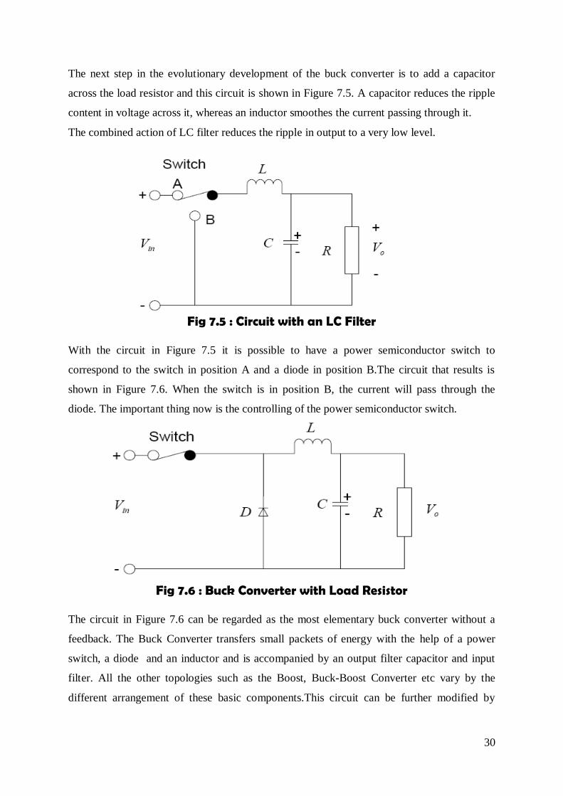
The next step in the evolutionary development of the buck converter is to add a capacitor
across the load resistor and this circuit is shown in Figure 7.5. A capacitor reduces the ripple
content in voltage across it, whereas an inductor smoothes the current passing through it.
The combined action of LC filter reduces the ripple in output to a very low level.
Fig 7.5 : Circuit with an LC Filter
With the circuit in Figure 7.5 it is possible to have a power semiconductor switch to
correspond to the switch in position A and a diode in position B.The circuit that results is
shown in Figure 7.6. When the switch is in position B, the current will pass through the
diode. The important thing now is the controlling of the power semiconductor switch.
Fig 7.6 : Buck Converter with Load Resistor
The circuit in Figure 7.6 can be regarded as the most elementary buck converter without a
feedback. The Buck Converter transfers small packets of energy with the help of a power
switch, a diode and an inductor and is accompanied by an output filter capacitor and input
filter. All the other topologies such as the Boost, Buck-Boost Converter etc vary by the
different arrangement of these basic components.This circuit can be further modified by
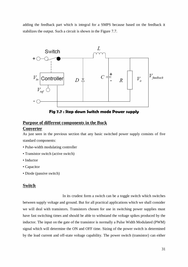
31
adding the feedback part which is integral for a SMPS because based on the feedback it
stabilizes the output. Such a circuit is shown in the Figure 7.7.
Fig 7.7 : Step down Switch mode Power supply
Purpose of different components in the Buck
Converter
As just seen in the previous section that any basic switched power supply consists of five
standard components:
• Pulse-width modulating controller
• Transistor switch (active switch)
• Inductor
• Capacitor
• Diode (passive switch)
Switch
In its crudest form a switch can be a toggle switch which switches
between supply voltage and ground. But for all practical applications which we shall consider
we will deal with transistors. Transistors chosen for use in switching power supplies must
have fast switching times and should be able to withstand the voltage spikes produced by the
inductor. The input on the gate of the transistor is normally a Pulse Width Modulated (PWM)
signal which will determine the ON and OFF time. Sizing of the power switch is determined
by the load current and off-state voltage capability. The power switch (transistor) can either
32
be a MOSFET, IGBT, JFET or a BJT. Power MOSFETs are the key elements of high
frequency power systems such as high-density power supplies. Therefore MOSFETs have
now replaced BTJ’s in new designs operating at much higher frequencies but at lower
voltages. At high voltages MOSFETs still have their limitations. The intrinsic characteristics
of the MOSFET produce a large on-resistance which increases excessively when the devices
breakdown voltage is raised. Therefore the power MOSFET is only useful upto voltage
ratings of 500V and so is restricted to low voltage applications or in two-transistor forward
converters and bridge circuits operating off-line. At high breakdown voltages (>200V) the
on-state voltage drop of the power MOSFET becomes higher than that of a similar size
bipolar device with similar voltage rating. This makes it more attractive to use the bipolar
power transistor at the expense of worse high frequency performance. As improvements in
fabrication techniques, new materials, device characteristics take place than MOSFETs are
likely to replace BJTs.
Operating Frequency
The operating frequency determines the performance of the switch.
Switching frequency selection is typically determined by efficiency requirements. There is
now a growing trend in research work and new power supply designs in increasing the
switching frequencies.The higher is the switching frequency, the smaller the physical size and
component value. The reason for this is to reduce even further the overall size of the power
supply in line with miniaturisation trends in electronic and computer systems. However there
is an upper frequency limit where either magnetic losses in the inductor or switching losses in
the regulator circuit and power MOSFET reduce efficiency to an impractical level. Higher
frequency also reduces the size of the output capacitor. E.g. the capacitance required is
67μF at 500 KHz, but only 33μF at 1MHz.The ripple current specification remains
unchanged.
Inductor
The function of the inductor is to limit the current slew rate (limit the
current in rush) through the power switch when the circuit is ON. The current through the
inductor cannot change suddenly. When the current through an inductor tends to fall, the
inductor tends to maintain the current by acting as a source. This limits the otherwise high-
peak current that would be limited by the switch resistance alone. The key advantage is when
the inductor is used to drop voltage, it stores energy. Also the inductor controls the percent of
33
the ripple and determines whether or not the circuit is operating in the continuous mode. Peak
current through the inductor determines the inductor’s required saturation current rating,
which in turn dictates the approximate size of the inductor. Saturating the inductor core
decreases the converter efficiency, while increasing the temperature of the inductor, the
MOSFET and the diode. The size of the inductor and capacitor can be reduced by the
implementation of high switching frequency, multiphase interleaved topology, and a fast
hysteric controller. A smaller inductor value enables a faster transient response, it also results
in larger current ripple which causes higher conduction losses in the switches, inductor and
parasitic resistances. The smaller inductor also requires a larger filter capacitor to decrease
the output voltage ripple. Inductors used in switched supplies are sometimes wound on
toroidal cores, often made of ferrite or powdered iron core with distributed air-gap to store
energy.
A DC-DC converter transfers energy at a controlled rate from an input
source to an output load, and as the switching frequency increases, the time available for this
energy transfer decreases. For example, consider a buck converter operating at 500 kHz with
a 10 μH inductor. For most DC-DC converters, changing the frequency to 1 MHz allows use
of exactly one half the inductance, or 5μH.
Capacitor
Capacitor provides the filtering action by providing a path for the
harmonic currents away from the load. Output capacitance (across the load) is required to
minimize the voltage overshoot and ripple present at the output of a step-down converter. The
capacitor is large enough so that its voltage does not have any noticeable change during the
time the switch is off. Large overshoots are caused by insufficient output capacitance, and
large voltage ripple is caused by insufficient capacitance as well as a high equivalent-series
resistance (ESR) in the output capacitor. The maximum allowed output-voltage overshoot
and ripple are usually specified at the time of design. Thus, to meet the ripple specification
for a step-down converter circuit, we must include an output capacitor with ample
capacitance and low ESR.
The problem of overshoot, in which the output-voltage overshoots
its regulated value when a full load is suddenly removed from the output, requires that the
output capacitor be large enough to prevent stored inductor energy from launching the output
above the specified maximum output voltage. Since switched power regulators are usually
used in high current, high performance power supplies, the capacitor should be chosen for
34
minimum loss. Loss in a capacitor occurs because of its internal series resistance and
inductance. Capacitors for switched regulators are partly chosen on the basis of Effective
Series Resistance (ESR). Solid tantalum capacitors are the best in this respect. For very high
performance power supplies, sometimes it is necessary to use parallel capacitors to get a low
enough effective series resistance.
Freewheeling Diode
Since the current in the inductor cannot change suddenly, a path must
exist for the inductor current when the switch is off (open). This path is provided by the
freewheeling diode (or catch diode).The purpose of this diode is not to rectify, but to direct
current flow in the circuit and to ensure that there is always a path for the current to flow into
the inductor. It is also necessary that this diode should be able to turn off relatively fast. Thus
the diode enables the converter to convert stored energy in the inductor to the load. This is a
reason why we have higher efficiency in a DC-DC Converter as compared to a linear
regulator. When the switch closes, the current rises linearly (exponentially if resistance is also
present). When the switch opens, the freewheeling diode causes a linear decrease in current.
At steady state we have a saw tooth response with an average value of the current.
Feedback
Feedback and control circuitry can be carefully nested around these
circuits to regulate the energy transfer and maintain a constant output within normal
operating conditions. Control by pulse-width modulation is necessary for regulating the
output. The transistor switch is the heart of the switched supply and it controls the power
supplied to the load.
L-TYPE ZCS RESONANT CONVERTER
The circuit operation can be divided into 5 modes whose equivalent
circuits are shown. We shall redefine the time origin, t=0, at the beginning of each mode.
Mode 1 :
This mode is valid for 0 < t < t1. Switch S1 is turned on and diode Dm conducts.
The inductor current iL which rises linearly is given by
IL = (Vs/L)t
This mode ends at time t=t1 when il (t=t1) = I0. That is t1 = I0L/Vs,
35
Mode 2 :
This mode is valid for 0 < t < t2. Switch S1 remains on but diode Dm is off.
The inductor current iL is given by
iL=Imsin ωot + I0
where Im = Vs√(C/L) and ω0 = 1/√LC. The capacitor voltage Vc is given by
Vc = Vs(1 – cosω0t)
The peak current which occurs at t = (π/2)√LC is
Ip = Im + I0
The peak capacitor voltage is given by
Vc(pk) = 2Vs
This mode ends at t = t2 when iL(t = t2) = I0 and Vc( t = t2 ) = Vc2 = 2Vs. Therefore t2 = π√LC.
Mode 3 :
This mode is valid for 0 < t < t3. The inductor current that falls from I0 to zero
is given by
iL = I0 – Imsinω0t
36
The capacitor voltage is given by
Vc = 2Vscosω0t
This mode ends at t = t3 when iL (t = t3 ) = 0. And Vc(t = t3) = Vc3. Thus t3 = √LCsin-1
(1/x)
where x = Im/I0 = (Vs/I0)√C/L
Mode 4 :
This mode is valid for 0 < t < t4. The capacitor supplies the load current Io and
its voltage is given by
Vc = Vc3 – (I0/C)t
This mode ends at t = t4 when Vc (t = t4) = 0. Thus t4 = Vc3C/I0
Fig 7.7 : L-Type ZCS Resonant Converter
Mode 5 :
This mode is valid for 0 < t < t5. When the capacitor voltage tends to be
negative, the diode Dm conducts. The load current Io flows through diode Dm. This mode ends
at time t=t5 when the switch S1 is turned on again and the cycle is repeated i.e. t5=T-
(t1+t2+t3+t4).
The waveform for Il and Vc are shown. The peak switch voltage equals
the dc supply voltage because the switch current is zero at turn on and turn off, the switching
loss, which is the product of V and I, becomes very small. The peak resonant current Im must
be higher than the load current Io and this sets a limit on the minimum value of load

37
resistance R. However by placing an anti-parallel diode across the switch, the output voltage
can be made insensitive to load variations.
38
Chapter 8
IMPLEMENTATION
WORK &
OBSERVATIONS
39
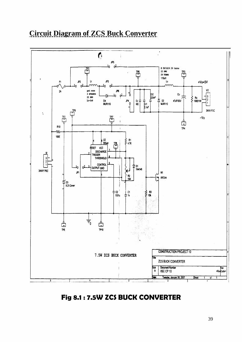
Circuit Diagram of ZCS Buck Converter
Fig 8.1 : 7.5W ZCS BUCK CONVERTER
40
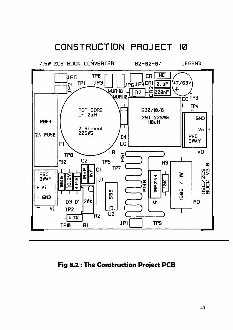
Fig 8.2 : The Construction Project PCB
41
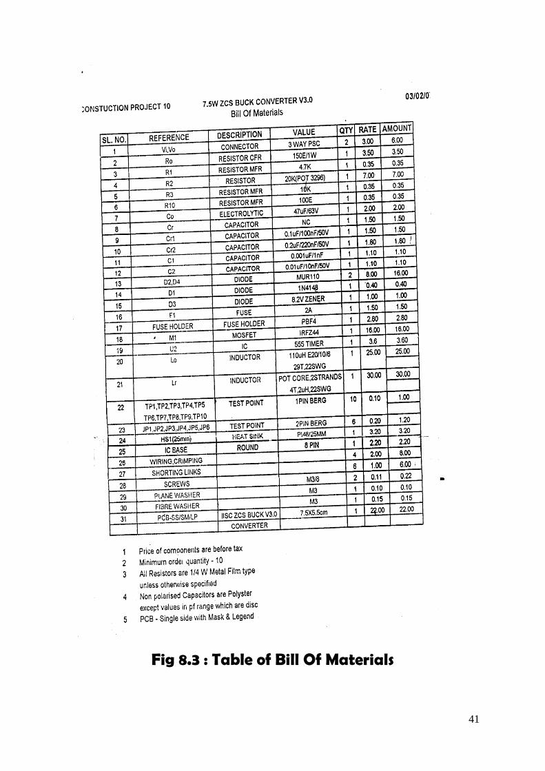
Fig 8.3 : Table of Bill Of Materials
42
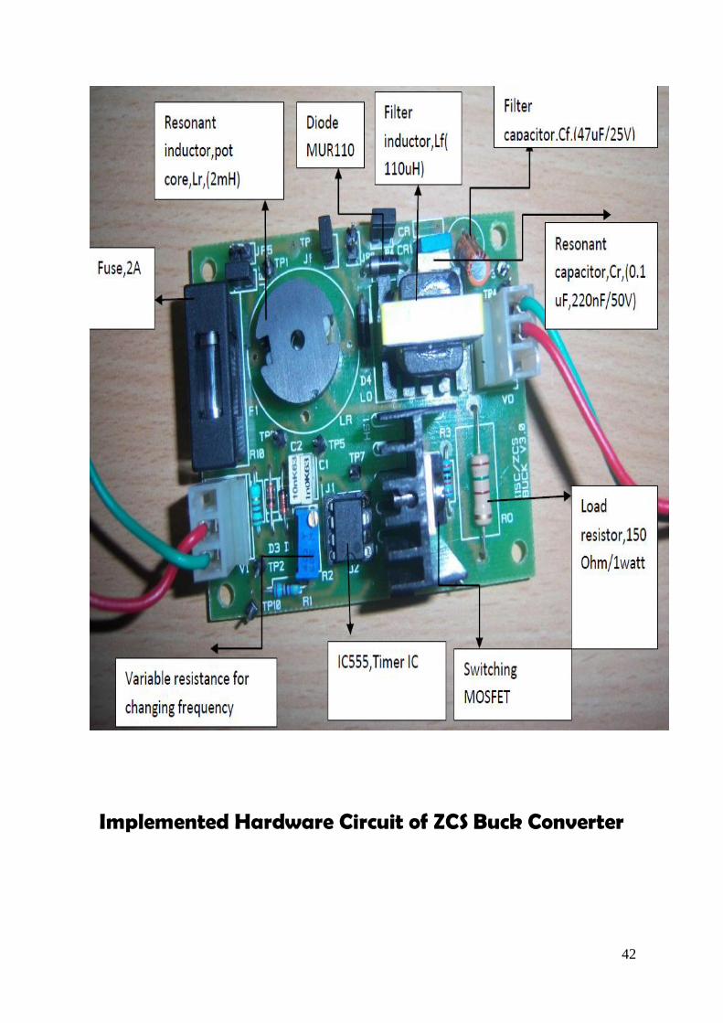
Implemented Hardware Circuit of ZCS Buck Converter
43
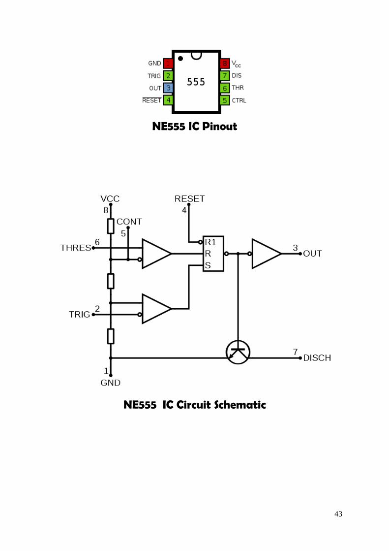
NE555 IC Pinout
NE555 IC Circuit Schematic
44
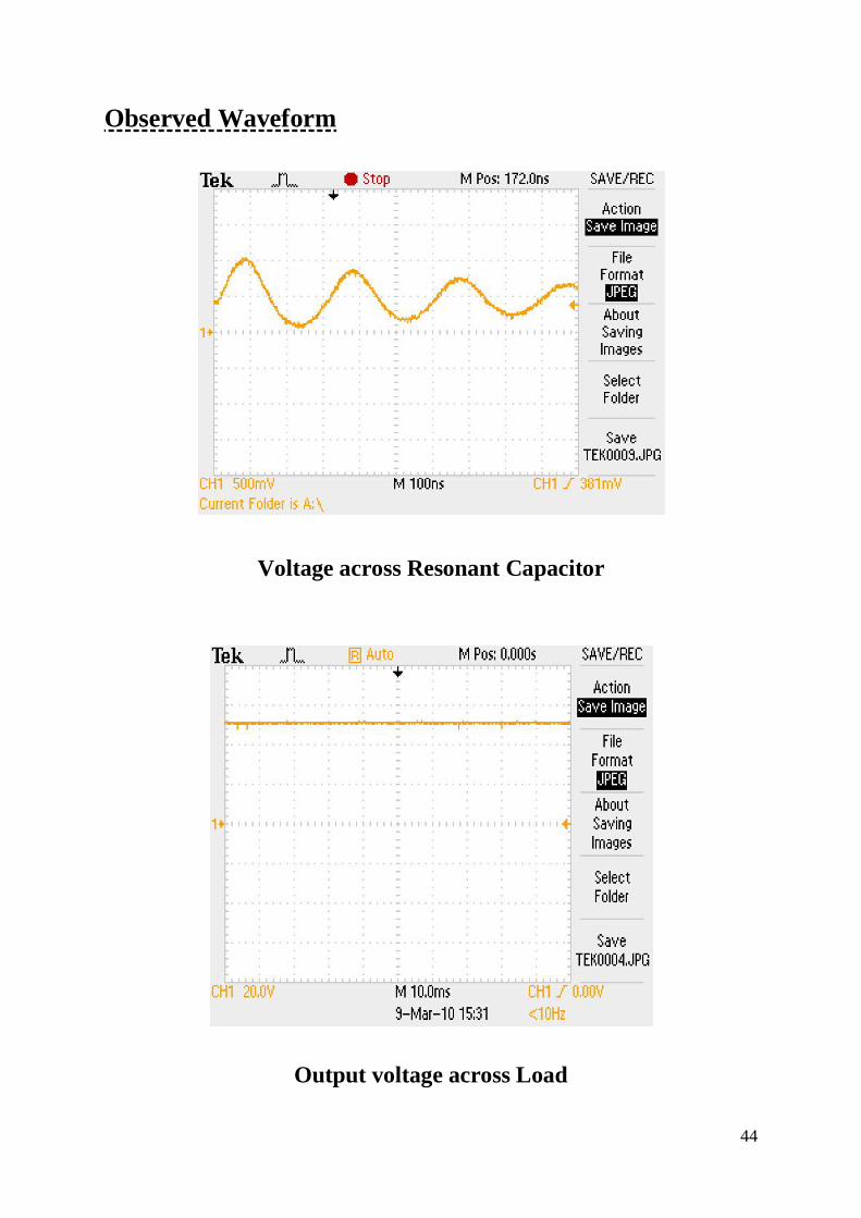
Observed Waveform
Voltage across Resonant Capacitor
Output voltage across Load
45
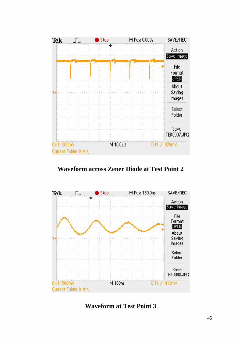
Waveform across Zener Diode at Test Point 2
Waveform at Test Point 3
46
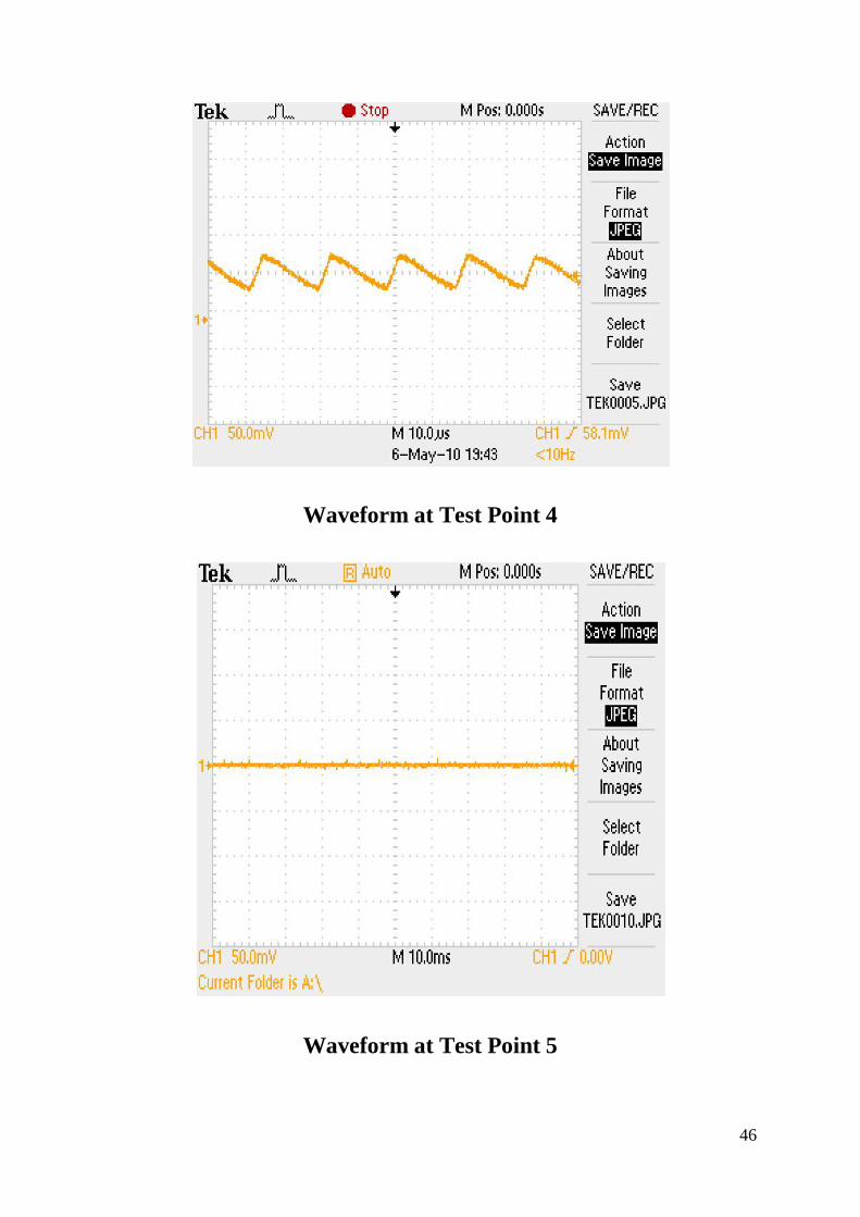
Waveform at Test Point 4
Waveform at Test Point 5
47
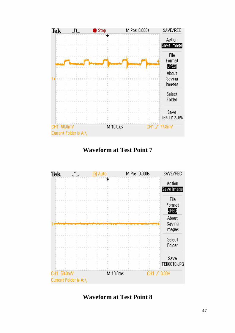
Waveform at Test Point 7
Waveform at Test Point 8
48
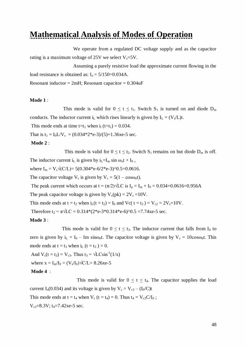
Mathematical Analysis of Modes of Operation
We operate from a regulated DC voltage supply and as the capacitor
rating is a maximum voltage of 25V we select Vs=5V.
Assuming a purely resistive load the approximate current flowing in the
load resistance is obtained as: Io = 5/150=0.034A.
Resonant inductor = 2mH; Resonant capacitor = 0.304uF
Mode 1 :
This mode is valid for 0 < t < t1. Switch S1 is turned on and diode Dm
conducts. The inductor current iL which rises linearly is given by IL = (Vs/L)t.
This mode ends at time t=t1 when il (t=t1) = 0.034.
That is t1 = I0L/Vs = (0.034*2*e-3)/(5)=1.36xe-5 sec.
Mode 2 :
This mode is valid for 0 < t < t2. Switch S1 remains on but diode Dm is off.
The inductor current iL is given by iL=Im sin ωot + I0 ,
where Im = Vs√(C/L)= 5(0.304*e-6/2*e-3)^0.5=0.0616.
The capacitor voltage Vc is given by Vc = 5(1 – cosω0t).
The peak current which occurs at t = (π/2)√LC is Ip = Im + I0 = 0.034+0.0616=0.956A
The peak capacitor voltage is given by Vc(pk) = 2Vs =10V.
This mode ends at t = t2 when iL(t = t2) = I0 and Vc( t = t2 ) = Vc2 = 2Vs=10V.
Therefore t2 = π√LC = 0.314*(2*e-3*0.314*e-6)^0.5 =7.74xe-5 sec.
Mode 3 :
This mode is valid for 0 < t < t3. The inductor current that falls from I0 to
zero is given by iL = I0 – Im sinω0t. The capacitor voltage is given by Vc = 10cosω0t. This
mode ends at t = t3 when iL (t = t3 ) = 0.
And Vc(t = t3) = Vc3. Thus t3 = √LCsin-1
(1/x)
where x = Im/I0 = (Vs/I0)√C/L= 8.26xe-5
Mode 4 :
This mode is valid for 0 < t < t4. The capacitor supplies the load
current Io(0.034) and its voltage is given by Vc = Vc3 – (I0/C)t
This mode ends at t = t4 when Vc (t = t4) = 0. Thus t4 = Vc3C/I0 ;
Vc3=8.3V; t4=7.42xe-5 sec.

49
Mode 5 :
This mode is valid for 0 < t < t5. When the capacitor voltage
tends to be negative, the diode Dm conducts. The load current Io flows through diode Dm.
This mode ends at time t=t5 when the switch S1 is turned on again and the cycle is repeated
i.e. t5=T-(t1+t2+t3+t4).
For the sake of simplicity we assume t5=0.
Therefore Ton = t1+t2+t3= 17.36xe-5
Toff = t4+t5= t4 = 7.42xe-5
T= Ton + Toff = 24.78xe-5
Duty ratio = Ton/T = 70.05%
Frequency of operation = 1/T = 4KHz.
50
Conclusion
ZCS buck converter is an efficient step down DC-DC
converter used in numerous electronics devices. The same was implemented as a hardware
project and an output voltage of 2V was obtained with an input of 5.32V DC supply. The
time analysis of various modes of zcs buck converter was done and tuning of the IC555 was
done accordingly. Also the waveforms across capacitors and various test points were
obtained, studied and compared with the theoretical waveforms. The waveforms were found
to be in precise proximity of theoretical waveforms.
51
Reference
Rashid H.Muhammad, Power Electronics – Circuits, Devices and Applications,
Prentice Hall India, 2004
Bimbra P. S., Power Electronics, Khanna Publishers, 2007
Muhammad Saad Rahman, Master thesis in Electronic Devices at Linköping Institute
of Technology, Buck Converter Design Issues.
Yali Xiong, Shan Sun, Hongwei Jia, Patrick Shea and Z. John Shen, IEEE
TRANSACTIONS ON POWER ELECTRONICS, VOL. 24, NO. 2, FEBRUARY
2009, New Physical Insights on Power MOSFET Switching Losses.
Wilson Eberle, Zhiliang Zhang, Yan-Fei Liu and Paresh C. Sen ; IEEE
TRANSACTIONS ON POWER ELECTRONICS, VOL. 24, NO. 3, MARCH 2009,
A Practical Switching Loss Model for Buck Voltage Regulators.
NE555 Datasheet and Circuit Schematic Overview
http://datasheetreference.com/ne555-datasheet.html
Top Related