Z80182/Z8L182 PS Mstr
109
3-1 DS971820600 FEATURES P RELIMINARY P RODUCT S PECIFICATION ■ Z8S180 MPU - Code Compatible with Zilog Z80 ® /Z180 ™ CPU - Extended Instructions - Operating Frequency: 33 MHz/5V or 20 MHz/3.3V - Two DMA Channels - On-Chip Wait State Generators - Two UART Channels - Two 16-Bit Timer Counters - On-Chip Interrupt Controller - On-Chip Clock Oscillator/Generator - Clocked Serial I/O Port - Fully Static - Low EMI Option ■ Two ESCC ™ Channels with 32-Bit CRC ■ Three 8-Bit Parallel I/O Ports ■ 16550 Compatible MIMIC Interface for Direct Connection to PC, XT, AT Bus ■ 100-Pin Package Styles (QFP, VQFP) (0.8 Micron CMOS 5120 Technology) ■ Individual WSG for RAMCS and ROMCS GENERAL DESCRIPTION The Z80182/Z8L182 is a smart peripheral controller IC for modem (in particular V. Fast applications), fax, voice messaging and other communications applications. It uses the Z80180 microprocessor (Z8S180 MPU core) linked with two channels of the industry standard Z85230 ESCC (Enhanced Serial Communications Controller), 24 bits of parallel I/O, and a 16550 MIMIC for direct connection to the IBM PC, XT, AT bus. The Z80182/Z8L182 allows complete flexibility for both internal PC and external applications. Also current PC modem software compatibility can be maintained with the Z80182/Z8L182 ability to mimic the 16550 UART chip. The Z80180 acts as an interface between the ESCC ™ and 16550 MIMIC interface when used in internal applications, and between the two ESCC channels in the external applications. This interface allows data compression and error correction on outgoing and incoming data. In external applications, three 8-bit parallel ports are available for driving LEDs or other devices. Figure 1 shows the Z80182/ Z8L182 block diagram, while the pin assignments for the QFP and the VQFP packages are shown in Figures 2 and 3, respectively. All references in this document to the Z80182, or Z182 refer to both the Z80182 and Z8L182. Notes: All Signals with a preceding front slash, "/", are active Low, e.g., B//W (WORD is active Low); /B/W (BYTE is active Low, only). Power connections follow conventional descriptions below: Connection Circuit Device Power V CC V DD Ground GND V SS Z80182/Z8L182 ZILOG INTELLIGENT PERIPHERAL CONTROLLER (ZIP ™ )
Transcript of Z80182/Z8L182 PS Mstr
3-1
Z80182/Z8L182ZILOG INTELLIGENT PERIPHERALP R E L I M I N A R YZilog
DS971820600
FEATURES
PRELIMINARY PRODUCT SPECIFICATION
Z8S180 MPU- Code Compatible with Zilog Z80®/Z180™ CPU- Extended Instructions- Operating Frequency: 33 MHz/5V or 20 MHz/3.3V- Two DMA Channels- On-Chip Wait State Generators- Two UART Channels- Two 16-Bit Timer Counters- On-Chip Interrupt Controller- On-Chip Clock Oscillator/Generator- Clocked Serial I/O Port- Fully Static- Low EMI Option
Two ESCC™ Channels with 32-Bit CRC
Three 8-Bit Parallel I/O Ports
16550 Compatible MIMIC Interface forDirect Connection to PC, XT, AT Bus
100-Pin Package Styles (QFP, VQFP)(0.8 Micron CMOS 5120 Technology)
Individual WSG for RAMCS and ROMCS
GENERAL DESCRIPTION
The Z80182/Z8L182 is a smart peripheral controller IC formodem (in particular V. Fast applications), fax, voicemessaging and other communications applications. Ituses the Z80180 microprocessor (Z8S180 MPU core)linked with two channels of the industry standard Z85230ESCC (Enhanced Serial Communications Controller), 24bits of parallel I/O, and a 16550 MIMIC for direct connectionto the IBM PC, XT, AT bus.
The Z80182/Z8L182 allows complete flexibility for bothinternal PC and external applications. Also current PCmodem software compatibility can be maintained with theZ80182/Z8L182 ability to mimic the 16550 UART chip. TheZ80180 acts as an interface between the ESCC™ and16550 MIMIC interface when used in internal applications,and between the two ESCC channels in the externalapplications. This interface allows data compression and
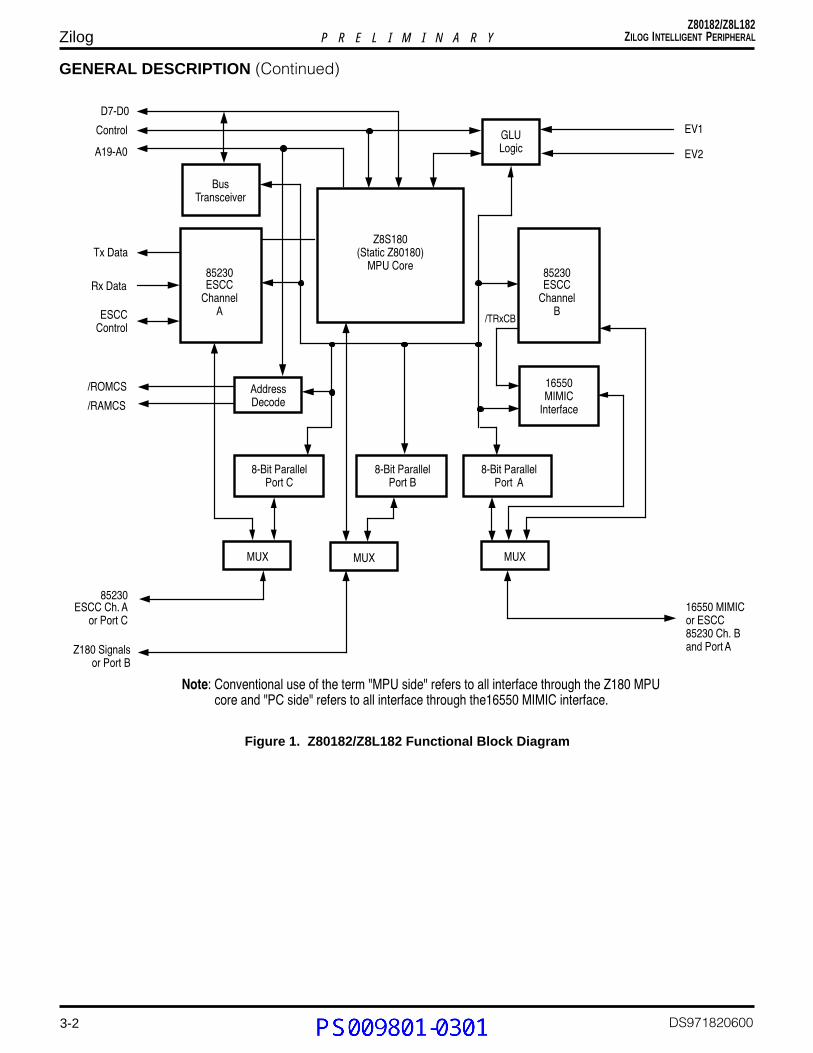
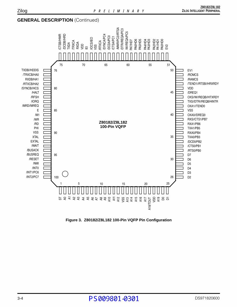
error correction on outgoing and incoming data. In externalapplications, three 8-bit parallel ports are available fordriving LEDs or other devices. Figure 1 shows the Z80182/Z8L182 block diagram, while the pin assignments for theQFP and the VQFP packages are shown in Figures 2 and3, respectively. All references in this document to theZ80182, or Z182 refer to both the Z80182 and Z8L182.
Notes:All Signals with a preceding front slash, "/", are active Low, e.g.,B//W (WORD is active Low); /B/W (BYTE is active Low, only).
Power connections follow conventional descriptions below:
Connection Circuit Device
Power VCC VDD
Ground GND VSS
Z80182/Z8L182ZILOG INTELLIGENT PERIPHERALCONTROLLER (ZIP™)
Gayle Gamble
PS009801-0301
3-2
Z80182/Z8L182ZILOG INTELLIGENT PERIPHERALP R E L I M I N A R YZilog
DS971820600
GENERAL DESCRIPTION (Continued)
Z8S180(Static Z80180)
MPU Core
AddressDecode
8-Bit ParallelPort C
8-Bit ParallelPort B
8-Bit ParallelPort A
85230ESCC
Channel B
MUX MUX
16550MIMIC
Interface
EV1
EV2
D7-D0
Control
A19-A0
Tx Data
Rx Data
ESCCControl
/ROMCS
/RAMCS
GLULogic
85230ESCC
Channel A
BusTransceiver
MUX
/TRxCB
16550 MIMICor ESCC 85230 Ch. Band Port A
85230ESCC Ch. A
or Port C
Z180 Signalsor Port B
Note: Conventional use of the term "MPU side" refers to all interface through the Z180 MPU core and "PC side" refers to all interface through the16550 MIMIC interface.
Figure 1. Z80182/Z8L182 Functional Block Diagram
Gayle Gamble
PS009801-0301
Gayle Gamble

3-3
Z80182/Z8L182ZILOG INTELLIGENT PERIPHERALP R E L I M I N A R YZilog
DS971820600
/TRXCB/HA0
TXDB//HDDIS
/CTSB//HWR
/DCDB//HRD
TXDA
/TRXCA
RXDA
/NM
I/R
ESET
/BU
SREQ
/BU
SAC
K
EXTA
L
XTAL
VSS
PHI
/RD
/WR
/M1
E /MR
D//M
REQ
/IOR
Q
/RFS
H
/HAL
T
/SYN
CB/
/HC
S
/RTX
CB/
HA2
RXD
B/H
A1
/WAI
T
Z80182/Z8L182100-Pin QFP
/INT0
/INT1/PC6
/INT2/PC7
ST
A0
A1
A2
A3A4
A5
A6
A7
A8
A9
A10
A11
A12
VSS
A13
A14
A15
A16
A17
A18/TOUTVDD
A19
D0
D1
D2
D3
VDD
IEI
/IOCS/IEO
VSS
/RTXCA
/SYNCA/PC4
/DCDA/PC0
/CTSA/PC1
/MWR/PC2//RTSA
/DTR//REQA/PC3
/W//REQA/PC5
PA7/HD7
PA6/HD6
PA5/HD5
PA4/HD4
PA3/HD3
PA2/HD2
PA1/HD1
PA0/HD0
EV2
EV1
/ROMCS
/RAMCS
1001 95
5
10
15
90 8580
75
70
65
60
55
5045403530
25
20
D4
D5
D6
D7
/RTS
0/PB
0/C
TS0/
PB1
/DC
D0/
PB2
TXA0
/PB3
RXA
1/PB
6
RX
S//C
TS
1/P
B7
TX
S//D
TR
//RE
QB
//HIN
TR
CKS
//W//R
EQB/
/HTX
RD
Y/D
REQ
1
VDD
/TEN
D1/
/RTS
B//H
RXR
DY
CKA
1//T
END
0
RXA
0/PB
4
TXA1
/PB5
CKA
0//D
REQ
0
VSS
Figure 2. Z80182/Z8L182 100-Pin QFP Pin Configuration
Gayle Gamble
PS009801-0301
3-4
Z80182/Z8L182ZILOG INTELLIGENT PERIPHERALP R E L I M I N A R YZilog
DS971820600
GENERAL DESCRIPTION (Continued)
Z80182/Z8L182100-Pin VQFP
EV1/ROMCS/RAMCS/TEND1//RTSB//HRXRDYVDD/DREQ1CKS//W//REQB//HTXRDYTXS//DTR//REQB/HINTRCKA1//TEND0VSSCKA0//DREQ0RXS//CTS1/PB7RXA1/PB6TXA1/PB5RXA0/PB4TXA0/PB3/DCD0/PB2/CTS0/PB1/RTS0/PB0D7D6D5D4D3D2
1 25
/CTS
B//H
WR
/DC
DB/
/HR
DTX
DA
/TR
XCA
RXD
AVD
DIE
I
/IOC
S/IE
OVS
S/R
TXC
A/S
YNC
A/PC
4/D
CD
A/PC
0/C
TSA/
PC1
/MW
R/P
C2/
/RTS
A/D
TR//R
EQA/
PC3
/W//R
EQA/
PC5
PA7/
HD
7PA
6/H
D6
PA5/
HD
5
PA4/
HD
4PA
3/H
D3
PA2/
HD
2PA
1/H
D1
PA0/
HD
0EV
2
75 51
5 10 15 20
6070 5565
ST A0 A1 A2 A3 A4 A5 A6 A7 A8 A9 A10
A11
A12
VSS
A13
A14
A15
A16
A17
A18/
TOU
TVD
DA1
9D
0 D1
/SYNCB//HCS
TXDB//HDDIS/TRXCB/HA0
RXDB/HA1/RTXCB/HA2
/HALT/RFSH/IORQ
/MRD//MREQE
/M1/WR/RDPHI
VSSXTAL
EXTAL/WAIT
/BUSACK/BUSREQ
/RESET/NMI
/INT0/INT1/PC6/INT2/PC7
76
100
80
85
90
95
50
26
30
35
40
45
Figure 3. Z80182/Z8L182 100-Pin VQFP Pin Configuration
Gayle Gamble
PS009801-0301

3-5
Z80182/Z8L182ZILOG INTELLIGENT PERIPHERALP R E L I M I N A R YZilog
DS971820600
Z180 CPU SIGNALS
A19-A0. Address Bus (input/output, active High, tri-state).A19-A0 form a 20-bit address bus. The Address Busprovides the address for memory data bus exchanges upto 1 Mbyte, and I/O data bus exchanges up to 64K. Theaddress bus enters a high impedance state during resetand external bus acknowledge cycles, as well as duringSLEEP and HALT states. This bus is an input when theexternal bus master is accessing the on-chip peripherals.Address line A18 is multiplexed with the output of PRTchannel 1 (T
OUT, selected as address output on reset).
D7-D0. Data Bus (bi-directional, active High, tri-state). D7-D0 constitute an 8-bit bi-directional data bus, used for thetransfer of information to and from I/O and memory devices.The data bus enters the high impedance state during resetand external bus acknowledge cycles, as well as duringSLEEP and HALT states.
/RD. Read (input/output, active Low, tri-state). /RD indicatesthat the CPU wants to read data from memory or an I/Odevice. The addressed I/O or memory device should usethis signal to gate data onto the CPU data bus.
/WR. Write (input/output, active Low, tri-state). /WR indicatesthat the CPU data bus holds valid data to be stored at theaddressed I/O or memory location.
/IORQ. I/O Request (input/output, active Low, tri-state)./IORQ indicates that the address bus contains a valid I/Oaddress for an I/O read or I/O write operation. /IORQ is alsogenerated, along with /M1, during the acknowledgment ofthe /INT0 input signal to indicate that an interrupt responsevector can be placed onto the data bus. This signal isanalogous to the IOE signal of the Z64180.
/M1. Machine Cycle 1 (input/output, active Low). Togetherwith /MREQ, /M1 indicates that the current cycle is theopcode fetch cycle of an instruction execution; unless/M1E bit in the OMCR is cleared to 0. Together with /IORQ,/M1 indicates that the current cycle is for an interruptacknowledge. It is also used with the /HALT and ST signalsto decode status of the CPU machine cycle. This signal isanalogous to the /LIR signal of the Z64180.
/MREQ. Memory Request (input/output, active Low, tri-state). /MREQ indicates that the address bus holds a validaddress for a memory read or memory write operation.This signal is analogous to the /ME signal of the Z64180./MREQ is multiplexed with /MRD on the /MRD//MREQ pin.The /MRD//MREQ pin is an input during adapter modes; istri-state during bus acknowledge if the /MREQ function isselected; and is inactive High if /MRD function is selected.
/MRD. Memory Read (input/output, active Low, tri-state)./MRD is active when both the internal /MREQ and /RD areactive. /MRD is multiplexed with /MREQ on the /MRD//MREQ pin. The /MRD//MREQ pin is an input duringadapter modes; is tri-state during bus acknowledge if/MREQ function is selected; and is inactive High if /MRDfunction is selected. The default function on power up is/MRD and may be changed by programming bit 3 of theInterrupt Edge/Pin MUX Register (xxDFH).
/MWR. Memory Write (input/output, active Low, tri-state)./MWR is active when both the internal /MREQ and /WR areactive. This /RTSA or PC2 combination is pin multiplexedwith /MWR on the /MWR/PC2//RTSA pin. The default functionof this pin on power up is /MWR, which may be changed byprogramming bit 3 in the Interrupt Edge/Pin MUX Register(xxDFH).
/WAIT. (input/output active Low). /WAIT indicates to theMPU that the addressed memory or I/O devices are notready for a data transfer. This input is used to induceadditional clock cycles into the current machine cycle. The/WAIT input is sampled on the falling edge of T2 (andsubsequent wait states). If the input is sampled Low, thenadditional wait states are inserted until the /WAIT input issampled High, at which time execution will continue.
/HALT. Halt/Sleep Status (input/output, active Low). Thisoutput is asserted after the CPU has executed either theHALT or SLEEP instruction, and is waiting for either non-maskable or maskable interrupts before operation canresume. It is also used with the /M1 and ST signals todecode status of the CPU machine cycle. On exit of HALT/SLEEP mode, the first instruction fetch can be delayed by16 clock cycles after the /HALT pin goes High, if HALT 16feature is selected.
/BUSACK. Bus Acknowledge (input/output, active Low)./BUSACK indicates to the requesting device, the MPUaddress and data bus, and some control signals, haveentered their high impedance state.
/BUSREQ. Bus Request (input, active Low). This input isused by external devices (such as DMA controllers) torequest access to the system bus. This request has ahigher priority than /NMI and is always recognized at theend of the current machine cycle. This signal will stop theCPU from executing further instructions and places theaddress/data buses and other control signals, into the highimpedance state.
Gayle Gamble
PS009801-0301

3-6
Z80182/Z8L182ZILOG INTELLIGENT PERIPHERALP R E L I M I N A R YZilog
DS971820600
Z180 CPU SIGNALS (Continued)
/NMI. Non-maskable interrupt (input, negative edgetriggered). /NMI has a higher priority than /INT and isalways recognized at the end of an instruction, regardlessof the state of the interrupt enable flip-flops. This signalforces CPU execution to continue at location 0066H.
/INT0. Maskable Interrupt Request 0 (input/output activeLow). This signal is generated by external I/O devices. TheCPU will honor this request at the end of the currentinstruction cycle as long as the /NMI and /BUSREQ signalsare inactive. The CPU acknowledges this interrupt requestwith an interrupt acknowledge cycle. During this cycle,both the /M1 and /IORQ signals become active. Theinternal Z180 MPU’s /INT0 source is: /INT0 or ESCC or theMIMIC. This input is level triggered. /INT0 is an open-drainoutput, so you can connect other open-drain interruptsonto the circuit in addition to haveing a pull-up to VCC.
/INT1, /INT2. Maskable Interrupt Requests 1 and 2 (inputs,active Low). This signal is generated by external I/Odevices. The CPU will honor these requests at the end ofthe current instruction cycle as long as the /NMI, /BUSREQ,and /INT0 signals are inactive. The CPU acknowledgesthese interrupt requests with an interrupt acknowledgecycle. Unlike the acknowledgment for /INT0, during thiscycle neither the /M1 or /IORQ signals become active.These pins may be programmed to provide an active Lowlevel on rising or falling edge interrupts. The level of theexternal /INT1 and /INT2 pins may be read through bitsPC6 and PC7 of parallel Port C. Pin /INT1/PC6 multiplexes/INT1 and PC6. Pin /INT2/PC7 multiplexes /INT2 and PC7.
/RFSH. Refresh (input/output, active Low, tri-state).Together with /MREQ, /RFSH indicates that the currentCPU machine cycle and the contents of the address busshould be used for refresh of dynamic memories. The loworder 8 bits of the address bus (A7-A0) contain the refreshaddress. This signal is analogous to the /REF signal of theZ64180.
Z180 MPU UART AND SIO SIGNALS
CKA0, CKA1. Asynchronous Clocks 0 and 1 (bi-directional,active High). These pins are the transmit and receiveclocks for the synchronous channels. CKA0 is multiplexedwith /DREQ0 on the CKA0//DREQ0 pin. CKA1 is multiplexedwith /TEND0 on the CKA1//TEND0 pin.
CKS. Serial Clock (bi-directional, active High). This line isclock for the CSIO channel and is multiplexed with theESCC signal (/W//REQB) and the 16550 MIMIC interfacesignal /HTxRDY on the CKS//W//REQB//HTxRDY pin.
/DCD0. Data Carrier Detect 0 (input, active Low). This is aprogrammable modem control signal for ASCI channel 0./DCD0 is multiplexed with the PB2 (parallel Port B, bit 2) onthe /DCD0/PB2 pin.
/RTS0. Request to Send 0 (output, active Low). This is aprogrammable modem control signal for ASCI channel 0.This pin is multiplexed with PB0 (parallel Port B, bit 0) on the/RTS0/PB0 pin.
/CTS0. Clear to Send 0 (input, active Low). This line is amodem control signal for the ASCI channel 0. This pin ismultiplexed with PB1 (parallel Port B, bit 1) on the /CTS0/PB1 pin.
TxA0. Transmit Data 0 (output, active High). This signal isthe transmitted data from the ASCI channel 0. This pin ismultiplexed with PB3 (parallel Port B, bit 3) on theTxA0/PB3 pin.
TxS. Clocked Serial Transmit Data (output, active High).This line is the transmitted data from the CSIO channel. TxSis multiplexed with the ESCC signal (/DTR//REQB) and the16550 MIMIC interface signal HINTR on the TxS//DTR//REQB//HINTR pin.
RxA0. Receive Data 0 (input, active High). This signal isthe receive data to ASCI channel 0. This pin is multiplexedwith PB4 (parallel Port B, bit 4) on the RxA0/PB4.
RxS. Clocked Serial Receive Data (input, active High).This line is the receive data for the CSIO channel. RxS ismultiplexed with the /CTS1 signal for ASCI channel 1 andwith PB7 (parallel Port B, bit 7) on the RxS//CTS1/PB7 pin.
RxA1. Received Data ASCI channel 1 (input, active High).This pin is multiplexed with PB6 (parallel Port B, bit 6) on theRxA1/PB6 pin.
TxA1. Transmitted Data ASCI Channel 1 (output, activeHigh). This pin is multiplexed with PB5 (parallel Port B, bit5) on the TxA1/PB5 pin.
Gayle Gamble
PS009801-0301

3-7
Z80182/Z8L182ZILOG INTELLIGENT PERIPHERALP R E L I M I N A R YZilog
DS971820600
Z180 MPU DMA SIGNALS
/TEND0. Transfer End 0 (output, active Low). This outputis asserted active during the last write cycle of a DMAoperation. It is used to indicate the end of the blocktransfer. /TEND0 is multiplexed with CKA1 on theCKA1//TEND0 pin.
/TEND1. Transfer End 1 (output, active Low). This outputis asserted active during the last write cycle of a DMAoperation. It is used to indicate the end of the blocktransfer. /TEND1 is multiplexed with the ESCC signal/RTSB and the 16550 MIMIC interface signal /HRxRDY onthe /TEND1//RTSB//HRxRDY pin.
/DREQ0. DMA request 0 (input, active Low). /DREQ0 isused to request a DMA transfer from DMA channel 0. TheDMA channel monitors the input to determine when anexternal device is ready for a read or write operation. Thisinput can be programmed to be either level or edgesensed. /DREQ0 is multiplexed with CKA0 on theCKA0//DREQ0 pin.
/DREQ1. DMA request 1 (input, active Low). /DREQ1 isused to request a DMA transfer from DMA channel 1. TheDMA channel monitors the input to determine when anexternal device is ready for a read or write operation. Thisinput can be programmed to be either level or edgesensed.
Z85230 ESCC™ SIGNALS
TxDA. Transmit Data (output, active High). This outputsignal transmits channel A’s serial data at standard TTLlevels. This output can be tri-stated during power downmodes.
TxDB. Transmit Data (output, active High). This outputsignal transmits channel B’s serial data at standard TTLlevels. In Z80182/Z8L182 mode 1, TxDB is multiplexedwith the 16550 MIMIC interface /HDDIS signal on theTxDB//HDDIS pin.
RxDA. Receive Data (inputs, active High). These inputsreceive channel A’s serial data at standard TTL levels.
RxDB. Receive Data (input, active High). These inputsreceive channel B’s serial data at standard TTL levels. InZ80182/Z8L182 mode 1 RxDB is multiplexed with the16550 MIMIC HA1 input on the RxDB/HA1 pin.
/TRxCA. Transmit/Receive Clock (input or output, activeLow). The functions of this pin are under channel A programcontrol. /TRxCA may supply the receive clock or thetransmit clock in the Input mode or supply the output of thedigital phase-locked loop, the crystal oscillator, the baudrate generator, or the transmit clock in the output mode.
/TRxCB. Transmit/Receive Clock (input or output, activeLow). The functions of this pin are under channel B program
control. /TRxCB may supply the receive clock or thetransmit clock in the input mode or supply the output of theDigital Phase-Locked Loop (DPLL), the crystal oscillator,the baud rate generator, or the transmit clock in outputmode. In Z80182/Z8L182 mode 1 /TRxCB is multiplexedwith the 16550 MIMIC interface HA0 input on the/TRxCB/HA0 pin.
/RTxCA. Receive/Transmit Clock (input, active Low). Thefunctions of this pin are under channel A program control.In channel A, /RTxCA may supply the receive clock, thetransmit clock, the clock for the baud rate generator, or theclock for the DPLL. This pin can also be programmed foruse by the /SYNCA pin as a crystal oscillator. The receiveclock may be 1, 16, 32, or 64 times the data rate inasynchronous mode.
/RTxCB. Receive/Transmit Clock (input, active Low). Thefunctions of this pin are under channel B program control.In channel B, /RTxCB may supply the receive clock, thetransmit clock, the clock for the baud rate generator, or theclock for the DPLL. This pin can also be programmed foruse by the /SYNCB pin as a crystal oscillator. The receiveclock may be 1, 16, 32, or 64 times the data rate inasynchronous mode. In Z80182/Z8L182 mode 1 the/RTxCB signal is multiplexed with 16550 MIMIC interfaceHA2 input on the /RTxCB/HA2 pin.
Z180™ MPU TIMER SIGNALS
TOUT.
Timer Out (output, active High). TOUT
is the pulseoutput from PRT channel 1. This line is multiplexed withA18 of the address bus on the A18/T
OUT pin.
Gayle Gamble
PS009801-0301

3-8
Z80182/Z8L182ZILOG INTELLIGENT PERIPHERALP R E L I M I N A R YZilog
DS971820600
Z85230 ESCC SIGNALS (Continued)
/SYNCA, /SYNCB. Synchronization (inputs/outputs, activeLow). These pins can act as either inputs, outputs, or aspart of the crystal oscillator circuit. In the AsynchronousReceive mode (crystal oscillator option not selected),these pins are inputs similar to /CTS and /DCD. In thismode, transitions on these lines affect the state of the Sync/Hunt status bits in Read Register 0, but have no otherfunction. /SYNCA is also multiplexed with PC4 (parallelPort C, bit 4) on the /SYNCA/PC4 pin.
In External Synchronization mode with the crystal oscillatornot selected, these lines also act as inputs. In this mode/SYNC must be driven Low two receive clock cycles afterthe last bit in the sync character is received. Characterassembly begins on the rising edge of the receive clockimmediately preceding the activation of /SYNC.
In the Internal Synchronization mode, (Monosync andBisync) with the crystal oscillator not selected, these pinsact as outputs and are active only during the part of thereceive clock cycle in which sync characters arerecognized. The sync condition is not latched, so theseoutputs are active each time a sync character is recognized(regardless of the character boundaries). In SDLC mode,these pins act as outputs and are valid on receipt of a flag.In Z80182/Z8L182 mode 1 the /SYNCB signal is multiplexedwith the 16550 MIMIC interface /HCS input on the /SYNCB//HCS pin.
/CTSA. Clear To Send (input, active Low). If this pin isprogrammed as auto enable, a Low on this input enablesthe channel A transmitter. If not programmed as autoenable, it may be used as a general-purpose input. Theinput is Schmitt-trigger buffered to accommodate slowrise-time input. The ESCC™ detects transitions on this inputand can interrupt the Z180™ MPU on either logic leveltransitions. /CTSA is multiplexed with PC1 (parallel Port C,bit 1) on the /CTSA/PC1 pin.
/CTSB. Clear To Send (input, active Low). This pin issimilar to /CTSA’s functionality but is applicable to thechannel B transmitter. In Z80182/Z8L182 mode, the /CTSBsignal is multiplexed with the 16550 MIMIC interface /HWRinput on the /CTSB //HWR pin.
/DCDA. Data Carrier Detect (input, active Low). This pinfunctions as receiver enables if it is programmed as anauto enable bit; otherwise, it may be used as a general-purpose input pin. The pin is Schmitt-trigger buffered toaccommodate slow rise-time signals. The ESCC detectstransitions on this pin and can interrupt the Z180 MPU oneither logic level transitions. /DCDA is also multiplexedwith PC0 (parallel Port C, bit 0) on the /DCDA/PC0 pin.
/DCDB. Data Carrier Detect (input, active Low). This pin’sfunctionality is similar to /DCDA but applicable to thechannel B receiver. In Z80182/Z8L182 mode 1, /DCDB ismultiplexed with the 16550 MIMIC interface /HRD input onthe /DCDB//HRD pin.
/RTSA. Request to Send (output, active Low). When theRequest to Send (RTS) bit in Write Register 5 channel A isset, the /RTSA signal goes Low. When the RTS bit is resetin the Asynchronous mode and auto enables is on, thesignal goes High after the transmitter is empty. InSynchronous mode or in Asynchronous mode with autoenables off, the /RTSA pin strictly follows the state of theRTS bit. The pin can be used as general-purpose output./RTSA is multiplexed with PC2 (parallel Port C bit 2). This/RTSA or PC2 combination is pin multiplexed with /MWR(active when both the internal /MREQ and /WR are active)on the /MWR/PC2//RTSA pin. The default function of thispin on power-up is /MWR which may be changed byprogramming bit 3 in the Interrupt Edge/Pin MUX Register(xxDFH).
/RTSB. Request to Send (output, active Low). This pin issimilar in functionality as /RTSA but is applicable onchannel B. The /RTSB signal is multiplexed with the Z180MPU /TEND1 signal and the 16550 MIMIC interface/HRxRDY signal on the /TEND1//RTSB//HRxRDY pin.
/DTR//REQA. Data Terminal Ready (output, active Low).This pin functions as it is programmed into the DTR bit. Itcan also be used as general-purpose output (transmit) oras request lines for the DMA controller. The ESCC allowsfull duplex DMA transfers. /DTR//REQA is also multiplexedwith PC3 (parallel Port C, bit 3) on the /DTR//REQA/PC3 pin.
/DTR//REQB. Data Terminal Ready (output, active Low).This pin functions as it is programmed into the DTR bit. Itcan also be used as general-purpose output (transmit) oras request lines for the DMA controller. The ESCC allowsfull duplex DMA transfers. The /DTR//REQB signal ismultiplexed with the Z180 MPU TxS signal and the 16550MIMIC interface HINTR signal on the /TxS//DTR//REQB//HINTR pin.
/W//REQA. Wait/Request (output, open drain whenprogrammed for the Wait function, driven High or Lowwhen programmed for a Request function). This dual-purpose output can be programmed as Request (receive)lines for a DMA controller or as Wait lines to synchronizethe Z180 MPU to the ESCC data rate. The reset state isWait. The ESCC allows full duplex DMA transfers./W//REQA is also multiplexed with PC5 (parallel Port C, bit5) on the /W//REQA/PC5 pin.
Gayle Gamble
PS009801-0301

3-9
Z80182/Z8L182ZILOG INTELLIGENT PERIPHERALP R E L I M I N A R YZilog
DS971820600
/W//REQB. Wait/Request (output, open drain whenprogrammed for the Wait function, driven High or Lowwhen programmed for a Request function). This pin issimilar in functionality to /W//REQA but is applicable on
channel B. The /W//REQB signal is multiplexed with theZ180 MPU CKS signal and the 16550 MIMIC interface/HTxRDY signal on the CKS//W//REQB//HTxRDY pin.
16550 MIMIC INTERFACE SIGNALS
HD7-HD0. Host Data Bus (input/output, tri-state). In Z80182/Z8L182 mode 1, the host data bus is used to communicatebetween the 16550 MIMIC interface and the PC/XT/AT. Itis multiplexed with the PA7-PA0 of parallel Port A when theZ80182/Z8L182 is in mode 0.
/HDDIS. Host Driver Disable (output, active Low). In Z80182/Z8L182 mode 1, this signal goes Low whenever thePC/XT/AT is reading data from the 16550 MIMIC interface.In Z80182/Z8L182 mode 0, this pin is multiplexed with theESCC™ TxDB signal on the TxDB//HDDIS pin.
HA2-HA0. Host Address (input). In Z80182/Z8L182 mode1, these pins are the address inputs to the 16550 MIMICinterface. This address determines which register thePC/XT/AT accesses. HA0 is multiplexed with /TRxCB onthe /TRxCB/HA0 pin; HA1 is multiplexed with RxDB on theRxDB/HA1 pin; HA2 is multiplexed with /RTxCB on the/RTxCB/HA2 pin.
/HCS. Host Chip Select (input, active Low). In Z80182/Z8L182 mode 1, this input is used by the PC/XT/AT toselect the 16550 MIMIC interface for an access. In Z80182/Z8L182 mode 0, it is multiplexed with the ESCC /SYNCBsignal on the SYNCB//HCS pin.
/HWR. Host Write (Input, active Low). In Z80182/Z8L182mode 1, this input is used by the PC/XT/AT to signal the16550 MIMIC interface that a write operation is takingplace. In Z80182/Z8L182 mode 0, this input is multiplexedwith the ESCC /CTSB signal on the /CTSB//HWR pin.
/HRD. Host Read (input, active Low). In Z80182/Z8L182mode 1, this input is used by the PC/XT/AT to signal the16550 MIMIC interface that a read operation is takingplace. In Z80182/Z8L182 mode 0, this pin is multiplexedwith the ESCC /DCDB signal on the /DCDB//HRD pin.
HINTR. Host Interrupt (output, active High). In Z80182/Z8L182 mode 1, this output is used by the 16550 MIMICinterface to signal the PC/XT/AT that an interrupt is pending.In Z80182/Z8L182 mode 0, this pin is multiplexed with theESCC (/DTR//REQB) signal and the Z180 MPU TxS signalon the TxS//DTR//REQB//HINTR pin.
/HTxRDY. Host Transmit Ready (output, active Low). InZ80182/Z8L182 mode 1, this output is used by the 16550MIMIC in DMA mode to signal the PC/XT/AT that theTransmit Holding Register is empty. In Z80182/Z8L182mode 0, this pin is multiplexed with the ESCC (/W//REQB)signal and the Z180 MPU CKS signal on the CKS//W//REQB//HTxRDY pin.
/HRxRDY. Host Receive Ready (output, active Low). InZ80182/Z8L182 mode 1, this output is used by the 16550MIMIC interface in DMA mode to signal the PC/XT/AT thata data byte is ready in the Receive Buffer. In Z80182/Z8L182 mode 0, this pin is multiplexed with the ESCC/RTSB signal and the Z180 MPU /TEND1 signal on the/TEND1/RTSB /HRxRDY pin.
PA7-PA0. Parallel Port A (input/output). These lines can beconfigured as inputs or outputs on a bit-by-bit basis whenthe Z80182/Z8L182 is operated in mode 0. These pins aremultiplexed with the HD7-HD0 when the Z80182/Z8L182 isin mode 1.
PB7-PB0. Parallel Port B (input/output). These lines can beconfigured as inputs or outputs on a bit-by-bit basis whenthe Port function is selected in the System Configurationregister. The pins are multiplexed with the following Z180peripheral functions: /RTS0, /CTS0, /DCD0, TxA0, RxA0,TxA1, RxA1, (RxS//CTS1).
PC7-PC0. Parallel Port C (input/output). These lines canbe configured as inputs or outputs on a bit-by-bit basis forbits PC5-PC0. Bits PC7 and PC6 are input only and readthe level of the external /INT2 and /INT1 pins. When /INT2and/or /INT1 are in edge capture mode, writing a 1 to therespective PC7, PC6 bit clears the interrupt capture latch;writing a 0 has no effect. Bits PC5-PC0 are multiplexed withthe following pins from ESCC channel A: (/W//REQA),/SYNCA, (/DTR//REQA), /RTSA, /MWR, /CTSA, /DCDA.The Port function is selected through a bit in the SystemConfiguration Register.
PARALLEL PORTS
Gayle Gamble
PS009801-0301

3-10
Z80182/Z8L182ZILOG INTELLIGENT PERIPHERALP R E L I M I N A R YZilog
DS971820600
EMULATION SIGNALS
EV1, EV2. Emulation Select (input). These two pinsdetermine the emulation mode of the Z180 MPU (Table 1).
Table 1. Evaluation Modes
Mode EV2 EV1 Description
0 0 0 Normal mode, on-chip Z180 bus master1 0 1 Emulation Adapter Mode2 1 0 Emulator Probe Mode3 1 1 Reserved for Test
SYSTEM CONTROL SIGNALS
ST. Status (output, active High). This signal is used with the/M1 and /HALT output to decode the status of the CPUmachine cycle. If unused, this pin should be pulled to V
DD.
/RESET. Reset Signal (input, active Low). /RESET signal isused for initializing the MPU and other devices in thesystem. It must be kept in the active state for a period of atleast three system clock cycles.
IEI. Interrupt Enable Signal (input, active High). IEI is usedwith the IEO to form a priority daisy chain when there ismore than one interrupt-driven peripheral.
IEO. Interrupt Enable Output Signal (output, active High).In the daisy-chain interrupt control, IEO controls the interruptof external peripherals. IEO is active when IEI is 1 and theCPU is not servicing an interrupt from the on-chipperipherals. This pin is multiplexed with /IOCS on the/IOCS/IEO pin. The /IOCS function is the default on PowerOn or Reset conditions and is changed by programmingbit 2 in the Interrupt Edge/Pin MUX Register.
/IOCS. Auxiliary Chip Select Output Signal (output, activeLow). This pin is multiplexed with /IEO on the /IOCS/IEOpin. /IOCS is an auxiliary chip select that decodes A7, A6,/IORQ, /M1 and effectively decodes the address spacexx80H to xxBFH for I/O transactions. A15 through A8 arenot decoded so that the chip select is active in all pages ofI/O address space. The /IOCS function is the default on the/IOCS/IEO pin after Power On or Reset conditions and ischanged by programming bit 2 in the Interrupt Edge/PinMUX Register.
/RAMCS. RAM Chip Select (output, active Low). Signalused to access RAM based upon the Address and theRAMLBR and RAMUBR registers and /MREQ.
/ROMCS. ROM Chip Select (output, active Low). Signalused to access ROM based upon the address and theROMBR register and /MREQ.
E. Enable Clock (output, active High). Synchronousmachine cycle clock output during bus transactions.
XTAL. Crystal (input, active High). Crystal oscillatorconnection. This pin should be left open if an external clockis used instead of a crystal. The oscillator input is not a TTLlevel (reference DC characteristics).
EXTAL. External Clock/Crystal (input, active High). Crystaloscillator connections to an external clock can be input tothe Z80180 on this pin when a crystal is not used. This inputis Schmitt triggered.
PHI. System Clock (output, active High). The output isused as a reference clock for the MPU and the externalsystem. The frequency of this output is reflective of thefunctional speed of the processor. In clock divide-by-twomode, the pHI frequency is half that of the crystal or inputclock. If divide-by-one mode is enabled, the PHI frequencyis equivalent to that of crystal or input frequency. The PHIfrequency is also fed to the ESCC core. If running over 20MHz (5V) or 10 MHz (3V) the PHI-ESCC frequency dividershould be enabled to divide the PHI clock by two prior tofeeding into the ESCC core.
Gayle Gamble
PS009801-0301
3-11
Z80182/Z8L182ZILOG INTELLIGENT PERIPHERALP R E L I M I N A R YZilog
DS971820600
MULTIPLEXED PIN DESCRIPTIONS
A18/TOUT.
During Reset, this pin is initialized as an A18 pin.If either TOC1 or TOC0 bit of the Timer Control Register(TCR) is set to 1, The T
OUT function is selected. If TOC1 and
TOC0 bits are cleared to 0, the A18 function is selected.
In normal user mode (on-chip bus master), the A18 signalfor the chip select logic is obtained from the CPU beforethe external pin is muxed as A18/T
OUT. Therefore, the
selection of TOUT
will not affect the operation of the 182 chipselect logic. However, in adapter mode (off-chip busmaster), the A18 signal MUST be provided by the externalbus master.
CKA0//DREQ0. During Reset, this pin is initialized asCKA0 pin. If either DM1 or SM1 in the DMA Mode Register(DMODE) is set to 1, /DREQ0 function is always selected.
CKA1//TEND0. During Reset, this pin is initialized asCKA1 pin. If CKA1D bit in the ASCI control registerCh1(CNTLA1) is set to 1, /TEND0 function is selected. IfCKA1D bit is set to 0, CKA1 function is selected.
RxS//CTS1. During Reset, this pin is initialized as the RxSpin. If CTS1E bit in the ASCI status register Ch1 (STAT1) isset to 1, /CTS1 function is selected. If CTS1E bit is set to 0,RxS function is selected. This pin is also multiplexed withPB7 based on bit 6 in the System Configuration Register.
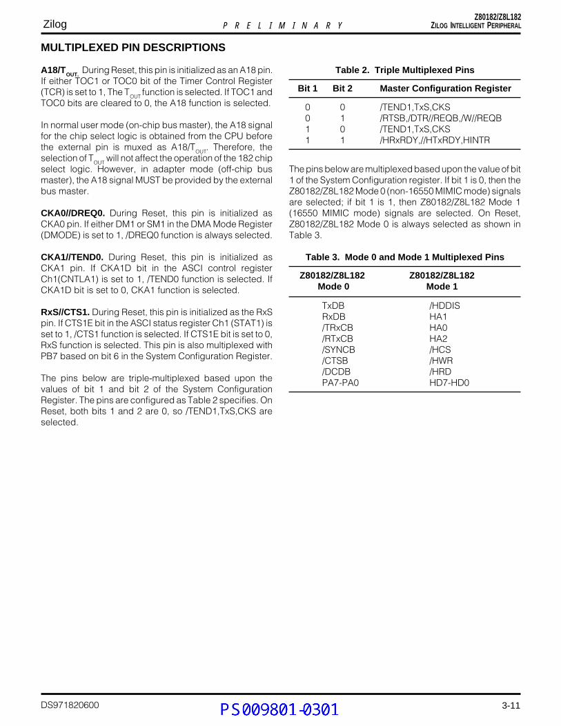
The pins below are triple-multiplexed based upon thevalues of bit 1 and bit 2 of the System ConfigurationRegister. The pins are configured as Table 2 specifies. OnReset, both bits 1 and 2 are 0, so /TEND1,TxS,CKS areselected.
Table 2. Triple Multiplexed Pins
Bit 1 Bit 2 Master Configuration Register
0 0 /TEND1,TxS,CKS0 1 /RTSB,/DTR//REQB,/W//REQB1 0 /TEND1,TxS,CKS1 1 /HRxRDY,//HTxRDY,HINTR
The pins below are multiplexed based upon the value of bit1 of the System Configuration register. If bit 1 is 0, then theZ80182/Z8L182 Mode 0 (non-16550 MIMIC mode) signalsare selected; if bit 1 is 1, then Z80182/Z8L182 Mode 1(16550 MIMIC mode) signals are selected. On Reset,Z80182/Z8L182 Mode 0 is always selected as shown inTable 3.
Table 3. Mode 0 and Mode 1 Multiplexed Pins
Z80182/Z8L182 Z80182/Z8L182 Mode 0 Mode 1
TxDB /HDDISRxDB HA1/TRxCB HA0/RTxCB HA2/SYNCB /HCS/CTSB /HWR/DCDB /HRDPA7-PA0 HD7-HD0
Gayle Gamble
PS009801-0301

3-12
Z80182/Z8L182ZILOG INTELLIGENT PERIPHERALP R E L I M I N A R YZilog
DS971820600
Ports B and C Multiplexed Pin Descriptions
Ports B and C are pin multiplexed with the Z180 ASCIfunctions and part of ESCC channel A. The MUX functionis controlled by bits 7-5 in the System Configuration Register.The MUX is organized as shown in Table 4.
Table 4. Multiplexed Port Pins
Port Mode ASCI/ESCC ModeFunction Function
PB7 RxS,/CTS1PB6 Select with bit 6=1 RxA1PB5 System Config Reg. TxA1PB4 RxA0PB3 TxA0PB2 Select with bit 5=1 /DCD0PB1 System Config Reg. /CTS0 (Note 1)PB0 /RTS0PC7 Always Reads /INT2 Ext.
StatusPC6 Always Reads /INT1 Ext.
StatusPC5 /W//REQAPC4 /SYNCAPC3 Select with bit 7=1 /DTR//REQAPC2 System Config Reg. /RTSA (Note 2)PC1 /CTSAPC0 /DCDA
Note 1:When the Port function (PB1) is selected, the internal Z180/CTS0 is always driven Low. This ensures that the ASCIchannel 0 of the Z180™ MPU is enabled to transmit data.
Note 2:Interrupt Edge /Pin MUX register, bit 3 chooses betweenthe /MWR or PC2//RTSA combination; the SystemConfiguration Register bit 7 chooses between PC2 and/RTSA.
Refer to Table 5 for the 1st, 2nd and 3rd pin functions.
Gayle Gamble
PS009801-0301

3-13
Z80182/Z8L182ZILOG INTELLIGENT PERIPHERALP R E L I M I N A R YZilog
DS971820600
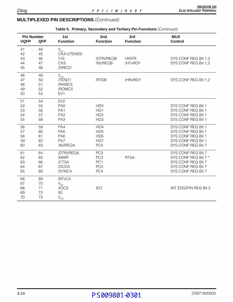
Table 5. Primary, Secondary and Tertiary Pin Functions
Pin Number 1st 2nd 3rd MUXVQFP QFP Function Function Function Control
1 4 ST2 5 A03 6 A14 7 A25 8 A3
6 9 A47 10 A58 11 A69 12 A710 13 A8
11 14 A912 15 A1013 16 A1114 17 A1215 18 VSS
16 19 A1317 20 A1418 21 A1519 22 A1620 23 A17
21 24 A18/TOUT
22 25 VDD
23 26 A1924 27 D025 28 D1
26 29 D227 30 D328 31 D429 32 D530 33 D6
31 34 D732 35 /RTS0 PB0 SYS CONF REG Bit 533 36 /CTS0 PB1 SYS CONF REG Bit 534 37 /DCD0 PB2 SYS CONF REG Bit 535 38 TxA0 PB3 SYS CONF REG Bit 5
36 39 RxA0 PB4 SYS CONF REG Bit 537 40 TxA1 PB5 SYS CONF REG Bit 638 41 RxA1 PB6 SYS CONF REG Bit 639 42 RxS//CTS1 PB7 SYS CONF REG Bit 640 43 CKA0//DREQ0
Gayle Gamble
PS009801-0301
3-14
Z80182/Z8L182ZILOG INTELLIGENT PERIPHERALP R E L I M I N A R YZilog
DS971820600
MULTIPLEXED PIN DESCRIPTIONS (Continued)
Table 5. Primary, Secondary and Tertiary Pin Functions (Continued)
Pin Number 1st 2nd 3rd MUXVQFP QFP Function Function Function Control
41 44 VSS
42 45 CKA1//TEND043 46 TxS /DTR//REQB HINTR SYS CONF REG Bit 1,244 47 CKS /W//REQB /HTxRDY SYS CONF REG Bit 1,245 48 /DREQ1
46 49 VDD
47 50 /TEND1 /RTSB /HRxRDY SYS CONF REG Bit 1,248 51 /RAMCS49 52 /ROMCS50 53 EV1
51 54 EV252 55 PA0 HD0 SYS CONF REG Bit 153 56 PA1 HD1 SYS CONF REG Bit 154 57 PA2 HD2 SYS CONF REG Bit 155 58 PA3 HD3 SYS CONF REG Bit 1
56 59 PA4 HD4 SYS CONF REG Bit 157 60 PA5 HD5 SYS CONF REG Bit 158 61 PA6 HD6 SYS CONF REG Bit 159 62 PA7 HD7 SYS CONF REG Bit 160 63 /W//REQA PC5 SYS CONF REG Bit 7
61 64 /DTR//REQA PC3 SYS CONF REG Bit 762 65 /MWR PC2 RTSA SYS CONF REG Bit 7 *63 66 /CTSA PC1 SYS CONF REG Bit 764 67 /DCDA PC0 SYS CONF REG Bit 765 68 /SYNCA PC4 SYS CONF REG Bit 7
66 69 /RTxCA67 70 VSS
68 71 /IOCS IEO INT EDG/PIN REG Bit 269 72 IEI70 73 VDD
Gayle Gamble
PS009801-0301

3-15
Z80182/Z8L182ZILOG INTELLIGENT PERIPHERALP R E L I M I N A R YZilog
DS971820600
Table 5. Primary, Secondary and Tertiary Pin Functions (Continued)
Pin Number 1st 2nd 3rd MUXVQFP QFP Function Function Function Control
71 74 RxDA72 75 /TRxCA73 76 TxDA74 77 /DCDB /HRD SYS CONF REG Bit 175 78 /CTSB /HWR SYS CONF REG Bit 1
76 79 TxDB /HDDIS SYS CONF REG Bit 177 80 /TRxCB HA0 SYS CONF REG Bit 178 81 RxDB HA1 SYS CONF REG Bit 179 82 /RTxCB HA2 SYS CONF REG Bit 180 83 /SYNCB /HCS SYS CONF REG Bit 1
81 84 /HALT82 85 /RFSH83 86 /IORQ84 87 /MRD /MREQ INT EDG/PIN REG Bit 385 88 E
86 89 /M187 90 /WR88 91 /RD89 92 PHI90 93 V
SS
91 94 XTAL92 95 EXTAL93 96 /WAIT94 97 /BUSACK95 98 /BUSREQ
96 99 /RESET97 100 /NMI98 1 /INT099 2 /INT1 PC6**100 3 /INT2 PC7**
Notes:* Also controlled by Interrupt Edge/Pin MUX Register** PC7 and PC6 are inputs only and can read values of /INT1 and /INT2.
Gayle Gamble
PS009801-0301

3-16
Z80182/Z8L182ZILOG INTELLIGENT PERIPHERALP R E L I M I N A R YZilog
DS971820600
Product Specification/Technical Manuals of each discreteproduct. The following subsections describe each of theindividual units of the Z182.
Z80182/Z8L182 FUNCTIONAL DESCRIPTION
Functionally, the on-chip Z182 MPU and ESCC™ are thesame as the discrete devices (Figure 1). Therefore, for adetailed description of each individual unit, refer to the
Z182 MPU FUNCTIONAL DESCRIPTION
This unit provides all the capabilities and pins of the ZilogZ8S180 MPU (Static Z80180 MPU). Figure 4 shows theS180 MPU Block Diagram of the Z182. This allows 100%
software compatibility with existing Z180™ (and Z80®)software. The following is an overview of the major functionalunits of the Z182.
Timing &Clock
Generator
Bus State Control Interrupt
CPU
DMACs(2)
16-BitProgrammableReload Timers
(2)
ClockedSerial I/O
Port AsynchronousSCI
(Channel 0)
AsynchronousSCI
(Channel 1)
MMU
Dat
a B
us (
8-B
it)
Add
ress
Bus
(16
-Bit)
/DREQ1/TEND
TxA0
CKA0 /DREQ0
RxA0
/RTS0
/CTS0
/DCD0
TxA1
CKA1 /TEND0
RxA1
Ø
A18 /TOUT
TxS
RxS//CTS
CKS
XT
AL
EX
TA
L
/RE
SE
T
/RD
/WR
/M1
/MR
EQ
/IOR
Q
/HA
LT
/WA
IT
/BU
SR
EQ
/BU
SA
CK
/RF
SH
ST
E /NM
I
/INT
0
/INT
1
/INT
2
A19-A0 D7-D0
Figure 4. S180 MPU Block Diagram of Z182
Gayle Gamble
PS009801-0301

3-17
Z80182/Z8L182ZILOG INTELLIGENT PERIPHERALP R E L I M I N A R YZilog
DS971820600
Z182 CPUThe Z182 CPU is 100% software compatible with the Z80®
CPU and has the following additional features:
Faster Execution Speed. The Z182 CPU is “fine tuned,”making execution speed, on average, 10% to 20% fasterthan the Z80 CPU.
Enhanced DRAM Refresh Circuit. Z182 CPU’s DRAMrefresh circuit does periodic refresh and generates an8-bit refresh address. It can be disabled or the refreshperiod adjusted, through software control.
Enhanced Instruction Set. The Z182 CPU has sevenadditional instructions to those of the Z80 CPU, whichinclude the MLT (Multiply) instruction.
HALT and Low Power Modes of Operation. The Z182CPU has HALT and Low Power modes of operation, whichare ideal for the applications requiring low powerconsumption like battery operated portable terminals.
System Stop Mode. When the Z182 is in System Stopmode, it is only the Z180 MPU that is in STOP mode.
Standby and Idle Mode. Please refer to the Z8S180Product Specification for additional information on thesetwo additional Low Power modes.
Instruction Set. The instruction set of the Z182 CPU isidentical to the Z180. For more details about eachtransaction, please refer to the Product Specification/Technical Manual for the Z180/Z80 CPU.
Z182 CPU Basic OperationZ182 CPU’s basic operation consists of the followingevents. These are identical to the Z180 MPU. For moredetails about each operation, please refer to the ProductSpecification/Technical Manual for the Z180.
Operation Code Fetch Cycle
Memory Read/Write Operation
Input/Output Operation
Bus Request/Acknowledge Operation
Maskable Interrupt Request Operation
Trap and Non-Maskable Interrupt Request Operation
HALT and Low Power Modes of Operation
Reset Operation
Memory Management Unit (MMU)The Memory Management Unit (MMU) allows the user tomap the memory used by the CPU (64 Kbytes of logicaladdressing space) into 1 Mbyte of physical addressingspace. The organization of the MMU allows object codecompatibility with the Z80 CPU while offering access to anextended memory space. This is accomplished by usingan effective common area-banked area scheme.
DMA ControllerThe Z182 MPU has two DMA controllers. Each DMAcontroller provides high-speed data transfers betweenmemory and I/O devices. Transfer operations supportedare memory-to-memory, memory-to/from-I/O, and I/O-to-I/O. Transfer modes supported are request, burst, andcycle steal. The DMA can access the full 1 Mbytesaddressing range with a block length up to 64 Kbytes andcan cross over 64K boundaries.
Asynchronous Serial Communication Interface(ASCI)This unit provides two individual full-duplex UARTs. Eachchannel includes a programmable baud rate generatorand modem control signals. The ASCI channels alsosupport a multiprocessor communication format.
Programmable Reload Timer (PRT)The Z182 MPU has two separate Programmable ReloadTimers, each containing a 16-bit counter (timer) and countreload register. The time base for the counters is systemclock divided by 20. PRT channel 1 provides an optionaloutput to allow for waveform generation.
Clocked Serial I/O (CSI/O)The CSI/O channel provides a half-duplex serial transmitterand receiver. This channel can be used for simple high-speed data connection to another CPU or MPU.
Programmable Wait State GeneratorTo ease interfacing with slow memory and I/O devices, theZ182 MPU unit has a programmable wait state generator.By programming the DMA/WAIT Control Register (DCNTL),up to three wait states are automatically inserted in memoryand I/O cycles. This unit also inserts wait states during on-chip DMA transactions. When using RAMCS and ROMCSwait state generators, the wait state controller with themost programmed wait states will determine the number ofwait states inserted.
Gayle Gamble
PS009801-0301

3-18
Z80182/Z8L182ZILOG INTELLIGENT PERIPHERALP R E L I M I N A R YZilog
DS971820600
Z85230 ESCC™ FUNCTIONAL DESCRIPTION
The Zilog Enhanced Serial Communication ControllerESCC™ is a dual channel, multiprotocol data communicationperipheral. The ESCC functions as a serial-to-parallel,parallel-to-serial converter/controller. The ESCC can besoftware-configured to satisfy a wide variety of serialcommunications applications. The device contains a varietyof new, sophisticated internal functions including on-chipbaud rate generators, digital phase-lock loops, and crystaloscillators, which dramatically reduce the need for externallogic.
The ESCC handles asynchronous formats, synchronousbyte-oriented protocols such as IBM® Bisync, andsynchronous bit-oriented protocols such as HDLC andIBM SDLC. This versatile device supports virtually anyserial data transfer application (telecommunication, LAN,etc.)
The device can generate and check CRC codes in anysynchronous mode and can be programmed to checkdata integrity in various modes. The ESCC also has facilitiesfor modem control in both channels in applications wherethese controls are not needed, the modem controls can beused for general-purpose I/O.
With access to 14 Write registers and 7 Read registers perchannel (number of the registers varies depending on theversion), the user can configure the ESCC to handle allsynchronous formats regardless of data size, number ofstop bits, or parity requirements. The ESCC alsoaccommodates all synchronous formats includingcharacter, byte, and bit-oriented protocols.
Within each operating mode, the ESCC also allows forprotocol variations by checking odd or even parity bits,character insertion or deletion, CRC generation, checkingbreak and abort generation and detection, and many otherprotocol-dependent features.
The ESCC (Enhanced SCC) is pin and software compatibleto the CMOS SCC version. The following enhancementswere made to the CMOS SCC:
Deeper Transmit FIFO (4 bytes)
Deeper Receive FIFO (8 bytes)
Programmable FIFO interrupt and DMA request level
Seven enhancements to improve SDLC link layersupports:- Automatic transmission of the opening flag- Automatic reset of Tx Underrun/EOM latch- Deactivation of /RTS pin after closing flag- Automatic CRC generator preset- Complete CRC reception- TxD pin automatically forced High with NRZI
encoding when using mark idle- Status FIFO handles better frames with an ABORT- Receive FIFO automatically unlocked for special
receive interrupts when using the SDLC status FIFO
Delayed bus latching for easier microprocessorinterface
New programmable features added with Write Register7' (WR seven prime)
Write registers, 3, 4, 5 and 10 are now readable
Read register 0 latched during access
DPLL counter output available as jitter-free transmitterclock source
Enhanced /DTR, /RTS deactivation timing
Gayle Gamble
PS009801-0301

3-19
Z80182/Z8L182ZILOG INTELLIGENT PERIPHERALP R E L I M I N A R YZilog
DS971820600
NRZ, NRZI or FM encoding/decoding. ManchesterCode Decoding (Encoding with External Logic).
Baud Rate Generator in each Channel
Digital Phase-Locked Loop (DPLL) for Clock Recovery
Crystal Oscillator
The following features are implemented in the ESCC™ forthe Z80182/Z8L182 only:
New 32-bit CRC-32 (Ethernet Polynomial)
ESCC Programmable Clock- programmed to be equal to system clock
divided by one or two- programmed by Z80182 Enhancement Register
Note: The ESCC™ programmable clock must beprogrammed to divide-by-two mode when operating abovethe following conditions:
– PHI > 20 MHz at 5.0V
– PHI > 10 MHz at 3.0V
The following features are common to both the ESCC andthe CMOS SCC:
Two independent full-duplex channels
Synchronous/Isochronous data rates:- Up to 1/4 of the PCLK using external clock source- Up to 5 Mbits/sec at 20 MHz PCLK (ESCC).
Asynchronous capabilities- 5, 6, 7 or 8 bits/character (capable of handling
4 bits/character or less)- 1, 1.5, or 2 stop bits- Odd or even parity- Times 1, 16, 32 or 64 clock modes- Break generation and detection- Parity, overrun and framing error detection
Byte oriented synchronous capabilities:- Internal or external character synchronization- One or two sync characters (6 or 8 bits/sync
character) in separate registers- Automatic Cyclic Redundancy Check (CRC)
generation/detection
SDLC/HDLC capabilities:- Abort sequence generation and checking- Automatic zero insertion and detection- Automatic flag insertion between messages- Address field recognition- I-field residue handling- CRC generation/detection- SDLC loop mode with EOP recognition/loop entry
and exit
Gayle Gamble
PS009801-0301

3-20
Z80182/Z8L182ZILOG INTELLIGENT PERIPHERALP R E L I M I N A R YZilog
DS971820600
Transmit Logic
Channel AReceive and Transmit Clock Multipexer
Transmit FIFO4 Bytes Transmit MUX
Data Encoding & CRC Generation
DigitalPhase-Locked
Loop
Baud RateGenerator
CrystalOscillatorAmplifier
Modem/Control Logic
Receive MUX
CRC Checker,Data Decode &Sync Character
Detection
Rec. Status* FIFO
Rec. Data* FIFO
SDLC Frame Status FIFO 10 x 19
Receive Logic
TxDA
/TRxCA
/RTxCA
/CTSA/DCDA/SYNCA/RTSA/DTRA//REQA
RxDA
Exploded View
InternalControlLogic
Channel ARegister
Channel BRegister
InterruptControlLogic
CPU & DMABus Interface
Databus
Control
Channel A
Channel B/INT/INTACK
IEIIEO
InterruptControl
* 8 bytes each
Figure 5. ESCC Block Diagram
Z85230 ESCC™ BLOCK DIAGRAM
For a detailed description of the Z85230 ESCC, refer to the ESCC Technical Manual. The following figure is the blockdiagram of the discrete ESCC, which was integrated into the Z182. The /INT line is internally connected to "INTO of theZ182.
Gayle Gamble
PS009801-0301

3-21
Z80182/Z8L182ZILOG INTELLIGENT PERIPHERALP R E L I M I N A R YZilog
DS971820600
The Z80182/Z8L182 has a 16550 MIMIC interface thatallows it to mimic the 16550 device. It has all the interfacepins necessary to connect to the PC/XT/AT bus. It containsthe complete register set of the part with the same interruptstructure. The data path allows parallel transfer of data toand from the register set by the internal Z80180 of theZ80182/Z8L182. There is no shift register associated withthe mimic of the 16550 UART. This interface saves theapplication from doing a serial transfer before performingdata compression or error correction on the data.
Control of the register set is maintained by six priorityencoded interrupts to the Z80182/Z8L182. When the PC/XT/AT writes to THR, MCR, LCR, DLL, DLM, FCR or readsthe RBR, an interrupt to the Z80182/Z8L182 is generated.Each interrupt can be individually masked off or all interruptscan be disabled by writing a single bit. Both mode 0 andmode 2 interrupts are supported by the 16550 MIMICinterface.
16550 MIMIC INTERFACE FUNCTIONAL DESCRIPTION
Two eight-bit timers are also available to control the datatransfer rate of the 16550 MIMIC interface. Their input istied to the ESCC channel B divide clock, so a down countof 24 bits is possible. An additional two eight bit timers areavailable for programming the FIFO timeout feature (FourCharacter Time Emulation) for both Receive and TransmitFIFO’s.
The 16550 MIMIC interface supports the PC/XT/AT interruptstructure as well as an additional mode that allows for awired Logic AND interrupt structure.
The 16550 MIMIC interface is also capable of high speedparallel DMA transfers by using two control lines and thetransmit and receive registers of the 16550 MIMIC interface.
All registers of the 16550 MIMIC interface are accessiblein any page of I/O space since only the lowest eightaddress lines are decoded. See Figure 6 for a blockdiagram of the 16550 MIMIC interface.
16550 MIMICRegister Set
4
8
16550 MIMIC Sideor PC Side Interface
PCAddr/Decode
PCDatabus
ReceiveTimer
TransmitTimer
Z80180IRQ
Control
MPU SideInterface
Control/Config
Register
Databus
Z80180Address
PC IRQ
DMAControl
8
Z80180Databus
6
PC DMA CNTL
2
Z80180DMA
Control
PC IRQ
2
1
Figure 6. 16550 MIMIC Block Diagram
Gayle Gamble
PS009801-0301

3-22
Z80182/Z8L182ZILOG INTELLIGENT PERIPHERALP R E L I M I N A R YZilog
DS971820600
16550 MIMIC FIFO DESCRIPTION
The receiver FIFO consists of a 16-word FIFO capable ofstoring eight data bits and three error bits for each characterstored (Figure 7). Parity error, Framing error and Breakdetect bits are stored along with the data bits by copyingtheir value from three shadow bits that are Write Only bitsfor the Z80180 MPU LSR address. The three shadow bitsare cleared after they are copied to the FIFO memory. InFIFO mode, to write error bits into the receiver FIFO, theMPU must first write the Parity, Framing and Break detectstatus to the Line Status Register (shadow bits) and thenwrite the character associated into the receiver buffer. Thedata and error bits will then move into the same address in
the FIFO. The error bits become available to the PC side ofthe interface when that particular location becomes thenext address to read (top of FIFO). At that time, they mayeither be read by the PC by accessing them in the LSR, orthey may cause an interrupt to the PC interface if soenabled. The error bits are set by the error status of the byteat the top of the FIFO, but may only be cleared by readingthe LSR. If successive reads of the receiver FIFO areperformed without reading the LSR, the status bits will beset if any of the bytes read have the respective error bit set.See Table 6 for the setting and clearing of the Line StatusRegister bits.
WRITE
BUFFER
16x8Data Bits
16x3ErrorBits
READ
BUFFER
WritePointer
ALU ReadPointer
Sync
Internal Clock
MPUCNTLLine
PC ReadLSRB2-B4
error33MPU Write
LSR ShadowB2-B4
8MPUDatabus(MPU Side Write)
Internal Clock
MPUIRQ
Sync
8
5
PC SideDatabus
(PC Side Read)
FIFO ControlRegister
PCIRQ
PCCntrlLine
Internal Clock
MPU SideInterface
16550 MIMIC orPC Side Interface
Figure 7. 16550 MIMIC Receiver FIFO Block Diagram
Gayle Gamble
PS009801-0301

3-23
Z80182/Z8L182ZILOG INTELLIGENT PERIPHERALP R E L I M I N A R YZilog
DS971820600
Table 6. 16550 Line Status Register
Error Description How to Set How to Clear
Error in At least one data byte available At least one error in receiver When there are no moreRCVR in FIFO with one error FIFO errorsFIFO
*TEMT Transmitter empty MPU writes a 1 MPU writes a 0
† *THRE Transmitter holding When MPU has When holding registerregister is empty read or emptied is not empty
the holding register
Break Break occurs when MPU writes 1 There is aDetect received data input PC-side read
is held in logic-0 of the LSRfor longer than afull word transmission
Framing Received character MPU writes 1 There is aError did not have a valid PC-side read
stop bit of the LSR
Parity Received character MPU writes 1 There is aError did not have correct PC-side read
even or odd parity of the LSR
Overrun Overlapping received MPU makes There is aError characters, thereby two writes PC-side read
destroying the to receiver of the LSRprevious character buffer register
†Data Indicates complete MPU writes to Empty ReceiverReady incoming data has RCVR FIFO or or Receiver FIFO
been received receiver bufferregister
Notes:* The TEMT and THRE bits take on different functions when
TEMT/Double Buffer mode is enabled.† These signals are delayed to HOST when using character
emulation delay.
Gayle Gamble
PS009801-0301

3-24
Z80182/Z8L182ZILOG INTELLIGENT PERIPHERALP R E L I M I N A R YZilog
DS971820600
16550 MIMIC FIFO DESCRIPTION (Continued)
The PC interface may be interrupted when 1, 4, 8 or 14bytes are available in the receiver FIFO by setting bits 6and 7 in the FCR (FIFO Control Register, PC address 02H)to the appropriate value. If the FIFO is not empty, but belowthe above trigger value, a timeout interrupt is available ifthe receiver FIFO is not written by the MPU or read by thePC from an interval determined by the Character TimeoutTimer. This is an additional Timer with MPU access onlythat is used to emulate the 16550 4 character timeoutdelay.
The Receive FIFO timeout timers are designed to reloadand begin countdown after every read or write of the RxFIFO, regardless of the Rx trigger level or number of bytesin the FIFO. Therefore, it is possible to get Timeout interruptsmore often than Receive data interrupts. In order to closelyemulate a 16550, a receive timeout timer enhancement isprovided. When enabling this feature, the timeout timer willnot begin counting down until the character emulationtimer for each byte of data in the Rx FIFO has expired.Note: Enabling this feature will facilitate increased16550 compatibility but may impede throughput. If theReceive Timeout interrupt occurs, the PC HOST will onlybe allowed to read up to 4-5 consecutive charactersbefore the Data Ready bit is forced to zero (even if thereis still more data in FIFO). This is required to maintaincharacter pacing.
READ
BUFFER
16x8Data Bits
WRITE
BUFFER
ReadPointer
ALU
Sync
Internal Clock
MPUCNTL
Line
8
MPUDatabus
(MPU Side Read)
FIFOControl Register
MPUIRQ
Sync
8PC SideDatabus(PC Side Write)
InternalClock
PCIRQ
PCCntrlLine
Internal Clock
MPU SideInterface
16550 MIMIC orPC Side Interface
WritePointer
5
The timer receives the ESCC /TRxCB as its input clock.Software must determine the correct values to programinto the Receiver Timeout register and the ESCC TRxCB toachieve the correct delay interval for timeout. Theseinterrupts are cleared by the FIFO reaching the triggerpoint or by resetting the Timeout Interval Timer by FIFOMPU write or PC read access.
With FIFO mode enabled, the MPU is interrupted when thereceiver FIFO is empty, corresponding to bit 5 being setin the IUS/IP register (MPU access only). This bitcorresponds to a PC read of the receive buffer in non-FIFO(16450) mode. The interrupt source is cleared when theFIFO becomes non-empty or the MPU reads the IUS/IPregister.
The transmitter FIFO is 16-byte FIFO with PC write andMPU read access (Figure 8). In FIFO mode, the PCreceives an interrupt when the transmitter becomes emptycorresponding to bit 5 being set in the LSR. This bit and theinterrupt source are cleared when the transmit FIFObecomes non-empty or the Interrupt Identification Register(IIR) register is read by the PC.
Figure 8. 16550 MIMIC Transmitter FIFO Block Diagram
Gayle Gamble
PS009801-0301

3-25
Z80182/Z8L182ZILOG INTELLIGENT PERIPHERALP R E L I M I N A R YZilog
DS971820600
On the MPU interface, the transmitted data available canbe programmed to interrupt the MPU on 1, 4, 8 or 14 bytesof available data by seeing the appropriate value in theMPU FSCR control register (MPU write only xxECH) bits 6and 7. A timeout feature exists, Transmit Timeout Timer,
Z80182/Z8L182 MIMIC SYNCHRONIZATION CONSIDERATIONS
Because of the asynchronous nature of the FIFO’s on theMIMIC, some synchronization plan must be provided toprevent conflict from the dual port accesses of the MPUand the PC.
To solve this problem, I/O to the FIFO is buffered and thebuffers allow both PC and MPU to access the FIFOasynchronously. Read and Write requests are thensynchronized by means of the MPU clock. Incoming signalsare buffered in such a way that metastable input levels arestabilized to valid 1 or 0 levels. Actual transfers to and fromthe buffers, from and to the FIFO memory, are timed by theMPU clock. ALU evaluation is performed on a differentphase than the transfer to ensure stable pointer values.
Another potential problem is that of simultaneous accessof the MPU and PC to any of the various ‘mailbox’ typeregisters. This is solved by dual buffering of the variousread/write registers. During a read access by either theMPU or PC to a mailbox register, the data in the output orslave portion of the buffered register is not permitted tochange. Any write that might take place during this timewill be stored in the input of master part of the register. Thecorresponding status/interrupt is reset appropriately basedon the write having followed the read to the register. Forexample, the IUS/IP bit for the LCR write will not be clearedby the MPU read of the LCR if a simultaneous write to theLCR by the PC takes place. Instead the LSR data willchange after the read access and IUS/IP bit 3 remains atlogic 1.
which is an additional 8-bit timer with SCC TxRCB as theinput source. If the transmitter FIFO is non-empty and noPC write or MPU read of the FIFO has taken place within thetimer interval, a timeout occurs causing a correspondinginterrupt to the MPU.
Gayle Gamble
PS009801-0301

3-26
Z80182/Z8L182ZILOG INTELLIGENT PERIPHERALP R E L I M I N A R YZilog
DS971820600
Z80182 MIMIC DOUBLE BUFFERING FOR THE TRANSMITTER
The Z80182 Rev DA implements double buffering for thetransmitter in 16450 mode and sets the TEMT bit in the LSRRegister automatically.
When this feature is enabled and character delay emulationis being used (see Figure 9):
1. The PC THRE bit in the LSR Register is set when theTHR Register is empty;
2. PC Host writes to the 16450 THR Register;
3. Whenever the Z80182 TSR buffer is empty and onecharacter delay timer is in a timed-out state, the bytefrom the THR Register is transferred to the TSR buffer;the timer is in timed-out state after FIFO Reset or afterHost TEMT is set. This allows a dual write to THR whenHost TEMT is set.
4. Restart character delay timer (timer reloads and countsdown) with byte transfer from THR Register to the TSRbuffer;
5. Whenever the TSR buffer is full, the TEMT bit in MPULSR Register is reset with no delay;
6. MPU reads TSR buffer;
7. TEMT bit in LSR Register for MPU is set with no delaywhenever the TSR buffer is empty;
8. When the TSR buffer is read by MPU and THR Registeris empty and one character delay timer reaches zero,the TEMT bit in the LSR Register for Host is set from 0to 1.
The PC THRE bit in the LSR Register is reset whenever theTHR Register is full and set whenever THR Register isempty.
MPU IREQ and DMA Request for the transmit data istrigger whenever TSR buffer is full and cleared wheneverTSR buffer is empty.
If character delay emulation is not used the TEMT bit in theLSR Register is set whenever both the THR Register andthe TSR buffer are both empty. The Host TEMT bit is clearif there is data in either the TSR buffer of THR Register.
16450THR
Register
Host Write
Empty/FullHost & MPU THRE = 1 0
Byte Transfer if:- THRE=0;- TSR = 1;- Character delay timer is timed out.
Note: Timer reloads and counts down whenever data is transferred from THR to TSR.
THR to TSRdelay
transfer
TSRTransmitShift Reg.Emulation
Empty/Full(MPU TEMT) TSRE = 1 0
Host TEMT = 1 if - THRE = 1 - TSRE = 1 - Emulation delay timer is timed out
Note: MPU sees TSR bit in the LSR Register as TEMT bit
Added TSR Buffer for thetransmit data
Figure 9. TEMT Emulation Logic Implementation
Gayle Gamble
PS009801-0301

3-27
Z80182/Z8L182ZILOG INTELLIGENT PERIPHERALP R E L I M I N A R YZilog
DS971820600
PROGRAMMING
The following subsections explain and define theparameters for I/O Address assignments. The three tablesin this section describe the mapping of the commonregisters shared by the MPU and the 16550 MIMIC. TheMPU address refers to the I/O address as accessed fromthe MPU side (the Z180™ MPU interface side of the 16550MIMIC). Note that only the lowest eight address lines aredecoded for Z182 peripheral access. The full sixteen
address lines are decoded for on-chip Z180 MPU access.The PC address (coined because the UART is common inPCs) is the address needed to access the MIMIC registersthrough the MIMIC interface signals. The MIMIC interfacesignals are multiplexed with the ESCC channel B and thePort A signals, and must be activated through the SystemConfiguration Register and the Interrupt Edge/Pin MUXRegister.
Table 7. Z80182/Z8L182 MPU Registers
Register Name MPU Addr PC Addr
Z80182/Z8L182 MPU Control Registers 0000H to 00x3FH None(Relocatable to 0040H to 007FHor 0080H to 00BFH)
PARALLEL PORTS FUNCTIONAL DESCRIPTION
The Z80182/Z8L182 has three 8-bit bi-directional Ports.Each bit is individually programmable for input or output(with the exception of PC6 and PC7 which are inputs only).
The Ports are controlled through two registers: the PortDirection Control Register and the Port Data Register.(Please see register description for Ports A, B and C).
Note:“x” indicates don’t care condition
Table 8. Z80182/Z8L182 MIMIC Register MAP
Register Name MPU Addr/Access PC Addr/Access
MMC MIMIC Master Control Register xxFFH R/W NoneIUS/IP Interrupt Pending xxFEH R/Wb7 NoneIE Interrupt Enable xxFDH R/W NoneIVEC Interrupt Vector xxFCH R/W NoneTTCR Transmit Time Constant xxFAH R/W NoneRTCR Receive Time Constant xxFBH R/W NoneFSCR FIFO Status and Control xxECH R/W7-4 NoneRTTC Receive Timeout Time Constant xxEAH R/W NoneTTTC Transmit Timeout Time Constant xxEBH R/W NoneRBR Receive Buffer Register xxF0H W only 00H DLAB=0 R onlyTHR Transmit Holding Register xxF0H R only 00H DLAB=0 W onlyIER Interrupt Enable Register xxF1H R only 01H DLAB=0 R/WIIR Interrupt Identification None 02H R onlyFCR FIFO Control Register xxE9H R only 02H W onlyMM REGISTER XXE9H W only NoneLCR Line Control Register xxF3H R only 03H R/WMCR Modem Control Register xxF4H R only 04H R/WLSR Line Status Register xxF5H R/Wb6432 05H R onlyMSR Modem Status Register xxF6H R/Wb7-4 06H R onlySCR Scratch Register xxF7H R only 07H R/WDLL Divisor Latch (LSByte) xxF8H R only 00H DLAB=1 R/WDLM Divisor Latch (MSByte) xxF9H R only 01H DLAB=1 R/W
Gayle Gamble
PS009801-0301

3-28
Z80182/Z8L182ZILOG INTELLIGENT PERIPHERALP R E L I M I N A R YZilog
DS971820600
PROGRAMMING (Continued)
Table 9. Z80182/Z8L182 ESCC, PIA and MISC Registers
Register Name MPU Addr/Access PC Addr/Access
WSG Chip Select Register xxD8H R/W NoneZ80182 Enhancements Register xxD9H R/W NonePC Data Direction Register xxDDH R/W NonePC Data Register xxDEH R/W NoneInterrupt Edge/Pin MUX Control xxDFH R/W NoneESCC Chan A Control Register xxE0H R/W NoneESCC Chan A Data Register xxE1H R/W NoneESCC Chan B Control Register xxE2H R/W NoneESCC Chan B Data Register xxE3H R/W NonePB Data Direction Register xxE4H R/W NonePB Data Register xxE5H R/W NoneRAMUBR RAM Upper Boundary Register xxE6H R/W NoneRAMLBR RAM Lower Boundary Register xxE7H R/W NoneROM Address Boundary Register xxE8H R/W NonePA Data Direction Register xxEDH R/W NonePA Data Register xxEEH R/W NoneSystem Configuration Register xxEFH R/W None
Gayle Gamble
PS009801-0301

3-29
Z80182/Z8L182ZILOG INTELLIGENT PERIPHERALP R E L I M I N A R YZilog
DS971820600
Z182 MPU CONTROL REGISTERS
Figures 10 through 50 refer to the Z80182/Z8L182 MPUControl registers. For additional information, refer to theZ8S180 Product Specification and Technical Manual.
ASCI CHANNELS CONTROL REGISTERS
MPE RE TE /RTS0MPBR/
EFR MOD2 MOD1 MOD0
0
R/W
0
R/W
0
R/W
1
R/W
x
R/W
0
R/W
0
R/W
0
R/W
Bit
Upon RESET
R/W
CNTLA0
MODE Selection
Addr 00H
Read - Multiprocessor Bit ReceiveWrite - Error Flag Reset
Request To Send
Transmit Enable
Receive Enable
Multiprocessor Enable
0 0 0 Start + 7-Bit Data + 1 Stop0 0 1 Start + 7-Bit Data + 2 Stop0 1 0 Start + 7-Bit Data + Parity + 1 Stop0 1 1 Start + 7-Bit Data + Parity + 2 Stop1 0 0 Start + 8-Bit Data + 1 Stop1 0 1 Start + 8-Bit Data + 2 Stop1 1 0 Start + 8-Bit Data + Parity + 1 Stop1 1 1 Start + 8-Bit Data + Parity + 2 Stop
Figure 10a. ASCI Control Register A (Ch. 0)
Gayle Gamble
PS009801-0301

3-30
Z80182/Z8L182ZILOG INTELLIGENT PERIPHERALP R E L I M I N A R YZilog
DS971820600
ASCI CHANNELS CONTROL REGISTERS (Continued)
MPE RE TE CKA1D MPBR/EFR
MOD2 MOD1 MOD0
0
R/W
0
R/W
0
R/W
1
R/W
x
R/W
0
R/W
0
R/W
0
R/W
Bit
Upon RESET
R/W
CNTLA1
MODE Selection
Addr 01H
Read - Multiprocessor Bit ReceiveWrite - Error Flag Reset
CKA1 Disable
Transmit Enable
Receive Enable
Multiprocessor Enable
0 0 0 Start + 7-Bit Data + 1 Stop0 0 1 Start + 7-Bit Data + 2 Stop0 1 0 Start + 7-Bit Data + Parity + 1 Stop0 1 1 Start + 7-Bit Data + Parity + 2 Stop1 0 0 Start + 8-Bit Data + 1 Stop1 0 1 Start + 8-Bit Data + 2 Stop1 1 0 Start + 8-Bit Data + Parity + 1 Stop1 1 1 Start + 8-Bit Data + Parity + 2 Stop
Figure 10b. ASCI Control Register A (Ch. 1)
Gayle Gamble
PS009801-0301

3-31
Z80182/Z8L182ZILOG INTELLIGENT PERIPHERALP R E L I M I N A R YZilog
DS971820600
MPBT MP /CTS/PS
SS2 SS1 SS0
Invalid
R/W
0
R/W
†
R/W
0
R/W
0
R/W
1
R/W
1
R/W
1
R/WR/W
CNTLB0
Clock Source and Speed Select
Addr 02H
Bit
Upon Reset
DRPE0
Divide Ratio
Parity Even or Odd
Clear To Send/Prescale
Multiprocessor
Multiprocessor Bit Transmit
† /CTS - Depending on the condition of /CTS pin. PS - Cleared to 0.
General PS = 0 PS = 1Divide Ratio (Divide Ratio = 10) (Divide Ratio = 30)
SS, 2, 1, 0 DR = 0 (x16) DR = 1 (x64) DR = 0 (x16) DR = 1 (x64)
000 Ø ÷ 160 Ø ÷ 640 Ø ÷ 480 Ø ÷ 1920001 Ø ÷ 320 Ø ÷ 1280 Ø ÷ 960 Ø ÷ 3840010 Ø ÷ 640 Ø ÷ 2580 Ø ÷ 1920 Ø ÷ 7680011 Ø ÷ 1280 Ø ÷ 5120 Ø ÷ 3840 Ø ÷ 15360100 Ø ÷ 2560 Ø ÷ 10240 Ø ÷ 7680 Ø ÷ 30720101 Ø ÷ 5120 Ø ÷ 20480 Ø ÷ 15360 Ø ÷ 61440110 Ø ÷ 10240 Ø ÷ 40960 Ø ÷ 30720 Ø ÷ 122880111 External Clock (Frequency < Ø ÷ 40)
Figure 11. ASCI Control Register B (Ch. 0)
Gayle Gamble
PS009801-0301

3-32
Z80182/Z8L182ZILOG INTELLIGENT PERIPHERALP R E L I M I N A R YZilog
DS971820600
ASCI CHANNELS CONTROL REGISTERS (Continued)
MPBT MP /CTS/PS
SS2 SS1 SS0
Invalid
R/W
0
R/W
0
R/W
0
R/W
0
R/W
1
R/W
1
R/W
1
R/WR/W
CNTLB1
Clock Source and Speed Select
Addr 03H
Bit
Upon Reset
DRPE0
Divide Ratio
Parity Even or Odd
Read - Status of /CTS pinWrite - Select PS
Multiprocessor
Multiprocessor Bit Transmit
General PS = 0 PS = 1Divide Ratio (Divide Ratio = 10) (Divide Ratio = 30)
SS, 2, 1, 0 DR = 0 (x16) DR = 1 (x64) DR = 0 (x16) DR = 1 (x64)
000 Ø ÷ 160 Ø ÷ 640 Ø ÷ 480 Ø ÷ 1920001 Ø ÷ 320 Ø ÷ 1280 Ø ÷ 960 Ø ÷ 3840010 Ø ÷ 640 Ø ÷ 2580 Ø ÷ 1920 Ø ÷ 7680011 Ø ÷ 1280 Ø ÷ 5120 Ø ÷ 3840 Ø ÷ 15360100 Ø ÷ 2560 Ø ÷ 10240 Ø ÷ 7680 Ø ÷ 30720101 Ø ÷ 5120 Ø ÷ 20480 Ø ÷ 15360 Ø ÷ 61440110 Ø ÷ 10240 Ø ÷ 40960 Ø ÷ 30720 Ø ÷ 122880*111 External Clock (Frequency < Ø ÷ 40)
Note:* Baud rate is external clock rate ÷ 16; therefore, Ø ÷ (40 x 16)
is maximum baud rate using external clocking.
Figure 12. ASCI Control Register B (Ch. 1)
Gayle Gamble
PS009801-0301

3-33
Z80182/Z8L182ZILOG INTELLIGENT PERIPHERALP R E L I M I N A R YZilog
DS971820600
Upon Reset
RDRF OVRN /DCD0 TDRE TIE
0
R
0
R
0
R
0
R
0
R/W R
††
R
0
R/WR/W
STAT0
Transmit Interrupt Enable
Addr 04H
Bit RIEFE
Transmit Data RegisterEmpty
Data Carrier Detect
Receive Interrupt Enable
Framing Error
Parity Error
PE
†
Over Run Error
Receive Data Register Full
† /DCD0 - Depending on the condition of /DCD0 Pin.
†† /CTS0 Pin TDRE
L 1 H 0
Figure 13. ASCI Status Register
RDRF OVRN CTS1E TDRE TIE
0
R
0
R
0
R
0
R
0
R/W R/W
1
R
0
R/WR/W
STAT1
Transmit Interrupt Enable
Addr 05H
Bit
Upon Reset
RIEFE
Transmit Data RegisterEmpty
/CTS1 Enable
Receive Interrupt Enable
Framing Error
Parity Error
PE
0
Over Run Error
Receive Data Register Full
Figure 14. ASCI Status Register (Ch. 1)
Gayle Gamble
PS009801-0301
3-34
Z80182/Z8L182ZILOG INTELLIGENT PERIPHERALP R E L I M I N A R YZilog
DS971820600
7 6 5 4 3 2 1 0
Break feature bit0 = dissolve1 = enable
BRK0Read/Write Addr 12H
Break detect bit0 = no break1 = break
Break generate bit0 = no break1 = break
ASCI CHANNELS CONTROL REGISTERS (Continued)
Figure 15. ASCI Transmit Data Register (Ch. 0)
7 6 5 4 3 2 1 0
Transmit Data
TDR0Write Only Addr 06H
x x x x x x x x
Received Data
TSR1Read Only Addr 09H
Figure 18. ASCI Receive Data Register (Ch. 1)
Figure 16. ASCI Transmit Data Register (Ch. 1)
7 6 5 4 3 2 1 0
Transmit Data
TDR1Write Only Addr 07H
x x x x x x x x
Received Data
TSR0Read Only Addr 08H
Figure 17. ASCI Receive Data Register (Ch. 0)
Figure 19. ASCI Break Control Register (Ch. 0)
7 6 5 4 3 2 1 0
Break feature enable bit0 = disable1 = enable
BRK1Read/Write Addr 13H
Break detect bit0 = no break1 = break
Break generate bit0 = no break1 = break
Figure 20. ASCI Break Control Register (Ch. 1)
Gayle Gamble
PS009801-0301

3-35
Z80182/Z8L182ZILOG INTELLIGENT PERIPHERALP R E L I M I N A R YZilog
DS971820600
CSI/O REGISTERS
EF EIE SS2 SS1 SS0
0R
0R/W
0R/W
0R/W
1 1R/W
1R/W
1R/WR/W
Speed Select
Addr 0AH
Bit
Upon Reset-TE
Transmit Enable
Receive Enable
End Interrupt Enable
End Flag
RE
CNTR
SS2, 1, 0 Baud Rate
000 Ø ÷ 20001 Ø ÷ 40010 Ø ÷ 80011 Ø ÷ 100
Figure 21. CSI/O Control Register
SS2, 1, 0 Baud Rate
100 Ø ÷ 320101 Ø ÷ 640110 Ø ÷ 1280111 External Clock
(Frequency < Ø ÷ 20)
7 6 5 4 3 2 1 0
Read - Received DataWrite - Transmit Data
TRDRRead/Write Addr 0BH
Figure 22. CSI/O Transmit/Receive Data Register
Gayle Gamble
PS009801-0301
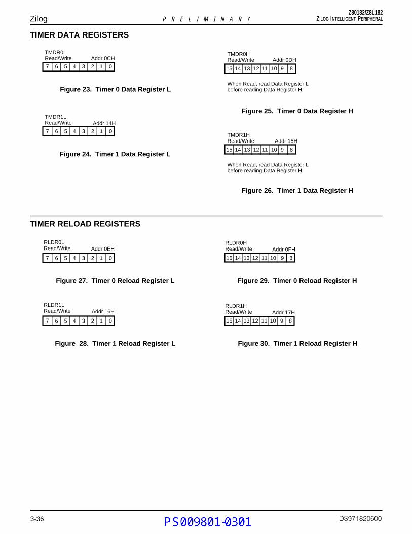
3-36
Z80182/Z8L182ZILOG INTELLIGENT PERIPHERALP R E L I M I N A R YZilog
DS971820600
TIMER DATA REGISTERS
7 6 5 4 3 2 1 0
TMDR0LRead/Write Addr 0CH
Figure 23. Timer 0 Data Register L
7 6 5 4 3 2 1 0
TMDR1LRead/Write Addr 14H
Figure 24. Timer 1 Data Register L
15 14 13 12 11 10 9 8
TMDR0HRead/Write Addr 0DH
When Read, read Data Register L before reading Data Register H.
Figure 25. Timer 0 Data Register H
15 14 13 12 11 10 9 8
TMDR1HRead/Write Addr 15H
When Read, read Data Register L before reading Data Register H.
Figure 26. Timer 1 Data Register H
TIMER RELOAD REGISTERS
7 6 5 4 3 2 1 0
RLDR0LRead/Write Addr 0EH
Figure 27. Timer 0 Reload Register L
15 14 13 12 11 10 9 8
RLDR0HRead/Write Addr 0FH
Figure 29. Timer 0 Reload Register H
7 6 5 4 3 2 1 0
RLDR1LRead/Write Addr 16H
Figure 28. Timer 1 Reload Register L
15 14 13 12 11 10 9 8
RLDR1HRead/Write Addr 17H
Figure 30. Timer 1 Reload Register H
Gayle Gamble
PS009801-0301
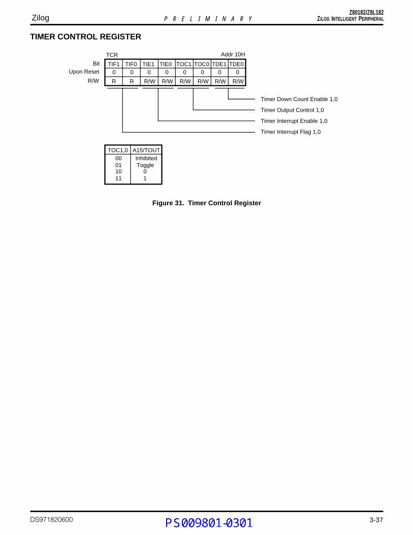
3-37
Z80182/Z8L182ZILOG INTELLIGENT PERIPHERALP R E L I M I N A R YZilog
DS971820600
TIMER CONTROL REGISTER
TIF1 TIF0 TOC0 TDE1 TDE00
R
0
R
0
R/W
0
R/W
0
R/W R/W
0
R/W
0
R/WR/W
TCR
Timer Down Count Enable 1,0
Addr 10H
BitUpon Reset
TOC1TIE0
Timer Output Control 1,0
Timer Interrupt Enable 1,0
Timer Interrupt Flag 1,0
TIE10
TOC1,0 A15/TOUT00 Inhibited01 Toggle10 011 1
Figure 31. Timer Control Register
Gayle Gamble
PS009801-0301

3-38
Z80182/Z8L182ZILOG INTELLIGENT PERIPHERALP R E L I M I N A R YZilog
DS971820600
FREE RUNNING COUNTER
CPU CONTROL REGISTER
7 6 5 4 3 2 1 0
FRCRead Only Addr 18H
Figure 32. Free Running Counter
Figure 33. CPUNote: See Figure 49 for full description.
0 0 0 0 0 0 0 0
CPU Control Register (CCR)
D7 D6 D5 D4 D3 D2 D1 D0
Addr 1FH
DMA REGISTERS
SAR0LRead/Write Addr 20HSA7 SA0
SAR0HRead/Write Addr 21HSA15 SA8
SAR0BRead/Write Addr 22H
SA16SA19
-- - -
Bits 0-2 (3) are used for SAR0B
A19,
xxxx
A18,
xxxx
A17,
0011
A16
0101
DMA Transfer Request
/DREQ0 (external)RDR0 (ASCI0)RDR1 (ASCI1)Not Used
Figure 34. DMA 0 Source Address Registers
Gayle Gamble
PS009801-0301

3-39
Z80182/Z8L182ZILOG INTELLIGENT PERIPHERALP R E L I M I N A R YZilog
DS971820600
DMA REGISTERS
DAR0LRead/Write Addr 23HDA7 DA0
DAR0HRead/Write Addr 24HDA15 DA8
DAR0BRead/Write Addr 25H
DA16DA19
-- - -
Bits 0-2 (3) are used for DAR0B
A19,
xxxx
A18,
xxxx
A17,
0011
A16
0101
DMA Transfer Request
/DREQ0 (external)TDR0 (ASCI0)TDR1 (ASCI1)Not Used
Figure 35. DMA 0 Destination Address Registers
BCR0LRead/Write Addr 26HBC7 BC0
BCR0HRead/Write Addr 27HBC15 BC8
Figure 36. DMA 0 Byte Counter Registers
MAR1LRead/Write Addr 28HMA7 MA0
MAR1HRead/Write Addr 29HMA15 MA8
MAR1BRead/Write Addr 2AH
MA16MA19
-- - -
Figure 37. DMA 1 Memory Address Registers
BCR1LRead/Write Addr 2EHBC7 BC0
BCR1HRead/Write Addr 2FHBC15 BC8
Figure 39. DMA 1 Byte Count Registers
IAR1LRead/Write Addr 2BHIA7 IA0
IAR1HRead/Write Addr 2CHIA15 IA8
Figure 38. DMA I/O Address Registers
Gayle Gamble
PS009801-0301

3-40
Z80182/Z8L182ZILOG INTELLIGENT PERIPHERALP R E L I M I N A R YZilog
DS971820600
DMA REGISTERS (Continued)
DE1 DE0 DIE0 - DIME0
R/W
0
R/W
1
W1W
0 0R/W
1 0RR/W
DMA Master Enable
Addr 30HBit
Upon ResetDIE1/DWE0
DMA Interrupt Enable 1, 0
DMA Enable Bit Write Enable 1, 0
DMA Enable Ch 1, 0
/DWE1
DSTAT
R/W
Figure 40. DMA Status Register
- - SM0 MMOD -
1 1 0
R/W
0
R/W
0 0
R/W
0 1
R/W
Memory MODE Select
Addr 31HBit
Upon Reset
SM1DM0
Ch 0 Source Mode 1, 0
Ch 0 Destination Mode 1, 0
DM1
DMODE
R/W R/W
DM1, 000011011
DestinationMMMI/O
AddressDAR0+1DAR0-1
DAR0 FixedDAR0 Fixed
SM1, 000011011
SourceMMMI/O
AddressSAR0+1SAR0-1
SAR0 FixedSAR0 Fixed
01
Mode
Cycle Steal ModeBurst Mode
MMOD
Figure 41. DMA Mode Registers
Gayle Gamble
PS009801-0301

3-41
Z80182/Z8L182ZILOG INTELLIGENT PERIPHERALP R E L I M I N A R YZilog
DS971820600
MWI1 MWI0 DMS0 DIM1 DIM0
1 1 1
R/W
1
R/W
0 0
R/W
0 0
R/W
DMA Ch 1 I/O MemoryMode Select
Addr 32H
Bit
Upon Reset
DMS1IWI0
/DREQi Select, i = 1, 0
I/0 Wait Insertion
IWI1
DCNTL
R/W R/WR/WR/W R/W
Memory Wait Insertion
DM1, 0
00011011
Transfer Mode
M - I/OM - I/OI/O - MI/O - M
Address Increment/Decrement
DMSi
10
Sense
Edge SenseLevel Sense
MWI1, 0
00011011
No. of Wait States
0123
IWI1, 0
00011011
No. of Wait States
1234
MAR1+1MAR1-1
IAR1 FixedIAR1 Fixed
IAR1 FixedIAR1 FixedMAR1+1MAR1-1
*
Note:* If using ROM/RAM Chip Select wait state generators, the Z180 wait state generator should be set to 0.
Figure 42. DMA/WAIT Control Register
Gayle Gamble
PS009801-0301

3-42
Z80182/Z8L182ZILOG INTELLIGENT PERIPHERALP R E L I M I N A R YZilog
DS971820600
MMU REGISTERS
CB7 CB6 CB2 CB1 CB0
0 0 0
R/W
0
R/W
0 0
R/W
0 0
R/W
MMU Common Base Register
Addr 38H
Bit
Upon Reset
CB3CB4CB5
CBR
R/W R/WR/WR/W R/W
Figure 43. MMU Common Base Register
BB7 BB6 BB2 BB1 BB0
0 0 0
R/W
0
R/W
0 0
R/W
0 0
R/W
MMU Bank Base Register
Addr 39H
Bit
Upon Reset
BB3BB4BB5
BBR
R/W R/WR/WR/W R/W
Figure 44. MMU Bank Base Register
CA3 CA2 BA2 BA1 BA0
1 1 1
R/W
1
R/W
0 0
R/W
0 0
R/W
MMU Bank Area Register
Addr 3AH
Bit
Upon Reset
BA3CA0CA1
CBAR
R/W R/WR/WR/W R/W
MMU Common Area Register
Figure 45. MMU Common/Bank Area Register
Gayle Gamble
PS009801-0301

3-43
Z80182/Z8L182ZILOG INTELLIGENT PERIPHERALP R E L I M I N A R YZilog
DS971820600
SYSTEM CONTROL REGISTERS
IL7 IL6 - - -
0 0 0
R/W
0 0 0 0 0
R/W
Interrupt Vector Low
Addr 33H
Bit
Upon Reset
--IL5
IL
R/WR/W
Figure 46. Interrupt Vector Low Register
TRAP UFO ITE2 ITE1 ITE0
0 0 1 1 1 0R/W
0 1R/W
/INT Enable 2, 1, 0
Addr 34H
Bit
Upon Reset
---
ITC
R/WRR/W R/W
Undefined Fetch Object
TRAP
Figure 47. INT/TRAP Control Register
REFE REFW - CYC1 CYC01 1 1 1 1 1 0 0
R/W
Cycle Select
Addr 36H
Bit
Upon Reset
--
Refresh Wait State
Refresh Enable
-
RCR
R/WR/WR/W R/W
CYC1, 0
00011011
Interval of Refresh Cycle
10 states20 states40 states80 states
Figure 48. Refresh Control Register
Gayle Gamble
PS009801-0301

3-44
Z80182/Z8L182ZILOG INTELLIGENT PERIPHERALP R E L I M I N A R YZilog
DS971820600
SYSTEM CONTROL REGISTERS (Continued)
M1E /M1TE - - -
1 1 1 1 1 1 1 1
R/W
I/O Compatibility
Addr 3EH
Bit
Upon Reset
--
/M1 Temporary Enable
/M1 Enable
/IOC
OMCR
WR/W R/W
Note:This register should be programmed to 0x0xxxxxb(x = don't care) as a part of Initialization.
Figure 49. Operation Mode Control Register
IOA7 IOA6 - - -
0 0 0 1 1 1 1 1
R/W
I/O Stop
Addr 3FH
Bit
Upon Reset
--
I/O AddressCombination of 11is reserved
IOSTP
ICR
R/WR/W R/W
Figure 50. I/O Control Register
Gayle Gamble
PS009801-0301

3-45
Z80182/Z8L182ZILOG INTELLIGENT PERIPHERALP R E L I M I N A R YZilog
DS971820600
ADDITIONAL FEATURES ON THE Z182 MPU
The following is a detailed description of the enhancementsto the Z8S180 from the standard Z80180 in the areas ofSTANDBY, IDLE, and STANDBY-QUICK RECOVERYmodes.
Add-On FeaturesThere are five different power-down modes. SLEEP andSYSTEM STOP are inherited from the Z80180. In SLEEPmode, the CPU is in a stopped state while the on-chip
I/Os are still operating. In I/O STOP mode, the on-chip I/Osare in a stopped state while leaving the CPU running. InSYSTEM STOP mode, both the CPU and the on-chip I/Osare in the stopped state to reduce the current consumption.The Z8S180 has added two additional power-down modes,STANDBY and IDLE, to reduce the current consumptioneven further. The differences among these power-downmodes are summarized in Table 10.
Table 10. Power Down Modes
Power-Down CPU On-Chip Recovery Recovery TimeModes Core I/O OSC. CLKOUT Source (Minimum)
SLEEP Stop Running Running Running RESET, Interrupts 1.5 ClockI/O STOP Running Stop Running Running By Programming -SYSTEM STOP Stop Stop Running Running RESET, Interrupts 1.5 ClockIDLE† Stop Stop Running Stop RESET, Interrupts, BUSREQ 8 +1.5 ClockSTANDBY† Stop Stop Stop Stop RESET, Interrupts, BUSREQ 217 +1.5 Clock (Normal Recovery)
26 +1.5 Clock (Quick Recovery)
Notes:† IDLE and STANDBY modes are only offered in Z8S180. Note that theminimum recovery time can be achieved if INTERRUPT is used as theRecovery Source.
STANDBY ModeThe Z8S180 has been designed to save power. Two low-power programmable power-down modes have beenadded; STANDBY mode and IDLE mode. TheSTANDBY/IDLE mode is selected by multiplexing D6 andD3 of the CPU Control Register (CCR, I/O Address = 1FH).To enter STANDBY mode:
1. Set D6 and D3 to 1 and 0, respectively.
2. Set the I/O STOP bit (D5 of ICR,I/O Address = 3FH) to 1.
3. Execute the SLEEP instruction.
When the part is in STANDBY mode, it behaves similar tothe SYSTEM STOP mode which currently exists on theZ80180, except that the STANDBY mode stops the externaloscillator, internal clocks and reduces power consumptionto typically 50 µA..
Since the clock oscillator has been stopped, a restart ofthe oscillator requires a period of time for stabilization. An
18-bit counter has been added in the Z8S180 to allow foroscillator stabilization. When the part receives an externalIRQ or BUSREQ during STANDBY mode, the oscillator isrestarted and the timer counts down 217 counts beforeacknowledgment is sent to the interrupt source.
The recovery source needs to remain asserted for durationof the 217 count, otherwise standby will be resumed.
The following is a description of how the part exits STANDBYfor different interrupts and modes of operation.
STANDBY Mode Exit with /RESETThe /RESET input needs to be asserted for a duration longenough for the crystal oscillator to stabilize and then exitfrom the STANDBY mode. When /RESET is de-asserted, itgoes through the normal reset timing to start instructionexecution at address (logical and physical) 0000H.
The clocking is resumed within the Z8S180 and at thesystem clock output after /RESET is asserted when thecrystal oscillator is restarted, but not yet stabilized.
Gayle Gamble
PS009801-0301

3-46
Z80182/Z8L182ZILOG INTELLIGENT PERIPHERALP R E L I M I N A R YZilog
DS971820600
If an External Maskable Interrupt input is asserted, the CPUresponds according to the status of the Global InterruptEnable Flag IEF1 (determined by the ITE1 bit) and thesettings of the corresponding interrupt enable bit in theInterrupt/Trap Control Register (ITC: I/O Address = 34H):
a. If an interrupt source is disabled in the ITC, assertingthe corresponding interrupt input would not cause theZ8S180 to exit STANDBY mode. This is true regardlessof the state of the Global Interrupt Enable Flag IEF1.
b. If the Global Interrupt Flag IEF1 is set to 1, and if aninterrupt source is enabled in the ITC, asserting thecorresponding interrupt input causes the Z8S180 toexit STANDBY mode. The CPU performs an interruptacknowledge sequence appropriate to the input beingasserted when clocking is resumed if:
- The interrupt input follows the normal interruptdaisy chain protocol.
- The interrupt source is active until the acknowledgecycle is completed.
c. If the Global Interrupt Flag IEF1 is disabled, i.e., resetto 0, and if an interrupt source is enabled in the ITC,asserting the corresponding interrupt input will stillcause the Z8S180 to exit STANDBY mode. The CPUwill proceed to fetch and execute instructions thatfollow the SLEEP instruction when clocking is resumed.
If the External Maskable Interrupt input is not active untilclocking resumes, the Z8S180 will not exit STANDBYmode. If the Non-Maskable Interrupt (/NMI) is not activeuntil clocking resumes, the Z8S180 still exits the STANDBYmode even if the interrupt sources go away before thetimer times out, because /NMI is edge-triggered. Thecondition is latched internally once /NMI is asserted Low.
IDLE ModeIDLE mode is another power-down mode offered by theZ8S180. To enter IDLE mode:
1. Set D6 and D3 to 0 and 1, respectively.
2. Set the I/O STOP bit (D5 of ICR,I/O Address = 3FH) to 1.
3. Execute the SLEEP instruction.
STANDBY Mode Exit with BUS REQUESTOptionally, if the BREXT bit (D5 of CPU Control Register)is set to 1, the Z8S180 exits STANDBY mode when the/BUSREQ input is asserted; the crystal oscillator is thenrestarted. An internal counter automatically provides timefor the oscillator to stabilize, before the internal clockingand the system clock output of the Z8S180 are resumed.
The Z8S180 relinquishes the system bus after the clockingis resumed by:
- Tri-State the address outputs A19 through A0.
- Tri-State the bus control outputs /MREQ, /IORQ,/RD and /WR.
- Asserting /BUSACK
The Z8S180 regains the system bus when /BUSREQ isdeactivated. The address outputs and the bus controloutputs are then driven High; the STANDBY mode isexited.
If the BREXT bit of the CPU Control Register (CCR) iscleared, asserting the /BUSREQ would not cause theZ8S180 to exit STANDBY mode.
If STANDBY mode is exited due to a reset or an externalinterrupt, the Z8S180 remains relinquished from the systembus as long as /BUSREQ is active.
STANDBY Mode Exit with ExternalInterruptsSTANDBY mode can be exited by asserting input /NMI.The STANDBY mode may also exit by asserting /INT0,/INT1 or /INT2, depending on the conditions specified inthe following paragraphs.
/INT0 wake-up requires assertion throughout duration ofclock stabilization time (217 clocks).
If exit conditions are met, the internal counter providestime for the crystal oscillator to stabilize, before the internalclocking and the system clock output within the Z8S180are resumed.
1. Exit with Non-Maskable Interrupts
If /NMI is asserted, the CPU begins a normal NMI interruptacknowledge sequence after clocking resumes.
2. Exit with External Maskable Interrupts
Gayle Gamble
PS009801-0301

3-47
Z80182/Z8L182ZILOG INTELLIGENT PERIPHERALP R E L I M I N A R YZilog
DS971820600
When the part is in IDLE mode, the clock oscillator is keptoscillating, but the clock to the rest of the internal circuit,including the CLKOUT, is stopped completely. IDLE modeis exited in a similar way as STANDBY mode, i.e., RESET,BUS REQUEST or EXTERNAL INTERRUPTS, except thatthe 217 bit wake-up timer is bypassed; all control signals areasserted eight clock cycles after the exit conditions aregathered.
STANDBY-QUICK RECOVERY ModeSTANDBY-QUICK RECOVERY mode is an option offeredin STANDBY mode to reduce the clock recovery time inSTANDBY mode from 217 clock cycles (6.5 ms at 20 MHz)to 26 clock cycles (3.2 µs at 20 MHz). This feature can onlybe used when providing an oscillator as clock source.
To enter STANDBY-QUICK RECOVERY mode:
1. Set D6 and D3 to 1 and 1, respectively.
2. Set the I/O STOP bit (D5 of ICR,I/O Address = 3FH) to 1.
3. Execute the SLEEP instruction.
When the part is in STANDBY-QUICK RECOVERY mode,the operation is identical to STANDBY mode except whenexit conditions are gathered, i.e., RESET, BUS REQUESTor EXTERNAL INTERRUPTS; the clock and other controlsignals are recovered sooner than the STANDBY mode.
Note: If STANDBY-QUICK RECOVERY is enabled, theuser must make sure stable oscillation is obtained within64 clock cycles.
CPU Control RegisterThe Z8S180 has an additional register which allows theprogrammer to select options that directly affect the CPUperformance as well as controlling the STANDBY operatingmode of the chip. The CPU Control Register (CCR) allowsthe programmer to change the divide-by-two internal clockto divide-by-one. In addition, applications where EMI noiseis a problem, the Z8S180 can reduce the output drivers onselected groups of pins to 25% of normal pad drivercapability which minimizes the EMI noise generated by thepart.
D7 D6 D5 D4 D3 D2 D1 D0
LNCPUCTL 0 = Standard Drive 1 = 25% Drive On CPU Control Signals
CPU Control Register (CCR) Addr 1FH
LNAD/DATA 0 = Standard Drive 1 = 25% Drive On A19-A0, D7-D0
Reserved
Standby/Idle Enable 00 = No Standby 01 = Idle After Sleep 10 = Standby After Sleep 11 = Standby After Sleep 64 Cycle Exit (Quick Recovery) LNPHI
0 = Standard Drive 1 = 25% Drive On EXT.PHI Clock
BREXT 0 = Ignore BUSREQ In Standby/Idle 1 = Standby/Idle Exit on BUSREQ
Clock Divide 0 = XTAL/2 1 = XTAL/1
0 0 0 0 0 0 0 0
Figure 51. CPU Control Register
Gayle Gamble
PS009801-0301
3-48
Z80182/Z8L182ZILOG INTELLIGENT PERIPHERALP R E L I M I N A R YZilog
DS971820600
CPU Control Register
Bit 7. Clock Divide Select. Bit 7 of the CCR allows theprogrammer to set the internal clock to divide the externalclock by 2 if the bit is 0 and divide-by-one if the bit is 1.Upon reset, this bit is set to 0 and the part is individe-by-two mode. Since the on-board oscillator is notguaranteed to operate above 20 MHz, an external sourcemust be used to achieve the maximum 33 MHz operationof the part, i.e., an external clock at 66 MHz with 50% dutycycle.
If an external oscillator is used in divide-by-one mode, theminimum pulse width requirement must be satisfied.
Bits 6 and 3. STANDBY/IDLE Enable. These two bits areused for enabling/disabling the IDLE and STANDBY mode.
Setting D6, D3 to 0 and 1, respectively, enables the IDLEmode. In the IDLE mode, the clock oscillator is keptoscillating but the clock to the rest of the internal circuit,including the CLKOUT, is stopped. The Z8S180 entersIDLE mode after fetching the second opcode of a SLEEPinstruction, if the I/O STOP bit is set.
Setting D6, D3 to 1 and 0, respectively, enables theSTANDBY mode. In the STANDBY mode, the clockoscillator is stopped completely. The Z8S180 entersSTANDBY after fetching the second opcode of a SLEEPinstruction, if the I/O STOP bit is set.
Setting D6, D3 to 1 and 1, respectively, enables theSTANDBY-QUICK RECOVERY mode. In this mode, itsoperations are identical to STANDBY except that the clock
recovery is reduced to 64 clock cycles after the exitconditions are gathered. Similarly, in STANDBY mode, theZ8S180 enters STANDBY after fetching the second opcodeof a SLEEP instruction, if the I/O STOP bit is set.
Bit 5. BREXT. This bit controls the ability of the Z8S180 tohonor a bus request during STANDBY mode. If this bit isset to 1 and the part is in STANDBY mode, a BUSREQ ishonored after the clock stabilization timer is timed out.
Bit 4. LNPHI. This bit controls the drive capability on thePHI Clock output. If this bit is set to 1, the PHI Clock outputis reduced to 25% of its drive capability.
Bit 2. Reserved
Bit 1. LNCPUCTL. This bit controls the drive capability ofthe CPU Control pins. When this bit is set to 1, the outputdrive capability of the following pins is reduced to 25% ofthe original drive capability:
- /BUSACK - /MREQ- /RD - /IORQ- /WR - /RFSH- /M1 - /HALT- E - /TEND1
Bit 0. LNAD/DATA. This bit controls the drive capability ofthe Address/Data bus output drivers. If this bit is set to 1,the output drive capability of the Address and Data busoutput is reduced to 25% of its original drive capability.
Gayle Gamble
PS009801-0301

3-49
Z80182/Z8L182ZILOG INTELLIGENT PERIPHERALP R E L I M I N A R YZilog
DS971820600
Z85230 ESCC™ CONTROL REGISTERS
See Figures 52 and 53 for the ESCC Control registers. Foradditional information, refer to the ESCC ProductSpecification /Technical Manual.
The Z80182/Z8L182 has two ESCC channels. They can beaccessed in any page of I/O space since only the lowesteight address lines are decoded for access. Their Z180™
MPU Address locations are shown in Table 11.
When the 16550 MIMIC interface is enabled, ESCC channelB is disconnected from the output pins. The channel B/TRxCB clock is connected to the Transmit and Receivetimers of the 16550 MIMIC interface. It is recommendedthat /TRxCB be programmed as an output with properbaud rate values to timeout the transmitter and receiverof the 16550 MIMIC interface.
Table 11. ESCC Control and Data Map
ESCC Channel A Control Z180 MPU Address xxE0HData Z180 MPU Address xxE1H
ESCC Channel B Control Z180 MPU Address xxE2HData Z180 MPU Address xxE3H
Gayle Gamble
PS009801-0301

3-50
Z80182/Z8L182ZILOG INTELLIGENT PERIPHERALP R E L I M I N A R YZilog
DS971820600
PROGRAMMING THE ESCC™
The ESCC contains write registers in each channel that areprogrammed by the system separately to configure thefunctional uniqueness of the channels.
In the ESCC, the data registers are directly addressed byselecting a High on the D//C pin. With all other registers(with the exception of WR0 and RR0), programming thewrite registers requires two write operations and readingthe read registers, both a write and a read operation. Thefirst write is to WR0 and contains three bits that point to theselected register. The second write is the actual controlword for the selected read register accessed. All of theESCC registers, including the data registers, may beaccessed in this fashion. The pointer bits are automaticallycleared after the read or write operation so that WR0 (orRR0) is addressed again.
With the Z80182/Z8L182, a new feature is implemented inthe ESCC. The Transmitter and Receiver is now capable ofsending and comparing a 32-bit CRC-32 (EthernetPolynomial):
x32 + x26 +x23 +x22 + x16 + x12 + x11 +x10 + x8 + x7 + x5 + x4 +x2 + x + 1
This feature is enabled by access to WR7' Bit 7, whichselects the 32-bit CRC polynomial for the transmitter andreceiver and overrides any selection of SDLC/CRC-16CRCs. When the 32-bit CRC override feature is enabled,the transmitter will only send 32-bit CRC when CRC is to besent. On the receive side, the CRC comparison/calculationwill be done only on 32-bit CRC values. The result of the32-bit CRC comparison will be maintained in RR1 bit D6 inplace of the 16-bit CRC comparison result. The 32-bit CRCcompare result will also be maintained in the 10x19 FIFOfor frames in which 32-bit CRC is enabled. The CRC stillcan be preset to all 0s or all 1s. 32-bit CRC is disabled uponpower-up or reset.
Note: The ESCC cannot do simultaneous calculation/comparison using both 16-bit and 32-bit CRC.
Also, for the Z80182/Z8L182 only, the clock provided to theESCC core is equal to the system clock divided by 1 or 2.The divider is programmed in the Z80182 EnhancementRegister bit 3.
Divide-by-two should be programmed when running theZ182 beyond:
- 20 MHz, 5V- 10 MHz, 3V
Note: Upon power-up or reset the system clock is equal tothe ESCC clock.
Initialization. The system program first issues a series ofcommands to initialize the basic mode of operation. Thisis followed by other commands to qualify conditions withinthe selected mode. For example, in the Asynchronousmode, character length, clock rate, number of stop bits,and even or odd parity should be set first. Then theinterrupt mode is set, and finally, the receiver and transmitterare enabled.
Write Registers. The ESCC contains 16 write registers (17counting the transmit buffer) in each channel. These writeregisters are programmed separately to configure thefunctional "personality" of the channels. There are tworegisters (WR2 and WR9) shared by the two channels thatare accessed through either of them. WR2 contains theinterrupt vector for both channels, while WR9 contains theinterrupt control bits and reset commands. A new register,WR7', was added to the ESCC and may be written to ifWR15, D0 is set. Figure 50 shows the format of each writeregister.
Read Registers. The ESCC contains ten read registers(eleven, counting the receive buffer (RR8) in each channel).Four of these may be read to obtain status information(RR0, RR1, RR10, and RR15). Two registers (RR12 andRR13) are read to learn the baud rate generator timeconstant. RR2 contains either the unmodified interruptvector (channel A) or the vector modified by statusinformation (channel B). RR3 contains the Interrupt Pending(IP) bits (channel A only). RR6 and RR7 contain theinformation in the SDLC Frame Status FIFO, but is onlyread when WR15, D2 is set. If WR7' D6 is set, WriteRegisters WR3, WR4, WR5, WR7, and WR10 can be readas RR9, RR4, RR5, and RR14, respectively. Figure 51shows the format of each Read register.
Gayle Gamble
PS009801-0301

3-51
Z80182/Z8L182ZILOG INTELLIGENT PERIPHERALP R E L I M I N A R YZilog
DS971820600
CONTROL REGISTERS
D7 D6 D5 D4 D3 D2 D1 D0
0 0 0 Register 00 0 1 Register 10 1 0 Register 20 1 1 Register 31 0 0 Register 41 0 1 Register 51 1 0 Register 61 1 1 Register 70 0 0 Register 80 0 1 Register 90 1 0 Register 100 1 1 Register 111 0 0 Register 121 0 1 Register 131 1 0 Register 141 1 1 Register 15
With Point High Command
*
*
Write Register 0 (non-multiplexed bus mode)
0 0 0 Null Code0 0 1 Point High0 1 0 Reset Ext/Status Interrupts0 1 1 Send Abort (SDLC)1 0 0 Enable Int on Next Rx Character1 0 1 Reset Tx Int Pending1 1 0 Error Reset1 1 1 Reset Highest IUS
0 0 Null Code0 1 Reset Rx CRC Checker1 0 Reset Tx CRC Generator1 1 Reset Tx Underrun/EOM Latch
D7 D6 D5 D4 D3 D2 D1 D0
V0
Write Register 2
V1
V2
V3
V4
V5
V6
V7
InterruptVector
D7 D6 D5 D4 D3 D2 D1 D0
Write Register 1
Ext Int Enable
Tx Int Enable
Parity is Special Condition
0 0 Rx Int Disable0 1 Rx Int On First Character or Special Condition1 0 Int On All Rx Characters or Special Condition1 1 Rx Int On Special Condition Only
WAIT/DMA Request OnReceive//Transmit
/WAIT/DMA Request Function
WAIT/DMA Request Enable
D7 D6 D5 D4 D3 D2 D1 D0
Write Register 4
Parity Enable
0 0 X1 Clock Mode0 1 X16 Clock Mode1 0 X32 Clock Mode1 1 X64 Clock Mode
Parity EVEN//ODD
0 0 Sync Modes Enable0 1 1 Stop Bit/Character1 0 1 1/2 Stop Bits/Character1 1 2 Stop Bits/Character
0 0 8-Bit Sync Character0 1 16-Bit Sync Character1 0 SDLC Mode (01111110 Flag)1 1 External Sync Mode
Figure 52. Write Register Bit Functions
D7 D6 D5 D4 D3 D2 D1 D0
Write Register 3
Rx Enable
0 0 Rx 5 Bits/Character0 1 Rx 7 Bits/Character1 0 Rx 6 Bits/Character1 1 Rx 8 Bits/Character
Sync Character Load Inhibit
Address Search Mode (SDLC)
Rx CRC Enable
Enter Hunt Mode
Auto Enables
Gayle Gamble
PS009801-0301

3-52
Z80182/Z8L182ZILOG INTELLIGENT PERIPHERALP R E L I M I N A R YZilog
DS971820600
CONTROL REGISTERS (Continued)
D7 D6 D5 D4 D3 D2 D1 D0
Write Register 5
Tx CRC Enable
0 0 Tx 5 Bits(Or Less)/Character0 1 Tx 7 Bits/Character1 0 Tx 6 Bits/Character1 1 Tx 8 Bits/Character
RTS
/SDLC/CRC-16
Tx Enable
Send Break
DTR
D7 D6 D5 D4 D3 D2 D1 D0
Write Register 6
Sync3Sync3Sync3 1ADR3 x
Sync2Sync2Sync2 1ADR2 x
Sync1Sync1Sync1 1ADR1 x
Sync0Sync0Sync0 1ADR0 x
Monosync, 8 BitsMonosync, 6 BitsBisync, 16 BitsBisync, 12 BitsSDLCSDLC (Address Range)
Sync4Sync4Sync4Sync0ADR4ADR4
Sync5Sync5Sync5Sync1ADR5ADR5
Sync6Sync0Sync6Sync2ADR6ADR6
Sync7Sync1Sync7Sync3ADR7ADR7
D7 D6 D5 D4 D3 D2 D1 D0
Write Register 7
Sync3Sync1Sync11Sync7 1
Sync2Sync0Sync10Sync6 1
Sync1 xSync9Sync5 1
Sync0 xSync8Sync4 0
Monosync, 8 BitsMonosync, 6 BitsBisync, 16 BitsBisync, 12 BitsSDLC
Sync4Sync2Sync12Sync8 1
Sync5Sync3Sync13Sync9 1
Sync6Sync4Sync14Sync10 1
Sync7Sync5Sync15Sync11 0
Figure 52. Write Register Bit Functions (Continued)
Gayle Gamble
PS009801-0301

3-53
Z80182/Z8L182ZILOG INTELLIGENT PERIPHERALP R E L I M I N A R YZilog
DS971820600
D7 D6 D5 D4 D3 D2 D1 D0
Auto Tx Flag
WR 7' Prime
Auto EOM Reset
Auto RTS Deactivation
Rx FIFO Int Level
DTR/REQ Timing Mode
Tx FIFO Int Level
Extended Read Enable
32-bit CRC Enable
D7 D6 D5 D4 D3 D2 D1 D0
Write Register 10
6-Bit//8-Bit Sync
0 0 NRZ0 1 NRZI1 0 FM1 (Transition = 1)1 1 FM0 (Transition = 0)
Loop Mode
Abort//Flag On Underrun
Mark//Flag Idle
Go Active On Poll
CRC Preset I//O
D7 D6 D5 D4 D3 D2 D1 D0
Write Register 11
0 0 /TRxC Out = Xtal Output0 1 /TRxC Out = Transmit Clock1 0 /TRxC Out = BR Generator Output1 1 /TRxC Out = DPLL Output
/TRxC O/I
0 0 Transmit Clock = /RTxC Pin0 1 Transmit Clock = /TRxC Pin1 0 Transmit Clock = BR Generator Output1 1 Transmit Clock = DPLL Output
0 0 Receive Clock = /RTxC Pin0 1 Receive Clock = /TRxC Pin1 0 Receive Clock = BR Generator Output1 1 Receive Clock = DPLL Output
/RTxC Xtal//No Xtal
D7 D6 D5 D4 D3 D2 D1 D0
Write Register 9
VIS
0 0 No Reset0 1 Not used1 0 Channel Reset 1 1 Force Hardware Reset
NV
DLC
MIE
Status High//Status Low
Software INTACK Enable
Figure 52. Write Register Bit Functions (Continued)
Gayle Gamble
PS009801-0301

3-54
Z80182/Z8L182ZILOG INTELLIGENT PERIPHERALP R E L I M I N A R YZilog
DS971820600
CONTROL REGISTERS (Continued)
D7 D6 D5 D4 D3 D2 D1 D0
TC0
Write Register 12
TC1
TC2
TC3
TC4
TC5
TC6
TC7
Lower Byte of Time Constant
D7 D6 D5 D4 D3 D2 D1 D0
Write Register 14
0 0 0 Null Command0 0 1 Enter Search Mode0 1 0 Reset Missing Clock0 1 1 Disable DPLL1 0 0 Set Source = BR Generator1 0 1 Set Source = /RTxC1 1 0 Set FM Mode1 1 1 Set NRZI Mode
BR Generator Enable
BR Generator Source
/DTR/Request Function
Auto Echo
Local Loopback
D7 D6 D5 D4 D3 D2 D1 D0
TC8
Write Register 13
TC9
TC10
TC11
TC12
TC13
TC14
TC15
Upper Byte of Time Constant
D7 D6 D5 D4 D3 D2 D1 D0
WR7' SDLC Feature Enable
Write Register 15
Zero Count IE
SDLC FIFO Enable
DCD IE
Sync/Hunt IE
CTS IE
Tx Underrun/EOM IE
Break/Abort IE
Figure 52. Write Register Bit Functions (Continued)
Gayle Gamble
PS009801-0301

3-55
Z80182/Z8L182ZILOG INTELLIGENT PERIPHERALP R E L I M I N A R YZilog
DS971820600
D7 D6 D5 D4 D3 D2 D1 D0
0
Read Register 3
0
0
Ext/Status IP
Tx IP
Rx IP
0
0
D7 D6 D5 D4 D3 D2 D1 D0
Rx Character Available
Read Register 0
Zero Count
Tx Buffer Empty
DCD
Sync/Hunt
CTS
Tx Underrun/EOM
Break/Abort
D7 D6 D5 D4 D3 D2 D1 D0
All Sent
Read Register 1
Residue Code 2
Residue Code 1
Residue Code 0
Parity Error
Rx Overrun Error
CRC/Framing Error
End of Frame (SDLC)
D7 D6 D5 D4 D3 D2 D1 D0
BC0
Read Register 6*
BC1
BC2
BC3
BC4
BC5
BC6
BC7
*Can only be accessed if the SDLC FIFO enhancement is enabled (WR15 bit D2 set to 1)
SDLC FIFO Status and Byte Count (LSB)
D7 D6 D5 D4 D3 D2 D1 D0
V0
Read Register 2
V1
V2
V3
V4
V5
V6
V7
InterruptVector
D7 D6 D5 D4 D3 D2 D1 D0
BC8
Read Register 7*
BC9
BC10
BC11
BC12
BC13
FDA: FIFO Data Available1 = Status Reads from FIFO0 = Status Reads from EMSCC
*Can only be accessed if the SDLC FIFO enhancement is enabled (WR15 bit D2 set to 1)
SDLC FIFO Status and Byte Count (LSB)
FOS: FIFO Overflow Status1 = FIFO Overflowed0 = Normal
Figure 52. Write Register Bit Functions (Continued)
Gayle Gamble
PS009801-0301

3-56
Z80182/Z8L182ZILOG INTELLIGENT PERIPHERALP R E L I M I N A R YZilog
DS971820600
CONTROL REGISTERS (Continued)
D7 D6 D5 D4 D3 D2 D1 D0
0
Read Register 10
On Loop
0
0
Loop Sending
0
Two Clocks Missing
One Clock Missing
D7 D6 D5 D4 D3 D2 D1 D0
TC8
Read Register 13
TC9
TC10
TC11
TC12
TC13
TC14
TC15
Upper Byteof Time Constant
D7 D6 D5 D4 D3 D2 D1 D0
TC0
Read Register 12
TC1
TC2
TC3
TC4
TC5
TC6
TC7
Lower Byteof Time Constant
D7 D6 D5 D4 D3 D2 D1 D0
0
Read Register 15
Zero Count IE
SDLC Status FIFO Enable
DCD IE
Sync/Hunt IE
CTS IE
Tx Underrun/EOM IE
Break/Abort IE
Figure 53. Read Register Bit Functions
Gayle Gamble
PS009801-0301

3-57
Z80182/Z8L182ZILOG INTELLIGENT PERIPHERALP R E L I M I N A R YZilog
DS971820600
Z182 MISCELLANEOUS CONTROL AND INTERFACE REGISTERS
Figures 54 through 65 describe miscellaneous registersthat control the Z182 configuration, RAM/ROM chip select,interrupt and various status and timers.
System Configuration Register
Bit 7 Port C SelectWhen this bit is set to 1, bit 8 parallel Port C is selected onthe multiplexed pins. When this bit is reset to 0 then thesemultiplexed pins take ESCC™ Channel A functions.
Bit 6 PB7-PB5 SelectWhen this bit is set to 1, parallel Port B bits 7 through 5 areselected on the multiplexed pins. When this bit is reset to0, these multiplexed pins become RxA1, TxA1 and RxS/CTS1.
Bit 5 PB4-PB0 SelectWhen this bit is set to 1, parallel Port B bits 4 through 0 areselected on the multiplexed pins. When this bit is reset to0, these multiplexed pins take ASCI channel 0 functions.
Bit 4 DDOUT
ROM Emulator Mode EnableWhen this bit is set to 1, the Z182 is in “ROM emulatormode”. In this mode, bus direction for certain transactionperiods are set to the opposite direction to export internalbus transactions outside the Z80182/Z8L182. This allowsthe use of ROM emulators/logic analyzers for applicationdevelopment (see Tables 12a and 12b).
Note: The word “Out” means that the Z182 data busdirection is in output mode, “In” means input mode, and “Z”means high impedance. DD
OUT stands for Data Direction
Out and is the status of the D4 bit in the System ConfigurationRegister (SCR).
Figure 54. System Configuration Register(Z180 MPU Read/Write, Address xxEFH)
0 0 0 0 0 0 0 0
D7 D6 D5 D4 D3 D2 D1 D0
Daisy Chain0=ESCC > 16550 MIMIC1=16550 MIMIC> ESCC
ESCC/MIMIC0=ESCC Channel B1=16550 MIMIC Interface
Tri-Muxed Pins0=Z801801=ESCC Channel/16550 MIMIC
Disable ROMs0=ROM Sel Enabled1=ROM Sel Disabled
DOUT0=No Data Out1=Data Out
Port PB4-PB0 Select0=ASCI Channel 0 Func1=PB4-PB0 Selected
Port PB7-PB5 Select0=RXA1, TXA1, (RXS,/CTS1)1=PB7-PB5 Selected
Port C Select0=ESCC Channel A Func1=Port C Selected
Table 12a. Data Bus Direction (Z182 Bus Master)I/O And Memory Transactions
I/O Write I/O Read I/O Write I/O Read Write Read Z80182to On-Chip From On-Chip to Off-Chip From Off-Chip To From /Z8L182Peripherals Peripherals Peripherals Peripherals Memory Mode Refresh Idle Mode
Z80182 Out Z Out In Out In Z Z/Z8L182Data Bus(DD
OUT =0)
Z80182 Out Out Out In Out In Z Z/Z8L182Data Bus(DD
OUT =1)
Gayle Gamble
PS009801-0301
3-58
Z80182/Z8L182ZILOG INTELLIGENT PERIPHERALP R E L I M I N A R YZilog
DS971820600
Z182 MISCELLANEOUS CONTROL AND INTERFACE REGISTERS
Table 12b. Data Bus Direction (Z182 Bus Master)Interrupt Acknowledge Transaction
Intack For Intack ForOn-Chip Off-Chip
Peripheral (IEI=1) Peripheral (IEI=0)
Z80182/Z8L182Data Bus Z In(DD
OUT=0)
Z80182/Z8L182Data Bus Out In(DD
OUT=1)
Table 13a. Data Bus Direction (Z80182/Z8L182 is not Bus Master)I/O And Memory Transactions
I/O Write I/O Read I/O Write I/O Read Write Readto On-Chip From On-Chip to Off-Chip From Off-Chip To From Z80182Peripherals Peripherals Peripherals Peripherals Memory Mode Refresh Idle Mode
Z80182 In Out Z Z Z In Z Z/Z8L182Data BusDD
OUT=0)
Z80182 In Out Z Z Z In Z Z/Z8L182Data Bus(DD
OUT=1)
Table 13b. Data Bus Direction (Z80182/Z8L182 is not Bus Master)Interrupt Acknowledge Transaction
Intack For Intack ForOn-Chip Off-Chip
Peripheral Peripheral
Z80182/Z8L182Data Bus Out In(DD
OUT=0)
Z80182/Z8L182Data Bus Out In(DD
OUT=1)
Gayle Gamble
PS009801-0301

3-59
Z80182/Z8L182ZILOG INTELLIGENT PERIPHERALP R E L I M I N A R YZilog
DS971820600
Z182 MISCELLANEOUS CONTROL AND INTERFACE REGISTERS
Bit 3 Disable ROMsIf this bit is 1, it disables the ROMCS pin. If it is 0, addressesbelow the ROM boundary set by the ROMBR register willcause the ROMCS pin to go Low.
Bit 2 Tri-Muxed Pins SelectThe Z80182/Z8L182 has three pins that are triplemultiplexed and controlled by bit 2 and bit 1. Table 14shows the different modes.
Table 14. SCR Control for Triple Multiplexed Pins
Bit 2 Bit 1 System Configuration Register
0 0 /TEND1,TxS,CKS 0 1 /TEND1,TxS,CKS 1 0 /RTSB,(/DTR//REQB),(/W//REQB) 1 1 /HRxRDY,//HTxRDY,HINTR
Bit 1 ESCC ™ Channel B/MIMICIf this bit is 0, Mode 0 is selected.If this bit is 1, Mode 1 is selected.
Mode 0:Channel A ESCC EnabledChannel B ESCC EnabledPIA Port Enabled16550 MIMIC Interface Disabled
Mode 1:Channel A ESCC enabledChannel B outputs disabledPIA disabled16550 MIMIC Interface Enabled
Bit 0 Daisy ChainThis bit is used to set interrupt priority of the ESCC and16550 MIMIC interface. If it is 0, the ESCC is higher up inthe daisy chain than the 16550 MIMIC interface. If it is 1, the16550 interface is higher up than the ESCC. Note that/INT0 is used for both MIMIC and ESCC Interrupts.
/RAMCS AND /ROMCS REGISTERS
To assist decoding of ROM and RAM blocks of memory,three more registers and two pins have been added to the
Z80182/Z8L182. The two pins are /ROMCS and /RAMCS.The three registers are RAMUBR, RAMLBR and ROMBR.
1 1 1 1 1 1 1 1
D7 D6 D5 D4 D3 D2 D1 D0
Upon reset
A19-A12
Figure 55. RAMUBR(Z180 MPU Read/Write, Address xxE6H)
1 1 1 1 1 1 1 1
D7 D6 D5 D4 D3 D2 D1 D0
Upon reset
A19-A12
Figure 56. RAMLBR(Z180 MPU Read/Write, Address xxE7H)
Gayle Gamble
PS009801-0301

3-60
Z80182/Z8L182ZILOG INTELLIGENT PERIPHERALP R E L I M I N A R YZilog
DS971820600
/RAMCS AND /ROMCS REGISTERS (Continued)
RAMUBR, RAMLBR RAM Upper Boundary Range,RAM Lower Boundary RangeThese two registers specify the address range for the/RAMCS signal. When accessed memory addresses areless than or equal to the value programmed in the RAMUBRand greater than or equal to the value programmed in theRAMLBR, /RAMCS is asserted. The A18 signal from theCPU is taken before it is multiplexed with T
OUT. In the case
that these registers are programmed to overlap,/ROMCS takes priority over /RAMCS (/ROMCS is assertedand /RAMCS is inactive).
Chip Select signals are going active for the address range:
/ROMCS: (ROMBR) >= A19-A12 >= 0/RAMCS: (RAMUBR) >= A19-A12 >= (RAMLBR)
These registers are set to FFH at POR, and the boundaryaddresses of ROM and RAM are as follows:
ROM lower boundary address(fixed) = 00000H
ROM upper boundary address(ROMBR register) = 0FFFFFH
RAM lower boundary address(RAMLBR register) = 0FFFFFH
RAM upper boundary address(RAMUBR register) = 0FFFFFH
Because /ROMCS takes priority over /RAMCS, the latterwill never be asserted until the value in the ROMBR andRAMLBR registers are re-initialized to lower values.
1 1 1 1 1 1 1 1
D7 D6 D5 D4 D3 D2 D1 D0
Upon reset
A19-A12
Figure 57. ROMBR(Z180 MPU Read/Write, Address xxE8H)
ROMBR ROM Address Boundary RegisterThis register specifies the address range for the /ROMCSsignal. When accessed, memory addresses are less thanor equal to the value programmed in this register, the/ROMCS signal is asserted.
The A18 signal from the CPU is obtained before it ismultiplexed with T
OUT. This signal can be forced to a “1”
(inactive state) by setting bit 3 in the System ConfigurationRegister, to allow the user to overlay the RAM area over theROM area.
Z80182 Improvement to the Wait State Generator
A separate Wait State Generator is provided for accessmemory using /ROMCS and /RAMCS. A single 8-bit registeris added to enable/disable this feature as well as providetwo 3-bit fields that provide 1 to 8 waits for each chip select.
WSG Chip Select Register (Z80182 address D8H)
Bit 7 /RAMCS Wait State Generator Enable.Disable on power-up or reset.
Bits 6-4 /RAMCS Wait States 1 to 8.Eight wait states on power-up or reset.
Bit 3 /ROMCS Wait State Generator Enable.Disable on power-up or reset.
Bits 2-0 /ROMCS Wait States 1 to 8.Eight wait states on power-up or reset.
There are two wait state generators in the Z182. The actualnumber of wait states inserted is the greatest number ofboth the Z180 WSG and the chip select WSG. In order touse the Chip Select WSG, the Z180 WSG should beprogrammed to 0 wait states.
Figure 58. WSG Chip Select Register(Z180 MPU Read/Write, Address xxD8H)
D7 D6 D5 D4 D3 D2 D1 D0
/ROMCSWait States1-8
/ROMCS WaitState GeneratorEnable
/RAMCS WaitStates 1-8
0 0
/RAMCS Wait StateGenerator Enable
Gayle Gamble
PS009801-0301

3-61
Z80182/Z8L182ZILOG INTELLIGENT PERIPHERALP R E L I M I N A R YZilog
DS971820600
INTERRUPT EDGE/PIN MUX REGISTER
0 1 0 1 1 1 0 0
D7 D6 D5 D4 D3 D2 D1 D0
Halt Recovery Select1 16 Cycle delay on Halt recovery0 No wait delay on Halt recovery
Low Noise Select1 Select low noise for Z182(not Z180)0 Select normal drive for Z182 pins
IEO,/IOCS Select1 Select/IOCS Function0 Select IEO Function
/MREQ, /MRD, PC2, /RTSA, /MWR Select1 Select /MRD, /MWR0 Select /MREQ, PC2, /RTSA
/INT1 Mode Select0X Normal Level Detect10 Falling (Neg) Edge Det11 Rising (Pos) Edge Det
/INT2 Mode Select0X Normal Level Detect10 Falling (Neg) Edge Det11 Rising (Pos) Edge Det
Figure 59. Interrupt Edge/Pin MUX Register(Z180 MPU Read/Write, Address xxDFH)
Bits 7-6. These bits control the interrupt capture logic forthe external /INT2 PIN. When programmed as ‘0X’, the/INT2 pin performs as the normal level detecting interruptpin. When programmed as 10 the negative edge detectionis enabled. Any falling edge latches an active Low on theinternal /INT2 of the Z180. This interrupt must be cleared bywriting a 1 to bit 7 of the Port C Data Register. Programmingthese control bits to 11 enables rising edge interrupts to belatched. The latch is cleared in the same fashion as thefalling edge.
Bits 5-4. These bits control the interrupt capture logic forthe external /INT1 PIN. When programmed as ‘0X’, the/INT1 pin performs as the normal level detecting interruptpin. When programmed as 10, the negative edge detectionis enabled. Any falling edge latches an active Low on theinternal /INT1 of the Z180. This interrupt must be cleared bywriting a 1 to bit 6 of the Port C Data Register. Programmingthese control bits to 11 enables rising edge interrupts to belatched. The latch is cleared in the same fashion as thefalling edge. Edge detect logic cannot be used in EmulationAdaptor EV mode 1.
Bit 3. Programming this bit to 1 selects the /MRD and the/MWR functions. The default for power up and /RESETconditions is 1, i.e., the /MRD and /MWR. By programming
this bit to 0 the /MREQ Z180 function is enabled, as well asthe PC2//RTSA function on the PC2//RTSA//MWR pin. If the/MREQ Z180 function is enabled, any external bus mastermust be prevented from asserting Z182's IRD signal unlessaccessing Z182's IO.
Bit 2. This bit selects the /IOCS function which is the defaultfor power up and /RESET conditions. By programming thisbit to 0 the IEO function is enabled for this multiplexed pin.
Bit 1. This bit selects the low noise or normal drive featurefor the Z182 pins . The default at power up is normal drivefor Z182 pins. By programming this bit to 1, low noise forthe Z182 pins is chosen and the output drive capability ofthe following pins is reduced to 25% of the original drivecapability:
- CKS - CKA1/TEND0 - CKA0/DREQ0- RxS/CTS1 - TxA1 - TxA0- TxS
Programming this bit to 0 selects normal drive for the Z182pins. Refer to the Z8S180 Product Specification for Lownoise control of Z180 pins.
Gayle Gamble
PS009801-0301
3-62
Z80182/Z8L182ZILOG INTELLIGENT PERIPHERALP R E L I M I N A R YZilog
DS971820600
INTERRUPT EDGE/PIN MUX REGISTER (Continued)
Bit 0. Programming this bit to 1 selects a 16 cycle waitdelay on recovery from HALT. Halt Recovery is disabled ifbit 5 of the enhancement register is set to 1. A 0 selects nowait delay on Halt recovery.
If Halt Recovery is selected, the following pins assume thefollowing states during halt and during the recovery, whetherit is in HALT, SLP, IDLE or STBY Modes:
Address = ZData Bus = Z
RD = ZWR = Z
MREQ/MRD = ZM1 = 1ST = 1
IORQ = 1BUSACK = 1
RFSH = 1E = Note 3
IOCS = ZMWR = 1 (Note 4)
Notes:1. This assumes that BUSREQ is not activated during the
halt.
2. This assumes that the refresh is not enabled. This wouldnot be a logical case since the address bus is tri-statedduring the Halt mode.
3. There is no control on the E line during the halt recoveryso transitions on the pin are possible.
4. This is only true if MWR function is enabled.
The Halt recovery mode is implemented by applying waitstates to the next CPU operation following the exit fromhalt. All signals listed above are forced to their specifiedstate (unless otherwise noted) during halt and also duringthe recovery state. Sixteen cycles after the halt pin goesHigh the signals are released to their normal state, theneight wait states are inserted to allow proper access toaccommodate slow memories.
After the first memory access, the wait states will beinserted as programmed in the wait state generators.
In addition, if bit 4 of the Z80182 Enhancement Register isset, the TxDA pin will be tri-stated during Halt and Recoverymodes.
Gayle Gamble
PS009801-0301

3-63
Z80182/Z8L182ZILOG INTELLIGENT PERIPHERALP R E L I M I N A R YZilog
DS971820600
16550 MIMIC INTERFACE REGISTERS
MIMIC Master Control Register (MMC)
The 16550 MIMIC interface is controlled by the MMCregister. Setting it allows for different modes of operationsuch as using the 8-bit counters, DMA accesses, andwhich IRQ structure is used with the PC/XT/AT.
0 0 0 0 0 0 0 0
D7 D6 D5 D4 D3 D2 D1 D0
VIS Vector Include Status0 Mode 0 Interrupts1 Mode 2 Interrupts
HINTR00 Normal01 Wire And10 Out 2 Control11 Reserved
Rx DMA 0=Chan 0 Z180 1=Chan 1 Z180Tx DMA 0=Chan 1 Z180 1=Chan 0 Z180
Rx DMA Enable
Tx DMA Enable
Rx Timer Enable
Tx Timer Enable
Figure 60. MIMIC Master Control Register(Z180 MPU Read/Write, Address xxFFH)
Bit 7 Transmit Emulation Delay Counter Enable(Read/Write)If bit 7 is set to 1, it enables the transmit delay timer. Whenthe Z180 reads the Transmit Register, it loads the transmitdelay timer from the Transmit Time Constant Register andenables the timer to count down to zero. This timer delayssetting the Transmit Holding Register Empty (THRE) bituntil the timer times out. If this bit is 0, then THRE is setimmediately on a Z180 read of the Transmit Register. Thisbit also enables the emulation timer used in TransmitterDouble Buffering.
Bit 6 Receive Emulation Delay Counter Enable(Read/Write)If bit 6 is set to 1, it enables the receive delay timer. Whenthe Z180 writes to the Receive Buffer, it loads the receivedelay timer from the Receive Time Constant Register andenables the timer to count down to zero. This timer delayssetting the Data Ready (DR) bit in the LSR until the timertimes out. If this bit is 0 then DR is set immediately on a Z180write to the Receive Buffer.
Both counters are single pass and stop on a count of Zero.Their purpose is to delay data transfer just as if the 16550UART had to shift the data in and out. This is provided toalleviate any software problems a high speed continuousdata transfer might cause to existing software. If this is nota concern, then data can be read and written as fast as thetwo machines can access the devices. In FIFO mode ofoperation , the timers are used to delay the status to the PCinterface by the time required to actually shift the charactersout, or in, if an actual UART were present.
Bit 5 Transmit DMA Enable (Read/Write)If this bit is set to 1, it enables the Transmit DMA function.
Bit 4 Receive DMA Enable (Read/Write)If this bit is set to 1, it enables the Receive DMA function.
Bit 3 Receive DMA Channel Select (Read/Write)If bit 3 is set to 0, then Receive DMA transfer is donethrough Z180 DMA channel 0 and the Transmit DMA isdone through DMA channel 1. If bit 3 is set to 1, thenReceive DMA transfer is done through Z180 DMA channel1 and the Transmit DMA is done through DMA channel 0.
Bits 2,1 Interrupt Select (Read/Write).See Table 15.
Bit 0 Vector Include Status (Read/Write)This bit is used to select the interrupt response mode of theZ180. A 0 in this bit enables Mode 0 interrupts; a 1 enablesMode 2 response.
Table 15. MIMIC Master Control RegisterInterrupt Select
Bit 2 Bit 1 HINTR Function
0 0 HINTR is set to normal 16550 MIMIC mode.A fully driven output is required whenexternal priority arbiters are used.
0 1 A wired AND condition on the HINTR pin ispossible to the PC/XT/AT. The interruptis active High with only the pull-upof the HINTR pin driving; otherwise thispin is tri-state. Wired AND is needed whenan external arbiter is not available.
1 0 HINTR is driven when out 2 of the ModemControl Register is 1. HINTR is tri-statewhen MCR out 2 is 0.
1 1 RESERVED
Gayle Gamble
PS009801-0301

3-64
Z80182/Z8L182ZILOG INTELLIGENT PERIPHERALP R E L I M I N A R YZilog
DS971820600
Figure 61. IUS/IP Register(Z180 MPU, Address xxFEH)
Bit 7 Interrupt Under Service (Read/Write)This bit represents a logical OR of each individual IUS bitfor the internal MIMIC interrupt daisy chain. An IUS bit is setwhen an interrupt is registered (IP set) and enabled (IEset), the incoming IEI daisy chain is active (chain enabled)and an interrupt acknowledge cycle is entered. By writinga 1 to this bit the highest priority IUS bit that is set will bereset. Writing a 0 to this bit has no effect.
This should be done at the end of every MIMIC InterruptService routine.
Bit 6 Transmit Holding Register Written (Read Only)This bit is set when the PC/XT/AT writes to the TransmitHolding Register. It is reset when the Z180 MPU reads theTransmit Holding Register. In FIFO mode, this bit is setwhen the trigger level is reached (4,8,14 bytes available).Note: The THR bit is set (interrupts) when the transmitterFIFO reaches the data available trigger level set in the MPUFCR control register. The bit and interrupt source is clearedwhen the number of data bytes falls below the set triggerlevel.
0 0 0 0 0 0 0 0
D7 D6 D5 D4 D3 D2 D1 D0
Interrupt Under Service (RD)Reset Highest IUS (WR)
Interrupt Pending6 THR Write5 TTO Transmitter Timeout4 RBR Read3 MCR Write2 LCR Write1 DLL Write1 DLM Write0 FCR Write or Tx Overrun
IUS/IP Register
The IUS/IP Register is used by the Z180™ MPU to determinethe source of the interrupt. This register will have theappropriate bit set when an interrupt occurs.
Bit 5 Transmitter Timeout with Data in FIFO (ReadOnly)This bit is set when the transmitter FIFO has been idle (noread or write and timer decrements to zero) with data bytesbelow the trigger level. It is cleared when the FIFO is reador written.
Bit 4 Receive Buffer Read (Read Only)This bit is set when the PC/XT/AT reads the Receive BufferRegister. It is reset when the Z180 MPU writes to theReceive Buffer Register. In FIFO mode, this bit is set uponthe PC reading all the data in the receive FIFO. Note: RBRis set and interrupts when the receive FIFO has beenemptied by the PC. This bit and interrupt are cleared whenone or more bytes are written into the receive FIFO by theMPU.
Bit 3 Modem Control Register Write (Read Only)This bit is set when the PC/XT/AT writes to the ModemControl Register. It is reset when the Z180™ MPU reads theModem Control Register.
Bit 2 Line Control Register Write (Read Only)This bit is set when the PC/XT/AT writes to the Line ControlRegister. It is reset when the Z180 MPU reads the LineControl Register.
Bit 1 Divisor Latch LS/MS Write (Read Only)This bit is set when the PC/XT/AT writes to the Divisor LatchLeast Significant or Most Significant bytes. It is reset whenthe PC reads the LS/MS register(s). To determine whichbyte(s) have been written, the Z180 must read either LS orMS locations and then repoll this bit. If only one location isinterrupting, the interrupt is cleared when that location isread by the Z180.
Bit 0 FIFO Control Register Write (Read Only)This bit is set when the PC/XT/AT writes to the FCR. This bitis also set when Transmit occurs. It is reset when the Z180MPU reads this register.
Gayle Gamble
PS009801-0301

3-65
Z80182/Z8L182ZILOG INTELLIGENT PERIPHERALP R E L I M I N A R YZilog
DS971820600
Interrupt Enable Register
The IE Register allows each of the 16550/8250 interruptsto the Z180™ MPU to be masked off individually or globally.
0 0 0 0 0 0 0 0
D7 D6 D5 D4 D3 D2 D1 D0
MIE
Interrupt Enable6 Enable THR IRQ5 Enable TTO IRQ4 RBR IRQ3 Enable LCR IRQ2 Enable MCR IRQ1 Enable DLL/DLM IRQ0 Enable FCR IRQ
Priority of interrupts are in this order:
(Highest) 6 THR IRQ5 TTO IRQ4 RBR IRQ3 MCR IRQ2 LCR IRQ1 DLL IRQ1 DLM IRQ
(Lowest) 0 FCR or Tx OVERRUN IRQ
Interrupt Vector Register
The Interrupt Vector Register contains either the opcode(Z180 Interrupt Mode 0) or the modified vector used as thelower address for a Z180 interrupt service routine (Z180Interrupt Mode 2), depending upon the VIS bit in the MMCRegister (MIMIC Master Control Register). If the VIS bit is0, then Z180 Mode 0 interrupt is selected; if VIS is 1, thenZ180 Mode 2 is selected. Note that in Z180 Interrupt Mode0, the data input to the MPU during the interruptacknowledge cycle is an instruction opcode; in Z180Interrupt Mode 2, this data (modified depending on thesource of the interrupt) becomes part of an address fromwhich to get the starting address of the interrupt serviceroutine.
0 0 0 0 0 0 0 0
D7 D6 D5 D4 D3 D2 D1 D0
0/Opcode
Status/Opcode
Upper Nibble IVEC
Figure 63. IVEC Register(Z180 MPU, Address xxFCH)
Bits 7-4 Upper Nibble IVEC (Read/Write)These four bits generate either an opcode for Z180 InterruptMode 0, or the upper four bits of the interrupt modifiedvector used as an 8-bit address to support the Z180Interrupt Mode 2. These bits are read/write and alwaysread back what was last written to them.
Bits 3-1 Interrupt Modified Vector/Opcode(Read/Write Table 16)These three bits are the Interrupt Status bits when VIS inthe MMC register is 1 (Z180 Interrupt Mode 2). If VIS bit is0, then this field contains bit 3-bit 1 of the opcode. If the VISbit is 0, then these bits contain what was last written tothem.
Figure 62. IE Register(Z180 MPU, Address xxFDH)
Bit 7 Master Interrupt Enable (Read/Write)If bit 7 is 0, all interrupts from the 16550 MIMIC are maskedoff. If this bit is 1, then interrupts are enabled individually bysetting the appropriate bit.
Bit 6 Enable THR Interrupt (Read/Write)If this bit is 1, it enables the Transmit Holding RegisterInterrupt.
Bit 5 Enable TTO Interrupt (Read/Write)If this bit is 1, it enables the Transmitter Timeout Interrupt.This interrupts the CPU when characters remain in theFIFO below the trigger level and the FIFO is not read orwritten for the length of time in the transmitter timeoutregister.
Bit 4 Enable RBR Interrupt (Read/Write)If this bit is 1, it enables the Receive Buffer RegisterInterrupt.
Bit 3 Enable LCR Interrupt (Read/Write)If this bit is 1, it enables the Line Control Register interrupt.
Bit 2 Enable MCR Interrupt (Read/Write)If this bit is 1, it enables the Modem Control RegisterInterrupt.
Bit 1 Enable DLL/DLM Interrupt (Read/Write)If this bit is 1, it enables the Divisor Latch Least and MostSignificant Byte interrupts.
Bit 0 Enable FCR Interrupt (Read/Write)If this bit is 1 , then interrupts are enabled for a PC write tothe FIFO control register (FCR) or for occurrence of TxOverrun.
Gayle Gamble
PS009801-0301

3-66
Z80182/Z8L182ZILOG INTELLIGENT PERIPHERALP R E L I M I N A R YZilog
DS971820600
Interrupt Vector Register (Continued)
Table 16. Interrupt Status Bits
Bits 3, 2, 1 Interrupt Request
000 NO IRQ001 FCR or Tx OVRN IRQ010 DLL/DLM IRQ011 LCR IRQ*100 MCR IRQ*101 RBR IRQ110 TTO IRQ111 THR IRQ
Note: * The order of LCR and MCR does not follow that of the IE Register.
Bit 0 0/Opcode (Read/Write)This bit is always 0 when the VIS bit is 1. If the VIS bit is 0,this bit reads back what was last written to it.
The Interrupt Vector Register serves both interrupt modes.When the VIS bit is 0, the last value written to the registercan be read back. If the VIS bit is 1, and an interrupt ispending, the value read is the last value written to theupper nibble plus the status for the interrupt that is pending.If no interrupt is pending, then the last value written to theupper nibble plus the lower nibble is read from the register.
If the vector includes the status, then the lower four bits ofthe vector change asynchronously depending on theinterrupting source. Since this vector changesasynchronously, then the interrupt service routine to readthe IVEC register might read the source of the most recentIRQ/INTACK cycle if that IRQ does not have its IUS set.
0 0 0 0 0 0 0 0
D7 D6 D5 D4 D3 D2 D1 D0
16450 MIMIC mode Enable
RTO Timeout Enhancement
Reserved forFuture UseAlways write andread as 0
TEMT Enable
XMIT Timeout Enable
RCVR Timeout Enable
XMIT Trigger LSB
XMIT Trigger MSB
Figure 64. FIFO Status and Control Register(Z180 MPU Read/Write, Address xxECH)
Bit 7 and Bit 6 XMIT Trigger MSB,LSBThis field determines the number of bytes available to readin the transmitter FIFO before an interrupt occurs to theMPU (Table 17).
Table 17. Transmitter Trigger Level
b7 b6 Level (# bytes)
0 0 10 1 41 0 81 1 14
Bit 5 Receive Timeout EnableThis bit enables the Z80182/Z8L182 Receive TimeoutTimer that is used to emulate the four character timeoutdelay that is specified by the 16550. If no read or write tothe RCVR FIFO has taken place and data bytes areavailable, but are below the PC trigger level. If this timerreaches zero, an interrupt is sent to the PC.
Bit 4 Transmitter Timeout EnableThis bit enables the Z80182/Z8L182 timer that is used tointerrupt the Z180 MPU if characters are available, but arebelow the trigger level. The timer is enabled to count downif this bit is 1 and the number of bytes is below the settransmitter trigger level. The timer will timeout and interruptthe MPU if no read or write to the XMIT FIFO takes placewithin the timer interval.
Bit 3 Reserved. Program to zero.
Bit 2 (Reset value = 0) TEMT/Double BufferWhen enabled the Tx buffer can hold one extra byte (2bytes total in 16450 mode). (Do not enable in 16550mode.)
TEMT EmulationIf character delay emulation is not used the TEMT bit isautomated. (Refer to page 26 for TEMT/Double Bufferinformation.)
Bit 1 RTO Timeout Enhancement(Reset value = 0) Setting this bit will enable the RTOtimeout to emulate the 16550 device. When enabling thisfeature, the receive timeout timer will not begin countingdown until the character emulation timer for each byte ofdata in the Rx FIFO has expired.
Gayle Gamble
PS009801-0301

3-67
Z80182/Z8L182ZILOG INTELLIGENT PERIPHERALP R E L I M I N A R YZilog
DS971820600
Bit 0 16450 MIMIC Mode Enable(Reset value=0) This bit = 1 will force the mimic into 16450mode. Bit 0 in the FCR reg is forced to zero as well as themimic internal FIFO enable. When used, this bit should beprogrammed at MIMIC initialization and not modifiedafterwards.
1 1 1 1 1 1 1 1
D7 D6 D5 D4 D3 D2 D1 D0
Rec Timeout Constant
Figure 65. Receive Timeout Timer Constant(Z180 MPU Read/Write, Address xxEAH)
This register contains an 8-bit constant for emulation of the16550 four character timeout feature. Software mustdetermine the value to load into this register based on thebit rate and word length specified by the MIMIC interfacewith the PC. This timer receives its input from the /TRxCBClock of the ESCC. This timer is enabled to down countwhen the enable bit in the FSR register is set and the triggerlevel interrupt has not been activated on the RCVR FIFO.The counter reloads and counts down each time there isa read or write to the RCVR FIFO.
The receive timeout timer is enhanced to emulate theactual 16550 when bit 1 of the FIFO status and controlregister is enabled. Under most circumstances, this registershould be programmed for four character timers (40d,8-N-1).
1 1 1 1 1 1 1 1
D7 D6 D5 D4 D3 D2 D1 D0
Transmitter Time Constant
Figure 66. Transmit Timeout Timer Constant(Z180 MPU Read/Write, Address xxEBH)
This register contains an 8-bit constant for determining theinterval for the Transmit Timeout Timer. If allowed todecrement to zero, this timer interrupts the MPU by settingthe THR bit in the IUS/IP register. This timer receives itsinput from the /TRxCB Clock of the SCC. The timer isenabled to down count when the enable bit in the FSRregister is set and the trigger level has not been reachedon the XMIT FIFO. The counter reloads each time there isa read or write to the XMIT FIFO.
Transmit And Receive Timers
Because of the speed at which data transfers can takeplace between the Z180™ MPU and the PC/XT/AT, twotimers have been added to alleviate any software problemsthat a high speed parallel data transfer might cause. Thesetimers allow the programmer to slow down the data transferjust as if the 16550 MIMIC interface had to shift the data inand out serially. The Timers receive their input from the/TRxCB Clock since, in 16550 MIMIC mode, the ESCCchannel B is disabled. For example, the clock source forthe 8-bit registers: RTTC (Receive Timeout Time Constant,xxEAH), TTTC (Transmit Timeout Time Constant, xxEBH),TTCR (Transmit Time Constant Register, xxFAH) andRTCR (Receive Time Constant Register, xxFBH) uses the/TRxCB Clock output. The /TRxCB Clock output needs tobe generated by the ESCC’s channel B's 16-bit BRG as itsclock source, thus allowing the programmer to access atotal of 24 bits as a timer to slow down the data transfer.
In most cases, ESCC Ch. B BRG should be programmedto output at a frequency equivalent to the desired serialtransfer rate. The output of the BRG should be routed to the/TRxCB pin.
1 1 1 1 1 1 1 1
D7 D6 D5 D4 D3 D2 D1 D0
XMIT Timeout Constant
Figure 67. Transmitter Time Constant Register(Z180 MPU Read/Write, Address xxFAH)
Gayle Gamble
PS009801-0301

3-68
Z80182/Z8L182ZILOG INTELLIGENT PERIPHERALP R E L I M I N A R YZilog
DS971820600
Transmit And Receive Timers (Continued)
When a write from the PC/XT/AT is made to the TransmitHolding Register, an interrupt to the Z180 MPU is generated.The Z180 MPU then reads the data in the Transmit HoldingRegister. Upon this read, if the Transmitter timer is enabled,the time constant from the Transmitter Time ConstantRegister is loaded into the Transmitter timer and enablesthe count. After the timer reaches a count of zero theTransmit Holding Register Empty bit is set. However, theabove is only true when the PC/XT/AT is reading theTransmit Holding Register Empty bit. To allow the Z180MPU to know that it has already read the byte of data,immediately following a read from the Transmit HoldingRegister, a mirrored Transmit Holding Register, Empty bitis set. This mirrored bit is always read back to the Z180MPU when it reads the Line Status Register.
If the transmitter timer is not enabled when the Z180 MPUreads the Transmit Holding Register, both Transmit HoldingRegister Empty bits are set immediately. In FIFO mode ofoperation, the effect is similar as the status to PC is alwaysdelayed such that a PC interrupt for empty FIFO will notoccur before the time required for each character readfrom the FIFO by the Z180 has elapsed. The effect is thatthe PC will not see data requests from an empty FIFO anyfaster than would occur with a true UART when the delayfeature is enabled. This timer is also used to delay datatransfer for TSR buffer to Z80182 THR in double buffermode.
1 1 1 1 1 1 1 1
D7 D6 D5 D4 D3 D2 D1 D0
Receiver Time Constant
Figure 68. Receive Time Constant Register(Z180 MPU Read/Write, Address xxFBH)
When the Z180™ MPU writes to the Receive Buffer registerand the Receive Timer is enabled, the Receive Timer isloaded with the Receive Time Constant, the timer is enabledand counts down to zero. When the timer reaches zero, theData Ready bit in the Line Status Register is set. As with theTransmit Timer, the Data Ready bit is also mirrored.Immediately upon a write to the Receive Buffer, the mirroredbit is set to let the Z180 MPU know that the byte has alreadybeen written. If the timer is not enabled, then both DataReady bits are set immediately upon a write to the ReceiveBuffer. The FIFO mode of operation is similar in that thestatus to the PC is always delayed by the time required foreach character written to the FIFO by the Z180. The effectis that the PC will not see a FIFO trigger level or DMArequest faster than would occur with a true UART when thedelay feature is enabled.
Gayle Gamble
PS009801-0301

3-69
Z80182/Z8L182ZILOG INTELLIGENT PERIPHERALP R E L I M I N A R YZilog
DS971820600
16550 MIMIC REGISTERS
The Z80182/Z8L182 contains the following set of registersfor interfacing with the PC/XT/AT.
– Receive Buffer Register– Transmit Holding Register– Interrupt Enable Register– Interrupt Identification Register– FIFO Control Register– Line Control Register– Modem Control Register– Line Status Register– Modem Status Register– Scratch Register– Divisor Latch Least/Most Significant Bytes– FIFO Control Register
These registers emulate the 16550 UART and enable thePC/XT/AT to interface with them as with an actual 16550UART. This allows the Z80182/Z8L182 to be softwarecompatible with existing modem software.
0 0 0 0 0 0 0 0
D7 D6 D5 D4 D3 D2 D1 D0
Receive Buffer Register
Figure 69. Receive Buffer Register(PC Read Only, Address 00H, DLAB=0, R/W=Read)
(Z180™ MPU Write Only, Address XXF0H)
Receive Buffer Register
When the Z180 has assembled a byte of data to pass to thePC/XT/AT, it places it in the Receive Buffer Register. If theReceived Data Available interrupt is enabled then aninterrupt is generated for the PC/XT/AT and the Data Readybit is set (if the Receive Timer is enabled, the interrupt andsetting of the Data Ready bit is delayed until after the timertimes out). Also the shadowed bits of the Line StatusRegister are transferred to their respective bits when theZ180 MPU writes to the Receive Buffer Register (See LineStatus Register Bits 1, 2, 3 and 4). This allows a simultaneoussetting of error bits when the data is written to the ReceiveBuffer Register. In FIFO, mode this address is used to read(PC) and write (Z180) the Receive FIFO.
0 0 0 0 0 0 0 0
D7 D6 D5 D4 D3 D2 D1 D0
Transmitter Holding Register
Figure 70. Transmit Holding Register(PC Write Only, Address 00H, DLAB=0, R/W=Write)
(Z180 MPU Read Only, Address xxF0H)
Transmit Holding Register
When the PC/XT/AT writes to the Transmit Holding Register,the Z80182/Z8L182 responds by setting the appropriatebit in the IP register and by generating an interrupt to theZ180 MPU if it is enabled. When the Z180 MPU reads thisregister the Transmit Holding Register empty flag is set (ifthe transmitter timer is enabled , this bit is set after the timertimes out). In FIFO mode of operation, this address is usedto read (Z180) and write (PC) the Transmitter FIFO.
0 0 0 0 0 0 0 0
D7 D6 D5 D4 D3 D2 D1 D0
DMA Mode Select
Reserved (Tx Overrun, MPU only)
Reserved (FCR Write, MPU only)
RCVR Trigger (LSB)
RCVR Trigger (MSB)
XMIT FIFO Reset
RCVR FIFO Reset
FIFO Enable
Figure 71. FIFO Control Register(PC Write Only, Address 02H)
(Z180 MPU Read Only, Address xxE9H)
Gayle Gamble
PS009801-0301

3-70
Z80182/Z8L182ZILOG INTELLIGENT PERIPHERALP R E L I M I N A R YZilog
DS971820600
16550 MIMIC REGISTERS (Continued)
FIFO Control Register
Bit 6 and Bit 7 RCVR trigger LSB and MSB bitsThis 2-bit field determines the number of available bytes inthe receiver FIFO before an interrupt to the PC occurs (seeTable 18).
Bit 4 and Bit 5Reserved for future use (PC side). Note: From the MPUside, bit 4 and bit 5 flags two sources of interrupts. Bit 5 isa FIFO interrupt indicating that the FCR had changed; bit4 is a Tx overrun interrupt, indicating transmit overrun. Aread of the FCR from the MCU side will clear a previouslyset bit 4 or bit 5.
Bit 3 DMA mode selectSetting this bit to 1 will cause the MIMIC DMA mode tochange from mode 0 to mode 1 (if bit 0 is 1, FIFO mode isenabled). This affects the DMA mode of the FIFO. A 1 in thisbit enables multi-byte DMA).
Bit 2 XMIT FIFO ResetSetting this bit to 1 will cause the transmitter FIFO pointerlogic to be reset; any data in the FIFO will be lost. This bitis self clearing; however a shadow bit exists that is clearedonly when read by the Z180 MPU, allowing the MPU tomonitor a FIFO reset by the PC.
Bit 1 RCVR FIFO ResetSetting this bit to 1 will cause the receiver FIFO pointerlogic to be reset; any data in the FIFO will be lost. This bitis self clearing, however a shadow bit exists that is clearedonly when read by the Z180 MPU, allowing the MPU tomonitor a FIFO reset by the PC.
Bit 0 FIFO EnableThe PC writes this bit to logic 1 to put the 16550 MIMIC intoFIFO mode. This bit must be 1 when writing to the other bitsin this register or they will not be programmed. When thisbit changes state, any data in the FIFO’s or transmitterholding and Receive Buffer Registers is lost and anypending interrupts are cleared. This feature can be forcedin a disabled state by the MPU.
Table 18. Receive Trigger Level
b7 b6 Trigger Level, Number of Bytes
0 0 10 1 41 0 81 1 14
0 0 0 0 0 0 0 0
D7 D6 D5 D4 D3 D2 D1 D0
16550/450 RCVR Overrun
Fast Interrupt Resolution
Figure 72. MIMIC Modification Register(Z180 MPU Write only, Address xxE9h)
Bit 7-2 Reserved. Program to zero.
Bit 1 RCVR Overrun ModificationThe actual 16450/16550 device allows the last position inFIFO to be overwritten by DCE during receiver overruncondition. When this bit is enabled (programmed to 1) thelast position in FIFO can be overwritten by Z180 duringreceiver overrun. This feature is disabled by default. Whenthis modification is not enabled, the MIMIC will ignore anywrite to RBR during an overrun condition.
Bit 0 Fast MIMIC-ESCC Interrupt ResolutionWhen enabling this modification, the internal MIMIC IEOsignal into the ESCC IEI input is forced Low when theMIMIC Interrupt line becomes active. This is required toprevent the ESCC from putting it's vector on the databusduring an INTACK cycle (given that the MIMIC isprogrammed to have higher interrupt priority).
When disabled, the internal MIMIC IEO becomesdeasserted only after an interrupt acknowledge cycle. Inthis case, it is possible for the ESCC to force it's interruptvector onto the data bus even when the MIMIC has apending interrupt and is higher in priority.
Gayle Gamble
PS009801-0301

3-71
Z80182/Z8L182ZILOG INTELLIGENT PERIPHERALP R E L I M I N A R YZilog
DS971820600
Bits 3-1 Interrupt ID BitsThis 3-bit field is used to determine the highest priorityinterrupt pending (see Table 19).
Bit 0 Interrupt PendingThis bit is logic 0 and interrupt is pending.
When the PC accesses the IIR, the contents of the registerand all pending interrupts are frozen. Any new interruptswill be recorded, but not acknowledged, during the IIRaccess.
Although this bit is disabled by default, it is advised thatthis bit is enabled to prevent interrupt conflict betweenMIMIC and ESCC interrupts.
0 0 0 0 0 0 0 0
D7 D6 D5 D4 D3 D2 D1 D0
Interrupt ID bit (2)
Always '0'
Always '0'
FIFO Enabled Flag
FIFO Enabled Flag
Interrupt ID bit (1)
Interrupt ID bit (0)
0 if Interrupt Pending
Figure 73. Interrupt Identification Register(PC Read Only, Address 02H)
(Z180 MPU no access)
Interrupt Identification Register
Bit 7 and Bit 6 FIFO’s EnabledThese bits will read 1 if the FIFO mode is enabled on theMIMIC.
Bit 5 and Bit 4 Always Read 0Reserved bits.
0 0 0 0 0 0 0 0
D7 D6 D5 D4 D3 D2 D1 D0
Framing Error
Break Interrupt
THRE
TEMT
Error in RCVR FIFO
Parity Error
Overrun Error
Data Ready
Figure 74. Line Status Register(PC Read Only, Address 05H)
(Z180 MPU Read/Write bits 6, 4, 3, 2, Address xxF5H)
Table 19. Interrupt Identification Field
b3 b2 b1 Priority Interrupt Source INT Reset Control
0 1 1 Highest Overrun, Parity, Framing error Read Line Status Registeror Break detect bits set by MPU
0 1 0 2nd Received Data trigger level RCVR FIFO drops below trigger level
1 1 0 2nd Receiver Timeout with data Read RCVR FIFOin RCVR FIFO.
0 0 1 3rd Transmitter Holding Writing to the Transmitter HoldingRegister Empty. Register or reading the Interrupt
Identification Register when theTHRE is the source of the interrupt.
0 0 0 4th MODEM status: CTS, Reading the MODEMDSR, RI or DCD status register.
Gayle Gamble
PS009801-0301

3-72
Z80182/Z8L182ZILOG INTELLIGENT PERIPHERALP R E L I M I N A R YZilog
DS971820600
16550 MIMIC REGISTERS (Continued)
Line Status Register
Bit 7 Error in RCVR FIFOIn 16450 mode, this bit will read logic 0. In 16550 mode thisbit is set if at least one data byte is available in the FIFO withone of its associated error bits set. This bit will clear whenthere are no more errors (or break detects) in the FIFO.
Bit 6 Transmitter EmptyThis bit must be set or reset by the MPU by a write to thisregister bit. If Double Buffer Mode is enabled, the TEMT bitis set/reset automatically. The function of this bit is modifiedwhen TEMT/Double Buffer enhancement is selected. Referto page 3-26 for TEMT/Double Buffer information.
Bit 5 Transmit Holding Register Empty, THREThis bit is set to 1 when either the THR has been read(emptied) by the MPU (16450 mode) or the XMIT FIFO isempty (16550 mode). This bit is set to 0 when either theTHR or XMIT FIFO become non-empty. A shadow bit existsso that the register bit setting to 1 is delayed by theTransmitter Timer if enabled. The MPU when reading thisbit will not see the delay. Both shadow and register bits arecleared when the PC writes to the THR of XMIT FIFO. Thefunction of this bit is modified when TEMT/Double Bufferenhancement is selected. Refer to page 3-26 forTEMT/Double Buffer information.
Bit 2, 3, 4 Parity Error, Framing Error, Break DetectThese bits are written, indirectly, by the MPU as follows:The bits are first written to shadow bit locations when theMPU write accesses the LSR. When the next character iswritten to the Receive Buffer or RCVR FIFO, the data in theshadow bits is then copied to the LSR (16450 mode) orFIFO RAM (16550 mode). In FIFO mode bits becomeavailable to the PC when the data byte associated with thebits is next to be read (top of FIFO). In FIFO mode, withsuccessive reads of the receiver, the status bits will be setif an error occurs on any byte. Once the MPU writes to theReceive Buffer or RCVR FIFO, the shadow bits are autocleared. The register bits are cleared upon the PC readingthe LSR. In FIFO mode these bits will be set if any byte hasthe respective error bit set while the PC reads multiplecharacters from the FIFO.
Bit 1 Overrun ErrorThis bit is set if the Z180 MPU makes a second write to theReceive Buffer before the PC reads the data in the Buffer(16450 mode) or with a full RCVR FIFO (16550 mode.) Nodata will be transferred to the RCVR FIFO under thesecircumstances. This bit is reset when the PC reads the LineStatus Register.
Bit 0 Data ReadyThis bit is set to 1 when received data is available, either inthe RCVR FIFO (16550 mode) or Receive Buffer Register(16450 mode). This bit is set immediately upon the MPUwriting data to the Receive Buffer or FIFO if the ReceiveTimer is not enabled but is delayed by the timer interval ifthe Receive Timer is enabled. For MPU read access ashadow bit exists so that the MPU does not see the delaythe PC does. Both bits are cleared to logic zero immediatelyupon reading all the data in either the Receive Buffer orFIFO.
0 0 0 0 0 0 0 0
D7 D6 D5 D4 D3 D2 D1 D0
Bit 3 MODEM Status Interrupt
Bit 7, 6, 5, 4 Always 0
Bit 2 Receiver Line Status Int.
Bit 1 THRE Interrupt
Bit 0 Received Data Available Int.
Figure 75. Interrupt Enable Register(PC Read/Write, Address 01H)
(Z180 MPU Read Only, Address xxF1H)
Interrupt Enable Register
Bits 7, 6, 5, 4 ReservedThese bits will always read 0 (PC and MPU).
Bit 3 Modem Status IRQIf bits 0, 1, 2 or 3 of the Modem Status Register are set andthis enable bit is a logic 1, then an interrupt to the PC isgenerated.
Bit 2 Receive Line Status IRQIf bits 1, 2, 3 or 4 of the LSR are set and this enable bit isa logic 1, then an interrupt to the PC is generated.
Bit 1 Transmit Holding Register Empty IRQIf bit 5 of the LSR is set and this enable bit is a logic 1, thenan interrupt to the PC is generated.
Bit 0 Received Data Available IRQIf bit 0 of the LSR is set or a Receive Timeout occurs andthis enable bit is a logic 1, then an interrupt to the PC isgenerated.
Gayle Gamble
PS009801-0301

3-73
Z80182/Z8L182ZILOG INTELLIGENT PERIPHERALP R E L I M I N A R YZilog
DS971820600
0 0 0 0 0 0 0 0
D7 D6 D5 D4 D3 D2 D1 D0
Even Parity Sel.
Stick Parity
Parity Enable
# of Stop Bits
Word Length Sel.
Set Break
DALB
Figure 76. Line Control Register(PC Read/Write, Address 03H)
(Z180 MPU Read Only, Address xxF3H)
Line Control Register
Bit 7 Divisor Latch Access Bit (DALB)This bit allow access to the divisor latch by the PC/XT/AT.If this bit is set to 1, access to the Transmitter, Receiver andInterrupt Enable Registers is disabled. When an access ismade to address 0 the Divisor Latch Least Significant byteis accessed. If an access is made to address 1, the DivisorLatch Most Significant byte is accessed.
Bit 6 - Bit 0These bits do not affect the Z80182/Z8L182 directly,however they can be read by the Z180 MPU and the 16550MIMIC modes can be emulated by the Z180 MPU.
Modem Control Register
Bit 7-5 ReservedReserved for future use, always 0.
Bit 4 LoopWhen this bit is set to 1, D3-D0 field reflects the status ofModem Status Register, as follows:
RI = Out 1DCD = Out 2DSR = DTRCTS = RTS
Emulation of the 16550 UART loop back feature must bedone by the Z180 MPU, except in the above conditions.
Bit 3 Out 2This bit controls the tri-state on the HINTR pin if bits 2 and1 are 10. Otherwise it can be read by the Z180 MPU.
Bits 2, 1, 0These bits have no direct control of the 16550 MIMICinterface and the Z180 MPU must emulate the function ifit is to be implemented.
0 0 0 0 0 0 0 0
D7 D6 D5 D4 D3 D2 D1 D0
DDCD
CTS
TERI
DDSR
DCTS
DSR
RI
DCD
Figure 78. Modem Status Register(PC Read Only, Address 06H)
(Z180 MPU Read/Write bits 7-4, Address xxF6H)
0 0 0 0 0 0 0 0
D7 D6 D5 D4 D3 D2 D1 D0
Out 2
Loop
Out 1
RTS
DTR
Reserved
Figure 77. Modem Control Register(PC Read/Write, Address 04H)
(Z180 MPU Read Only, Address xxF4H)
Gayle Gamble
PS009801-0301

3-74
Z80182/Z8L182ZILOG INTELLIGENT PERIPHERALP R E L I M I N A R YZilog
DS971820600
16550 MIMIC REGISTERS (Continued)
Modem Status Register
Bit 7 Data Carrier DetectThis bit must be written by the Z180 MPU.
Bit 6 Ring IndicatorThis bit must be written by the Z180 MPU.
Bit 5 Data Set ReadyThis bit must be written by the Z180 MPU.
Bit 4 Clear to SendThis bit must be written by the Z180™ MPU.
Bit 3 Delta Data Carrier DetectThis bit is set to 1 whenever the Data Carrier Detect bitchanges state. This bit is reset when the PC/XT/AT readsthe Modem Status Register.
Bit 2 Trailing Edge Ring IndicatorThis bit is set to 1 on the falling edge of the Ring Indicatorbit. This bit is reset when the PC/XT/AT reads the ModemStatus Register.
Bit 1 Delta Data Set ReadyThis bit is set to 1 whenever the Data Set Ready bitchanges state. This bit is reset when the PC/XT/AT readsthe Modem Status Register.
Bit 0 Delta Clear To SendThis bit is set to 1 whenever the Clear To Send bit changesstate. This bit is reset when the PC/XT/AT reads the ModemStatus Register.
0 0 0 0 0 0 0 0
D7 D6 D5 D4 D3 D2 D1 D0
Divisor Latch (LS)
Figure 79. Scratch Register(PC Read/Write, Address 07H)
(Z180 MPU Read Only, Address xxF7H)
Scratch Register
Bits 7-0 Scratch RegisterThis register is used by the PC/XT/AT programmer fortemporary data storage. The Z180 MPU is able to read thisregister. If the PC/XT/AT writes to this register, no interruptto the Z180 MPU is generated.
0 0 0 0 0 0 0 0
D7 D6 D5 D4 D3 D2 D1 D0
Divisor Latch (MS)
Figure 80. Divisor Latch (LS)(PC Read/Write, Address 00H and DLAB=1)
(Z180 MPU Read Only, Address xxF8H)
Divisor Latch (LS)
Bit 7-0 Divisor Latch Most Significant Byte (MS)This register contains the Low order byte of the Baud ratedivisor. Writing to this register with the PC/XT/AT willgenerate an interrupt to the Z180 MPU. It can then read theBaud rate divisor and set up the application.
0 0 0 0 0 0 0 0
D7 D6 D5 D4 D3 D2 D1 D0
Scratch Register
Figure 81. Divisor Latch (MS)(PC Read/Write, Address 01H and DLAB=1)
(Z180 MPU Read Only, Address xxF9H)
Divisor Latch (MS)
Bit 7-0 Divisor Latch Most Significant Byte (MS)This register contains the High order byte of the Baud ratedivisor. Writing to this register with the PC/XT/AT willgenerate an interrupt to the Z180 MPU. It can then read theBaud rate divisor and set up the application.
Gayle Gamble
PS009801-0301

3-75
Z80182/Z8L182ZILOG INTELLIGENT PERIPHERALP R E L I M I N A R YZilog
DS971820600
Z80182 ENHANCEMENTS REGISTER
Bit <7-6> Reserved
Bit 5 Force Z180 Halt ModeIf this bit is set to 1, it disables the 16 cycle halt recoveryand halt control over the busses and pins. This bit is usedto allow DMA and Refresh Access to take place during halt(like Z180). This bit is set to 0 on reset.
Bit 4 TxDA Tri-stateThe TxDA pin can be tri-stated on assertion of the /HALTpin. This prevents the TxDA from driving and externaldevice when /HALT output is used to force other devicesinto power-down modes. This feature is disabled on power-up or reset. It is also controlled by bit 5 in the enhancementregister, this feature is disabled if bit 5 is set.
Bit 3 ESCC Clock DividerThe ESCC clock can be provided with the Z180 core's PHIclock or by a PHI clock divide by 2 circuit. When this bit isset, the ESCC's clock will be Z180's PHI clock divided by
two. Upon power-up or reset, the ESCC clock frequency isequal to the Z180 core's PHI clock output.
Note: If operating above 20 MHz/5V or 10 MHz/3V, this bitshould be set for ESCC divide-by-two mode.
0 0 0 0 0 0 0 0
D7 D6 D5 D4 D3 D2 D1 D0
Reserved
ESCC Clock Divider
TxDA Tri-state
Force Z180 Halt mode
Reserved
Figure 82. Z80182 Enhancements Register(Z180 MPU Read/Write, Address xxD9H)
Gayle Gamble
PS009801-0301

3-76
Z80182/Z8L182ZILOG INTELLIGENT PERIPHERALP R E L I M I N A R YZilog
DS971820600
PARALLEL PORTS REGISTERS
The Z80182/Z8L182 has three 8-bit bi-directional Ports.Each bit is individually programmable for input or output.The Ports consist of two registers the Port Direction ControlRegister and the Port Data Register. The Port and directionregister can be accessed in any page of I/O space sinceonly the lowest eight address lines are decoded. Bits PC7and PC6 are input only bits and have the special functionof reading the external value of the /INT2 and /INT1 pins.Writing ‘1’ to these bits will clear the edge detect interruptlogic when operating /INT2 and/or /INT1 in edge detectmode.
When Port B and Port C bits 5-0 are deselected in theSystem Configuration Register, the Data and Data DirectionRegisters are still available as read/write scratch registers.If a Port is deselected and if the DDR bit is a ‘0’, then thewritten value to that bit will be latched and this value can beread back. If a Port is deselected and if the DDR bit is a ‘1’,then you could read only the external pin value; any writeto that bit is latched but can be read back only with DDR=0.
1 1 1 1 1 1 1 1
D7 D6 D5 D4 D3 D2 D1 D0
PB Data Direction Register0=Output1=Input
1 1 1 1 1 1 1 1
D7 D6 D5 D4 D3 D2 D1 D0
PA Data Direction Register0=Output1=Input
Figure 83. PA, Port A, Data Direction Register(Z180 MPU Read/Write, Address xxEDH)
The data direction register determines which are inputsand outputs in the PA Data Register. When a bit is set to 1the corresponding bit in the PA Data Register is an input.If the bit is 0, then the corresponding bit is an output.
X X X X X X X X
D7 D6 D5 D4 D3 D2 D1 D0
PA Data Register
Figure 84. PA, Port A, Data Register(Z180 MPU Read/Write, Address xxEEH)
When the Z180 MPU writes to the PA Data Register the
data is stored in the internal buffer. The values of the PAData Register are undefined after reset. Any bits that areoutput are then sent on to the output buffers.
When the Z180 MPU reads the PA Data Register the dataon the external pins is returned.
Figure 85. PB, Port B, Data Direction Register(Z180 MPU Read/Write, Address xxE4H)
The data direction register determines which are inputsand outputs in the PB Data Register. When a bit is set to 1the corresponding bit in the PB Data Register is an input.If the bit is 0 then the corresponding bit is an output.
Figure 86. PB, Port B, Data Register(Z180 MPU, Address xxE5H)
When the Z180 MPU writes to the PB Data Register thedata is stored in the internal buffer. The values of Port Bdata register are undefined after reset. Any bits that areoutput are then sent on to the output buffers.
When the Z180 MPU reads the PB Data Register, the dataon the external pins is returned.
X X X X X X X X
D7 D6 D5 D4 D3 D2 D1 D0
PB Data Register
X X 1 1 1 1 1 1
D7 D6 D5 D4 D3 D2 D1 D0
PC Direction Register
Figure 87. PC, Port C, Data Direction Register(Z180 MPU Read/Write, Address xxDDH)
Gayle Gamble
PS009801-0301

3-77
Z80182/Z8L182ZILOG INTELLIGENT PERIPHERALP R E L I M I N A R YZilog
DS971820600
When the Z180 MPU writes to the PC Data Register, thedata is stored in the internal buffer. The values of Port Cdata register are undefined after reset. Any bits that areoutput are then sent on to the output buffers.
When the Z180 MPU reads the PC Data Register, the dataon the external pins is returned.
Bits 6 and 7 serve the special function of reading the valueof the external /INT2 and /INT1 lines. When operatingeither /INT2 or /INT1 in edge detection mode, the edgedetect latch is reset by writing a 1 to bit 6 or 7 respectively.Writing a 0 has no effect. These latches should be resetat the end of an /INT1 or /INT2 interrupt service routinewhen using edge-triggered interrupt modes.
The data direction register determines which are inputsand outputs in the PC Data Register. When a bit is set to 1the corresponding bit in the PC Data Register is an input.If the bit is 0, then the corresponding bit is an output.
X X X X X X X X
D7 D6 D5 D4 D3 D2 D1 D0
/INT2, /INT1 Read Ext Data Write b7=1 Clears /INT2 Edge Write b6=1 Clears /INT1 Edge
PC Data Register
Figure 88. PC, Port C, Data Register(Z180 MPU Read/Write, Address xxDEH)
The 16550 MIMIC is also able to do direct DMA with thePC/XT/AT. DMA is enabled by setting bits 3, 4 and 5 of theMaster Control Register. DMA is accomplished by usingthe two DMA pins and the Transmitter Holding and ReceiveData Registers.
If bit 5 is 1, the /HTxRDY pin is equal to the complement ofthe Transmit Holding Register Empty bit. If bit 5 is 1 and bit3 is 0 the external /DREQ1 pin of the Z180 MPU is disabledand the internal /DREQ1 is equal to the complement of theTransmit Holding Register Empty Shadow bit. If bit 5 is 1and bit 3 is 1 the external /DREQ0 pin of the Z180 MPU is
16550 MIMIC INTERFACE DMA
disabled and the internal /DREQ0 is equal to thecomplement of the Transmit Holding Register EmptyShadow bit.
If bit 4 is 1, then the /HRxRDY pin is equal to the complementof the Data Ready bit. If bit 4 is 1 and bit 3 is 0 the external/DREQ0 pin of the Z180 MPU is disabled and the internal/DREQ0 is equal to the complement of the Data ReadyShadow bit. If bit 4 is 1 and bit 3 is 1 the external /DREQ1pin of the Z180 MPU is disabled and the internal /DREQ1is equal to the complement or the Data Ready Shadow bit.
Gayle Gamble
PS009801-0301
3-78
Z80182/Z8L182ZILOG INTELLIGENT PERIPHERALP R E L I M I N A R YZilog
DS971820600
Z80182/Z8L182 MIMIC DMA CONSIDERATIONS
For the PC Interface, the 16550 device has two modes ofoperation that need to be supported by the MIMIC. Insingle transfer mode, the DMA request line for the receivergoes active whenever there is at least one character in theRCVR FIFO. For the transmitter, the DMA request line isactive on an empty XMIT FIFO and inactive on non-empty.
In multi-transfer mode, the RCVR DMA goes active at thetrigger level and inactive on RCVR FIFO empty. The XMITDMA is active on non-full XMIT FIFO and inactive on a fullXMIT FIFO.
Bit 3 in the FCR controls the DMA mode for the PCinterface. If a 1 is programmed into this bit, multi-byte DMAis enabled. A 0 in this bit (default) enables single byteDMA.
As specified, the 16550 does not have any means ofhandling the error status bits in the FIFO in this multi-transfer mode. Such DMA transfers would require blockswith some checksum or other error checking scheme.
For the MPU interface, the DMA is controlled by a non-empty transmit FIFO and by a non-full receive FIFOconditions (THRE and the DR bits in the LSR). If the delaytimers are enabled, the respective shadow bits are usedfor DMA control. The effect of the DMA logic is to requestDMA service when at least one byte of data is available tobe read or written to the FIFO’s by the Z180. The Z180'sDMA channel can be programmed to trigger on edge or onlevel.
EMULATION MODES
The Z80182/Z8L182 provides four modes of operation.The modes are selected by the EV1 and EV2 pins. Thesefour modes allow the system development and commercial
production to be done with the same device. The fouremulation modes are shown in Table 20.
Table 20. EV2 and EV1, Emulation Mode Control
EV2 EV1 EV Description
Mode 0 0 0 Normal Mode, on-chip Z180 bus masterMode 1 0 1 Emulation Adapter ModeMode 2 1 0 Emulator Probe ModeMode 3 1 1 RESERVED, for Test Use Only
through the emulation adapter. In Emulation Adaptor Modethe Z182s, Z180 MPU and Z180 peripheral signals are tri-state or physically disconnected. The Z182 continues toprovide its ESCC, MIMIC, chip select, and Port functionsand signals to the target system. The Mode 1 effects on theZ182 are shown in Table 21. Note that INT1-2 Edge DetectLogic cannot be used in Emulation Adaptor EV Mode 2.
Mode 0 Normal ModeThis is the normal operating mode for the Z80182/Z8L182.
Mode 1 Emulation Adapter ModeThe Emulation Adaptor Mode enables system developmentfor the Z182 with a readily available Z180 emulator. TheEmulator provides the Z180™ MPU and Z180 peripheralfunctions to the target system, with their signals passing
Gayle Gamble
PS009801-0301

3-79
Z80182/Z8L182ZILOG INTELLIGENT PERIPHERALP R E L I M I N A R YZilog
DS971820600
EMULATION MODES (Continued)
Table 21. Emulation Mode 1
Normal Emulation AdaptorSignal Mode 0 Mode 1
PHI Output Input/M1 Output Input/MREQ,/MRD Output Input/IORQ Output Input/RD Output Input/WR Output Input/RFSH Output Input/HALT Output InputST Output InputE Output Tri-state/BUSACK Output Input/WAIT Input OutputA19,A18/T
OUTOutput Input
A17-A0 Output InputD7-D0 Input/Output Input/OutputTxA0 Output Tri-state/RTS0 Output Tri-stateTxA1 Output Tri-state/INT0 Input Output, Open-Drain
Mode 2 Emulation Probe ModeIn the Emulator Probe Mode all of the Z182 output signalsare tri-state. This scheme allows a Z182 emulator probe tograb on to the Z182 package leads on the target system.
Mode 3 RESERVED (for test purposes only)This mode is reserved for test purpose only, do not use.
Notes:Z182 has two branches of reset. /RESET controls the Z182overall configuration, RAM and ROM boundaries, plus theESCC, Port and the 16550 MIMIC interface. In NormalMode, a "one shot" circuit samples the input of the /RESETpin to assert the internal reset to its proper duration. InAdapter Mode, this "one shot" circuit is bypassed. Notealso that the Z180’s crystal oscillator is disabled in Mode1 and Mode 2.
In Mode 1 the emulator must provide /MREQ on the(/MREQ,/MRD) Z80182/Z8L182 pin (not /MRD); and A18(not T
OUT) on the A18/T
OUT pin.
SLEEP, HALT EFFECT ON MIMIC AND 182 SIGNALS
The following signals are High-Z during SLEEP and HALT:
/IOCS when so selected in the InterruptEdge/Pin MUX Register.
/RD and /WR.
A0-A19 (A18 if selected) always High-Z in power down.
D0-D7 always High-Z in power down modes.
The MIMIC logic of the 182 is disabled during power downmodes of the Z180.
The following Z80182/Z8L182 signals are driven Highwhen Z180™ MPU enters a SLEEP or HALT state:
/MRD when selected in the InterruptEdge/Pin MUX Register.
/MWR when selected in the InterruptEdge/Pin MUX Register.
/ROMCS,/RAMCS always High inSLEEP or HALT.
Gayle Gamble
PS009801-0301

3-80
Z80182/Z8L182ZILOG INTELLIGENT PERIPHERALP R E L I M I N A R YZilog
DS971820600
ABSOLUTE MAXIMUM RATINGS
Voltage on VCC
with respect to VSS
........... –0.3V to +7.0VVoltages on all inputs with respect to V
SS........................... –0.3V to V
CC +0.3V
Operating Ambient Temperature ................... 0 to +70°CStorage Temperature ............................–55°C to +150°C
STANDARD TEST CONDITIONS
The DC Characteristics and capacitance sections belowapply for the following standard test conditions, unlessotherwise noted. All voltages are referenced to GND (0V).Positive current flows into the referenced pin (Figure 89).
Available operating temperature range is:S = 0°C to +70°C
Voltage Supply Range:+4.50V ≤ V
CC ≤ + 5.50V Z80182
+3.0V ≤ VCC
≤ + 3.60V Z8L182
All AC parameters assume a load capacitance of 100 pF.Add 10 ns delay for each 50 pF increase in load up to amaximum of 150 pF for the data bus and 100 pF foraddress and control lines. AC timing measurements arereferenced to 1.5 volts (except for clock, which is referencedto the 10% and 90% points). Maximum capacitive load forCLK is 125 pF.
Note: The ESCC™ Core is only guaranteed to operate at 20MHz 5.0 volts or 10 MHz 3.3 volts. Upon reset, the Z182system clock is "divided by one" before clocking theESCC. When Z182 is operated above 20 MHz 5.0 volts or10 MHz 3.3 volts, the ESCC should be programmed to"divide-by-two" mode.
Stresses greater than those listed under Absolute MaximumRatings may cause permanent damage to the device. Thisis a stress rating only; operation of the device at anycondition above those indicated in the operational sectionsof these specifications is not implied. Exposure to absolutemaximum rating conditions for extended periods mayaffect device reliability.
+5V
From Output Under Test
100 pF 250 µA
2.1 kΩ
Figure 89. Test Load Diagram
Gayle Gamble
PS009801-0301

3-81
Z80182/Z8L182ZILOG INTELLIGENT PERIPHERALP R E L I M I N A R YZilog
DS971820600
DC CHARACTERISTICSZ80182/Z8L182(VCC = 5V ±10%, VSS = 0V, over specified temperature range unless otherwise notes.)
Symbol Parameter Min Typ Max Unit Condition
VIH1
Input H Voltage VCC
–0.6 VCC
+0.3 V/RESET, EXTAL, NMI
VIH2
Input H Voltage 2.0 VCC
+0.3 VExcept /RESET, EXTAL, NMI
VIL1
Input L Voltage –0.3 0.6 V/RESET, EXTAL, NMI
VIL2
Input L Voltage –0.3 0.8 VExcept /RESET, EXTAL, NMI
VOH1 Output H Voltage 2.4 V IOH = –200 µAAll outputs VCC –1.2 IOH = –200 µA
VOH2 Output H PHI VCC –0.6 V IOH= –200 µA
VOL1
Output L Voltage 0.40 V IOL
= 2.2 mAAll outputs
VOL2
Output L PHI 0.40 V IOL
= 2.2 mA
IIL
Input Leakage 1.0 µA VIN = 0.5 - V
CC –0.5
Current All InputsExcept XTAL, EXTAL
ITL
Tri-state Leakage Current 1.0 µA VIN = 0.5 - V
CC –0.5
ICC
* Power Dissipation* 60 120 mA f = 20 MHz(Normal Operation) 100 200 mA f = 33 MHzPower Dissipation* TBD TBD mA f= 20 MHz(SLEEP) TBD TBD mA f= 33 MHzPower Dissipation* TBD TBD mA f= 20 MHz(I/O STOP) TBD TBD mA f= 33 MHzPower Dissipation* 5 10 mA f = 20 MHz(SYSTEM STOP mode) 9 17 mA f = 33 MHz
IDLE Mode TBD TBD mA f = 20 MHzTBD TBD mA f = 33 MHz
STANDBY Mode 50 µA f = 0 MHz †
Cp Pin Capacitance 12 pF VIN = 0V, f = 1 MHz
TA = 25°C
Notes:These I
CC values are preliminary and subject to change without notice.
* VIH
Min = VCC
-1.0V, VIL
Max = 0.8V (all output terminals are at no load) V
CC = 5.0V; (I
OH Low EMI) = -50 µA, I
OL (Low EMI) = 500 µA
† Device may take up to two seconds before stabilizing to steady state standby current.
Gayle Gamble
PS009801-0301
3-82
Z80182/Z8L182ZILOG INTELLIGENT PERIPHERALP R E L I M I N A R YZilog
DS971820600
DC CHARACTERISTICSZ80182/Z8L182(VCC = 3.3V ±10%, VSS = 0V, over specified temperature range unless otherwise notes.)
Symbol Parameter Min Typ Max Unit Condition
VIH1 Input H Voltage VCC –0.6 VCC +0.3 V/RESET, EXTAL, NMI
VIH2 Input H Voltage 2.0 VCC +0.3 VExcept /RESET, EXTAL, NMI
VIL1
Input L Voltage –0.3 0.6 V/RESET, EXTAL, NMI
VIL2
Input L Voltage –0.3 0.8 VExcept /RESET, EXTAL, NMI
VOH1
Output H Voltage 2.15 V IOH
= –200 µAAll outputs
VOH2
Output H PHI VCC
–0.6 V IOH
= –200 µA
VOL1
Output L Voltage 0.40 V IOL
= 2.2 mAAll outputs
VOL2
Output L PHI 0.40 V IOL
= 2.2 mA
IIL Input Leakage 10 µA VIN = 0.5 - VCC –0.5Current All InputsExcept XTAL, EXTAL
ITL Tri-state Leakage Current 10 µA VIN = 0.5 - VCC –0.5
ICC
* Power Dissipation* 40 80 mA f = 20 MHz(Normal Operation)Power Dissipation* TBD TBD mA f= 20 MHz(SLEEP)Power Dissipation* TBD TBD mA f= 20 MHz(I/O STOP)Power Dissipation* 4 8 mA f = 20 MHz(SYSTEM STOP mode)
IDLE Mode TBD TBD mA f = 20 MHzSTANDBY Mode 50 µA f = 0 MHz †
Cp Pin Capacitance 12 pF VIN = 0V, f = 1 MHzTA = 25°C
Notes:These I
CC values are preliminary and subject to change without notice.
* VIH
Min = VCC
-1.0V, VIL
Max = 0.8V (all output terminals are at no load) V
CC = 3.3V
† Device may take up to two seconds before stabilizing to steady state current.
Gayle Gamble
PS009801-0301

3-83
Z80182/Z8L182ZILOG INTELLIGENT PERIPHERALP R E L I M I N A R YZilog
DS971820600
TIMING DIAGRAMSZ180 MPU Timing
Figure 90. CPU Timing(Opcode Fetch Cycle, Memory Read/Write Cycle
I/O Read/Write Cycle)
9
ø
Address
Opcode Fetch Cycle
T1 T2 TW T3 T1 T2 TW T3 T1
I/O Write Cycle † I/O Read Cycle †
/WAIT
/MREQ
6
1
32
4
5
19
20
19
20
7
8
1211
71129
/IORQ
13
11
13 28
9
/RD
/WR
22
26 and 26a25
11
10
14
18
/M1
17
ST
DataIN
DataOUT
/RESET
15 16 15
16
27
21
2324
6263
6867
6263
6768
Gayle Gamble
PS009801-0301

3-84
Z80182/Z8L182ZILOG INTELLIGENT PERIPHERALP R E L I M I N A R YZilog
DS971820600
TIMING DIAGRAMS (Continued)
Figure 91. CPU Timing(/INT0 Acknowledge Cycle, Refresh Cycle, BUS RELEASE Mode
HALT Mode, SLEEP Mode, SYSTEM STOP Mode)
Ø
32
31
33
29
15
16
39
4041 43
34
35 35
34
3736
3838
43[3]
/INTI
/NMI
/M1 [1]
/IORQ [1]
/Data IN [1]
/MREQ [2]
/RFSH [2]
/BUSREQ
/BUSACK
AddressData /MREQ,
/RD, /WR,/IORQ
/HALT
44
C7
/INTSCC [4]
Notes:[1] During /INT0 acknowledge cycle[2] During refresh cycle
[3] Output buffer is off at this point[4] Refer to Table C, parameter 7
Gayle Gamble
PS009801-0301

3-85
Z80182/Z8L182ZILOG INTELLIGENT PERIPHERALP R E L I M I N A R YZilog
DS971820600
0
Address
/IROQ
T1 T2 TW T3 T1
13
25
9
/RD
/WR
T2 TW T3
I/O Read Cycle I/O Write Cycle
28 29 28 29
22
Figure 92. CPU Timing
Ø
45
46
45
45
47
17
48
18
CPU or DMA Read/Write Cycle (Only DMA Write Cycle for /TENDi)
T1 T2 Tw T3 T1
[3]
[4]
[2]
[1]
/DREQi(At level
sense)
/DREQi(At edge
sence)
/TENDi
ST
DMA Control Signals[1] tDRQS and tDRQH are specified for the rising edge of clock followed by T3.[2] tDRQS and tDRQH are specified for the rising edge of clock.[3] DMA cycle starts.[4] CPU cycle starts.
Figure 93. DMA Control Signals
Gayle Gamble
PS009801-0301
3-86
Z80182/Z8L182ZILOG INTELLIGENT PERIPHERALP R E L I M I N A R YZilog
DS971820600
TIMING DIAGRAMS (Continued)
Ø
T1 T2 Tw Tw T3
D7-D0
49 50
49 50
49 50
1615
Figure 94. E Clock Timing(Memory Read/Write Cycle
I/O Read/Write Cycle)
5049
Ø
EBUS RELEASE ModeSLEEP ModeSYSTEM STOP Mode
Figure 95. E Clock Timing
Gayle Gamble
PS009801-0301

3-87
Z80182/Z8L182ZILOG INTELLIGENT PERIPHERALP R E L I M I N A R YZilog
DS971820600
Figure 96. E Clock Timing(Minimum timing example
of PWEL and PWEH)
Figure 97. Timer Output Timing
Ø
55
A18/TOUT
Timer DataReg = 0000H
Ø
T2 Tw T3 T1 T2
E(Example: I/O Read -
Opcode Fetch)
54
49
52
50
53
51
53
49
50
54
E(I/O Write)
Gayle Gamble
PS009801-0301

3-88
Z80182/Z8L182ZILOG INTELLIGENT PERIPHERALP R E L I M I N A R YZilog
DS971820600
TIMING DIAGRAMS (Continued)
Ø
T3 T1 T2 TS TS T1 T2
32
31
33
43 44
/INTi
/NMI
A18-A0
/MREQ, /M1/RD
/HALT
SLP Instruction Fetch Next Opcode Fetch
Figure 98. SLEEP Execution Cycle
Gayle Gamble
PS009801-0301

3-89
Z80182/Z8L182ZILOG INTELLIGENT PERIPHERALP R E L I M I N A R YZilog
DS971820600
CSI/O Clock
5757
5958 5958
6160 60 61
11.5 tcyc
11 tcyc 11 tcyc
11.5 tcyc
16.5 tcyc 16.5 tcyc
56 56
Transmit Data(Internal Clock)
Transmit Data(External Clock)
Receive Data(Internal Clock)
Receive Data(External Clock)
Figure 99. CSI/O Receive/Transmit Timing
/MREQ
71 72
72 73
/RAMCS
/ROMCS
/IORQ
/IOCS
Figure 100 /ROMCS and /RAMCS Timing
Gayle Gamble
PS009801-0301

3-90
Z80182/Z8L182ZILOG INTELLIGENT PERIPHERALP R E L I M I N A R YZilog
DS971820600
TIMING DIAGRAMS (Continued)
7
11
T1 T2 TW T3 T1
Address Valid
0
Address
/MREQ
11
11
13
24
13
24
8
9
22
7
22
9
7
/RD
/WR
/MRD
/MWR
Figure 101. /MWR and /MRD Timing
EXTALVIL1
65 66
VIH1 VIL1VIH1
Figure 102. External Clock Rise Time and Fall Time
70 69
Figure 103. Input Rise and Fall Time(Except EXTAL, /RESET)
Gayle Gamble
PS009801-0301

3-91
Z80182/Z8L182ZILOG INTELLIGENT PERIPHERALP R E L I M I N A R YZilog
DS971820600
Z8S180 AC CHARACTERISTICS
Table A. Z8L180 and Z8S180 Timings
Z8L180 Z8S180 20 MHz 33 MHz
No. Sym Parameter Min Max Min Max Unit Note
1 tcyc Clock Cycle Time 50 2000 30 2000 ns [1]2 tCHW Clock Pulse Width (High) 15 10 ns [1]3 tCLW Clock Pulse Width (Low) 15 10 ns [1]4 tcf Clock Fall Time 10 5 ns [1]5 tcr Clock Rise Time 10 5 ns [1]
6 tAD Address Valid from Clock Rise 15 15 ns7 tAS Address Valid to /MREQ, /IORQ, /MRD Fall 5 5 ns8 tMED1 Clock Fall to /MREQ Fall Delay 15 10 ns9 tRDD1 Clock Fall to /RD, /MRD (/IOC=1) 25 15 ns
Clock Rise to /RD, /MRD Fall (/IOC=0) 35 15 ns10 tM1D1 Clock Rise to /M1 Fall delay 35 15 ns
11 tAH Address Hold time (/MREQ, /IORQ, /RD, /WR/MRD) 5 5 ns12 tMED2 Clock Fall to /MREQ Rise Delay 25 15 ns13 tRDD2 Clock Fall to /RD, /MRD Rise Delay 25 15 ns14 tM1D2 Clock Rise to /M1 Rise Delay 40 15 ns15 tDRS Data Read Setup Time 15 15 ns
16 tDRH Data Read Hold Time 0 0 ns17 tSTD1 Clock Edge to ST Fall 30 15 ns18 tSTD2 Clock Edge to ST Rise 30 15 ns19 tWS /WAIT Setup Time to Clock Fall 15 10 ns [2]20 tWH /WAIT Hold Time from Clock Fall 10 5 ns
21 tWDZ Clock Rise to Data Float Delay 35 20 ns22 tWRD1 Clock Rise to /WR,/MWR Fall Delay 25 15 ns23 tWDD Clock Fall to Write Data Delay 25 15 ns24 tWDS Write Data Setup Time to /WR,/MWR Fall 10 10 ns25 tWRD2 Clock Fall to /WR Rise 25 15 ns
26 tWRP /WR Pulse Width (Memory Write Cycles) 75 45 ns26a /WR Pulse Width (I/O Write Cycles) 130 70 ns27 tWDH Write Data Hold Time from /WR Rise 10 5 ns28 tIOD1 Clock Fall to /IORQ Fall Delay (/IOC=1) 25 15 ns
Clock Rise to /IORQ Fall Delay (/IOC=0) 25 15 ns29 tIOD2 Clock Fall /IOQR Rise Delay 25 15 ns
30 tIOD3 /M1 Fall to /IORQ Fall Delay 100 80 ns31 tINTS /INT Setup Time to Clock Fall 20 15 ns32 tINTH /INT Hold Time from Clock Fall 10 10 ns33 tNMIW /NMI Pulse Width 35 25 ns34 tBRS /BUSREQ Setup Time to Clock Fall 10 10 ns
35 tBRH /BUSREQ Hold Time from Clock Fall 10 10 ns36 tBAD1 Clock Rise to /BUSACK Fall Delay 25 15 ns37 tBAD2 Clock Fall to /BUSACK Rise Delay 25 15 ns38 tBZD Clock Rise to Bus Floating Delay Time 40 30 ns39 tMEWH /MREQ Pulse Width (High) 35 25 ns40 tMEWL /MREQ Pulse Width (Low) 35 25 ns
Gayle Gamble
PS009801-0301
3-92
Z80182/Z8L182ZILOG INTELLIGENT PERIPHERALP R E L I M I N A R YZilog
DS971820600
Z8S180 AC CHARACTERISTICS (Continued)
Z8L180 Z8S18020 MHz 33 MHz
No. Sym Parameter Min Max Min Max Unit Note
41 tRFD1 Clock Rise to /RFSH Fall Delay 20 15 ns42 tRFD2 Clock Rise to /RFSH Rise Delay 20 15 ns43 tHAD1 Clock Rise to /HALT Fall Delay 15 15 ns44 tHAD2 Clock Rise to /HALT Rise Delay 15 15 ns45 tDRQS /DREQi Setup Time to Clock Rise 20 15 ns
46 tDRQH /DREQi Hold Time from Clock Rise 20 15 ns47 tTED1 Clock Fall to /TENDi Fall Delay 25 15 ns48 tTED2 Clock Fall to /TENDi Rise Delay 25 15 ns49 tED1 Clock Rise to E Rise Delay 30 15 ns50 tED2 Clock Edge to E Fall Delay 30 15 ns
51 PWEH E Pulse Width (High) 25 20 ns52 PWEL E Pulse Width (Low) 50 40 ns53 tEr Enable Rise Time 10 10 ns54 tEf Enable Fall Time 10 10 ns55 tTOD Clock Fall to Timer Output Delay 75 50 ns
56 tSTDI CSI/O Tx Data Delay Time 75 60 ns(Internal Clock Operation)
57 tSTDE CSI/O Tx Data Delay Time 7.5 tcyc+100 7.5 tcyc+100 ns(External Clock Operation)
58 tSRSI CSI/O Rx Data Setup Time 1 1 tcyc(Internal Clock Operation)
59 tSRHI CSI/O Rx Data Hold Time 1 1 tcyc(Internal Clock Operation)
60 tSRSE CSI/O Rx Data Setup Time 1 1 tcyc(External Clock Operation)
61 tSRHE CSI/O Rx Data Hold Time 1 1 tcyc(External Clock Operation)
62 tRES /RESET Setup time to Clock Fall 40 25 ns63 tREH /RESET Hold time from Clock Fall 25 15 ns64 tOSC Oscillator Stabilization Time 20 20 ms65 tEXr External Clock Rise Time (EXTAL) 10 5 ns
66 tEXf External Clock Fall Time (EXTAL) 10 5 ns67 tRr /RESET Rise Time 50 50 ms [2]68 tRf /RESET Fall Time 50 50 ms [2]69 tIr Input Rise Time (Except EXTAL, /RESET) 50 50 ns [2]70 tIf Input Fall Time (Except EXTAL, /RESET) 50 50 ns [2]71 TdCS /MREQ Valid to /ROMCS, /RAMCS Valid Delay 15 10 ns72 TdIOCS /IORQ Valid to /IOCS Valid Delay 15 10 ns
Notes:These AC parameters values are preliminary and subject to change without notice.[1] All specifications reflect 100% output drive (disabled slew rate limiting feature).[2] Specification 1 through 5 refer to PHI clock output.[3] Exceeds characterization (data propagation delay needs to be analyzed).
Gayle Gamble
PS009801-0301

3-93
Z80182/Z8L182ZILOG INTELLIGENT PERIPHERALP R E L I M I N A R YZilog
DS971820600
ESCC Timing
Ø
2
3
4
6
5
1
/WR
/RD
/W//REQWait
/W//REQRequest
/DTR//REQRequest
/INT
Figure 104. ESCC AC Parameter
Table B. ESCC Timing Parameters
20 MHzNo. Symbol Parameter Min Max Unit
1 TdWR(W) /WR Fall to Wait Valid Delay 50 ns2 TdRD(W) /RD Fall to Wait Valid Delay 503 TdWRf(REQ) /WR Fall to /W//REQ
Not Valid Delay 65
4 TdRDf(REQ) /RD Fall to /W//REQNot Valid Delay 65
5 TdRdr(REQ) /RD Rise to /DTR//REQNot Valid Delay TBD
6 TdPC(INT) Clock to /INT Valid Delay 160
Gayle Gamble
PS009801-0301

3-94
Z80182/Z8L182ZILOG INTELLIGENT PERIPHERALP R E L I M I N A R YZilog
DS971820600
AC CHARACTERISTICS (Continued)Z85230 General Timing Diagram
Figure 105. General Timing Diagram
PCLK
/W//REQRequest
/W//REQWait
/RTxC, /TRxCReceive
RxD
/SYNCExternal
/TRxC, /RTxCTransmit
TxD
/TRxCOutput
/RTxC
/TRxC
/CTS, /DCD
/SYNCInput
1
2
3
4 5 6 7
98
10
11 12
13
14 15
16
17
18 19
20
21 21
22 22
Gayle Gamble
PS009801-0301

3-95
Z80182/Z8L182ZILOG INTELLIGENT PERIPHERALP R E L I M I N A R YZilog
DS971820600
Table C. Z85230 General Timing Table
20 MHzNo. Symbol Parameter Min Max Notes
1 TdPC(REQ) /PCLK to W/REQ Valid 702 TdPC(W) /PCLK to Wait Inactive 1703 TsRxC(PC) /RxC to /PCLK Setup Time N/A [1,4]4 TsRxD(RxCr) RxD to /RxC Setup Time 0 [1]
5 ThRxD(RxCr) RxD to /RxC Hold Time 45 [1]6 TsRxD(RxCf) RxD to /RxC Setup Time 0 [1,5]7 ThRxD(RxCf) RxD to /RxC Hold Time 45 [1,5]8 TsSY(RxC) /SYNC to /RxC Setup Time –90 [1]
9 ThSY(RXC) /SYNC to/RxC Hold Time 5TcPc [1]10 TsTxC(PC) /TxC to /PCLK Setup Time N/A [2,4]11 TdTxCf(TXD) /TxC to TxD Delay 70 [2]12 TdTxCr(TXD) /TxC to TxD Delay 70 [2,5]
13 TdTxD(TRX) TxD to TRxC Delay 7014 TwRTxh RTxC High Width 70 [6]15 TwRTxI TRxC Low Width 70 [6]16a TcRTx RTxC Cycle Time 200 [6,7]
16b TxRx(DPLL) DPLL Cycle Time Min 50 [7,8]17 TcRTxx Crystal Osc. Period 61 1000 [3]18 TwTRxh TRxC High Width 70 [6]19 TwTRxl TRxC Low Width 70 [6]
20 TcTRx TRxC Cycle Time 200 [6,7]21 TwExT DCD or CTS Pulse Width 6022 TwSY SYNC Pulse Width 60
Notes:These AC parameter values are preliminary and subject to change without notice.[1] RxC is /RTxC or /TRxC, whichever is supplying the receive clock.[2] TxC is /TRxC or /RTxC, whichever is supplying the transmit clock.[3] Both /RTxC and /SYNC have 30 pF capacitors to ground connected to them.[4] Synchronization of RxC to PCLK is eliminated in divide by four operation.[5] Parameter applies only to FM encoding/decoding.[6] Parameter applies only for transmitter and receiver; DPLL and baud
rate generator timing requirements are identical to case PCLK requirements.[7] The maximum receive or transmit data rate is 1/4 PCLK.[8] Applies to DPLL clock source only. Maximum data rate of 1/4 PCLK
still applies. DPLL clock should have a 50% duty cycle.
Gayle Gamble
PS009801-0301
3-96
Z80182/Z8L182ZILOG INTELLIGENT PERIPHERALP R E L I M I N A R YZilog
DS971820600
AC CHARACTERISTICS (Continued)Z85230 System Timing Diagram
1
2
3
4
5
9
10
8
7
6
/RTxC, /TRxCReceive
/W/REQRequest
/W/REQWait
/SYNCOutput
/INT
/RTxC, /TRxCTransmit
/W//REQRequest
/W//REQWait
/DTR//REQRequest
/INT
/CTS,/DCD
/SYNCInput
/INT
Figure 106. Z85230 System Timing
Gayle Gamble
PS009801-0301

3-97
Z80182/Z8L182ZILOG INTELLIGENT PERIPHERALP R E L I M I N A R YZilog
DS971820600
Table D. Z85230 System Timing Table
20 MHzNo. Symbol Parameter Min Max Notes [4]
1 TdRxC(REQ) /RxC to /W//REQ Valid 13 18 [2]2 TdRxC(W) /RxC to /Wait Inactive 13 18 [1,2]3 TdRxC(SY) /RxC to /SYNC Valid 9 13 [2]4 TdRxC(INT) /RxC to /INT Valid 15 22 [1,2]5 TdTxC(REQ) /TxC to /W//REQ Valid 8 12 [3]
6 TdTxC(W) /TxC to /Wait Inactive 8 15 [1,3]7 TdTxC(DRQ) /TxC to /DTR//REQ Valid 7 11 [3]8 TdTxC(INT) /TxC to /INT Valid 9 14 [1,3]9 TdSY(INT) /SYNC to /INT Valid 2 6 [1]10 TdExT(INT) /DCD or /CTS to /INT Valid 3 9 [1]
Notes:These AC parameters values are preliminary and subject to change without notice.[1] Open-drain output, measured with open-drain test load.[2] /RxC is /RTxC or /TRxC, whichever is supplying the receive clock.[3] /TxC is /TRxC or /RTxC, whichever is supplying the transmit clock.[4] Units equal to TcPc
Table E. I/O Port Timing
Z8L182 Z8018220 MHz 33 MHz
No. Symbol Parameter Min Max Min Max
1 TsPIA(RD) Port Data Input Setup to /RD Fall 20 202 ThPIA(RD) Port Data Input Hold From /RD Rise 0 03 TdWRF(PIA) Port Data Output Delay From /WR Fall 60 604 T
FWR
F(PIA) Port Data Output Float From /WR Fall 0 0
Table F. External Bus Master Timing
Z8L182 Z8018220 MHz 33 MHz
No. Symbol Parameter Min Max Min Max
1 TsA(IORQf) Address to /IORQ Fall Setup 10 52 TsIOf(WRf) /IORQ Fall to /WR Fall Setup 0 03 TsIOf(RDf) /IORQ Fall to /RD Fall Setup 0 04 ThIOR(WRR) /IORQ Rise From /WR Rise Hold 0 0
5 ThIOR(RDR) /IORQ Rise From /RD Rise Hold 0 0
6 TdRDf(DO) /RD Fall to Data Out Valid Delay 50 457 THRDR(DO) /RD Rise to Data Out Valid Hold 0 08 TSD(WRR) Data In to /WR Fall Setup 50 509 THD(WR
R) Data In From /WR Rise Hold 10 8 10
Gayle Gamble
PS009801-0301

3-98
Z80182/Z8L182ZILOG INTELLIGENT PERIPHERALP R E L I M I N A R YZilog
DS971820600
General-Purpose I/O Port Timing
This figure shows the timing for the Ports A, B and C.Parameters referred to in this figure appear in Tables Dand E.
A0-A7
/IORQ
D0-D7
/WR
/RD
PortPrevious Output Port Input Data 1 (In) Port Input Data 2 (In)
Port Data 2 OutPort Data 1 (Out)(In) 'FF'H (Change Port To Input)
Port Data Dir. Reg. Addr. (Input) Port Data Reg. Addr. (Input) Port Data Reg.
I/O Port Timing (Input)
F4 F5 F5
E2
F6
F3
E1E2
F6
E1
F3
E4
T1 T2 TW T3 T1 T2 TW T3 T1 T2 TW T3
0
A0-A7
/IORQ
D0-D7
/WR
Port
I/O Port Timing (Output)
Port (Output) Port Output Data 1 (Out) Port Output Data 2 (Out)
Port Output Data 2 (In)Port Output Data 1 (In)(In) 'OO'H (Change Port To Output)
Port Data Dir. Reg. Addr. (Input) Port Data Reg. Addr. (Input) Port Data Reg. Addr. (Input)
F1 F1 F1
E3
F2
F8F9
F4
F2
F8
E3
F4
F9
E3
F2
F8
F4
Figure 107. PORT Timing
Gayle Gamble
PS009801-0301

3-99
Z80182/Z8L182ZILOG INTELLIGENT PERIPHERALP R E L I M I N A R YZilog
DS971820600
Read Write External Bus Master Timing
Address
F7
F1
F4
F9
Data In
Data Out
A7-A0
/IORQ
/RD
Data
/WR
Data
F8
F5
F2
F3F6
Figure 108. Read/Write External Bus Master Timing
Gayle Gamble
PS009801-0301

3-100
Z80182/Z8L182ZILOG INTELLIGENT PERIPHERALP R E L I M I N A R YZilog
DS971820600
ESCC External Bus Master Timing
1
2
Valid ESCC Addr * IORQ
/RD or /WR
DTR/REQRequest
Figure 109. ESCC External Bus Master Timing
Table G. External Bus Master Interface Timing (SCC Related Timing)
Z8L182 Z8018220 MHz 33 MHz
No. Symbol Parameter Min Max Min Max Units Notes
1 TrC Valid Access Recovery Time 4TcC 4TcC ns [1]2 TdRDr(REQ) /RD Rise to /DTR//REQ Not Valid Delay 4TcC 4TcC ns
Notes:These AC parameter values are preliminary and are subject to change without notice.[1] Applies only between transactions involving the ESCC.T
CC = ESCC clock period time
Gayle Gamble
PS009801-0301

3-101
Z80182/Z8L182ZILOG INTELLIGENT PERIPHERALP R E L I M I N A R YZilog
DS971820600
16550 MIMIC TIMING
Refer to Figures 106 thru 112 for MIMIC AC Timing.
ValidHA2, HA1, HA0
/HCS
/HRD
/HWR
1
2
3
4 5
6
Figure 110. PC Host /RD /WR Timing
Table H. PC Host /RD /WR Timing
Z8L182 Z8018220 MHz 33 MHz
No Symbol Parameter Min Max Min Max Units
1 tAR /HRD Delay from Address 30 30 ns2 tCSR /HRD Delay from /HCS 30 30 ns3 tAW /HWR Delay from Address 30 30 ns4 tCSW /HWR Delay from /HCS 30 30 ns5 tAh Address Hold Time 20 20 ns6 tCSh /HCS Hold Time 20 20 ns
Note:These AC parameter values are preliminary and are subject to change without notice.
Gayle Gamble
PS009801-0301
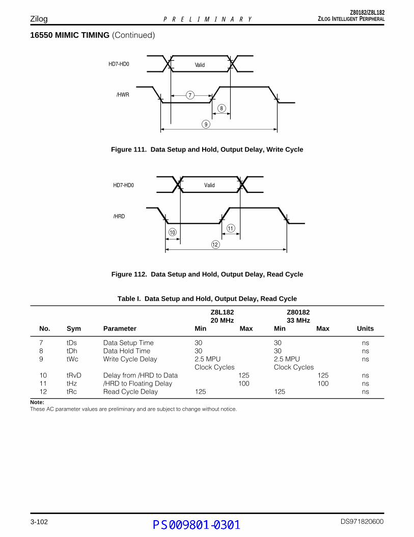
3-102
Z80182/Z8L182ZILOG INTELLIGENT PERIPHERALP R E L I M I N A R YZilog
DS971820600
16550 MIMIC TIMING (Continued)
Figure 111. Data Setup and Hold, Output Delay, Write Cycle
ValidHD7-HD0
/HRD
1011
12
Figure 112. Data Setup and Hold, Output Delay, Read Cycle
Table I. Data Setup and Hold, Output Delay, Read Cycle
Z8L182 Z8018220 MHz 33 MHz
No. Sym Parameter Min Max Min Max Units
7 tDs Data Setup Time 30 30 ns8 tDh Data Hold Time 30 30 ns9 tWc Write Cycle Delay 2.5 MPU 2.5 MPU ns
Clock Cycles Clock Cycles10 tRvD Delay from /HRD to Data 125 125 ns11 tHz /HRD to Floating Delay 100 100 ns12 tRc Read Cycle Delay 125 125 ns
Note:These AC parameter values are preliminary and are subject to change without notice.
ValidHD7-HD0
/HWR
8
9
7
Gayle Gamble
PS009801-0301

3-103
Z80182/Z8L182ZILOG INTELLIGENT PERIPHERALP R E L I M I N A R YZilog
DS971820600
/HRD
/HDDIS
13
Figure 113. Driver Enable Timing
Table J. Driver Enable Timing
Z8L182 Z8018220 MHz 33 MHz
No. Sym Parameter Min Max Min Max Units
13 tRDD /HRD to DriverEnable/Disable 60 60 ns
Note:These AC parameter values are preliminary and are subject to change without notice.
Figure 114. Interrupt Timing RCVR FIFO
14
14
15
15
/WR (MPU)RBR
HINTR(Trigger Level)
HINTR(Line Status RDR
/HRD LSR
/HRD RBR
Gayle Gamble
PS009801-0301

3-104
Z80182/Z8L182ZILOG INTELLIGENT PERIPHERALP R E L I M I N A R YZilog
DS971820600
16550 MIMIC TIMING (Continued)
Table K. Interrupt Timing RCVR FIFO
Z8L182 Z8018220 MHz 33 MHz
No. Sym Parameter Min Max Min Max
14 tSINT Delay from Stop to Set 2 MPU 2 MPUInterrupt Clock Cycles Clock Cycles
15 tRINT Delay from /HRD(RD RBR or RD LSR) 2 MPU 2 MPUto Reset Interrupt Clock Cycles Clock Cycles
Note:These AC parameter values are preliminary and are subject to change without notice.
/RD (MPU)TxFIFO
HINTRTHRE
/WR (Host)THR
/RD (Host)11R
17
16
18
Figure 115. Interrupt Timing Transmitter FIFO
Gayle Gamble
PS009801-0301

3-105
Z80182/Z8L182ZILOG INTELLIGENT PERIPHERALP R E L I M I N A R YZilog
DS971820600
Table L. Interrupt Timing Transmitter FIFO
Z8L182 Z8018220 MHz 33 MHz
No. Sym Parameter Min Max Min Max
16 tHR Delay from /WR 2.5 MPU 2.5 MPU(WR THR) to Reset Clock Cycles Clock CyclesInterrupt
17 TSTI Delay from Stop to 2 MPU 2 MPUInterrupt (THRE) Clock Cycles Clock Cycles
18 TIR Delay from /RD 75 75(RD IIR) to ResetInterrupt (THRIE)
/HRDRD_RBR
/WR (MPU) RCVR FIFO (First Byte that reaches Trigger Level)
/HRXRDY
/HWR (Host)THR
19
14
20
RD (MPU)THR (Last Byte Model)
/HTxRDY21
Note: If FCR0-1TSINT=3 CPUClock Cycles
Figure 116 RCVR FIFO Bytes Other Than First
Gayle Gamble
PS009801-0301

3-106
Z80182/Z8L182ZILOG INTELLIGENT PERIPHERALP R E L I M I N A R YZilog
DS971820600
16550 MIMIC TIMING (Continued)
Table M. RCVR FIFO Bytes Other Than First
Z8L182 Z8018220 MHz 33 MHz
No Sym Parameter Min Max Min Max Units
19 tRXi Delay from /HRD 290 290 nsRBR to /HRxRDY Inactive
20 TWxi Delay from Write to 125 125/HTxRDY Inactive
21 tSXa Delay From Start to 3 MPU 3 MPU/HTxRDY Active Clock Cycles Clock Cycles
Clock Generator
The Z80182/Z8L182 ZIP™ uses the Z182 MPUs on-chipclock generator to supply system clock. The requiredclock is easily generated by connection a crystal to theexternal terminals (XTAL,EXTAL). The clock output runs athalf the crystal frequency for X2 mode.
Recommended characteristics of the crystal and the valuesfor the capacitor are as follows (the values will change withcrystal frequency).
Type of crystal:Fundamental, parallel type crystal(AT cut is recommended).
Frequency tolerance:Application dependent.
CL, Load capacitance:Approximately 22 pF(acceptable range is 20-30 pF).
RS, equivalent-series resistance:≤ 60 OhmsC
IN=C
OUT=15~22 pF.
For PHI > 15 MHz (X2 Mode), it is recommended that anoscillator be used as input to EXTAL.
XTAL
EXTAL
CrystalInputs
C1
C2
Note:These AC parameter values are preliminary and are subject to change without notice.
Figure 117. Circuit Configuration For Crystal
Gayle Gamble
PS009801-0301

3-107
Z80182/Z8L182ZILOG INTELLIGENT PERIPHERALP R E L I M I N A R YZilog
DS971820600
PACKAGE INFORMATION
100-Pin VQFP Package Diagram
Gayle Gamble
PS009801-0301

3-108
Z80182/Z8L182ZILOG INTELLIGENT PERIPHERALP R E L I M I N A R YZilog
DS971820600
PACKAGE INFORMATION (Continued)
100-Pin QFP Package Diagram
Gayle Gamble
PS009801-0301

3-109
Z80182/Z8L182ZILOG INTELLIGENT PERIPHERALP R E L I M I N A R YZilog
DS971820600
ORDERING INFORMATION
Z8L182 Z80182
20 MHz 33 MHzZ8L18220ASC Z8018233ASCZ8L18220FSC Z8018233FSC
For fast results, contact your local Zilog sales office for assistance in ordering the part(s) desired.
Preferred PackageA = VQFP (Very Small QFP)F = Plastic Quad Flatpack
Preferred TemperatureS = 0°C to +70°C
Speeds20 = 20 MHz33 = 33 MHZ
EnvironmentalC = Plastic StandardD = Plastic StressedE = Hermetric Standard
Example:Z 80182 20 F S C is a Z80182, 20 MHz, QFP, 0°C to +70°C, Plastic Standard Flow
Environmental FlowTemperaturePackageSpeedProduct NumberZilog Prefix
Zilog’s products are not authorized for use as critical compo-nents in life support devices or systems unless a specific writtenagreement pertaining to such intended use is executed betweenthe customer and Zilog prior to use. Life support devices orsystems are those which are intended for surgical implantationinto the body, or which sustains life whose failure to perform,when properly used in accordance with instructions for useprovided in the labeling, can be reasonably expected to result insignificant injury to the user.
Zilog, Inc. 210 East Hacienda Ave.Campbell, CA 95008-6600Telephone (408) 370-8000Telex 910-338-7621FAX 408 370-8056Internet: http://www.zilog.com
© 1997 by Zilog, Inc. All rights reserved. No part of this documentmay be copied or reproduced in any form or by any meanswithout the prior written consent of Zilog, Inc. The information inthis document is subject to change without notice. Devices soldby Zilog, Inc. are covered by warranty and patent indemnificationprovisions appearing in Zilog, Inc. Terms and Conditions of Saleonly. Zilog, Inc. makes no warranty, express, statutory, implied orby description, regarding the information set forth herein orregarding the freedom of the described devices from intellectualproperty infringement. Zilog, Inc. makes no warranty of mer-chantability or fitness for any purpose. Zilog, Inc. shall not beresponsible for any errors that may appear in this document.Zilog, Inc. makes no commitment to update or keep current theinformation contained in this document.
Gayle Gamble
PS009801-0301