WTM Microwave Digital
16
ST-48 DESCRIPTION SHORT : 2 DAYS MICROWAVE AND UHF (DIGITAL) CONTENTS 1. Basic Prin ciple of Microwave 2. Need to digital Microwave and advantages of microwave 3. Pulse code modulation. 4. Modulation techniques 5. Radio equipment – Block diagram ex planation (NEC-Make ) 6. Primary and higher order Mux 7 Fading , noise and jitter 8 Space and frequency diversity 9 Microwave Tower 10 Microwave Earthing - importance an d measurement 11 Power sup ply arran gements 12 Periodical arrangements 13 End to end alignment 14 Digital UHF equipment – functioning 15 18 GHZ microwave system used for block working
Transcript of WTM Microwave Digital

8/12/2019 WTM Microwave Digital
http://slidepdf.com/reader/full/wtm-microwave-digital 1/16
ST-48DESCRIPTION
SHORT : 2 DAYS
MICROWAVE AND UHF (DIGITAL)
CONTENTS
1. Basic Principle of Microwave
2. Need to digital Microwave and advantages of microwave
3. Pulse code modulation.
4. Modulation techniques
5. Radio equipment – Block diagram explanation (NEC-Make )
6. Primary and higher order Mux
7 Fading , noise and jitter
8 Space and frequency diversity9 Microwave Tower
10 Microwave Earthing - importance and measurement
11 Power supply arrangements
12 Periodical arrangements
13 End to end alignment
14 Digital UHF equipment – functioning
15 18 GHZ microwave system used for block working

8/12/2019 WTM Microwave Digital
http://slidepdf.com/reader/full/wtm-microwave-digital 2/16
2
1. BASIC PRINCIPLE OF MICROWAVE
Microwave essentially means very short wave . The microwave frequency spectrum is usually taken to extended
form 1 GHZ to 30 GHZ.The main reason why we have to go in for microwave frequency for communication
is that lower frequency band are congested and demand for point to point communication
Continue to increase.
The propagation of the microwave takes place in spacewave in view of the high gain and directivity inthe form of a beam and is similar to that of light .
2. NEED TO DIGITAL MICROWAVE
The modern communication is towards digital transmission to digitize the analog signals PCM techniques are
used . Digital techniques are widely becoming popular for application in switching and multiplexing , thus
necessecitating the use of a new transmission means on radio for the medium and high capacities both for long
haul application and junction working of interexchanges, in urban areas . Thus an extremely rapid transition
from analog to digital radio system at present used in Indian Rly .
ADVANTAGE OF DIGITAL MICROWAVE
Radio links for direct transmission of PCM signals at standard bit rates of 2,8,34 and 140 MB/
Sec.Facilities found by using digital microwave are mentioned below :-
a) Radio repeaters being of re-generative type will give an error free output and there is no accumulation
of noise from hop to hop.
b) Better circuit quality upto threshold,level of the radio receiver .
c) Total system economy is better .
d) Since transmission system is digital , more operational advantages are found , like storage , re-
transmission etc. of information can be easily achived .
e) For data transmission , digital radio is more efficient .
f)
In digital multiplexing , the number of channels loaded does not affect the performance.
3. PULSE CODE MODULATION
Pulse code modulation is adopted for digital multiplexing of channels . In this , each analog signal is converted
into a digital signal such outputs of a number of channels are multiplexed by time division multiplexing to form
a digital base band .
The various stages involved in the pulse code Modulation are :
1) Filtering , 2 ) sampling . 3) Quantising , 4) Encoding , 5) Linecoding
1) FILTERING :-- The incoming analog VF signal frequency is band limited to 0`3 to 3`4 KHZ,by a low
pass filter.
2) SAMPLING :-- The band limited signal is sliced at regular intervals of time to generate pulses of the
continuous analog wave .
The Sampling theorem stipulates a minimum number of samples. The theorem says
that the sampling rate should be equal to or higher than double the highest signal frequency present in the band
limited analog signal .

8/12/2019 WTM Microwave Digital
http://slidepdf.com/reader/full/wtm-microwave-digital 3/16
3
To allow a margin for the fiter, the band limited frequency is taken as 0 – 4KHZ and
the sampling frequency is decided as 8 KHZ .Hence the time period of sampling would be equal to
1/ 8000 Sec =125 us.
3)QUANTISATION:-- The process of sampling generates PAM signals into PCM signal. The discrete
amplitude levels of the samples are first quantified with reference to a standard amplitude scale .This process
is called Quantisation . This gives 28= 256 levels for quantising ( 128 for the positive swing and 128 for the
negative swing). This type of quantisation is called Linear Quantisation.
4) ENCODING:-- Conversion of analog samples into a binary signal is call Encoding. The practicalPCM system use 8 bit code .
5) LINE CODING:-- The binary signal with its DC component is unsuitable for its transmission on
transformer and AC coupled transmission lines.Hence the binary code is modified to suit thecharacteristics of the line. One popular code called HDB3 ( High Density Bipolar 3 ) is employed.
Bit Rate: -- Total No. of bits/ frame= 32x 8 = 256
No. of frame/ Sec =8000
Total no. of bits / Sec= 8000x 256 = 2,048000 bits =2048 K Bit =2.048 M Bits
4. Modulation Technique
Digital information modifies the amplitude , the phase and the frequency of the carrier in discrete steps .
In most of the Digital Radio System , the frequency of the carrier is fixed ;So we need to consider only the phase
and amplitude . The phase and magnitude can be represented in polar or vector co-ordinates as a discrete point
in the socalled I-Q plane .When the carrier phase is shifted between to values to represent binary 0 and 1 it is
called phase shift keying (PSK) .In this system , when four phase states ( 45˚,135˚,225˚,&315˚) are represented ,
it is called Quardrative phase shift keying (QPSK) . The modulation phase state can be generated by addingtogether appropriate amplitudes of in-phase and quadrature carrier . Because by having four discrete states , we
can transmit more information per state in this case .

8/12/2019 WTM Microwave Digital
http://slidepdf.com/reader/full/wtm-microwave-digital 4/16
4
The above figure shows the simplified block diagram of a QPSK(4_PSK) modulator . In QPSK , the incoming
bit-stream is divided into two parallel streams so that each time one bit is fed simultaneously to both I and Q
balanced modulation to construct the 2 bit symbols the carrier output from the modulator is switched under the
control of the digital bit stream and by adding together the I & Q outputs the phase . State diagram is generated .
In this case , the band limiting filter is a bandpass filter at IF .
5. RADIO EQUIPMENT – BLOCK DIAGRAM EXPLANATION
7GHZ DIGITAL MICROWAVE RADIO EQUPT
(NEC-MAKE)
The Radio equipment is compact and fully solid state . Microwave Transmitter receiver employing microwave
Integrated circuits (MIC) for the RF circuit and Field Effect Transistors ( FET) for the low noise microwaveamplifier .
The Digital Transmitter Receiver with switch over units , provide highly efficient transmission services .The
7GHz radio frequencies band (7125 to 7725 MHz) which have a transmission capacity of 340 Mb/s digital
signal alongwith 2Mb/s way side digital signals .
Performance & General Specifications:
1.Operation Frequency Band : 7125 to 7725MHz
2. Repeating Type : Regenerative Repeating
3. Transmission Capacity : 34.368Mb/s x 1stream
(Equivalent 480cl/s)
4.Modulation :4-phase PSK
5.Demodulation :Coherent Detection
6. Service channel :Analogue:3CH
Digital : 4CH

8/12/2019 WTM Microwave Digital
http://slidepdf.com/reader/full/wtm-microwave-digital 5/16
5
7. Type of switch : Relay switching (RF) Hitless switching
8. Wayside Signal : 2.048 Mb/s x 1(optional)
9.Power sourse : 48V DC
10.Power consumption : Approx. 144 W
11.Ambient temperative : 0˚c to + 50˚ c
Transmitter -- Receiver
1 .TX Out –Put Power : +30 dbm (+ 1.0 db to -1.5 db)2. TX frequency stability : Withen +_20 p pm
3. RX Noise figure : Less than 4.0 db
4.RX IF frequency : 70 MHZ
5.RX ACC range : More than 50 db
6.RX Level to the bit error rateof 1x1o : Lower than – 79.5dbm
7.RX Level to the bit error rate of 1x1o : Lower than –83.5dbm
8.TX –RX frequency Difference : 151.614 MHZ
9. Adjacent Channel frequency Difference : 34MHZ
POWER –Supply ( PS) : The PS comprises the DC—DC CONVC.modules.
The DC—DC Conv,produces a regulated +5 v Dc , + 9v Dc , and –10 v Dc from an input power of 48 v Dc.
The regulated +5V DC and –10V DC thus obtained operate modules in the transmitter –Receiver .
When an excessive current flows or an abnormal output voltage goes in to modules , the corresponding power
switch (circuit breaker type) of DC-DC converter trips to interrupt the input power.
Auxiliary Unit (AUX) : The AUX comprises the following two modules. (i) Switch Over SWO) ii) Switch
Over Control (SWO Cont.). The SWO consists of transmitter (Tx) section and receiver (Rx) section.
Tx Section :The HDB-3 signal (34.368Mbps) is applied to attenuator (ATT) and its level to attenuated approx
3dB. Then the signal is delivered to the hybrid and divided into two routes respectively to be supplied to REGand PROT system . The signal is attenuated approx 3dB .
Rx Section : The 34.368Mbs HDB-3 input signal is applied to data switchover circuit , where one of REG and
PROT is selected by the control signal .
When the data switch over operates , the SW OPR indicator lights .The SWO CONT consists of ASc circuit ,
alarm and control circuits .
Tx DPU – The Tx DPU consists of line equalizers, bipolar to unipolar convertor , serial - parallel
convertor,Multiplexer , Scrambler .
34Mb/s unipolar signal is divided into two 17Mb/s unipolar signals in the serial - parallel convertor .
Multiplexer : This circuit multiplexes the digital service channel, way side signal, switch over control , frame
pulse and parity check bits to the corresponding time slot in data signal produced by the buffer memory.
Scambler : This scramble pattern is a 432 bits random pattern produced at the timing pulse generator.
Transmitter —The Tx circuit consists of phase modulator and Transmitter RF circuit .
8/12/2019 WTM Microwave Digital
http://slidepdf.com/reader/full/wtm-microwave-digital 6/16
6
Phase Modulator (PH MOD) : The PH .MOD contains a Tx LOGIC circuit, a Quad MOD circuit and Sc AMP
circuit .
A 70 MHz IF carrier is generated at the 70MHz oscillator and splits into two carrier (LO1,and LO2)for each
0— π modulator . The Phase difference between the two 70 MHz carriers has π/2 radians. In each o— π
modulator , the phase of the 70MHz carrier is modulated to a o—phase or π —phase by input pulse streams. The
output of the two 0- π modulator are then combined for four phase assignment onto a 70 MHz IF carrier. And
the 4 Phase, Phase modulated IF signal thus obtained is amplified by IF amplifier and sent to Tx – RF module atan output level of –3 dBm.
TxRF circuit --- 1 Transmitter Frequency Converter.
2 FET Amplifier (FET AMP ) section
3 Transmitter Local Oscillator (TX LO) section .1. Transmitter Frequency converter : It consists of a mixer and attenuator and a 5 stage band pass
filter. The IF input signal is fed to IF IN terminal and applied to the mixer through an IF attenuator and
also a local frequency signal from trans LO section applied to the mixer. The 5 stage band pass filter passes only the desired frequency signal from trans frequency converter signal
while eliminatingall other frequencies.
2. FET Amplifier (FET AMP) section : It has a three stage FET amplifier sub module with input and output
matching circuit, an isolator an automatic level control circuit and a FET circuit. The first stage of FET
amplifier consists of a 3 -stage FET transistors and a PIN diode attenuator amplifies the RF input signal and
provides a contant output power level at RF OUT. The output power of 3rd stage FET amplifier appears at the
RF OUT terminal through an isolator.
Transmitter Local Oscillator (TX LO) section: It consists of a voltage controlled oscillator (VCO) using
dielectric resonator , voltage control crystal oscillator (VC XO) ,automatic phase control circuit and alarm
circuit (APCand ALM CKT) .
The VCO circuit consists of a transister oscillator (TR) with a varactor diode (X51) to close the feed back loop .
Receiver (RX) : It converts 7GHz band receiving RF signal into a 70 MHz IF signal and amplifiers the 70MHz
IF signal to the required level .
The RX RF consists of 1) Receiver frequency convertor (RX Freq. Conv) section .
2) Receiver Local oscillator .
The RX LO section consists of a voltage controlled oscillator (VCO) using dielectric resonator ,crystal controlled oscillator, automatic phase control circuit and alarm circuit .
Pre-RF Amplifier : The RF input signal is fed to the input terminal RF IN and applied through anisolator to the Pre-RF amplifier. The Pre-RF amplifier is a 2 stage low noise amplifier which is formed
by GaAsFET transistors.Receiver IF circuit (Rx IF) : The convertor 70 MHz IF signal is fed to the Rx IF circuit through a delayequalizer which equalizes on a hop basis , the system delay caused by filtering in the transmitter
receiver and the RF branching circuit .
Demodulator(DEM) : The DEM consists of the 4 phase demodulator (PH DEM ) and the Bitcombiner .The receiver IF signal is applied to the PH DEM and converted to two binary coded pulse
streams. The converted pulse streams from the PH DEM are sent to the Rx DPU through the BIT
COMBINER.
Bit Combiner : It corrects the delay timing of each input data stream in the regular and protection
channel and accomplishes heatless switching by triggering the four switching mode signal so as top
select one of the two data signals.

8/12/2019 WTM Microwave Digital
http://slidepdf.com/reader/full/wtm-microwave-digital 7/16
7
RxDPU Rx DPU consists of demultiplexer , parallel-serial converter , unipolar –bipolar converter .
It functions reversely to the B_ Uconverter operation of transmitting end to feed an original HDB3signal to SWO Module .
6. PRIMARY AND HIGHER ORDER MUX
30 chl. PCM MUX equipment has been designed to convert speech and signaling information at the
transmit end of 30 telephone chl. Of a single digital output bit rate of 2.048 Mb/sec. The relevant
CCITT recommendation are G704 and G744 , which deals with second order PCM Multiplexequipment operating at 8448Mb/s for 120chls . Likewise 34.368MB/s bit stream mux is for 480 chls
and 139.268Mb/s for 1920 chls respectively .
7. FADING , NOISE & JITTER
Fading :- Fading is the term applied to loss of signal received by the radio receiver as its input. This isthe change in path loss between the transmitter at one station and its normal receiver at the following
station. These changes in path loss have to do with atmospheric conditions and the geometry of the path.
Rafio fading is caused by refractive , defractive, reflective effects in connection with the
atmoshphere and fixed objects, which can result in defocusing , blocking and some times cancellation
from multiple paths of varied length, due to the resultant variation in phase angles on arrival at thereceiving antenna.
Types of Fading :- There are normally two types of fading
i) Flat Fading
ii) Selective Fading
Flat Fading: This may be also classified into two types :-

8/12/2019 WTM Microwave Digital
http://slidepdf.com/reader/full/wtm-microwave-digital 8/16
8
i) Ground Reflection Fading:- When radio relay path passes over highly reflective ground or water
.Reflected signal level may be 10dB down (less) than direct path signal if the link crosses areas . Suchas sea , lake , flat & humid area .
ii )Multipath fading :- For a well designed path which is not subjected to diffraction fading or surface
reflection , multipath propagation is the dominant factor in fading below 8GHz .
Selective fading:- Selective fading affects mainly medium capacity (32MB/s , 34MB/s)and highcapacity (98MB/s,140MB/s) digital radio system .
Noise :- Most of the noise and interference produced in the multichannel system are due to main
causes namely thermal noise in an overall contribution of noise from the radio equipment , multiplexequipment and propagation path itself . Thermal and intermodulati on noise is due to random
movement of electron in semiconductors .
Jitter :-Jitter is short term variations of the significant instants of a digital signal from their ideal
position in time . Jitter can be considered as spurious modulation of the digital signal clock . Jitter can
be caused during line transmission of the signal (Line Jitter) or deming channelmultiplexing/demultiplexing jitter .
8. FREQUENCY & SPACE DIVERSITY:
Frequency Diversity:-The refraction of microwave signal is practically independent of frequency .
Signals of quite widely separated frequencies are refracted by some amount under the same
transmisson condition .Greater the separation between the two frequencies less the chance for them tofade simultaneously . The improvement due to frequency diversity is appreciable only when the
difference between the two frequencies is atleast 5% to avoid simultaneous fading on both signals .
For operation of frequency diversity system , two transmitter , one for each frequencies at the
transmitting end and two receivers at the receiving end are required .
Space Diversity :- Fading due to multipath transmission is not always synchronized when signals are
separately received at two points . Space sufficient distance apart vertically spaced antennas are used inmicrowave space diversity system . In a typical space diversity system , the signal from a single
transmitting antenna is received at two antennas having large vertical separtion .
9. Microwave Towers :- The towers are used in microwave system to support antenna or in
some cases , reflectors , design of microwave antenna tower depends upon the following factors :-
a) The number of routes
b)
Space diversity requirementsc) Future expansion (especially VHF/VHF/SPUR)
d) Antenna heights
e) Other loads like lights , transmission line etc. .
All towers fall in two general categories , namely self supporting type and guyed type . Selfsupporting
towers are costly but occupy small areas whereas guyed type though cheaper larger area for the guys .For design of a tower information regarding types and sizes of antennas transmission line , wind
velocity etc. is required to be supplied .

8/12/2019 WTM Microwave Digital
http://slidepdf.com/reader/full/wtm-microwave-digital 9/16
9
10. Microwave Earthing- Importance :-
A good earthing arrangement is required in Microwave station to earth all the equipments and tower .
Lightning protection for microwave instructive is also to be urgently required . for a microwave stationit is considered necessary to keep the earth resistance to a value as low as possible . ( preferably not
more than 2 ohms ) .
The selection of the best type of earth electroad for a given strecture is largely influenced by local soilcharacteristics .In soils of high resistivity and particularly a rock , ring conductors may be a possible solution.
Lightning protection for microwave instructive is also to be a urgently required . For microwavestation it is considered necessary to keep the earth resistance to a value as low as possible.( Preferably
not more than 2ohms.)
The selsction of the best type of earth electrode for a givenstructure is largely influenced by local soil
characteristics .
In soils of high resistivity and particularly a rock , ring conductors may be a possible solution .
Earth Electrodes: There are three main types of earth electrodes:
a) Plate type
b) Rod or pipe type
c) Strip type
Earth measurements conducted by the help of Earth megger .
11. Power Supply arrangement: In Digital Microwave station , power supply is provided
with 48V DC Battery Bank . Two sets of Battery Banks are provided with normal charge dischargecycle is while one set of Battery Bank is load the other set Bank is under charge and vice-versa . The
Battery Banks are charged through 48V DC .
12. Periodical Measurement :- The following measurement are done periodically for Digital
Macrowave equipment .
a) Transmitted output power
b) Transmitted output frequency and Rho frequency
c) AGC characteristics
d) BER Measurement
e) Jitter measurement
a) Transmitted output power:- Measure the transmitter outputpower via directional coupler or
builtin RF Mon on a M.W Power meter with appropriate calibration factor and compare with
standard reading. b) Transmitted output frequency and Rho frequency measure the transmitter`s unmodulated output
frequency after disconnecting based and data on a Frequency counter connected via directional
coupler at RF Mon Test point .Similarly Rho frequency to be checked at the monitoring point provided on the Rho unit .
c) Calibration of AGC level against input receive level . The AGC meter reading of the Receiver
are relative indication of the receiver corner level and can be used to determine the receivedsignal level , under traffic-carrying conditionsAn RF Signal generator is connected to the input
of the receiver to simulate a received signal . The frequency of the generator is set to center

8/12/2019 WTM Microwave Digital
http://slidepdf.com/reader/full/wtm-microwave-digital 10/16
10
frequency of the receiver under test and its level is precisely adjusted to the nominal input
signal level . By varying the generator s̀ output level in steps and noting the AGC readings.AGC calibration curve is drawn .
d) BER Measurement :- BER is the ratio of the number of impaired bits to the actually
transmitted number of bits over a period of time .The Digital Transmission Analyser (DTA) is basically a Pattern Generator and Digital Error
Detector packed into one unit . It is used for the measurement of BER ,Jittre ,etc.
DTA can calculate and display the following parameter :-
1. No. of unavailable seconds(UVS)
2. Unavilable seconds% (UVS)
3. No. of errored seconds% (ES%)4. No. of heavily or seversly errored seconds (SES)
5. Heavily/Severely errored seconds%(SES%)
6. No. of degraded minutes (DM)7. Degraded Minutes% (DM%)
8. No. of seconds with fault Indication .(SFS)
9. Errored seconds % related to 64K Git/s rate (s64%) etc.
e) Jitter Measurements :- Jitter can be caused during line transmissionof the signal (line jitter) or
during channel multiplexing / demultiplexing (Multiplexing jitter) . Jitter is mostly due to un
wanted phase modulation of the digital signal and the jitter can be observed on a Digital storageoscilloscope also.
13. END TO END ALIGNMENT ( DIGITAL MW )
Normal level
2w send -- 0 dBm ] 4w send -- 3.5 dBm] VF level
-
1.0 V + 0.1 V 34.368 MBPs ( Date speed ) + 30dBm -- Assigned RX RF frequency
- 40 dBm -- Assigned RC RF frequency
4w Rec -- 3.5 dBm } V. F. Level 2w Rec -- 7 dBm }

8/12/2019 WTM Microwave Digital
http://slidepdf.com/reader/full/wtm-microwave-digital 11/16
11
14 Digital UHF Equipment
The Nokia DRM 2000 Radio Equjpment operates in the 1.7 -----------2.7 GHz frequency range and
is used to transfer 2 ---------- 16 signal tributaries at 2Mb / s each or 134 Mb/s signal as shown below2 x 2 Mb/s ----------
4 x 2 Mb/s ----------8 x 2 Mb/s --------- 1.7 ------ 2.7 GHz16 x 2 Mb/s---------
OR
1.7---- -----------2.7 GHz
1X34 Mb/s
The main features of NOKIA ̀ sDMR 2ooo are given below ;--
1) nX2 Mb/s (n =2; 4; 8; or 16 capciries with an integrated multipplexer or 1x34MB/S capacity
2) 2Mb/s signal cross-connection facility
3) Dynamic repeater station –Insert /drop/cross-connection facilities for 2Mb/s signals.
4) Wide 1GHz frequency band 1.7------2.7GHz divided into 5 sub-bands complying with relevant CCIR recommendation .5) Adaptive level control with Quality feature (ALCO) ,which provides better performance of the radio network, by
adjusting the transmitted output power according to the information received from the far end.
6) Compatible with Nokia Transmission Management System and hand held Nokia Service terminal7) Five Auxiliary voice and data channels for network management , supervision and telemetry .
8) Systhesiser controlled RF channel selection is made use for easy change of frequencies .
DMR
2000
DMR
2000
8/12/2019 WTM Microwave Digital
http://slidepdf.com/reader/full/wtm-microwave-digital 12/16
12
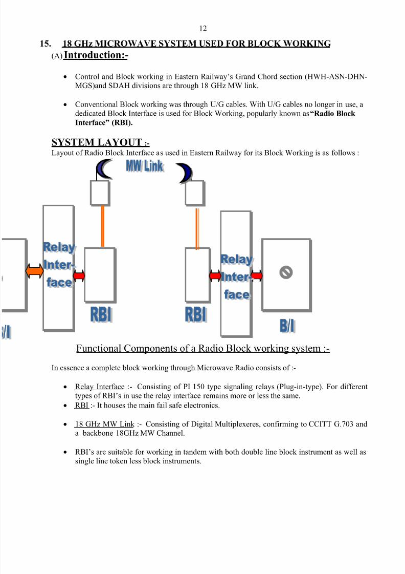
15. 18 GHz MICROWAVE SYSTEM USED FOR BLOCK WORKING
(A) Introduction:-
• Control and Block working in Eastern Railway’s Grand Chord section (HWH-ASN-DHN-MGS)and SDAH divisions are through 18 GHz MW link.
• Conventional Block working was through U/G cables. With U/G cables no longer in use, adedicated Block Interface is used for Block Working, popularly known as “Radio Block
Interface” (RBI).
SYSTEM LAYOUT :-
Layout of Radio Block Interface as used in Eastern Railway for its Block Working is as follows :
Functional Components of a Radio Block working system :-
In essence a complete block working through Microwave Radio consists of :-
• Relay Interface :- Consisting of PI 150 type signaling relays (Plug-in-type). For differenttypes of RBI’s in use the relay interface remains more or less the same.
• RBI :- It houses the main fail safe electronics.
• 18 GHz MW Link :- Consisting of Digital Multiplexeres, confirming to CCITT G.703 anda backbone 18GHz MW Channel.
• RBI’s are suitable for working in tandem with both double line block instrument as well assingle line token less block instruments.

8/12/2019 WTM Microwave Digital
http://slidepdf.com/reader/full/wtm-microwave-digital 13/16
13
Interfacing RBI to 18GHz Link :
RBI’s are connected to the Digital Mux. through a low speed data channel module ( popularly
known as LSDCM). LSDCM provides the necessary clock for the serial communication p[ort of the RBI.
LSDCM card provide 3 different clock speeds, typically 9.6kbps, 4.8 kbps, 2.4 kbps. The output of the LSDCM is hooked to 64kbps time slot of the mux. LSDCM provides synchronous
communication link channel.
DO’S AND DON’TS IN M/W/UHF/VHF STATION
1. Check change over switches , terminals and fuses of the Battery Charger System .
2. Check the Specific gravity of each cell as per specification supplied by the individualfirm . Simultaneously observe the electrolyte level in each cell and maintain the same
between the two engraved marks on the flote .3. Check individual voltage of cells and as a whole the total .4. Daily working of diesel generator should be checked on load for 10min. in each shift .
5. The calibrated switch for the motor reading of R/E parameters should be kept at REC
position .The receive level should be taken note at an half hour interval .
6. The equipment also ,should be cleaned as laid down , time to time .7. Room should be free from dust , Cob webs , as a/c provided , windows and doors
should be kept closed .
8. The earth continuity at the equipment point should be checked ,watered daily evening atearth pit at sun set .
9. R/P circuit to tested at the intervals of 6turns , both signal & speech .
10. The dehydrater pressure should also be checked of an interval at Station .11. Aviation lamp to be switched on just at the advent of evening and to be checked
visually the glow of all the lamps . the should be switched off at own dally .

8/12/2019 WTM Microwave Digital
http://slidepdf.com/reader/full/wtm-microwave-digital 14/16
14

8/12/2019 WTM Microwave Digital
http://slidepdf.com/reader/full/wtm-microwave-digital 15/16
15
BLOCK DIAGRAM OF 7 GHZ DIGITAL RADIO (NEC MAKE)

8/12/2019 WTM Microwave Digital
http://slidepdf.com/reader/full/wtm-microwave-digital 16/16
16


![38998644 Digital Microwave Communication Principles[1]](https://static.fdocuments.net/doc/165x107/5524242a4a7959c8488b45d8/38998644-digital-microwave-communication-principles1.jpg)