Waveguide characterization methodology on lossy silicon substrates
179
POLITECNICO DI TORINO SCUOLA DI DOTTORATO Dottorato in Dispositivi Elettronici – XVII ciclo Tesi di Dottorato Waveguide Characterization Methodology on Lossy Silicon Substrates A theoretical and heuristic study Pablo Silvoni Tutore Coordinatore del corso di dottorato Prof. Giovanni Ghione Prof. Carlo Naldi 14 Febbraio 2005
-
Upload
pablo-federico-gabriel-silvoni -
Category
Documents
-
view
223 -
download
1
description
PhD Thesis by Pablo Silvoni
Transcript of Waveguide characterization methodology on lossy silicon substrates

POLITECNICO DI TORINO
SCUOLA DI DOTTORATODottorato in Dispositivi Elettronici – XVII ciclo
Tesi di Dottorato
Waveguide CharacterizationMethodology on Lossy Silicon
SubstratesA theoretical and heuristic study
Pablo Silvoni
Tutore Coordinatore del corso di dottoratoProf. Giovanni Ghione Prof. Carlo Naldi
14 Febbraio 2005

WAVEGUIDE CHARACTERIZATION METHODOLOGY
ON LOSSY SILICON SUBSTRATES
By
Pablo Silvoni
SUBMITTED IN PARTIAL FULFILLMENT OF THE
REQUIREMENTS FOR THE DEGREE OF
DOCTOR OF PHILOSOPHY
AT
POLITECNICO DI TORINO
TURIN, ITALY
JANUARY 2005
c© Copyright by Pablo Silvoni, 2005

POLITECNICO DI TORINO
DEPARTMENT OF
ELECTRONICS
The undersigned hereby certify that they have read and recommend
to the Faculty of Graduate Studies for acceptance a thesis entitled
“Waveguide Characterization Methodology on Lossy Silicon
Substrates” by Pablo Silvoni in partial fulfillment of the requirements
for the degree of Doctor of Philosophy.
Dated: January 2005
External Examiner:Prof. Marco Pirola
Research Supervisor:Prof. Giovanni Ghione
Examing Committee:Prof. Ermanno Di Zitti
Prof. Heinrich Chirstoph Neitzert
ii

POLITECNICO DI TORINO
Date: January 2005
Author: Pablo Silvoni
Title: Waveguide Characterization Methodology on
Lossy Silicon Substrates
Department: Electronics
Degree: Ph.D. Convocation: 14th February Year: 2005
Permission is herewith granted to Politecnico di Torino to circulate andto have copied for non-commercial purposes, at its discretion, the above titleupon the request of individuals or institutions.
Signature of Author
THE AUTHOR RESERVES OTHER PUBLICATION RIGHTS, ANDNEITHER THE THESIS NOR EXTENSIVE EXTRACTS FROM IT MAYBE PRINTED OR OTHERWISE REPRODUCED WITHOUT THE AUTHOR’SWRITTEN PERMISSION.
THE AUTHOR ATTESTS THAT PERMISSION HAS BEEN OBTAINEDFOR THE USE OF ANY COPYRIGHTED MATERIAL APPEARING IN THISTHESIS (OTHER THAN BRIEF EXCERPTS REQUIRING ONLY PROPERACKNOWLEDGEMENT IN SCHOLARLY WRITING) AND THAT ALL SUCH USEIS CLEARLY ACKNOWLEDGED.
iii

To my Love and Inspiration: my dear wife Adriana and
our three ”Rolling Stones”.
iv
Table of Contents
Table of Contents v
List of Figures viii
Abstract xi
Dedication xii
Acknowledgements xiii
1 Introduction 1
1.1 Motivation . . . . . . . . . . . . . . . . . . . . . . . . . . . . . . . . . 1
1.2 Thesis Overview . . . . . . . . . . . . . . . . . . . . . . . . . . . . . . 2
1.3 Original Contributions . . . . . . . . . . . . . . . . . . . . . . . . . . 3
2 Transmission Line and Waveguide Theory 4
2.1 Introduction . . . . . . . . . . . . . . . . . . . . . . . . . . . . . . . . 4
2.2 TEM mode propagation theory review . . . . . . . . . . . . . . . . . 7
2.2.1 Transmission Line description from Maxwell equations . . . . 10
2.2.2 Telegrapher’s equations and equivalent circuit model . . . . . 19
2.3 Multiconductor transmission line modelling . . . . . . . . . . . . . . . 23
2.4 Multimode description of MTL equations . . . . . . . . . . . . . . . . 31
2.5 Limitations of the quasi-TEM assumptions . . . . . . . . . . . . . . . 40
3 RF Instruments and Tools 46
3.1 Introduction . . . . . . . . . . . . . . . . . . . . . . . . . . . . . . . . 46
3.2 Characterization of linear networks . . . . . . . . . . . . . . . . . . . 47
3.3 Characterization problem in microwaves and millimeter waves . . . . 50
3.4 Scattering parameters theory review . . . . . . . . . . . . . . . . . . . 54
v

3.5 The Vector Network Analyzer . . . . . . . . . . . . . . . . . . . . . . 60
3.5.1 VNA General Description . . . . . . . . . . . . . . . . . . . . 60
3.5.2 Signal Source . . . . . . . . . . . . . . . . . . . . . . . . . . . 61
3.5.3 Test Set . . . . . . . . . . . . . . . . . . . . . . . . . . . . . . 62
3.5.4 Command Unit . . . . . . . . . . . . . . . . . . . . . . . . . . 64
3.6 Systematic error removal and VNA calibration . . . . . . . . . . . . . 66
3.6.1 Measurement Errors . . . . . . . . . . . . . . . . . . . . . . . 67
3.6.2 Twelve Terms Error Model . . . . . . . . . . . . . . . . . . . . 70
3.6.3 Error Box Model (Eight-Term Error Model) . . . . . . . . . . 74
4 Microwave and Millimiter Wave Measurement Techniques 78
4.1 Introduction . . . . . . . . . . . . . . . . . . . . . . . . . . . . . . . . 78
4.2 VNA Calibration process . . . . . . . . . . . . . . . . . . . . . . . . . 78
4.3 Non Redundant Methods . . . . . . . . . . . . . . . . . . . . . . . . . 80
4.3.1 SOLT Calibration Technique . . . . . . . . . . . . . . . . . . . 80
4.3.2 QSOLT Calibration Technique . . . . . . . . . . . . . . . . . . 83
4.4 Self Calibration or Redundant Methods . . . . . . . . . . . . . . . . . 87
4.4.1 TRL technique . . . . . . . . . . . . . . . . . . . . . . . . . . 87
4.4.2 RSOL (UTHRU) technique . . . . . . . . . . . . . . . . . . . 95
5 Calibration & Measurement Tool 98
5.1 Introduction . . . . . . . . . . . . . . . . . . . . . . . . . . . . . . . . 98
5.2 MATLAB Calibration & Measurement Tool . . . . . . . . . . . . . . 99
5.3 Calibration & Measurement program . . . . . . . . . . . . . . . . . . 102
5.3.1 Switch Correction algorithm . . . . . . . . . . . . . . . . . . . 102
5.3.2 TRL algorithm and DUT deembedding . . . . . . . . . . . . . 105
5.3.3 Uploading and calibrated measurements . . . . . . . . . . . . 107
5.4 Coaxial Experimental Results . . . . . . . . . . . . . . . . . . . . . . 111
6 Networks characterization and parameter extraction 116
6.1 Introduction . . . . . . . . . . . . . . . . . . . . . . . . . . . . . . . . 116
6.2 Transmission line characterization methods . . . . . . . . . . . . . . . 118
6.2.1 Circuit parameters extraction from S-Matrix . . . . . . . . . . 123
6.2.2 On Wafer measurements and characterization . . . . . . . . . 126
6.3 MTL characterization methods . . . . . . . . . . . . . . . . . . . . . 134
6.3.1 MTL parameters extraction from S-Matrix . . . . . . . . . . . 142
6.3.2 MTL simulation and experimental results . . . . . . . . . . . . 146
vi

7 Conclusions 151
7.1 Summary . . . . . . . . . . . . . . . . . . . . . . . . . . . . . . . . . 151
7.2 Future works . . . . . . . . . . . . . . . . . . . . . . . . . . . . . . . 153
154
Out of Context... ? 155
A 157
Bibliography 158
vii

List of Figures
2.1 Electromagnetic field structure of a TEM mode of propagation . . . 9
2.2 Two conductor line: (a) Current and Voltage (b) TEM fields . . . . 12
2.3 Derivation contours of the first transmission line equation . . . . . . 13
2.4 Derivation contours of the second transmission line equation . . . . . 14
2.5 Effect of conductor losses, non-TEM field structure . . . . . . . . . . 17
2.6 Transmission Line equivalent lumped circuit model . . . . . . . . . . 20
2.7 Multiconductor Transmission Line system . . . . . . . . . . . . . . . 24
2.8 Modal equivalent circuit of a MTL for two modes of propagation . . . 32
2.9 Conductor equivalent circuit of a MTL for two modes of propagation 38
3.1 Two Port Network Transmission line model . . . . . . . . . . . . . . 48
3.2 Power Waves and Reference Planes interpretation . . . . . . . . . . . 55
3.3 Equivalent circuit of a linear generator . . . . . . . . . . . . . . . . . 57
3.4 HP8510 Block Diagram (Agilent Technologies 2001) . . . . . . . . . . 61
3.5 HP8511 S-Parameter Test Set (Agilent Technologies 2001) . . . . . . 63
3.6 HP8511A Frequency Converter (Agilent Technologies 2001) . . . . . . 64
3.7 HP8510 DSP Block Diagram (Agilent Technologies 2001) . . . . . . . 65
3.8 Twelve Terms Error Model Forward Set . . . . . . . . . . . . . . . . 73
3.9 Twelve Terms Error Model Reverse Set . . . . . . . . . . . . . . . . . 73
3.10 Ideal Free Error VNA and Error Boxes . . . . . . . . . . . . . . . . . 75
3.11 An interpretation of the Error Box Model . . . . . . . . . . . . . . . 76
4.1 1 - Port Error Model (Port 1) . . . . . . . . . . . . . . . . . . . . . . 81
viii

4.2 Ideal VNA and Error Box (Port 1) . . . . . . . . . . . . . . . . . . . 84
4.3 Thru - Line Setup Measurement Reference Planes . . . . . . . . . . . 93
4.4 D.U.T. Setup Measurement Fixture . . . . . . . . . . . . . . . . . . . 94
5.1 R. Marks Error-Box Error Model of a Three-Sampler VNA . . . . . 103
5.2 Measurement System for two 2-Port networks . . . . . . . . . . . . . 104
5.3 Error Model of a Four Sampler VNA . . . . . . . . . . . . . . . . . . 108
5.4 Twelve Terms Error Model - Forward and Backward sets . . . . . . . 109
5.5 S11 Module . . . . . . . . . . . . . . . . . . . . . . . . . . . . . . . . 112
5.6 S11 Phase . . . . . . . . . . . . . . . . . . . . . . . . . . . . . . . . . 112
5.7 S21 Module . . . . . . . . . . . . . . . . . . . . . . . . . . . . . . . . 113
5.8 S21 Phase . . . . . . . . . . . . . . . . . . . . . . . . . . . . . . . . . 113
5.9 LINE Attenuation constant . . . . . . . . . . . . . . . . . . . . . . . 115
5.10 LINE ηeff coefficient . . . . . . . . . . . . . . . . . . . . . . . . . . . 115
6.1 CPW stratified dielectric structure . . . . . . . . . . . . . . . . . . . 129
6.2 per-unit-length Inductance nHy/cm . . . . . . . . . . . . . . . . . . . 130
6.3 per-unit-length Capacitance pF/cm . . . . . . . . . . . . . . . . . . 130
6.4 per-unit-length Resistance Ω/cm . . . . . . . . . . . . . . . . . . . . 131
6.5 per-unit-length Conductance S/cm . . . . . . . . . . . . . . . . . . . 131
6.6 Module of the Characteristic Impedance Zc . . . . . . . . . . . . . . 132
6.7 Phase of the Characteristic Impedance Zc . . . . . . . . . . . . . . . 132
6.8 Attenuation dB/cm . . . . . . . . . . . . . . . . . . . . . . . . . . . 133
6.9 Refraction index ηeff . . . . . . . . . . . . . . . . . . . . . . . . . . 133
6.10 MTL T-circuit model . . . . . . . . . . . . . . . . . . . . . . . . . . . 144
6.11 MTL Π-circuit model . . . . . . . . . . . . . . . . . . . . . . . . . . . 145
6.12 Asymmetric Coupled Microstrip Line . . . . . . . . . . . . . . . . . . 146
6.13 per-unit-length R(f) Ω/cm matrix . . . . . . . . . . . . . . . . . . . . 147
6.14 per-unit-length L(f) nHy/cm matrix . . . . . . . . . . . . . . . . . . 147
6.15 per-unit-length C(f) pF/cm matrix . . . . . . . . . . . . . . . . . . . 148
ix

6.16 Modal attenuation constant dB/cm . . . . . . . . . . . . . . . . . . . 149
6.17 Modal Refractive index dB/cm . . . . . . . . . . . . . . . . . . . . . . 149
6.18 Modal Cross Power ζnm merit coefficient index . . . . . . . . . . . . . 150
x

Abstract
PABLO F. G. SILVONI. Waveguide Characterization Methodology on Lossy Silicon
Substrates. Advisor: Prof. Dr. Giovanni Ghione.
A theoretical review of transmission line and waveguide theory was given. Valid-
ity and limitations were stated and discussed. An overview of the state of the art of
the experimental characterization for linear networks, microwave and millimeter mea-
surement instruments, tools and error models were described and discussed. Vector
network analyzer calibration techniques were presented and discussed. A calibration
and measurement tool was developed based on the TRL calibration technique. Ex-
perimental results based on TRL and SOLT calibration techniques were made and
compared on coaxial media. Single transmission line characterization methods were
discussed and compared. A characterization method based on scattering parame-
ters was implemented and experimental and simulated results were compared and
discussed. Multi-transmission line characterization methods were discussed and com-
pared. A multi-transmission line characterization method, based on the scattering
matrix without optimization was implemented. Experimental results were compared
with an experiment selected in the scientific literature.
xi

Dedication
This thesis is dedicated to Dr. Daniel Avalos, Full Professor of Physics of the Facultad
de Ingeniera de la Universidad Nacional de Mar del Plata, Argentina; who shared with
us his love for experiments and the pleasure for the interpretation of reality considering
Physics a great adventure of the thought. His passion, fantasy and creativity to explain
the phenomena, his faith in his students and his sense of humor, were the force and
motivation for a lot of his students, friends and children; reminding us the fact that
Imagination is more important than knowledge as uncle Albert taught us almost like
a belief.
My recognition forever.
xii

Acknowledgements
I’d like to express my sincere gratitude to Prof. Giovanni Ghione, my thesis advisor,
for his support and guidance, help and continuous encouragement during my graduate
studies and research work.
I’d also like to express my sincere appreciation and gratitude to Prof. Marco
Pirola for the constant intellectual help and patience along the research work. This
thesis would not have been possible without his continuous help.
I like to thank to Prof. Dr. Gianpaolo Bava for all his encouragement, intellectual
help, fine sense of humor and patience in our discussions. I would like to thank the
whole Gruppo di Microonde Politecnico di Torino for all its great cooperation and
participation, especially to Dr. Michelle Goano, Dr. Franco Fiori, Dr. Valeria
Teppatti, Prof. Andrea Ferrero, Prof. Pisani and Mr. Renzo Maccelloni.
I’d like to thank to my great friend Carlos Issazadeh and his family who always
believed, and helped me in the moments when I forgot to believe in myself.
I’d like to thank to my good friends Jorge Finocchietto for all his faith and love,
who constantly supported me; and Stefan Tannenbaum who helped, supported and
encouraged me with patience all the time.
I’d like to thank to my cousin Marcelo, Patricio Valdivia and his wife Marytas,
Martin Fernandez and his wife Silvia, Roberto Kiessling and Pedro Kolodka for their
love, faith and sincere friendship; and to all my friends for their love and support.
I’d like to thank to nonno Giovanni, for all his love.
I’d like to thank to my aunt and godmother Mirta for all his all his love.
I’d like to thank to my mother and father, my brother Ricardo and my sisters
Maria Gabriella, Annamaria and Luisa, my uncle Mirta and all my family who have
always stood by me and made it possible for me to pursue graduate studies and for
giving love, spiritual and material support to my wife and children all this time.
xiii

xiv
Most of all I’d like to thank to my lovely and dear wife Adriana, my son Juan
Salvador, and my daughters Constanza Guadalupe and Maria Jose who have always
supported me with love, faith and patient. They are my source of inspiration and
motivation.
I like to thank the Lord for all his Blessings.
To all of you, many thanks
Turin, Italy Pablo Silvoni
Febbruary 1st, 2005

Chapter 1
Introduction
1.1 Motivation
Active research in silicon technology has become more specialized in subfields related
to RF and high-speed applications derived from the complexity and sophistication of
embedded systems and integrated circuits, paradigms for the present state of the art
of the information technology.
In the last decade, the global expansion of mobile telecommunications and high-
speed electronic applications has stimulated both, basic and applied research on the
main issues critical to the implementation of these sophisticated devices.
In particular such embedded systems, containing complex functions, are integrated
and interconnected within complex communication structures; and the high circuit
density together with the ever increasing operating frequency requires to deal with
the problem of Electro Magnetic Interference.
EMI phenomena need to be taken into account for design, requiring the devel-
opment of more accurate models of devices and inter-chip interconnections because
1

2
interconnection of high-speed systems has become a critical issue since they are af-
fected by EMI phenomena as crosstalk, time delay and distortion [2][21].
The performance of system and on-chip interconnections has become crucial for
high-speed and high frequency applications [12] and CAD tools need to use accurate
models based on EM propagation theory, which must be accurately developed and
validated.
From these considerations comes the motivation for the present work, conceived as
a framework of ideas integrated into a methodology for characterizing high frequency
waveguides on silicon substrates.
This methodology was intended to be based both on a theoretical and experimental
study which can be extended to waveguides on different substrate materials.
1.2 Thesis Overview
The present work is the result of an applied research program which seeks primarily
for a fundamental understanding of the phenomena under investigation and at the
same time looks for possible applications [44].
The present work was divided to seven chapters, being the present the first chapter.
Chapter 2 is a review of the transmission lines theory, its validity, assumptions
and limitations.
Chapter 3 is an overview of the state of the art of the experimental characterization
for linear networks, it describes the vector network analyzer VNA and presents an
introduction to the microwave and millimeter measurement problem together with a
description of the error models.
Chapter 4 presents the more modern microwave and millimeter measurement and

3
calibration techniques, giving an extensive description of the TRL technique which is
extensively used for planar waveguide characterizations.
Chapter 5 describes a calibration and measurement tool specially developed for
the present work. Experimental results are given and discussed.
Chapter 6 presents single and multi-transmission line characterization methods
based on experimental measurements of scattering parameters. Experimental results
and simulations comparison are given and discussed.
Chapter 7 contains the Conclusions.
An Appendix contains a User’s Guide of the calibration and measurement tool
developed ad hoc for the present work.
1.3 Original Contributions
A Calibration and Measurement tool was developed in MATLAB environment based
on the TRL algorithm. This tool uses the capacity of the VNA HP8510C to be
connected to a remote computer through an IEEE 488.2 interface. Different features
and experimental results are described in Chapter 5.
Chapter 2
Transmission Line and WaveguideTheory
2.1 Introduction
In this chapter, a review of the relevant theoretical topics of linear transmission lines
and multiconductor transmission line (MTL) models will be presented with a rigorous
physics description using Maxwell equations. Then, the Telegrapher’s equation will be
developed as a distributed-parameter, lumped-circuit description that is the common
model used in engineering. Limitations of the descriptions will be presented and
discussed.
Transmission line structures serve to guide electromagnetic (EM) waves between
two points. The analysis of transmission lines consisting of two parallel conductors of
uniform cross section is a fundamental and well understood subject in electrical engi-
neering. However, the analysis of similar lines consisting of more than two conductors
is somewhat more difficult than the analysis of two-conductor lines. Matrix methods
and notation provide a straightforward extension of most of aspects of two-conductor
to multiconductor transmission lines.
4

5
First, the key assumptions of these theoretical descriptions will be aimed at under-
standing their restrictions on the applicability of the representations and the validity
of the results obtained.
Electromagnetic fields are, actually, distributed continuously throughout space.
If a structure’s largest dimension is electrically small, i.e., much less than a wave-
length, we can approximately lump the EM effects into circuit elements as in lumped-
circuit theory and define alternative variables of interest such as voltages and cur-
rents. The transmission-line formulation views the line as a distributed-parameter
structure along the propagation axis and thereby extends the lumped-circuit analysis
techniques to structures that are electrically large in this dimension. However, the
cross-sectional dimensions, e.g., conductor separations, must be electrically small in
order for the analysis to yield valid results.
The fundamental assumption for all transmission-line formulations and analysis,
whether for a two-conductor or a MTL, is that the field structure surrounding the
conductors obeys to a Transverse Electro Magnetic or TEM structure. A TEM field
structure is one in which the electric and magnetic fields in the space surrounding the
line conductors are transverse or perpendicular to the line axis which will be chosen
to be the z axis of a rectangular coordinate system. The waves on such lines are said
to propagate in the TEM mode.
Transmission-line structures having electrically large cross-sectional dimensions
have, in addition to the TEM mode of propagation, other higher-order modes of
propagation. An analysis of these structures using the transmission line equation
formulation would then only predicts the TEM mode component and does not rep-
resent a complete analysis. Other aspects, such as imperfect line conductors, also

6
may invalidate the TEM mode transmission-line equation description. In addition,
an assumption inherent in the MTL equation formulation is that the sum of the line
currents at any cross section of the line is zero; and it is assumed that a conductor,
the reference conductor, is the return for all the line currents. This last assumption
may not be true and there may be other non-TEM currents in existence on the line
conductors due to EMI and/or asymmetries in physical terminal excitation.
A complete solution of the transmission-line and MTL structures, which does
not presuppose only the TEM mode, can be obtained with Full-Wave solutions of
Maxwell’s equations, techniques that require numerical methods and are outside of
the scope of this work.
In my approach only the analytical solutions for TEM and quasi-TEM modes of
propagation that are consistent with the characterization parameters which can ex-
perimentally be measured as the scattering matrix, and all other two-port descriptions
defined for TEM structures, will be considered.

7
2.2 TEM mode propagation theory review
First to examine the classical formulae and parameters of Transmission Line and
waveguide theory, the results of the TEM propagation mode will be reviewed.
The fundamental assumption in any transmission line formulation is that the
electric field intensity vector−→E (x, y, z, t) and the magnetic field intensity vector
−→H (x, y, z, t) satisfy the transverse electromagnetic (TEM) field structure, and they
lie in a plane (the x-y plane) transverse or perpendicular to the line axis (the z axis).
Considering a rectangular coordinate system as shown in Fig. 2.1 where a propa-
gating TEM wave in which field vectors are assumed to lie in a plane transversal
to the propagation direction is illustrated, we denote the field vectors with a t sub-
script to denote transverse. It is assumed that the medium is homogeneous, linear
and isotropic and characterized by the scalar parameters of electric permitivity ε,
magnetic permeability µ and conductivity σ. Then Maxwell’s equations become:
∇×−→E t = µ∂−→H t
∂t(2.2.1)
∇×−→H t = σ−→E t − ε
∂−→H t
∂t(2.2.2)
The ∇ operator can be broken into two components, one component, ∇z, in the
z direction and one component, ∇t, in the transverse plane as ∇ = ∇t +∇z, where:
∇t = x · ∂
∂x+ y · ∂
∂y
∇z = z · ∂
∂z

8
being x, y and z the unit vectors in the rectangular directions. Separating (2.2.1)
and (2.2.2) by equating the field components in the z direction and in the transverse
plane gives:
z × ∂−→E t
∂z= −µ
∂−→H t
∂t(2.2.3)
z × ∂−→H t
∂z= σ
−→E t − ε
∂−→H t
∂t(2.2.4)
∇t ×−→E t = 0
∇z ×−→H t = 0(2.2.5)
Equations (2.2.5) are identical to those for static fields. As a consequence, the
electric and magnetic fields of a TEM field distribution satisfy a static distribution
in the transverse plane. Then, each of the transverse field vectors can be defined as
the gradients of some auxiliary scalar fields or potential functions Φ and Ψ, such as:
−→E t = g(z, t) · ∇Φ(x, y)−→H t = f(z, t) · ∇Ψ(x, y)
(2.2.6)
And by applying Gauss’s laws:
∇t · −→E t = 0 ∇2t Φ(x, y) = 0
∇t · −→H t = 0 ∇2t Ψ(x, y) = 0
(2.2.7)
Equations (2.2.7) show that these scalar potential functions satisfy Laplace’s equa-
tion in any transverse plane as they do for static fields. This permits the unique

9
Figure 2.1: Electromagnetic field structure of a TEM mode of propagation
definition of voltage between two points in a transverse plane as the line integral of
the transverse electric field between those two points:
V (z, t) = −∫ 2
1
−→E t · d~l (2.2.8)
Similarly the last equation of (2.2.7) shows that we may uniquely define current in
the z direction as the line integral of the transverse magnetic field around any closed
contour lying solely in the transverse plane:
I(z, t) = −∮
ct
−→H t · d~l (2.2.9)
These results can be applied to a TEM field structure propagating along a uni-
form transmission line with two parallel conductors to obtain the transmission line
equations as shown in the following section.
10
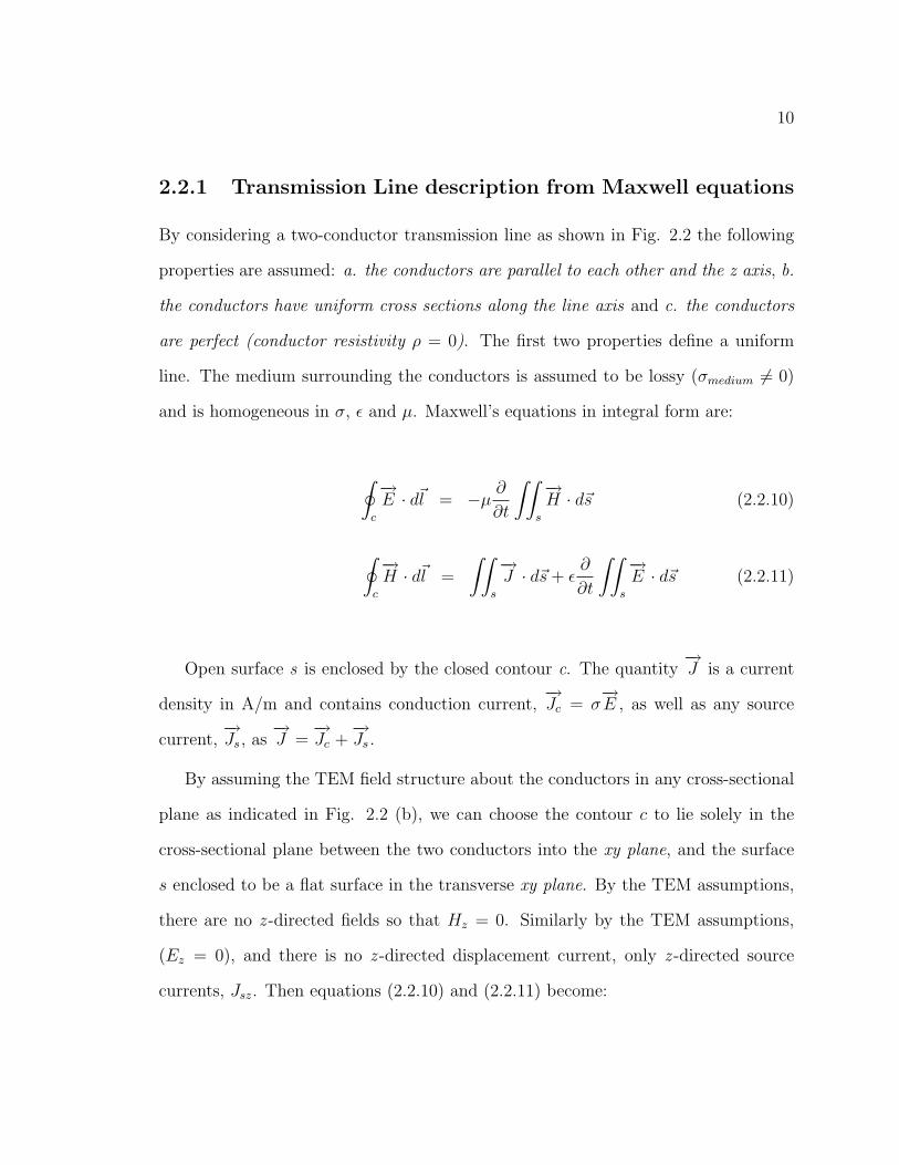
2.2.1 Transmission Line description from Maxwell equations
By considering a two-conductor transmission line as shown in Fig. 2.2 the following
properties are assumed: a. the conductors are parallel to each other and the z axis, b.
the conductors have uniform cross sections along the line axis and c. the conductors
are perfect (conductor resistivity ρ = 0). The first two properties define a uniform
line. The medium surrounding the conductors is assumed to be lossy (σmedium 6= 0)
and is homogeneous in σ, ε and µ. Maxwell’s equations in integral form are:
∮
c
−→E · d~l = −µ
∂
∂t
∫∫
s
−→H · d~s (2.2.10)
∮
c
−→H · d~l =
∫∫
s
−→J · d~s + ε
∂
∂t
∫∫
s
−→E · d~s (2.2.11)
Open surface s is enclosed by the closed contour c. The quantity−→J is a current
density in A/m and contains conduction current,−→Jc = σ
−→E , as well as any source
current,−→Js , as
−→J =
−→Jc +
−→Js .
By assuming the TEM field structure about the conductors in any cross-sectional
plane as indicated in Fig. 2.2 (b), we can choose the contour c to lie solely in the
cross-sectional plane between the two conductors into the xy plane, and the surface
s enclosed to be a flat surface in the transverse xy plane. By the TEM assumptions,
there are no z -directed fields so that Hz = 0. Similarly by the TEM assumptions,
(Ez = 0), and there is no z -directed displacement current, only z -directed source
currents, Jsz. Then equations (2.2.10) and (2.2.11) become:

11
∮
c
(Exdx + Eydy) = −µ∂
∂t
∫∫
s
Hzdxdy = 0 (2.2.12)
∮
c
(Hxdx + Hydy) =
∫∫
s
Jzdxdy + ε∂
∂t
∫∫
s
Ezdxdy (2.2.13)
=
∫∫
s
Jszdxdy
Equations (2.2.12) and (2.2.13) are identical to those for static time variation as
was pointed in equation (2.2.7) in the TEM assumptions. Therefore, from equation
(2.2.12) it may be uniquely defined the voltage between the two conductors, indepen-
dent of path, so long as we take the path to lie in a transverse plane as indicated in
Fig. 2.2 (b), in the same way as was pointed in equation (2.2.8) as:
V (z, t) = −∫ 1
0
−→E t · d~l (2.2.14)
Similarly, equation (2.2.13) allows the unique definition of the current by choosing
a closed contour in the transverse plane encircling one of the conductors as indicated
in Fig. 2.3, in the same way as was pointed in equation (2.2.9) as:
I(z, t) = −∮
ct
−→H t · d~l (2.2.15)
This current defined by (2.2.15) lies solely on the surface of the perfect conductor.
If both conductors are enclosed with the same contour it can be shown that the net

12
Figure 2.2: Two conductor line: (a) Current and Voltage (b) TEM fields
current is zero, being the current in any cross section on the lower conductor equal
and opposite to the current on the upper conductor.
Now the transmission-line equations can be derived in terms of the voltage and
current defined above. First, the open surface s is considered , enclosed by the contour
cl as is shown in Fig. 2.3. Integrating Faraday’s Law given in equation (2.2.10) around
this contour gives:
∫ 2
1
−→Ez · d~l +
∫ 3
2
−→Et · d~l +
∫ 4
3
−→Ez · d~l +
∫ 1
4
−→Et · d~l = −µ
∂
∂t
∫∫
s
−→Ht · d~s (2.2.16)
By defining the voltages between the two conductors as in (2.2.14) with the TEM

13
Figure 2.3: Derivation contours of the first transmission line equation
assumption of Ez = 0 gives:
V (z + ∆z, t) = −∫ 3
2
−→Et(x, y, z + ∆z, t) · d~l
V (z, t) = −∫ 1
4
−→Et(x, y, z, t) · d~l
Therefore (2.2.16) becomes:
V (z + ∆z, t)− V (z, t) = −µ∂
∂t
∫∫
s
−→Ht · d~s
Rewriting this and taking the limit as ∆z → 0 gives:
∂
∂zV (z, t) = −µ
∂
∂tlim
∆z→0
1
∆z
∫∫
s
−→Ht · d~s (2.2.17)
14
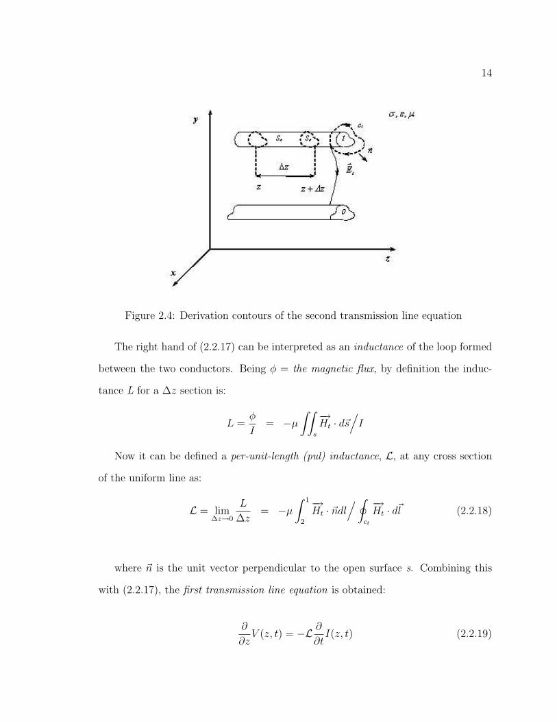
Figure 2.4: Derivation contours of the second transmission line equation
The right hand of (2.2.17) can be interpreted as an inductance of the loop formed
between the two conductors. Being φ = the magnetic flux, by definition the induc-
tance L for a ∆z section is:
L =φ
I= −µ
∫∫
s
−→Ht · d~s
/I
Now it can be defined a per-unit-length (pul) inductance, L, at any cross section
of the uniform line as:
L = lim∆z→0
L
∆z= −µ
∫ 1
2
−→Ht · ~ndl
/ ∮
ct
−→Ht · d~l (2.2.18)
where ~n is the unit vector perpendicular to the open surface s. Combining this
with (2.2.17), the first transmission line equation is obtained:
∂
∂zV (z, t) = −L ∂
∂tI(z, t) (2.2.19)

15
To derive the second transmission line equation, we recall the continuity equation
which states that the net outflow of current from a closed surface Sv equals the time
rate of decrease of the charge enclosed Qenc by that surface:
∫∫
Sv
−→J · d~s = − ∂
∂tQenc (2.2.20)
Integrating the continuity equation over the closed surface Sv of length ∆z that
encloses each conductor as is shown in Fig. 2.4 gives:
∫∫
So
−→J · d~s +
∫∫
Se
−→J · d~s = − ∂
∂tQenc (2.2.21)
The terms in last equation become:
∫∫
Se
−→J · d~s = I(z + ∆z, t)− I(z, t); (2.2.22)
∫∫
So
−→J · d~s = σ
∫∫
So
−→Et · d~s (2.2.23)
The right-hand side of (2.2.21) can be defined in terms of a per-unit-length capac-
itance C. From Gauss’ law, the total charge enclosed by a closed surface Sv is:
Qenc =
∫∫
Sv
−→E · d~s (2.2.24)

16
The capacitance between two conductors for a ∆z section is:
C =Qenc
V
then, by substituting (2.2.24) and observing Fig. 2.4, the per-unit-length capaci-
tance C is defined as:
C = lim∆z→0
C
∆z= −
∮
ct
−→Et · ~nd~l
/ ∫ 1
0
−→Et · d~l (2.2.25)
Similarly, the conductance between the two conductors for a ∆z section can be
defined as:
G =
∫∫
So
−→J · d~s
/V (z, t) (2.2.26)
Then, from (2.2.23) we can define per-unit-length conductance G as:
G = lim∆z→0
G
∆z= −σ
∮
ct
−→Et · ~nd~l
/∫ 1
0
−→Et · d~l (2.2.27)
Finally, substituting (2.2.22), (2.2.25) and (2.2.27) into (2.2.21) gives the second
transmission-line equation:
∂
∂zI(z, t) = −GV (z, t)− C ∂
∂tV (z, t) (2.2.28)
Equations (2.2.19) and (2.2.28) are the transmission-line equations represented as
a coupled set of first-order, partial differential equations in the line voltage, V (z, t),
and line current I(z, t).

17
Figure 2.5: Effect of conductor losses, non-TEM field structure
Most of the previous derivations assumed perfect conductors. Unlike losses in the
surrounding medium, lossy conductors invalidate the TEM field structure assumption.
As is shown in Fig. 2.5, the line current flowing through the imperfect line conductor
generates a nonzero electric field along the conductor surface, Ez(z, t), which is di-
rected in the z direction violating the basic assumption of the TEM field structure in
the surrounding medium. The total electric field is the sum of the transverse compo-
nent Et(z, t) and this z directed component Ez(z, t). However, if the conductor losses
are small, this resulting field structure is almost TEM. This is the quasi-TEM as-
sumption and, although the transmission line equations are no longer valid, they are
nevertheless assumed to represent the situation for small losses through the inclusion
of the per-unit-resistance parameter R.
Another limitation of the transmission-line equations description is that non ho-
mogeneous surrounding medium invalidates the basic assumption of a TEM field

18
structure because different portions of this medium are characterized by different di-
electric constants εi and magnetic permeabilities µi. Then, the phase velocities vphi
(vphi= 1/
√εiµi) of TEM waves in these regions will be different; when it is required
for a TEM field structure to have only one propagation velocity in the medium. Nev-
ertheless, the transmission-line equations are solved by assuming to represent the
situation so long as these velocities are not substantially different, referred to as the
quasi-TEM assumption. To describe this situation of a non homogeneous medium, an
effective dielectric constant εeff is defined so that if the transmission line conductors
are immersed in a homogeneous dielectric having this εeff , the propagation velocities
and all other attributes of the solutions for the original non homogeneous medium
and for this one will be the same.
In order to solve the transmission-line equations by obtaining a closed analytical
solution for them, the above quasi-TEM assumptions will be taken into account by
adding the conductor losses to the model in a heuristic or engineering approach.
This is the classical form of Telegrapher’s equations with all the above described
parameters involved in a distributed-parameter, lumped circuit as will be seen in the
next paragraphs.

19
2.2.2 Telegrapher’s equations and equivalent circuit model
The previous two derivations of the transmission-line equations were rigorous. In
order to add the conductor losses to the transmission-line model, a quasi-TEM field
structure will be assumed, and the usual derivation of a distributed-parameter, lumped
equivalent circuit model will be developed. The concept stems from the fact that
lumped-circuit concepts are only valid for structures whose largest dimension is elec-
trically small, i.e., much less than a wavelength, at the frequency excitation.
If a structural dimension is electrically large, we may break the transmission line
into the union of electrically small substructures and can then represent each sub-
structure with a lumped circuit model. In order to apply this to a transmission-line,
an equivalent lumped circuit model is considered in Fig. 2.6. In this figure, the
transmission line is subdivided into infinitesimal pieces of incremental lumped cir-
cuits composed by the per-unit-length (pul) parameters R, L, G and C, embedded
and connected within little cross sections of ∆z length. In the approach, these R, L,
G and C pul parameters will be assumed to be constant with frequency to obtain the
solution of Telegrapher’s equations. This assumption will be reexamined later when
the propagation of EM waves with microwave and millimeter wavelengths into silicon
waveguides (microstrip lines, CPWs, etc) will be considered.
From Fig. 2.6 it is straightforward to derive the circuital equations that describe
the lumped circuit model [41] known as the Telegrapher’s equations :
∂
∂zV (z, t) = −RI(z, t)− L ∂
∂tI(z, t) (2.2.29)
∂
∂zI(z, t) = −GV (z, t)− C ∂
∂tV (z, t) (2.2.30)
20
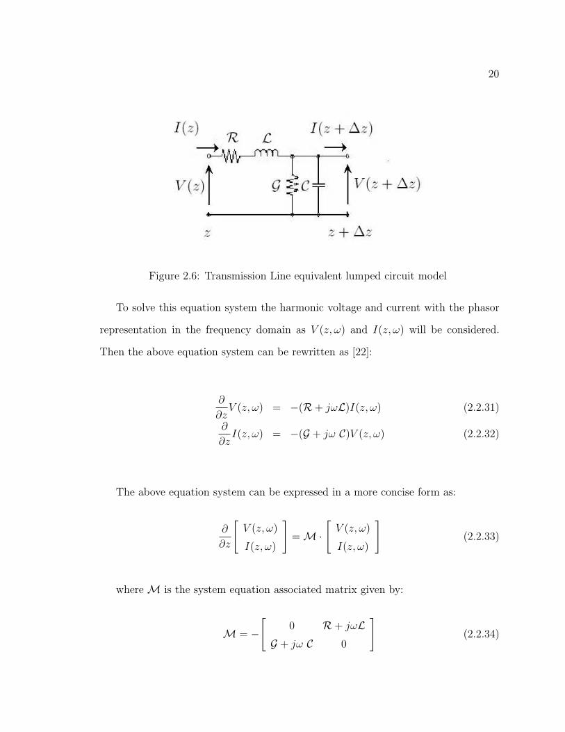
Figure 2.6: Transmission Line equivalent lumped circuit model
To solve this equation system the harmonic voltage and current with the phasor
representation in the frequency domain as V (z, ω) and I(z, ω) will be considered.
Then the above equation system can be rewritten as [22]:
∂
∂zV (z, ω) = −(R+ jωL)I(z, ω) (2.2.31)
∂
∂zI(z, ω) = −(G + jω C)V (z, ω) (2.2.32)
The above equation system can be expressed in a more concise form as:
∂
∂z
[V (z, ω)
I(z, ω)
]= M ·
[V (z, ω)
I(z, ω)
](2.2.33)
where M is the system equation associated matrix given by:
M = −[
0 R+ jωLG + jω C 0
](2.2.34)

21
The solution of the Telegrapher’s equations, expressed as in (2.2.33) is given by:
[V (z, ω)
I(z, ω)
]= Ev · exp(Λ.z) ·
[V +
0
V −0
](2.2.35)
Constants V +0 and V −
0 are determined by the environment conditions. Ev is the
eigenvector matrix and Λ is the eigenvalue matrix of the system given by:
Ev =
[1 1
Yc −Yc
], and Λ =
[−γ 0
0 γ
](2.2.36)
The variable γ is the propagation constant and Zc = Y −1c is the characteristic
impedance of the system expressed as functions of the pul parameters R, L, G and Cand given by:
γ =√
(R+ jωL) · (G + jω C) (2.2.37)
Zc =
√(R+ jωL)
(G + jω C)(2.2.38)
These are the fundamental parameters that describe the behavior of the trans-
mission line. The propagation constant γ can be expressed as a complex number as
follows:
γ = α + jβ (2.2.39)

22
where α represents the attenuation constant that takes into account the power
attenuation of the EM wave along the line, and β is the phase constant that represents
the behavior of the phase velocity vph = ω/β of the EM wave along the line.
Then, modal voltage V (z, ω) and modal current I(z, ω) along the line can be
expressed as the well known expressions based on the travelling waves or forward
intensities V +, I+ and the backward intensities V −, I− as:
V (z, ω) = V +0 · e−γ.z + V −
0 · eγ.z = V +(z) + V −(z) (2.2.40)
I(z, ω) =V +
0
Zc
· e−γ.z − V −0
Zc
· eγ.z = I+(z) + I−(z) (2.2.41)
From the above considerations it is clear that the pul parameters R, L, G and
C fully characterize a transmission line, and they are analytically related with the
EM wave parameters γ = α + jβ and Zc. As will be shown in next chapters these
parameters can be obtained indirectly through two-ports scattering parameters mea-
surements and using matrix calculations.
In next paragraphs an extension of this theory will be applied to a multiconductor
transmission line system and matrix equations will be obtained and solved in analogy
with the Telegrapher’s equations.

23
2.3 Multiconductor transmission line modelling
The results obtained in the previous chapter for the general properties of a two con-
ductors transmission line will be extended to multiconductor transmission lines or
MTLs. As seen, the TEM field structure and associated mode of propagation is
the fundamental, underlying assumption in the representation of a transmission-line
structure with the transmission-line equations. The class of lines will be restricted
to those that are uniform lines consisting of (n + 1) conductors of uniform cross sec-
tion that are parallel to each other. The same quasi TEM assumptions used for the
two conductors transmission line will be used to derive the MTLs equations from
an equivalent circuit that takes into account lossy conductors and inhomogeneous
surrounding medium. The MTL equations will have an identical form to the Teleg-
rapher’s equations by using a matrix notation.
A full development of the MTL equations will be not given, but only the useful
results related to the experimental characterization will be shown. For developments
are refer to works of K. D. Marx [39], C. Paul [41] and Marks and Williams [8].
Taking into account Fig. 2.7, a set of n conductors (1,2,..i,..,j...n) and a reference
conductor 0 define a multiconductor transmission line system. Maxwell equations
applied to these systems demonstrate that different i modes propagate along the z
axis, but their modal parameters, the modal propagation constant γmiand modal
characteristic impedance Zmi, can not be measured directly. The more common
description of the system starts by applying Kirchoff’s laws to the different ith circuits
given by the ith conductors and the reference conductor. It is assumed that the
reference conductor collects all the n conductor currents and applying the 2nd Kirchoff
law gives I0 =∑n
k=1 Ik.

24
Figure 2.7: Multiconductor Transmission Line system
This model represents very well the cases of coupled microstriplines, coupled
CPW transmission lines, and PCB traces on different substrates and will be assumed
throughout this work.
In order to apply the circuit theory to the model shown in Fig. 2.7, the different pul
matrices parameters R, L, C and G,that describe the mutual interactions between
the different conductors, will be defined. From the model in Fig. 2.7 the voltage V
and current I vectors are defined as:
V(z, t) =
V1(z, t)...
Vi(z, t)...
Vn(z, t)
I(z, t) =
I1(z, t)...
Ii(z, t)...
In(z, t)
(2.3.1)
25
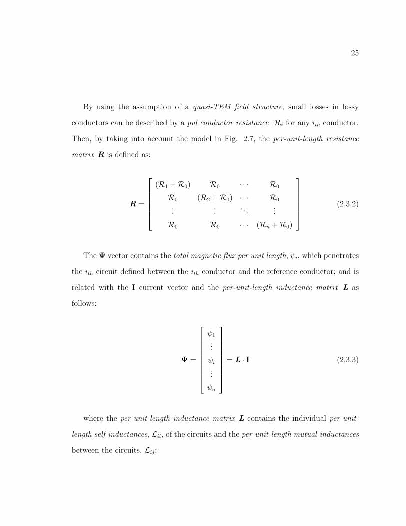
By using the assumption of a quasi-TEM field structure, small losses in lossy
conductors can be described by a pul conductor resistance Ri for any ith conductor.
Then, by taking into account the model in Fig. 2.7, the per-unit-length resistance
matrix R is defined as:
R =
(R1 +R0) R0 · · · R0
R0 (R2 +R0) · · · R0
......
. . ....
R0 R0 · · · (Rn +R0)
(2.3.2)
The Ψ vector contains the total magnetic flux per unit length, ψi, which penetrates
the ith circuit defined between the ith conductor and the reference conductor; and is
related with the I current vector and the per-unit-length inductance matrix L as
follows:
Ψ =
ψ1
...
ψi
...
ψn
= L · I (2.3.3)
where the per-unit-length inductance matrix L contains the individual per-unit-
length self-inductances, Lii, of the circuits and the per-unit-length mutual-inductances
between the circuits, Lij:

26
L =
L11 L12 · · · L1n
L21 L22 · · · L2n
......
. . ....
Ln1 Ln2 · · · Lnn
(2.3.4)
With similar considerations to the two conductors transmission line, the transverse
conduction current flowing between conductors can be considered by defining per-
unit-length conductances, Gij, between each pair of conductors. Then a per-unit-length
conductance matrix, G, that represents the conduction current flowing between the
conductors in the transverse plane, can be defined as:
G =
∑nk=1 G1k −G12 · · · −G1n
−G21
∑nk=1 G2k · · · −G2n
......
. . ....
−Gn1 −G2n · · · ∑nk=1 Gnk
(2.3.5)
Similarly, the per-unit-length charge can be defined in terms of the per-unit-length
capacitances, Cij, between each pair of conductors. Then, the displacement current
flowing between the conductors in the transverse plane is represented by the per-unit-
length capacitance matrix C defined as:
C =
∑nk=1 C1k −C12 · · · −C1n
−C21
∑nk=1 C2k · · · −C2n
......
. . ....
−Cn1 −C2n · · · ∑nk=1 Cnk
(2.3.6)

27
If the total charge per unit of line length on the ith conductor is denoted as Qi,
the fundamental definition of C is given by:
Q =
Q1
...
Qi
...
Qn
= C ·V (2.3.7)
The above per-unit-length parameter matrices contain all the cross-sectional di-
mension information that fully characterizes and distinguishes one MTL structure
from another. Then, a set of 2n, coupled, first-order, partial differential equations,
the MTL equations , can be derived by analogy to the two conductors transmission
line as a generalization of Telegrapher’s equations in matrix notation as follows:
∂
∂zV(z, t) = −RI(z, t)− L
∂
∂tI(z, t) (2.3.8)
∂
∂zI(z, t) = −GV(z, t)−C
∂
∂tV(z, t) (2.3.9)
To find the solutions of the above MTL equations , the frequency-domain repre-
sentation where the excitation sources are sine waves in steady state will be considered
and the line voltages and currents will be denoted in their phasor form as:
Vi(z, t) = <Vi(z)ejωt (2.3.10)
Ii(z, t) = <Ii(z)ejωt (2.3.11)

28
where <· denotes the real part of the enclosed complex quantity and all complex
or phasor quantities will be denoted with the ˜ over the quantity. Then, substituting
the phasor forms in equations (2.3.8) and (2.3.9), the MTL equations for harmonic
steady state excitation are given by:
∂
∂zV(z) = −Z · I(z) (2.3.12)
∂
∂zI(z) = −Y · V(z) (2.3.13)
where the per-unit-length impedance and admittance matrices (or per-unit-length
conductor impedance and admittance matrices) Z and Y are:
Z = R + jωL
Y = G + jωC(2.3.14)
In taking time derivatives to give the equations (2.3.12) and (2.3.13), it was as-
sumed that the per-unit-length parameter matrices R, L, C and G are time inde-
pendent, i.e. the cross sectional dimensions and surrounding media properties do not
change with time.
The resulting MTL equations (2.3.12) and (2.3.13) can be put in a more compact
form similar to the state-variable equations :
∂
∂zX(z) = A(z) · X(z) (2.3.15)

29
being X(z) a 2n× 1 vector and A(z) a 2n× 2n matrix and where:
X(z) =
[V(z)
I(z)
]A(z) =
[0 −Z
−Y 0
](2.3.16)
Then, by using the results of state-variable equations a 2n × 2n state-transition-
matrix, Φ(z), can be defined with the following properties:
Φ(0) = I2n being I2n the 2n× 2n identity matrix
Φ−1(z) = Φ(−z)
Φ(z) = expAz = I2n+z
1!A+
z2
2!A2+
z3
3!A3+· · · (2.3.17)
The general solution is found straightforwardly from the state-variable equations
solutions assuming that the initial states are zero and giving:
X(z) = Φ(z − z0) · X(z0) (2.3.18)
then, choosing z0 = 0 and equating (2.3.16) and (2.3.17), the general solution
of MTL equations is given by:
[V(z)
I(z)
]= Φ(z) ·
[V(0)
I(0)
]=
[Φ11(z) Φ12(z)
Φ21(z) Φ22(z)
]·[
V(0)
I(0)
](2.3.19)
where the Φij(z) are n× n submatrices of the chain parameter matrix Φ(z).

30
In order to solve (2.4.1) by finding the chain parameter matrix Φ(z), the uncou-
pled form of the MTL equations, where the different modes of propagation can be
defined and analytical solutions are found, will be used. The method to be used is
a similarity transformation [41] and is the most frequently used technique for de-
termining the chain parameter matrix Φ(z). In the following paragraphs a simple
form of this representation will be presented as an uncoupled multimode description
[8]. Relationships between the modal and conductor parameters will be given as an
equivalent description of the same MTL structure.

31
2.4 Multimode description of MTL equations
The validity and usefulness of the modal or multimode description will be discussed.
Maxwell’s equations are separable in the longitudinal and transverse directions of
uniform waveguides and transmission lines. This leads to a natural description of
the electromagnetic fields within the line in terms of the eigenfunctions of the two-
dimensional eigenvalue problem. These eigenfunctions form a discrete set of forward
and backward modes which propagate independently with an exponential dependence
along their lengths.
This modal description has a natural equivalent-circuit representation even in
presence of small losses by applying quasi-TEM assumptions. In this representation,
each unidirectional mode is described by a modal voltage and current that propagate
independently of those associated with the other modes of the line; this is the sim-
plest equivalent-circuit representation of a lossy multimode transmission line from a
physical point of view. An example of a MTL modal equivalent-circuit model for two
modes of propagation is given in Fig. 2.8.
The modal description of Ref. [34] is close to the low frequency theory, in which
the complex power Pm is given by VmI∗m where Vm and I∗m are the modal voltage
and current respectively. This allows the construction of a low-frequency equivalent-
circuit analogy and the straightforward application of the methods of nodal analysis.
To create the analogy, reference planes are specified to be far enough away from the
ends of the lines interconnecting the circuit elements to ensure that only a single
mode is present there. Then a node is assigned to each of these modes, setting the
nodal voltages and currents equal to the modal voltages and currents. Brews [5] [6]
proposed a normalization that ensures that the power in the actual circuit corresponds

32
Figure 2.8: Modal equivalent circuit of a MTL for two modes of propagation
to that in the equivalent-circuit analogy, which fixes the relationship between the
modal voltages and currents. Typically the modal voltage is defined to correspond
to the actual voltage between conductor pairs across which the circuit elements are
attached to, and the modal current is determined from the power constraint.
Models of the embedded circuit elements can be further simplified in the equivalent-
circuit analogy by representing them as an interior circuit connected to lines with
lengths equal to those physically connected to the element. This approach allows for
simple lumped-element circuit models for the interior circuits that correspond closely
to those predicted from physical models.
When multiple modes of propagation are excited in a transmission line, the total
voltage across a given conductor pair will in general be a linear combination of all
the modal voltages and currents. As a result, the voltage across even the simplest
of circuit elements will not correspond to any one of the modal voltages but to a
linear combination of all of them. Then the modal voltages and currents, which

33
are associated with the modes rather than with the connection points of the circuit
elements, do not correspond to those across the device terminals.
These considerations are important because in the similarity transformations not
all available descriptions have physical sense. Theerefore, the power considerations
are necessary to give the opportune constraints for the problem to be solved.
The power normalization given by [8] is constructed so that the product of the
modal voltage Vm and current I∗m give the modal power Pm carried by a single mode
in the absence of other modes in the structure; and it permits a useful modal or
multimode description of the multiconductor transmission line.
The MTL equations (2.3.12) and (2.3.13), can be placed in the form of uncoupled,
second-order ordinary differential equations by differentiating both with respect to z
and substituting as:
∂2
∂z2V(z) = ZY · V(z) (2.4.1)
∂2
∂z2I(z) = YZ · I(z) (2.4.2)
where the V and I are the column vectors of conductor voltages and currents.
These magnitudes can be defined as to be arbitrary invertible linear transformations
of the modal voltages and currents Vm and Im as:
V = Mv · Vm
I = Mi · Im
(2.4.3)
being the n × n complex matrices Mv and Mi the similarity transformations

34
between the actual phasor line or conductor voltages and currents, V and I, and the
modal voltages and currents Vm and Im.
In order to be valid, these n × n transformation matrices must be nonsingular,
and the inverse matrices M−1v and M−1
i must exist in order to go between both sets
of variables. Substituting (2.4.3) into (2.3.16) gives:
∂
∂z
[Vm
Im
]=
[0 −M−1
v ZMi
−M−1i YMv 0
]·[
Vm
Im
](2.4.4)
If it is possible to obtain Mv and Mi so that M−1v ZMi and M−1
i YMv are diagonal,
the per-unit-length modal impedance and admittance matrices Zm and Ym can be
defined as:
Zm = M−1v ZMi =
Zm1 0 · · · 0
0 Zm2. . .
......
. . . . . . 0
0 · · · 0 Zmn
(2.4.5)
Ym = M−1i YMv =
Ym1 0 · · · 0
0 Ym2. . .
......
. . . . . . 0
0 · · · 0 Ymn
(2.4.6)
Substituting the above definitions into equations (2.4.1) and (2.4.2) gives:

35
∂2
∂z2Vm(z) = ZmYm · Vm(z) = γ2 · Vm(z) (2.4.7)
∂2
∂z2Im(z) = YmZm · Im(z) = γ2 · Im(z) (2.4.8)
with the modal propagation constant matrix γ defined as:
γ2 = ZmYm = YmZm =
γ21 0 · · · 0
0 γ22
. . ....
.... . . . . . 0
0 · · · 0 γ2n
(2.4.9)
Now, a straightforward solution for the modal uncoupled equations (2.4.7) and
(2.4.8) is:
Vm(z) = V+
me−γz + V−meγz (2.4.10)
Im(z) = I+
me−γz − I−meγz (2.4.11)
where the matrix exponentials e±γz are defined as:
e±γ.z =
e±γ1z 0 · · · 0
0 e±γ2z . . ....
.... . . . . . 0
0 · · · 0 e±γnz
(2.4.12)

36
where each mode is described by a couple of travelling waves, the vectors modal
forward intensities V+
m, I+
m and the vectors modal backward intensities V−m, I
−m.
Then, substituting the similarity transformations Mv and Mi into equations
(2.3.12) and (2.4.2) implies:
∂2
∂z2V(z) = Mvγ
2M−1v V(z) (2.4.13)
∂2
∂z2I(z) = Miγ
2M−1i I(z) (2.4.14)
where the matrices ZY and YZ are related to γ2 by the similarity transformations
and per-unit-length modal impedance and admittance matrices Zm and Ym as follows:
ZY = MvZmYmM−1v = Mvγ
2M−1v (2.4.15)
YZ = MiYmZmM−1i = Miγ
2M−1i (2.4.16)
Thus all four matrices have the identical eigenvalues γ2. The similarity transfor-
mation matrices Mv and Mi diagonalizes ZY and YZ respectively. Therefore, there
is a direct relationship between the MTL conductor model and the modal description
if the proper similarity transformation matrices are encountered.
In the case of quasi-TEM assumptions with small losses, the Z and Y matrices
are intended to be symmetric for reciprocal structures, and is demonstrated that [41]:
MTi ·Mv = I (2.4.17)

37
where the superscript T indicates the Hermitian adjoint (conjugate transpose)
and I is the identity matrix. Then, with this assumption Mi = M−1v = M, the
characteristic impedance matrix ZC can be defined as:
ZC = Y−1MγM−1 = ZMγ−1M−1 (2.4.18)
Using the above ZC definition and the similarity transformation relationships
(2.4.3), a general solution for the uncoupled MTL equations (2.4.1) and (2.4.2) can
be written in terms of the modal MTL solution as:
V(z) = ZCM · (V+
me−γz + V−meγz) (2.4.19)
I(z) = M · (I+
me−γz − I−meγz) (2.4.20)
Finally, by equating and combining equations (2.4.15), (2.4.16) and (2.4.18), the
following matrices can be defined:
√YZ = MγM−1 (2.4.21)
and
ZC = Y−1√
YZ = Z(√
YZ)−1
(2.4.22)
The above definitions are used into (2.4.19) and (2.4.20) and its results are substi-
tuted in (2.3.18). Then, using the properties of the exponential matrices, the Φij(z)
terms of the chain parameter matrix Φ(z), that represent the general solution of
the MTL equations, are given by:
Φ(z) =
[Φ11(z) Φ12(z)
Φ21(z) Φ22(z)
]=
cosh
(√YZ
)−ZC sinh
(√YZ
)
−Z−1C sinh
(√YZ
)cosh
(√YZ
) (2.4.23)

38
Figure 2.9: Conductor equivalent circuit of a MTL for two modes of propagation
An equivalent-circuit model for MTLs can be constructed based on the assumption
that Z and Y matrices are symmetric, and the modes of propagation are orthogonal
into a reciprocal structure [16]. An example of this representation for two modes of
propagation is given in Fig. 2.9.
An important remark will be given for the definition of the characteristic impedance
matrix ZC where the power normalization given in [8] is assumed. In this modal equiv-
alent circuit representation, the total transverse electric field Et and magnetic field
strength Ht in the MTLs due to the excited modes with modal voltages and currents
Vmk and Imk and modal electric fields and magnetic field strengths Emk and Hmk are
given by:
Et(x, y, z) =∑
k
Vmk
V0k
(z) · Emk(x, y) (2.4.24)
Ht(x, y, z) =∑
k
Imk
I0k
(z) · Hmk(x, y) (2.4.25)

39
where the normalizing voltage V0k and current I0k are restricted by:
P0k = V0kI∗0k ≡
∫
S
Emk × H∗mk · zdS (2.4.26)
where <(P0k) ≥ 0. This normalizes the modal voltages and currents so that when
only the kth mode is present, the complex power carried by the kth mode alone in the
forward direction is given by VmkI∗mk. The characteristic impedance of the kth mode
is ZCk≡ V0k/I0k = |V0k|2/P ∗
0k = P0k/|I0k|2; its magnitude is fixed by the choice of
|V0k| or |I0k| while its phase is fixed by (2.4.26).
With this definition, ZCkcorresponds to the ratio of the modal voltage to the modal
current in the line when only the kth mode is present. Then, a direct relationship
between the modal impedance matrix Zm and the characteristic impedance matrix ZC
is given by:
Zm = γZC =
Zm1 · · · 0...
. . ....
0. . . Zmn
=
γ1ZC1 · · · 0...
. . ....
0. . . γnZCn
(2.4.27)
In the following paragraphs the topics that represent limitations of quasi-TEM as-
sumptions for the MTLs and the evaluation of the model in the case of lossy structures
will be discussed.

40
2.5 Limitations of the quasi-TEM assumptions
One of the more important facts that defines the TEM structures for TEM propagat-
ing fields, is the assumption that the different modes propagating along the structure
are TEM or quasi-TEM and orthogonal. In high speed electronic circuits differ-
ent MTLs with lossy conductors that violate these assumptions are used; then, the
different modes propagating along the structure are composed by a set of TEM or
quasi-TEM orthogonal modes and a set of interdependent or coupled modes [7].
The total electric electric field E and magnetic field H in a closed, uniform and
isotropic MTL along z axis can be expressed as:
E =∑
n
c±n e±γnz(Etn ± Eznz) (2.5.1)
H =∑
n
c±n e±γnz(±Htn + Hznz) (2.5.2)
where c±n are the forward and reverse excitation coefficients of the nth mode, γn is
the nth modal propagation constant, its transversal modal electric and magnetic fields
Etn and Htn respectively, and its longitudinal modal electric and magnetic fields Ezn
and Hzn are only functions of the transverse coordinates x and y.
When only a finite number of the discrete modes are excited in the line, the total
complex power P is:
P =
∫E×H∗ · zdS =
∑nm
(c+n eγnz + c−n e−γnz)(c+
meγmz + c−me−γmz)∗Pnm (2.5.3)
and Pnm =
∫Etn ×H∗
tm · zdS (2.5.4)
where the sum is taken over all the excited modes, and the integrals are performed
over the transmission-line cross section. The power Pnm is called for n 6= m the modal
cross power.

41
Lossless modes are power orthogonal when they are not degenerate; that is, their
modal cross powers Pnm are zero when γ2n 6= γ2
m. Most equivalent circuit descriptions
for MTLs assume power orthogonal modes, that are congruent with quasi-TEM as-
sumptions. In this case the total power in the line can be calculated as a simple sum
of the powers carried by each pair of forward and backward modes, assuming that the
modal symmetries eliminate the possibility of existence for modal cross powers.
In the case of highly lossy lines, typical of modern circuits, losses develop degen-
eracies that permit the existence of modal cross powers Pnm and the total power in
the line can no longer be calculated as a simple sum of the powers carried by each
pair of forward and backward modes. Fache and De Zutter [17] have constructed an
equivalent circuit theory based on power-normalized conductor voltages and currents
that accounts rigorously for modal cross powers even when losses are large. The influ-
ence of modal cross powers for dominant quasi-TEM modes of asymmetrical coupled
transmission lines are large at useful frequencies and need to be taken into account
in thermal noise calculations as is remarked by [51].
In Ref. [50] the mechanisms and conditions that give rise to large modal cross
powers are discussed, and to evaluate the influence of modal cross powers in lossy
transmission lines, a merit coefficient ζnm was defined to quantify their significance:
ζnm =PnmPmn
PnnPmm
(2.5.5)
The Pnm fix relations between the modal and the power-normalized conductor
voltages and currents of [17] and can be determined from products of the matrices
relating those quantities. The unitless coefficient ζnm can be determined solely from

42
the power-normalized per unit length conductor impedance matrices Z = R + jωZ,
and admittance matrices Y = G + jωC of the MTL without the detailed knowledge
of how the modal and circuit quantities in the theory are normalized. Then, the
quantity ζnm is found from Z and Y by:
ζnm =[b(λm)T a(λn)][b(λn)T a(λm)]
[b(λn)T a(λn)][b(λm)T a(λm)](2.5.6)
where the superscript T signifies Hermitian adjoint (conjugate transpose) and
a(λm) and a(λn) are the eigenvectors of β = YZ with eigenvalues λn = γ2n and
λm = γ2m, and b(λm) and b(λn) are the eigenvectors of α = ZY with eigenvalues λn
and λm.
When the per-unit-length impedance and admittance matrices Z and Y are sym-
metric, then β = αT , where the superscript T signifies Hermitian adjoint (conjugate
transpose). This implies that b(λm)T a(λn) = b(λm)T a(λn) = 0, and it can be seen
from (2.5.6) that ζnm = 0 whenever the eigenvectors of α and β can be taken real.
The influence of limitations of quasi-TEM assumptions in lossy MTLs are taken
into account by evaluating the influence of the modal cross powers on the power-
normalized equivalent circuit parameters as is demonstrated by Williams et altri [8].
As is shown in [8], the power-normalization affects the definition of the similarity
transformation matrices Mv and Mi, by giving a condition for them that is directly
related with the modal cross powers.
A brief discussion follows to remark the effects of the above mentioned power-
normalization and the modal cross powers on the equivalent circuit parameters, that
is consistent with the modal representation of the present work.

43
The complex power P transmitted across a reference plane is given by the integral
of the Poynting vector over the MTL cross section S as:
P =
∫E×H∗ · zdS =
∑
j,k
Vmj(z)
V0j
I∗mk(z)
I∗0k
∫
S
Emk × H∗mk · zdS (2.5.7)
being Emk and Hmk the modal electric fields and magnetic field strengths. This
can be put into the more compact form:
P = IT
m ·X · Vm (2.5.8)
where the superscript T indicates the Hermitian adjoint (conjugate transpose) and
the cross-power matrix X is defined with its elements as:
Xkj =1
V0j I∗0k
·∫
S
Emk × H∗mk · zdS (2.5.9)
This cross-power matrix X takes into account the influence of all modes propa-
gating along the MTL, the orthogonal modes and the coupled modes, and as is shown
in [50], the off-diagonal elements of this matrix are often large in lossy quasi-TEM
MTLs near modal degeneracies. The diagonal elements of X are unitary as a re-
sult of the power-normalization (2.4.26). When the a conductor equivalent circuit
representation is given, the (2.5.8) can be written as:
P = IT(M−1
i )T ·X ·M−1v V (2.5.10)

44
In order to assign a node to each pair of conductor voltages and currents in the
conductor representation as shown in Fig. 2.9, the above power expression (2.5.10)
can be simplified by imposing the following restriction:
MTi Mv = X =⇒ P = I
T · V (2.5.11)
This gives a useful representation because it mimics that of the low-frequency
nodal equivalent-circuit theory where a node can be assigned to each pair of conductor
voltages and currents by finding that the power P flowing into any circuit element
corresponds exactly to that in the equivalent-circuit analogy.
The restriction (2.5.11) leaves the determination of either Mv or Mi open (but
not both). To determinate the similarity transformation matrices, the conductor
voltages can be fixed, for example, to correspond to the integral of the total electric
fields E along any given path lk between the conductors to which circuit elements are
connected by choosing the elements of Mv with:
Mvkj=−1
V0j
·∫
lk
Emk · dl ∀j =⇒ V0j =
∫
lk
E · dl (2.5.12)
Then Mi would be given by Mi = (XM−1v )T = (MT
v )XT . Another choice could
be used by defining first the Mi by fixing the conductor currents, and then Mv would
be determined from Mv = (MTi )−1X.
For lossless MTLs the matrix X is equal to the identity I and only orthogonal
modes are present and the pul conductor impedance and admittance Z and Y are

45
symmetric with the requirement that MtvMi becomes diagonal implying that Z = Zt
and Y = Yt (the superscript t indicates transpose matrix) [16]. The requirement
that MtvMi diagonal is not always compatible with the condition MT
i Mv = X as
discussed in [8]. But with high lossy lines this orthogonality is lose and X 6= I. Then
the product MtvMi is not diagonal in this case, and the pul conductor impedance and
admittance Z and Y are no longer symmetric.
All the above discussion remarks the fact of the influence of losses in a quasi-TEM
representation, and deviations of the model are taken into account. The modal and
conductor equivalent circuit representations depends on the modal cross powers that
are not present in the original MTL equations.
As a conclusion, these models can be corrected by using a proper definition of
the similarity transformation matrices Mv or Mi that takes into account modal cross
powers by assuming a cross-power matrix X. The above described phenomena can
be estimated by using a merit coefficient ζnm that can be calculated through the
measured pul conductor impedance and admittance Z and Y.
This important result provides a powerful instrument to evaluate the high lossy
lines behaviors and their divergencies from quasi-TEM assumptions through experi-
mental measurements.

Chapter 3
RF Instruments and Tools
3.1 Introduction
In this chapter a review of the characterization principles of two-port linear networks,
power waves and Scattering parameters representation will be given, together with a
description of the instruments and tools available to make microwave measurements.
The convenience of lumped circuits characterization compared to classical circuit
theory and their extension to transmission lines will be briefly presented. As will be
seen, for high frequency, many assumptions of lumped circuit theory are no longer
valid and another kind of representation needs to be used. The assumptions for the
scattering parameters representation will be presented for metrology.
Finally a description of the VNA Vector Network Analyzer system will be de-
scribed putting emphasis on the microwave metrology problematic. Measurement
error models, their physical causes and removal procedures will be presented and
discussed.
46

47
3.2 Characterization of linear networks
The theory of transmission lines is called distributed circuit analysis, and it is inter-
mediate between the low-frequency extreme of lumped circuits and the most general
field equations. Lumped circuit theory is associated with the following assumptions
and approximations:
• Physical size of the circuit is assumed to be much smaller than the wavelength
of the signals that exist therein (size of circuit is assumed < λ/8 )
• Practically there is no time delay between both voltages and currents at different
parts of the network. The applied voltage at one port is sensed immediately at
any other port.
• Since the largest dimension of the circuit is much smaller than the wavelength,
radiation is negligible.
• Energy stored between currents and charges at different points in the circuit
(stray inductance and capacitance) is assumed to be very small with respect to
the energy in the truly lumped elements. The stored energy in the region around
an element is predominantly electric or magnetic, and it changes from one form
being dominant to the other when the device goes through self-resonance. In-
ductors can only store magnetic energy, whereas capacitors only store electric
energy.
• Application of the Maxwell equation (∇ · J = −∂ρ/∂t = 0) for charge conser-
vation at nodes gives Kirchoff’s current law:∑
iκ = −∂q/∂t∣∣nodes
= 0.
48
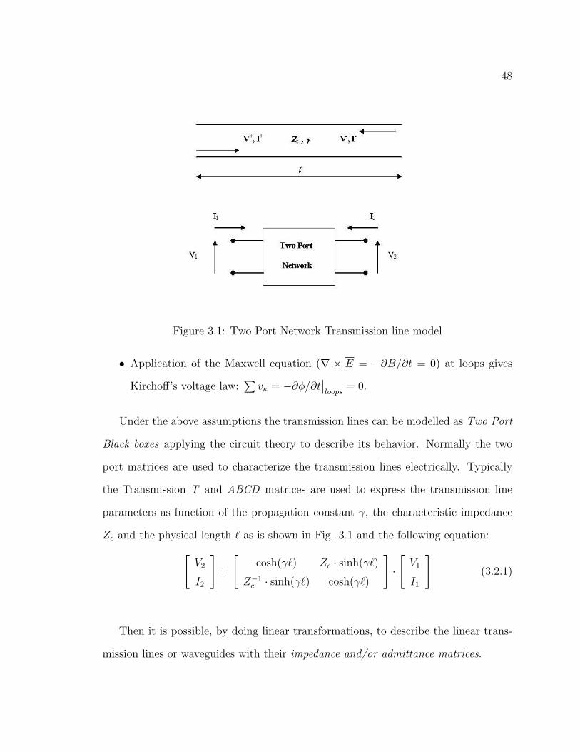
Figure 3.1: Two Port Network Transmission line model
• Application of the Maxwell equation (∇ × E = −∂B/∂t = 0) at loops gives
Kirchoff’s voltage law:∑
vκ = −∂φ/∂t∣∣loops
= 0.
Under the above assumptions the transmission lines can be modelled as Two Port
Black boxes applying the circuit theory to describe its behavior. Normally the two
port matrices are used to characterize the transmission lines electrically. Typically
the Transmission T and ABCD matrices are used to express the transmission line
parameters as function of the propagation constant γ, the characteristic impedance
Zc and the physical length ` as is shown in Fig. 3.1 and the following equation:
[V2
I2
]=
[cosh(γ`) Zc · sinh(γ`)
Z−1c · sinh(γ`) cosh(γ`)
]·[
V1
I1
](3.2.1)
Then it is possible, by doing linear transformations, to describe the linear trans-
mission lines or waveguides with their impedance and/or admittance matrices.
49
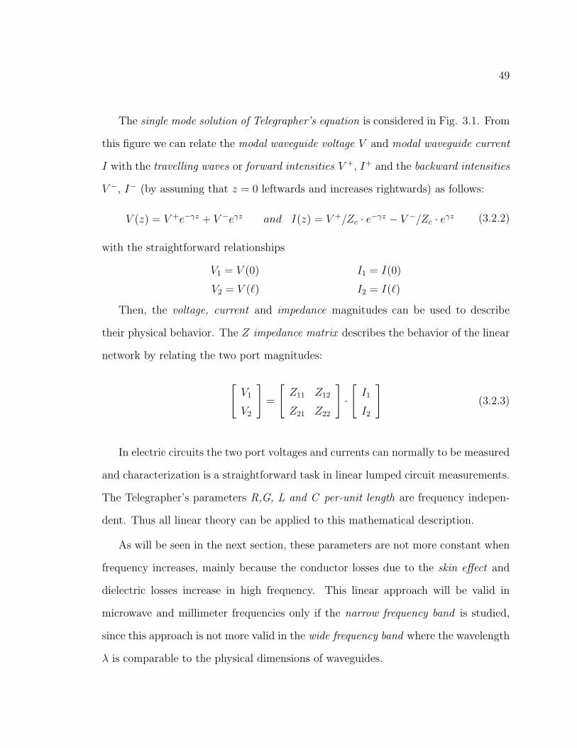
The single mode solution of Telegrapher’s equation is considered in Fig. 3.1. From
this figure we can relate the modal waveguide voltage V and modal waveguide current
I with the travelling waves or forward intensities V +, I+ and the backward intensities
V −, I− (by assuming that z = 0 leftwards and increases rightwards) as follows:
V (z) = V +e−γz + V −eγz and I(z) = V +/Zc · e−γz − V −/Zc · eγz (3.2.2)
with the straightforward relationships
V1 = V (0) I1 = I(0)
V2 = V (`) I2 = I(`)
Then, the voltage, current and impedance magnitudes can be used to describe
their physical behavior. The Z impedance matrix describes the behavior of the linear
network by relating the two port magnitudes:
[V1
V2
]=
[Z11 Z12
Z21 Z22
]·[
I1
I2
](3.2.3)
In electric circuits the two port voltages and currents can normally to be measured
and characterization is a straightforward task in linear lumped circuit measurements.
The Telegrapher’s parameters R,G, L and C per-unit length are frequency indepen-
dent. Thus all linear theory can be applied to this mathematical description.
As will be seen in the next section, these parameters are not more constant when
frequency increases, mainly because the conductor losses due to the skin effect and
dielectric losses increase in high frequency. This linear approach will be valid in
microwave and millimeter frequencies only if the narrow frequency band is studied,
since this approach is not more valid in the wide frequency band where the wavelength
λ is comparable to the physical dimensions of waveguides.

50
3.3 Characterization problem in microwaves and
millimeter waves
Classical waveguide circuit theory proposes an analogy between an arbitrary linear
waveguide circuit and a linear lumped electrical circuit. The lumped electrical circuit
is described by an impedance matrix, which relates the normal electrical currents and
voltages at each of its terminals, or ports. The waveguide circuit theory likewise
defines an impedance matrix relating the waveguide voltage and waveguide current
at each port. In both cases, the characterization of a network is reduced to the
characterization of its circuit components.
The general conditions satisfied by the impedance matrix are different in the two
cases. The waveguide voltage and current are highly dependent on definition and
normalization, in contrast to linear electrical circuits. The waveguide circuits are
described by travelling waves, not as lumped electrical ones.
As described in the last chapter, classical waveguide circuit theory is based on
defined waveguide voltage and waveguide current ; indeed these definitions rely upon
the electromagnetic analysis of a single and uniform waveguide [7]. Solutions of
Telegrapher’s linear equation are the eigenfunctions of the electromagnetic boundary
conditions. These eigenfunctions correspond to waveguide modes which propagate in
either direction with an exponential dependence on the axial coordinate.
A basic assumption of waveguide theory circuit is that at each port, a pair of
identical waveguides must be joined without discontinuity and must transmit only
a single mode, or a finite number of modes. When limited to a single mode, the
field distribution is completely described by these complex numbers indicating the

51
complex intensity of these two opposite travelling waves [34]. The waveguide voltage
and current related to the electric and magnetic fields−→E and
−→H of the mode, are
linear combinations of the two travelling waves. This linear relationship is function
of the characteristic impedance of the mode. Telegrapher’s equation is derived under
the following assumptions [41]:
• The conductors are perfect (resistivity % = 0) with uniform cross sections along
the line axis.
• The dielectric medium is homogeneous and isotropic characterized by the same
electrical permitivity ε and magnetic permeability µ along the line axis.
conductor losses and inhomogeneity are not taken into account and only TEM
mode waves are propagated.
The above assumptions are not more valid in the case of a lossy conductor that in-
validate the TEM field structure assumption because the line current flowing through
an imperfect line conductor generates a non zero electric field along the conductor
surface. However if the conductor losses are small, this resulting field structure is
almost TEM. This is referred to as the quasi-TEM assumption and, although the
transmission-line equations are no longer valid, they are nevertheless assumed to rep-
resent the situation for small losses through the inclusion of the per-unit-resistance
parameter R.
Another situation that invalidates the TEM assumptions is the presence of inho-
mogeneous cross section media around conductors, as in microstrip lines and coplanar
waveguides. The field velocity of propagation will be different in two different media
characterized respectively by ε1, µo and ε2, µo. The classical way of characterizing this

52
situation is to obtain an effective dielectric constant εeff , defined such that if the line
conductors are immersed in a homogeneous dielectric with a dielectric constant εeff ,
the velocities of propagation and all other attributes of the solutions for the original
inhomogeneous case will be the same.
Other implicit assumptions in the TEM characterization transmission-line equa-
tion are taken into account for its derivation. The distribution of lumped elements
along the line with infinitesimal section length means that the line lengths are elec-
trically long, i.e., much greater than a wavelength λ, and they are properly handled
by lumped-circuit characterization. However structures whose cross-sectional dimen-
sions are electrically large at the frequency of excitation will have, in addition to the
TEM field modes, other higher-order TE and TM modes of propagation simultane-
ously with the TEM mode. Therefore, the solution of Telegrapher’s equation does not
give the complete solution in the range of frequencies where these non-TEM modes
coexist on the line.
As an example of the complexity of the problem of propagation in high frequency
and inhomogeneous media the classical study on propagation in microstrip line given
by Hasegawa [24] is mentioned, where the existence of three different fundamental
modes of propagation as a function of the product of Si substrate resistivity and
the frequency is demonstrated. These three modes can be classified as the dielectric
quasi-TEM mode, the skin-effect mode and the slow-wave mode. In this work not only
is the influence of Si substrate resistivity on the mode propagation demonstrated, but
also heuristic proof of the frequency-substrate resistivity product influence on the
propagation modes.
All the assumptions and examples above mentioned show that there is no general

53
theory that applies and describes propagation, and therefore the characterization of
electromagnetic waves on lossy and inhomogeneous waveguides, that are the major
involved phenomena in microwave and millimeter range of frequencies. Thus the
treatment and modelling are based on an engineering approach assuming heuristic
arguments founded on low-frequency circuit theory that only serves to have a ”rough
estimate” of the actual behavior of microwave waveguides in the conditions indicated.
From the experimental point of view it is not possible to measure the modal
waveguide intensities in the microwave and millimeter range of frequencies. The
travelling waves are associated with the concept of voltage and current along the line
and generally are not available for measurements. As will be seen in the next section,
another linear combination of the waveguide intensities, the power waves, will be
used because they are easily able measurable by commercial VNA’s. Through these
power waves the waveguide or transmission line can be characterized directly from
the measurements of the Scattering matrix parameters that are linearly related to
them. In next section the major results of Scattering matrix theory will be presented
and the concepts used for metrology.

54
3.4 Scattering parameters theory review
The waveguide voltages and currents are never well defined in waveguides. These
magnitudes represent the vector sum of all mode contributions into the waveguide
interconnections and further they are very difficult or impossible to measure by con-
ventional measurement instruments. Historically it was more common to measure
power relationships in microwave fields. Although is not very intuitive, the travelling
waves concept is more closely related to the voltage or current along the line than to
the power in a stationary state.
If a circuit which terminates a line at the far end does not match the characteristic
impedance of the line, even if the circuit has no source at all, we have to consider
two travelling waves in opposite directions along the line. This makes the power
calculation twice as complicated. For this reason, when the main interest is in the
power relation between various circuits in which the sources are uncorrelated, the
travelling waves are not considered as the best independent variables to use for the
analysis.
A different concept of waves was introduced by Kurokawa [28], the power waves.
This new approach is theoretically equivalent to the characterization with Z or Y
matrices but it is more convenient because:
• the voltage and currents can not be directly measured in high frequency
• the power waves can be measured by VNA’s
• for wide bandwidths it is easier to obtain matched loads than open or short
circuits that are necessary to define the Z or Y matrices.

55
Figure 3.2: Power Waves and Reference Planes interpretation
To clear the concept a brief discussion follows. By considering a n-port electro-
magnetic structure as shown in Fig. 3.2 the power waves ai and bi at the different
reference planes in each port junction i of the structure can be defined as follows:
ai =Vi + ZiIi
2√| <(Zi) |
bi =Vi − Z∗
i Ii
2√| <(Zi) |
(3.4.1)
and by inverting the system,
Vi =1√
| <(Zi) |· (Z∗
i ai + Zibi) Ii =1√
| <(Zi) |· (ai − bi) (3.4.2)
where Vi and Ii are the voltage and the current flowing into the ith port of a
junction and Zi is the impedance looking out from the ith port. The positive real
value is chosen for the square root in the denominators.
In this definition each port is described by a reference plane transverse to a uniform

56
lossless waveguide leading to the junction and this reference plane is located at a
sufficient distance from the junction for far-field conditions to apply. Thus there is a
single mode propagated across each reference plane. The reference planes need to be
sufficiently far from any cross-section change of the uniform waveguide for evanescent
modes excited by the change to have decreased to negligible proportions at the plane.
The propagated mode need not be the same at all ports so different interfaces can be
described in these terms.
The physical meaning of power waves is related to the exchangeable power of a
generator. For this purpose, let us consider the equivalent circuit of a linear generator
as shown in Fig. 3.3, in which Zi is the internal impedance and E0 is the open
circuit voltage of the generator or Thevenin voltage. By applying the maximum
power transference theorem, the maximum power PL into the load ZL is given when
ZL = Z∗i then:
PL|max = Pa =|E0|2
4<(Zi)with <(Zi) > 0 (3.4.3)
The maximum power is called the available power of the generator, and is the
maximum power that the generator can supply to the load. If <(Zi) < 0 the eq.
(3.4.3) represents the exchangeable power which is finite but is not equal to the
maximum power. The voltage at the generator terminals is given by Vi = E0 − ZiIi.
Replacing it in the definition of ai from the power waves given by (3.4.1) and taking
the square of the magnitude, we have:
|ai|2 =|E0|2
4<(Zi)(3.4.4)

57
Figure 3.3: Equivalent circuit of a linear generator
which means the same as the available power of the generator, and if E0 = 0 then
ai = 0. If we develop the expression |ai|2 − |bi|2 in the definition (3.4.1) we have:
<ViI∗i = |ai|2 − |bi|2 (3.4.5)
The left-hand side of (3.4.5) represents the actual power transferred from the
generator to the load in the case where <(Zi) > 0. The generator sends the power
|ai|2 towards a load, regardless of the load impedance. If the load is not matched,
then ZL 6= Z∗i and a part of the incident power is given by |bi|2 so that the net power
absorbed by the load is equal to |ai|2−|bi|2. Associated to these incident and reflected
powers, are waves ai and bi respectively. These waves are considered the incident and
reflected powers because there is a linear relation between a′is and b
′is and this can
be used to advantageously define the Scattering parameters.
To define the Scattering matrix of a linear n-port network we consider the vectors
a, b, V and I at the ith port of the network respectively. Then a and b can be written

58
in terms of V and I as follows:
a = F (V + G · I), b = F (V + G∗T · I) (3.4.6)
Where ∗T denotes conjugate transposed matrix and:
F = diag(1/
√| <(Zi) |
), G = diag(Zi) (3.4.7)
Using the linear relation between V and I given by V = Z.I where Z is the
impedance matrix, the linear combination between a and b, the Scattering matrix S
is given by:
b = S · a (3.4.8)
and then, by equating (3.4.6),(3.4.7) and (3.4.8) we obtain the following relations
for S and Z matrices:
S = F (Z −G∗T )(Z + G)−1F−1
Z = F−1(I − S)−1(SG + G∗T )F(3.4.9)
Although the above definitions are related to the Zi impedance, this impedance
can be arbitrary, giving a different linear combination between a and b for different
impedances Zi. Therefore the Scattering matrix S is referred to a Zref reference
impedance by changing Zi by Zref in definition (3.4.1).
If we take an n-port structure as transmission line with characteristic impedance
Zci, from equation (3.2.2) we can express the power in the ith line as:
Pi = <ViI∗i = |V +
i |2/Zci − |V −i |2/Zci (3.4.10)
and by taking Zref = Zci in each ith port junction we can associate the power
waves with travelling waves in each ith junction as follows:
ai =V +
i√| <(Zci) |
bi =V −
i√| <(Zci) |
(3.4.11)

59
the total power into each ith port junction becomes:
Pi = |ai|2 − |bi|2 (3.4.12)
The equivalence between the Z and S matrices that fully characterize a n-port
electromagnetic structure was developed by starting from a power point of view.
A more modern definition of Scattering parameters is given by Marks and Williams
[34]. This work demonstrates that power waves as defined by (3.2.2) have no physical
meaning which the travelling waves do and they are only mathematical artifacts. The
power waves are equivalent to travelling waves only when the reference impedance Zref
is equal to the characteristic impedance Zi of the mode in each port.
When Zi varies greatly with frequency, as is often the case in lossy lines, the
resulting measurements using Zref = Zi may be difficult to interpret and a Zref = cte
is preferred. If Zref is chosen to be real, the power is given by (3.4.12). This is the
normal definition that is used in commercial VNAs, and as will be seen in the next
chapter, Zref is defined by a calibration process.

60
3.5 The Vector Network Analyzer
Vector Network Analyzer (VNA) system is intended as a complex electronic apparatus
that consents acquisition, management and presentation of data related to microwave
structures. Magnitude and phase characteristics of networks and components such as
filters, amplifiers, attenuators, and antennas are measured by VNAs.
Measurement of four scattering parameters is made by separating the incident
and reflected waves at two ports, Port 1 and Port 2, and then converting them to low
frequency to be sampled by the microprocessor system. Sampling and treatment of
the information is performed by an internal microprocessor system in the instrument’s
control unit that obtains data presentation and computes the numeric process. VNA
may be commanded by a remote computer through an external GPIB databus for
automatic instrumentation.
3.5.1 VNA General Description
A fully integrated Vector Analyzer System HP8510C [47] as used in this work is
composed by:
Source provides the RF signal. It is a Synthesized Sweeper.
Test Set separates the signal produced by the source into an incident signal, sent
to the device-under-test (DUT), and a reference signal against which the trans-
mitted and reflected signals are later compared. The test set also routes the
transmitted and reflected signals from the DUT to the receiver (IF/detector).
Command Unit includes the Display/Processor and the IF/Detector or Receiver.
The Receiver, together with the Display/Processor, processes the signals. Using

61
Figure 3.4: HP8510 Block Diagram (Agilent Technologies 2001)
its integral microprocessor, it performs accuracy enhancement and displays the
results in a variety of formats.
Peripherals system components that include peripheral devices such as a printer, a
plotter, and a disc drive. Measurement results and other kinds of information
can be sent to peripherals.
A Vector Network Analyzer simplified block diagram is presented in Fig. 3.4
3.5.2 Signal Source
In a measurement, the signal source is swept from the lower measurement frequency
to the higher measurement frequency using a linear ramp controlled by the VNA.

62
This sweep is called a ramp sweep and it gives the fastest update of the measurement
display. In step-sweep mode, the source is phase-locked at each discrete measurement
frequency controlled by the VNA. Useful bandwidths from 45 Mhz to 26 Ghz are
available and they can be enhanced to 40 Ghz.
Sweeper scan range and frequency can be selected by the VNA system bus. Dis-
crete frequencies measured range from 51 up to 801 samples in a single sweep. Fre-
quency resolution goes from 1 Hz at low frequency to 4 Hz at 26 Ghz. The sweeper
has an internal frequency reference and can be used an external reference as well.
Frequency resolution depends on the frequency reference used by.
3.5.3 Test Set
Test Set is the key component of the system and is designed to avoid the need to
reverse connections to the DUT when a reversed signal flow is required. Each test set
provides the following features:
• Input and output ports for connecting the device to test
• Signal separation for sampling the reference signal and test signals
• Test signal frequency to 20 MHz conversion
These functions can be integrated in a unique device, the S-parameter test set
that is connected to the Command Unit by an internal bus and to the Synthesized
Sweeper by coaxial connectors. Internally it has direct couplers, deviators, etc, that
are necessary to measure the scattering parameters and a frequency converter to
provide the signal frequency conversion to 20 Mhz.
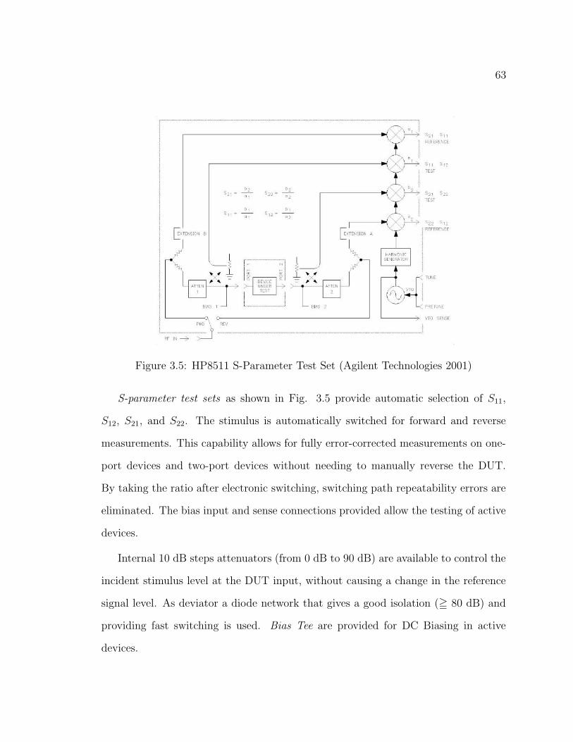
63
Figure 3.5: HP8511 S-Parameter Test Set (Agilent Technologies 2001)
S-parameter test sets as shown in Fig. 3.5 provide automatic selection of S11,
S12, S21, and S22. The stimulus is automatically switched for forward and reverse
measurements. This capability allows for fully error-corrected measurements on one-
port devices and two-port devices without needing to manually reverse the DUT.
By taking the ratio after electronic switching, switching path repeatability errors are
eliminated. The bias input and sense connections provided allow the testing of active
devices.
Internal 10 dB steps attenuators (from 0 dB to 90 dB) are available to control the
incident stimulus level at the DUT input, without causing a change in the reference
signal level. As deviator a diode network that gives a good isolation (= 80 dB) and
providing fast switching is used. Bias Tee are provided for DC Biasing in active
devices.

64
Figure 3.6: HP8511A Frequency Converter (Agilent Technologies 2001)
A frequency converter block diagram is shown in Fig. 3.6 and its conversion
procedure is performed by four diode samplers excited contemporarily by an impulse
burst whose frequency is selected to convert to 20 Mhz all amplitude and phase
characteristics of the four RF signals. One of the four signals becomes the reference
channel and the other three signals are phaselocked to it.
3.5.4 Command Unit
The Command Unit automatically manages all functions of the instrument. It re-
ceives the four 20 Mhz channels from the Test Set unit, and provides another hetero-
dyne down-conversion to 100 Khz for application in the detection and data processing
elements of the receiver.
Magnitude and phase relationships between the input signals are maintained
throughout the frequency conversion and detection stages, because the frequency

65
Figure 3.7: HP8510 DSP Block Diagram (Agilent Technologies 2001)
conversions are phase-coherent and the IF signal paths are carefully matched. Each
synchronous detector develops the real (X) and imaginary (Y) values of the reference,
or test signal, by comparing the input with an internally generated 100 kHz sine wave.
This method practically eliminates measurement uncertainty errors resulting from
drift offsets, and circularity. Each X,Y data pair is sequentially converted to digital
values and read by the central processing unit CPU. Accuracy of sampled data is
given by a 19 bit analog to digital conversion.
Digital data processing is performed by the CPU and a Math dedicated micropro-
cessor. Multiple operations, analysis, and data display presentation can be produced.
When error correction is selected, the raw data and error coefficients from the selected
calibration coefficient set are used in appropriate computations by a dedicated vector
math processor.

66
Corrected data are represented in time domain by converting from the frequency
domain to time domain using the inverse Fourier Chirp-Z transform technique. A
dedicated display processor asynchronously converts the formatted data for viewing
at a flicker-free rate on the vector-writing display. A block diagram of the VNA
Digital Signal Processing DSP is shown in Fig. 3.7.
3.6 Systematic error removal and VNA calibration
Vector Network Analyzers (VNA) find very wide application as primary tools in
measuring and characterizing circuits, devices and components. At higher frequencies
measurements pose significantly more difficulties in calibrating the instrumentation
to yield accurate results with respect to a known or desired electrical reference plane.
Characterization of many microwave components is difficult since the devices can-
not easily be connected directly to VNA-supporting coaxial or waveguide media. Of-
ten, the device under test (DUT) is fabricated in a non coaxial or waveguide medium
and thus requires fixturing and additional cabling to enable an electrical connection
to the VNA.
The point at which the DUT connects with the measurement system is defined as
the DUT reference plane and is the point where it is desired that measurements be
referenced. However, any measurement includes not only the DUT, but contributions
from the fixture and cables as well.
By increasing frequency, the electrical contribution of the fixture and cables be-
comes increasingly significant. In addition, practical limitations of the VNA in the
form of limited dynamic range, isolation, imperfect source/load match, and other
imperfections contribute to systematic errors of measurements.

67
A perfect measurement system would have infinite dynamic range, isolation, and
directivity characteristics, no impedance mismatches in any part of the test setup,
and flat frequency response. In practice, this ”perfect” network analyzer is achieved
by measuring the magnitude and phase of known standard devices, using this data
in conjunction with a model of the measurement system to determine error contri-
butions, then measuring a test device and using vector mathematics to compute the
actual response by removing the error terms.
The dynamic range and accuracy of the measurement is then limited by system
noise and the accuracy to which the characteristics of the calibration standards are
known. The following paragraphs describe the source of measurement errors, error
model definitions and error correction.
3.6.1 Measurement Errors
Network analysis measurement errors can be separated into three categories:
• Systematic Errors
• Random Errors
• Drift Errors
Drift errors can be compensated by an accurate project of the electronic and
mechanical parts of the systems and are minimized by a warm up period before to
start a measurement. Random errors are non-repeatable measurement variations
due to factors like system noise, connector repeatability, temperature variations, and
other environment and physical changes in the test setup between the calibration and
the measurement. These errors cannot be modelled and measured with an acceptable
68
degree or certainty, they are unpredictable and therefore cannot be removed from the
measurement, and produce a cumulative ambiguity in the measured data.
Systematic errors are repeatable and arise from imperfections within the VNA.
They include mismatch and leakage terms in the test setup, isolation characteristics
between the reference and test signal paths, and system frequency response. These
errors are the most significant at RF and microwave frequencies and they can be
largely removed by a calibration process. Causes of these errors are very complex and
they will be not discussed here. A full treatment of them is given in [43][47].
Such errors are quantified by measuring characteristics of known devices or stan-
dards. Hence systematic errors can be removed from the resulting measurement. The
choice of calibration standards is not necessarily unique. Selection of a suitable set of
standards is often based on such factors as ease of fabrication in a particular medium,
repeatability, and the accuracy with which the characteristics or the standard can be
determined.
The Systematic error correction process can be divided in:
• Error Model Definition
• Calibration Process
• Measurement of DUT and Error Correction or Deembedding
Error Models can be defined by their causes within the measurement instrument
or through a black box approach. The calibration process involves the actions needed
to identify correctly the error model parameters. Calibration is fully dependent on
the error model and on the number of parameters to be identified.

69
In the frequency domain, all known calibration techniques are based on the inser-
tion of standards or devices with well known electrical behavior on the place of DUT.
Measurement of standards gives the calculation of error model parameters. These
coefficients can be stored into a computer memory or into the VNA firmware to be
used to correct the DUT raw measurements mathematically within a deembedding
process.
In the following paragraphs the two most important approaches of Error Model
definitions will be discussed [43]. Historically the Twelve Terms Error Model is the
best known and it is the Error Model used internally by the VNA. The Error Box
Model approach was developed over the last two decades and it gives a more physical
meaning for the deembedding process, it also permits new and more accurate cali-
bration techniques to be followed by a computer outside the VNA. The last model
presented was adopted in this work and will be discussed with more attention. First
the Twelve Terms Error Model will be presented.

70
3.6.2 Twelve Terms Error Model
Historically the Twelve Terms Error Model was developed from the causes of mea-
surement uncertainties. They can be classified in the following categories:
• Directivity.
• Source Match.
• Load Match.
• Isolation.
• Tracking.
Directivity error is mainly due to the inability of the signal separation device
to absolutely separate incident and reflected waves. Residual reflection effects of
test cables and adapters give their contribution too in this uncertainty. Reflection
measurements are most affected by this error.
Source Match error is given by the inability of the source to maintain absolute
constant power at the test device input and by cable and adapter mismatches and
losses. This error is dependent on the relationship between input impedance of the
device under test DUT and the equivalent match of the source. It affects both trans-
mission and reflection measurements.
Load Match error is due to the effects of impedance mismatches between DUT
output port and the VNA test input. It is dependent on the relationship between the
output impedance of the DUT and the effective match of the VNA return port. It
affects both transmission and reflection measurements.

71
Isolation error is due to crosstalk of the reference and test signal paths, and
signal leakage within both RF and IF sections of the receiver. It affects high loss
transmission measurements.
Tracking error is the vector sum of frequency response, signal separation device,
test cables and adapters, and variations in frequency response between the reference
and test signal paths. It affects both transmission and reflection measurements.
The VNA provides different possibilities to measure these errors and they are de-
veloped in the literature [47][43]. The Full 2-Port Error Model or Twelve Terms Error
Model that provides full directivity, source match, load match , isolation and tracking
error correction for transmission and reflection measurements will be presented.
This model provides measurement accuracy for two-port devices requiring the
measurement of all four S parameters of the two-port device. There are two sets of
error terms, forward and reverse, with each set consisting of six error terms. Error
terms are the following:
• Forward Directivity EDF and Reverse Directivity EDR
• Forward Source Match ESF and Reverse Source Match ESR.
• Forward Load Match ELF and Reverse Load Match ELR.
• Forward Isolation EXF and Reverse Isolation EXR.
• Forward Reflection Tracking ERF and Reverse Reflection Tracking ERR.
• Forward Transmission Tracking ETF and Reverse Transmission Tracking ETR.
Twelve Terms Error Model Forward Set is shown in Fig. 3.8 and Reverse Set is
shown in Fig. 3.9.

72
SijA represent the actual DUT S-parameters and SijM are the measured S-
parameters . After a Calibration process the twelve error terms are calculated and
actual DUT parameters are given by the Error Correction Deembedding equations :
S11A =
[(S11M−EDF
ERF
).
[1+
(S22M−EDR
ERR
).ESR
]]−[(
S21M−EXFETF
).(
S12M−EXRETR
).ELF
]
(Deno)
S21A =
[1+
(S22M−EDR
ERR
).(
ESR−ELF
)].(
S21M−EXFETF
)(Deno)
S12A =
[1+
(S11M−EDF
ERF
).(
ESF−ELR
)].(
S12M−EXRETR
)(Deno)
S22A =
[(S22M−EDR
ERR
).
[1+
(S11M−EDF
ERF
).ESF
]]−[(
S21M−EXFETF
).(
S12M−EXRETR
).ELR
]
(Deno)
(3.6.1)
Deno =
[1 +
(S11M − EDF
ERF
).ESF
].
[1 +
(S22M − EDR
ERR
).ESR
]−
−[1 +
(S21M − EXF
ETF
).(S12M − EXR
ETR
).ELF .ELR
](3.6.2)

73
Figure 3.8: Twelve Terms Error Model Forward Set
Figure 3.9: Twelve Terms Error Model Reverse Set

74
3.6.3 Error Box Model (Eight-Term Error Model)
The most modern formulation of measurement errors is the physical model of system-
atic errors. The concept is based in a Ideal Free Error VNA, connected to the D.U.T
through two ”black boxes”, the Error Boxes A and B where all measurement errors
are concentrated. This concept permits a more systemic vision and error treatment
by becoming independent of their actual causes.
An Ideal Free Error VNA and two fictitious networks named Error Boxes define
the measurement system as shown in Fig. 3.10. The Error Boxes A and B take
into account the systematic error for the two ports in the measurements. Port A
and Port B represent the measurement reference planes, the error boxes contain the
contribution of the systematic errors and Port 1 and Port 2 represent the ideal error
free ports of the network analyzer.
Two basic hypotesis are assumed to define the Error Box Model : the isolation of
the ports and the linearity of the relation between the waves at each port. Isolation
of the ports is intended that the measured waves at each port depend only upon
the real waves at the same port, hence the signal path between the measured waves
a1m, b1m, a2m and b2m lays only inside the D.U.T., and not inside the test set (see
Fig. 3.11). This is quite reasonable and offers a dramatic simplification for the
calibration process. The majority of the calibrations algorithms known are based
on this assumption. Linearity allows to describe the model with standard two-port
parameters by indicating a straightforward relation between all magnitudes.
Based on the Error Box Model shown in Fig. 3.11, a mathematical description
that uses matrix notation is given. They can be defined as the error box S-matrices
EA and EB :

75
Figure 3.10: Ideal Free Error VNA and Error Boxes
[b1m
a1
]= EA ·
[a1m
b1
], with EA =
[e00
A e01A
e10A e11
A
](3.6.3)
[b2m
a2
]= EB ·
[a2m
b2
], with EB =
[e00
B e01B
e10B e11
B
](3.6.4)
In matrix notation, relationships at each port can be written as follows:
[b1m
a1m
]= Ta ·
[b1
a1
]and
[a2m
b2m
]= Tb ·
[a2
b2
](3.6.5)
The Ta is the Error Box A cascading matrix from left to right following the
signal path from Port 1 to Port 2, and Tb is the Error Box B transmission matrix

76
Figure 3.11: An interpretation of the Error Box Model
from right to left from Port 2 to D.U.T. Relationships between error box S-matrices
parameters and cascading and transmission matrices are given by:
Ta =1
e10A
·[−∆A e00
A
−e11A 1
]≡ 1
e10A
·Xa with ∆A = e00A · e11
A − e01A · e10
A (3.6.6)
Tb =1
e10B
·[
1 −e11B
e00B −∆B
]≡ 1
e10B
·Xb with ∆B = e00B · e11
B − e01B · e10
B (3.6.7)
The relationship between D.U.T. and error box parameters is given by equating
the measured and actual power waves through the matrix description of the model
as is shown in Fig. 3.11. The chain of matrices Tm represents the raw measurement
and is given by the following equation:
Tm = Ta · Td ·(Tb
)−1(3.6.8)

77
Thus the deembedding formula that gives Td, the D.U.T. cascading matrix , is obtained
just by inverting (3.6.8) as is shown:
Td =(Ta
)−1 · Tm · Tb = α−1 · (Xa
)−1 · Tm ·Xb (3.6.9)
with
α =e10
B
e10A
(3.6.10)
As can be seen from the above measurement system definition, the eight error terms
are totally defined by the parameters of the Error boxes A and B.
A different notation, as was presented by Ferrero in [19][20], will be used in this
work to describe error boxes in calibration algorithms. It is presented here by rewrit-
ing terms of the error box matrices and the deembedding formula as follows:
Ta = p ·Xa = p ·[
kp· a b
kp
1
], Tb = w ·Xb = w ·
[1 u
w
f uw· g
](3.6.11)
Td = α−1 · (Xa
)−1 · Tm ·Xb with α =p
w(3.6.12)

Chapter 4
Microwave and Millimiter WaveMeasurement Techniques
4.1 Introduction
In this chapter a calibration process will be defined and the more relevant calibration
techniques will be presented and discussed. To understand the calibration problem,
different techniques based in the Error Models definitions will be discussed. Limi-
tations of the different techniques will conduce to use them in diverse environments
(coaxial, microstrip lines, etc.). The deembedding process as the major characteriza-
tion procedure after a calibrated measurement will be presented in all cases.
4.2 VNA Calibration process
VNA Calibration process is intended as the actions needed to determine correctly
the numerical values of all the error model parameters at each frequency of interest.
This process is fully dependent upon the Error Model and the number of parameters
to identify.
78

79
Calibration techniques in frequency domain are based on the insertion of stan-
dard devices, with well known electrical characteristics, at the place of the D.U.T.
The measurement of these standard devices permits the identification of Error Model
parameters. These coefficients can be stored in the instrument’s memory or a re-
mote computer to be used to correct raw measurements through vector mathematics.
Modern VNAs are able to correct raw measurements in real time with a calibration
technique that is in the instrument’s firmware. Practical procedures are explained in
the HP 8510C Programmer’s Handbook [47].
Calibration techniques can be divided in two categories:
• Non redundant methods
• Redundant methods or self calibration
Non redundant methods are used where uncertainties about standard devices are
not admitted. These methods are based on the connection of well known standard
device fabricated specifically and grouped into Calibration Kits. There are different
Calibration Kits with standards as Short, Open, Thru, Line and Match; fabricated
in different technologies that are used in VNAs as coaxial, microstrip line, etc. The
best known non redundant method is SOLT and it is implemented in the commercial
VNA’s firmware.
Self calibration is based on system redundancy where not all parameters of stan-
dard devices need to be known because the number of independent measurements is
greater than number of parameters to be identified. Some electrical characteristics
of standard devices are found from the solution of the calibration process. Different
methods where developed, the most important is the TRL invented by Bianco et al

80
[4], with developments added by Engen and Hoer [11], Speciale [45],[46] and others;
the LRM developed by Eul and Schieck [13], and the modern UTHRU by Ferrero and
Pisani [19]. The following paragraphs will describe the more important calibration
techniques, their field of use and differences between them in terms of accuracy.
4.3 Non Redundant Methods
4.3.1 SOLT Calibration Technique
SOLT (Short-Open-Load-Through) is the earlier calibration technique and it is a pro-
cedure to calculate the Twelve Terms Error Model. Although fabrication techniques
favor SOLT standards in coaxial, it is difficult to implement them precisely in other
media such as microstrip and coplanar. So this calibration technique is suited to be
used with coaxial media. Known standards are short, open, load and through . There
are two kinds of measurements to determine the error terms: 1 - Port or reflection
measurement, and 2 - Port or transmission measurement.
In 1-Port measurements at Port 1 and Port 2 the Directivity, Source Match and
Reflection Tracking errors of backward and forward error models can be determined.
Standards used are a Short, an Open and a Matched Load. If D.U.T. is connected
to Port 1 EDF , ESF and ERF can be determined, instead if it is connected to Port
2 EDR, ESR and ERR can be determined. In Fig. 4.1 the 1 - Port Error model is
shown.
In the above model S11M is the measured reflection coefficient and S11A is the
actual one at Port 1. The relationship between them is given by Mason’s Rules as:
S11M = EDF +S11A · ERF
1− ESF · S11A
(4.3.1)

81
Figure 4.1: 1 - Port Error Model (Port 1)
By connecting standards with reflection coefficients as:
• known Short
• known Open
• known Load
it is possible to obtain a 3 equation system from (4.3.1) and to calculate EDF ,
ESF and ERF . Connecting the standards to Port 2 we have a similar 1 - Port model
as it is shown in Fig. 4.1. It is possible to calculate the error terms EDR, ESR and
ERR with the same assumptions as in Port 1 by the following equation:
S22M = EDR +S22A · ERR
1− ESR · S22A
(4.3.2)
In a 2 - Port measurement, connecting the source at Port 1 and the standard
through (Thru) between the two ports it is possible to determine ETF for the forward
case, and doing the same with the source at Port 2 ETR is obtained. Measured and
actual transmission coefficients are equated by:

82
S21M = S21A · ETF S12M = S12A · ETR (4.3.3)
Isolation terms EXF and EXR are measured by connecting as terminations two
loads at two ports and by placing them at the points at which the D.U.T. will be
connected. Then, with a transmission configuration, the isolation error coefficients
are measured. These terms are the part of incident wave that appears at the receiver
detectors without actually passing through the D.U.T.
Ideal standards with reflection coefficients like Γshort = −1, Γopen = 1 and Γload =
0, and transmission coefficients S21thru = 1 are impossible to achieve. Specially with
increasing frequency it is impossible to fabricate lossless standards and they will ex-
hibit differences from ideal behavior. Effects such as a nonzero length of transmission
line associated with each standard are acknowledged. If the electrical length of the
transmission line associated with the standards is short, losses become small and
attenuation α can be neglected without a significant degradation accuracy. Alterna-
tively, commercial VNAs describe transmission lines in terms of a delay coefficient
with a small resistive loss component. The open standard exhibits further imperfec-
tions and is often described in terms of a frequency-dependent fringing capacitance
expressed as a polynomial expansion. Standard models need to be provided by cali-
bration kits manufacturers.
SOLT Calibration accuracy is rigidly connected to standards behavior. Systematic
errors are removed by deembedding using equation (3.2.1) from the Twelve Terms
Error Model . Uncertainty of measurement is given by a residual systematic error
as non-ideal switching repeatability (switching error), non-infinite dynamic range,
cables stability and by casual errors.
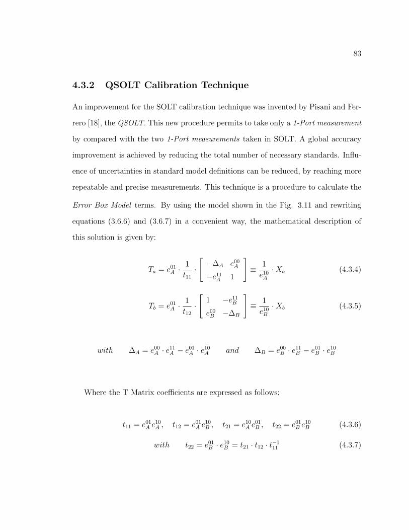
83
4.3.2 QSOLT Calibration Technique
An improvement for the SOLT calibration technique was invented by Pisani and Fer-
rero [18], the QSOLT. This new procedure permits to take only a 1-Port measurement
by compared with the two 1-Port measurements taken in SOLT. A global accuracy
improvement is achieved by reducing the total number of necessary standards. Influ-
ence of uncertainties in standard model definitions can be reduced, by reaching more
repeatable and precise measurements. This technique is a procedure to calculate the
Error Box Model terms. By using the model shown in the Fig. 3.11 and rewriting
equations (3.6.6) and (3.6.7) in a convenient way, the mathematical description of
this solution is given by:
Ta = e01A · 1
t11
·[−∆A e00
A
−e11A 1
]≡ 1
e10A
·Xa (4.3.4)
Tb = e01A · 1
t12
·[
1 −e11B
e00B −∆B
]≡ 1
e10B
·Xb (4.3.5)
with ∆A = e00A · e11
A − e01A · e10
A and ∆B = e00B · e11
B − e01B · e10
B
Where the T Matrix coefficients are expressed as follows:
t11 = e01A e10
A , t12 = e01A e10
B , t21 = e10A e01
B , t22 = e01B e10
B (4.3.6)
with t22 = e01B · e10
B = t21 · t12 · t−111 (4.3.7)

84
Figure 4.2: Ideal VNA and Error Box (Port 1)
Considering a 1-Port measurement as in SOLT but only in one port, Port 1 (Port
2), as indicated in Fig. 4.2, the two ports scheme is reduced to an ideal VNA followed
by an Error Box EA. It is demonstrated [18] that it is not necessary to know all four
Error Box parameters but only three: e00A , e11
A and the product t11 = e10A · e01
A . The
following relationship is given between the measured Γm and the actual Γa standard
reflection coefficients:
Γm = e00A +
e10A · e01
A · Γa
1− e11A · Γa
(4.3.8)
then, by connecting three known standards: short, open and load as in SOLT, it
is possible to have 3 independent equations and to calculate the desired error terms
e00A , e11
A and t11.
QSOLT measures a standard Thru in a 2-Port measurement with a known Tat
transmission matrix. By replacing expressions (4.3.4) and (4.3.5) into equation (3.6.8),
the relationship between the measured (subindex tm) and known Thru matrices with
Error Box terms are found to be:
Ttm = Xa · Tat ·X−1b (4.3.9)

85
then, because Xa was fully defined by the 1-Port measurement, the Error Box
transmission matrix Xb is determined by inverting (4.3.9) as:
Xb = T−1tm ·Xa · Tat (4.3.10)
The Xb Error Box terms are calculated with the following formulae:
e00B = X21
b · (X11b )−1
e11B = −X12
b · (X11b )−1
t22 = det(Xb) · (X11b )−2
t12 = (X11b )−1
t21 = t11 · det(Xb) · (X11b )−1
(4.3.11)
If an ”ideal” Thru (quasi ideal for typical applications as S21thru = S21thru ≈ 1) is
used as two-port device, the following equations apply:
S11tm = e00A + (t11 · e11
B ) · (1− e11A · e11
B )−1
S21tm = t21 · (1− e11A · e11
B )−1
S12tm = t12 · (1− e11A · e11
B )−1
S22tm = e00B + (t22 · e11
A ) · (1− e11A · e11
B )−1
(4.3.12)
Equating (4.3.7) with the above equation system (4.3.12) the Xb Error Box coef-
ficients are encountered:
e11B = (S11tm − e00
A ) · [t11 + e11A · (S11tm − e00
A )]−1
t21 = S21tm · (1− e11A · e11
B )
t12 = S12tm · (1− e11A · e11
B )
t22 = S21tm · S12tm · (1− e11A · e11
B )2 · t−111
e00B = S22tm − t22 · e11
A · (1− e11A · e11
B )−1
(4.3.13)

86
The QSOLT improvement is the reduction of the number of standards to be con-
nected from 7 to 4 without the need to take a Port 2 (Port 1) reflection measurement,
achieving more accuracy and reducing influence of uncertainties. This technique is not
implemented in the VNA firmware and needs to be performed on a remote computer.

87
4.4 Self Calibration or Redundant Methods
4.4.1 TRL technique
TRL (Thru Reflect Line) was invented by Bianco et al [4] and developed by Engen
and Hoer [11] as an improvement of TSD [45]. This technique is used to calculate the
terms of the Error Box model as was presented in Fig. 3.11. This solution is based
upon the measurement of a device in each of the two ports and two bilateral devices
connected between the ports:
• Thru: a piece of line with known length and characteristic impedance connected
to the two ports. Typically a zero length thru with an identity transmission
matrix is assumed.
• Reflect : a load (typically a piece of line opened or shorted) from which it is
only necessary to know the sign (phase) of its reflection coefficient within the
measurement frequency bandwidth. This device is alternatively connected to
Port 1 and Port 2.
• Line: a piece of line with the same characteristic impedance as the Thru but
with different length.
The goal of this solution is that it doesn’t rely on fully known standards and
it uses only three simple connections to completely characterize the error model.
The major problem in non-coaxial media is to separate the transmission medium
effects from the device characteristics. The accuracy of this measurement depends
on the quality of calibration standards. TRL calibration accuracy relies only on
the characteristic impedance of a short transmission line, and for this reason this
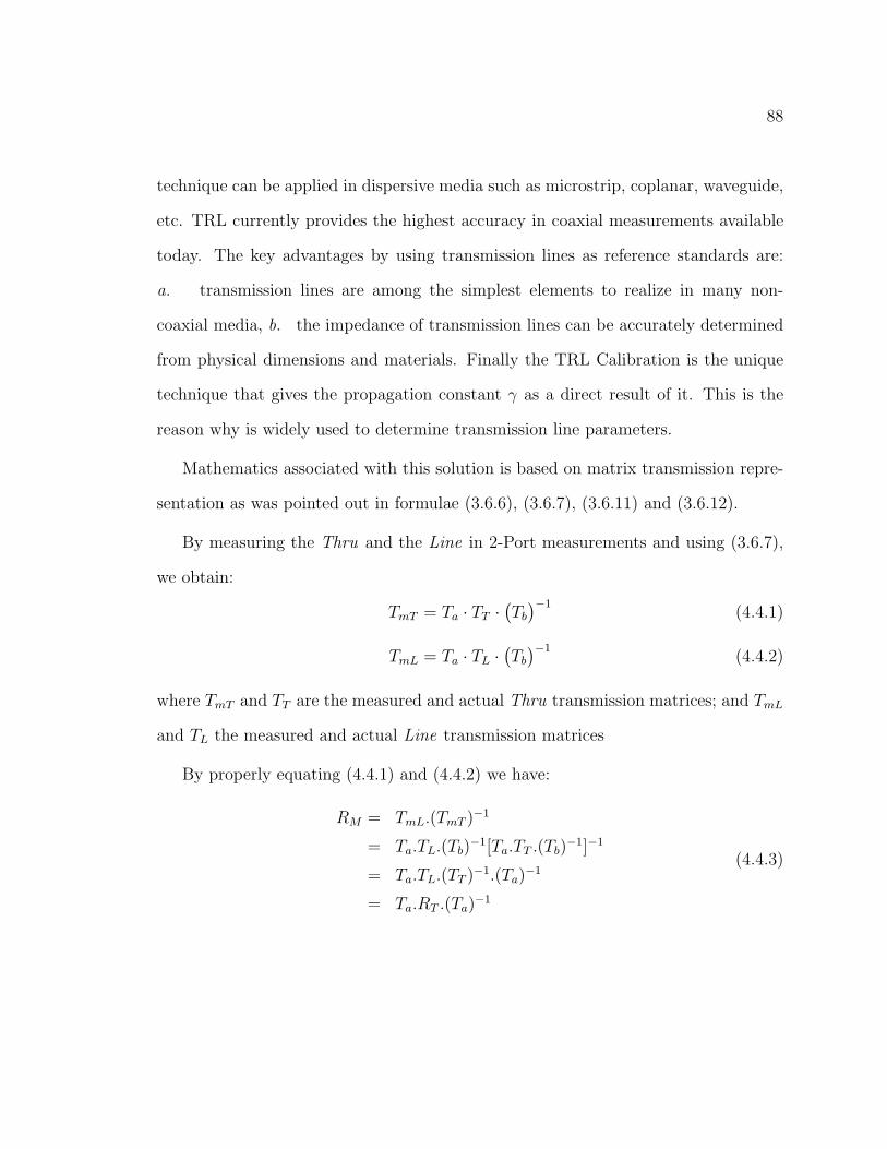
88
technique can be applied in dispersive media such as microstrip, coplanar, waveguide,
etc. TRL currently provides the highest accuracy in coaxial measurements available
today. The key advantages by using transmission lines as reference standards are:
a. transmission lines are among the simplest elements to realize in many non-
coaxial media, b. the impedance of transmission lines can be accurately determined
from physical dimensions and materials. Finally the TRL Calibration is the unique
technique that gives the propagation constant γ as a direct result of it. This is the
reason why is widely used to determine transmission line parameters.
Mathematics associated with this solution is based on matrix transmission repre-
sentation as was pointed out in formulae (3.6.6), (3.6.7), (3.6.11) and (3.6.12).
By measuring the Thru and the Line in 2-Port measurements and using (3.6.7),
we obtain:
TmT = Ta · TT ·(Tb
)−1(4.4.1)
TmL = Ta · TL ·(Tb
)−1(4.4.2)
where TmT and TT are the measured and actual Thru transmission matrices; and TmL
and TL the measured and actual Line transmission matrices
By properly equating (4.4.1) and (4.4.2) we have:
RM = TmL.(TmT )−1
= Ta.TL.(Tb)−1[Ta.TT .(Tb)
−1]−1
= Ta.TL.(TT )−1.(Ta)−1
= Ta.RT .(Ta)−1
(4.4.3)

89
andRN = (TmT )−1.TmL
= [Ta.TT .(Tb)−1]−1Ta.TL.(Tb)
−1
= Tb.(TT )−1.TL.(Tb)−1
= Tb.RS.(Tb)−1
(4.4.4)
Matrices RM and RT have the same eigenvalues as RN and RS given by the
following eigenvalue matrix:
Λ =
[λ1 0
0 λ2
](4.4.5)
The RM , RT , RN , RS eigenvector matrices are given by M , T , N and S respec-
tively, then it follows:
RM = M.Λ.M−1 = Ta.T.Λ.(T−1a .T−1) with Ta = M · T−1 (4.4.6)
RN = N.Λ.N−1 = Tb.S.Λ.(T−1b .S−1) with Tb = N · T−1 (4.4.7)
The Line transmission matrix with a length ` and propagation constant γ is given
by:
TL =
[e−γ.` 0
0 e+γ.`
](4.4.8)
By replacing the actual Thru and Line transmission matrices TL and TT in equa-
tion (4.4.3) we have:
RT = TL.T−1T = T.Λ.T−1 =
[e−γ.∆` 0
0 e+γ.∆`
]= Λ (4.4.9)
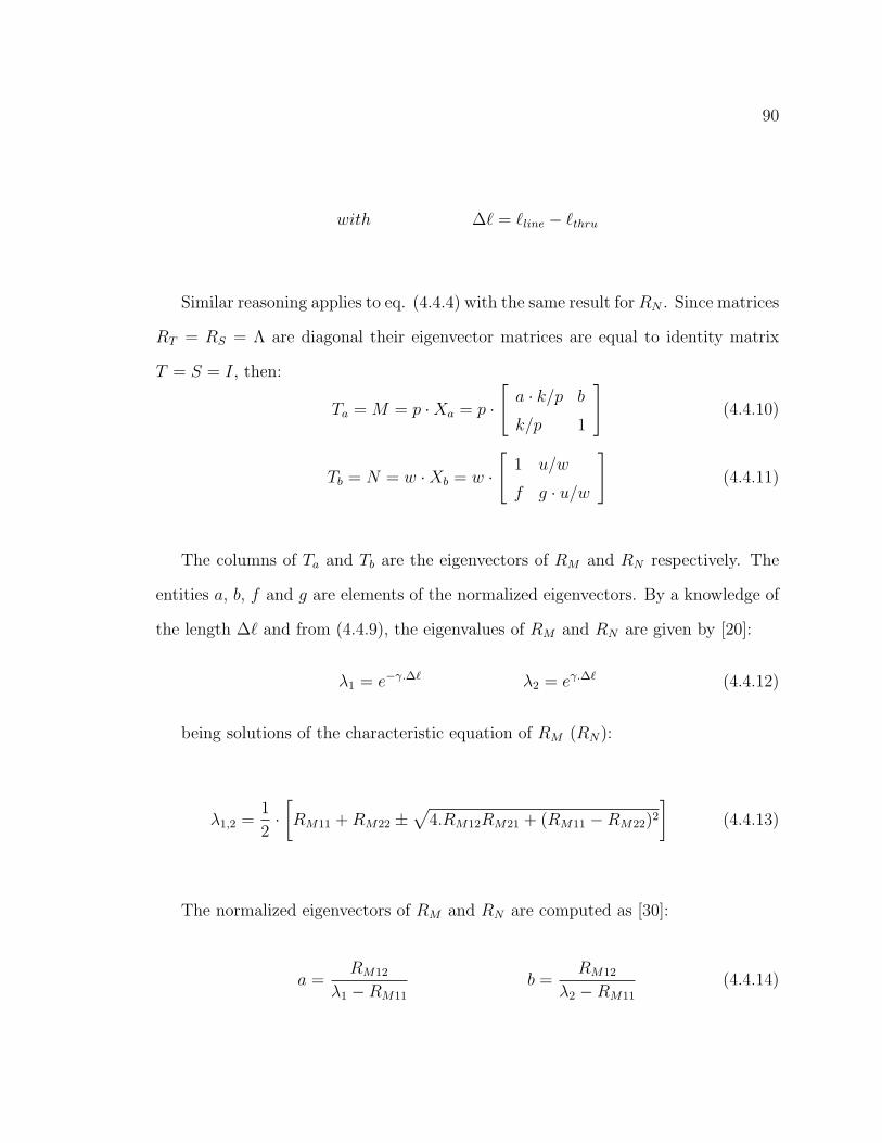
90
with ∆` = `line − `thru
Similar reasoning applies to eq. (4.4.4) with the same result for RN . Since matrices
RT = RS = Λ are diagonal their eigenvector matrices are equal to identity matrix
T = S = I, then:
Ta = M = p ·Xa = p ·[
a · k/p b
k/p 1
](4.4.10)
Tb = N = w ·Xb = w ·[
1 u/w
f g · u/w
](4.4.11)
The columns of Ta and Tb are the eigenvectors of RM and RN respectively. The
entities a, b, f and g are elements of the normalized eigenvectors. By a knowledge of
the length ∆` and from (4.4.9), the eigenvalues of RM and RN are given by [20]:
λ1 = e−γ.∆` λ2 = eγ.∆` (4.4.12)
being solutions of the characteristic equation of RM (RN):
λ1,2 =1
2·[RM11 + RM22 ±
√4.RM12RM21 + (RM11 −RM22)2
](4.4.13)
The normalized eigenvectors of RM and RN are computed as [30]:
a =RM12
λ1 −RM11
b =RM12
λ2 −RM11
(4.4.14)

91
f =λ1 −RN11
RN12
g =λ2 −RN11
RN12
(4.4.15)
From the measurement of the Reflect Γa at Port 1 (Γm1) and Port 2 (Γm2) the
following relationships are provided:
Γm1 =b + a · Γa · k/p
1 + Γa · k/pΓm2 =
f + g · Γa · u/w
1 + Γa · u/w(4.4.16)
The measured Thru input reflection coefficient SmT11 gives the following equation:
SmT11 =b− a · k/p · u/w
1− k/p · u/w(4.4.17)
By combining equations (4.4.16) and (4.4.17) the TRL algorithm calculates the
actual reflection coefficient Γa of the Reflect as follows:
Γa = ±√
(b− Γm1).(f − Γm2).(SmT11 − a)
(a− Γm1).(g − Γm2).(SmT11 − b)(4.4.18)
Reflect cannot be matched (Γa 6= 0). To solve the sign ambiguity the algorithm
needs a rough knowledge of the reflection phase.
By replacing eq. (4.4.18) in eqs. (4.4.16) and (4.4.17) the following coefficients
are obtained:
k
p=
Γm1 − b
(a− Γm1).Γa
u
w=
Γm2 − f
(g − Γm2).Γa
(4.4.19)

92
The multiplying factors p and w need not to be calculated but only their ratio
α = p/w. This property is clear by combining eqs. (4.4.10) and (4.4.11) into the raw
measurement fundamental equation (3.6.7) obtaining:
Tm = α.Xa.Td.(Xb)−1 =
p
w·[
a · k/p b
k/p 1
]· Td ·
[1 u/w
f g · u/w
]−1
(4.4.20)
From the Thru measurement, the transmission coefficient SmT21 is obtained and
the α coefficient is given by:
α =u/w · (g − f)
(1− u/w · k/p) · SmT21
(4.4.21)
As subproducts of the TRL Calibration the propagation constant γ of the Line
and the actual reflection coefficient Γa of the Reflect are calculated.
There are important features to consider with this technique:
• The reference plane is put in the middle of the Thru.
• The reference impedance of the measurement system is defined by the charac-
teristic impedance of the Line.
• The TRL has frequency limitations and it needs multiple lines to cover a broad-
band. It is necessary that ∆` = `line−`thru 6= n·λ/2 because at these frequencies
the algorithm doesn’t work and produces ill conditioned matrices.

93
Figure 4.3: Thru - Line Setup Measurement Reference Planes
To make a TRL Calibration it is necessary to take into account some practical
considerations:
• The electrical length of the Line section should be λ/4 or 90 in the middle
of the measurement span frequency and a phase difference between 20 and
160 along the same span assures that, the TRL algorithm is in a convergency
bandwidth, sufficiently far from the 6= n · λ/2 frequencies.
• TRL is frequency limited to bandwidths no larger than 8:1. For wider band-
widths, ulterior lines are employed to split the band.
• To measure the Line its position needs to be centered with respect to the center
of the Thru and reference planes will be re-positioned as shown in Fig. 4.3.
• Within a planar measurement with an accurate fixture setup is required to have
the proper position of microprobes with respect to the devices. To assure that
the reference planes will be just besides the edge faces of the D.U.T. a piece of

94
Figure 4.4: D.U.T. Setup Measurement Fixture
Thru with a length of 1/2.`thru has to be added to both sides of the D.U.T.
centering it as shown in Fig. 4.4.
• If the Thru is not ideal then matrix T 6= I. If T matrix is diagonal the
consequence is a different reference plane than ideal. This it is taken into ac-
count with the considerations shown in Fig. 4.4. If T matrix is complete, then
Line and Thru have different characteristic impedances and the reference
impedance of the system will be different from the Line. Heuristic consider-
ations are made to solve this situation by taking a compromise value of the
reference impedance as the geometric mean of the Thru and Line character-
istic impedances Zref ≈√
Zthru · Zline .

95
4.4.2 RSOL (UTHRU) technique
This technique developed by Pisani and Ferrero [19] is an innovative self calibration
solution where the greatest obstacle in modern techniques like TRL or LRM that is
the full knowledge of at least one two-port network, the Thru standard is surpassed.
In many applications this Thru standard can not be completely known. An example
of this is the case where it is not possible to connect directly the two probes, then
it is necessary to have as short as possible Thru that guarantees low losses and easy
modelling. An example of this is the case of two port on-wafer devices with unaligned
ports or having a 90 angle between them as shown in Fig. ??, a very important
situation in today’s actual RF ICs.
RSOL (reciprocal - short - open - load) technique doesn’t requires any particular
Thru knowledge. This procedure is based on the two ports Error Box model where
any reciprocal two-port can be used as Thru . The unique requirement of the Thru
standard is reciprocity and a rough knowledge of its transmission coefficient S21 phase
shift.
Associated mathematics with this solution is given by Error box model equations
(3.6.6), (3.6.7), (3.6.9) and (3.6.10) that are rewritten here for the sake of simplicity:
Ta =1
e10A
·[−∆A e00
A
−e11A 1
]≡ 1
e10A
·Xa with ∆A = e00A · e11
A − e01A · e10
A
Tb =1
e10B
·[
1 −e11B
e00B −∆B
]≡ 1
e10B
·Xb with ∆B = e00B · e11
B − e01B · e10
B
Td =(Ta
)−1.Tm.Tb = α−1.
(Xa
)−1.Tm.Xb with α =
e10B
e10A

96
As in the SOLT calibration technique it is necessary to take two 1-Port Mea-
surements to obtain the error coefficients of Xa and Xb matrices. The relationship
between the measured Γm and the actual Γa standard reflection coefficients at Port
1 is the following:
Γm = e00A +
e10A · e01
A · Γa
1− e00A · Γa
(4.4.22)
and by connecting three known standards: short, open and load , it is possible to
have 3 independent equations and to calculate the desired error terms e00A , e11
A and
the product e10A · e01
A . The same reasoning applied at Port 2 gives the error terms e00B ,
e11B and the product e10
B · e01B . With these error terms it is straightforward to obtain
∆A and ∆B.
Finally, the coefficient α is obtained by connecting a reciprocal unknown two-port
network between the ports. By applying the reciprocity properties, the transmission
matrix of a reciprocal unknown Thru has an unitary determinant. From (3.6.5), it
follows:
det(Tm) = α2 · det(XA) · det(XB)−1 (4.4.23)
therefore,
α = ±√
det(Tm) · det(XB)
det(XA)(4.4.24)
The sign ambiguity is solved as follows. Let
Y = (XA)−1 · Tm ·XB (4.4.25)

97
which is fully known from the above measurements. Then, by applying (3.6.5) the
Thru S21 scattering parameter is given by:
S21thru =α
Y22
(4.4.26)
From the above equation, a rough knowledge of the Thru S21 phase shift is all
that is necessary to solve the α sign ambiguity.
This solution allows to calibrate the two ports although they have identical sex
connectors or different port transitions as coaxial in Port 1 and Port 2 directly an
on-wafer probe, without complicated models for the transitions or elaborated deem-
bedding procedures. Accuracy of this technique is comparable to modern LRM
technique as proven by Pisani and Ferrero [19].

Chapter 5
Calibration & Measurement Tool
5.1 Introduction
As an original contribution, a Calibration and Measurement Tool based on the
TRL algorithm was developed. This tool uses the capacity of the VNA HP8510C to
be connected to a remote computer through an IEEE 488.2 interface. The program
was developed in MATLAB code and it runs in different platforms giving a versatile
use. Interesting features were implemented into this tool. Full TRL calibrations can
be performed through the use of an easy-to-use GUI designed to this effect. Deem-
bedding and plot of results are available for the user. Further, it is possible to perform
the Uploading of Twelve Error coefficients in the VNA. This feature allows a unique
calibration in a remote computer and store it into the measurement instrument, giv-
ing a powerful utility for repetitive measurements. In the following paragraphs a
description of the tool is provided. An example of calibration is presented and is
compared with other calibration techniques. Original equations for the equivalence
between the Twelve Error coefficients and the Error box model are presented for the
first time in literature.
98
99
5.2 MATLAB Calibration & Measurement Tool
This tool exploits the MATLAB Instrument Toolbox by connecting the computer to
a remote measurement instrument through a GPIB card and an IEEE 488.2 bus for
virtual instrumentation. This feature permits to develop a code program in a easy
way through the only configuration of the computer card by the user, without taking
into account low level signals.
A GUI (General User Interface) was implemented to achieve an easy interaction
with the user. All features of the software are performed by interaction with the
GUI and proper callback functions, giving a structured and efficient code. The code
program uses these functions to subdivide tasks in simple routines that pass inputs
and results as function arguments. In the Appendix A a User Guide is provided where
all user actions are fully explained. This particular tool was developed by dividing
the main routines in two functional blocks:
• Environment Values
• Calibration and Measurement
The Environment Values is a block that permits the user to configure a particu-
lar calibration and measurement. The user can define these environment values by
writing the start and stop frequencies, number of samples, source RF power and the
average factor. The average factor is defined because the tool uses the Step Mode of
the VNA by phase locking single sample frequencies and averaging single frequency
measurement. By pressing a button all user’s values are automatically communicated
to the instrument.

100
Calibration and Measurement is the heart of the program and is divided in three
functional parts:
• TRL Calibration
• DUT and Deembedding
• Uploading and calibrated measurement
The TRL Calibration is performed by the measurement of the known Reflect
standard at Port 1 and Port 2 and the LINE and THRU standards. In this block
the user gives the software a rough knowledge of the phase of the Reflect to be used
in the TRL algorithm. When the four standard measurements have been made, the
TRL algorithm is implemented calculating the Error Box parameters.
Once TRL standards have been measured, a DUT measurement of raw data
can be taken. After this, automatically DUT Corrected data are calculated by the
Deembedding procedure as was explained for the TRL algorithm in the last chapter.
Lastly can be performed the uploading of the twelve error terms to the measure-
ment instrument, using an internal routine that calculates the equivalence between
the Error Box model and Twelve Terms that is in the VNA. This equivalence was
developed explicitly for the first time in this work. Once the uploading is achieved, a
calibrated measurement can be performed by using the uploaded twelve terms coef-
ficients.
All standard, DUT, DUT Corrected data and calibrated measurements, are stored
into files in Touchstone format and their names can be changed by the user through
the GUI. The tool permits easy calibration and measurement to be performed as well

101
as deembeded data for characterization. By applying TRL Calibration, the propa-
gation constant γ and the actual Reflect standard Γa are measured. The following
paragraph describes the implementation of the TRL algorithm in the tool as well as
the equivalence between Error Box model and Twelve Terms , with the calculated
terms to be uploaded.

102
5.3 Calibration & Measurement program
The calibration & measurement tool implements the TRL algorithm for calibration.
Formulae used for this algorithm are given. Using the Error Box model as shown in
Fig. 3.10 and Fig. 3.11, a description of the algorithm will be given.
Classical error model representations as given in Marks’ work [36] take into ac-
count unbalanced and imperfect switching by two switch terms, that represent the
reflection coefficients ΓF and ΓR of the port termination in the forward and backward
stimulation configurations as shown in Fig. 5.1.
They represent the switch error contribution (this model is only presented for
convenience and its parameters will be not explained. A total equivalence with our
representation stems from X = Ta, Y = Tb and T = Td. The α and β coefficients are
constants that comprise a different presentation of the same model).
In our work these reflection coefficients are omitted because the Switch Correction
algorithm that permits to minimize (and practically eliminated) the switching error
was implemented.
Implementing the Switch Correction algorithm simplifies the Error model and the
switching error contribution is eliminated. To explain the algorithm’s implementation
a brief explanation of the Switch Correction algorithm as implemented in our program
will be given.
5.3.1 Switch Correction algorithm
The TRL Calibration and DUT measurements are made by applying the Switch
Correction algorithm that calculates the scattering parameters by measuring the 4
power waves.

103
Figure 5.1: R. Marks Error-Box Error Model of a Three-Sampler VNA
The RF source signal is injected at Port 1 and Port 2 alternatively. It allows to
minimize the isolation error, assuming a zero value for the Error Box Model calcu-
lation. The algorithm is applied to a Four-Sampler VNA. When the signal source is
applied to Port 1, as can be seen Fig. 5.2, the relationship between power waves and
the measured scattering matrix [Sm] is given by:
[b′1m
b′2m
]=
[Sm11 Sm12
Sm21 Sm22
]·[
a′1m
a′2m
](5.3.1)
where the′supraindex is a remark for power waves measured with the signal source
applied at Port 1. Then, applying the signal source to Port 2, a second measurement
of the power waves is made and the relationship between these power waves becomes:
[b′′1m
b′′2m
]=
[Sm11 Sm12
Sm21 Sm22
]·[
a′′1m
a′′2m
](5.3.2)

104
Figure 5.2: Measurement System for two 2-Port networks
where the′′
supraindex is a remark for power waves measured with the signal
source applied at Port 2.
The measured scattering parameters matrix [Sm] is now found by combining
(5.3.1) and (5.3.2) as follows:
[Sm11 Sm12
Sm21 Sm22
]=
[b′m1 b
′m2
b′′m1 b
′′m2
]·[
a′m1 a
′m2
a′′m1 a
′′m2
]−1
(5.3.3)
This procedure is followed for all 2-Port devices to be measured, giving the actual
measured S-parameters with the switch error corrected by (5.3.3), balancing the two
ports switching.

105
5.3.2 TRL algorithm and DUT deembedding
The TRL Calibration algorithm is implemented by measuring the 1-Port Reflect at
Port 1 and Port 2, and by the two port measurements of LINE and THRU. All the
measurements performed by the tool are made using the Switch Correction algorithm.
For each frequency sample the following steps are performed.
First the TmT and TmT matrices (eqs. 4.4.1 and 4.4.2) are calculated by trans-
forming the THRU and LINE measured S-matrices to cascade T matrices. Then RM
and RN are obtained as:
RM = TmL.(TmT )−1 RN = (TmT )−1.TmL (5.3.4)
By using the MATLAB function eig, the eigenvectors matrices M and N respec-
tively of RM and RN are calculated and given as:
[M ] = eig(RM) =
[M11 M12
M21 M22
][N ] = eig(RN) =
[N11 N12
N21 N22
](5.3.5)
By using the conclusions of (4.4.9) where matrices RT = RS are diagonal, the
coefficients of Error Box model are given by:
Ta = M = p ·Xa =
[ka pb
k p
]Tb = N = w ·Xb =
[w u
wf ug
](5.3.6)

106
And the a, b, f and g coefficients are calculated as follows:
a =M11
M21
b =M12
M22
f =N21
N11
g =N22
N12
(5.3.7)
From the measurement of the Reflect at Port 1 (Γm1) and Port 2 (Γm2), and the
measured Thru input reflection coefficient SmT11; the actual Reflect Γa is calculated
by solving (5.3.8) as:
Γa = ±√
(b− Γm1).(f − Γm2).(SmT11 − a)
(a− Γm1).(g − Γm2).(SmT11 − b)(5.3.8)
Using the above result and data, the coefficients k/p and u/w are calculated by
the algorithm as:
k
p=
Γm1 − b
(a− Γm1).Γa
u
w=
Γm2 − f
(g − Γm2).Γa
(5.3.9)
Finally from the above results and the measured Thru transmission coefficient
SmT21, the α coefficient is calculated as:
α =u/w · (g − f)(
1− u/w · k/p) · SmT21
(5.3.10)
The above calculations provide all the Error Box model coefficients that are nec-
essary to get the corrected data from the DUT raw data through the deembedding
process.

107
The DUT is measured in the same way as the other two port devices. Once
this measurement is achieved, the software has all the necessary data to perform
the deembedding calculation for the actual DUT data. With the Error Box model
coefficients and the DUT raw data, the deembedding formula is calculated by the
program as:
Td = α−1 · (Xa
)−1 · Tm ·Xb (5.3.11)
5.3.3 Uploading and calibrated measurements
This utility is useful to perform repeated measurements with the same calibration.
It permits the user to do a calibration on a remote computer and to upload the
calculated coefficients to the VNA memory. This feature calculates the equivalent
Twelve terms of the VNA model from the Error Box model coefficients. In our work
an equivalence between the two models was implemented and explicit expressions of
Twelve Terms Error Model are given for the fist time in literature.
The equivalence is based on the Error Model of a four sampler VNA developed
by Marks [36], shown in Fig. 5.2, and another equivalence given in [3]. In this model
the Error Boxes are given by X and Y as cascade matrices respectively, the actual
DUT as the T matrix and the measured raw data as Tm. By combining and equating
properly the presented formulae in this model, the following equation results:
Tm = β/α · 1
ERR
[ERF − EDF .ESF EDF
−ESF 1
]T
[ERR − EDR.ESR ESR
−EDR 1
](5.3.12)

108
Figure 5.3: Error Model of a Four Sampler VNA
where the α coefficient is totally different from the other one given in the above
equation (5.3.11). To show the equivalence between this model with coefficients of
the Twelve Terms Error Model expressed, we first rearrange the equation (4.4.20)
properly and we set Td = T . Then, an equivalent equation to (5.3.12) is found, using
uniquely Error Box model coefficients are written:
Tm =p/w
u/w · (g − f)·[
a · k/p b
k/p 1
]· T ·
[−g · u/w u/w
−f 1
](5.3.13)
Properly equating the terms expressed in (5.3.12) and (5.3.13) we find an equiva-
lence for the first six terms expressed as follows:
EDF = b
EDR = f
ESF = −k/p
ESR = −u/w
ERF = k/p · (a− b)
ERR = u/w · (g − f)
(5.3.14)
To find the equivalence of the last terms from the Twelve Terms Error Model we

109
Figure 5.4: Twelve Terms Error Model - Forward and Backward sets
use the formulae extracted from the model shown in Fig. 5.3 and given by R. Marks
in [36] as follows:
β/α =ETR
ERF + EDF · (ELR − ESF )(5.3.15)
α/β =ETF
ERF + EDR · (ELF − ESR)(5.3.16)
By replacing the results of (5.3.14)in (5.3.15) and (5.3.16) and equating properly
we find that:
ETR = p/w · [k/p · a + b · ELR] (5.3.17)
ETF = (p/w)−1 · [u/w · g + f · ELF ] (5.3.18)

110
With the assumptions made in [36] that switch coefficients do not have any im-
portant influence, (ΓF = ΓR = 0) (fact that is reasonable in our case because the
Switch Correction algorithm was applied to all the two port measurements), we find
the following equivalences:
ELF = ESR and ELR = ESF (5.3.19)
Another important assumption used in all Error Box model formulations is that
the isolation of the error boxes, and thus the forward and reverse isolation terms on
the Twelve Terms Error Model, are assumed to be null EXF = EXR = 0.
Replacing the terms of (5.3.19) in (5.3.17) and (5.3.18) and by equating we find
the last equivalences for ETR and ETF :
ELF = −u/w
ELR = −k/p
ETF = (p/w)−1 · u/w · (g − f)
ETR = (p/w) · k/p · (a− b)
EXF = 0
EXR = 0
(5.3.20)
From the above expressions (5.3.14) and (5.3.20), the software calculates the
Twelve Terms Error Model from the Error Box model coefficients presented in our
work. After that, they can be uploaded into the memory of the instrument by the user
to perform automated calibrated measurements. Therefore with a single calibration,
it is possible to perform repeated calibrated measurements using this utility and the
deembedding process is performed automatically by the VNA using the Twelve Terms
calculated by the user calibration algorithm.
111
5.4 Coaxial Experimental Results
TRL Calibration and a DUT measurement with a Coaxial Kit were performed and
compared with another on board SOLT Calibration as an example of the automated
features that the software brings.
The selected DUT was a precision 6 dB SMA Coaxial Attenuator. A 30 mm length
Rigid Coaxial SMA connector was used as the LINE. As REFLECT the OPEN Loads
of a Mauryr Coaxial Calibration Kit were used.
With another feature of the program, the attenuation constant α of the LINE and
the ηeff = c/vph coefficient were calculated. Plots of the different magnitudes of Raw
data, Corrected DUT data and the actual Reflect coefficient Γa are provided.
From the plot of the DUT Reflection Coefficient S11 the DUT corrected data from
the TRL Calibration performed by the tool can be seen in a smooth trace. Around
this plot there is the trace (with ”ripple” wave form) of the DUT corrected data given
by the calibration performed with the uploaded 12 error terms calculated by the tool.
The other two calibration performed by the VNA firmware, the on board SOLT have
more irregular traces.
The graph highlights that the phase of DUT transmission coefficient S21 corrected
by the TRL Calibration performed has a linear behavior along the entire bandwidth
as opposed to the same coefficient S21 performed with a SOLT on board calibration
(performed with the same standards as the tool TRL calibration) that has phase skips
in the band.
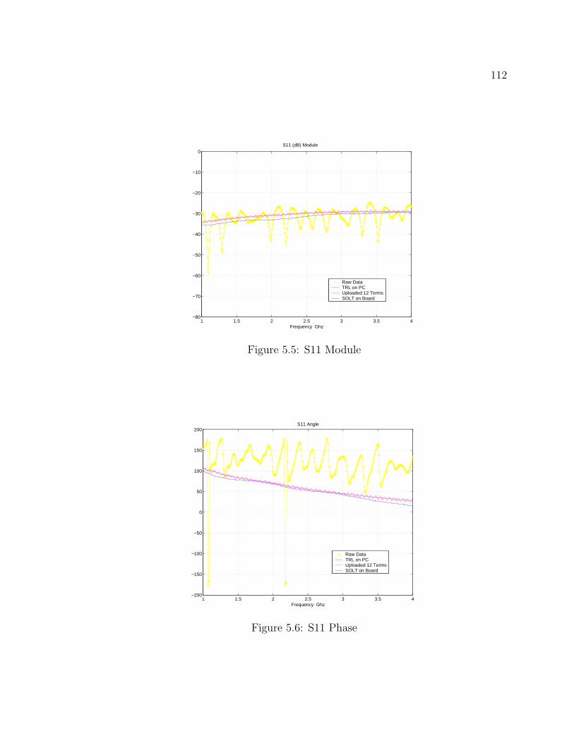
112
1 1.5 2 2.5 3 3.5 4−80
−70
−60
−50
−40
−30
−20
−10
0S11 (dB) Module
Frequency Ghz
Raw DataTRL on PCUploaded 12 TermsSOLT on Board
Figure 5.5: S11 Module
1 1.5 2 2.5 3 3.5 4−200
−150
−100
−50
0
50
100
150
200S11 Angle
Frequency Ghz
Raw DataTRL on PCUploaded 12 TermsSOLT on Board
Figure 5.6: S11 Phase
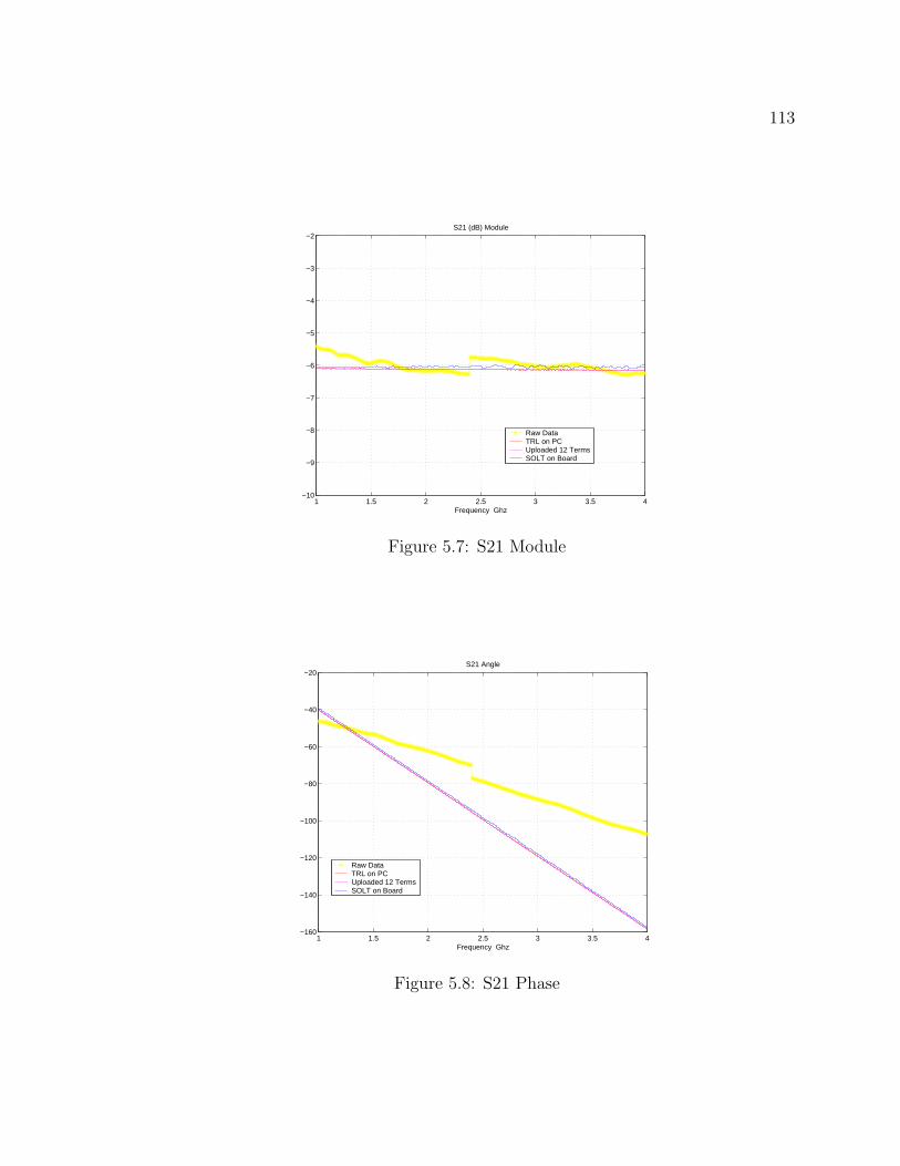
113
1 1.5 2 2.5 3 3.5 4−10
−9
−8
−7
−6
−5
−4
−3
−2S21 (dB) Module
Frequency Ghz
Raw DataTRL on PCUploaded 12 TermsSOLT on Board
Figure 5.7: S21 Module
1 1.5 2 2.5 3 3.5 4−160
−140
−120
−100
−80
−60
−40
−20S21 Angle
Frequency Ghz
Raw DataTRL on PCUploaded 12 TermsSOLT on Board
Figure 5.8: S21 Phase
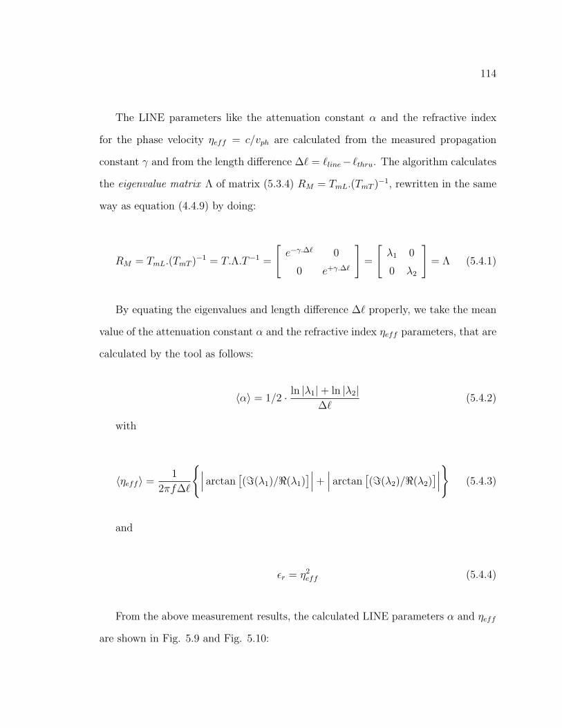
114
The LINE parameters like the attenuation constant α and the refractive index
for the phase velocity ηeff = c/vph are calculated from the measured propagation
constant γ and from the length difference ∆` = `line− `thru. The algorithm calculates
the eigenvalue matrix Λ of matrix (5.3.4) RM = TmL.(TmT )−1, rewritten in the same
way as equation (4.4.9) by doing:
RM = TmL.(TmT )−1 = T.Λ.T−1 =
[e−γ.∆` 0
0 e+γ.∆`
]=
[λ1 0
0 λ2
]= Λ (5.4.1)
By equating the eigenvalues and length difference ∆` properly, we take the mean
value of the attenuation constant α and the refractive index ηeff parameters, that are
calculated by the tool as follows:
〈α〉 = 1/2 · ln |λ1|+ ln |λ2|∆`
(5.4.2)
with
〈ηeff〉 =1
2πf∆`
∣∣∣ arctan[(=(λ1)/<(λ1)
]∣∣∣ +∣∣∣ arctan
[(=(λ2)/<(λ2)
]∣∣∣
(5.4.3)
and
εr = η2eff (5.4.4)
From the above measurement results, the calculated LINE parameters α and ηeff
are shown in Fig. 5.9 and Fig. 5.10:
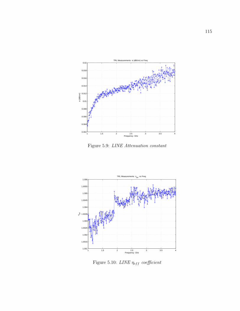
115
1 1.5 2 2.5 3 3.5 40.002
0.004
0.006
0.008
0.01
0.012
0.014
0.016
0.018
0.02TRL Measurements α (dB/cm) vs Freq
α (d
B/c
m)
Frequency Ghz
Figure 5.9: LINE Attenuation constant
1 1.5 2 2.5 3 3.5 41.001
1.0015
1.002
1.0025
1.003
1.0035
1.004
1.0045
1.005
1.0055
1.006
TRL Measurements ηeff
vs Freq
η eff
Frequency Ghz
Figure 5.10: LINE ηeff coefficient
Chapter 6
Networks characterization andparameter extraction
6.1 Introduction
In this chapter the approaches used to characterize experimentally single two con-
ductors transmission lines and MTLs through the measurement of the Scattering
parameters will be given.
First the relevant methodologies used to extract the different transmission line
parameters R, L, G and C from direct measurements will be discussed. Then an ac-
curate extraction method from Scattering parameters matrix that takes into account
frequency dependency of R(f), L(f), G(f) and C(f) will be presented. An exam-
ple of measurement and extraction will be discussed and compared with theoretical
predictions of a full wave simulation.
Finally different methodologies for the extraction of the multi transmission line
parameter matrices R, L, C and G from Scattering matrix will be presented and the
results of an example will be discussed. Drawbacks and limitations will be highlighted
and discussed.
116

117
The parameter extraction methodologies included in this chapter are directly con-
nected with the useful implementation of different measurements of scattering pa-
rameters with the Measurement & Calibration Tool presented in last chapter.
It is remarked that a useful close set of measurements can be taken by a powerful
tool, and transmission line parameters can be fully and accurately characterized by
the measurements of the Scattering matrix with a single VNA instrument.

118
6.2 Transmission line characterization methods
Different methodologies are used to characterize a transmission line by direct mea-
surements. The more common experimental procedures [40] [26] [32] [33] and their
limitations will be presented. Then, a more accurate methodology [9] [10] that sur-
passes the classical methods’ limitations will be explained and an implementation
through a measurement of Scattering parameters will be discussed.
For any transmission line mode, the per-unit-length circuit parameters R, L, Gand C are defined in terms of the characteristic impedance Zc and the propagation
constant γ by:
γ
Zc
= G + jωC (6.2.1)
γZc = R+ jωL (6.2.2)
Then, if the characteristic impedance Zc and the propagation constant γ are
known, the per-unit-length circuit parameters R, L, G and C are given by:
R = <γZcL = =γZc/ωG = <γ/ZcC = =γ/Zc/ω
(6.2.3)
The problem consists in determining the propagation constant γ and the char-
acteristic impedance Zc through experimental methodologies, and then to solve the
equation system (6.2.3).
The measurement of the propagation constant γ is an easy task using the TRL
calibration, a subproduct of this procedure. Accurate results are given by this method

119
and it is used as the standard for its determination. Instead, one of the more prob-
lematic parameters to be measured is the characteristic impedance Zc and it only can
be estimated.
An approach based on the TRL calibration methodology that permits to estimate
the characteristic impedance Zc was given by J. Kasten et al [26]. This procedure
argues that Zc can be determined from a measurement of the propagation constant
γ and knowledge of the ”free-space capacitance”. The idea is attractive since γ is
readily determined using the TRL calibration.
The method supposes lossless conductors (R¿ ωL), then:
Zc ≈√LC =
1
vphC =1
cC0`(6.2.4)
where vph is the phase velocity, c is the free-space light velocity, C0 is the free-space
per-unit-length capacitance and ` is the transmission line structure length.
The drawback of this methodoloy is that it fails in low frequencies, therefore the
estimation of Zc by this method can be problematic.
Another procedure proposed by Marks and Williams [32] explores the possibility
of an alternative indirect prediction of Zc trough the measurement of γ by TRL
calibration. The method, while approximate, was demonstrated quite precise for
quasi-TEM lines with low substrate losses [31].
This analysis supposes that when the substrate loss is low and the transverse
currents in the conductors are weak, as is typically true at very high frequencies,
then G is negligible (G ¿ ωC). With this approximation the (6.2.1) becomes:

120
γ
Zc
= G + jωC ≈ jωC (6.2.5)
and
Zc ≈ γ
jωC (6.2.6)
In order to predict the value of the characteristic impedance Zc, this method
proposes an experimental measurement of the propagation constant γ and the pul
capacitance C.
There are different methodologies to measure the pul capacitance C and their
goal is the accuracy and complexity of the measurement. Approximate procedures
were presented in [33] with a reasonable complexity. The first one is based on the
measurement of the per-unit-length dc resistance Rdc, an easily measurable quantity.
The procedure takes the imaginary part of the product of (6.2.1) and (6.2.2):
RC + LG = <(
γ2
jω
)(6.2.7)
In the case of low losses substrates G is small at microwaves frequencies and
LG ¿ RC. If R is approximately equal to the per-unit-length DC resistance Rdc,
then equation (6.2.7) becomes:
C ≈ 1
Rdc
<(
γ2
jω
)(6.2.8)

121
These approximate values are expected to deviate significantly from the actual
value except at low frequencies, where the current in the conductors is highly uniform
and the approximation R ≈ Rdc is valid. For this reason, a least squares fit of a
quadratic to the approximation of C is used to extrapolate to DC.
To achieve realistic results in low frequencies, another measurement is proposed
in the same work [33] where a small lumped resistor is measured at low frequencies
giving:
Zc1 + Γload
1− Γload
= Zload ≈ Rload,dc (6.2.9)
where Rload,dc is the dc resistance of the lumped load and Γload is its complex
measured reflection coefficient. Substituting (6.2.9) in (6.2.1) gives:
C[1− j(G/ωC)] ≈ γ
jωRload,dc
1 + Γload
1− Γload
(6.2.10)
In Ref. [33], a least-squares to fit a quadratic to the measured values of C was
used to extrapolate the approximate values of C to dc. Approximate values of G/ω
are also obtained with this technique. Limitations of this technique are that it is
only applicable to quasi-TEM lines but not necessarily to other types of waveguides
mainly in the case of lossy substrates where the approximation G ¿ ωC is not valid.
Added to this, the approximations and complexity of measurements allow for further
errors.
A different approach, based on a single measurement of the Scattering parameters
is shown and used in the following paragraphs of this work. This technique does not

122
assume approximations and uses the full information given by the S-matrix.

123
6.2.1 Circuit parameters extraction from S-Matrix
The above traditional approaches used to extract the per-unit-length circuit parame-
ters R, L, G and C assume resistance and capacitance constant with frequency. These
assumptions are inaccurate when high frequency transmission parameters need to be
extracted because they strongly depend on the frequency.
A different methodology based on the direct extraction of the Telegrapher’s equa-
tion per-unit-length circuit parameters R, L, G and C from S-parameter measurements
was proposed by W. Eisenstadt [9] [10].
This procedure characterizes interconnections and transmission lines using stan-
dard on-chip microwave probing directly from S-parameter measurements. Standard
automated microwave test equipment can be used to obtain results.
The theoretical basis of the method is Telegrapher’s equation taking into account
the frequency dependency of the per-unit-length circuit parameters R(f), L(f), G(f)
and C(f).
The S-parameter responses measured from a lossy unmatched transmission line
with length `, propagation constant γ, characteristic impedance Zc and a controlled
reference impedance Zref are [27]:
[S] =1
DS
[(Z2
c − Z2ref ) sinh(γ`) 2ZcZref
2ZcZref (Z2c − Z2
ref ) sinh(γ`)
](6.2.11)
where
DS = 2ZcZref cosh(γ`) + (Z2c + Z2
ref ) sinh(γ`)
The above matrix is assumed symmetrical and contains two independent linear
equations. This S-parameter matrix is converted to ABCD parameter matrix as:

124
[ABCD] =
[cosh(γ`) Zc sinh(γ`)
Zc sinh(γ`) cosh(γ`)
](6.2.12)
and the relationship between the S-parameters and the ABCD matrix is [7]:
A = (1 + S11 − S22 −∆S)/(2S21)
B = (1 + S11 + S22 + ∆S)Zref/(2S21)
C = (1− S11 − S22 + ∆S)/(2S21Zref )
D = (1− S11 + S22 −∆S)/(2S21)
(6.2.13)
where
∆S = S11S22 − S21S12
Combining equations (6.2.11) to (6.2.13) yields [9]:
e−γ` =
1− S2
11 + S221
(2S21)2±K
−1
(6.2.14)
where
K =
(S2
11 − S221 + 1)2 − (2S11)
2
(2S21)2
1/2
(6.2.15)
and
Z2c = Z2
ref
(1 + S11)2 − S2
21
(1− S11)2 − S221
(6.2.16)

125
Once γ(f) and Zc(f) are determined from (6.2.12)and (6.2.14), Telegrapher’s equa-
tions model per-unit-length circuit parameters R(f), L(f), G(f) and C(f) are given
by:
R(f) = <γZcL(f) = =γZc/ωG(f) = <γ/ZcC(f) = =γ/Zc/ω
(6.2.17)
The procedure converges very well for small length ` segments of transmission
line, being the convergency bandwidths limited by this length `. It is shown that the
procedure is independent of the calibration technique used to extract the calibrated
Scattering matrix parameters.
This procedure was used in our work to extract the per-unit-length circuit param-
eters from the S-parameters matrix measured with a VNA HP8510C of a two port
CPW structure and the results where compared with a Full Wave EM simulation to
validate the experimental performance of the method.
Results of the parameter extraction and calibrated Scattering matrix are given,
and compared with the simulated CPW structure data.

126
6.2.2 On Wafer measurements and characterization
Modern VNAs can easily make accurate measurements in situations where calibration
standards can be connected to the test ports. There are, however, many devices that
cannot be connected directly to the test port of a VNA and require a fixture system or
on-wafer probe to complete the bridge between the DUT and the test instrumentation.
The use of test fixtures presents problems and additional errors are introduced in the
measurement process.
Mainly network analysis, in the general situation, is used to characterize the linear
behavior of a device. The data resulting from the measurements will not be truly
accurate because of imperfections in the instrument and in the hardware used to
connect the device. As was seen in previous chapters, random errors, including drift,
noise and repeatability are difficult to handle but systematic errors can be addressed
by means of calibration techniques.
Some of the problems specific to the fixtured measurements include connection
repeatability and difficulty in providing reference standards. In addition, the nature
of the transmission medium may include dispersion, losses and other problems which
make it difficult to establish a reliable, known characteristic impedance.
A number of factors need to be considered to measure with a microwave test fixture
[42]:
• Compatibility: Many devices have performances which are strongly depen-
dent on the environment in which they are embedded and it is therefore neces-
sary to provide an environment similar to that used in the application. This is
met by arranging for a similar physical geometry in the measurement environ-
ment, ensuring that the field configuration in the vicinity of the device closely

127
matches that of the application and is more likely to give useful data. The
fixture is optimized for the range of impedances being measured and this may
require that the fixture transforms the measurement environment impedance.
• Calibration: The success for fixture design is the calibration technique to be
used. The very nature of a test fixture is such that conventional calibration
techniques are unsuitable because the device to be tested does not have ports
terminated in precision connectors. There are two distinct approaches for de-
embedding device measurements from those of a fixture.
The first method consists in calibrating the VNA system at reference planes of
the device by employing calibration components which replace the DUT within
the fixture. The method is very simple in principle and relies only on the quality
of the calibration components, the repeatability of the fixture and the validity
of the calibration algorithms. In this case all the discontinuities, losses, etc. are
all included in the Error models of the fixture.
The second method uses a model for the fixture and with de-embeds the device.
Such a model may be as simple as a length of transmission line at the test port
or include complications due to multiple discontinuities, losses, etc. There are
many combined possibilities involving calibration at accessible reference planes
which are as close as possible to the device in conjunction with a model with
the minimum complexity. The majority of these imperfections are not included
in the Error models and need to be added to the total fixture to implement the
de-embedding process.
In our measurement the first method was used, then all the imperfections between

128
probe tips and contacts with the transmission line measured where included in the
Error Boxes of the fixture’s Error model.
Measurements were made with reference planes coinciding with the position of the
probe tips in contact with the DUT. Then, differences between measurement values
and simulation values can be attributed to the extraction process methodology used
and/or the accuracy of the simulated model, but no to the imperfections of the fixture.
The extraction methodology [9] presented in the last section, was validated by a
measurement of a Coplanar Waveguide CPW with stratified dielectric that was made
by implementing the calibration techniques and measurement tools presented in the
last chapters. Results were compared with a Full Wave EM simulation [14][15] of the
CPW structure. In Fig. 6.1 the front view of the tested CPW structure1 is shown. A
sample of this CPW structure of a length of 2.585 mm was simulated and measured
within a bandwidth from 1 to 6 Ghz.
As can be seen from Figs. 6.2 and 6.3, the extracted per-unit-length circuit pa-
rameters L(f) and C(f) are in good agreement with the FW simulation model’s
parameters. A disagreement is shown in Figs. 6.4 and 6.5 for the per-unit-length
circuit parameters R(f) and G(f). For the parameter R(f), the simulated model
predicts a lower influence of the skin effect on the structure behavior. The difference
can be explained by the assumption that in the measurement the microwave measure-
ment fixture probe tips were not deembedded, giving an additional contribution for
dispersion losses. The simulated dielectric losses, present in G(f), are greater than
the measured data. Causes for this behavior can be attributed to the assumption of
a highly lossy dielectric synthesized Debye model [1] for the complex permittivity ε.
1CPW structure data were provided by Prof. Franco Fiori of the EMI Microwave Group atPolitecnico di Torino, Italy

129
Figure 6.1: CPW stratified dielectric structure
An excellent match is achieved between the simulated and measured characteristic
impedance Zc as shown in Figs. 6.6 and 6.7, when the differences are attributed to
the microwave measurement fixturing, where the de-embedding process did not include
the probe tips interfaces.
The measured and simulated attenuation constant α shown in Fig. 6.8 are in
excellent agreement, where differences at high frequency becomes evident due to the
over valuated dielectric losses in the simulated model. The measured refractive index
ηeff presents a close behavior to the FW simulated model as is seen in Fig. 6.9.

130
1 2 3 4 5 60
2
4
6
8
10
Frequency, GHz
L, n
Hy/
cmMeasurementFW Simulation
Figure 6.2: per-unit-length Inductance nHy/cm
1 2 3 4 5 62
4
6
8
10
12
14
16
Frequency, GHz
C, p
F/c
m
MeasurementFW Simulation
Figure 6.3: per-unit-length Capacitance pF/cm
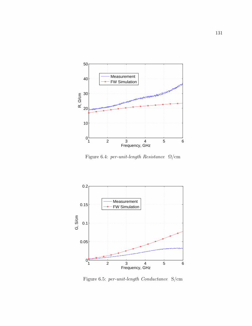
131
1 2 3 4 5 60
10
20
30
40
50
Frequency, GHz
R, Ω
/cm
MeasurementFW Simulation
Figure 6.4: per-unit-length Resistance Ω/cm
1 2 3 4 5 60
0.05
0.1
0.15
0.2
Frequency, GHz
G, S
/cm
MeasurementFW Simulation
Figure 6.5: per-unit-length Conductance S/cm

132
1 2 3 4 5 60
10
20
30
40
50
Frequency, GHz
Zc
Mod
ule,
ΩMeasurementFW Simulation
Figure 6.6: Module of the Characteristic Impedance Zc
1 2 3 4 5 6−60
−40
−20
0
20
40
60
Frequency, GHz
Zc
Ang
le, Ω
MeasurementFW Simulation
Figure 6.7: Phase of the Characteristic Impedance Zc
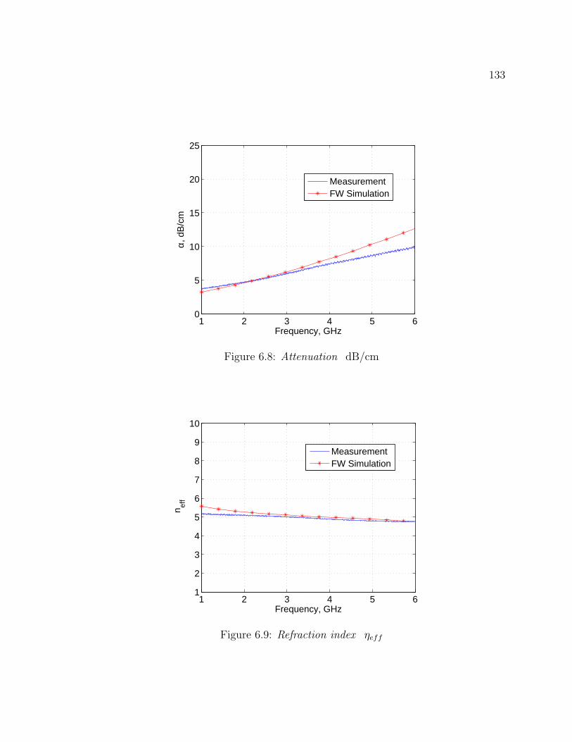
133
1 2 3 4 5 60
5
10
15
20
25
Frequency, GHz
α, d
B/c
mMeasurementFW Simulation
Figure 6.8: Attenuation dB/cm
1 2 3 4 5 61
2
3
4
5
6
7
8
9
10
Frequency, GHz
nef
f
MeasurementFW Simulation
Figure 6.9: Refraction index ηeff

134
6.3 MTL characterization methods
Various parameter extraction techniques for MTL structures were studied and valu-
ated. A brief discussion follows and finally an example in which an accurate technique
without optimization [38] is implemented will be presented.
Groudis and Chang [23] have previously developed a frequency domain method
to extract parameter matrices R, L, C and G from the two-port impedance Z and
admittance Y matrices. This method is based on a combination of the method of
characteristics and the decoupled mode transformation in frequency domain. In this
procedure, the solution of the MTL equations (2.3.12) and (2.3.13) is assumed as
follows:
V = A.exp(−Γz) + B · exp(Γz) (6.3.1)
Y−1C I = A.exp(−Γz)−B.exp(Γz) (6.3.2)
where
Γ = (ZY)1/2 = PγP−1 (6.3.3)
YC = Z−1Γ = YΓ−1 (6.3.4)
P is the eigenvector matrix of Γ. It is also the eigenvector matrix of the ZY prod-
uct, being γ the diagonal eigenvalue matrix of Γ. Applying properties the following
relationship is derived:
exp(−Γz) = Pexp(−γz)P−1 (6.3.5)

135
In the solution it is assumed that the matrix Γ = (ZY)−1 exists and that the
characteristic admittance matrix YC is symmetrical. Following the reasonings given
in [41], a MTL with n+1 conductors of length d can be treated as a 2n-port network,
having n ports on the input end (subindex i) and n ports on the output end (subindex
o). Then, it can be proven [7] that:
[Ii
Io
]=
[YC cothΓd −YC sinh−1 Γd
−YC sinh−1 Γd YC cothΓd
]·[
Vi
Vo
](6.3.6)
with a short-circuit admittance matrix Y2n of the 2n-port network given as:
Y2n =
[YA YB
YB YA
](6.3.7)
where
YA = YC cothΓd
YB = −YC sinh−1 Γd(6.3.8)
and
cothΓd = P(coth γd)P−1
sinh−1 Γd = P(sinh−1 γd)P−1(6.3.9)
And, the open-circuit impedance matrix Z2n is given by:
Z2n =
[ZA ZB
ZB ZA
](6.3.10)
where
ZA = (cothΓd)Y−1C
ZB = (sinh−1 Γd)Y−1C
(6.3.11)
136
Two methods to derive the YC and Γ matrices were proposed in [23]. The first one
is to be used when the transmission line attenuation is small, and it is not interesting
for lossy lines.
The second method is to be used with high attenuation or lossy lines. This case
may occur either because the line is sufficiently long, or because the frequency of
interest is so high that losses due to skin effect and proximity effect are significant.
It involves measurements at both input and output ends of the MTLs.
A brief discussion of this method is provided in the following. From equation
(6.3.7) we have:
−Y−1B YA = coshΓd (6.3.12)
Γd = P(cosh−1 Λ)P−1 (6.3.13)
where P is the eigenvector matrix of Γd and −Y−1B YA. Equations (6.3.3) and
(6.3.13) give:
γd = cosh−1 Λ (6.3.14)
and from (6.3.7) and (6.3.13) the characteristic admittance matrix YC is found
to be:
YC = −YB sinhΓd
= −YBP[sinh(cosh−1 Λ)]P−1(6.3.15)
This, from (6.3.14) the per-unit-length modal attenuation constant αm and per-
unit-length modal phase constant βm are obtained by dividing the real and the imag-
inary parts by d and ωd respectively.

137
Then, the per-unit-length parameters R, L, C and G can be derived by replacing
and equating into (6.3.4) the results Γ and YC respectively obtained from (6.3.13)
and (6.3.16), as follows:
Z = R + jωL = ΓY−1C
Y = G + jωC = YCΓ(6.3.16)
This method was tested by using a Full Wave EM simulation2 on a 4-Ports asym-
metric microstrip line and it was found not to achieve symmetry for the above per-
unit-length parameters R, L, C and G and to produce results without physical
meaning. Reasons for this are that the procedure presupposes symmetries for Z and
Y up to frequencies under the Ghz region, in which their authors have validated it.
As was explained in last chapters, these symmetries are intended to be broken in high
lossy media, as in high frequency, this the procedure needs to be modified to take
asymmetries into account.
A great limitation of the method is that it needs to be optimized by a proper
algorithm. Another drawback is that the convergency bandwidth is limited by the
heuristic rule of thumb `MTL ≤ λ/10, where `MTL is the MTL length in the prop-
agation direction and λ is the wavelength of the EM wave propagating along the
structure.
Another methodology was developed by Knockaert et al [29] to recover lossy MTL
parameters from Scattering matrix. The method is based on a generalization of the
simultaneous diagonalization technique by means of congruence transformations to
the general lossy reciprocal case.
2Simulation was made with the EM simulator EMSight of AWR, that includes a fast Full Waveelectromagnetic solver based in a modified Spectral-domain method of moments.
138
This procedure is based on the symmetry and reciprocity properties of the Z and
Y matrices, and the solution is obtained through the chain parameter matrix Φ(z)
defined in equations (2.3.16) and (2.3.17), that is rewritten as:
Φ(z) = exp
− z
(0 Z
Y 0
)=
[Ω α
β ΩT
]
=
[φ1
(z2ZY
) −zZφ2
(z2ZY
)
−zYφ2
(z2ZY
)φ1
(z2ZY
)] (6.3.17)
where the superscript T indicates Hermitian adjoint matrix (conjugate transpose)
and the entire functions φ1(z) and φ2(z) are defined as:
φ1(z) = cosh(√
z)
φ2(z) = sinh(√
z)/√
z(6.3.18)
Noting that α and β are symmetric, also Ωα and βΩ are symmetric. The authors
of [29] assume that Ω2 = In + αβ (with In is the n× n identity matrix) and that the
following relation needs to be achieved:
[Ω α
β ΩT
]·[
Ω −α
−β ΩT
]=
[In 0
0 In
]= I2n (6.3.19)
With this assumptions, the 2n× 2n Z2n-matrix description of a MTL is given by:
[Vi
Vo
]=
[Z2n
] ·[
Ii
Io
](6.3.20)

139
and based on the symmetry assumption:
Z2n =
[A B
B A
]=
[−β−1ΩT −β−1
α− Ωβ−1ΩT −β−1Ω−1
](6.3.21)
where A and B are symmetric n× n matrices. These relationships follow:
β = −B−1, Ω = AB−1, α = B − AB−1A (6.3.22)
With the matrices A and B given from the Z2n-matrix description, the Z and Y
matrices are recovered from the equations:
AB−1 = φ1
(z2ZY
)
B−1 = −zYφ2
(z2ZY
) (6.3.23)
By assuming that the eigenvalues of AB−1 and ZY are all distinct, the resulting
decompositions are given as:
AB−1 = PδzP−1, ZY = PδtP
−1 (6.3.24)
and the related simultaneous congruence decompositions given by
A = PδaPT , B = PδbP
T , Z = PδrPT , Y = P−T δgP
−1 (6.3.25)
Using the above relationships, the following equations for the δ(·) diagonal matrices
were derived [29]:
δaδ−1b = δz
δrδg = δt
δz = φ1(z2δt)
δ−1b = zδgφ2(z
2δt)
(6.3.26)

140
From the above equations, the MTL parameters can be obtained from the Z2n-
matrix. The following general formula is derived:
δt =1
z2[arg cosh(δz) + j2πδn]2 (6.3.27)
where δn is a diagonal matrix with integer entries that takes into account the
multiple branches of the inverse function of φ1(z) = cosh(√
z).
This algorithm intends to solve (6.3.27) specifying an index vector of integers, the
entries of the diagonal matrix δn, in order to retrieve the correct MTL parameters. It
has a direct connection with the MTL length z, since the method tries to find T from
a matrix exponential exp(zT). For the scalar case this creates phase related problems
to be solved to obtain an estimate for λ, given t = eλz. Approximations for this scalar
case are generalized to the matrix exponential and a general solution, that includes
the generation of the index vectors, was developed in [29].
The author of the present work has tested the mentioned algorithm in a 4-Ports
asymmetric microstrip line simulated with a Full Wave EM simulation3. Limitations
due to convergency problems were encountered in solving (6.3.27), where a difficulty
to reach diagonal matrices needs to be optimized in the original algorithm. In this
procedure, symmetries for Z and Y matrices were assumed, thus high lossy MTL
structures are not properly characterized.
Other approaches are proposed in the literature [25][38][48][49]. The procedure
presented by Arz et al [48] uses statistical measurement methodology based on Marks
algorithm [35] as an enhancement of the TRL algorithm.
3Simulation was made with the EM Full Wave simulator EMSight of AWR.

141
In the present work a procedure that doesn’t require optimization [37][38] and
that gives accurate results was implemented. A discussion of the method, examples
of characterization and limitations are given in the following paragraphs.

142
6.3.1 MTL parameters extraction from S-Matrix
A method for extracting the circuit models for MTLs from black-box parameters
was developed by Martens and Sercu [38]. If the number of conductors in a MTL is
large, the model will have many parameters to be extracted and non physical values
may be obtained or the extraction process does not converge as was seen in previous
paragraphs. Simultaneous optimization requires great computational effort and needs
error estimation routines.
The direct extraction method without optimization is valid for small MTL lengths
compared with wavelengths of propagating waves. If T or Π circuit models are pro-
posed, a direct relation is found between the Z and Y matrices and the circuit
parameters.
A brief explanation is given: an MTL with 2n access ports is considered, then if
two RL sections and one GC section (T-circuit model) or two GC sections and one RL
section (Π-circuit model) are sufficient to obtain an accurate model, no optimization
process is needed to determine the parameter values of the model [38]. They can be
directly calculated from the black-box Scattering parameters.
We consider a (n+1) conductors MTL, the 2n×2n S-matrix consists in four n×n
submatrices as follows [25]:
S =
[Sin,in Sin,out
Sout,in Sout,out
](6.3.28)
Then, we can find the impedance Z2n and admittance Y2n matrices from the

143
Scattering matrix as:
Z2n = Zref · [I+ S][I− S]−1
Y2n = Z−1ref · [I− S][I+ S]
(6.3.29)
where I is the 2n×2n identity matrix. To obtain the parameter values the 2n×2n
Z2n and Y2n are defined as:
Z2n =
[Zin,in Zin,out
Zout,in Zout,out
]and Y2n =
[Yin,in Yin,out
Yout,in Yout,out
](6.3.30)
Then the per-unit-length parameters R, L, C and G of the T-circuit model, as
shown in Fig. 6.10, are related to the above matrices as follows:
R(1) = <(Zin,in − Zin,out)
L(1) = =(Zin,in − Zin,out)/ω
C = =(Z−1in,out)/ω
G = <(Zin,out)
R(2) = <(Zout,out − Zin,out)
L(2) = =(Zout,out − Zin,out)/ω
for T circuit (6.3.31)
where the supraindex (1) indicates the input RL branch of the T-circuit model and
the supraindex (2) indicates the output T-circuit model RL branch.

144
Figure 6.10: MTL T-circuit model
In an analogue way, the per-unit-length parameters R, L, C and G of the Π-circuit
model, as shown in Fig. 6.11, can be found from the following relationships:
G(1) = <(Yin,in + Yout,in)
C(1) = =(Yin,in + Yout,in)/ω
R = <(−Y−1out,in)
L = =(−Y−1out,in)/ω
G(2) = <(Yout,out + Yout,in)
C(2) = =(Yout,out + Yout,in)/ω
for Π circuit (6.3.32)
where the supraindex (1) indicates the input GC branch of the Π-circuit model
and the supraindex (2) indicates the output Π-circuit model GC branch.
Although this methodology was originally developed for small high-speed IC inter-
connections, it was proven to work very well for MTLs with lengths `MTL ≤ λmin/20
being λmin the wavelength for the maximum frequency propagated along the line.

145
Figure 6.11: MTL Π-circuit model
The major advantage of the direct calculation method is that a very accurate
model is obtained quickly. A disadvantage is that the model is only valid for lengths
that are small with respect to the wavelength.
In the next paragraphs the experimental results of a simulation and characteri-
zation of a 4-Ports asymmetric coupled microstrip line structure using the present
methodology will be discussed.

146
6.3.2 MTL simulation and experimental results
A 4-Port asymmetric coupled microstrip line structure was tested through the method
discussed in the last section. It was assumed that the signal paths are connected
from the ground plane to the signal conductors, and coupled modes are intended to
be propagated through the line.
A geometry of the structure with length `MTL = 1 mm is shown in Fig. 6.12
where the 30 µm wide signal conductor on the left is separated from the 200 µm wide
signal conductor on the right by a 50 µm wide gap. The 100 µm thick substrate has
a relative dielectric constant of 12.9. The 0.5 µm thick signal conductors and 5 µm
thick ground plane have a conductivity σ = 3.602× 10⁷ S/m.
Figure 6.12: Asymmetric Coupled Microstrip Line
A Full Wave EM simulation of the structure’s behavior was performed by using the
MWOffice c© EM simulator of AWRr, based on the modified Spectral-domain method
of moments in a range of frequency from DC to 5 Ghz. Through the S-matrix the
above characterization method [38] was used to extract the circuit parameters and
the following results were obtained:

147
1 2 3 4 50
5
10
15
20
Frequency, GHz
R, Ω
/cm
R11
R22
R12
R21
Figure 6.13: per-unit-length R(f) Ω/cm matrix
1 2 3 4 50
1
2
3
4
5
6
7
8
Frequency, GHz
L, n
Hy/
cm
L11
L22
L12
L21
Figure 6.14: per-unit-length L(f) nHy/cm matrix

148
1 2 3 4 50
0.5
1
1.5
2
2.5
Frequency, GHz
C, p
F/c
m C
11
C22
−C12
−C21
Figure 6.15: per-unit-length C(f) pF/cm matrix
As can be seen the skin effect influences the R matrix values as is evident from
Fig. 6.13. A frequency dependent behavior or the L matrix values is observed and
can be seen in graphic Fig. 6.14.
In the graphic of Fig. 6.15, the C matrix values are plotted with a quasi constant
behavior the along frequency bandwidth. A similar experiment was presented in [8]
and compared with our results, giving a very good agreement between them. This
fact evidences the power of the characterization methodology proposed and tested,
as it is compared with other different approaches.
On the other hand, the diagonal matrices modal attenuations [α] and the modal
refractive indices [ηeff ] were extracted by equating the formula (6.3.3) as follows:
[α] = <(Γ), and [ηeff ] = c[β]
ω(6.3.33)
giving the results shown in figures 6.16 and 6.17:
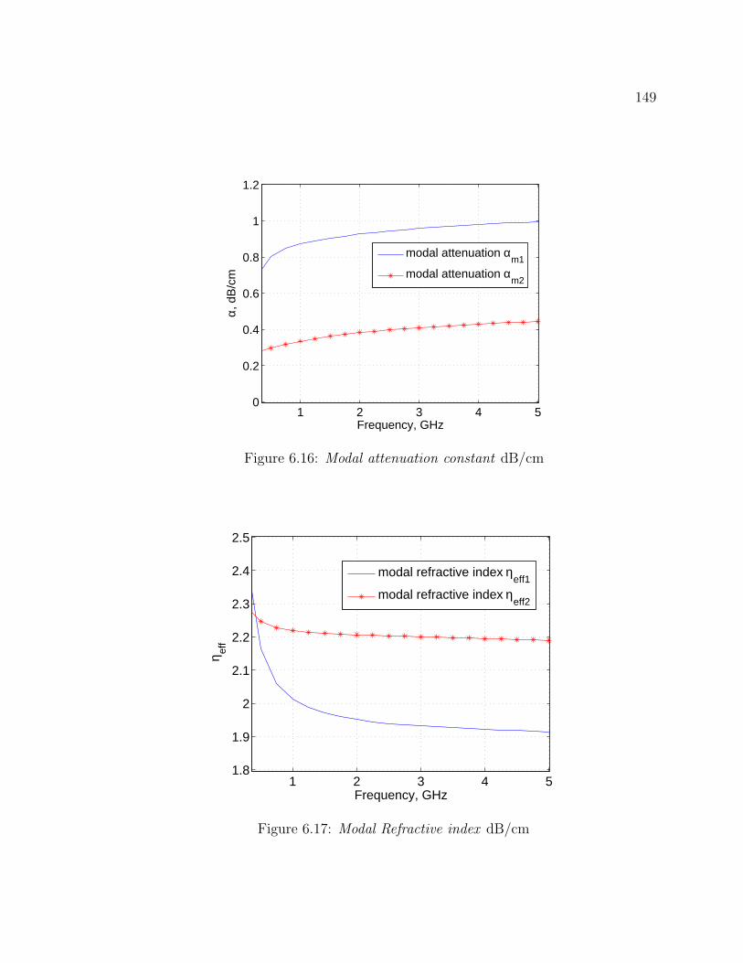
149
1 2 3 4 50
0.2
0.4
0.6
0.8
1
1.2
Frequency, GHz
α, d
B/c
m
modal attenuation αm1
modal attenuation αm2
Figure 6.16: Modal attenuation constant dB/cm
1 2 3 4 51.8
1.9
2
2.1
2.2
2.3
2.4
2.5
Frequency, GHz
ηef
f
modal refractive index ηeff1
modal refractive index ηeff2
Figure 6.17: Modal Refractive index dB/cm

150
Finally, the influence of the modal cross powers for coupled modes along the struc-
ture was validated by calculating the ζnm merit coefficient index [50] from the ex-
tracted Z and Y matrices. As can be seen from Fig. 6.18, a small 1.5 % influence
of the modal cross powers is noted near DC frequency values.
0 1 2 3 4 50
0.5
1
1.5
2
Frequency, GHz
ζ mn (
%)
Figure 6.18: Modal Cross Power ζnm merit coefficient index

Chapter 7
Conclusions
7.1 Summary
As stated in the Introduction, the present work was conceived as a framework of ideas
focused on a methodology for characterizing high frequency waveguides on silicon
substrates.
A general methodology for RF lossy lines characterization was implemented and
tested. This methodology is based on the transmission line theory and on heuristic
assumptions that take care of deviations for the classical model.
To achieve realistic results it was necessary to explore the limitations of the Teleg-
rapher’s equation in order to understand the important phenomena at high frequency.
Accurate models and suitable parameters were analyzed and presented. A large part
the information in the present work derives from a large number of sources and a
particular effort was made to organize it into a coherent framework of tools for this
particular field of knowledge.
A quantification of the classical model deviation is presented as a starting point
for the development of further models.
151

152
A fully automated VNA driver under MATLAB environment has been developed
and used to do experimental measurements. Different measurements cases were stud-
ied, compared and used.
Particular attention was given on the TRL calibration technique as the more
suitable technique for waveguide and transmission line characterization.
Different measurements were made with the automated measurement tool devel-
oped ad hoc for the present work. Good agreement with theoretical behaviors of
coaxial media have proven the correct functionality of this setup.
Different methods to extract useful electrical pul parameters of transmission lines
from scattering matrix were explored, studied and compared. An extraction proce-
dure for single lossy lines has been tested by using experimental measurement on
silicon substrate lines. Good agreement was found with full wave simulations as
theoretical reference, giving a confirmation of the correctness of the characterization
methodology adopted.
Accurate models and extraction procedures of multi-conductor transmission lines
were tested and compared with the selected literature results. Also in this case there
has been a good agreement between the results obtained by the proposed approach
and the published ones.

153
7.2 Future works
The extension of the MTL extraction technique using experimental data requires the
implementation of a multiport calibration technique.
Different ways for the optimization of MTL characterization methods for lossy
lines accounting for topology asymmetries need to be explored.
The development of a general model with parameters that take into account the
effects of coupled modes in MTL is referred in the present work and even if its validity
has to be experimentally addressed.

The reward of a thing well done is to have done it.
Ralph Waldo Emerson
154

Out of Context... ?
What is truth?
As a question out of context it seems a pretext for a possible answer.
The truth, intended as a knowledge who has a particular meaning for our brain;
is based on the interpretation of the reality through experience and it needs to be
revised in case of misinterpretation.
Interpretation of the facts of Nature, the phenomena, is the aim of modern science,
where the method of inquiring is the most important thing to be solved.
As a dialogue between man and nature, the inquiring predisposes to the answers...
From Galileo to the Information Age; the question was the ”nature of things and
its relationships”, where the method of interpretation was the key for the construction
of knowledge.
After the consequences on the nature by the arbitrary use of the method of in-
quiring, and after all the knowledge, the following questions need to be answered:
It is possible to change the method of inquiring?
How to do with the knowledge?.
Technologies, can only answer the question of the efficient use of ”knowledge”.
Then, the ”sense of the use of the knowledge” needs to be answered.
A philosophical answer for the sense of the use of the knowledge can be The Truth,
intended as a relationship between man and nature.
Science needs to ask itself some philosophical question... as for example: which
are the ultimate scopes and attitudes who command this relationship?
The whole dialogue implicates a relationship, then, a sense can be defined into the
context of a relationship, but the sense for a relationship is the relationship itself!
The author’s experience taught him that the ultimate sense of knowledge is Love,
intended as a relationship; then, as a consequence, he believes that empirically :
155

156
The Truth is in the Truth
Love is Truth

Appendix A
See User’s Guide Draft Version attached
157

Bibliography
[1] U. Ravaioli A. Cangellaris, J. Schutt-Aine and A. Deutsch, Interactive Tuto-
rial on Fundamentals of Signal Integrity for High-Speed/High-Density Design,
SEMCHIP, ECE Dept. University of Illinois, Urbana-Champaign, T.J Watson
Research Center,IBM Corporation, 2001.
[2] Ramachandra Achar and Michel S. Nakhla, Simulation of High-Speed Intercon-
nects, Proceedings of the IEEE Vol 89 (2001), 693–728.
[3] F. Amantione and S. Pensa, Progetto e misura di strutture a microonde per
componenti fotonici ad alta frequenza, Tesi di Laurea, Politecnico di Torino,
Torino, Italy, 2000.
[4] S. Ridella B. Bianco, M. Parodi and F. Selvaggi, Launcher and microstrip char-
acterization, IEEE Transactions on Instrumentation and Measurements Vol 25
(1987), no. 4, 320–323.
[5] J. R. Brews, Transmission line models for lossy waveguide interconnections in
VLSI, IEEE Transactions on Electronic Devices (1986), 1356–1365.
[6] , Characteristic Impedance of Microstrip Lines, IEEE Transactions on
Microwaves Theory and Techniques Vol 35 (1987), no. 1, 30–34.
[7] Robert E. Collin, Foundations for Microwave Engineering, McGraw Hill, New
York, 1992.
158

159
[8] L. Hayden D. Williams and R. Marks, A Complete Multimode Equivalent Circuit
Theory for Electrical Design, Journal of Research of the NIST Vol 102 (1997),
no. 4, 405–423.
[9] W. R. Eisenstadt and Y. Eo, S-Parameter-Based IC Interconnect Transmission
Line Characterization, IEEE Transactions on Components, Hybrids, and Manu-
facturing Technology Vol 15 (1992), no. 4, 483–490.
[10] , High-Speed VLSI Interconnect Modelling Based on s-Parameter Mea-
surements, IEEE Transactions on Components, Hybrids, and Manufacturing
Technology Vol 16 (1993), no. 5, 555–562.
[11] G. Engen and C. Hoer, Thru-Reflect-Line: An Improved Technique for Cali-
brating the Dual Six Port Automatic Network Analyzer, IEEE Transactions on
Microwaves Theory and Techniques Vol 27 (1979), no. 12, 987–993.
[12] A. Deutsch et al, When are Transmission-Line Effects Important for On-Chip
Interconnections?, IEEE Transactions on Microwaves Theory and Techniques
Vol 45 (1997), no. 10, 1836–1846.
[13] H.J. Eul and B. Schiek, Thru-Reflect-Match: One Result of a Rigorous Theory
for Deembedding and Network Analyzer Calibration, Proceedings of European
Microwave Conference, Stockolm (1987), 909–914.
[14] G. Ghione F. Bertazzi and M. Goano, Efficient Quasi-TEM Frequency-
Dependent Analysis of Lossy Multiconductor Lines Through a Fast Reduced-
Order FEM Model, IEEE Transactions on Microwaves Theory and Techniques
Vol 51 (2003), no. 9, 2029–2035.

160
[15] M. Goano G. Ghione R. Orta F. Bertazzi, O. A. Peverini and R. Tascone, A
Fast Reduced-Order Model for the Full-Wave FEM Analysis of Lossy Inhomo-
geneous Anisotropic Waveguides, IEEE Transactions on Microwaves Theory and
Techniques Vol 50 (2002), no. 9, 2108–2114.
[16] D. De Zutter F. Olyslager and A. T. de Hoop, New reciprocal circuit model for
lossy waveguide structures based on the orthogonality of the eignemodes, IEEE
Transactions on Microwaves Theory and Techniques Vol 42 (1994), no. 12, 2261–
2269.
[17] N. Fachee and D. De Zutter, New High-Frequency Circuit Model for Coupled
Losses and Lossy Waveguide Structures, IEEE Transactions on Microwaves The-
ory and Techniques Vol 27 (1990), no. 12, 252–259.
[18] A. Ferrero and U. Pisani, QSOLT: A new fast algorithm for two port S parameter
measurements, 38th ARFTG Conference Digest, San Diego, California. (1991),
505–507.
[19] , Two-port network analyzer calibration using and unknown thru, IEEE
Microwave and Guided Wave Letters Vol 2 (1992), 505–507.
[20] Andrea Ferrero, Caratterizzazione di dispositivi attivi a microonde in regime di
liearita e non linearita, Tesi di Dottorato, Politecnico di Torino, Torino, Italy,
1992.
[21] I. Maio G. Ghione and G. Vecchi, Modelling of Multiconductor Buses and Anal-
ysis of Crosstalk, Propagation Delay, and Pulse Distortion in High-Speed GaAs
Circuits, IEEE Transactions on Microwaves Theory and Techniques Vol 37
(1989), no. 3, 445–456.
[22] G. Ghione and M. Pirola, Elettronica delle Microonde, Otto Editore, Torino,
2002.

161
[23] A. J. Groudis and C. S. Chang, Coupled Lossy Transmission Line Characteriza-
tion and Simulation, IBM Journal of Research and Development Vol 25 (1981),
no. 1, 25–41.
[24] M. Furukawa H. Hasegawa and H. Yanai, Properties of Microstrip Line on Si-
SiO2 System, IEEE Transactions on Microwaves Theory and Techniques Vol 19
(1971), no. 11, 869–881.
[25] D. Trainor J. Nickel and J. Schutt-Aine, Frequency-Domain-Coupled Microstrip-
Line Normal-Mode Parameter Extraction from S-Parameters, IEEE Transactions
on Electromagnetic Compatibility Vol 43 (2001), no. 4, 495–503.
[26] M. B. Steer J. S. Kasten and R. Pomwerleu, Enhanced Through-Reflect-Line
Characterizations of Two-Port Measureing Systems Using Free-Space Capaci-
tance Calculation, IEEE Transactions on Microwaves Theory and Techniques
Vol 38 (1990), no. 2, 215–217.
[27] R. Grag K. C. Gupta and R. Chada, Computer Aided Design of Microwave
Circuits, Artech House, Dedham MA, USA, 1981.
[28] K. Kurokawa, Power Waves and the Scattering Matrix, IEEE Transactions on
Microwaves Theory and Techniques Vol 19 (1965), no. 11, 194–202.
[29] F. Olyslager E. Laermans L. Knockaert, D. De Zutter and J. De Geest, Recov-
ering Lossy Multiconductor Transmission Line Parameters from Impedance or
Scattering Representations, IEEE Transactions on Advanced Packaging Vol 25
(2002), no. 2, 200–205.
[30] G. Madonna and K. Kerwin, Network Analyzer Calibration Techniques, Agilent
Technologies,Microwave Technology Division - Politecnico di Torino, Santa Rosa
CA, USA, 1999.

162
[31] R. Marks and D. Williams, The Interpretation and use of S-parameters in Lossy
Lines, 38th ARFTG Conference Digest, Monterrey, California. (1990), 84–90.
[32] , Characteristic Impedance Determination Using Propagation Constant
Measurement, IEEE Microwave and Guided Wave Letters Vol 1 (1991), no. 6,
141–143.
[33] , Transmission Line Capacitance Measurement, IEEE Microwave and
Guided Wave Letters Vol 1 (1991), no. 9, 243–145.
[34] , A General Waveguide Circuit Theory, Journal of Research of the NIST
Vol 97 (1992), no. 5, 533–562.
[35] Roger B. Marks, A Multiline Method of Network Analyzer Calibration, IEEE
Transactions on Microwaves Theory and Techniques Vol 39 (1991), 1205–1215.
[36] , Formulation of the Basic Network Analyzer Error Model including
Switch Terms, 50 Automatic RF Techniques Group Confefence (1997), 505–507.
[37] L. Martens and S. Sercu, Characterizing N-port packages and interconnections
with a 2-port network analyzer, IEEE 6th Topical Meeting on Electrical Perfor-
mance of Electronic Packaging (1997), 163–167.
[38] , Parameter Extraction for Circuit Models of Electronic Packages without
optimization, IEEE 8th Topical Meeting on Electrical Performance of Electronic
Packaging (1999), 71–74.
[39] K. D. Marx, Propagation modes, equivalent circuits, and characteristic termi-
nations for multiconductor transmission lines with inhomogeneous dielectrics,
IEEE Transactions on Microwaves Theory and Techniques Vol 21 (1973), no. 7,
450–457.
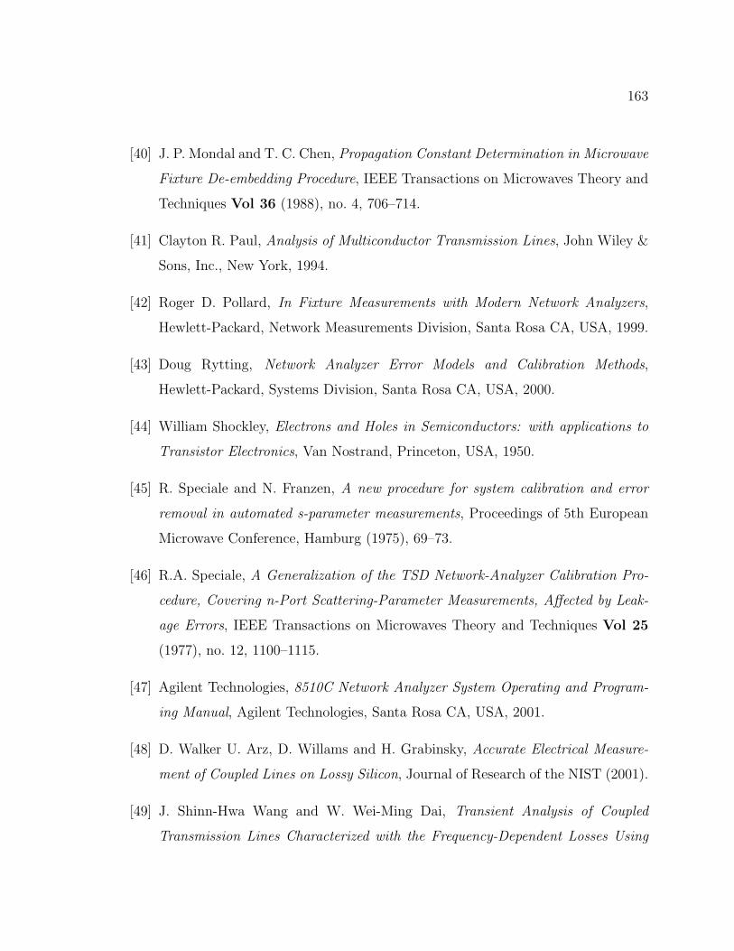
163
[40] J. P. Mondal and T. C. Chen, Propagation Constant Determination in Microwave
Fixture De-embedding Procedure, IEEE Transactions on Microwaves Theory and
Techniques Vol 36 (1988), no. 4, 706–714.
[41] Clayton R. Paul, Analysis of Multiconductor Transmission Lines, John Wiley &
Sons, Inc., New York, 1994.
[42] Roger D. Pollard, In Fixture Measurements with Modern Network Analyzers,
Hewlett-Packard, Network Measurements Division, Santa Rosa CA, USA, 1999.
[43] Doug Rytting, Network Analyzer Error Models and Calibration Methods,
Hewlett-Packard, Systems Division, Santa Rosa CA, USA, 2000.
[44] William Shockley, Electrons and Holes in Semiconductors: with applications to
Transistor Electronics, Van Nostrand, Princeton, USA, 1950.
[45] R. Speciale and N. Franzen, A new procedure for system calibration and error
removal in automated s-parameter measurements, Proceedings of 5th European
Microwave Conference, Hamburg (1975), 69–73.
[46] R.A. Speciale, A Generalization of the TSD Network-Analyzer Calibration Pro-
cedure, Covering n-Port Scattering-Parameter Measurements, Affected by Leak-
age Errors, IEEE Transactions on Microwaves Theory and Techniques Vol 25
(1977), no. 12, 1100–1115.
[47] Agilent Technologies, 8510C Network Analyzer System Operating and Program-
ing Manual, Agilent Technologies, Santa Rosa CA, USA, 2001.
[48] D. Walker U. Arz, D. Willams and H. Grabinsky, Accurate Electrical Measure-
ment of Coupled Lines on Lossy Silicon, Journal of Research of the NIST (2001).
[49] J. Shinn-Hwa Wang and W. Wei-Ming Dai, Transient Analysis of Coupled
Transmission Lines Characterized with the Frequency-Dependent Losses Using

164
Scattering-Parameter Based Macromodel, Baskin Center, University of Califor-
nia, Santa Cruz CA, USA, March 1995.
[50] D. Williams and F. Olyslager, Modal cross power in quasi-TEM transmission
lines, IEEE Microwave and Guided Wave Letters Vol 6 (1996), no. 11, 413–415.
[51] Dylan F. Williams, Thermal Noise in Lossy Waveguides, IEEE Transactions on
Microwaves Theory and Techniques Vol 44 (1996), no. 7, 1067–1073.