Wafer Prober Plug-in for Test Automation · software. Test steps realize wafer chuck movement and...
15
Find us at www.keysight.com Page 1 Wafer Prober Plug-in for Test Automation on PathWave Workflow Automation for Silicon Photonics Wafer Probing The Keysight Test Automation on PathWave (TAP) software provides powerful, flexible and extensible test sequence and test plan creation with additional capabilities that optimize your test software development and overall performance. The Wafer Prober Plug-in supports your workflow automation for integrated and Silicon Photonics wafer probing and test. Keysight TAP is a modern Microsoft .NET-based application that can be used stand-alone or in combination with higher-level test executive software environments. Leveraging C# and the power of Microsoft Visual Studio, TAP is not just another programming language. It’s a platform upon which you can build your test solutions, maximizing your team’s productivity by using your existing software development tools and infrastructure.
Transcript of Wafer Prober Plug-in for Test Automation · software. Test steps realize wafer chuck movement and...
P
a
g
e
Find us at www.keysight.com Page 1
Wafer Prober Plug-in for Test
Automation on PathWave
Workflow Automation for Silicon Photonics Wafer Probing
The Keysight Test Automation on PathWave (TAP) software provides powerful, flexible and
extensible test sequence and test plan creation with additional capabilities that optimize your
test software development and overall performance. The Wafer Prober Plug-in supports
your workflow automation for integrated and Silicon Photonics wafer probing and test.
Keysight TAP is a modern Microsoft .NET-based application that can be used stand-alone or
in combination with higher-level test executive software environments. Leveraging C# and
the power of Microsoft Visual Studio, TAP is not just another programming language. It’s a
platform upon which you can build your test solutions, maximizing your team’s productivity
by using your existing software development tools and infrastructure.
P
a
g
e
Find us at www.keysight.com Page 2
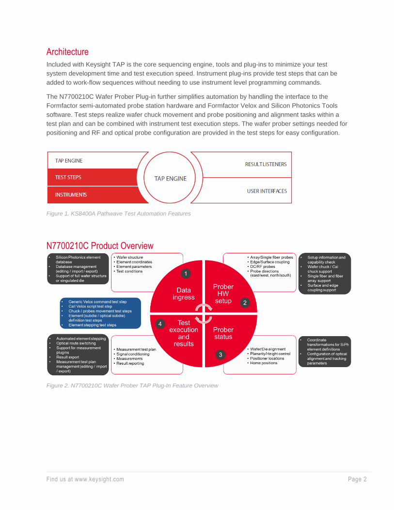
Architecture
Included with Keysight TAP is the core sequencing engine, tools and plug-ins to minimize your test
system development time and test execution speed. Instrument plug-ins provide test steps that can be
added to work-flow sequences without needing to use instrument level programming commands.
The N7700210C Wafer Prober Plug-in further simplifies automation by handling the interface to the
Formfactor semi-automated probe station hardware and Formfactor Velox and Silicon Photonics Tools
software. Test steps realize wafer chuck movement and probe positioning and alignment tasks within a
test plan and can be combined with instrument test execution steps. The wafer prober settings needed for
positioning and RF and optical probe configuration are provided in the test steps for easy configuration.
Figure 1. KS8400A Pathwave Test Automation Features
N7700210C Product Overview
Figure 2. N7700210C Wafer Prober TAP Plug-In Feature Overview

P
a
g
e
Find us at www.keysight.com Page 3
Features
The Keysight Wafer Prober TAP Plug-In supports integrated photonics test workflow for
both wafer and singularized die testing by:
1. Data ingress for wafer structure, device coordinates, device parameters and test conditions based on
.csv and .xml files
2. Prober hardware setup for configuring the probe station for array & single fiber probes, edge &
surface coupling, RF & DC electrical probes and probe orientations
3. Test steps that combine common probe station commands for prober and probe control and prober
status inquiry
4. Communication to probe station and to other instrument plug-ins for test execution, test set-up and
instrument conditioning, and result management
The N7700210C Wafer Prober TAP Plug-in simplifies automation by providing easy-to-use measurement
steps for the Formfactor probe station that handle all the details for configuring the CM300xi silicon
photonics probe station and Formfactor Velox and Silicon Photonics Tools software.
Operation
An example test setup for integrated photonics is shown below:
Figure 3. Example Test Setup for Optical and Electro-optical DC & RF Test
P
a
g
e
Find us at www.keysight.com Page 4
Tunable Lasers, Lightwave Component Analyzer and Optical Power Meters are connected to the device
input and output ports via polarization synthesizers and optical switches. The optical switches route the
optical test signals to and from different ports of the fiber array the test instruments. The detector
connected to the LogAmp serves for the active alignment of the optical fibers to the device under test
(DUT). RF and DC probes connect to the electrical ports of the integrated photonics device.
An integrated photonics test plan typically consists of a combination of test execution steps for:
• Controlling the probe station for moving the wafer chuck and the optical and electrical probes to the
device to be tested on the wafer or die.
• Configuring signal routes between the instruments and the optical and electrical probes to device I/O
ports.
• Performing measurements by first stepping the wafer and probes to the device IO ports, performing
automated alignment for optimum coupling and then triggering a measurement.
• Measurement steps automatically pull geometric and position information about the optical and
electrical device ports on wafer or die from the wafer and device data base and the corresponding
test conditions from the measurement plan.
Configuring the workflow with sequences of steps and coordination with other instruments and
resources using TAP is a powerful contribution to enhancing efficiency in test development and
throughput.
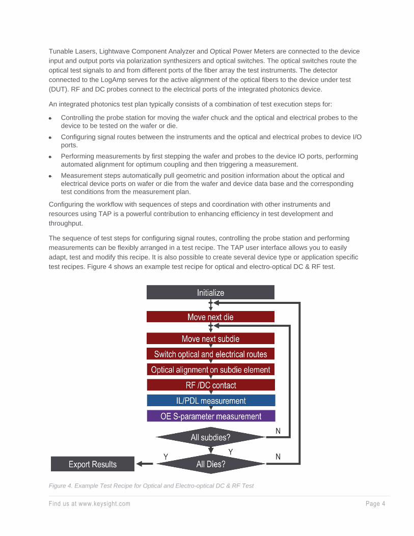
The sequence of test steps for configuring signal routes, controlling the probe station and performing
measurements can be flexibly arranged in a test recipe. The TAP user interface allows you to easily
adapt, test and modify this recipe. It is also possible to create several device type or application specific
test recipes. Figure 4 shows an example test recipe for optical and electro-optical DC & RF test.
Figure 4. Example Test Recipe for Optical and Electro-optical DC & RF Test
P
a
g
e
Find us at www.keysight.com Page 5
This test recipe is realized by a test plan in the TAP software as described in chapter “Measurement
Steps and Test Plan”. Test plans can be generated independent of individual wafers. The above example
in Figure 4 would serve wafers with CWDM receivers where detector structures are coupled to drop filters
that would need wavelength dependent responsivity measurements over an optical channel window and
an opto-electrical S-parameter measurement at the channel center wavelength. In a Measurement Plan
the user can select which devices will be tested for a particular wafer. In the measurement plan the user
can also specify several different measurements on a particular element, like bandwidth measurement
under different detector bias conditions. Each measurement has an individual measurement ID that is
used by the measurement steps for saving measurement results.
Installation
The details needed to install and use the TAP software are given in the plug-in help file. Briefly this entails
the following steps.
• Installing Formfactor Velox and SiPh-Tools SW on the measurement PC
• Downloading and installing TAP (KS8400A) and the wafer prober plug-in (N7700210C)
• Optionally installing other SW and plug-ins like N7700100C Photonic Application Suite incl. TAP plug-
in, N4370P01A (LCA plug-in) or KS8105A (Switch Manager)
• Installing the purchased or temporary evaluation TAP licenses.
• Then starting Velox and SiPh-Tools SW
• Starting TAP and adding the Velox software as Instrument
• Adding TAP Results Listeners as needed: SQLite for display in Results Viewer and CSV for file
storage
Using the Wafer Prober Plug-in
Plug-in Structure and Workflow
The wafer prober plug-in uses the following sets of data and settings:
• Wafer Definition contains all information and geometrical data about the wafer or chip under test,
reticle / die and subdie structure, down to individual elements on the subdie.
• Wafer Prober Settings with:
o Basic prober settings:
Contains all basic settings to align the wafer prober plug-in with the actual prober setup. This
includes (among others):
▪ Definition of chuck and probe home positions
▪ Optical and electrical probe configuration
o Measurement plan:
The measurement plan contains the list of silicon photonics elements on the wafer or chip
under test that is going to be probed. Additionally, it provides supplementary information for
the conditioning and execution of measurement test recipes.
o Optical path settings:
The optical path settings contain a list of customer definable optical routes which can later be
used in the test plan for routing and signal conditioning.

P
a
g
e
Find us at www.keysight.com Page 6
Wafer Definition
The wafer prober plug-in uses 4 hierarchies to store data about the wafer under test: wafer, reticle or die,
subdie and subdie elements.
Figure 5. Wafer, Die and SubDie Elements Structure
In the KS8400A test automation platform the wafer is treated as a DUT. Various definitions can be
imported from csv and xml files and edited in the user interface.
P
a
g
e
Find us at www.keysight.com Page 7
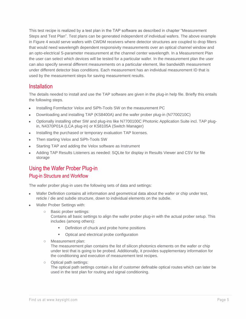
Figure 6. Wafer Data Input Window
Figure 7 shows the list of subdies within a reticle / die on a wafer, including their dimensions and
reference position with respect to the reticle / die origin. This information can be imported from CSV file
and edited in subdie map mask. Subdies in the map can be selected for test.
Figure 7. SubDie Map with Geometrical Information
Figure 8 shows the subdie elements map that includes the list of elements on a selected subdie. The
insert shows the element optical IO port characteristics for the element with ID E001.

P
a
g
e
Find us at www.keysight.com Page 8
Figure 8. List of Device Elements and Example of Element Optical IO Port Characteristics
For better visibility, elements can be labeled and assigned to user defined device classes. The subdie
elements map table contains further useful data:
• Center wavelengths used for alignment.
• Device port numbers. These are used indicate input (stimulus) and output (response) interfaces.
• Coupling direction (e.g. West) for arrays as well as the array pitch and IO type (e.g. surface or edge).
• Incident angle and polarization of operation for grating couplers.
Similar information can be entered for device electrical ports.
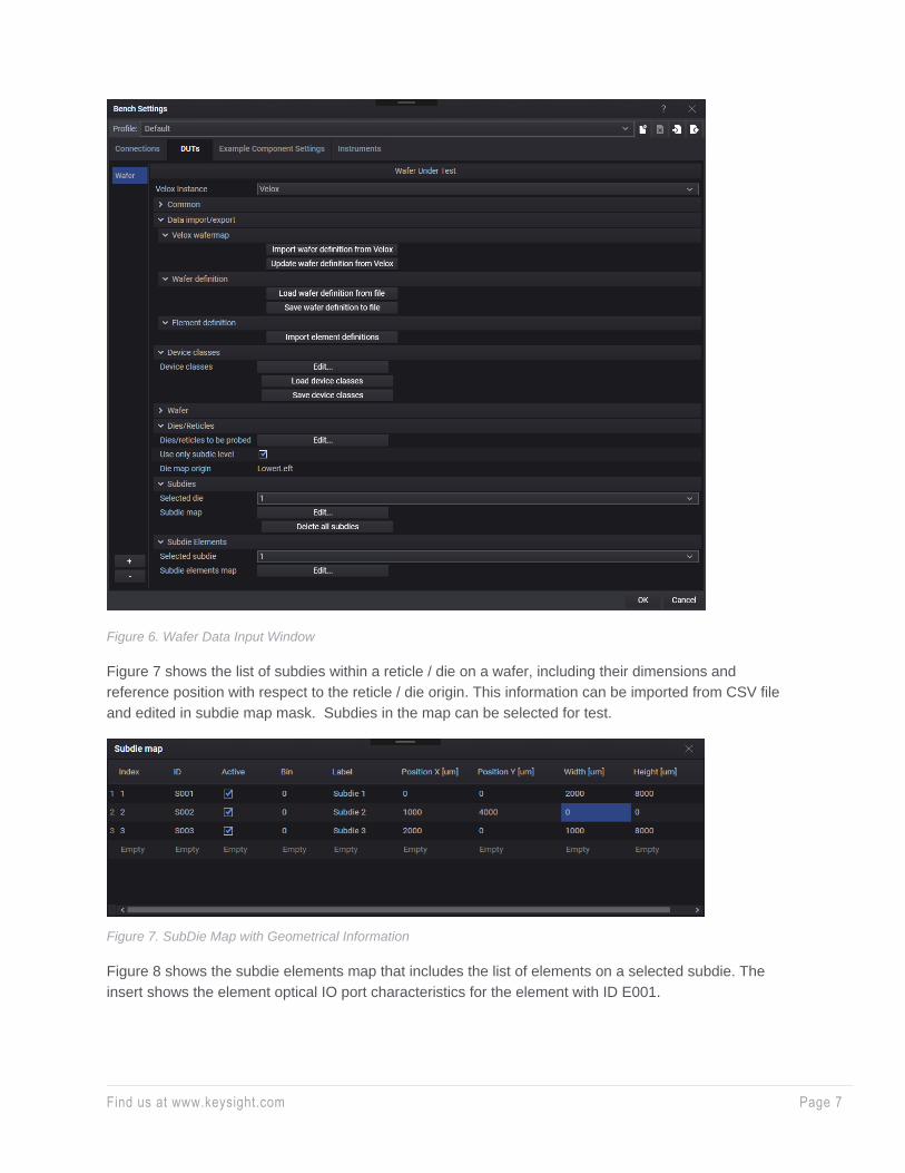
Wafer Prober Settings
Basic Prober Settings
The “Basic Prober Settings” contain all basic settings to align the wafer prober plug-in with the actual
prober setup. This includes (among others):
• Definition of chuck and probe home positions
• Optical and electrical probe configuration
P
a
g
e
Find us at www.keysight.com Page 9
Figure 9. Wafer Prober Settings
Selecting and setting home locations is an essential step in the preparation of an automated
measurement. Home locations for optical or electrical ports can be specified by position information w.r.t.
the subdie origin or by “Selecting by device” from the list of individual subdie elements. This list is
populated from the element definition file that is loaded in the “Wafer Data Input Window” (see Figure 6).
Before starting the test script, the optical and electrical probes need to be positioned at these home
locations in a manual process using the user interface of the wafer prober control SW (e.g. Velox and
SiPh-Tools).
Optical Path Settings
In the “Optical Path Settings” optical routes can be set up between instrument ports and the fiber probes
across multiple optical switches. These routes can be named individually and addressed directly in the
test plan by the “switch optical path” test steps.
Measurement Plan
The “Measurement Plan” allows the user to specify individual measurements on a device. This is useful
for performing measurements on multiport devices with multiple input and output ports. Examples are ring
filter structures with input, add, drop and thru ports, simple 2x2 couplers or balanced detectors connected
to optical 2x2 splitters. Other examples include detector or modulator measurements under various bias
conditions. Each measurement has an individual measurement ID that is used by the measurement
steps. for saving measurement results.
P
a
g
e
Find us at www.keysight.com Page 10
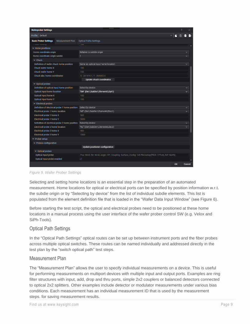
Measurement Steps and Test Plan
The plug-in provides a set of measurement steps that can be added to an automated test plan in TAP.
The desired function can be chosen from the “Steps” panel.
Figure 10. Steps Panel of Wafer Prober Plug-in (Selection)
The steps can then be configured in TAP with the necessary details for the desired measurement.
A typical test plan might look like this:

P
a
g
e
Find us at www.keysight.com Page 11
Figure 11. Sample Test Plan with Prober Steps
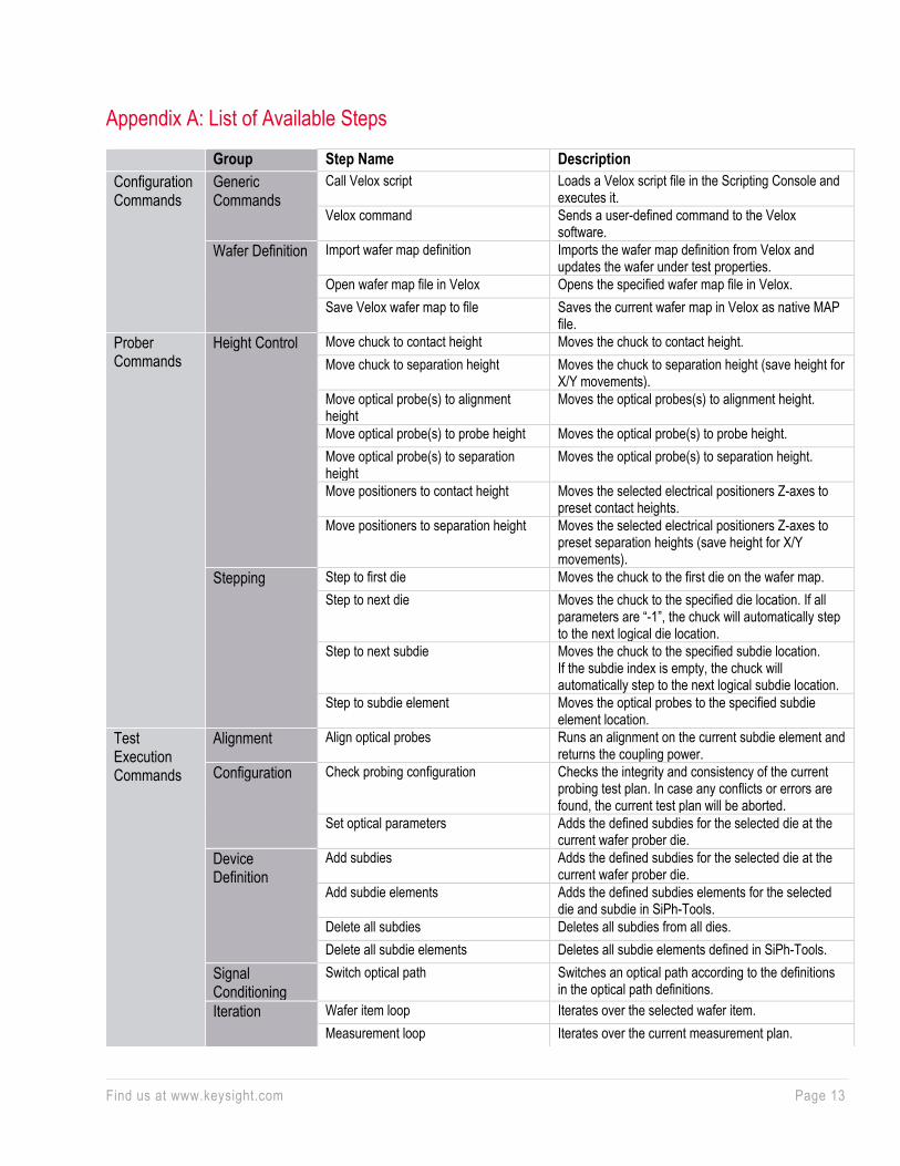
A full list of test steps is provided in the table in “Appendix A: List of Available Steps”.
Once a test plan has been set up, it can be run from the Test Automation Software. A log of the process
is recorded, and flow timing is also displayed (see lower part of Figure 11.)
TAP also provides information of the execution duration of each individual step. This is useful for
optimizing the measurement throughput.
Supported Probe Stations
The N7700210C Wafer Prober TAP Plug-in provides automation for the following Probe Station:
• Formfactor CM300xi with Velox rev.2.5 and Silicon Photonics Tools rev.2.0

P
a
g
e
Find us at www.keysight.com Page 12
Ordering Information
The N7700210C Plug-in is used with the KS8400A TAP software, which requires a separate license. The
system prerequisites for KS8400A apply to use of the plug-in.
Step 1. Choose your software product.
Step 2. Choose your license term: perpetual or time based.
Step 3. Choose your license type: node-locked, transportable, USB portable, or floating.
Step 4. Depending on the license term, choose your support subscription duration.
Products
• N7700210C Wafer Prober TAP Plug-in
• KS8400A Test Automation Platform, Developer’s System
License Type and Terms
Product License type
License term
Perpetual Time-based
License Support subscription License & support
subscription
1
N7700210C
KS8400A
Node-locked (fixed) R-x5y-001-A + R-x6y-001-z R-x4y-001-z
Transportable R-x5y-004-D + R-x6y-004-z R-x4y-004-z
USB Portable1 R-x5y-005-E + R-x6y-005-z R-x4y-005-z
Floating (single site) R-x5y-002-B + R-x6y-002-z R-x4y-002-z
Floating (single region) R-x5y-006-F + R-x6y-006-z R-x4y-006-z
Floating (worldwide) R-x5y-010-J + R-x6y-010-z R-x4y-010-z
z = Subscription duration z = Subscription duration
L 12 months (default) F 6 months
X 24 months L 12 months
Y 36 months X 24 months
Z 60 months Y 36 months
1 USB portable license requires a certified USB dongle (available for additional purchase, Keysight part number E8900-D10)
1
2 3
4
P
a
g
e
Find us at www.keysight.com Page 13
Appendix A: List of Available Steps
Group Step Name Description
Configuration Commands
Generic Commands
Call Velox script Loads a Velox script file in the Scripting Console and executes it.
Velox command Sends a user-defined command to the Velox software.
Wafer Definition
Import wafer map definition Imports the wafer map definition from Velox and updates the wafer under test properties.
Open wafer map file in Velox Opens the specified wafer map file in Velox.
Save Velox wafer map to file Saves the current wafer map in Velox as native MAP file.
Prober Commands
Height Control
Move chuck to contact height Moves the chuck to contact height.
Move chuck to separation height Moves the chuck to separation height (save height for X/Y movements).
Move optical probe(s) to alignment height
Moves the optical probes(s) to alignment height.
Move optical probe(s) to probe height Moves the optical probe(s) to probe height.
Move optical probe(s) to separation height
Moves the optical probe(s) to separation height.
Move positioners to contact height Moves the selected electrical positioners Z-axes to preset contact heights.
Move positioners to separation height Moves the selected electrical positioners Z-axes to preset separation heights (save height for X/Y movements).
Stepping
Step to first die Moves the chuck to the first die on the wafer map.
Step to next die Moves the chuck to the specified die location. If all parameters are “-1”, the chuck will automatically step to the next logical die location.
Step to next subdie Moves the chuck to the specified subdie location. If the subdie index is empty, the chuck will automatically step to the next logical subdie location.
Step to subdie element Moves the optical probes to the specified subdie element location.
Test Execution Commands
Alignment Align optical probes Runs an alignment on the current subdie element and returns the coupling power.
Configuration
Check probing configuration Checks the integrity and consistency of the current probing test plan. In case any conflicts or errors are found, the current test plan will be aborted.
Set optical parameters Adds the defined subdies for the selected die at the current wafer prober die.
Device Definition
Add subdies Adds the defined subdies for the selected die at the current wafer prober die.
Add subdie elements Adds the defined subdies elements for the selected die and subdie in SiPh-Tools.
Delete all subdies Deletes all subdies from all dies.
Delete all subdie elements Deletes all subdie elements defined in SiPh-Tools.
Signal Conditioning
Switch optical path Switches an optical path according to the definitions in the optical path definitions.
Iteration
Wafer item loop Iterates over the selected wafer item.
Measurement loop Iterates over the current measurement plan.
P
a
g
e
Find us at www.keysight.com Page 14
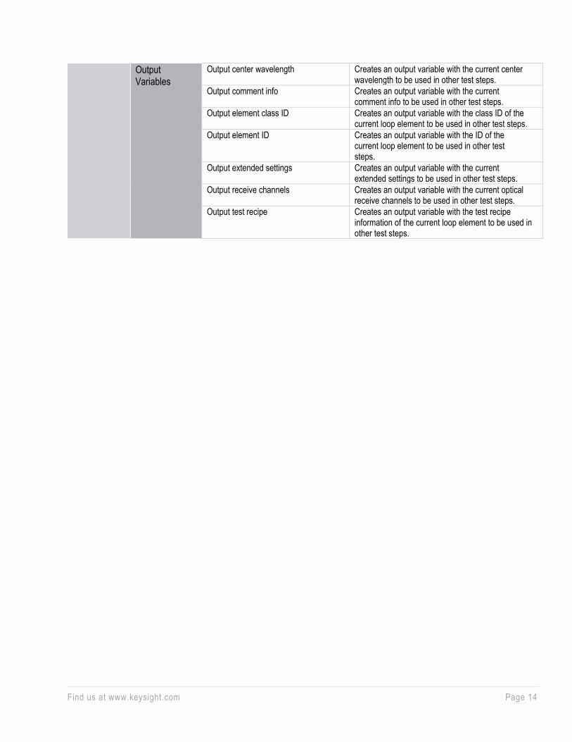
Output Variables
Output center wavelength Creates an output variable with the current center wavelength to be used in other test steps.
Output comment info Creates an output variable with the current comment info to be used in other test steps.
Output element class ID Creates an output variable with the class ID of the current loop element to be used in other test steps.
Output element ID Creates an output variable with the ID of the current loop element to be used in other test steps.
Output extended settings Creates an output variable with the current extended settings to be used in other test steps.
Output receive channels Creates an output variable with the current optical receive channels to be used in other test steps.
Output test recipe Creates an output variable with the test recipe information of the current loop element to be used in other test steps.

P
a
g
e
Find us at www.keysight.com Page 15
Learn more at: www.keysight.com
For more information on Keysight Technologies’ products, applications or services,
please contact your local Keysight office. The complete list is available at:
www.keysight.com/find/contactus
This information is subject to change without notice. © Keysight Technologies, 20 20, Published in USA, April 01, 2020, 3120-1226.EN
Related Literature • PDL Measurement using the Keysight Polarization Controller
• Measuring Polarization Dependent Loss of Passive Optical Components
• Polarization-Resolved Measurements using Mueller Matrix Analysis
• State of the Art characterization of optical components for DWDM applications
• IL and PDL spectra with the N7786B Polarization Synthesizer and the N7700A Photonic
Application Suite
• Programming Keysight Technologies Continuous-Sweep Tunable Lasers
• On-Wafer Testing of Opto-Electronic Components Using the Lightwave Component
Analyzers
• FormFactor’s Autonomous Silicon Photonics Measurement Assistant
• Integrated Photonics Test Brochure
More Information
www.keysight.com/find/N7700210C