integrated UNIFORM LIGHT SOURCE and prober system · 6. Wafer Prober 6.1. Wafer Size Capability 200...
13
TECHNICAL SPECIFICATIONS INTEGRATED UNIFORM LIGHT SOURCE AND PROBER SYSTEM SEMI-CONDUCTOR LABORATORY DEPARTMENT OF SPACE, GOVT. OF INDIA, SECTOR 72, SAS NAGAR, PUNJAB-160071, INDIA
Transcript of integrated UNIFORM LIGHT SOURCE and prober system · 6. Wafer Prober 6.1. Wafer Size Capability 200...

TECHNICAL SPECIFICATIONS
INTEGRATED UNIFORM LIGHT SOURCE AND PROBER SYSTEM
SEMI-CONDUCTOR LABORATORY DEPARTMENT OF SPACE, GOVT. OF INDIA,
SECTOR 72, SAS NAGAR, PUNJAB-160071, INDIA

i
Contents
1. Introduction .................................................................................................................. 1
2. Scope of Supply ........................................................................................................... 1
3. Scope of Installation, Testing and Commissioning ........................................................ 1
4. Technical Specifications ............................................................................................... 1
4.1. Uniform Light Source ........................................................................................................... 2
4.2. Semi-Automatic Wafer Prober............................................................................................ 5
4.3. Semi-Automatic Prober and Light Source Integration .................................................... 7
4.4. Software and Development Tools ...................................................................................... 8
4.5. Certifications ......................................................................................................................... 9
5. Acceptance Criteria .................................................................................................... 10
6. Warranty .................................................................................................................... 10
7. Duration ..................................................................................................................... 11
8. Safety ......................................................................................................................... 11
9. Eligibility Criteria ......................................................................................................... 11
10. Post Warranty Support ............................................................................................... 11
11. Training ...................................................................................................................... 11
12. Calibration .................................................................................................................. 11
13. Other Conditions ........................................................................................................ 11

ANNEXURE I
1
1. Introduction Semi-Conductor Laboratory (SCL), is engaged in the design and development of
semiconductor devices for various applications. SCL intends to procure an Integrated Uniform
Light Source and Prober System to characterize the Imager dies for optical response,
cosmetic defects and non-uniformity measurements at wafer level.
2. Scope of Supply 2.1. Supply of Uniform Light Source System and Semi-Automatic Wafer Prober as per the
technical specifications defined in this document including integration of the Uniform Light
Source System and Semi-Automatic Wafer Prober
2.2. Supply of software and functional LabVIEW palettes for Prober, Light Source and their
Integrated operations.
2.3. Any item(s) not specifically mentioned in the specifications but required for safe and
efficient operations of the system should deemed to be included in the scope of supply of
the vendor(s) unless explicitly indicated in the bid by the vendor(s).
2.4. The equipment offered should be of latest design and represent state of art technology in
machine tool and control system design/manufacture. The equipment shall be rated for
continuous heavy duty to work round the clock without stoppage. All electrical and
electronic components are to be tropicalized.
3. Scope of Installation, Testing and Commissioning 3.1. Installation of Semi-Automatic Wafer Prober and Uniform Light Source System and
integration of the same to have an operational Integrated Uniform Light Source and
Prober System meeting the defined technical specifications.
3.2. Testing and commissioning of Semi-Automatic Wafer Prober, Uniform Light Source
System and the Integrated System.
3.3. Performance demonstration of Semi-Automatic Wafer Prober, Uniform Light Source
System and the Integrated System meeting the defined technical specifications.
4. Technical Specifications Typical Block diagram of wafer level Imager characterization set-up is shown in figure 1 below.
Figure 1: Typical Block diagram of Wafer level Imager characterization Set-up

ANNEXURE I
2
Detailed specifications of the system is given below.
4.1. Uniform Light Source The uniform light source shall comprise of lamps & optical system, integrating sphere, filters,
attenuators, light measurement system, calibrated Si detector, calibrated spectral irradiance
meter, calibrated pico-ammeter, controlling unit, power supply, etc. The lamps shall be of
either QTH/Xe/Plasma providing desired irradiance in specified bands. Heat absorbing Filters,
Narrow Band-Pass Filter and Broad Band-Pass Filter shall be mounted on different filter
wheels for automatic selection of either one filter or combination of filters. The attenuator and
filters shall be assembled to provide accessibility to add/replace new filter(s). Light
mixers/integrating sphere shall have coating reflectance better than 96%. The collimated lens
system at the exit port of integrating sphere will collimate uniform light (≥98%) on device wafers
under test allowing sufficient working distance.
Typical Block diagram of Uniform Light Source System is shown in figure 2 below.
Figure 2: Typical Block diagram of Uniform Light Source System
The light source should be capable of projecting high irradiance but less than <1mW/cm2,
collimated light on DUT placed over wafer chuck. Light source system shall allow selection of
either narrow band spectral light or broad band spectral light based on the user requirement.
The heat absorbing filter shall be placed on separate filter wheel for either selection or bypass.
Vendor to provide PC controlled, software based selection of different narrow band or broad
band light projection on DUT.
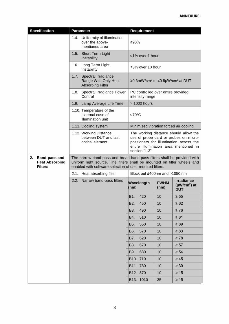
Table 1: Specifications of Uniform Light Source System
Specification Parameter Requirement
1. Uniform Light Source
1.1. Spectral Range ≤400 to ≥1050nm
1.2. Colour Contrast Temperature of Light Source
3000 to 5200 K
1.3. Area of Uniform Illumination
Circular: ≥5 cm to ≤10cm diameter OR
Rectangular: 4.2 cm x 2.5 cm
ANNEXURE I
3
Specification Parameter Requirement
1.4. Uniformity of Illumination over the above-mentioned area
≥98%
1.5. Short Term Light Instability
≤1% over 1 hour
1.6. Long Term Light Instability
≤3% over 10 hour
1.7. Spectral Irradiance Range With Only Heat Absorbing Filter
≥0.3mW/cm2 to ≤0.8μW/cm2 at DUT
1.8. Spectral Irradiance Power Control
PC controlled over entire provided intensity range
1.9. Lamp Average Life Time ≥ 1000 hours
1.10. Temperature of the external case of illumination unit
≤70°C
1.11. Cooling system Minimized vibration forced air cooling
1.12. Working Distance between DUT and last optical element
The working distance should allow the use of probe card or probes on micro-positioners for illumination across the entire illumination area mentioned in section “1.3”
2. Band-pass and Heat Absorbing Filters
The narrow band-pass and broad band-pass filters shall be provided with uniform light source. The filters shall be mounted on filter wheels and enabled with software selection of user required filters.
2.1. Heat absorbing filter Block out ≤400nm and ≥1050 nm
2.2. Narrow band-pass filters
Wavelength (nm)
FWHM (nm)
Irradiance (µW/cm2) at DUT
B1. 420 10 ≥ 55
B2. 450 10 ≥ 62
B3. 490 10 ≥ 76
B4. 510 10 ≥ 81
B5. 550 10 ≥ 89
B6. 570 10 ≥ 83
B7. 620 10 ≥ 78
B8. 670 10 ≥ 57
B9. 680 10 ≥ 54
B10. 710 10 ≥ 45
B11. 780 10 ≥ 30
B12. 870 10 ≥ 15
B13. 1010 25 ≥ 15

ANNEXURE I
4
Specification Parameter Requirement
2.3. Wide band-pass filters Wavelength (nm)
FWHM (nm)
Irradiance (µW/cm2) at DUT
B14. 425 50±5 ≥ 300
B15. 550 50±5 ≥ 630
B16. 650 50±5 ≥ 444
B17. 825 50±5 ≥ 255
The minimum irradiance level achievable shall be ≤0.8 µW/cm2 at DUT in presence of heat absorbing filter and wide band pass filter
2.4. Out of Band Light Transmission
≤ 0.01%
2.5. Peak Transmission in Band-Pass Region
≥80%
2.6. Centre Wavelength Tolerance
B1 to B12: ±2 nm or better
B13: ±5 nm or better
B14 to B17: ±5 nm or better
2.7. FWHM Tolerance B1 to B12: ±2 nm or better
B13: ±3 nm or better
2.8. Operating Temperature Filters to demonstrate above specification when operated up to 300°C for normal operation (non-condensing and RH<50%)
2.9. Filter life time >2000hrs at 300°C under continuous operation (non-condensing and RH<50%).
2.10. Variable Attenuator PC Controlled 8 decade resolution with 2 million steps. Vendor to provide attenuator position versus illumination intensity curves for attenuator(s).
2.11. Filter Arrangement Filter wheel or other filter assembly mechanism for automatic selection of one or three filters for simultaneous use. One heat absorbing filter and narrow band filter or wide band filter. It should support software-controlled change of filters which need to be swapped between measurements. Each wheel-mounted filter shall be user-replaceable with new set of filters and at least one wheel must have one empty slot. Vendor to provide filter holder for filters of standard dimension available in market.
3. Light Measurement System
3.1. Detector Type Silicon Detector
3.2. Detector Response Range
≤400 to ≥1050nm
3.3. Detector Area 1mm x 1mm or more

ANNEXURE I
5
Specification Parameter Requirement
3.4. Operating Temperature Range
Within 30°C to -30°C
3.5. Detector’s Noise Equivalent Power
0.02 nW/√Hz or less
3.6. Readout Unit Accuracy ±2% or better for >200nA
3.7. Minimum Detectable Power
80 nW or less
3.8. Calibration certificate NIST/PBT traceable calibration certificate
4. Spectral Irradiance Meter
4.1. Wavelength Range ≤400 nm to ≥1100 nm
4.2. Wavelength Resolution ≤1 nm
4.3. Luminous Intensity Accuracy
±1%
4.4. Computer Interface USB/GPIB/Ethernet
4.5. Calibration certificate NIST/PBT traceable calibration certificate
5. Spares 5.1. Lamps
05 numbers with identical specs (along with its test results operated for 10 hours at vendor premises)
5.2. Filter Sets Supply (1) complete set of spare filters (heat absorbing, narrow band-pass and wide band-pass filters) with system.
4.2. Semi-Automatic Wafer Prober
The prober shall be standard 200 mm wafer prober platform compatible for integrating with
the Uniform Light Source System. The semi-automatic wafer prober shall have automatic
wafer alignment with auto correction capability in XYZ and theta stages. The prober shall have
rollout stage which provides complete wafer access for safe and easy loading. The rollout
stage shall contain a low leakage wide temperature range thermal chuck. The platen shall
have connector panel provided with triaxial and co-axial connectors. The prober shall be
operated using standard sized probe cards consisting of passive electronic components. The
specifications of wafer prober are tabulated below:
Table 2: Specifications of Semi-automatic wafer prober
Specification Parameter Requirement
6. Wafer Prober 6.1. Wafer Size Capability 200 mm, 150 mm, 100 mm wafers and single die of size greater than 1 cm x 1 cm
6.2. Wafer Handling Single wafer, manual feed type
6.3. Semi-automation One step manual align teach and automatic die stepping
7. Chuck XY Stage 7.1. Travel 203 mm x 203 mm
7.2. Resolution ±1 μm or better
7.3. Accuracy ≤2.5 μm

ANNEXURE I
6
Specification Parameter Requirement
7.4. Speed ≥30 mm/s
8. Chuck Z Stage 8.1. Travel ≥5 mm
8.2. Resolution 1 μm or better
8.3. Accuracy ≤2 μm
9. Theta Stage 9.1. Travel ±5° range of motion
9.2. Resolution 0.01° motorized stage movement
9.3. Accuracy 0.1°
10. Chuck 10.1. Chuck Flatness ≤10 μm
10.2. Thermal Operation in the Range
-55ºC to 180ºC (±1ºC)
10.3. Chuck Leakage ≤ 2fA
10.4. Residual Capacitance ≤ 2.5pF
11. Platen 11.1. Lift ≥5 mm
11.2. Connectors Triaxial to co-axial and vice-versa
12. Micro-positioners
12.1. Feature Resolution ≤2 μm
12.2. Travel in X, Y, Z axis 8 mm
12.3. Probe Arms and Cables Six number fully shielded triaxial up to probe tip
12.4. Probe Tips 10 μm, 19 μm (six number each)
12.5. Base Vacuum/Magnetic
12.6. Application IV/CV probing for interfacing with Agilent B1500 and probe card holder
12.7. Quantity Six numbers
13. Micro chamber 13.1. EMI shielding ≥ 20 dB 0.5-3 GHz
13.2. System AC noise ≤ 20 mVp-p
14. Microscope & Video Camera
14.1. Type High magnification colour CCD/CMOS digital microscope system
14.2. Field of View 13mm x 9mm or more under lowest magnification
14.3. Maximum Magnification 200x
14.4. Translation Stage for Digital Microscope
±5cm horizontal movement in each X and Y direction to focus the either edges of 10cm DUT. The vibration free movement of translation stage to ensure safe probing.
14.5. Video Display Dual flat LED colour monitor for probe viewing and computer display
15.1. Table Top Steel

ANNEXURE I
7
Specification Parameter Requirement
15. Vibration Isolation
15.2. Vertical & Horizontal Natural Frequency
Typical performance better than 0dB at 6Hz, with -6 dB per octave roll-off to 48Hz and >-18 dB attenuation above 48Hz (with a semi-automatic 8” probe station or equivalent load)
16. Probe Card Compatibility
16.1. Dimension 4.5 inch up to 8 inch long
16.2. Clearance Space Between Probe Card Holder and Platen
≥7.5 mm
17. Computer 17.1. Operating System Windows 7 or higher
17.2. Processor Intel i5 or better
17.3. RAM and HDD ≥ 4 GB and ≥ 240 GB
In case the vendor wishes to provide alternate approach(s) to relate the defined
technical specifications of the integrated Uniform Light Source and Prober System, he
may submit the same including the corresponding Block Diagram along with their
technical bid. The same will be evaluated by SCL as part of the technical evaluation.
4.3. Semi-Automatic Prober and Light Source Integration
The Wafer Prober shall be seamlessly integrated with Uniform Light Source for computer
controlled operation of complete system. The light source shall be permanently fixed with
prober facing the wafer chuck vertically down when placed on wafer prober. The working
distance between light source and wafer chuck should allow the use of probe card or probes
on micro-positioners for illumination across the entire illumination area and to measure
uniformity of light over illumination area using Si detector mounted within wafer chuck and by
controlling chuck temperature. The light source and microscope may be placed on single
platform over wafer prober to select either of them as per requirement. At a fixed position on
the platform, light source shall have automatic XY movement control. However Z movement
of light source may be manual for occasional use. The specifications defines integration of
prober and light source are as below:
Table 3: Specifications for integration of Prober and Uniform Light Source
Specification Parameter Requirement
18. Integration of Uniform Light Source and Wafer Prober
18.1. Positioning of Light Source
Light source shall face the wafer vertically down when placed on wafer prober.
18.2. Light Source and Microscope
Suitable arrangement shall be made to select either light source or video camera one at a time with easy inter-changeability between the two.
18.3. Translation Stage for Light Source
±5cm horizontal automated movement in each X and Y direction from nominal centre of spot on DUT. The X and Y movements shall be independent of each other. The manual Z movement of ±2.5 cm. The vibration free movement of translation stage to ensure safe probing.
ANNEXURE I
8
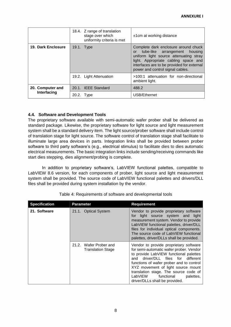
18.4. Z range of translation stage over which uniformity criteria is met
±1cm at working distance
19. Dark Enclosure 19.1. Type Complete dark enclosure around chuck or tube-like arrangement housing uniform light source attenuating stray light. Appropriate cabling space and interfaces are to be provided for external power and control signal cables.
19.2. Light Attenuation >100:1 attenuation for non-directional ambient light.
20. Computer and Interfacing
20.1. IEEE Standard 488.2
20.2. Type USB/Ethernet
4.4. Software and Development Tools
The proprietary software available with semi-automatic wafer prober shall be delivered as
standard package. Likewise, the proprietary software for light source and light measurement
system shall be a standard delivery item. The light source/prober software shall include control
of translation stage for light source. The software control of translation stage shall facilitate to
illuminate large area devices in parts. Integration links shall be provided between prober
software to third party software’s (e.g., electrical stimulus) to facilitate dies to dies automatic
electrical measurements. The basic integration links include sending/receiving commands like
start dies stepping, dies alignment/probing is complete.
In addition to proprietary software’s, LabVIEW functional palettes, compatible to
LabVIEW 8.6 version, for each components of prober, light source and light measurement
system shall be provided. The source code of LabVIEW functional palettes and drivers/DLL
files shall be provided during system installation by the vendor.
Table 4: Requirements of software and developmental tools
Specification Parameter Requirement
21. Software 21.1. Optical System Vendor to provide proprietary software for light source system and light measurement system. Vendor to provide LabVIEW functional palettes, driver/DLL files for individual optical components. The source code of LabVIEW functional palettes, driver/DLLs shall be provided.
21.2. Wafer Prober and Translation Stage
Vendor to provide proprietary software for semi-automatic wafer prober. Vendor to provide LabVIEW functional palettes and driver/DLL files for different functions of wafer prober and to control XYZ movement of light source mount translation stage. The source code of LabVIEW functional palettes, driver/DLLs shall be provided.

ANNEXURE I
9
4.5. Certifications
The vendor shall provide following test reports/data sheets/documents at the stages
mentioned in the below table.
Specification Requirement Phase
22. Calibration Certificate, Test Reports, Data Sheets and Documents
22.1. Measurement procedures and list of equipment to be brought to SCL and to demonstrate parameters during installation and commissioning
With Technical bid
22.2. Out of band Transmission characteristics of all filters for different temperature up to 300˚C
Factory test results during Integration
22.3. Central peak wavelength transmission characteristics of all filters for different temperature
Factory test results during Integration
22.4. NIST/PTB traceable calibration certificate for Si detector, lamps and current measurement unit
Factory test results during Integration
22.5. Spectral range (400 to 1050 nm) and area of illumination
Factory test results during Integration
22.6. Uniformity of illumination for every 0.5 mm2 block in the defined illumination area for different wavelengths
Factory test results during Integration
22.7. Demonstration of spectral irradiance range for all band-pass filters
Factory test results during Integration
22.8. Stability of light over 1 hour and 10 hour period
Factory test results during Integration
22.9. FWHM deviation against the expected value for all filters
Factory test results during Integration
22.10. The X and Y automatic movement of translation stage for light source covering 15cmx15cm illumination area
Factory test results during Integration
22.11. Thermal chuck temperature operation range and temperature control calibration
Factory test results during Integration
22.12. Parallelism of wafer chuck to uniform light source
Installation and Commissioning
22.13. Variable attenuator steps versus irradiance values for different bands
Installation and Commissioning
22.14. Data sheets and manuals of third party components (like Si detector, filters, variable attenuators, spectral irradiance meter, pico-ammeter, filter wheels, motorized stage of light source mount, etc) used to build complete unit
Installation and Commissioning

ANNEXURE I
10
5. Acceptance Criteria SCL engineers may inspect the Integrated Light Source and Prober for witnessing the factory
tests. The waiver of factory inspection by SCL shall however not absolve the vendor of its
responsibilities for demonstration of functionality and other acceptance criteria on installation
at SCL.
Table 5: Conditions for Tool acceptance criteria
Specification Requirement
23. Acceptance Criteria
23.1. Calibration certificates, test reports, software, drivers, source code, operator’s manual, service & maintenance manual and documents mentioned in 22 shall be provided at designated phases of procurement and during installation.
23.2. Factory test results meeting the technical specifications as specified in 22 to be submitted before equipment shipment.
23.3. On installation of this equipment, vendor shall demonstrate the parameters mentioned in 22.5, 22.6, 22.7, 22.8, 22.9, 22.10, 22.11, 22.12 and 22.13 of the technical specifications using the measurement tests/equipment brought to SCL. Vendor shall also submit complete test plan for demonstration of above parameters along with technical offer.
23.4. Vendor shall demonstrate the successful functionality of the integrated system for continuous 8 hours operation. Repeatability tests after every 24 hours for three times shall meet the technical specifications.
Deliverables
The deliverables shall include but not limited to
24. Deliverables Items Quantity
24.1. Integrated Light Source and Prober System
01
24.2. Software and drivers 01 set
24.3. Spare lamps 05
24.4. Spare filters
(narrow band-pass, broad band-pass and heat absorbing)
01 set
24.5. Manuals, Certificates and Test Reports
(Soft copy and hard copy as applicable)
01 set
24.6. Mechanical tool set 01 set
6. Warranty and AMC 6.1. Vendor shall provide minimum twenty four months on-site warranty on Integrated Light
Source and Prober System and its accessories from the date of successful
commissioning and acceptance of the system.
6.2. Vendor shall provide two Preventive Maintenance visits during the warranty period of
Integrated set-up.
ANNEXURE I
11
6.3. Vendor shall also give its offer for comprehensive AMC (including one on-call service
visit per year) for five years after the expiry of warranty period.
7. Duration 7.1. Vendor shall specify the total time required for execution of the Purchase Order, meeting
the timeline for major milestones like integration & factory acceptance, installation &
commissioning.
8. Safety 8.1. The Integrated set-up shall be comply with safety standards like CE standards, etc.
8.2. Appropriate safety/statutory warning messages should be pasted on integrated set-up
and its sub-systems.
9. Eligibility Criteria 9.1. Only those prospective vendors are eligible to bid who have supplied, installed and
successfully commissioned Semi-Automatic Wafer Prober/Uniform Light source
System/Integrated Uniform Light Source System & Semi-Automatic Probe System, in
the last seven years. Documents evidencing the said installations shall be submitted by
the vendor along with the technical bids to ascertain their eligibility to participate in the
tender.
9.2. The vendor (Prime Bidder) may form a consortium comprising of one or two or more
vendors for bidding and execution of the Purchase Order. However, the responsibility for
the entire system shall rest with the Prime Bidder.
10. Post Warranty Support 10.1. Vendor shall guarantee supply of spares and services support for at least ten years post
installation of the equipment.
11. Training 11.1. During commissioning of integrated set-up, vendor(s) should provide on-site hands-on-
training to the concerned SCL personnel on operations, software, trouble-shooting and
preventive maintenance of the set-up.
11.2. The training should be extensively conducted for four days covering above mentioned
aspects.
12. Calibration 12.1. The validity of calibration certificates should be at least twelve months from the date of
successful installation of the equipment at SCL.
12.2. Vendor shall quote calibration charges at user site after warranty
13. Other Conditions 13.1. All essential spares and consumables for trouble free operation of the equipment for a
period of at least five years shall be item wise quoted separately.
13.2. Vendor(s) shall provide one set of Technical documents (printed in English) on Test
Manual(s) and operational manual to SCL.
13.3. Vendor to specify the facilities required according to the format given in Annexure III.