VLV7HFKQLTXH Selma M.H. Al-Jawad · Vol 23, No. 2;Feb 2016 189...
16
Vol 23, No. 2;Feb 2016 185 [email protected] Influence of Cadmium Doping on Structural, Optical, electrical and Photocatalytic properties of TiO2 Thin Films Prepared by Spray Pyrolysis Technique Jawad - Al Selma M.H. School of Applied Sciences, University of Technology, Baghdad, IRAQ E-mail: Salma [email protected] Abstract Undoped and doped cadmuim titanium oxide thin films at different percentage (1, 3, 4, and 5) % were fabricated by spray pyrolysis by using a solution of titanium tetrachloride and ethyl alcohol. The films have been deposited on heated quartz substrates at 623 K. After annealing for 120 min at 823 K, the initially amorphous films became polycrystalline with a predominant anatase structure and average crystallite sizes depending on dopant Cd concentration. Atomic force microscope (AFM) results show that the addition of the Cd to TiO2 thin films become smooth. Optical study shows the optical band gap, and transmission has been increasing with increasing doping concentration in TiO2 thin films. The electrical resistivity is decreases with increasing doping concentration Cd in TiO2 thin films could be attributed to the increasing charge concentration. Photocatalytic activity of the TiO2 films were studied by monitoring the degradation of aqueous methylene blue under UV light irradiation and was observed that increasing doping concentration had good photocatalytic activity which was explained as due to the structural and morphological properties of the films. Keywords: TiO2, Spray Pyrolysis, cadmium dopent, Structural Properties, Optical Properties, and photocatalytic properties. 1. Introduction Over the last few years a great attention has been focused on the titanium dioxide (TiO2) thin films because its excellent materials in many applications, such as in the field of sensors, antireflection coatings, gas sensors[1], solar cells[2]and photocatalysis[3,4]. By doping, especially www.spm.com.cn
Transcript of VLV7HFKQLTXH Selma M.H. Al-Jawad · Vol 23, No. 2;Feb 2016 189...

Vol 23, No. 2;Feb 2016
Influence of Cadmium Doping on Structural, Optical, electrical and Photocatalytic properties of TiO2 Thin Films Prepared by Spray Pyrolysis Technique
Jawad-Al Selma M.H. School of Applied Sciences, University of Technology, Baghdad, IRAQ
E-mail: Salma [email protected]
Abstract
Undoped and doped cadmuim titanium oxide thin films at different percentage (1, 3, 4, and 5) %
were fabricated by spray pyrolysis by using a solution of titanium tetrachloride and ethyl alcohol.
The films have been deposited on heated quartz substrates at 623 K. After annealing for 120 min at
823 K, the initially amorphous films became polycrystalline with a predominant anatase structure
and average crystallite sizes depending on dopant Cd concentration. Atomic force microscope
(AFM) results show that the addition of the Cd to TiO2 thin films become smooth. Optical study
shows the optical band gap, and transmission has been increasing with increasing doping
concentration in TiO2 thin films. The electrical resistivity is decreases with increasing doping
concentration Cd in TiO2 thin films could be attributed to the increasing charge concentration.
Photocatalytic activity of the TiO2 films were studied by monitoring the degradation of aqueous
methylene blue under UV light irradiation and was observed that increasing doping concentration
had good photocatalytic activity which was explained as due to the structural and morphological
properties of the films.
Keywords: TiO2, Spray Pyrolysis, cadmium dopent, Structural Properties, Optical Properties, and
photocatalytic properties.
1. Introduction
Over the last few years a great attention has been focused on the titanium dioxide (TiO2) thin
films because its excellent materials in many applications, such as in the field of sensors,
antireflection coatings, gas sensors[1], solar cells[2]and photocatalysis[3,4]. By doping, especially
www.spm.co
m.cn

Vol 23, No. 2;Feb 2016
with transition metal atoms, these properties can be improved as desired, while keeping the films
chemical and mechanical stability [1].
There are many methods that can be used to prepare TiO2 thin films with desired properties
including sol–gel[4-7], sputtering[8], anodic oxidation[9-14], pulsed laser deposition (PLD)[15],
and spray pyrolysis[1-3,16-18]. Of all the afore-mentioned thin film fabrication methods, spray
pyrolysis is widely used because of its simplicity, cheap chemical deposition procedure, allowing
the growth of rough-surface films at atmospheric pressure, on large area. By this method, dopants
can be easily introduced into the matrix of the film by using appropriate precursors [1, 16].
In this paper we have investigated the effect of cadmium doping on structure, optical , electrical
and photocatalytic properties of TiO2 thin films prepared by spray pyrolysis.
2. Experimental work
Undoped and cadmium-doped titanium oxide thin films were deposited on heated quartz substrate
(623 K), by spraying an appropriate solution from a sprayer, placed at 30 cm in front of the heated
substrate holder.
The starting solution was prepared by using (2 ml) titanium tetrachloride (TiCl4, purity 99.9%,
1.726g/cm3 density) which is made in "England" dissolved in (20 ml) ethyl alcohol (96%).
Filtered air was used as a carrier gas, the deposition time was set to 5 sec, the (undoped and doped)
samples were annealed at 823 K in air for 120 min. Salt[CdCl2.6H2O] are used to dope TiO2 films
for different percentages (1,3,4 and 5%) of dopant.
The structural properties of the prepared films were studied by X-ray diffraction measurements
(Philips PW 1050 X-ray diffractometer, with CuKα radiation (λ= 1.54059 Å)). The morphology of
the films was studied by Scanning Electron Microscopy (SEM) type VEGA TE SCAN equipment
operated at 30 keV. AFM studies were performed using a scanning probe microscopy (CSPM-
5000). After annealing in the air the electrodes were deposited onto film surface by thermal
evaporation of aluminum in vacuum system. The Edward E 306A coating system was used for this
purpose, under pressure of about 10-5 torr. The best condition for good ohmic contact was satisfied
by a layer of 200 nm. To study the electrical characterization of the TiO2 films, electrical
resistivity measurements were performed using two point probe method.
The current measurements carried out by applying voltage supplied to the sample from a
www.spm.co
m.cn
zhk
铅笔

Vol 23, No. 2;Feb 2016
stabilized d.c. fine power supply, type L 30 – 2 Farnell of range (0.1 – 5)V. The current passing
through the sample was measured using a Keithley (602) electrometer.
Ellipsometer equipped with a He-Ne laser source (λ= 632.8 nm) were conducted to calculate film
thickness. UV- VIS Spectrophotometer was used to measure the transmittance of TiO2 films
within the wavelength range of (300- 1100 nm). Using the optical transmittance spectra, the
absorption coefficient and the band gap of TiO2 were evaluated.
The photocatalytic activity of TiO2 films was evaluated from the degradation of methylene blue
(MB) during its catalytic decomposition. The MB (C16H18ClN3S) is an organic water soluble
cationic dye found in waste waters and is potentially toxic. An aqueous solution of MB (100 mg/l)
was taken in the reactor and was constantly stirred. The pH of the solution was adjusted to 3 with
dilute hydraulic acid was added. The quartize slide coated with TiO2 film of area 4.5 cm2 was
immersed in to the MB solution. Initially the MB solution with TiO2 film was kept in dark for 30
min to establish adsorption–desorption equilibrium. After this stabilization period the TiO2 film
was irradiated with ultraviolet (UV) light source with central wavelength emission at 365 nm. The
absorbance of the MB solution was monitored at intervals of 30 min using a UV–Vis
spectrophotometer. The rate of photodegradation of MB solution in the case of each film was
analyzed by monitoring the intensity variation of the main absorption band of MB at 605 nm.
3. Result and Discussion
3.1. X-Ray Diffraction study
The crystal structure of TiO2 films was investigated through X-ray diffraction (XRD). The X-ray
diffraction spectrum of pure and doping TiO2 films with cadmium for different doping
concentration (1,2,3,4 and 5) % deposited on quartz substrate at annealing temperature(823 K)
for (120min ) are shown in Fig. (1). It is found that all the films are polycrystalline with a
tetragonal crystal structure. All films show diffraction peaks belong to anatase A(101). The
diffraction peaks are in good agreement with those given in JCPD data card (JCPDS no .21-1272)
for anatase phase. It is observed that the pure TiO2 films exhibit a polycrystalline having (101),
(004) and (200) planes of high peak intensities. The doped titanium oxide films become less
crystalline than undoped sample. The crystal size was calculated from the full width at half
www.spm.co
m.cn

Vol 23, No. 2;Feb 2016
maximum (FWHM) (β) of the preferential orientation diffraction peak by using the Scherrer
equation [16]
D = kλ / (βCosθ) (1)
where D is the crystallite size, k is a fixed number of 0.9, λ is the X-ray wavelength, θ is the
Bragg’s angle in degrees, and β is the full-width-at- half maximum (FWHM) of the chosen peak.
Compared to the reference data from TiO2 (JCPD) card, the peaks in the X- Ray diffraction shift
into the region of higher 2θ, indicating stress in the grains. Increasing in full-width at half-
maximum (FWHM) of (101) peak means decrease crystal size of film with the increase doping
concentration in TiO2 films as shown in Fig. (2). This result agrees well with literature [1]. XRD
analysis also did not detect the dopant phase, this is due to the low concentration of dopants, in
previous work by other group[1]. Results of TiO2: Cd at different doping concentration on the
films structure is given in Table (1).
The anatase phase is having a tetragonal unit cell and the lattice parameters (a, c) can be calculated
from the peak positions (0 0 4) and (2 0 0) using the relations a = b = 2 × d004 and c = 4 × d200 [4,
19]. Increases in doping concentration in TiO2 films result in the increasing lattice constant (a),
this can be attributed to increase in interplanar distance (d) according to above equations. The
lattice parameters calculated for the undoped films were a = 3.7914 ˚A and c = 9.5898 ˚A. This is
close to the reported bulk values of anatase phase (a = 3.7842 ˚A, c = 9.5146 ˚A). The dependence
of the lattice parameters on doping concentration is shown in Fig. 2 B. It can be observed that the
lattice constant a decreases with the increasing doping concentration where as the lattice constant c
increases with it. In the case of films undoped films the ratio of lattice constants c/a was 2.52 ˚A
which is higher than the c/a value (2.5142 ˚A) of the stress free TiO2. Therefore increases in
doping concentration in TiO2 films lead to increase of the lattice constant ratio c/a these means the
lattice under the stress [4]
www.spm.co
m.cn

Vol 23, No. 2;Feb 2016
0
100
200
300
400
500
600
700
20 25 30 35 40 45 50 55
Inte
nsi
ty
2Theta(deg)
A(101)
A(004) A(200)
pure
m at different films pure and doping with cadmiu 2Fig. ( 1 ) :XRD patterns of TiO
pure (B) 1% (C)3% (D)4% (E)5%. 2concentrations(A) TiO
0
50
100
150
200
250
10 20 30 40 50 60
2θ(deg)
Inte
nsi
ty
101
0
50
100
150
200
250
300
10 20 30 40 50 60
2θ(deg)
Inte
nsi
ty
3%Cd
0
50
100
150
200
250
10 20 30 40 50 60
2θ(deg)
Inte
nsi
ty
0
50
100
150
200
250
10 20 30 40 50 60
2θ(deg)
Inte
nsi
ty
5%
004 200
1%
004 200
3|%
004
101 101
200
4%
101
004 200
A B
C D
E
www.spm.co
m.cn

Vol 23, No. 2;Feb 2016
concentrations. pingat different do 2Table(1): Experimental results for TiO
doping 2TiO
with Cd
2(θ)
deg hkl
β
(deg)
Crystal size
(nm)
a=b
)̊Ao(
c
A)o( c/a
2Undoped TiO 25.27 A(101) 0.272 29.87 3.7914 9.58989 2.5200
1% 25.6116 A(101) 1.11970 7.2822 3.786 9.61188 2.5293
3% 25.1 A(101) 2.400 3.393 3.7803 9.6922 2.5387
4% 25.4268 A(101) 3.54960 2.295 3.7803 9.755 2.5638
5% 24.0258 A(101) 6.75410 1.2030 3.77964 9.804 2.5938
Fig. ( 2) :(A) The main grain size and Full Width at Half Maximum (FWHM) for TiO2 films
A (101) at different doping concentration of cadmium. (B) The plot of the variation of
lattice constants ‘‘a” and ‘‘c” as a function of annealing temperature. The lattice constant
‘‘a” was calculated from the X-ray peak (0 0 4) and lattice constant ‘‘c” was calculated from
peak (2 0 0).
3.77
3.775
3.78
3.785
3.79
3.795
0 2 4 6doping concentration %
Latt
ice p
ara
mete
r a (
OA
)
9.55
9.6
9.65
9.7
9.75
9.8
9.85
Lattic
e p
ara
mete
r c (
oA)
Lattice parameter a
Lattice parameter c
012345678
0 1 2 3 4 5 6
Dopping concentration %
Cry
sta
l S
ize (
nm
)
012345678
FW
HM
(d
eg
)
FWHM
Grain size
.
A B www.spm.co
m.cn

Vol 23, No. 2;Feb 2016
3.2. AFM study.
Fig. 3 shows the surface morphology micrographs of undoped and Cd-doped TiO2 thin films
measured by scanning probe microscope with contact mode. It exhibits that all samples have dense
grains. The grains are basically round, which grow preferentially along the c-axis orientation
perpendicular to the substrates. For the pure TiO2 thin film as show in Fig. 3(a), the average grain
size is about 140 nm and the lateral size distribution is not uniform. The grain size greatly reduces
with Cd doping concentration increases. 5% Cd-doped TiO2 thin film has uniform and dense
grains.
AFM results show that by the addition of the Cd to TiO2 thin films they become smooth where the
root mean square (RMS) for undoped and doped with Cd are 0.1658 nm and 0.115 nm
respectively. This result agrees well with literature [20].
Figure (3) :The AFM images: (A)undopped TiO2 films (B) TiO2 doping with cadmium at 5%
3.3. SEM study
Fig. (4) Shows the scanning electron microscopy SEM micrographs of undoped and Cd-doped
TiO2 thin films. The more uniform polyhedral particles of doped TiO2 could be attributed to
slower deposition rate and inhomogeneous nucleation that favor the polyhedral-shaped particles
[21]. Films are homogenous and continuous separate coating layers. There seems to be mismatch
in average size of crystal determined through Scherer’s calculation utilizing XRD data and SEM
analysis. SEM image suggest size of crystal to be much larger. It seems appropriate to consider
that the particle which appears in SEM images is, in fact, grain agglomerates [22].
B
www.spm.co
m.cn

Vol 23, No. 2;Feb 2016
thin films 2thin films (b) TiO 2(a) undoped TiO thin film : 2TiOof SEM image Fig. (4):
thin 2TiO(d) cadmium at 3% . thin films doping with 2TiO (c)cadmium at 1% . doping with
cadmium at 5% . g withthin films dopin 2TiO(e) cadmium at 4% . films doping with
3.4. Optical properties
Fig. (5 A) it shows the optical transmittance spectra of TiO2 pure and doping with cadmium at
different doping concentration within the wavelength range (300- 1100) nm. The transmittance
spectra of the films can be analyzed as follows: For all the films high transmission at long
wavelengths. Optical transmissions of all films decreased with decrease in wavelength less than
300 nm doping TiO2. The transmittance of the TiO2 thin films increases with the increasing doping
a b
c d
e
www.spm.co
m.cn

Vol 23, No. 2;Feb 2016
concentration in the films. This effect of doping on the transmission of TiO2 films can be linked
with decreasing in particle size (as shown by x-ray). This is consistent with other reports [23].
The data from transmission spectrum can be used in the calculation of the absorption coefficient
(α) for TiO2 films, according to the following equation [3].
1 1lnd T
………..(2)
Where d is the thickness of thin film, and T is the transmission. Fig. (5 B) show the absorption
coefficient (α) of the TiO2 thin films (at annealing temperature in 823 K for 120 min for undoped and
doped films) with different doping concentration. The absorption coefficient of the films decreased in
the visible region because it is inversely proportional to the transmittance, and decreased with
increasing doping concentration in the films. This result consists with other research such as [16].
0
10
20
30
40
50
60
70
80
90
100 300 500 700 900 1100
l (nm)
T %
1% Cd
3% Cd
4% Cd
5% Cd
Fig. ( 5) (|A) Transmittance spectra of TiO2thin films for different doping concentrations.
(B) The optical absorption coefficient as a function of wavelength of TiO 2 thin films for
different doping concentrations
Fig. (6A) shows a plot of (αhν)2 versus hν to determination the optical energy gap for films at
different doping concentration (1,2,3,4 and 5 %). The results show increase in energy gap with
increase doping concentration of cadmium in TiO2 films (3.8- 3.86 eV), as shown in Fig. (6 B).
We could attribute this to decrease in crystal size (become less crystallinity as is evident from the
X – ray diffraction, (effect of quantum confinement) [24]. If this increase in the band gap energy
was due to the quantum confinement, an inverse square relation between ΔEg and grain size can
be expected [4]
A
0.E+00
5.E+04
1.E+05
2.E+05
2.E+05
3.E+05
3.E+05
4.E+05
0 200 400 600 800 1000 1200
l (nm)
(
cm
-1)
1% Cd3% Cd4% Cd5% Cd
B
www.spm.co
m.cn

Vol 23, No. 2;Feb 2016
ΔEg= Eg – Eg (bulk) = Eb
2
RaB
……………..(3)
where Eg is the measured band gap energy in eV, Eg (bulk)is the band gap of bulk material in eV,
Eb is the excitation binding energy in eV, aB is the excitation Bohr radius in (nm) and R is grain
radius in nm. ΔEg was plotted against 1/R2 and the graph is presented in Fig. 6(c). Since the plot
did not demonstrated a straight-line fit we have ruled out the possibility of quantum confinement
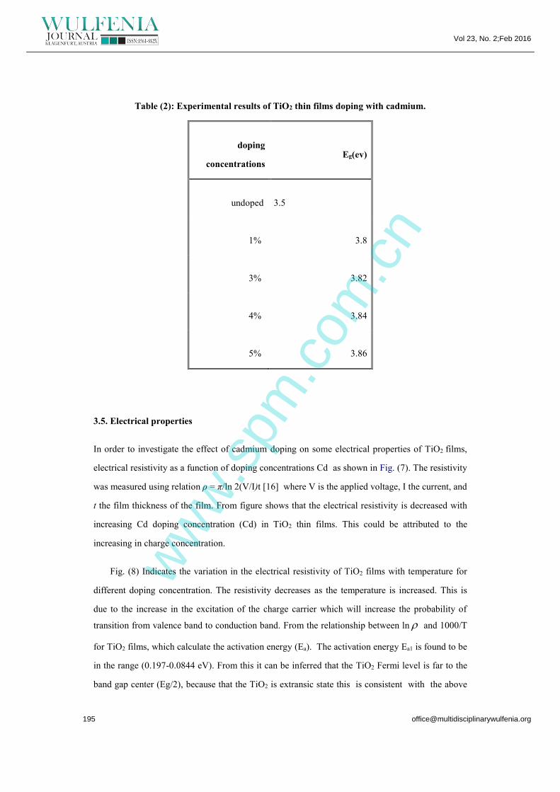
[4]. The optical band gap values for different parameters are tabulated in Table (2).
Fig. ( 6) :(A) (αhυ)2 verses hυ of TiO2 pure and doping with cadmium. (B) optical energy gap
as a function of different doping concentrations.(C) Plot of ΔEg against inverse square of the
grain radius (1/R2) of the TiO2 films of different doping concentrations.
0
2E+11
4E+11
6E+11
8E+11
1E+12
1.2E+12
1.4E+12
1.6E+12
1.8E+12
1 2 3 4 5
hn (eV)
(hn
)2 (
eV
/cm
)2
1% Cd
3% Cd
4% Cd
5% Cd
3.79
3.8
3.813.82
3.83
3.84
3.853.86
3.87
0 1 2 3 4 5 6
Doping concentration(%)
En
erg
y g
ap
(eV
)
B
0.29
0.3
0.31
0.32
0.33
0.34
0.35
0.36
0.37
0 0.2 0.4 0.6 0.8
1/R2 (nm)
-2
DE
g (e
V)
C
A
www.spm.co
m.cn
Vol 23, No. 2;Feb 2016
Table (2): Experimental results of TiO2 thin films doping with cadmium.
doping
concentrations (ev)gE
undoped 3.5
1% 3.8
3% 3.82
4% 3.84
5% 3.86
3.5. Electrical properties
In order to investigate the effect of cadmium doping on some electrical properties of TiO2 films,
electrical resistivity as a function of doping concentrations Cd as shown in Fig. (7). The resistivity
was measured using relation ρ = π/ln 2(V/I)t [16] where V is the applied voltage, I the current, and
t the film thickness of the film. From figure shows that the electrical resistivity is decreased with
increasing Cd doping concentration (Cd) in TiO2 thin films. This could be attributed to the
increasing in charge concentration.
Fig. (8) Indicates the variation in the electrical resistivity of TiO2 films with temperature for
different doping concentration. The resistivity decreases as the temperature is increased. This is
due to the increase in the excitation of the charge carrier which will increase the probability of
transition from valence band to conduction band. From the relationship between ln and 1000/T
for TiO2 films, which calculate the activation energy (Ea). The activation energy Ea1 is found to be
in the range (0.197-0.0844 eV). From this it can be inferred that the TiO2 Fermi level is far to the
band gap center (Eg/2), because that the TiO2 is extransic state this is consistent with the above
www.spm.co
m.cn

Vol 23, No. 2;Feb 2016
results for the electrical resistivity, also these values of activation energy are in agreement with the
previous works [2] . Table (3) shows the activation energy Ea1 and Ea2 of the TiO2 thin films doped
with cadmium.
different doping concentrations. at 2 for TiO 2and Ea 1ivation energies Ea) : Act3Table (
Doping with cadmium )V(ea1E )V(ea2E
undoped 0.0502 0.0526
1% 0.1972 0.1301
23% 0.1597 0.0726
4% 0.1263 0.1290
5% 0.0844 1.2034
3.6. Photocatalytic activity
The photocatalytic reaction is very sensitive to the catalyst surface. The reaction is initiated by the
production of electron hole pair on TiO2 surface which results from the absorption of photon with
Fig. (7): The electrical resistivity as a function of different Cd doping
. films 2for TiOconcentration
Fig. ( 8): Ln ρ as a function of 1000/T(K) doping Cd films at different2 TiO for 1-
.films 2for TiOconcentrations
0.0E+00
1.0E+03
2.0E+03
3.0E+03
4.0E+03
5.0E+03
6.0E+03
7.0E+03
0 1 2 3 4 5 6
doping concentration(%)
ρ(Ω
cm)
13.8
14
14.2
14.4
14.6
14.8
15
2.9 3 3.1 3.2 3.3
1000/T(kˉ¹)
Lnρ
1% Cd
3% Cd
4% Cd
5% Cd
www.spm.co
m.cn

Vol 23, No. 2;Feb 2016
energy equal or greater than the band gap. The MB reacts with electrons generated on the TiO2
particles under UV irradiation. Fig. 9 shows the absorbance of MB at 605 nm as a function of UV
light irradiation time on the TiO2 films immersed in the solution. The absorbance spectra of the
MB (100 mg/l) solution degraded with the TiO2 film which is shown in the inset of Fig. 9. In order
to demonstrate the degradation process, the spectra was recorded at different time intervals. The
experiment was repeated with two sets of films at identical conditions and the results were
reproducible. From Fig. 9 it can be observed that the absorbance decreases with light irradiation
time, which indicates the photodegradation of MB. Further it can be observed that the rate of
decrease in absorbance is significant in the case of films at high doping concentration. The
diminishing of the absorbance band at 605 nm is very noticeable indicating good photocatalytic
activity. The photocatalytic experiments show that the photocatalytic activity of Cd-doped TiO2
thin films has been enhanced compared with that of undoped TiO2 thin films. This enhancement
should be attributed to the increase of specific surface area [25].
Fig. 9. Absorbance at 605 nm of an aqueous methylene blue solution (MB) as a function of
UV light irradiation time of the TiO2 films immersed in it. Inset: absorption spectra of
aqueous MB solution (100 mg/l) degraded by a TiO2 film at doping concentration 5%.
4. Conclusions
Titanium oxide thin films were prepared by spray pyrolysis technique on quartz substrate at 623 K.
the effect of Cd doping on structure, electrical, optical, and photpcatalytic properties of TiO2 thin
films were studied by XRD, AFM, SEM, four probe and UV- Visible measurements. The major
observations of this study can be summarized as follows. The grain size showed dependence on
00.5
11.5
22.5
33.5
44.5
0 50 100 150 200 250 300
Irradiation time (min)
Ab
so
rba
nc
e (
a.u
)
1%3%4%5%
0
2
4
6
8
10
12
200 400 600 800 1000
l (nm)
Ab
so
rban
ce (
a.u
.)
www.spm.co
m.cn

Vol 23, No. 2;Feb 2016
doping concentration, the XRD results reveal that the deposited thin film of TiO2 has anatase
structure. Band gap of the film increased from 3.5 to 3.86 eV after doping, which is higher than the
values, reported in the literature. Atomic force microscope (AFM) results show that the addition of
the Cd to TiO2 thin films become smooth. The high band gap observed in this study can be
correlated with the nanocrystalline nature of the films (effect of quantum confinement).The effect
of doping the TiO2 film may enhance the photoresponse and can have positive results on the
photocatalytic activity.
5. References
[1] Diana Mardare , Felicia Iacomi, Nicoleta Cornei, Mihaela Girtan and Dumitru Luca "Undoped
and Cr-doped TiO2 thin films obtained by spray pyrolysis",Thin Solid Films 518 ,(2010) , 4586–
4589.
[2] I. Oja , A. Mere , M. Krunks , R. Nisumaa , C.-H. Solterbeck and M. Es-Souni "Structural and
electrical characterization of TiO2 films grown by spray pyrolysis" Thin Solid Films 515,
(2005),674-677 .
[3] L. Andronic, S. Manolache and A. Duta"TiO2 thin films prepared by spray pyrolysis deposition(SPD)
and their photocatalytic activities" , Journal Of Optoelectronics and Advanced Materials 9, (2007),1403 –
1406.
[4] N.R. Mathews, Erik R. Morales , M.A. Corte´s-Jacome and J.A. Toledo Antonio" TiO2 thin
films – Influence of annealing temperature on structural, optical and photocatalytic properties"
Solar Energy 83,(2009) ,1499–1508.
[5] T Maiyalagan, B Viswanathan, and U V Varadaraju,"fabrication and characterization of
uniform TiO2 nanotube arrays by sol-gel template method", Bull. Mater. Sci. 29, (2006),705-708,.
[6] K.K. Saini, Sunil Dutta Sharma, Chanderkant, Meenakshi Kar, Davinder Singh, C.P. Sharma,"
structural and optical properties of TiO2 thin films derived by sol-gel dip coating process", Journal
of Nano-Crystalline Solid 353, (2007) , 2469-2473.
[7] Tae-Sik Kang, Adam P. Smith, Barney E. Taylor, and Michael F. Durstock, "fabrication of
highly-ordered TiO2 nanotube arrays and their use in dye-sensitized silar cells", Nano Letters 9,
(2009), 601-606.
www.spm.co
m.cn

Vol 23, No. 2;Feb 2016
[8] Z. Can,D. Wanyu, W.Hualin, C.Weiping and J. Dongying "Influences of working pressure on
properties for TiO2 films deposited by DC pulse magnetron sputtering", Journal of Environmental
Sciences 21, (2009) ,741–744,.
[9] Yue-Kun Lai, Jian-Ying Huang, Hui-Fang Zhang, Vishnu-Priya Subramaniam, Yu-Xin Tang,
"nitrogen-doped TiO2 nanotube array films with enhanced photocatalytic activity under various
light sources", Journal of Hazardous Materials 184, (2010),855-863,.
[10] Yuxin Tang, Jie Tao, Zhili Dong, Joo Tien Oh, and Zhong Chen,"the formation of
micrometer-long TiO2 nanotube arrays by anodization of titanium film on conducting glass
substrate", Advanced in Natural Nanoscience and Nanotechnology 2, (2011),1-7.
[11] Lu-Lin Li, Chiau-Yiag Tsai, Hui-Ping Wu, Chien-Chon Chen , and Eric Wei-Guang Diau,
"morphologic characterization of anodic titania nanotube arrays for dye-sensitized solar cells,
Journal of the Chinese Chemical Society 27, (2010),1147-1150,.
[12]Hao Feng Lu, Feng Li, Gang Liu, Zhi-Gang Chen, Da-Wei Wang, Hai-Tao Fang, Gao Qing
Lu, Zhou Hua Jiang, and Hui-Ming Cheng," amorphous TiO2 nanotube arrays for low-temperature
oxygen sensors", Nanotechnology 19, (2008),1-7.
[13] Lu-Lin Li, Chiau-Yiag Tsai, Hui-Ping Wu, Chien-Chon Chen, and Eric Wei-Guang Diau,"
fabrication of long TiO2 nanotube arrays in a short time using a hybrid anodic method for highly
efficient dye-sensitized solar cells", Journal of Materials Chemistry 20, (2010), 2753-2758.
[14] Yuekun Lai, Huifang Zhuang, Lan Sun, Zhong Chen, and Changjian Lin, "self-organized
TiO2 nanotubes in mixed organic-inorganic electrolytes and their photoelectrochemical
performance", Electrochimica Acta 54, (2009), 6536-6542.
[15] Mona P. Moreta, Richard Zallena, Dilip P. Vijayb,1, Seshu B. Desub," Brookite-rich titania
lms made by pulsed laser deposition",Thin Solid Films 366, (2000), 8-10.
[16] H.P. Deshmukh, P.S. Shinde and P.S. Patil" Structural, optical and electrical characterization
of spray-deposited TiO2 thin films" Materials Science and Engineering B 130 , (2006), 220–227.
[17] L. Castañeda"Physical characterization of Titanium Dioxide thin films nanostructures
deposited by ultrasonic spray pyrolysis"Tecnólog 3, ( 2010).
www.spm.co
m.cn

Vol 23, No. 2;Feb 2016
[18] I . Oja, A. Mere , M. Krunks, C-H. Solterbeck and M. Es-Souni"Properties of TiO2 films
prepared by the spray pyrolysis method" Solid State Phenomena 99-100, (2004), 259-264.
[19] Sergiu T. Shishiyanu, Teodor S. Shishiyanu and Oleg I. Lupan " Sensing characteristics of
tin-doped ZnO thin films as NO2 gas sensor " Sensors and Actuators B 107, (2005), 379–386.
[20] S. Pawar, M. Chougule, P. Godse, D. Jundale, S. Pawar, B. Raut and V. Patil " Effect of
annealing on structural, morphological, electrical and optical properties of nanocrystalline TiO2
thin films", J. Nano- Electron. Phys. ,No.1, PP.185-192, (2011) ,from Iraq Virtual Science Library.
[21] I. Vaiciulis, M. Girtan, A. stanculescu, L. Leontie, F. Habelhames and S.Antohe"On Titanium
Dioxide spray deposited thin films for soler cells applications",Proceedings of the Romaniaan
Academy, Vol. 13, No. 4,(2012).
[22] S.G. Pawar, M.A. Chougule, P.R. Godse, D.M. Jundale, S.A. Pawar,B.T. Raut, and V.B.
Patil," Effect of annealing on structure, morphology, electrical and optical properties of
nanocrystalline TiO2 thin films", J. Nano- Electron. Phys., Vol. 3, No. 1, PP. 185-192, ( 2011) .
[23] M.Mohammadi,N.Shahtahmasebi, M. Karimipour, and R. Sarhaddi"Characterization of
nanostructured Nd-Doped TiO2 thin film synthesized by spray pyrolysis method: structural,
optical and magneto-optical properties", Indian Journal of Science and Technology, Vol. 5 ,No. 6
,( 2012) .
[24] Raid A. Ismail, Selma M. H. Al-Jawad and Naba Hussein," Preparation of n ZnO/p-Si solar
cells by oxidation of zinc nanoparticles: effect of oxidation temperature on the photovoltaic
properties",Applied Physics A materials science and processing, Vol.117, PP. 1977–1984, (2014).
[25] Gaige Zheng, WenjuanShang,LinhuaXu, ShanGuo, and ZihaoZhou'' Enhanced photocatalytic
activity of ZnO thin films deriving from a porous structure", Materials Letters, Vol. 150 , PP. 1-4,
( 2015) .
All in-text references underlined in blue are linked to publications on ResearchGate, letting you access and read them immediately.
www.spm.co
m.cn