Virtual University of Pakistan · The Currents of a BJT - DC biasing-BJT - Forward bias of Base...
246
Circuit Theory (PHY 301) Lecture Handouts By Professor Dr. Tajamul Hussain Virtual University of Pakistan
Transcript of Virtual University of Pakistan · The Currents of a BJT - DC biasing-BJT - Forward bias of Base...

Circuit Theory (PHY 301)
Lecture Handouts By
Professor Dr. Tajamul Hussain
Virtual University of Pakistan

Course contents
Lecture No. Topic/Sub topic Page No.
1
International System of Units - Basic Units - Decimal System - Sub-atomic elements - Electrons and protons in an Atom - Structure of the Atom - Electron Valence - Sub-shells - Particles in the Nucleus - Atomic Number - Orbital Rings - Conductors - Insulators - Semiconductors - The Unit of Electric Charge - Negative and Positive Polarities
1
2
Negative and Positive Polarities of battery - Potential difference - Potential between different charges - Potential difference between the terminals - Volt - Current - Potential difference is necessary for current - Ampere - Resistance - Ohm - Conductance - The closed circuit - Open circuit - Short circuit - Power - Passive sign conventions
14
3 Resistance in Series 21
4
Inductance - Inductance in Series - Inductance in Parallel - Capacitance - Capacitance in parallel - Capacitance in Series - Ohm's Law - The Current “I=V/R” - High Voltage but Low Current - Low Voltage but High Current - The Voltage V=IR - The Resistance R=V/I - The Linear Proportion Between V & I - Volt-Ampere Characteristics - Power Dissipation in Resistance
29
5
Types of sources : Ideal voltage source - Ideal current source - Direct voltage - Direct quantities - Alternating quantities - Dependent or controlled sources - Voltage controlled voltage source - Current controlled voltage source - Voltage Controlled Current Source - Current Controlled Current Source - Voltage dividers and Current dividers - Series Voltage dividers
37
6 Current divider with two parallel resistances - 46
7 Kirchhoff's Laws Kirchhoff's Current Law (KCL) - Node - Branch - Loop - Ground - 54
8 Application of Nodal Analysis 609 Application of Nodal Analysis - Refrence node 65
10 Super Node - Constraint or Coupling Equation - Examples of Nodal Analysis 72
11 Examples of Nodal Analysis - Super Node technique 7612 Kirchhoff's Voltage Law (KVL) - Loop - Examples of Loop Analysis 8013 Applications of Loop Analysis 8214 Applications of Loop Analysis 8415 Applications of Loop Analysis 8716 Applications of Loop Analysis 9017 Applications of Loop Analysis 9618 Applications of Loop Analysis - Super Mesh Technique 9919 Examples of Loop Analysis 105
20 Applications of Loop Analysis - Super Mesh Technique - Coupling equation 108
21 Examples of Loop Analysis by using dependent sources - Coupling equation 112
22 Matrices and determinants 11523 Superposition Theorem and examples 11924 Source Transformation and examples 12425 Thevenin's Theorem and examples 130
26 Examples of Thevenin's Theorem - Thevenin's Theorem and Dependent sources with examples 136

27 Thevenin's Theorem and Dependent sources with examples - Norton's Theorem with examples 143
28 Norton's Theorem with examples - Linearity Principle 150
29 Intrinsic Silicon - Drift - Diffusion - Diffusion Current - Drift Current - Drift Velocity - Doped semiconductors - Diffusion current ID - The depletion region - The PN Junction under reverse bias and forwar biased conditions -
156
30 PN Junction Diode - Ideal Diode - Ideal Diode as a Rectifier 15931 Terminal characteristics of the Junction diodes - Forward bias region 16232 Reverse bias region - Break down region - Analysis of diode circuits 166
33 DC or Static Resistance - The constant voltage drop model - AC or Dynamic Resistnace 170
34 Small Signal Model and its applications 174
35 Transformers - Secondary voltage and current - Transformer Input/Output phase rlationship 180
36 Negative Half Wave Rectifiers - Load voltage and current - Average Load voltage and current - 184
37 Peak Inverse Voltage (PIV) - Full wave rectifier 18938 Negative full wave rectifier - Full wave bridge rectifier - 19339 Filters - Clippers - Series clippers - 19840 Parallel clippers - Clamper 206
41 Diode logic gates (OR Gate) ( AND Gate) - Voltage multipliers - Half wave voltage doubler - Zener diode - Zener diode shunt regulator 212
42 Applications of Zener diode shunt regulator - Characteristic of light emitting diodes - PIN Photodiodes - Tunnel diode 218
43 Bipolar Junction Transistor (BJT) - NPN Transistor - Operating configuration of BJT - Directions of Currents in BJT - Modes of operation of BJT
223
44 The Currents of a BJT - DC biasing-BJT - Forward bias of Base Emitter - Load line analysis - DC BIASING-BJT Emitter-Stabilized Bias Circuit - Base Emitter Loop - Collector Emitter Loop
229
45 Emitter-Stabilized Bias Circuit Load Line Analysis - DC BIASING-BJT Voltage Divider Bias Circuit and its application 237

Circuit Theory (Phy301) VU
Page 1 of 243
© Copyright Virtual University of Pakistan
LECTURE 1
(Introduction-some basic concepts) International System of Units
It is built upon seven basic units.These are meter, kilogram, second, ampere, Kelvin, mole and candela.
Basic Units The seven quantities are known to be basic in SI unit System.
Base quantity Name symbol
Length meter m
Mass kilogram kg
Time second s
Electric current ampere A
Thermodynamic temperature
Kelvin K
Amount of substance mole mol
Luminous intensity candela cd
Meter Up until 1983, the meter was defined as 1,650,763.73 wavelengths in a vacuum of the orange-red line of the spectrum of krypton-86. Since then, it is equal to the distance traveled by light in vacuum in 1/299,792,45 of a second. Second The second is defined as the duration of 9,192,631,770 cycles of the radiation associated with a specified transition of the Cesium-133 atom. Kilogram The standard for the kilogram is a cylinder of platinum-iridium alloy kept by International Bureau of Weights and Measures at Paris. The kilogram is the only base unit still defined by a physical object. Kelvin The Kelvin is defined as the fraction 1/273.16 of the thermodynamic temperature of the triple point of water, that is, the point at which water forms an interface of the solid, liquid and vapor. This is defined as .01oC on the Centigrade scale and 32.02oF on Fahrenheit scale. The temperature 0oK is called the “absolute zero”.

Circuit Theory (Phy301) VU
Page 2 of 243
© Copyright Virtual University of Pakistan
Ampere The Ampere is defined as that current, if maintained in each of two long parallel wires separated by a distance of one meter, would produce a force, between the two wires, of 2 x 10⁻⁷ Newton, for each meter of length. Candela The Candela is defined as the luminous intensity of 1/600,000 of a square meter of a cavity at a temperature of freezing platinum (2,042 ok). Mole The mole is defined as the amount of substance of a system that contains as many elementary entities as there are as many atoms in 0.012 kilogram of the Carbon-12. Joule Joule is defined as the energy consumed in moving an object of one kg through a distance of one meter.One joule is equivalent to the 0.7376 foot pound-force and .2388 calories. Watt Watt is defined as the “Rate of doing work.” One watt =1 joule/second One watt is equivalent to 0.7376 ft--lbf/s or equivalently 1/745.7 horsepower. Decimal System The SI system uses the decimal system to relate larger and smaller units to basic units. It employs prefixes to signify the various power of 10. Decimal System (Prefixes)
Factor Name Symbol Factor Name Symbol 10-24 yocto y 1024 yotta Y
10-21 zepto z 1021 zetta Z
10-18 atto a 1018 exa E
10-15 femto f 1015 peta P
10-12 pico p 1012 tera T
10-9 nano n 109 giga G
10-6 micro µ 106 mega M
10-3 milli m 103 kilo k
10-2 centi c 102 hecto h
10-1 deci d 101 Deka da

Circuit Theory (Phy301) VU
Page 3 of 243
© Copyright Virtual University of Pakistan
Example 1 A laser emits light at a wavelength of 248nm. This is same as (a) .0248 millimeter. Or (b) 2.48 micrometer. Or (c) 0.248 micrometer. Or (d) 24800 angstrom. Answer (c) 0.248 micrometer. Example 2 A logic gate switches from the on state to the off state in 10 neno seconds, this corresponds to (a)0.1 micro second or (b)10 micro second or (c) .001 micro second or (d) .01 micro second Answer (d) .01 micro second Sub-atomic elements Electron: It is a negatively charged particle. Proton: It is a positively charged particle. Neutron: It is a neutral particle and carries no charge. Electrons and protons in an Atom An atom is the smallest particle of the basic elements which form the physical substance we know as solid, liquid and gas. Each stable combination of electrons and protons make one particular type of atom. To understand the concepts of electronics we must have the understanding what is happening at the atomic level, not why it happens. There are number of methods by which electrons and protons might be grouped. They assemble in specific atomic combination for a stable arrangement. As a result, the electron stays in its orbit around the nucleus. In an atom that have more electrons and protons than hydrogen atom, all the protons are in nucleus, while all the electrons are in one or more ings around the nucleus. The proton in the nucleus makes it heavier and stable part of the atom because it Is 1840 times heavier than the electron.

Circuit Theory (Phy301) VU
Page 4 of 243
© Copyright Virtual University of Pakistan
One electron is shown as the orbital ring around the nucleus. In order to account for the atom’s stability we can consider electron spinning around the nucleus as planets revolve around the sun. The electrical force attracting the electron towards proton is balanced by the mechanical force (centrifugal force) directing it outwards. The total number of electrons in the outer rings must equal to the number of protons in the nucleus in a neutral atom. The distribution of electrons in the orbital ring determines the atoms electrical stability. Especially important are the number of electrons farthest from the nucleus. For example carbon atom illustrated in the figure, 6 protons in the nucleus and 6 electrons in two outside rings.
This outermost ring requires 8 electrons stability, except, when there is only one ring which require only 2 electrons for its stability.

Circuit Theory (Phy301) VU
Page 5 of 243
© Copyright Virtual University of Pakistan
As another example, the copper atom in figure below has only one electron in the last ring which can include 8 electrons. Therefore the outside ring of copper is less stable than carbon.
When there are many atoms closed in a copper wire, the outermost electrons are not sure from which atom they belong to. They can migrate easily from one atom to another at random. These electrons are called “free electrons”. Structure of the Atom Although no body has ever seen an atom, its hypothetical structure fits experimental evidence that has been measured very exactly. The size and electrical charge of the invisible particles are indicated by how much they are affected by the known forces. Our present planetary model of the atom is proposed by Neil Bohar in 1913.His contribution was joined with the new ideas of nuclear atom developed by Lord Ruther Ford. With the quantum theory developed by Max Plank and Albert Einstein. The nucleus contains protons for all the positive charge in the atom. The number of protons in the nucleus is equal to the number of planetary electrons. The positive and negative charges are as the electrons and protons have the equal and opposite charges. The orbits for the planetary electrons are also called shells or energy levels. Electron Valence This value is the number of electrons in an incomplete outermost shell. A completed outer shell has a valence of zero. Copper for instance, has a Valence of 1, as there is one electron in the outermost shell of the copper Atom.

Circuit Theory (Phy301) VU
Page 6 of 243
© Copyright Virtual University of Pakistan
Sub-shells Although not shown in the illustrations, all the shells except K shell are divided into sub-shells. This sub-division accounts for the different types of the orbits in the same shell. For instance, electrons in the one sub-shell will have circular orbits while other electrons of the same shell will have elliptical orbit. This sub-division accounts for the magnetic properties of the atom. Particles in the Nucleus A stable nucleus, it is not radioactive, but contains protons and neutrons.The neutron is electrically neutral particle, without any charge.Its mass is almost same as that of proton.The proton has the positive charge of the hydrogen nucleus.Table lists the charge and mass for these three basic particles in all atoms.
STABLE PARTICLES IN THE ATOM
Particle Charge Mass
Electrons in orbital shells
0.16x10⁻¹⁸C, negative
9.108x10⁻²⁸ g
Proton in nucleus
0.16x10⁻¹⁸C, positive
1.672x10⁻²⁴ g
Neutron, in nucleus
None 1.675x10⁻²⁴ g
Atomic Number This gives the number of protons or electrons required in the atom of an element. Hydrogen atom has atomic number 1. Orbital Rings The planetary electrons in successive shells are called K, L, M, N, O, P and Q at increasing distance outward from the nucleus. Each shell has a maximum number of electrons for stability. As indicated in Table these stable shells correspond to the inert gases as helium and neon etc.
SHELLS OR ORBITAL ELECTRONS IN THE ATOM SHELL MAXIMUM ELECTRONS INERT
GAS K 2 Helium
L 8 Neon
For example electronic configuration of the copper atom having 29 protons in nucleus and 29 orbital electrons will be

Circuit Theory (Phy301) VU
Page 7 of 243
© Copyright Virtual University of Pakistan
K shell = 2 electrons L shell = 8 electrons M shell =18 electrons N shell =1 electron Total = 29 electrons Example 1 An element with 16 protons and 16 electrons has atomic number value (a) 14 Or (b) 18 Or (c) 16 Or (d) 22 Answer (c) 16 Example 2 What is the electron valence of an element of atomic number 5 (a) 2 Or (b) 3 Or (c) 4 Or (d) 5 Answer (b) 3 Conductors When electrons can move easily from one atom to another in a material, it is a conductor. In general all the metals are good conductors, with silver the best and copper at second. Insulators A material with atoms in which the electrons tend to stay in their own orbits is an insulator and it cannot conduct electricity easily. However, the insulators are able to hold or store electricity better than the conductors. These are also called dielectric materials. Semiconductors Carbon can be considered as semiconductor, conducting less than the metal conductors but more than the insulators. In the same group are germanium and silicon which are commonly used for transistor and other semiconductor components. Coulomb: The Unit of Electric Charge The mechanical force of attraction and repulsion between the charges is the fundamental method by which electricity makes itself evident. Any charge is an example of static electricity because the electrons and protons are not in motion.

Circuit Theory (Phy301) VU
Page 8 of 243
© Copyright Virtual University of Pakistan
The charge of many billions of electrons or protons is necessary for common applications of electricity. Therefore, it is convenient to define a practical unit called coulomb(C) as equal to charge of 6.25 x 10 18 electrons or protons stored in a dielectric. The analysis of static charges and their forces is called electrostatics. The symbol of electric charge is Q or q, standing for quantity. This unit is named after Charles A. Coulomb, a French physicist, who measured force between the charges. Negative and Positive Polarities Historically, the negative polarity refers to as static charge produced on rubber, amber, silk and resinous material in general. Positive polarity refers to the static charge produced on glass and other various materials. On the basis of this, the electrons in all atoms are basic particles of negative charge because their polarity is same as the charge on rubber. Protons have positive charge because the polarity is same as the charge on glass. Charges of the Same Polarity Repel Exercises (1) What will be the atomic number of an atom having 29 electrons? (2) Charge of 1 coulomb and charge of -2 coulomb will attract or repel? (3) What will be the electronic distribution of an atom of atomic number 23? The Atom Atoms, the fundamental building blocks of matter, are made of three kinds of particles: electrons: negatively charged: electrons orbit the nucleus protons: positively charged: part of the nucleus neutrons: neutrally charged: part of the nucleus

Circuit Theory (Phy301) VU
Page 9 of 243
© Copyright Virtual University of Pakistan
The figure above shows a particularly simple atom (an "isotope" of hydrogen, called deuterium, which just happens to have one particle of each type). All atoms except hydrogen atoms have more than one electron, proton, and usually one or more neutrons. Electron's orbit around the nucleus, which lies at the center and contains the protons and neutrons. The electron stays in orbit because it is negatively charged, and is therefore attracted to the positively charged proton in the nucleus. This is an example of the Law of electrical charges: Like charges repel, opposite charges attract. Most atoms, when in their normal state as components of matter, have the same number of electrons as protons, so that the total, or net charge of the atom is zero. That is, the atom is neutral. The number of protons (which is equal to the number of electrons if the atom is neutral) is called the atomic number of the atom, and this determines what element (hydrogen, helium, iron, etc), that the atom is classified as. Ions are atoms to which some electrons have been added or taken away, so that the atom has a net charge (positive if electrons have been removed, negative if electrons have been added). Ions that have opposite net charges attract, and those with net charges of the same sign repel. Atoms of the same atomic number can have different numbers of neutrons. These are the different isotopes of an element. Hydrogen has three isotopes: no neutrons - called "protium" (this is the hydrogen isotope most commonly found), one neutron - called deuterium, and two neutrons - called tritium. Although he didn't know about electrons and protons, the designations of positive and negative were made by Benjamin Franklin over two hundred years ago! Later on people realized they corresponded to the charges of protons and electrons, respectively. What is Electricity? In some materials, particularly metals, the electrons farthest from the nucleus are not bound to a particular atom - they can move freely from one atom to another. Electricity is the flow of these free electrons in a wire:

Circuit Theory (Phy301) VU
Page 10 of 243
© Copyright Virtual University of Pakistan
Such a flow of electrons is called a current. What makes these free electrons move? Suppose we put something that has a net positive charge at the one end of the wire (say, at the right end of the wire pictured above). Let's also suppose that we put something with a net negative charge at the other end (the left end in the wire above). Then the electrons in the wire will be attracted to the positive end and repelled by the negative end. Hence, they will flow from left to right. That's electricity! Batteries Batteries are devices which can do exactly what is described just above - make a current flow by creating a positive charge at one end of a wire and a negative charge at the other. A battery has two terminals (wire contacts), called positive and negative, corresponding to the net charges created at the terminals. The symbol for a battery is the following:
When a wire is connected across these terminals, forming a closed circuit, the positive and negative charges created by the battery cause a current to flow:
Note that the electrons flow from the negative terminal to the positive terminal. Eventually, when enough electrons have flowed, the battery will become drained, and the current will cease. Even though the electrons flow from the negative to the positive terminals, it is conventional to say that the current flows from positive to negative:

Circuit Theory (Phy301) VU
Page 11 of 243
© Copyright Virtual University of Pakistan
Why is this? This is simply because people can't see electrons, and so they guessed wrong when the settled on a convention. But this is not really a problem, because even today we still don't see electrons in most applications, so it doesn't really matter for most purposes which direction the electrons actually go. Measuring Current How do we measure current? Current is measured by literally counting the number of electrons that pass a given point in the wire. Any point will do - it doesn't matter which one because the current will be the same in each point of the wire, unless the wire branches off into a more complicated circuit. Because there are billions of billions (much more than billions and billions! Carl Sagan would be impressed!) of electrons in even a very little piece of wire, we need to have a unit of measurement that will make it easy to count so many. The basic unit for counting electrons (that is, charge) is the "coulomb" (pronounced "cool lum"): 1 coulomb = 1.6 x 10¹⁹ electrons = 16,000,000,000,000,000,000 = 16 billion billion electrons! To measure current, we pick one point along the wire and count the electrons that go by, like watching things go by on an assembly line. If 1 coulomb of electrons go by each second, then we say that the current is 1 "ampere" (pronounced "am - peer"), or 1 amp for short. If 2 coulomb's per second goes by, we say the current is 2 amps, and so on: 1 ampere = 1 coulomb per second It is traditional to represent the current with the symbol I, as in I = 1 amperes, or I = 15 amperes, etc. Measuring Voltage Some batteries try to push electrons through the wire more strongly than others. How strongly the battery pushes is a measure of its voltage, symbolized with the letter V (as in the diagrams above). You can think of voltage like pressure: the higher the voltage, the higher the pressure is to push electrons through the wire. The lower the voltage, the lower the pressure. Voltage is measured in volts. For example, common voltages for batteries are 1.5 volts, 6 volts, 9 volts, and 12 volts. Car batteries are typically 12 volts. An electrical outlet in the United States has a voltage of 110 volts (pretty high!). The voltage of a battery is related to the amount of energy that the battery can deliver. A voltage of V = 1 volt means that the battery will deliver 1 "Joule" of energy for each coulomb of charge that flows through the circuit. A voltage of V = 2 means that the battery will deliver 2 Joules of energy for each coulomb. A Joule is the basic unit of energy in the metric International system of units - its about the amount of energy it takes to lift two pounds 9 inches. How high the voltage of the battery is depends in detail on the internal construction of the battery, which is an "electro-chemical" energy storage device.

Circuit Theory (Phy301) VU
Page 12 of 243
© Copyright Virtual University of Pakistan
Measuring Resistance How are amperes (current) and voltage (electrical pressure), related to one another? For a given voltage, some wires let more current flow than others. A wire that doesn't let very much current flow is said to have high resistance. Resistance is symbolized with the letter R. To simplify matters, we usually assume that the wire itself is an ideal wire with no resistance, and we represent the resistance as a localized component of the circuit symbolized with a broken line:
In fact the resistor now can represent the sum total of the wire's resistance, including that contributed by any additional components in the circuit that have resistance. There are devices call "resistors" whose function is simply to provide additional resistance. The resistance is related to how much the current I we get from a given applied voltage V by "Ohm's Law" in the following way: Ohm's Law: I = V / R If I is measured in amperes, and V in volts, then we say that R has units of "ohms" (pronounced "olms"). More specifically, if we have a 1 volt battery, and a wire with a resistance of 1 ohm, then the current that results when the wire is placed across the battery's terminals is given by I = V / R = 1 volt / 1 ohm = 1 ampere. Likewise, if we have a 2 volt battery, and a wire with a resistance of 3 ohms, then the current that results when the wire is placed across the battery's terminals is given by I = V / R = 2 volt / 3 ohm = 2/3 amperes. Thus, knowing the voltage and the resistance, we can now predict the current. Likewise, we can also no turn the problem around, and say, calculate the resistance by measuring the voltage and current with a voltmeter (voltmeters are capable of measuring both voltage and current - but not generally at the same time!). Measuring Power in Watts What happens to the energy delivered to the wire? For the case of a simple piece of wire plus some additional devices with are purely resistive, the energy is completely converted into heat energy in the wire (as shown in the figure above), which escapes into space. As discussed above, the voltage of a battery is related to the amount of energy that the battery can deliver. A voltage of V = 1 volt means that the battery will deliver 1 Joule of energy for each coulomb of charge that flows through the circuit, a voltage of V = 2 yields two Joules per coulomb, and so forth. In many practical applications, we want to know the rate at which energy is delivered, not how much energy is delivered per coulomb of charge. For example, you might need to insure that a circuit you design will deliver 2 joules per second to make a toy car go fast enough. The rate at which energy is delivered is called power. Power is thus defined: Power = Energy / Time.

Circuit Theory (Phy301) VU
Page 13 of 243
© Copyright Virtual University of Pakistan
In the metric International units, the unit of power corresponding to 1 joule per second is called a watt: 1 watt = 1 joule per second. Because the voltage V tells us the number of joules per coulomb, and the current I tells us the number of coulombs per second, all we have to do to get the current is to multiply them: Power = number of watts = number of joules/second = joules/coulomb x coulombs/second = I V, Or Power Formula: P = I V Thus, suppose we had a circuit with a battery voltage of 2 volts and a current of 3 amps. Then the power delivered to the resistor would be P = I V = (3 amps) (2 volts) = 6 watts.

Circuit Theory (Phy301) VU
Page 14 of 243
© Copyright Virtual University of Pakistan
LECTURE 2
(Introduction-some basic concepts)
NEGATIVE AND POSITIVE POLARITIES OF BATTERY
We see the effects of electricity in a battery, static charge, lighting, radio, television, and many other applications. What do they all have common that is electrical in nature? The answer is basic particles of opposite polarity. As we studied in the last lecture, all the materials, including solids, liquids, and gases, contain two basic particles of electric charge: the electrons and protons. An electron is the smallest amount of electrical charge having characteristics called the negative polarity. The proton is a basic particle with positive polarity. In order to use the electrical forces associated with the negative and positive charges in all matter, some work must be done to separate the electrons and protons. Changing the balancing forces produces evidence of electricity. A battery for instance, can do electrical work because its chemical energy separates electric charges to produce an excess of negative charge at its negative terminal and an excess of protons on its positive terminal. With separate and opposite charges at the two terminals, electric energy can be supplied to a circuit connected to the battery. In fig below shows a battery with the negative (-) and positive (+) terminals marked to emphasize the two opposite polarities.
POTENTIAL DIFFERENCE Potential difference is actually the difference between the electric potentials at the two terminal of a circuit element.
Potential refers to the possibility of doing work. Any charge has the potential to do the work of moving another charge, by either attraction or repulsion. When we consider two unlike charges, they have a difference of potential. A charge is the result of work done in separating electrons and protons. The work of producing the charge causes a condition of stress in protons, which try to attract the
electrons and return to the neutral condition and vice versa.
POTENTIAL BETWEEN DIFFERENT CHARGES For instance, consider a positive charge of 3 C, shown in fig below.

Circuit Theory (Phy301) VU
Page 15 of 243
© Copyright Virtual University of Pakistan
The work to be done in moving some electrons, as illustrated. Assume a charge of 1C can move three electrons. In Fig a Then the charge of +3C can attract 9 electrons toward right. However, a charge of +1 C at the opposite side can attract 3 electrons towards left. The net result , then is that 6 electrons can be moved toward the right to the more positive charge. In Fig b , one charge is 2C ,while the other charge is neutral with 0C.For the difference of 2C ,again 2*3 or 6 electrons can be attracted to the positive side.
POTENTIAL DIFFERENCE BETWEEN THE TERMINALS
A voltage can exist between the terminals of a battery even a current is flowing or not. An automobile battery, for example, have 12 volts of voltage across its terminals if nothing whatsoever
is connected to the terminals. VOLTAGE CONVENTIONS
VOLT
This unit is named after Alessandro Volta. Fundamentally, the volt is the measure of the work needed to move an electric charge. When 0.7376
foot-pound of work is required to move 6.25x10¹⁸
electrons between two points, each with its own charge, the potential difference is one.
6.25x10¹⁸
electrons make up one coulomb. 0.7376 ft-lb of work is same as I joule, which is the practical unit of work or energy. So we can say that
1V=1J/1C The symbol of potential difference is V for voltage. In fact, the volt unit is used so often that potential difference is called voltage.
CURRENT When the potential difference between two charges forces a third charge to move, the charge in motion
is called current. To produce current, therefore, charge must be moved by a potential difference. In solid materials, such as copper wire, the free electrons are charges that can be forced to move with
relative ease by a potential difference, they are required a little work to be moved. As illustrated in fig. if a potential difference is connected across two ends of a copper wire the applied voltage forces the free electron to move.

Circuit Theory (Phy301) VU
Page 16 of 243
© Copyright Virtual University of Pakistan
This current is drift of electrons, from the point of negative charge at one end, and returning to the positive charge at the other end.
Each electron in the middle row is numbered, corresponding to a copper to which this electron belongs. Considering the case of only one electron moving, note that the electron returning to the positive side of
the voltage source is not electron S which left negative side. All electrons are same. Therefore, the drift free electrons resulted in the charge of one electron moving
through the wire. This charge in motion is current. Current is the constant flow of electrons. Only the electrons move, not the potential difference. The current must be the same at all points of the wire at all times.
Another definition of current can be made as Let q(t) be the total charge that has passed a reference point since an arbitrary time t=0, moving in the
defined direction. A contribution to this total charge will be negative if the negative charge is flowing in the reference direction.
As the figure shows a history of total charge q(t) that has passed a given reference point in a wire.
The current at a specific point and flowing in a specified direction as the instantaneous rate at which net
positive charge is moving past the point in the specified direction. Current is symbolized as I or i .
Mathematically it can be given as I = dq/dt GRAPHICAL SYMBOLS FOR CURRENT
POTENTIAL DIFFERENCE IS NECESSARY FOR CURRENT The number of free electrons that can be forced to drift through the wire to produce the moving charge
depends upon the amount of potential difference across the wire, with more applied voltage, the forces of attraction and repulsion can make more free electrons drift, producing more current.
With zero potential difference across the wire, there will be no current. As another case, connecting the same potential across the terminals of a wire will result in no current
flow. THE AMPERE OF CURRENT
Sine current is the movement of charge, the unit for stating the amount of currant is defined as the rate of flow charge.
Circuit Theory (Phy301) VU
Page 17 of 243
© Copyright Virtual University of Pakistan
When charge moves at the rate of 6.25x10
18 electrons flowing past a given point per second, the value
of current is one Ampere.
RESISTANCE
The fact that a wire conducting a current can become hot is evident that the work done by the applied voltage in producing current is due to accomplishment against some form of opposition.
This opposition, which limits the current , is called resistance. The atoms of a copper wire have a large number of free electrons, which can be moved easily by a
potential difference. Therefore, the copper wire has little opposition to the flow of free electrons when voltage is applied,
corresponding to low value of resistance. Carbon, however, has fewer free electrons than copper. When the same amount of voltage is applied to the carbon as to the copper ,fewer electrons will flow. Carbon opposes the current more than copper, therefore, has a higher value of resistance.
OHM
The practical unit of resistance is the ohm. A resistance that develops 0.24 calorie of heat when one ampere of current flows through it, for one
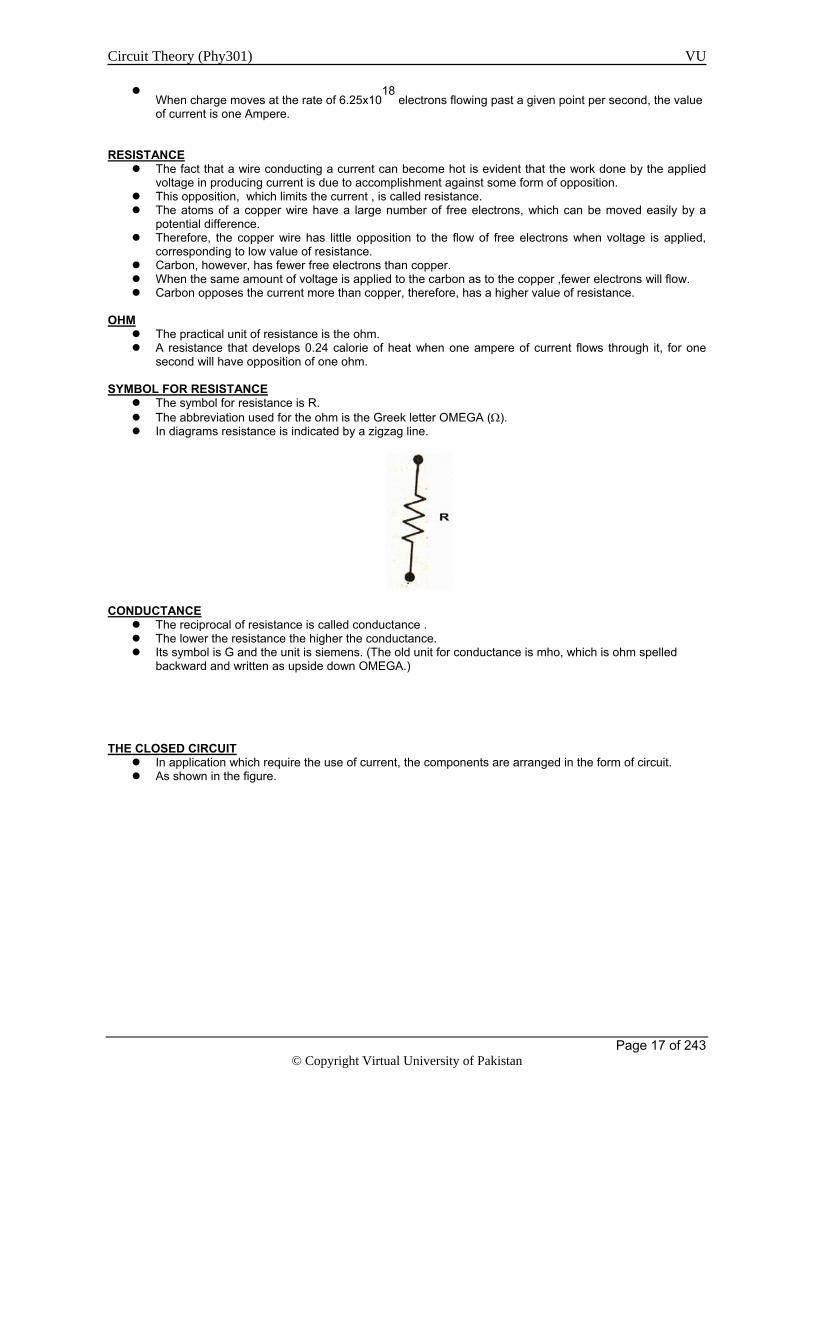
second will have opposition of one ohm. SYMBOL FOR RESISTANCE
The symbol for resistance is R. The abbreviation used for the ohm is the Greek letter OMEGA (Ω). In diagrams resistance is indicated by a zigzag line.
CONDUCTANCE
The reciprocal of resistance is called conductance . The lower the resistance the higher the conductance. Its symbol is G and the unit is siemens. (The old unit for conductance is mho, which is ohm spelled
backward and written as upside down OMEGA.) THE CLOSED CIRCUIT
In application which require the use of current, the components are arranged in the form of circuit. As shown in the figure.

Circuit Theory (Phy301) VU
Page 18 of 243
© Copyright Virtual University of Pakistan
For a closed circuit, these things should always keep in mind. (1) There must be a source of voltage. Without applied voltage current can not flow.
(2) There must be a complete path of current flow, from one side of the applied voltage source, through the external circuit, and returning to the other side of the voltage source. (3) The current path normally has resistance. The purpose of a resistance in the circuit is either generating heat or limiting the amount of current.
OPEN CIRCUIT When any part of the path is broken, the circuit is open because there is no continuity in the conducting
path. The resistance of an open circuit is infinitely high. The result in no current in the open circuit.
SHORT CIRCUIT
In this case, the voltage source has a closed path across its terminals, but the resistance is practically zero.
The result is too much current in the short circuit. Usually, the short circuit is a bypass across the load resistance.
POWER Rate of doing work is called power.
The unit of electric power is watt. One watt of power is equals the work done in one second by one volt of potential difference in moving
one coulomb of charge. We know that one coulomb per second is an ampere. Therefore power in watts equals the product of
volt times amperes. Power in watts = volts x amperes
P = V X I Dimensionally, the right side of this equation is the product of joules per coulomb and coulombs per second, which produces the expected dimension of joule per second or watt.
The sketch shows that if one terminal of the element is v volts positive with respect to the other terminal,
and of current i is entering the element through the terminal then the power is absorbed by the element. It is also correct to say that a power p =vi is being delivered to the element.
PASSIVE SIGN CONVENTIONS If the current arrow is directed into the + marked terminal of an element, then p=vi yields the absorbed
power.

Circuit Theory (Phy301) VU
Page 19 of 243
© Copyright Virtual University of Pakistan
A negative value indicates the power is actually being generated by the element, it might have been better to define a current flowing out of the + terminal.
Example Q. A simple circuit is formed using a12V lead-acid battery and an automobile headlight. If the battery delivers a total energy of 460.8watt-hours over an 8 hours discharge period.
(a) How much power is delivered to the headlight? (b) What is the current flowing through the bulb (assume the battery voltage remains constant while discharging)
Solution: The battery delivers energy of 460.8 W-hr over a period of 8 hrs.
(a) The power delivered to the headlight is therefore (460.8 W-hrs) (b) The current through the headlight is equal to the power it absorbs from the battery divided by the Voltage, at which the power is supplied, OR I = (57.6 W)/(12V) = 4.8 A
Importance of Earth Ground Voltage can not be defined at a single point it is by definition the difference in potential between two points. However, many schematics makes use of the conversion of taking the earth as defining zero volts, so that all other voltages are implicitly referenced to this potential. The concept is often referred to as earth ground, and is fundamentally tied to safety regulations designed to prevent fires, fatal electrical shocks, and related mayhem. The symbol for earth ground is shown in the figure below Since earth ground is defined as zero volts, it is often convenient to use this as a common terminal in schematics. The circuit of Fig a is shown redrawn in this fashion in Fig b. Where the earth ground symbol represents a common node. It is important to note that the two circuits are equivalent in terms of our value for Va.
Example The fact that the common terminal of a circuit may or may not be connected by some low-resistance pathway to earth ground can lead to potentially dangerous situations. Consider the diagram of Fig, which depicts an innocent bystander about to touch a piece of equipment powered by an ac outlet.
Only two terminals have been used from the wall socket; the round ground pin of the receptacles was left unconnected. The common terminal of every circuit in the equipment has been tied together and electrically connected to the conducting equipment chassis;

Circuit Theory (Phy301) VU
Page 20 of 243
© Copyright Virtual University of Pakistan
Chassis Ground This terminal is often denoted using the chassis ground symbol of Fig(a). The electrical connection to earth, however, has been made (inadvertently) a nonzero resistance; it may be the table for all we know. In any event, there is no reason to except this chassis ground to be the earth ground.
A pseudo-schematic (some liberty was taken with the person's equivalent resistance symbol) of the situation is shown in Fig. If the equivalent resistance of the person is significantly less than the resistance of all other possible paths to ground… well, let's just say not all stories have happy endings.
The fact that "ground" is not always "earth ground" can cause a wide range of safety and electrical noise problems.

Circuit Theory (Phy301) VU
Page 21 of 243
© Copyright Virtual University of Pakistan
LECTURE 3 (Resistance in Series) Resistance in Series
If we connect resistors across a source such that the ending point of one resistor is joined with starting point of the other resistor then they are said to be connected in series. The combined effect of all the resistors will be equal to the sum of individual resistances.
Consider two resistances R1 and R2 with terminals A, B and C, D as shown in the figure.
They will be in series if we connect B with C as shown in the figure
Combined effect of these two resistances will be Req = R1 +R2 Therefore, if we connect N resistances in series then R eq = R1+R2+R3 + - - - - - - - - -+ RN
To illustrate this effect we take some examples. Example 1 Simplify the given circuit.
Solution: So R
AB= R
1 +R
2 =1 k+ 1k= 2kΩ
Example 2 Simplify the given circuit.
Circuit Theory (Phy301) VU
Page 22 of 243
© Copyright Virtual University of Pakistan
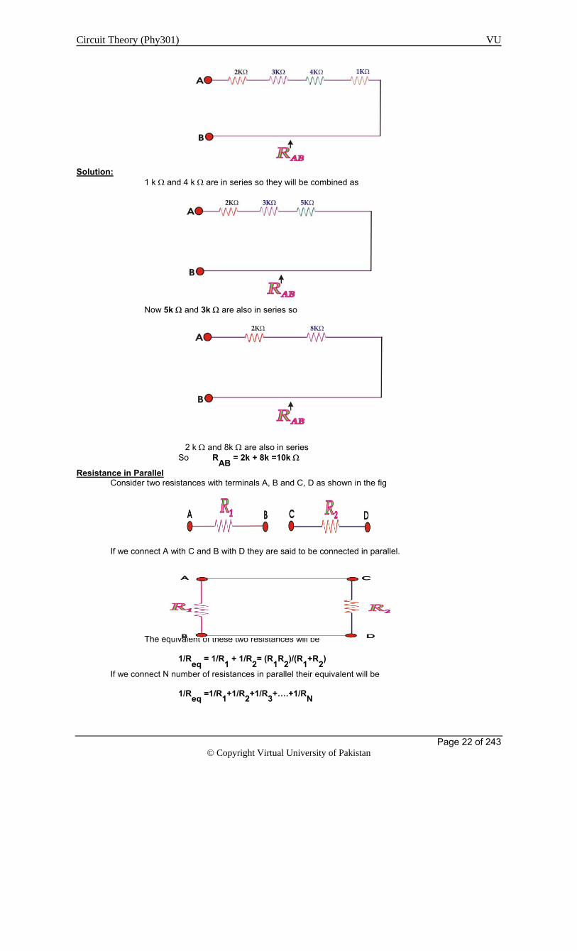
Solution: 1 k Ω and 4 k Ω are in series so they will be combined as
Now 5k Ω and 3k Ω are also in series so
2 k Ω and 8k Ω are also in series So RAB = 2k + 8k =10k Ω
Resistance in Parallel Consider two resistances with terminals A, B and C, D as shown in the fig
If we connect A with C and B with D they are said to be connected in parallel.
The equivalent of these two resistances will be 1/Req = 1/R1 + 1/R2= (R1R2)/(R1+R2)
If we connect N number of resistances in parallel their equivalent will be 1/Req =1/R1+1/R2+1/R3+….+1/RN

Circuit Theory (Phy301) VU
Page 23 of 243
© Copyright Virtual University of Pakistan
To illustrate this effect let us take some examples. Example 3 Simplify the given circuit.
1k is in parallel with 1k Ω so Req = (R1R2)/(R1+R2
= 1/2 =0.5 k Ω
Example 4 Simplify the given circuit.
4k Ω is parallel with 4k Ω so 4k||4k = (4 x 4)/(4 +4) =16/8 = 2k Ω
2k Ω is parallel with 2k Ω. So R
eq= (2 x2)/(2 +2) = 4/4
=1 K Ω

Circuit Theory (Phy301) VU
Page 24 of 243
© Copyright Virtual University of Pakistan
Example 5 Simplify the given circuit.
12k Ω is parallel with 4k Ω so 12k||4k = (12x4)/(4 +12) = 48/16 = 3k Ω
Now 2k Ω is in series with 3k Ω so R
AB= 2k +3k=5k Ω
Example 6 Simplify the given circuit.
4k Ω is in series with 8k Ω so the combined effect=12k Ω
12k Ω is in parallel with 12k Ω so 12k||12k=(12 x 12)/(12+12)

Circuit Theory (Phy301) VU
Page 25 of 243
© Copyright Virtual University of Pakistan
=144/24=6k Ω
4k Ω is in series with 6k Ω so their combined effect = 4k+6k =10k Ω
6k Ω is in parallel with 10k Ω so R
AB = (6 x 10)/(6+10)=3.75k Ω
Example 7 Simplify the given circuit.
3k Ω is in series with 6k Ω, therefore, their combined effect=3k +6k= 9k Ω
9k Ω is in parallel in 18k Ω so
9k||18k= (9 x 18)/(9+18) =162/27=6k Ω

Circuit Theory (Phy301) VU
Page 26 of 243
© Copyright Virtual University of Pakistan
6k Ω is in series with 10k Ω So their combined effect = 6k+10k =16k Ω
6k Ω is in series with 16k Ω so R
AB= 6+16 =22k Ω
Example 8 Simplify the given circuit. 1k Ω is in series with 2k Ω so Their combined effect= 1+2=3k Ω

Circuit Theory (Phy301) VU
Page 27 of 243
© Copyright Virtual University of Pakistan
3k Ω is in parallel with 6k Ω 3k||6k= (3 x 6)/(6+3) =18/9 =2k Ω
10k Ω is in series with 2k Ω, therefore, their combined effect =10k+2k=12k Ω
12k Ω is in parallel with 6k Ω, hence 12k||6k= (12 x 6)/(12+6)=4k Ω
2k Ω is in series with 4k Ω combined effect= 2+4=6k Ω

Circuit Theory (Phy301) VU
Page 28 of 243
© Copyright Virtual University of Pakistan
6k Ω is in parallel with 6k Ω, therefore, 6k||6k=(6 x 6)/(6+6)=36/12=3k Ω
3k Ω is in series with 9k Ω, therefore, combined effect=3k +9k=12k Ω
12k Ω is in parallel with 4k Ω so 12k||4k = (12 x 4)/(12+4)=48/16=3k Ω
2k Ω is in series with 3k Ω so R
AB=2k+3k=5k Ω
Circuit Theory (Phy301) VU
Page 29 of 243
© Copyright Virtual University of Pakistan
LECTURE 4 (Series parallel combination)
Inductance
Resistance offered by an inductor in an circuit is called inductance. The unit of inductance is Henry. It is denoted by L.
Inductance in Series
If we connect n inductances in series the combined effect of all these inductances is equal to the sum of individual inductance.
Leq= L1+L2+L3+…..+Ln Inductance in Parallel
we connect n inductances in parallel, the reciprocal of combined effect of all these inductances is equal to the sum of reciprocals of individual inductances.
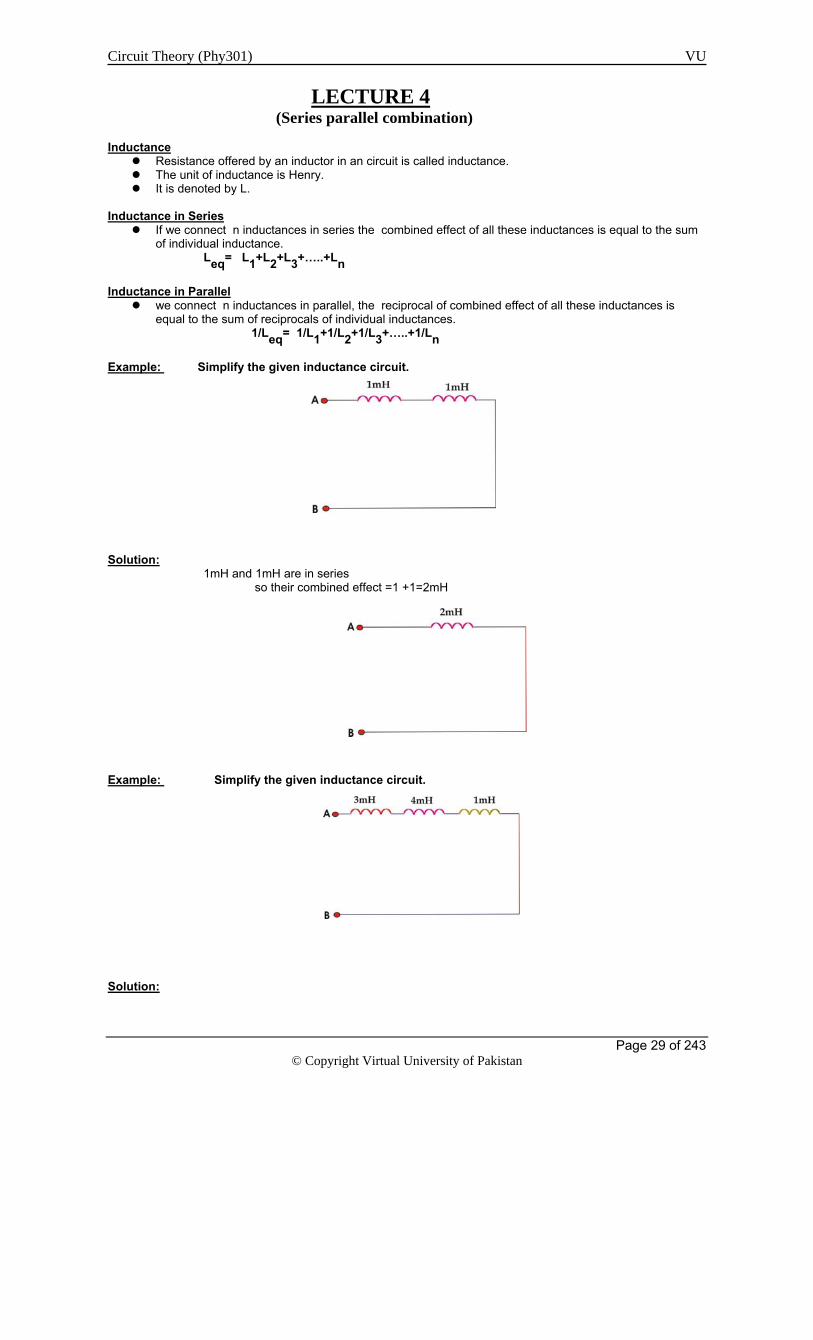
1/Leq= 1/L1+1/L2+1/L3+…..+1/Ln Example: Simplify the given inductance circuit.
Solution: 1mH and 1mH are in series so their combined effect =1 +1=2mH
Example: Simplify the given inductance circuit.
Solution:

Circuit Theory (Phy301) VU
Page 30 of 243
© Copyright Virtual University of Pakistan
1mH is in series with 4 mH and with 3mH, therefore, their effect=1 + 4+ 3=8mH
Example: Simplify the given inductance circuit.
Solution: 8mH is in parallel with 8mH so L
AB= (8 x 8)/(8+8
= 64/16 = 4mH
Example: Simplify the given inductance circuit.
Solution: 6mH is in parallel with 3mH so 6mH||3mH=(6 x3)/(6+3) =18/9 = 2mH

Circuit Theory (Phy301) VU
Page 31 of 243
© Copyright Virtual University of Pakistan
2mH is in parallel with 4mH, therefore,
2mH||4mH = (2 x 4)/(2+4) = 8/6=1.33mH
Example: Simplify the given inductance circuit.
Solution: 3mH is in parallel with 6mH so 3mH||6mH=(3 x6)/(3+6) = 18/9 = 2mH
2mH is in series with 2mH, therefore, The combined effect of these two = 2+2 = 4mH

Circuit Theory (Phy301) VU
Page 32 of 243
© Copyright Virtual University of Pakistan
4mH is in parallel with 4mH So 4mH||4mH = (4 x 4)/(4 +4) = 16/8 = 2 mH
1mH is in series with 2mH so L
AB=1+2=3mH
Capacitance:
Resistance offered by a capacitor in an circuit is called capacitance. The unit of capacitance is Farad. It is denoted by C.
Capacitance in parallel:
If we connect n capacitances in parallel the combined effect of all these capacitance is equal to the sum of individual capacitances.
Ceq= C1+C2+C3+…..+Cn Capacitance in Series:
If we connect n capacitances in series, the reciprocal of combined effect of all these capacitances is equal to the sum of reciprocals of individual capacitances.
1/Ceq= 1/C1+1/C2+1/C3+…..+1/Cn Example: Simplify the given circuit.
Solution: 2µF capacitor is in series with other 2µF capacitor their combined

Circuit Theory (Phy301) VU
Page 33 of 243
© Copyright Virtual University of Pakistan
effect will be= (2 x 2)/(2+2)=4/4=1µF
Example: Simplify the given circuit.
Solution: 12µF is in series with 4µF. So their combined effect will be = 48/16 =3µF
2µF is in series with 3µF so CAB =(2 x 3)/(2+3) =1.2µF
Example: Simplify the given circuit.
Solution: 4µF is in parallel with 12µF so 12||4=12+4=16µF
And 16µF is in series with 3µF so = (3x16)/(3+16) = 48/19 = 2.5µF
12µF is in parallel with 2.5µF so their combined effect will be

Circuit Theory (Phy301) VU
Page 34 of 243
© Copyright Virtual University of Pakistan
= 12 +2.5 =14.5µF
The capacitors are in series so CAB = (4 x14.5)/18.5 =3.13µF
OHM’S LAW:
If a voltage across a conductor is applied, the ‘current’ passing through the conductor is directly proportional to the ‘voltage provided temperature remains constant.’ i.e.
V α I V=IR
Where ‘R’ is the resistance of the conductor.
Resistance (‘R’) depends upon the material of the conductor. The Current “I=V/R”
If we keep the same resistance in a circuit but vary the voltage, the current will vary. For general case, for any values of ‘V’ & ‘R’ OHM’S Law is “I=V/R”. Where ‘I’ is the amount of current through resistance ‘R’, which is connected across a Potential
difference ‘V’. Volt (V) is the practical unit of potential difference & Ohm (Ω) for Resistance, therefore, Ampere=Volts/Ohms This Formula tells us, to calculate the Amperes of Current through ‘R’, simply divide the voltage across
‘R’ by the Ohms of Resistance. High Voltage but Low Current:
It is important to realize that with high voltage the Current can have a Low value when there is a very high Resistance in the circuit.
For example 1000 (1k) volts applied across 1000000 (1M) Ω results in a Current of only 0.001 (1m)A. The practical fact is that high voltage circuits usually do have a small value of current in electronic
equipment otherwise tremendous amount of power would be necessary for operation. Low Voltage but High Current:
At the opposite extreme a low value of voltage in a very low resistance circuit can cause a very high current to flow.
For example a 6 volt battery connected across a Resistance of .001Ω causes 600 A of Current to flow. I=V/R =6v/.01Ω =600 A Similarly more ‘R’ will result in less ‘I’. Example: A heater with a Resistance of 8Ω is connected across the 220 volt power line. How much is the current ‘I’ flowing through the heater coil? Solution: I=V/R =220/8 = 27.5 A

Circuit Theory (Phy301) VU
Page 35 of 243
© Copyright Virtual University of Pakistan
Example: A small light bulb with a resistance of 2400Ω is connected across the same 220 volt power line. How much is the current ‘I’ through the bulb filament? Solution: I=V/R =220/2400 =.09 A = 90m A The Voltage V=IR
It is the other Form of the same formula. Besides the numerical calculations possible with the ‘IR’ formula, it is useful to consider that the ‘IR’
product means voltage. Whenever, there is current through a resistance, it must have a potential difference across its two
terminals equal to the product ‘IR’. As we studied in the last lecture if there was no potential difference, no electrons could flow to produce
the current.
The Resistance R=V/I
As a third and final version of Ohm’s Law, three factors V, I, and R are related by the formula R=V/I. As we studied in the last lecture physically, a resistance can be considered as some material with
elements having an atomic structure that allows free electrons to drift through it. Electrically, a more practical & general way of considering Resistance is simply as a V/I ratio.
Example: A conductor allows 1 A of current with 10 volts applied at its ends. How much will be the Resistance of the conductor? Solution: R=V/I =10/1 =10 ohm The Linear Proportion Between V & I
The Ohm’s law formula V=IR states that V and I are directly proportional for any one value of R. This relation is true for constant values of R.
Volt-Ampere Characteristics The graph in figure is called the volt-ampere characteristic of R. It shows how much current the resistor
allows for different voltages.
Power Dissipation in Resistance
When current flows through a resistance, heat is produced due to friction between the moving free electrons and the atoms which obstruct the path of electron flow.
The heat is evidence that power is used in producing current. The electric energy converted to heat is considered to be dissipated or used up because the calories of
work can not be returned to the circuit as electric energy. Since power is dissipated in the resistance of a circuit, it is convenient to express the power in terms of
resistance R. The formula P=V x I can be arranged as follows. Substituting IR for V,
Circuit Theory (Phy301) VU
Page 36 of 243
© Copyright Virtual University of Pakistan
P =V x I =IR x I
=I2R
This is the common form of the formula because of heat produced in a resistance due to current R. For another form, substitute, V/R for I
P= V x I = V x V/R
= V2/R
In all the formulae, V is the voltage across R in ohms producing the current in amperes for power in Watts.
Circuit Theory (Phy301) VU
Page 37 of 243
© Copyright Virtual University of Pakistan
LECTURE 5
(AC, DC Current, voltages)
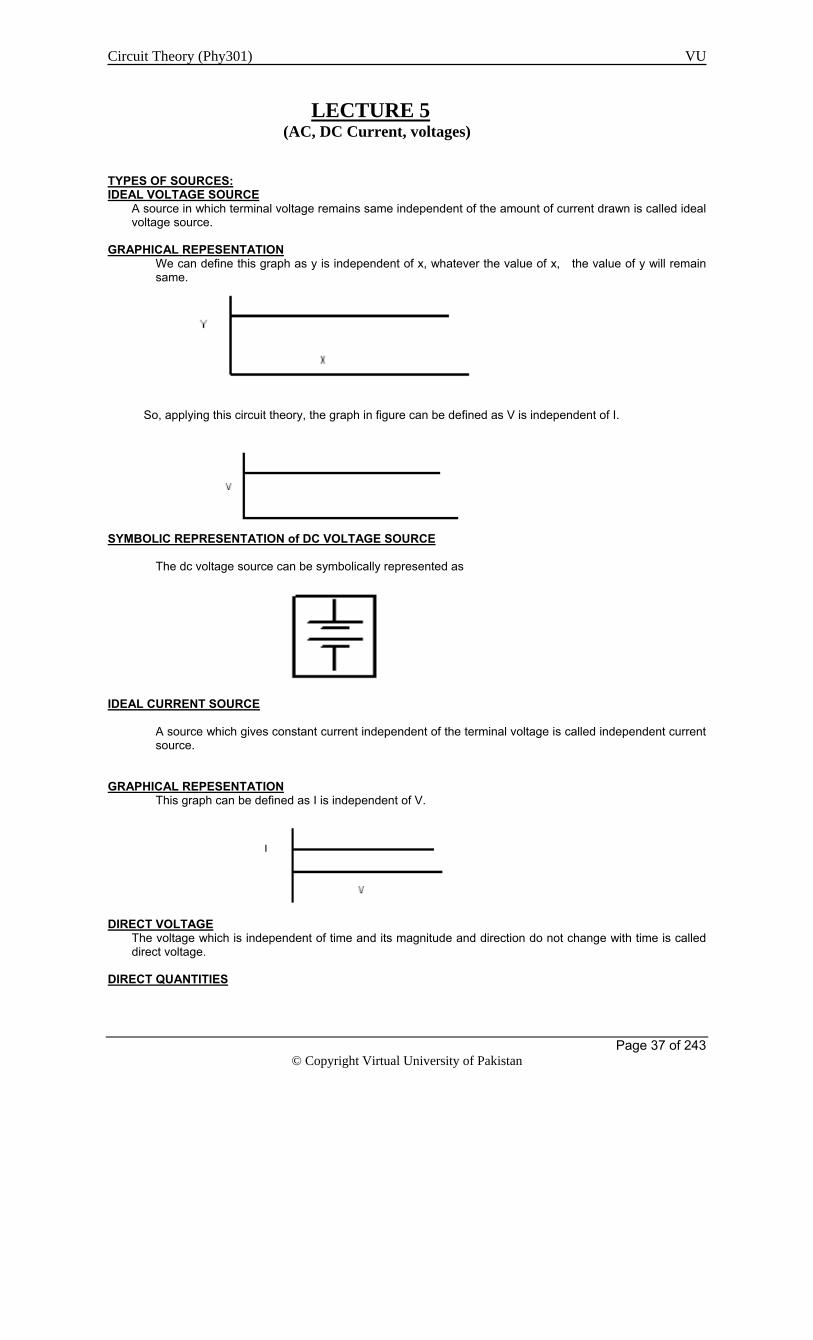
TYPES OF SOURCES: IDEAL VOLTAGE SOURCE
A source in which terminal voltage remains same independent of the amount of current drawn is called ideal voltage source.
GRAPHICAL REPESENTATION
We can define this graph as y is independent of x, whatever the value of x, the value of y will remain same.
So, applying this circuit theory, the graph in figure can be defined as V is independent of I.
SYMBOLIC REPRESENTATION of DC VOLTAGE SOURCE The dc voltage source can be symbolically represented as
IDEAL CURRENT SOURCE
A source which gives constant current independent of the terminal voltage is called independent current source.
GRAPHICAL REPESENTATION
This graph can be defined as I is independent of V.
DIRECT VOLTAGE
The voltage which is independent of time and its magnitude and direction do not change with time is called direct voltage.
DIRECT QUANTITIES

Circuit Theory (Phy301) VU
Page 38 of 243
© Copyright Virtual University of Pakistan
The quantities whose magnitude and direction do not change with time are called direct quantities for example may be V or I.
ALTERNATING QUANTITIES
The quantities whose magnitude and direction changes with respect to time are called alternating quantities. For example V or I.
DEPENDENT OR CONTROLLED SOURCES
VOLTAGE (1)Voltage controlled voltage source. (2)Current controlled voltage source. VOLTAGE CONTROLLED VOLTAGE SOURCE
The source whose magnitude is controlled by voltage is called voltage controlled voltage source. CURRENT CONTROLLED VOLTAGE SOURCE
Current controlled Voltage source can be defined as the source whose voltage is controlled by current is called current controlled voltage source.
VOLTAGE CONTROLLED VOLTAGE SOURCE
CURRENT CONTROLLED VOLTAGE SOURCE
VOLTAGE CONTROLLED CURRENT SOURCE
If magnitude of current is controlled by input voltage then the source is called voltage controlled current source.
CURRENT CONTROLLED CURRENT SOURCE
If magnitude of the current is controlled by input current the source is called current controlled current source.

Circuit Theory (Phy301) VU
Page 39 of 243
© Copyright Virtual University of Pakistan
Example
Solution: Figure shows a battery of 10 V has been applied across a resistor of 3k, so by Ohm’s law the current flowing through it, can be given as I =V/R =10/3k = 3.33 mA Example Calculate the Current I through the circuit.
Solution: 2kΩ and 3kΩ are in series so, the combined effect will be=2k + 3k = 5kΩ We want to calculate current through 5k Ω resistor.
The current flowing through 5kΩ resistor, by Ohm’s law I=V/R =10/5k =2 mA Example Calculate the Current I through the circuit.
Solution: The resistors of 25,10, and 5 ohm are in series, so their combined effect = 25+10+5 = 40Ω
The current flowing through 40 ohm resistor by Ohm’s law is I=V/R=40/40=1 A

Circuit Theory (Phy301) VU
Page 40 of 243
© Copyright Virtual University of Pakistan
Example: Find R1.
Solution: The current flowing through the resistor R1 is 5mA so by Ohm’s law the value of R1 is R=V/I R1 = 10V/5mA = 2kΩ Example: Find V.
Solution: The current flowing through 10k resistor is 3mA so the voltage, by Ohm’s law V =IR = 10k x 3m=30V Example: Find V.
Solution: 10k and 5k are in series so their combined effect will be = 5k+10k=15k The current flowing through the circuit is 2mA.
So by Ohm’s law, the voltage is V = IR = 2m x15k = 30V Example: Calculate the current through all the resistors in the circuit.

Circuit Theory (Phy301) VU
Page 41 of 243
© Copyright Virtual University of Pakistan
Solution: we need to simplify the circuit first. 3k||6k=(3 x6)/(3+6)=18/9=2k Ω
2k Ω is in series with 2k Ω so their combined effect =2k+2k=4k Ω
3k is in series with 1k so their combined effect= 3k+1k=4k
4k is in parallel with 4k, so 4k||4k=16/8=2k

Circuit Theory (Phy301) VU
Page 42 of 243
© Copyright Virtual University of Pakistan
The resistors 6kΩ, 2kΩ and 4kΩ are in series so they will be
combined as=6k+2k+4k=12k Ω.
So the current flowing through all resistors by Ohm’s law =12/12k
= 1k-1
A = 1mA Example: Find current through circuit.
Solution: 3k Ω is in parallel with 6k Ω, therefore, 3k||6k = (3 x 6)/(3 + 6) = 18/9 =2k Ω
4kΩ is series with 2kΩ so their combined effect = 2k + 4k = 6kΩ.
6k Ω is in parallel with 12k Ω so 6k||12k =(6 x 12)/(12+6) = 72/18 = 4k Ω

Circuit Theory (Phy301) VU
Page 43 of 243
© Copyright Virtual University of Pakistan
The resistors 2kΩ,4kΩ, 4kΩ are in series so the combined effect will be =2k+4k+4k =10kΩ So the current flowing through all the Resistors by Ohm’s law will be I=V/R =20/10k =2mA
VOLTAGE DIVIDERS AND CURRENT DIVIDERS:
Any series circuit is a voltage divider. The IR drops are proportional parts of the applied voltage. VOLTAGE DIVIDERS AND CURRENT DIVIDERS:
Special formulae can be used for voltage and current division as short cuts in calculations. The voltage division formula gives the series voltage even when the current is not known.
SERIES VOLTAGE DIVIDERS:
The current is same in all resistances in a series circuit. Also, the voltage drop is equal to the product IR. Therefore, IR voltages are proportional to series resistances.
A higher resistance has a greater IR voltage than a lower resistance in same series circuit; equal
resistances have the same amount of IR drop across each resistance. If R1 is double than R2 then V1 will be double than V2. The series string can be considered as a voltage divider. Each resistance provides an IR drop V equal to its proportional part of the applied voltage. Stated by
formula, V=R/RT x VT Example: Calculate the voltage drop across 4kΩ resistor
Solution: We want to calculate the voltage drop across 4kΩ resistor. So by voltage division rule V = (4/10) X 10 =4 volts
Now we want to calculate the voltage drop across 6k resistor so by formula V = (R/Rt) xVt =(6/10) x 10 = 6 volts

Circuit Theory (Phy301) VU
Page 44 of 243
© Copyright Virtual University of Pakistan
Example: Calculate the power dissipated in the Circuit. Solution: The circuit can be redrawn as:
12KΩ resistor is in parallel with 12K. So their parallel combination will be (12K x 12K)/(12K + 12K) = 6K
The circuit will become 6k is in series with 2k. So there combined effect will be = 6k +2k = 8k
8K||4K = 2.66K
2.66K||8K =2K

Circuit Theory (Phy301) VU
Page 45 of 243
© Copyright Virtual University of Pakistan
2K||4K =1.33K
So the current flowing through it I =12V/1.33K
= 9.022 mA So the power dissipation in the circuit
P = VI = 12 x 9.022 m A = 108.26 m

Circuit Theory (Phy301) VU
Page 46 of 243
© Copyright Virtual University of Pakistan
LECTURE 6 (Voltage divider, Current divider)
EXAMPLE: Find the voltage drop across each resistance.
Solution:
The voltage drop across 9k resistor V1 = (9/9+3) x 12 = 9/12 x 12 = 9 volts
The voltage drop across 3k resistor
V2 = (3/12) x12 = 3 volts. EXAMPLE: Find the voltage drop across each resistance.
Solution:
Three resistors are in series and we want to calculate the voltage drop across each resistor it will be calculated as The voltage drop across 50 k resistor
V = R/Rt xVt = 50k/100k x200 = 100V The voltage drop across 30k resistor V = 30/100 x 200 = 60 V The voltage across 20k resistor V = 20/100 x 200 = 40 volts EXAMPLE: Find the voltage across each resistance.
Solution:
As we studies in the last lecture same voltage appear across the parallel Resistances so the same 10v source voltage will appear across 10k resistor.

Circuit Theory (Phy301) VU
Page 47 of 243
© Copyright Virtual University of Pakistan
Now the voltage source is in parallel with the 1 k resistor so the voltage will be same.
Now 4k is in series with 4k so we can Apply voltage division rule
V= 4/8 x 10=5 volts TWO VOLTAGE DROPS IN SERIES
For this case, it is not necessary to calculate both voltages. After finding one we can subtract it from Vt to find the other.
As an example, assume Vt is 48V across two series resistances R1 and R2. if V1 is 18 volts then V2 must be 48 – 18= 3 volts 0vo
CURRENT DIVIDER WITH TWO PRALLEL RESISTANCES
It is often necessary to find individual branch currents in a circuit but without knowing the value of branch voltage.
This problem can be solved by using the fact that currents divide inversely as branch resistance. The formula is
I1 = IS X R2/(R1 + R2) EXAMPLE: Find the current through each resistance.
x IT
Solution: The current flowing through 4 ohm Resistor will be
I = 2/2+4 x 30 = 2/6 x 30
= 10A The current flowing through 2 ohm resistor
I = 4 /2+4 x 30 = 4/6 x30 = 20 A EXAMPLE: Find the current through each resistance.

Circuit Theory (Phy301) VU
Page 48 of 243
© Copyright Virtual University of Pakistan
Solution:
The same 30 A current is flowing through series combination 2k and 3k so they are leaving no effect on the value of current. Current divides at node A into two parts.
Now by current division rule the current flowing through 1k resistor I = 4/4+1 x30 = 4/5 x30
I = 24A EXAMPLE: Calculate the current through 4k Ω resistance.
Solution:
We want to calculate the current though 4k resistor. Current will divide in two parts at Node A. 2k Ω is in series with 2k Ω so the current flowing through 4k resistor Is
I = 4/4+4x 12 = 4/8 x12 I = 6 A EXAMPLE: Calculate the current through 8k Ω resistance.
Solution:
We want to calculate the current through 8k resistor. Now if we take the direction of current source downward the value of it will become -6A.Now the current flowing through 8k resistor can be calculated as
I = 4/12 x -6 = -2 A

Circuit Theory (Phy301) VU
Page 49 of 243
© Copyright Virtual University of Pakistan
EXAMPLE: Calculate the voltage across 3k Ω resistance.
Solution:
We want to calculate the voltage across 3kΩ resistor. At point A the current divides into two parts, one through 12kΩ resistor and other through series combination of 3kΩ and 1kΩ resistors.
So the current flowing through series combination of 1kΩ and 3kΩ can be calculated as I = 12/4+12 x 1
= 12/16 x1 I = 0.75 A
Same current is flowing through the series combination of two resistors so the voltage across 3kΩ resistor will be
V = IR = 0.75 x 3k V = 2250 volts Example: Find V.
Solution:
We want to calculate the voltage across entire circuit. 4kΩ resistor and 14kΩ resistor are in series so their combined effect =14+4=18kΩ.
18kΩ resistor and 9kΩ resistor are parallel 18k||9k = 18 x 9/27 =6kΩ

Circuit Theory (Phy301) VU
Page 50 of 243
© Copyright Virtual University of Pakistan
6k resistor is in parallel with 12kΩ resistor 6k||12k= 6 x 12/18= 4kΩ
2kΩ resistor is in series with 4kΩ resistor so the total resistance will be
= 2k+4k=6k Ω
So the voltage drop across the equivalent 6kΩ resistor V = IR
= 6k x 1 =6000volts.
Example: Find current through 6k ohm resistance.
Solution:
At point c the current should divide into two parts but due to short circuit between c and D whole current will come at point D.

Circuit Theory (Phy301) VU
Page 51 of 243
© Copyright Virtual University of Pakistan
Now by current division rule the required current will be I =(6k/12k) x 1
=0.5A Example Calculate the voltage across 4kΩ resistor.
Solution: We want to calculate the voltage across 4kΩ resistor if we take the direction of current source negative our circuit will become
The current is dividing between 3kΩ and series combination of 2kΩ and 4kΩ so by current division rule
I = (3k/(3k +6k))x (-2) = (3k/9k)x (-2)
=-0.66 A so the voltage across the 4kΩ resistor
V = IR = 0.66 x 4k
=2640 volts EXAMPLE: Calculate the value of current through 5k Ω resistance.
Solution:
We want to calculate the value of current though 5kΩ resistor. Look closely at the circuit. Resistor 5KΩ has zero resistance in parallel, so current arriving at node C, will take the zero resistance path and no current will pass through 5KΩ,

Circuit Theory (Phy301) VU
Page 52 of 243
© Copyright Virtual University of Pakistan
EXAMPLE: Calculate the voltage across 12k resistor.
Solution:
We want to calculate voltage across 12k resistor using voltage division rule.4k resistor is in parallel with 6V so same voltage will be dropped across it so we can omit this resistor from this circuit.
12 k ⎢⎢ 6k = 12k x 6k 12k + 6k
= 4k
Now applying Voltage division rule
4k x 6VV4k = 6k
= 4V Since 4k is the parallel combination of 6kand 12k. So the same voltage will be across 12k. So V0 = 4volts. EXAMPLE: Find power absorbed by each element.

Circuit Theory (Phy301) VU
Page 53 of 243
© Copyright Virtual University of Pakistan
Solution: Beginning from the left we find
P20 V = -(20)(4) = -80 V1.5 = 4(1.5) = 6V Therefore, p1.5 = (v1.5)2/1.5 = 24W V14 = 20 – V1.5 = 20 - 6 = 14V Therefore, p14 = 142 /14 = 14W i2 =V2/2 = V1.5/1.5–V14 /14 = 6/1.5–14/14 i2 =3A Therefore, V2 = 2(3 ) = 6V and p2 = 62/2 =18W V4 = V14 -V2 = 14 -6 V4 = 8V Therefore p4 = 82/4 = 16W i2.5 = V2.5/2.5 = V2/2 - V4/4 = 3 -2 i2.5 = 1A V2.5 = (2.5)(1) = 2.5 V and so p2.5 = (2.5 )2/2.5 p2.5 = 2.5W I2.5 = - Is Therefore Is = -1 A

Circuit Theory (Phy301) VU
Page 54 of 243
© Copyright Virtual University of Pakistan
LECTURE 7 (Kirchhoff's Laws Kirchhoff's Current Law (KCL)
Example:
(a) Calculate vy if iz = -3A. (b) What voltage would need to replace the 5v source to obtain vy = -6v if iz = 0.5A
Solution: (a) Vy = 1(3vx + iz) vx = 5V and given that iz = -3A, We find that vy = 3(5) - 3 = 12 V (b) Vy = 1(3Vx + iz) = -6 = 3vx + 0.5 Solving, we find that Vx = (-6 - 0.5) / 3 = -2.167V EXAMPLE: Calculate the source voltage Vs, while the voltage between node A and B is 4V.
Solution:
The voltage between node A and B is 4V the source voltage can be calculated as V = (R/ Rt) Vs
4 = (4/12) Vs Vs =(12 X 4)/4 = 112Volts EXAMPLE: Calculate the source current Is.
Solution:
We want to calculate the source current. The voltage across 3kΩ resistor is 12V. So the current (I) flowing through it, will be
I = V/R = 12/3k
= 4mA

Circuit Theory (Phy301) VU
Page 55 of 243
© Copyright Virtual University of Pakistan
The same current is following through the series combination of 3kΩ resistor and 9kΩ resistor. 3kΩ is in series with 9kΩ and 2kΩ is in series with 4kΩ, so
Now by current division rule the source current will be
I = (6k/(12k +6k)) Is Is = (18k/6k) 4mA
=12mA EXAMPLE: Calculate the source voltage Vs.
Solution:
We want to calculate the source voltage. The voltage across 2kΩ resistor is 4V, so the current flowing through it will be
I = V/R = (4/2k)
= 2mA
The same current is following through the series combination of 2kΩ and 4kΩ. So the voltage across 4kΩ resistor will be
V = IR = (2m) x (4k) = 8 Volts
So the total voltage across 2kΩ and 4kΩ resistor will be V = 4V +8V
=12V 4kΩ is in series with 2kΩ these may be combined as
=4k+2k=6kΩ
6kΩ is parallel with 6kΩ resistor so 6k||6k = (6x6)/(6+6) = 3kΩ

Circuit Theory (Phy301) VU
Page 56 of 243
© Copyright Virtual University of Pakistan
The voltage across 3kΩ resistor is 12V so the source voltage is
V = (3/(3+9)) Vs Vs =12 (12/3)
= 48V EXAMPLE: Calculate the voltage across 4kΩ resistor.
Solution:
We want to calculate the voltage across 4kΩ resistor. 12k||4k = (12 x4)/(12+4) = 3kΩ
9kΩ is in series with 3kΩ their combined effect will be = 9k +3k =12kΩ
12kΩ is parallel with 6kΩ resistor so
12k||6k = (12 x 6)/18 = 72/18 = 4kΩ
12kΩ is parallel with 4kΩ resistor so
12k||4k = (12 x4)/(12+4) = 48/16 = 3kΩ

Circuit Theory (Phy301) VU
Page 57 of 243
© Copyright Virtual University of Pakistan
So by voltage division rule, the voltage across the equivalent 3kΩ resistor is
V = (3/6)x12 = 6 V
So the voltage across 3kΩ resistor is
V = (3/12) x 6 =1.5 volts
The same voltage will be drop across 4kΩ resistor.
KIRCHHOF’S LAW KIRCHHOF’S CURRENT LAW
Sum of all the currents entering in the node is equal to sum of currents leaving the node. It can also be defined as Sum of entering currents + sum of leaving currents =0
ASSUMPTIONS
All the entering currents are taken as negative. All the leaving currents are taken as positive.
NODE It is the junction of two or more than two elements
OR It is simply a point of connection between circuit elements. BRANCH It is the distance or link between two nodes. LOOP
It is the closed path for the flow of current in which no node is encountered more than once. Let’s take some examples of node analysis or Kirchhof’s current law. Formula for Writing Equation
Number of equations in node analysis is one minus than the number of total nodes. Number of equations = N – 1 Where N is the number of nodes. Ground
This is a common or reference point among all the nodes without insertion of any component between.

Circuit Theory (Phy301) VU
Page 58 of 243
© Copyright Virtual University of Pakistan
Example: Find the value of I1 ,I2 ,I3 ,I4.
Solution:
Assuming the currents leaving the node are positive, the KCL equations for node 1 through 4 are
For node 1 -I1 +0.06 + 0.02 =0
- I1+0.08= 0
I1 = 0.08 A
For node 2 I1 - I4 + I6 =0
0.08 - I4 + I6=0
- I4 + I6 = -0.08 A
For node 3 -0.06+ I4 –I5 + 0.04 = 0
I4 – I5 = 0.02 A

Circuit Theory (Phy301) VU
Page 59 of 243
© Copyright Virtual University of Pakistan
For node 4 -0.02 +I5 -0.03 = 0
I5 = 0.05 A
Now putting the value of I5 in equation of node 3
I4 -0.05 = 0.02
I4 = 0.07 A
Putting the value of I6 in the equation for node 2
- 0.07 +I6 = -0.08
I6 = -0.01 A
EXAMPLE: Find Vx, Iin and Is.
Solution: (a) By KVL -2 + Vx + 8 = 0 So that VX = -6V (b) By KCL at the top right node Is + 4Vx = 4 - Vx / 4 So Is = 29.5A Iin = 1 + Is + Vx / 4 - 6 or Iin = 23A

Circuit Theory (Phy301) VU
Page 60 of 243
© Copyright Virtual University of Pakistan
LECTURE 8 (Application of Nodal Analysis)
Example: Write KCL equations for all nodes.
Solution:
The KCL equations for nodes 1 through 4 follow For node 1
I1 + I
2 – I
5 = 0
For node 2 -I
2 +I
3 -50I
2 = 0
For node 3 -I
1 + 50I
2 + I
4 = 0
For node 4 I
5 – I
3 – I
4 = 0
Example Write KCL equations for all nodes.
Solution: For node A 10mA is entering the node and the source current I
t is leaving and 60mA is also entering
so, For node A
It -60mA – 10mA= 0
For node B 60mA – 40mA – 20mA = 0

Circuit Theory (Phy301) VU
Page 61 of 243
© Copyright Virtual University of Pakistan
Example Write KCL equation for node A.
Solution:
By KCL the equation for node A -12mA + 4mA + I =0 Example Write KCL equation for node A and node B.
Solution:
The equation of currents at node A and B by KCL For node A
-I1+I
2+ 3mA = 0
For node B -12mA + 4mA +I
1=0
Example Write KCL equation for node A .
Writing equation for node A .
For node A -10 I
x+ I
x+44 mA – 12 mA = 0
Example Write KCL equation for node A .
Solution:
For node A equation will be by KCL Ix+ 10I
x – 44mA = 0

Circuit Theory (Phy301) VU
Page 62 of 243
© Copyright Virtual University of Pakistan
Example Calculate the values of I1 and I2.
Solution:
We want to calculate the values of I1 and I
2
For node A 4mA + 8mA- I
1 = 0
I1 = 12mA
Now for I2
For node B
-8mA + 2 mA + I2=0
I2
= 6mA
Example Calculate the values of I1 , I2 , and I3.
Solution:
We want to calculate the values of I1 , I
2 , and I
3, so we will use node analysis.
For node A
-I1
– I2
+8mA = 0
-I1
– I2
= -8mA
For node B I
2 + I
3 +4mA = 0
I2 + I
3 = - 4mA
For node C -I
3 + 2mA – 8mA = 0
I3 = - 6mA
Putting the value of I3 in equation of node B
I2
- 6mA = -4mA
I2
= 2mA
Putting the value of I2 in equation of node A
-I1 – 2mA = -8mA
I1
= 6mA

Circuit Theory (Phy301) VU
Page 63 of 243
© Copyright Virtual University of Pakistan
Example: Find the KCL equtations for node A,node B, node C and node D.
Solution: We want to write the equations for nodes A, B, C and D.
For node A -5mA + 8mA + 4mA =0 For node B I
1 – I
2 + 5mA =0
For node C -I
1 – 2mA + 3mA – 8mA =0
For node D -4mA – 3mA + I
3 = 00
Example Calculate the current Io.
Solution:
At node 1 (V1/12k) + ((V1 – V2)/10k) = 6mA 5V1 +6V1 – 6V2 = (60k)(6mA) 11V1– 6V2 = 360 At node 2
(V2/3k) +(V2/6k) + ((V2- V1)/10k) =0 10V2 +5V2+3V2-3V1=0
18V2 -3V1 =0 Equating equation of node1 and node 2
33V1 -18V2 =1080 -3V1 + 18V2 = 0 30V1 =1080
V1 = 36 volts 18V2 -3V1 =0 6V2 – V1=0 6V2 -36 =0
V2 = 36/6 V2 = 6volts I
o =V2/6k
= 6/6k = 1mA

Circuit Theory (Phy301) VU
Page 64 of 243
© Copyright Virtual University of Pakistan
Example: Use nodal analysis to determine the value of V2 that will result in V1 = 0
Solution: If V1 = 0, the dependent source is a short circuit and we may redraw the circuit as :
At NODE 1 : 4 - 6 = V1/40 + (V1 - 96)/20 + (V1 - V2)/10 Since V1 = 0, this simplifies to -2 = -96/20 - V2/10 So that V2 = -28V
Example Use nodal analysis to find V1 and V2, compute the power absorbed by 6Ω resistance. Solution: Designate the node between the 3 Ω and 6 Ω resistors as node X, and the right hand node of the 6Ω resistor node Y. The bottom node is chosen as the reference node. (a) Writing the two nodal equation, then NODE X : -10 = (Vx - 240)/3 + (Vx - Vy)/6 [1] NODE Y : 0 = (Vy - Vx)/6 + Vy/30 + (Vy - 60)/12 [2] Simplifying, -180 + 1440 = 9Vx – 3Vy [1] 10800 = -360Vx + 612 Vy [2] Solving Vx = 181.5V and V y = 124.4V Thus, V1 = 240 - Vx = 58.50V and V2 = Vy - 60 = 64.40V (b) The power absorbed by the 6Ω resistor is (Vx - Vy)2 / 6 = 543.4 W

Circuit Theory (Phy301) VU
Page 65 of 243
© Copyright Virtual University of Pakistan
LECTURE 9 (Application of Nodal Analysis)
Example Find current flowing through 6k ohm resistor.
Solution:
At node 1 ((V1- V2)/6k) + (V1/3k) =2mA V1 – V2 +2V1 =6k x 2mA -V2 + 3V1 =12 9V1 -3V2 = 36 …………………..(A)
At node 2 V2/12k +4mA +(V2-V1)/6k =0 V2+48+2V2-2V1=0 3V2 – 2V1 = -48 ………………(B)
Adding equation (A) & (B)
3V2 – 2V1 = -48 -3V2+ 9V1 = 36 V1= -12/7
Now putting the value of V1 in (A) V2= 3V1-12 = 3 x (-12/7) -12 = (-36/7) -12 = (-36-84)/7 V2 = -120/7
V0 =V2 – V1 = (-120/7) + 12/7 = -108/7
I0 = -108/7 x (1/6k) =-108/42 = 2.57 mA

Circuit Theory (Phy301) VU
Page 66 of 243
© Copyright Virtual University of Pakistan
Example Find voltage across 2k ohm resistor.
Solution:
Combine 2k and 2k and then At node (1) V1/3k +4mA +2mA + (V1-V2) /6k =0 2V1 +24 +12 +V1 – V2 =0
3V1 –V2 = -36 At node (2) V2/4k + V2/12k - 2mA +(V2 –V1)/6k = 0 3V2 +V2– 24 + 2V2 – 2V1 = 0 6V2 – 2V1 = 24
9V2 – 3V1 =36
-V2 + 3V1 =-36
8V2 =0 V2 =0
you can see from the circuit on the right side two resistance are in series i:e 2k and 2k ohm so we will apply voltage divider rule here
V0
= 2/4 x V2 = 2/4 x 0 = 0
Example : Find current flowing through 4k ohm resistor.
Solution: At node 1 (V1-12)/12k + V1/6k + (V1+6) /4k = 0 V1 – 12 + 3V1 + 3(6) +2V1= 0 6V1 = -6 V1= -6/6 = -1 volts
Io = (V1 –(–6))/4k
Here negative sign with -6 is due to the negative reference of the battery ,so

Circuit Theory (Phy301) VU
Page 67 of 243
© Copyright Virtual University of Pakistan
Io= (-1+6)/4k
= 5/4 Io=1.2mA
Example : Find voltage across1k ohm resistor.
Solution:
As we see in the circuit 2k and 1k ohm resistors are in series and the same current will pass through them so we will combine them and they will become 3k ohm So,
At node 1 (V1 + 6)/6k + (V1+3)/2k +V1/3k = 0 6 + V1+9 +2V1+3V1 = 0 6V1+15 = 0 V1 = - 15/6 volts
By Voltage divider rule at V0 V0 = 1/3 x -15/6
= -5/6 volts Example : Find the voltage across a 12K ohm resistance. When we don’t know the value of the current in the circuit.
Solution: In this circuit we have three nodes one is reference node while the other node is between the 6v battery and the 12K resistance here we will neglect this node and calculate the voltage at point A so the node equation for the node V1 is
At node (1) (V1 – 12)/6k + (V1 -6)/12k +V1/6k = 0 5V1 = 30 V1 = 6volts
As we know that we want to calculate the voltage across 12K resistor and it is between 6V battery and V1 So, V0 = V1 - Vs In the above equation Vs =6V
V0 = V1 -6 = 0 volts

Circuit Theory (Phy301) VU
Page 68 of 243
© Copyright Virtual University of Pakistan
Example : Find the current Io through the 12K ohm resistor.
Solution:
At node 1 (V1+6)/12 + V1/12 + (V1 – V2)/12 = 0 V1 + 6 +V1 +V1 –V2 = 0 3V1 –V2 = -6 ---------------- (A) Multiplying both sides by 2 6V1 – 2V2 = -12 ----------------- (A1) At node 2
(V2 – V1)/12 + V2/12 = 2mA V2 –V1 +V2 = 24 2V2 –V1 =24 --------------------- (B) adding equation A1 & B we have
2V2 - V1 = 24 - 2V2 + 6V1= -12 5V1 = 12 V1=12/5 Put the value of V1 in A we have
V2 =3V1 +6 =3 x 12/5 + 6 =(36 + 30)/5 V2=66/5 Now we know the voltage at both nodes so now we will calculate the value of current through 12K resistance. So for output current Io I
o = (V1 – V2)/12
= (12/5 – 66/5)/12 = -54/5 x 1/12 = - 54/60 =-0.9mA

Circuit Theory (Phy301) VU
Page 69 of 243
© Copyright Virtual University of Pakistan
Example: Use nodal analysis to find VP.
Solution: The bottom node has the largest number of branch connections, so we choose that our reference node. This also makes VP easier to find, as it will be a nodal voltage. Working from left to right, we name our nodes 1, P, 2, 3. At node 1 10 = V1/20 + (V1 - Vp)/40 [1] At node p 0 = (Vp - V1)/40 + Vp/100 + (Vp - V2)/50 [2] At node 2 -2.5 + 2 = (V2 - Vp)/50 + (V2 - V3)/10 [3] At node 3 5 - 2 = V3/200 + (V3 - V2)/10 [4] Simplifying 60 V1 - 20 Vp = 8000 [1] -50 V1 + 110 Vp - 40 V2 = 0 [2] - Vp + 6 V2 - 5 V3 = -25 [3] - 200 V2 + 210 V3 = 6000 [4] Solving, Vp = 171.6V

Circuit Theory (Phy301) VU
Page 70 of 243
© Copyright Virtual University of Pakistan
Example: Use nodal analysis to find the value of K that will cause VY to be zero. Solution: At node x : VX/4 + (VX - VY)/2 + (VX - 6)/1 = 0 [1] At node y : (VY - K VX)/3 + (VY - VX)/2 = 2 [2] Our additional constraints is that VY = 0, so we may simplify Equations [1] and [2]. 14 VX = 48 [1] -2K VX - 3 VX = 12 [2] Since Eq. [1] yields VX = 48/14 = 3.429 V From equation 2 we have K = (12 + 3 VX)/(-2 VX) After putting the values of VX K = -3.250 Example: Use nodal Analysis to find I5 Solution: We choose the bottom node as ground to make calculation of i5 easier. The left-most node is named "1", the top node is named "2", the central node is named "3", and the node between the 4W and 6W resistors is named "4". NODE 1 :
-3 = v1/2 + (v1 - v2)/1 [1] NODE 2 :
2 = (v2 - v1)/1 + (v2 - v3)/3 + (v2 - v4)/4 [2] NODE 3 :
3 = v3/5 + (v3 - v4)/7 + (v3 - v2)/3 [3] NODE 4 :
0 = v4/6 + (v4 - v3)/7 + (v4 - v2)/4 [4] Rearranging and grouping terms,

Circuit Theory (Phy301) VU
Page 71 of 243
© Copyright Virtual University of Pakistan
3v1 - 2v2 = -6 [1] - 12v1 + 19v2 - 4v3 - 3v4 = 24 [2] - 35v2 + 71v3 - 15v4 = 315 [3] - 42v2 - 24v3 + 94v4 = 0 [4] Solving, we find that v3 = 6.76V and so i5 = v3/5 = 1.352 A
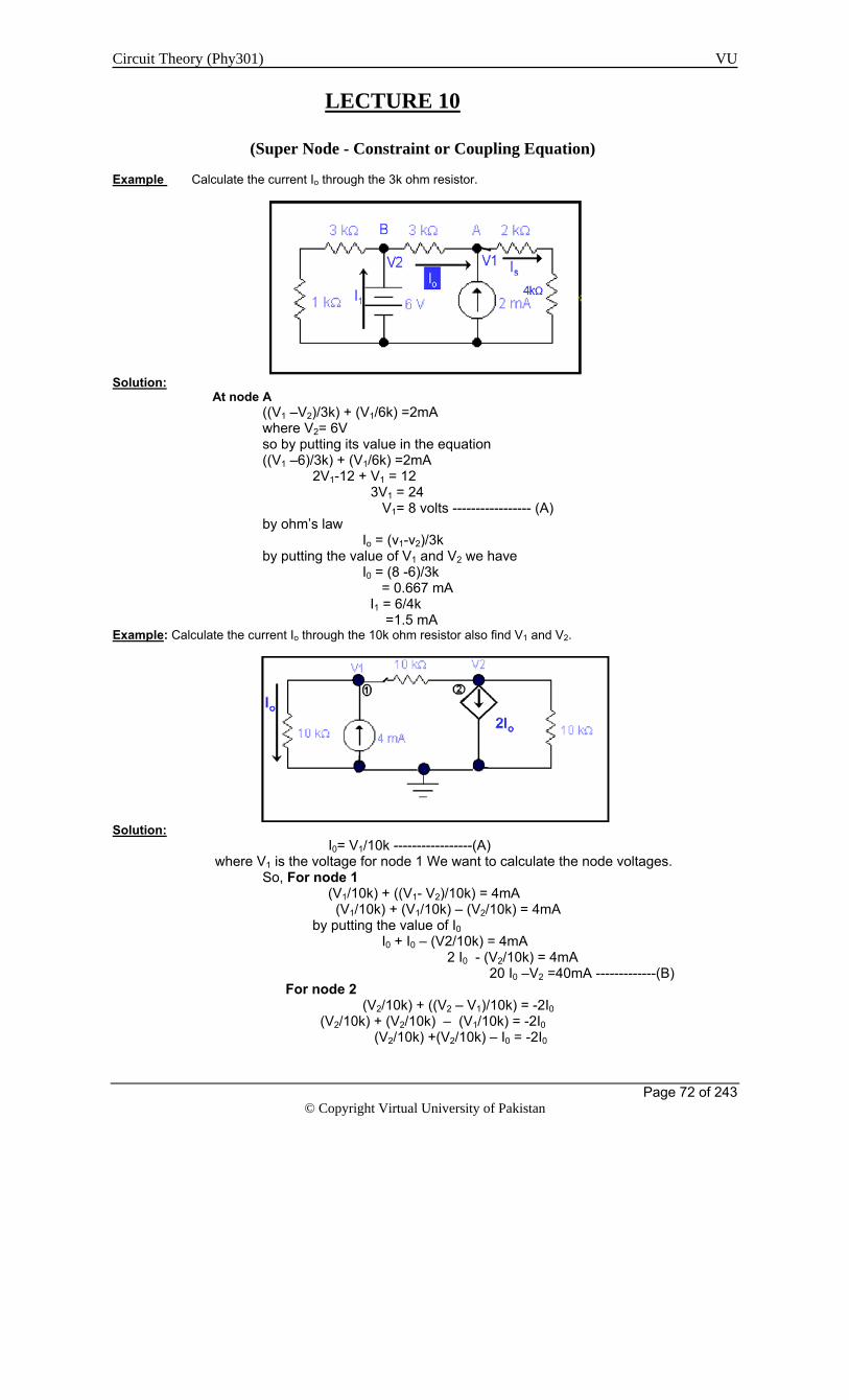
Circuit Theory (Phy301) VU
Page 72 of 243
© Copyright Virtual University of Pakistan
LECTURE 10
(Super Node - Constraint or Coupling Equation) Example Calculate the current Io through the 3k ohm resistor.
Solution:
At node A ((V1 –V2)/3k) + (V1/6k) =2mA where V2= 6V so by putting its value in the equation ((V1 –6)/3k) + (V1/6k) =2mA 2V1-12 + V1 = 12 3V1 = 24 V1= 8 volts ----------------- (A) by ohm’s law Io = (v1-v2)/3k by putting the value of V1 and V2 we have
I0 = (8 -6)/3k = 0.667 mA I1 = 6/4k =1.5 mA
Example: Calculate the current Io through the 10k ohm resistor also find V1 and V2.
Solution:
I0= V1/10k -----------------(A) where V1 is the voltage for node 1 We want to calculate the node voltages.
So, For node 1 (V1/10k) + ((V1- V2)/10k) = 4mA
(V1/10k) + (V1/10k) – (V2/10k) = 4mA by putting the value of I0 I0 + I0 – (V2/10k) = 4mA 2 I0 - (V2/10k) = 4mA 20 I0 –V2 =40mA -------------(B) For node 2 (V2/10k) + ((V2 – V1)/10k) = -2I0 (V2/10k) + (V2/10k) – (V1/10k) = -2I0 (V2/10k) +(V2/10k) – I0 = -2I0

Circuit Theory (Phy301) VU
Page 73 of 243
© Copyright Virtual University of Pakistan
2V2 + 10I0 = 0 ----------------(C) Equating equations of node 1 and 2
40 I0 - 2V2 = 80mA
10 I0 + 2V2 = 0
50 I0 = 80mA
Hence I0 = 8/5 mA
So, put the value of I0 in equation (A) I0
= (V1/10k) 8/5 mA = (V1/10k) V1 = 16 volts by putting the value of I0 from (A) into (C) we have 2V2 + V1 =0 2V2 =-V1 V2 = -16/2 = -8volts SUPER NODE:
A node which emerges as a result of combination of two ordinary nodes around a voltage source. CONSTRAINT OR COUPLING EQUATION:
This is an equation which describes a super node mathematically, instead of writing equations individual ordinary nodes of the super node.
Example Calculate the power supplied by current source.
Solution:
Power = 1A(V1) Applying KCL to node 1 (V1/10) - I
x = 1
Apply KCL to node 2 0 = Ix+(V2/5)+((V2-2)/ 7) Now, 3 unknown quantities can not be calculated from 2 equations, so try super node technique,
Equation for super node 1 = (V1/10) + (V2/5) + ((V2-2)/7) Simplifying it, we can write
35 V1+120 V2 = 450

Circuit Theory (Phy301) VU
Page 74 of 243
© Copyright Virtual University of Pakistan
Also the constraint or coupling equation is V1 - V2 = 6 Solving the two equation simultaneously,
35V1+120V2=450 -------- (A) V2 = V1 – 6 put the value of V2 in A we have 35V1 + 120(V1 – 6) = 450 35V1 + 120V1 –720 = 450 155 V1= 1170 V1= 7.55V
Therefore,
V1= 7.55 V & V2 = 1.55 V
Hence, power P = 1(A) (V1) = 7.55 W
Example: Calculate I1 from the given circuit.
Solution: We can redraw the circuit as
Constraint equation for super node V1 – V2 = 3
KCL equation for super node
(V1/3k) + (V2 /6k) = 2 x 10⁻³
2V1 + V2 =12
Now from constraint equation V2 = V1- 3
Putting this value in the KCL equation of super node 2V1 + V1 – 3 = 12 3V1 = 15 V1 = 5 volts Now I1 = 1 3k
=5/3k =1.6 mA

Circuit Theory (Phy301) VU
Page 75 of 243
© Copyright Virtual University of Pakistan
Example: Find I1 from the circuit.
Solution: We will redraw this circuit as
Constraint equation for the super node
V2 – V1 = 6V KCL equation for the super node ((V1 – 3)/6k) + (V1/12k) + ((V2 +3)/12k)+(V2/12k) = 0
2V1 -6 + V1 +V2 + 3 + 2V2 = 0 3V1 + 3V2 = 3 V2 + V1 =1
Adding constraint equation and KCL equation V2 – V1=6 V2 + V1=1
2V2 = 7 or V2 = 3.5V I
1 = 3.5/6k
=35/60k =7/12 mA Example: Calculate the value I1.
Solution:
We want to calculate the value of current I1
For node 1 (V1/12k) +(V1/4k) +(V1/6k) – (6/6k) = 2 mA ((1/12k) +(1/4k) +(1/6k))V1 –(6/6k) = 2 mA
(V1/2k) – (1/1k) = 2 x 10⁻³
V1 – 2 = 4
V1 = 6V Now
I1 =V1/4k
= 6/4k = 1.5 m

Circuit Theory (Phy301) VU
Page 76 of 243
© Copyright Virtual University of Pakistan
LECTURE 11
(Examples of Nodal Analysis - Super Node technique)
Example: Find the out put voltage V0.
Solution: we can redraw this circuit as
Here V1 = 6 and the constraint equation is V1 – V3 = 3V 6 - V3 = 3V V3 = 6 - 3 volts V3 = 3 volts Also, V3=V0 = 3 volts So V0 = 3 Volts

Circuit Theory (Phy301) VU
Page 77 of 243
© Copyright Virtual University of Pakistan
Example: Calculate V0 and I0.
Solution: Node 2 and 3 constitute a super node Constraint equation will be V2 – V3 = 6 ----------------------(A) KCL equation at super node is ((V2-12)/6k) + (V2/3k) + (V3 /6k) + ((V3 -12)/12k)=0 (V2/6k) + (V2/3k) + (V3 /6k) + (V3 /12k) – (12/12k) – (12/6k) = 0 (V2/2k) + (V3 /4k) – (12/4k) =0 2V2 +V3 – 12 = 0 2V2 + V3 = 12 ……(B) Now from constraint equation (A), value of V3 is V3 =V2 -6 put this in equation (B) Also, the super node equation becomes 2V2 +V2 -6 =12 3V2 = 18 V2= 6 Volts Putting this value in super node equation V3 =0 Therefore, Vo =0 Volt I0 = V2/3k =6/3k =2mA

Circuit Theory (Phy301) VU
Page 78 of 243
© Copyright Virtual University of Pakistan
Example: Calculate the value of V0.
Solution: The circuit can be redrawn as
Node 2 and 3 constitute a super node, having constraint equation V3 – V2 = 6volts KCL equation at super node ((V2 – 6)/6k) + (V2/12k)+ ((V3-6)/4k)+ (V3/12k) + (V3/6k) = 0 (V2/6k) + (V2/12k) + (V3/6k) + (V3/12k)+ (V3/4k) – (6/4k) – (6/6k) =0 (V2/4k) + (V3/2k) – (30/12k) =0 3V2 +6V3 – 30 =0 V2 + 2V3 =10 -----(A) From the constraint equation of super node V2 =V3 -6 KCL equation (A) of super node will become 3V3 – 6 =10 V3 = 16/3 volts V2 = (16/3) – 6 = – 2/3 V Now by voltage division rule V0 = (4k x V3)/(2k + 4k) = 64/18 = 3.55 Volts

Circuit Theory (Phy301) VU
Page 79 of 243
© Copyright Virtual University of Pakistan
Example: In the given circuit, find Vo.
Solution: Applying KCL at node 1 (V1/10k) = 3mA – 2 Ix Now Ix = (V1/10k) Putting this value in the equation of node 1 V1/10k = Ix=3mA -2Ix Ix = 1mA Now KCL at node 2 (V2/10k) = 2Ix (V2/10k) = 2 (1mA) V2 = 20 Volts = Vo Example: Find Io in the given circuit.
Solution: KCL equation for node 1 ((V1 – 6)/4k) + (V1/10k) + ((V1 – 12)/2k) = 0 5V1 – 30 + 2V1 +10V1 – 120 = 0 17 V1 = 150 V1 = 8.82 Volts I0 = (V1- 12 )/2k = (8.82 – 12)/2k I0 = - 1.58 mA So the current value is in negative sign, so we conclude that as it is given in the circuit the direction of Io is opposite.

Circuit Theory (Phy301) VU
Page 80 of 243
© Copyright Virtual University of Pakistan
LLEECCTTUURREE 1122 (Kirchhoff's Voltage Law (KVL) - Loop - Examples)
KIRCHHOFF’S VOLTAGE LAW: This law states that the algebraic sum of the voltages around any loop is zero. OR Sum of voltages rises and voltage drops around any closed path or loop is equal to zero. LOOP:
It is the closed path for the flow of current in which no node is encountered more than one Loop can be considered as closed path in which work done in moving a unit charge is equal to zero.
ASSUMPTIONS:
Any increase in energy level is taken as positive and any decrease in energy level is taken as negative. Current leaving the source is taken as positive and current entering the voltage source is taken as negative.
NO. OF EQUATIONS:
No. of equations to be written are equal to the no. of loops or closed paths. Example:
We want to calculate the value of VR3 where values of VR1 and VR2 are known by using KVL. Solution: Now we will take increase in energy level positive and decrease in energy level negative. By using this assumption and KVL the equation of this loop will be +VR1 - 5 + VR2 – 15 +VR3 – 30 =0 which can be written as VR1+ VR2 +VR3 = 5 +15 +30 = 50 Now suppose that VR1 and VR2 are known to be 18V and 12V respectively then VR3=20V

Circuit Theory (Phy301) VU
Page 81 of 243
© Copyright Virtual University of Pakistan
Example:
Solution: Note that this network has three closed paths the left loop, the right loop and outer loop. Applying KVL to left loop VR1+ VR4– 16 – 24 = 0 KVL equation for right loop starting at point B. VR2 + VR3 +8 +16 –VR4=0 The equation for outer loop starting at point A VR1 +VR2 +VR3 + 8 – 24 =0 Note that if we add first two equations, we obtain the third equation. So these three equations are not linearly independent. We will discuss this issue in next lectures that we will use only linearly independent equations to solve for all voltages.

Circuit Theory (Phy301) VU
Page 82 of 243
© Copyright Virtual University of Pakistan
LECTURE 13 (Applications of Loop Analysis)
Example: Calculate the voltages VAE and VEC.
Solution: We will draw some imaginary arrows across point A E and C. The circuit can be redrawn as
Since points A and E as well as E and C are not physically close, we use the arrow notation. Our approach to determining the unknown voltage is to apply KVL with the unknown voltage in the closed path, therefore to VAE we will use the path AEFA or ABCDEA.
The equation for two paths in which VAE is the only known are
For path AEFA VAE +10 – 24 = 0 ------------- (A) VAE = 14 volt For path ABCDEA 16 – 12 +4 +6 – VAE =0 ------------- (B) VAE = 14 volt Solving both loops i.e. AEFA and ABCDEA we will get VAE = 14 volt. We can calculate VEC using paths CDEC or CEFABC. The value of VAE is also known so we can also use path CEABC. KVL for each of the paths is For the loop or path CDEC 4 + 6 + VEC= 0 ------------- (1) VEC = -10 volts For the loop or path CEABC
-VEC +VEA +16 – 12 = 0 ------------ (A) in above equation (A) VEA= -VAE +VEC - VAE +16 – 12 = 0 ------------ (2) For the loop or path CEFABC -VEC +10 – 24 + 16 – 12 =0 ------------ (3) Solving each of three equations we have VEC = -10 volts

Circuit Theory (Phy301) VU
Page 83 of 243
© Copyright Virtual University of Pakistan
Example: Write KVL equations for the given circuit.
Solution: We have two loops in this circuit one is on the left hand side i.e. ABCA and other is on the right hand side i.e. BDCB. KVL equation for left hand loop ABCA VR1 +VR2 – Vs =0 KVL equation for right hand loop BDCB 20VR1 + VR3 – VR2= 0 Example: Calculate the voltage Vbd
Solution: We want to calculate the voltage Vbd. As we can see there is no closed path between b and d, so the circuit can be redrawn as
We can consider two closed paths abda and bcdb . The KVL equation for these two paths will be written as The KVL equation for the path abda 2 + Vbd -9 = 0 Vbd = 7 volts KVL equation for the bcdb 4 + 3 - Vbd = 0 Vbd = 7 volts

Circuit Theory (Phy301) VU
Page 84 of 243
© Copyright Virtual University of Pakistan
LECTURE 14
(Applications of Loop Analysis) EExxaammppllee:: FFiinndd tthhee ppoowweerr ddiissssiippaatteedd bbyy 33ΩΩ rreessiissttaannccee..
Solution: We can write I3=I1-I2, I1 and I2 are opposite to each other so they cancel each other up to some extent to give I3.It is given in the circuit that direction of I1 is in clock wise direction while I2 is also in clockwise direction. We suppose that voltage Vx for mesh 1 and Vy for mesh 2 across the 3 ohm resistance.
For mesh 1 -(-2)+ V5 +Vx=0 Also from Ohm’s law V5 = 5 I1 and Vx=3 ( I1 - I2 )
... 2+5I1+3(I1-I2) = 0
Or 8I1-3I2 = - 2 ------------- (A) For mesh 2 3( I2 – I1 ) + 2 I2 + 3 = 0 Or – 3I1 + 5I2 = –3 --------------- (B) Solving two mesh equations (A) and (B), we get I1 = – 612.9 mA I2 = – 967.7 mA
... I3=354.8 mA

Circuit Theory (Phy301) VU
Page 85 of 243
© Copyright Virtual University of Pakistan
Hence Power = 3 (354.8)2 =377.7 mW It does not matter whether we write I1-I2 or I2-I1 due to square term. Now using nodal analysis
0 = (V-(-2)/5) + (V/3) + (V-3)/2) V = 1.065V
... Power3Ω = | (V2/R)=378.1 mW
Example:
Calculate the voltage Vcf in the network.
Solution:
We want to calculate the voltage Vcf in the network. The network can be redrawn as
We can consider two paths for finding voltage Vcf that are abcfa and cdefc.
KVL equation for the path abcfa

Circuit Theory (Phy301) VU
Page 86 of 243
© Copyright Virtual University of Pakistan
-4 +9 + Vcf
-6 =0
Vcf = 1 volts ----------------- (A)
KVL equation cdefc will be -5 - 6 – 12 + Vfc
=0
Vfc= -1Volts ---------------(B)
In the above equation we have Vfc instead of Vcf . But we want to calculate Vcf.
Where Vcf = -Vfc so from equation B we have
Vcf = 1Volts
Example Calculate the voltage Vad Vce in the network.
Solution:
We want to calculate and Vad
V ce
. As there is no physical closed path in between these points the
circuit can be redrawn as
For Vad
There are two paths in which Vad
is the only unknown quantity they are adea and adcba.
For path adea the KVL equation will be V
ad -1V – 4Vx =0
where Vx=2V V
ad – 1 – 8=0
Vad = 9 volts
For the path adcba V
ad -12 +2 + 1 = 0
Vad = 9 volts
Note: Calculate V ce yourself.
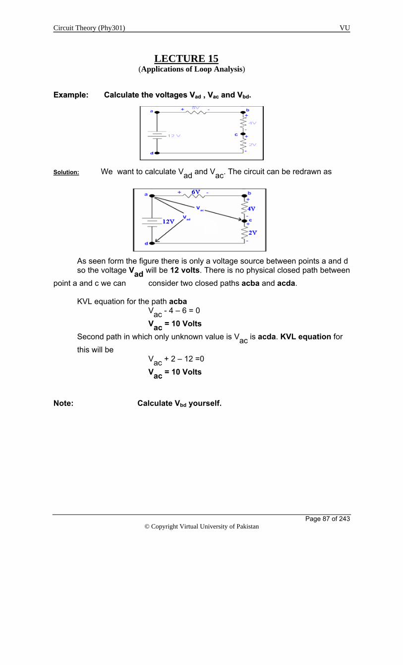
Circuit Theory (Phy301) VU
Page 87 of 243
© Copyright Virtual University of Pakistan
LECTURE 15
(Applications of Loop Analysis)
EExxaammppllee:: CCaallccuullaattee tthhee vvoollttaaggeess VVaadd ,, VVaacc aanndd VVbbdd..
Solution: We want to calculate Vad and Vac. The circuit can be redrawn as
As seen form the figure there is only a voltage source between points a and d so the voltage Vad will be 12 volts. There is no physical closed path between point a and c we can consider two closed paths acba and acda. KVL equation for the path acba Vac - 4 – 6 = 0 Vac = 10 Volts Second path in which only unknown value is Vac is acda. KVL equation for this will be Vac + 2 – 12 =0 Vac = 10 Volts Note: Calculate Vbd yourself.

Circuit Theory (Phy301) VU
Page 88 of 243
© Copyright Virtual University of Pakistan
Example: Calculate the voltages Vac and Vdb.
Solution: We want to calculate Vac and Vdb. The circuit can be redrawn as
To calculate Vac, the two paths will be acda and acba. KVL equation for the path acda Vac + 8 – 12 =0 Vac = 4 volts KVL equation for the path acba will be Vac + 6 – 10 = 0 Vac = 4 volts Two paths for Vbd will be bdcb and bdab. KVL equation for bdcb Vbd -8 +6 = 0 Vbd = 2 volts Vdb = - 2 volts KVL equation for the path bdab Vbd – 12 +10 =0 Vbd = 2 volts Vdb = - 2 volts

Circuit Theory (Phy301) VU
Page 89 of 243
© Copyright Virtual University of Pakistan
Example: Calculate the voltage V0 .
Solution: We want to calculate V0 . Here I2 = 2 mA KVL for mesh 1 3kI1 + 6k (I1 – I2) -12 = 0 9kI1 – 6kI2 = 12 9kI1 – 12 =12 I1 = 8/3 mA Voltage across 6k resistor V = 6k( I1 – I2) = 6k(8/3 – 2 = 4 volts As current through 2k resistor is I2 = 2mA Voltage across 2k = 2k x 2mA = 4 volts V0 = V – V2k = 4 – 4 V0 = 0 volts

Circuit Theory (Phy301) VU
Page 90 of 243
© Copyright Virtual University of Pakistan
LECTURE 16 (Applications of Loop Analysis)
Example: Calculate the voltage Vac .
` Solution: We want to calculate the voltage Vac. To solve this problem the circuit can be redrawn as
Let the current I1 is flowing through the circuit. The KVL equation will be 10kI1 + 20kI1 + 30KI1 -6 = 0 10kI1 + 20kI1 + 30KI1 = 6 60kI1= 6 I1 = 6/60k I1 = 0.1mA Now Vac will be equal to Vac = (10k + 20k)I1 = 30k(0.1mA) Vac = 3 Volts

Circuit Theory (Phy301) VU
Page 91 of 243
© Copyright Virtual University of Pakistan
Example: Calculate the voltage Vbd .
Solution: We want to calculate the voltage Vbd.First we will have to calculate the voltage across 40k resistor. Let the current I1 be flowing through the loop. Applying KVL 10kI1 + 9 + 40kI1+ 10kI1 – 6 = 0 60kI1 = -3 I1 = - 3/60k = - 0.05 mA So, voltage across 40kΩ resistor V40k = (-0.05m)(40k) = - 2 volts ---------- (A) We want to calculate Vbd we will redraw the circuit as
Now to calculate Vbd we take the path bdcb Applying KVL Vbd - V40k -9 =0 by putting the value of V40k from equation (A) we have Vbd – (–2) –- 9 =0 Vbd +2 –- 9 =0 Vbd = 7 Volts

Circuit Theory (Phy301) VU
Page 92 of 243
© Copyright Virtual University of Pakistan
Example: Calculate the current I0.
Solution: We want to calculate the current I0. The circuit can be redrawn as
KVL for mesh 1 Here I1 = 120 mA Applying KVL to mesh 2 8kI2 + 4kI2 + 4k(I2 – I1 ) = 0 16kI2 – 4k I1 = 0 16kI2 = 480 I2 = 480/16k I2= 30 mA So I0 will be I0 = I1 – I2 I0 = 120 – 30 I0= 90 mA

Circuit Theory (Phy301) VU
Page 93 of 243
© Copyright Virtual University of Pakistan
Example: Calculate the current I0 and the voltage V0.
Solution: We want to calculate the current I0 and the voltage V0.
The circuit can be redrawn as
Applying KVL to mesh 1 2kI1 +6k(I1 – I2 )= 12 8kI1 – 6kI2 = 12 Applying KVL at mesh 2 8kI2 + 4kI2 + 6k (I2 – I1) = 0 18kI2 - 6kI1 = 0 Solving equations of mesh 1 and mesh 2 24kI1 - 18kI2 = 36 -24kI1 + 72kI2 = 0 54kI2 = 36 I2 = 36/54k I2= 0.67mA ------------(A) Now V0 will be equal to V0 = 4k I2 by putting the value of I2 from equation (A) we have V0= 2.66 Volts

Circuit Theory (Phy301) VU
Page 94 of 243
© Copyright Virtual University of Pakistan
Example: Calculate the current I0.
Solution: We want to calculate the current I
0. To apply KVL the circuit can be redrawn as
Here I1 = - 2mA Negative value of I1 is due to this reason because the direction of I1 is going opposite to the Independent current source. I3 = 4mA KVL for mesh 2 4kI2 + 6k (I2 – I3) + 2k(I2 – I1) = 12 12kI2 – 24 + 4 =12 I2 = 32/12k = 8/3 mA = 2.66 mA I0 = I2 = 2.66mA

Circuit Theory (Phy301) VU
Page 95 of 243
© Copyright Virtual University of Pakistan
Example: Calculate the current I0.
Solution: We want to calculate the current I
0.The circuit can be redrawn as
Here I1 = - 2mA I3 = 4mA Apply KVL on the mesh 2 2kI2 + 1k(I2 – I1) = 12 3KI2 + 2 =12 I2 = 10/3 mA I2 = 3.33mA Now I0 = I1 – I2 = - 2 – 3.33 I0= - 5.33 mA
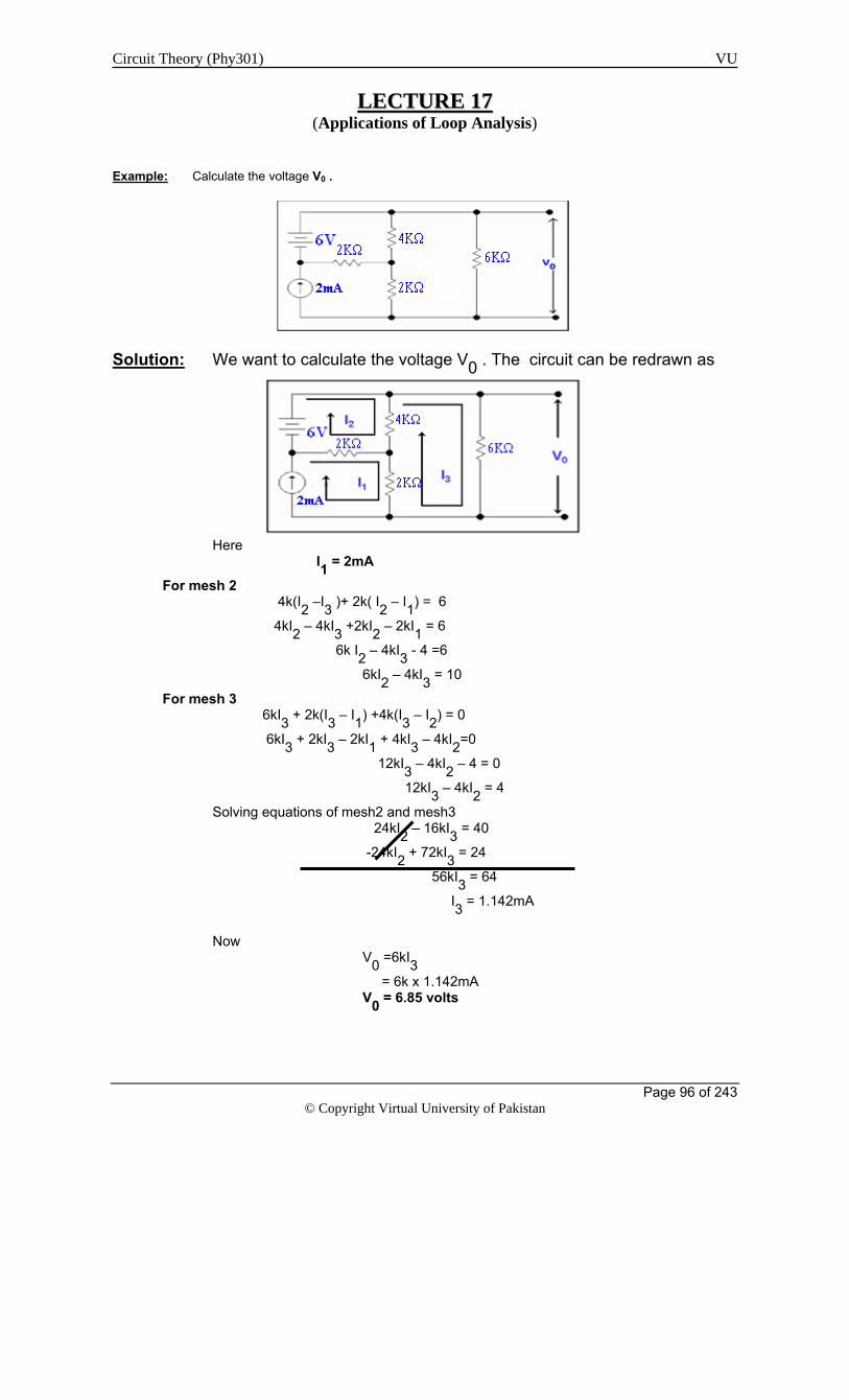
Circuit Theory (Phy301) VU
Page 96 of 243
© Copyright Virtual University of Pakistan
LLEECCTTUURREE 1177 (Applications of Loop Analysis)
Example: Calculate the voltage V0 .
Solution: We want to calculate the voltage V0 . The circuit can be redrawn as
Here I1 = 2mA
For mesh 2 4k(I2 –I3 )+ 2k( I2 – I1) = 6
4kI2 – 4kI3 +2kI2 – 2kI1 = 6
6k I2 – 4kI3 - 4 =6
6kI2 – 4kI3 = 10
For mesh 3 6kI3 + 2k(I3 – I1) +4k(I3 – I2) = 0
6kI3 + 2kI3 – 2kI1 + 4kI3 – 4kI2=0
12kI3 – 4kI2 – 4 = 0
12kI3 – 4kI2 = 4
Solving equations of mesh2 and mesh3 24kI2 – 16kI3 = 40
-24kI2 + 72kI3 = 24
56kI3 = 64
I3 = 1.142mA
Now V0 =6kI3
= 6k x 1.142mA V0 = 6.85 volts

Circuit Theory (Phy301) VU
Page 97 of 243
© Copyright Virtual University of Pakistan
Example: Calculate the voltage V0 .
Solution: We want to calculate the voltage V0 . The circuit can be redrawn as
KVL equation for mesh 1 Va + 4k(I1 – I2) =12
Va +4kI1 – 4kI2 =12
KVL equation for mesh 2 4Va +6kI2 + 4k(I2 – I1)=0
4Va +10kI2 – 4kI1 =0
Here Va =2kI1
Putting this value in the equation of mesh 1 we will get 2kI1 + 4kI1 - 4kI2 =12
6kI1 - 4kI2 =12
Now put the value of Va in the equation of mesh 2 8kI1 + 10kI2 - 4kI1 = 0
4kI1 + 10kI2 = 0
Now multiplying modified equation of mesh 1 by 1.5 and subtracting modified equation of mesh 2 from modified equation of mesh 1 6kI1 – 4kI2 = 12
– 6kI1 – 15kI2= 0
– 19kI2 =12
I2 = -12/19 mA
I2= 0.6315 mA
Now V0 = 6k x .6315
V0 = 3.78 volts

Circuit Theory (Phy301) VU
Page 98 of 243
© Copyright Virtual University of Pakistan
Example: Calculate the voltage V0 .
Solution: We want to calculate the voltage V0
. The circuit can be redrawn as
KVL equation for mesh 1 2kI1+4k(I1-Ix)-2kIx=0 6kI1 – 4kIx - 2kIx =0 I1 = Ix KVL equation for mesh 2 2kIX +4k(IX -I1)- 6 = 0 As I1 = Ix 2kIx – 6 = 0 2kIx = 6 Ix = 3mA V0 = 2kIx = 2k x 3m V0 = 6 Volts

Circuit Theory (Phy301) VU
Page 99 of 243
© Copyright Virtual University of Pakistan
LLEECCTTUURREE 1188
(Applications of Loop Analysis-super mesh technique)
Example: Calculate the voltage Vo.
Solution: We want to calculate the voltage V
o. The circuit can be redrawn as
Now Vx = (I2- I3) 6k -------------(A)
I1 = Vx/2k ---------------(B)
Put Vx from A into B we have I1 = (I2 – I3)6k/2k
= 3(I2 – I3)
Now I2 = 2mA
I1= 6mA - 3I3 Now KVL equation for mesh 3 6kI3 +6k(I3 – I2 ) +2k(I3 -I1) =0
6kI3+ 6kI3 – 12 +2kI3 -2k(6mA -3I3)=0
14kI3 – 12 -12 + 6kI3 = 0
20kI3 = 24
I3 = 1.2mA
V0 = 6kI3
= 6k(1.2mA) =7.2 volts

Circuit Theory (Phy301) VU
Page 100 of 243
© Copyright Virtual University of Pakistan
Example: Calculate the voltage Va.
Solution: We want to calculate the voltage Va.
The circuit can be redrawn as
Va can also be found by super node technique but it will take a lengthy calculation lets see how it becomes very easy with loop analysis.
Here I4 =1A
KVL for mesh 1 1(I1 – I2) +3(I1 -I3 )-5 =0
I1 – I2 +3I1 -3I3-5 = 0
4I1 – 3I3 – I2 = 5 --------(A)
KVL for mesh 2 2I2 +3I2 -2Va+I2-I1 = 0 6I2 –I1 = 2Va------(B) Va = 3I2 Put this value in (b) 6I2 –I1 = 2(3I2)
I1 = 0

Circuit Theory (Phy301) VU
Page 101 of 243
© Copyright Virtual University of Pakistan
KVL for mesh 3 2Va + 5(I3 – I4) +3(I3 –I1) =0
Putting the values of I1,I 4and Va
6I2 + 3I3 -0 +5I3 – 5 = 0
8I3 + 6I2 = 5
Solving equation for mesh 1 and mesh 3 - 18I3 - 6I2 = 30
8I3 + 6I2 = 5
-10I3 = 35
I3 = - 3.5A
Putting values of I3 and I1 in eq of mesh 1 i.e in (A) we have
10.5– I2 =5
I2= 5.5 A
As Va =3I2 Therefore Va =3 * 5.5 Va = 16.5 V Example: Find Current through all meshes.
Solution:
Incorrect approach I2=-5A
I3=+5A
We drive all these KVL equation for mesh 1 -5+I
1-I
3+2I
1=0 -------------------- (1)

Circuit Theory (Phy301) VU
Page 102 of 243
© Copyright Virtual University of Pakistan
KVL equation for super mesh 1(I3-I1)+4I2+3I2+2+4I3- 4I4+6I3=0 ------------ (2) KVL equation for Mesh 4 4I4 – 4I3+2I4-3=0 ------------ (3) Simplifying Equation (1) 3I1 - I3 = 5 Equation (2) -I1+7I2+11I3-4I4=-2 Equation (3) - 4I3 + 6I4=3 Also -I2+I3=5 Therefore I1=2.481A I2=-2.556A I3=2.444A I4=2.130A Example: Calculate current I0.
Solution: We want to calculate the current I0.
The circuit can be redrawn as

Circuit Theory (Phy301) VU
Page 103 of 243
© Copyright Virtual University of Pakistan
Here I1= -1mA I2 = -2mA KVL equation for loop 3 1k( I3 + I1 ) + 2kI3 + 1k(I3 + I2) = 2 + 4 1kI3 + 1kI1 + 2kI3 + 1kI3 + 1kI2 = 6 4kI3 – 1 – 2 = 6 4kI3 – 3 = 6 I3 = 9/4 mA I3 = 2.25 mA I3 = I0 = 2.25 mA

Circuit Theory (Phy301) VU
Page 104 of 243
© Copyright Virtual University of Pakistan
Example: Calculate current I0.
Solution: We want to calculate the current I0.The circuit can be redrawn as
Here I1 = 2mA I2= - 4mA KVL for loop 3 2kI3 + 2k(I3 + I2) = 12 2kI3 + 2kI3+ 2kI2= 12 4kI3 – 8 =12 4kI3= 20 I3 = 5mA Now I0 = I3 + I1 I0 = 5mA + 2mA = 7mA

Circuit Theory (Phy301) VU
Page 105 of 243
© Copyright Virtual University of Pakistan
LLEECCTTUURREE 1199 (Examples of Loop Analysis)
EExxaammppllee:: CCaallccuullaattee tthhee ccuurrrreenntt IIoo..
Solution: we want to calculate the current I0. The circuit can be redrawn as
Here I1 = 2mA I2 = - 4mA KVL for loop 3 2kI3 + 1k(I3 - I2) + 2k(I3 + I1 – I2) =12 2kI3 + 1kI3 -1kI2 + 2kI3 +2kI1 – 2kI2=12 5kI3 -3kI2 + 2kI1= 12 5kI3 + 12 + 4 = 12 5kI3= - 4 I3 = - 4/5 mA I3 = .8mA Now I0 = I3 + I1- I2 = -.8 +2 +4 I0 = 5.2 mA

Circuit Theory (Phy301) VU
Page 106 of 243
© Copyright Virtual University of Pakistan
Example: Calculate the voltage V0.
Solution: we want to calculate the voltage V0. The circuit can be redrawn as
Here I1= -2mA I2= - 4mA I3= 4mA KVL for loop 4 1k(I4 – I1) + 1k(I4- I2) + 1kI3 + 2kI4 = 12 1kI4 – 1kI1 + 1kI4 – 1kI2 +1kI3 +2kI4 = 12 4kI4 + 2 + 4 + 4 =12 I4 = 2/4k I4 = 0.5 mA Now current through 1k resistor I1k = I4 – I1 = 0.5 – (-2) I1k = 2.5mA V0 = 1k x 2.5m V0 =2.5 volts

Circuit Theory (Phy301) VU
Page 107 of 243
© Copyright Virtual University of Pakistan
Example: Calculate the voltage V0.
Solution: we want to calculate the voltage V0. The circuit can be redrawn as
Here I1= 4mA I2= - 2mA I3= 1mA KVL for loop 4 1k(I4 – I1) + 1k(I4- I2+I3) + 2k(I4+I3) +1kI4 = 0 1kI4 – 1kI1 + 1kI4 – 1kI2 +1kI3 +2kI3+ 2kI4+1kI4 = 0 5kI4 – 4 +1+2+2 =0 5kI4 = -1
I4 = -0.2 mA Now V0 = 2k(I4 + I3 ) =2k( -0.2 +1) V0 = 1.6 volts

Circuit Theory (Phy301) VU
Page 108 of 243
© Copyright Virtual University of Pakistan
LLEECCTTUURREE 2200 (Super Mesh Technique - Coupling equation)
Example: Calculate the voltage Vo.
Solution: we want to calculate the voltage V0. The circuit can be redrawn as
Here I1 = - 2mA KVL equation for loop 2 2kI2 + 4kI2 + 2k(I2 + I1) = 12 6kI2 + 2kI2 + 2kI1 = 12 8kI2 – 4 = 12 8kI2 = 16 I2 = 2mA Now Vo = 2k(I2) = 2k (2m) Vo = 4 volts

Circuit Theory (Phy301) VU
Page 109 of 243
© Copyright Virtual University of Pakistan
Example: Calculate the voltage Vo.
Solution: We want to find the voltage V0. The circuit can be redrawn as
Here I1 =3mA I2 = 1mA KVL for loop 3 4kI3 + 2k(I3 +I2) + 4k(I3 –I1) +2k(I3 – I1) =6 4kI3 +2kI3 +2kI2 +4kI3 – 4kI1 +2kI3 -2kI1=6 12kI3 +2 -12 – 6 =12 12kI3 =22 I3 =11/6mA I3=1.833mA V0 = 4kI3 = 4k x 1.833m V0= 7.33 volts

Circuit Theory (Phy301) VU
Page 110 of 243
© Copyright Virtual University of Pakistan
Example: Calculate the current Io.
Solution: We want to find the current Io.
The circuit can be redrawn as
Here I1 =-2mA I3 = 1mA Now KVL for mesh 2 4k(I2 +I4 ) +2k(I2 – I3) +2k(I2 – I1) =0 8kI2 +4kI4 – 2 +4 =0 4kI2 +2kI4 = -1 Now KVL for loop 4 4k(I4 +I2) +2k(I4 +I3 ) +6kI4 -6 =0 12kI4 +4kI2 +2 -6 =0 12kI4 +4kI2 -4 =0 3kI4 +1kI2 =1 Multiplying equation of mesh2 by 3 and equation of loop 4 by 2 and subtracting 12kI2 +6kI4 = -3 -2kI2 -6kI4 = -2 10kI2 =-5 I2 = -o.5mA Now I0 = I1 – I2 I0= -2 +0.5 So I0 = -1.5mA

Circuit Theory (Phy301) VU
Page 111 of 243
© Copyright Virtual University of Pakistan
Example: Find the currents I1,I2 and I3.
Solution: We want to find the currents I1,I2 and I3.. The circuit can be redrawn as
For mesh 1 4I
1 -4I
2 +1 = 0 ...............(1)
For Super mesh (mesh 2 and mesh 3) 3I2 + 2I3 + 4I2 - 4I1 = 0 ...............(2) Coupling Equation I3 - I2 = 2 VX
Here VX = 3I2 Solving equation 1 4I1 - 4I2 = -1 Solving equation 2
- 4I1 + 7I2 + 2I3 = -1
For Mesh 3 -7I2 + I3 = 0 --------------(3) Solving equation 1,2 and 3 I1 = - 308.8 mA I2 = - 58.82 mA I3= - 411.8 mA

Circuit Theory (Phy301) VU
Page 112 of 243
© Copyright Virtual University of Pakistan
LLEECCTTUURREE 2211 (Examples of Loop Analysis by using dependent sources - Coupling equation)
EExxaammppllee:: CCaallccuullaattee tthhee vvoollttaaggee VVoo..
Solution: we want to calculate the voltage V0.
The circuit can be redrawn as
V
0 can be given as
V0 = 2k(I
1 +I
2)
Now I
1 = 2V
0/1k
= 2(2k(I1
+I2))/1k
= 4(I1 +I
2)
I1 = 4I
1 +4I2
-3I1
= 4I2
I1 = -4/3 I
2 Now KVL for loop 2 4kI
2 +4k(I
1 +I
2 ) +2k(I
1 +I
2) =6
4kI2 +4kI
1 +4kI
2 +2kI
1 +2kI
2 = 6
10kI2 +6kI
1 =6
5kI2 +3kI
1 =3
We know I
1 =-4/3 I
2 So 5kI
2 +3k(-4/3)I
2 = 3
5kI2 - 4kI
2 =3
I2 = 3mA
So I
1 = (-4/3) I
2

Circuit Theory (Phy301) VU
Page 113 of 243
© Copyright Virtual University of Pakistan
I1 =-4mA
Now V
0 = 2k(I
1 +I
2)
= 2k(-4m + 3m) V0 =-2 volts
Example: Calculate the voltage Vo.
Solution: We want to find the voltage V0.
The circuit can be redrawn as
Here I2 = -4mA
I3 =-1mA
Now Vx = -(I
3 +I
4)1k
and I
1 = 2Vx/1k
I1 = -2(I
3 +I
4)
= 2 - 2I4
Now KVL for loop4 -1k(I4 +I3) +1k(I4 +I3) +1k(I4 +I3 –I2) +1k(I4- I1) +2kI4 = 0
2kI4 – 2 -1kI
4 +1 +4 +2kI
4 +1k(I
4 -2 +2I
4)= 0
6kI4 +1 = 0
6kI4 = -1
I4 =-1/6k
Now V
0 = 1k(I
4 + I
3)
= 1k( -1/6 – 1) = 1k(-.166 -1) V0= -1.166 volts

Circuit Theory (Phy301) VU
Page 114 of 243
© Copyright Virtual University of Pakistan
Example: Find loop currents.
Solution: We use the coupling equation technique to find loop currents to find the loop currents. The KVL equation for this supermesh -7 +1(I1 –I2) +3(I3 –I2) +1I3 =0
I1 -4I
2 +4I
3 =7 (1)
And for mesh2 1(I2 –I1)) +2I2 +3(I2 – I3) =0
-I1 +6I
2 -3I
3 =0 (2)
Coupling equation I1 –I3 = 7 (3)
solving (1) and (2) 6I
1 -24I
2 +24I
3 = 42
-4I1 +24I
2 -12I
3 = 0
2I
1 +12I
3= 42 (4)
Subtracting (3) and (4) 2I
1 +12I
3 = 42
2I1 - 2I
3 = 14
14I
3 = 28
I3 =2 A
putting this in (1) I
1 -2 =7
I1 =9A
and hence I2 can be calculated by putting I
1 and I
2 in (1) or (2)
from 1 9 – 4I
2 +8 =7
-4I2 = -17+7
4I2 =10
I2 =2.5A

Circuit Theory (Phy301) VU
Page 115 of 243
© Copyright Virtual University of Pakistan
LLEECCTTUURREE 2222 (Matrices and determinants)
MATRICES AND DETERMINANTS are the coefficients of the independent variables. a
ij may be constant or functions of some parameter. A
more convenient form may be obtained for the above equations by expressing them in matrix form
11 12 13 1n1 1
21 22 23 2n2 2
m nm1 m2 m3 mn
a + a + a + ...... + ay xa + a + a + ...... + ay x
.... ..............................................y xa + a + a + ........+ a
⎡ ⎤⎡ ⎤ ⎡ ⎤⎢ ⎥⎢ ⎥ ⎢ ⎥⎢ ⎥⎢ ⎥ ⎢ ⎥=⎢ ⎥⎢ ⎥ ⎢ ⎥⎢ ⎥⎢ ⎥ ⎢ ⎥
⎣ ⎦ ⎣ ⎦⎣ ⎦
Or Y = A X Matrix A=[aij] is called the characteristic matrix of the system; its order or dimension is denoted as
d(A) =m x n where m is the number of rows and n is the number of columns. Attached to any matrix A=[aij] is a certain scalar function of the a
ij, called the determinant of A. This
number is denoted as det A or |A| or ∆A or
a11 +a12 +a13+ … +a1n a21 +a22 +a23 + …+a2n
……………………… am1 +am2+am3+…+amn
Applying these concepts to our analysis, the solution of simultaneous equations becomes very easy. Lets take some examples of KVL and KCL and apply this technique and we will see that the simplification of our equations will become extremely easy. Example: Find current I0.By using matrices
Solution: KCL at node 1 βI
0 + V1/R1 + (V1 – V2)/R2 =0 ------------ (1)
KCL at node 2 (V2 – V1)/R2 +I
0 –Ia =0 ------------- (2)
Where Io =V2/R3 ------------------(A)
Simplifying these equations for node 1 and 2 put the value of equation A in 1 and 2 we have

Circuit Theory (Phy301) VU
Page 116 of 243
© Copyright Virtual University of Pakistan
β V
2/R
3 + V
1/R
1 + V
1/R
2 – V
2/R
2 = 0
(1/R1 +1/R
2) V
1 – (1/R
2 - β /R
3) V
2 = 0
For node 2 -(1/R
2) V1 + (1/R
2 +1/R
3 )V
2 =I
a Or in matrix form
1 2 2 3 1
a2 2 3 2
(1/R + 1/R ) -(1/R - ß /R ) V 0I -1/R (1/R + 1/R ) V
⎡ ⎤ ⎡ ⎤ ⎡ ⎤=⎢ ⎥ ⎢ ⎥ ⎢ ⎥
⎣ ⎦⎣ ⎦⎣ ⎦
Now lets determine the node voltage for the following given parameters β =2, R
2 =6k, R
1=12k, R
3=3k, I
a =2mA
Using these equations for the network yields (1/4k) V1 +(1/2k) V2 = 0 -(1/6k) V1 +(1/2k) V2 =2 m A Or in matrix form
1
2
V1/4k 1/2k 0-1/6k 1/2k V 2m
⎡ ⎤⎡ ⎤ ⎡ ⎤=⎢ ⎥⎢ ⎥ ⎢ ⎥
⎣ ⎦ ⎣ ⎦⎣ ⎦
The circuit equations can be solved using matrix analysis. The general form of matrix equation is A X = Y or GV=I we want to find X or V
where in this case V or X = 1
2
VV
⎡ ⎤⎢ ⎥⎣ ⎦
, G or A =1/4k 1/2k-1/6k 1/2k
⎡ ⎤⎢ ⎥⎣ ⎦
and I or Y= 02m
⎡ ⎤⎢ ⎥⎣ ⎦
The solution of the matrix equation is X = A-1 Y OR V = G-1 I ---------(B) To find A-1or G-1 We know that A-1 = Adj(A) / |A| or G-1 = Adj(G) / |G| Adjoint of the coefficient matrix A is
1/2k -1/2k
Adj(A)1/6k 1/4k
⎡ ⎤= ⎢ ⎥
⎣ ⎦
And the determinant will be | A | = (1/4k)(1/2k) - (1/6k)(-1/2k)
= 5/24k2
A-1 = Adj(A) / |A|
1
2
1/2k -1/2k1/6k 1/4k
A 524k
−
⎡ ⎤⎢ ⎥⎣ ⎦=
by putting A-1 in equation (B) we have
Therefore
1 2
2
V 1/2k -1/2k 0= 24k /5
V 1/6k 1/4k 2m⎡ ⎤ ⎡ ⎤ ⎡ ⎤⎢ ⎥ ⎢ ⎥ ⎢ ⎥
⎣ ⎦ ⎣ ⎦⎣ ⎦

Circuit Theory (Phy301) VU
Page 117 of 243
© Copyright Virtual University of Pakistan
21
2
21
2
1
2
V (1/2k)(0) + (-1/2k)(2m)24kV (1/6k)(0) + (1/4k)(2m)5
0 - 1V 24k1V 5 0+2
24V 5V 12
5
⎡ ⎤ ⎡ ⎤=⎢ ⎥ ⎢ ⎥
⎣ ⎦⎣ ⎦⎡ ⎤⎡ ⎤ ⎢ ⎥=⎢ ⎥ ⎢ ⎥⎣ ⎦ ⎣ ⎦
⎡ ⎤−⎢ ⎥⎡ ⎤= ⎢ ⎥⎢ ⎥
⎣ ⎦ ⎢ ⎥⎢ ⎥⎣ ⎦
Hence V1 = -24/5V V2 =12/5 V Hence I
o
I0
= V2/R3
=(12/5)/3k =4/5k = 4/5mA I0= 0.8mA
Example: Find current I1 , I2and I3.By using matrices.
Solution: We want to calculate the currents I1 ,I2 and I3. By using matrices proceed as
KCL at node 1 -1m +(1/12k)(V1 – 0) + (1/6k)(V1 – V2)=0 (1/12k + 1/6k)V1 – (1/6k) V2 =1mA -------------(A) KCL for node 2 -(1/6k)(V1 – V2) +4m + (1/6k)(V2 -0 )=0 Which can be expressed as -(1/6k)V1 +(1/6k + 1/6k) V2 = - 4mA --------- (B) Simplifying these two equations (A) and (B) V1/4k - V2/6k = 1mA -V1/6k + V2/3k = -4mA Or in matrix form

Circuit Theory (Phy301) VU
Page 118 of 243
© Copyright Virtual University of Pakistan
1
2
V 1/4k -1/6k 1m
-1/6k 1/3k V 4m⎡ ⎤⎡ ⎤ ⎡ ⎤
=⎢ ⎥⎢ ⎥ ⎢ ⎥−⎣ ⎦ ⎣ ⎦⎣ ⎦
The circuit equations can be solved using matrix analysis. The general form of matrix equation is A X = Y or GV=I we want to find X or V
where in this case V or X = 1
2
VV
⎡ ⎤⎢ ⎥⎣ ⎦
, G or A =1/4k -1/6k-1/6k 1/3k
⎡ ⎤⎢ ⎥⎣ ⎦
and I or Y=1m
4m⎡ ⎤⎢ ⎥−⎣ ⎦
The solution of the matrix equation is X = A-1 Y OR V = G-1 I --------- (C) To find A-1or G-1 we know that A-1 = Adj(A) / |A| or G-1 = Adj(G) / |G| Ad joint of the coefficient matrix A is
Adj (A) =1/3k 1/6k1/6k 1/4k
⎡ ⎤⎢ ⎥⎣ ⎦
And the determinant will be | A| =(1/3k)(1/4k) - (-1/6k)(-1/6k)
= 1/18k2
A-1 = Adj(A) / |A|
1
2
1/3k 1/6k1/6k 1/4k
A 118k
−
⎡ ⎤⎢ ⎥⎣ ⎦=
by putting A-1 in equation (C) we have
1 2
2
V 1/3k 1/6k 1m= 18k
V 1/6k 1/4k -4m⎡ ⎤ ⎡ ⎤ ⎡ ⎤⎢ ⎥ ⎢ ⎥ ⎢ ⎥
⎣ ⎦ ⎣ ⎦⎣ ⎦
By solving the above equation we have
1
2
V -6 =
V -15⎡ ⎤ ⎡ ⎤⎢ ⎥ ⎢ ⎥
⎣ ⎦⎣ ⎦
Hence V1 = - 6V V2 =- 15 V Knowing the voltages we can determine all currents using OHM’s LAW I
1 = V1/12k
=-6/12k =-1/2mA I1 =-0.5mA
Now I2
can be calculated as
I2 = (V1 – V2)/6k
= -6 – (-15)/6k I2= 3/2mA
Now for I3
I3 = V2/6k
= -15/6k I3= - 5/2mA

Circuit Theory (Phy301) VU
Page 119 of 243
© Copyright Virtual University of Pakistan
LLEECCTTUURREE 2233 (Superposition Theorem and examples)
Example: Find current I1 , I2 and I3 By using Cramer’s rule.
Solution: We will use Cramer’s rule to solve this example KVL equation for loop 1 2I1 + 5( I1 – I2) = -25
2I1 +5I
1 – 5I
2 =-25
7I1 – 5I
2 = -25 ----------------- (A)
KVL equation for loop 2 10I2 + 4(I2 – I3) + 5(I2 – I1) = 25
10I2 + 4I
2 – 4I
3 + 5I
2 – 5I
1 = 25
-5I1 + 19I
2 – 4I
3 = 25 ---------------- (B)
KVL equation for loop 3 2I3 + 4(I3 – I2) = 50
2I3 + 4I
3 – 4I
2 = 50
-4I2 + 6I
3 = 50 --------------- (C)
We will write equation A ,B and C In matrix form
1
2
3
I7 -5 0 -25 -5 19 -4 I 250 -4 6 50I
⎡ ⎤⎡ ⎤ ⎡ ⎤⎢ ⎥⎢ ⎥ ⎢ ⎥=⎢ ⎥⎢ ⎥ ⎢ ⎥⎢ ⎥⎢ ⎥ ⎢ ⎥⎣ ⎦ ⎣ ⎦⎣ ⎦
The determinant of the coefficient matrix is
| A | =
7 -5 0-5 19 -40 -4 6
A = 536
By Cramer’s rule
1
-25 -5 0 7 -5 0I 25 19 -4 ÷ -5 19 -4
50 -4 6 0 -4 6=
I
1 = (-700) ÷ 536
I1= -1.31 A
By Cramer’s rule

Circuit Theory (Phy301) VU
Page 120 of 243
© Copyright Virtual University of Pakistan
2
7 -25 0 7 -5 0I -5 25 -4 ÷ -5 19 -4
0 50 6 0 -4 6=
I
2 = 1700/536
I2 = 3.17A
By Cramer’s rule
3
7 -5 -25 7 -5 0I -5 19 25 ÷ -5 19 -4
0 -4 50 0 -4 6=
I
3 = 5600/536
I3 = 10.45 A
Superposition Theorem : The principle of superposition, which provides us with the ability to reduce a complicated problem to several easier problems – each containing only a single independent source – states that “In any linear circuit containing multiple sources, the current or voltage at any point in the circuit may be calculated as the algebraic sum of the individual contributions of each source acting alone.” When determining the contributions due to independent sources, any remaining current sources are made zero by replacing them by open circuit and any voltage sources are made zero by replacing them by short circuit. Example: Calculate Vo by applying principle of superposition.
Solution: Applying principle of superposition, we will take effect of the sources one by one. Only voltage source is acting
Applying voltage division rule
1 1R1
1 2
R VVR R
×=
+
V
01 = V
6k = (6 x3)/3+6
V01 =2 volts

Circuit Theory (Phy301) VU
Page 121 of 243
© Copyright Virtual University of Pakistan
Only current source is acting
Let the current through 6k resistor is I
0 by applying current division rule
2R1
1 2
R I(t)IR R
×=
+
I
0 = (3 x 2)/9 = 2/3 mA
V02
= I0 x 6k
=2/3m x 6k = 4V So V
0 will be
V0 = V
01 + V
02
= 2V + 4V V0 = 6V
Example: Calculate Vo by applying principle of superposition.
Solution: We want to calculate the voltage V
0. Superposition theorem can be applied as
Only current source is acting
Let I
0 be the current following through the 6k resistor then
2kII4k=(2x4)/(2+4)=8/6=(4/3)k (4/3)k is in series to 2k ∴ (4/3)k+2kII6k, hence applying current division rule
2R1
1 2
R I(t)IR R
×=
+

Circuit Theory (Phy301) VU
Page 122 of 243
© Copyright Virtual University of Pakistan
(4 / 3) 2 20 202(4 / 3 2) 6 3(28 / 3) 28oI mA+
= = =+ +
0120 30V 6 V28 7
= =
Making only voltage source to act
Or it can be redrawn as
ab8x4 8R 8k 4k k8 4 3
= = =+
ab
8 k 243V 68 7k 2k3
= =+
0224 6k 18x Volts.7 6k 2k 7
V = =+
o o1 o230 18 48V V V Volts7 7 7
= + = + =
Example: Calculate Vo by applying principle of superposition.
Solution: We want to calculate Vo. When only voltage source is acting
Applying voltage division rule
1 1R1
1 2
R VVR R
×=
+
V01=(12x2)/(7+2)=24/9V

Circuit Theory (Phy301) VU
Page 123 of 243
© Copyright Virtual University of Pakistan
When only current source is acting
Let Io flows through 2kΩ. applying current division rule
2R1
1 2
R I(t)IR R
×=
+
Io=(-2)3/(6+3)=-6/9=-2/3mA
Vo2= 2x-2/3=-4/3 Volts
Therefore, Vo=Vo1+Vo2 =24/9 – 4/3 Vo =4/3 Volts
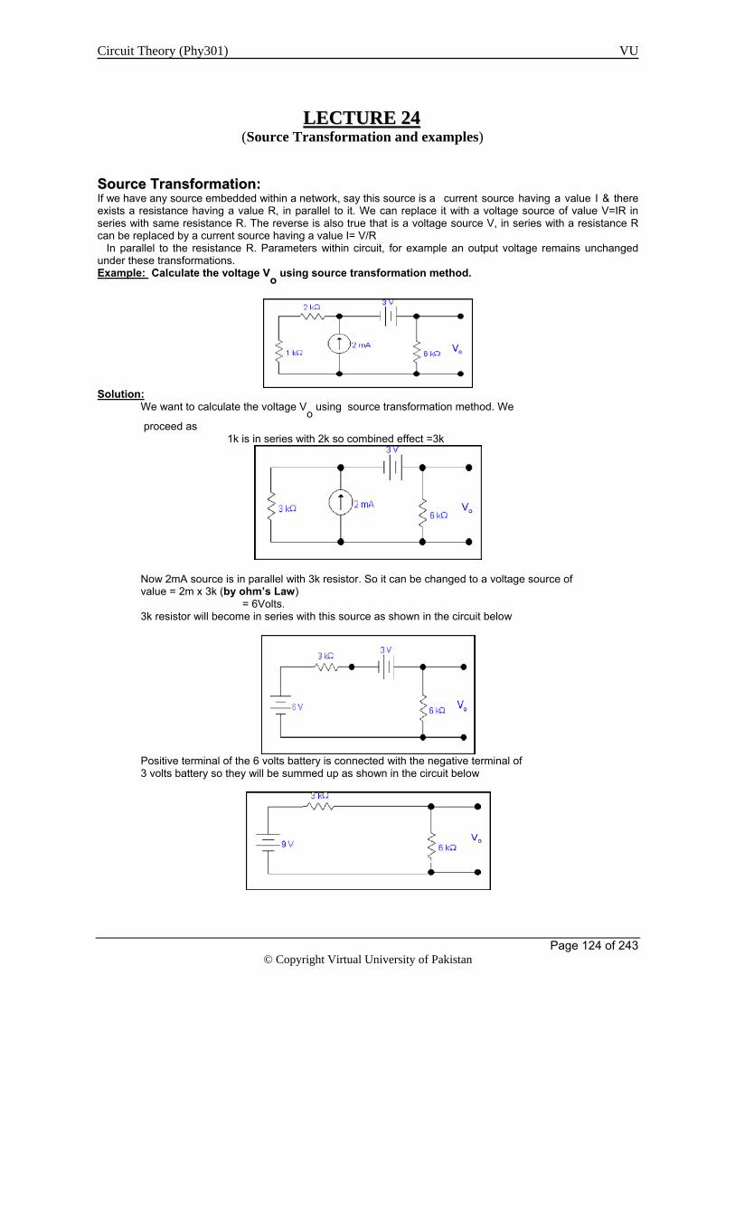
Circuit Theory (Phy301) VU
Page 124 of 243
© Copyright Virtual University of Pakistan
LLEECCTTUURREE 2244 (Source Transformation and examples)
SSoouurrccee TTrraannssffoorrmmaattiioonn:: If we have any source embedded within a network, say this source is a current source having a value I & there exists a resistance having a value R, in parallel to it. We can replace it with a voltage source of value V=IR in series with same resistance R. The reverse is also true that is a voltage source V, in series with a resistance R can be replaced by a current source having a value I= V/R In parallel to the resistance R. Parameters within circuit, for example an output voltage remains unchanged under these transformations. Example: Calculate the voltage Vo using source transformation method.
Solution: We want to calculate the voltage V
o using source transformation method. We
proceed as 1k is in series with 2k so combined effect =3k
Now 2mA source is in parallel with 3k resistor. So it can be changed to a voltage source of value = 2m x 3k (by ohm’s Law) = 6Volts. 3k resistor will become in series with this source as shown in the circuit below
Positive terminal of the 6 volts battery is connected with the negative terminal of 3 volts battery so they will be summed up as shown in the circuit below

Circuit Theory (Phy301) VU
Page 125 of 243
© Copyright Virtual University of Pakistan
Applying voltage division rule
1 1R1
1 2
R VVR R
×=
+
Vo = (6 x 9)/9
= 6 Volts Example: Calculate the voltage Vo using source transformation method.
Solution: We want to calculate the voltage V
o using source transformation method. We
proceed as 3k is in series with 12 volts battery. So it can be converted into a current source of value =12/3k (by ohm’s Law) =4mA Now voltage source has transformed in the current source as shown below
Now 3k resistor is in parallel with 6k resistor so 3k||6k = (3k x6k)/3k +6k = 2k Now we will replace 3k and 6k resistance with 2k as shown in the circuit below
4mA source is parallel with 2k resistor. So it can be converted into a voltage source. By using ohm’s Law we have the value of voltage source = 8 volts which is in series with a resistor of 2k, so our modified circuit will be
In the above circuit 2k is in series with 2k so modified circuit will be

Circuit Theory (Phy301) VU
Page 126 of 243
© Copyright Virtual University of Pakistan
8V source is in series with 4k resistor. So it can be converted into a current source of value = 8/4k (by using Ohm’s Law) = 2mA 2mA current source is in parallel to 4k Our modified circuit will be as
In the above circuit two current sources are parallel to each other, so current sources will add up to give value of 4mA. Our modified circuit will be as
In the above circuit 4mA source is in parallel with 4k resistor .So it can be converted into a voltage source of value 16volts by Ohm’s Law. Our modified circuit will be as
In the above circuit 4k and 4k are in series so our modified circuit will be
Now applying voltage division rule
1 1R1
1 2
R VVR R
×=
+
V0 = 8k/16k x 16V
V0 = 8volts

Circuit Theory (Phy301) VU
Page 127 of 243
© Copyright Virtual University of Pakistan
Example: Calculate the voltage Vo using source transformation method.
Solution: We want to calculate the voltage V
o using source transformation method. We
Proceed as 12 volt source is in series with 3k resistor. So it can be converted into current source of value I = 12/3k =4mA (by Ohm’s Law) In modified circuit 4mA current source and resistor 3k will be in parallel. So modified circuit will be as
Now we will combine current sources as 4m – 2m = 2mA, so our modified circuit will be as,
2mA source is in parallel with 3k source so it can be converted into a voltage source of value V=2 x3 = 6volts (by Ohm’s Law) Our modified circuit will be as,
In the above circuit 3k is in series with 4k so modified circuit will be as
Now applying voltage division rule

Circuit Theory (Phy301) VU
Page 128 of 243
© Copyright Virtual University of Pakistan
1 1R1
1 2
R VVR R
×=
+
V0 = 2k/9k x 6
=12/9 V0 = 4/3 volts
Example: Calculate the current I using source transformation method.
Solution: we want to calculate the current I by source transformation.
3 Ohms resistor is in parallel with 5A source. So it can be converted into a voltage source 15V.
3 Ohms resistor 4 Ohms are in series and the resultant is in series with 15V so it can be converted into a current Source.
7|| 7 = 7 x 7 / 7+ 7 =49/14 = 3.5 ohm

Circuit Theory (Phy301) VU
Page 129 of 243
© Copyright Virtual University of Pakistan
Current source is in parallel with 3.5 ohms resistance. So it can be converted into a Voltage source by using Ohm’s Law V =IR= 15/7 X 3.5 = 7.5 Volts
The current I can be found using KVL -7.5 + 3.5I – 51V
x + 28I +9 =0 -------------- (A)
Where Vx = 2I
putting the value of Vx in (A) we have
-7.5 + 3.5 I - 51(2I) + 28I +9 = 0 3.5I -102I +28I + 1.5 = 0 -70.5I +1.5 = 0 I = 1.5/70.5 I = 21.28mA

Circuit Theory (Phy301) VU
Page 130 of 243
© Copyright Virtual University of Pakistan
LLEECCTTUURREE 2255 (Thevenin's Theorem) THEVENIN’S THEOREM:
In solving any problem by Thevenin’s theorem. We will follow the steps as stated below (1) First of all we will remove the load resistor( The resistor we want to calculate the unknown quantity
that is voltage, current or power) from the circuit leaving behind an open circuit. (2) Calculating the V
th at open terminals of the open circuit by any method.
(3) Calculating the Rth
(The total resistance in the Thevenin’s circuit) by open circuiting all
current sources and short circuiting all voltage sources. (4) After calculating V
th and R
th, re-inserting the load resistance R
L in the circuit in series with R
th and
considering the Vth
as a battery in series with these two resistances.
Example: Calculate the voltage Vo by using Thevenin’s theorem .
Solution: We want to calculate V0 by using Thevenin’s theorem .we will follow the
steps given earlier. First step: Removing RL
Here R
L is 6k resistor at which we want to calculate the voltage V
o. Second step: Calculating Vth
1k is in series with 2k so modified circuit will be as
3k is in parallel with 2mA source, so by source transformation Now 2mA source is in parallel with 3k resistor.So it can be changed to a voltage source of value = 2m x 3k (by ohm’s Law) = 6 Volts. 3k resistor will become in series with this source as shown in the circuit below
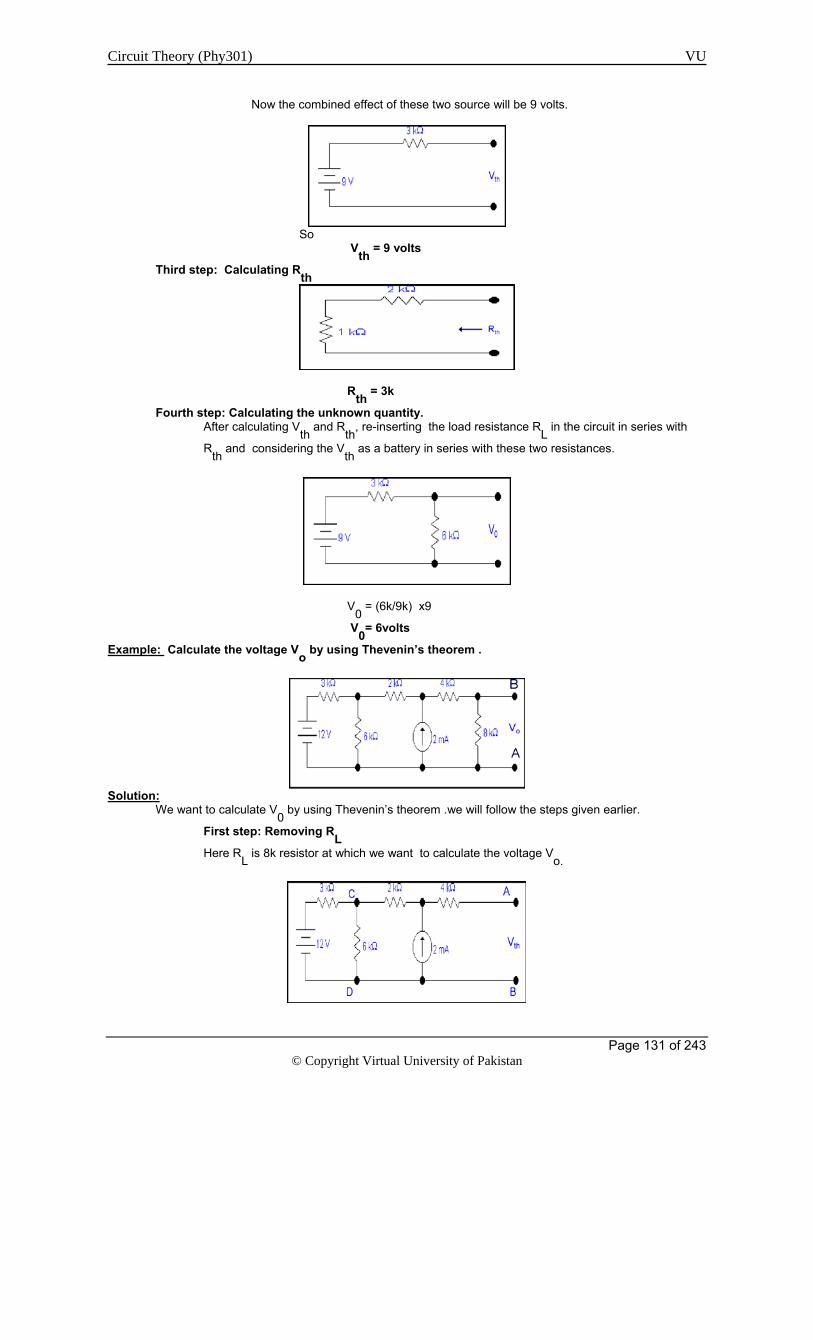
Circuit Theory (Phy301) VU
Page 131 of 243
© Copyright Virtual University of Pakistan
Now the combined effect of these two source will be 9 volts.
So Vth = 9 volts
Third step: Calculating Rth
Rth = 3k
Fourth step: Calculating the unknown quantity. After calculating V
th and R
th, re-inserting the load resistance R
L in the circuit in series with
Rth
and considering the Vth
as a battery in series with these two resistances.
V
0 = (6k/9k) x9
V0= 6volts
Example: Calculate the voltage Vo by using Thevenin’s theorem .
Solution: We want to calculate V
0 by using Thevenin’s theorem .we will follow the steps given earlier.
First step: Removing RL Here R
L is 8k resistor at which we want to calculate the voltage V
o.

Circuit Theory (Phy301) VU
Page 132 of 243
© Copyright Virtual University of Pakistan
Second step: Calculating Vth
Now we will follow the superposition method to calculate Vth.
Only voltage source is acting
No current in ‘CA’ branch so voltage drop across 4k and 2k resistor is zero so VCD = Vth1 Applying voltage division rule V
CD =V
th1 =V
6k =(12 x6)/(3+6)
= 8 volts Only current source is acting
3k||6k = (3k x6k)/(3k+6k) =2k 2k is in series with 2k =4k
Current through open circuit is zero by ohm’s law so V
th2 = 4k x2m
Vth2= 8 volts
So V
th = V
th1 +V
th2
= 8 +8 V
th = 16 volts

Circuit Theory (Phy301) VU
Page 133 of 243
© Copyright Virtual University of Pakistan
Third step: Calculating Rth
3k||6k = (3k x6k)/9k = 2k
R
th = 2k+2k+4k
Rth = 8k
Fourth step: Calculating unknown quantity. After calculating V
th and R
th, re-inserting the load resistance R
L in the circuit in series with
Rth
and considering the Vth
as a battery in series with these two resistances.
V
0 = (8k/16k) x16
V0= 8 volts
Example: Calculate the voltage Vo by using Thevenin’s theorem .
Solution: We want to calculate V
0 by using Thevenin’s theorem .we will follow the steps given earlier.
First step: Removing RL Here R
L is 6k resistor at which we want to calculate the voltage V
o.

Circuit Theory (Phy301) VU
Page 134 of 243
© Copyright Virtual University of Pakistan
Second step: Calculating Vth
Apply KVL to the circuit Here I
2 = 2mA
For loop 1 4kI
1 +2k( I
1 –I
2) = 6
4kI1 +2kI
1 – 2kI
2 =6
6kI1 -2kI
2 =6
Putting value of I2
6kI1 – 4 =6
I1 = 10/6k
I1 =1.6mA
Now voltage across 4k resistor V
4k = 1.6m x4k=20/3
V4k = 6.66volts
Voltage across 2k resistor V
2k = 2m x2k
V2k = 4volts
So V
th = V4k +V2k
=20/3 + 4 = 6.66 +4 Vth =10.66 volts
Third step: Calculating Rth
4k||2k = 4k x2k/6k =8/6 k =4/3 k=1.33 k
They are in series so Rth=1.33k +2k=10/3k Rth =3.33k

Circuit Theory (Phy301) VU
Page 135 of 243
© Copyright Virtual University of Pakistan
Fourth step: Calculating unknown quantity. After calculating V
th and R
th, re-inserting the load resistance R
L in the circuit in series with
Rth
and considering the Vth
as a battery in series with these resistances.
V
0 = 32/3 x6 x 1/(10/3+6 )
= 64 x3/10 +18 =192/28 V0= 48/7 volts

Circuit Theory (Phy301) VU
Page 136 of 243
© Copyright Virtual University of Pakistan
LLEECCTTUURREE 2266 (Examples of Thevenin's Theorem - Thevenin's Theorem and Dependent sources with examples)
Example: Calculate the voltage Vo by using Thevenin’s theorem .
Solution: We want to calculate V0 by using Thevenin’s theorem .we will follow the
following steps . First step: Removing RL
Here R
L is 4k resistor at which we want to calculate the voltage V
o. Second step: Calculating Vth
We want to calculate V
th .
Apply KVL in two loops to calculate the individual loop
currents.
Here I1 = 2mA

Circuit Theory (Phy301) VU
Page 137 of 243
© Copyright Virtual University of Pakistan
KVL for the super mesh -6 +6kI
2 +12k(I
1 +I
2) + 12k(I
1 +I
2) =0
-6 +6kI2 +12kI
2 + 12kI
2 +24kI
1 =0
30kI2 – 6 +24k(2m)=0
30KI2 -6 +48 =0
I
2 = -42/30mA
I2= -1.4mA
Now we will calculate the voltage across 6k and 12 k to find the value of Vth Therefore, V
6k = 6kI
2 = 6k(-1.4m) V6k = -8.4volts
V12k
= 12k(I1 +I2)
= 12k( 2m -1.4m) V12k = 7.2volts
So, V
th = V6k + V12k
= -8.4 +7.2 Vth = -1.2volts
Third step: Calculating Rth
6k is in series with 12k .The resultant of these two is in parallel with 12k. (6k+12k)||12k = 18k x12k/(12k+18k) Rth = 7.2k
Fourth step: Calculating the unknown quantity. After calculating V
th and R
th, re-inserting the load resistance R
L in the circuit in series with
Rth
and considering the Vth
as a battery in series with these two resistances.
V
0 = -1.2 x4k/(7.2k + 4k)
V0 = - 0 .4285 volts

Circuit Theory (Phy301) VU
Page 138 of 243
© Copyright Virtual University of Pakistan
Example: Calculate the value of RL and the maximum power dissipation across it by Thevenin’s Theorem.
Solution: We want to calculate R
L and the maximum power across it by using Thevenin’s theorem .we will follow
the steps given earlier. First step: Removing RL
To remove R
L to calculate V
th .In this case our R
th is our R
L.
Second step: Calculating Vth
We want to calculate Vth
. Apply KVL in two loops to calculate the individual loop
currents.
Here I
1 = 2mA
Applying KVL to loop 2 6kI
2 + 3k(I
2 – I
1) +3 =0
9kI2 -3kI
1 + 3 =0
9kI2 – 6 +3 =0
I2 = 1/3 mA
I2 = 0.33mA
Now we will calculate the voltage across 4k and 6k to find the value of Vth Therefore, V
AB = 4k(I
1)
= 4k( 2m) VAB = 8 volts
VBC
= 6k(I2)
= 6k x 0.33m VBC = 2 volts
So V
th = V
AB + V
BC = 8 +2 Vth = 10 volts

Circuit Theory (Phy301) VU
Page 139 of 243
© Copyright Virtual University of Pakistan
Third step: Calculating Rth
To calculate Rth .
Short circuiting the voltage source and open circuiting the current source.
3k is in parallel with 6k and 4k is series with these two so
3k||6k + 4k = 3k x 6k/(3k + 6k) +4k = 2k +4k = 6k = R
th =R
L Rth =RL= 6k
Fourth step: Calculating unknown quantity. After calculating V
th and R
th, re-inserting the load resistance R
L in the circuit in series with
Rth
and considering the Vth
as a battery in series with these two resistances.
For maximum power dissipation R
L =R
th = 6k
PL = I
2R ------------- (A)
From Ohm’s law V=IR and I = V/R so I =10/12 put in A we have
PL = (10/12k)
2 (6k)
= (0.83) 2
X 6 PL= 4.1 mW
Example: Calculate the value of RL and the maximum power dissipation across it by Thevenin’s Theorem.
Solution: We want to calculate R
L and the maximum power across it by using Thevenin’s theorem .we will follow
the following steps . First step: Removing RL To remove R
L to calculate V
th .In this case our R
th is our R
L.
Second step: Calculating Vth

Circuit Theory (Phy301) VU
Page 140 of 243
© Copyright Virtual University of Pakistan
Apply KVL to the circuit For loop1 -12 +6I
1 + 6(I
1 - I
2) = 0
-12 +12I1 – 6I
2 = 0
2I1 – I
2 = 2 --------------- (A)
For loop 2 12I
2 – 6I
1 +3 =0
4I2 – 2I
1 +1 =0
2I1 = 4I
2 +1
put in equation (A) we have 4kI
2 +1 –1kI
2 =2
3kI2 =1
I2 = 0.33mA
from equation (A) I
1 = (I2 +2)/2
= 0.33+2/2 I1 = 1.166mA
Now voltage across 6k resistor V
R6k = 6kI
1
= 6k(1.166m) VR6k = 7volts
Vth
= 7V +3V
Vth =10 volts
Third step: Calculating Rth
We want to calculate Rth
6k is in parallel with 6k .The resultant is again parallel with third 6k resistor.
6k||6k = (6k x 6k)/6k + 6k = 3k 3k||6k = 6k x 3k/(6k + 3k) = 2k So Rth =RL= 2k
Fourth step: Calculating unknown quantity. After calculating V
th and R
th, re-inserting the load resistance R
L in the circuit in series with
Rth
and considering the Vth
as a battery in series with these resistances.

Circuit Theory (Phy301) VU
Page 141 of 243
© Copyright Virtual University of Pakistan
V
RL = 10 x2k/4k
= 5 volts To calculate the power dissipation we have
PL = V
2/R = 25/2k
PL = 12.5mW
THEVENIN’S THEOREM AND DEPENDENT SOURCES: Working with dependent sources is different from working with independent sources while applying Thevenin’s theorem . While calculating Rth we can simply open circuit current sources and short circuit voltage sources. Because the voltage or current of the dependent sources is dependent on the voltage or current of these independent spources. While calculating R
th we will short circuit the open terminals of the Thevenin circuit and will calculate the I
sc and then divide V
th with I
sc to calculate R
th.
Example: Calculate the voltage Vo by using Thevenin’s theorem .
Solution: We want to calculate V0 by using Thevenin’s theorem .we will follow the following steps .
First step: Removing RL
Here R
L is 6k resistor at which we want to calculate the voltage V
o. Second step: Calculating Vth Voltage across 4k resistor V
4k = (4k/6k) 12
V4k = 8volts
Voltage across 2k resistor V
2k= (2k/6k) 12
VA = V2k = 4volts
Vth
= 8 – 4VA
= 8 – 4(4) = 8 – 16 Vth = - 8 volts
Third step: When we use dependent sources we will use the following technique. In the above circuit output which is opened after removing the load resistance now we will replace this open circuit with short circuit. As in the circuit below.

Circuit Theory (Phy301) VU
Page 142 of 243
© Copyright Virtual University of Pakistan
We will first find Isc
to calculate Rth
.
Here V
A = 2kI
1 Applying KVL to loop 1 -12 +2kI
1 +(I
1 – I
sc)4k= 0
-12 +2kI1 +4kI
1 – 4kI
sc= 0
6kI1 -4kI
sc = 12
For other loop (I
sc –I
1)4k +4V
A = 0
4kIsc
-4I1 +4(2kI
1)=0
4kIsc
-4I1 +8I
1 =0
I1 = -I
sc Putting in equation for loop1 3I
1 -2I
sc = 6
3(-Isc
) -2Isc
= 6
Isc = - 6/5 mA
So Rth = Vth/Isc = -8/(-6/5 m) Rth = 6.67k Fourth step:
After calculating Vth
and Rth
, re-inserting the load resistance RL in the circuit in series with
Rth
and considering the Vth
as a battery in series with these resistances.
So V
0 = (6k/6k +6.67k) x8
= 6k/12.67k x8 V0 = 3.78 volts

Circuit Theory (Phy301) VU
Page 143 of 243
© Copyright Virtual University of Pakistan
LLEECCTTUURREE 2277 (Thevenin's Theorem and Dependent sources with examples - Norton's Theorem with examples)
Example: Calculate the current Io by using Thevenin’s theorem .
Solution: We want to calculate I0 by using Thevenin’s theorem .we will follow the following steps .
First step: Removing RLto calculate Vth
Removing R
L to calculate Vth.
Here RL is 2k resistor at which we want to calculate the current I
o. Second step: Calculating Vth
Now we will calculate the voltage Vth. Voltage at node A Vx = (4 x12)/(4+8) = 4 volts =VA Now voltage at node B VB = (4 x 2Vx) /12+ 4 VB = (4 x 8) /16 where Vx =4 volts = 2 volts So VAB= 4 -2 = 2 volts = Vth

Circuit Theory (Phy301) VU
Page 144 of 243
© Copyright Virtual University of Pakistan
Third step: Calculating Rth
Now to find I
sc.
For node 1 (V1 - 12)/8k + V1/4k +V1/4k + (V1 -2Vx)/12k=0 From the fig V
x = V
1 (V
1 - 12)/8k + V
1/4k +V
1/4k + (V
1 -2V
1)/12k=0
3V1
-36 +6V1 +6V
1 +2V
1 -4V
1 =0
V1 = 36/13
I1
= (12 – V1
)/8k
=(12 – 36/13)/8k =15/13 mA I1 =1.15mA
I2 = (36/13)/4k
= 9/13 I2=0.692mA
I4= (36/13)/4
I4=9/13mA = 0.692mA
I5 = (36/13 – 2(36/13))/12k
=-3/13mA I5= 0.23mA
I3 = I
sc = I
5 + I
4
= 0.692 – 0.23 I3= 0.46mA
So R
th = V
th/I
sc
= 2/0.46m Rth = 4.33 k
Fourth step: Calculating the unknown quantity. After calculating V
th and R
th, re-inserting the load resistance R
L in the circuit in series with
Rth
and considering the Vth
as a battery in series with these two resistances.
So I
0 = 2/ (2k + 4.33k)

Circuit Theory (Phy301) VU
Page 145 of 243
© Copyright Virtual University of Pakistan
I0 =0.315mA
Example: Calculate the voltage Vo by using Thevenin’s theorem .
Solution: We want to calculate V
0 by using Thevenin’s theorem .we will follow these steps .
First step: Removing RL
To remove R
L to calculate V
th .
Second step:
Vx = 12 + V
1
For node 1 V1/2k + 2Vx/1k +Vx/2k= 0 V1 + 4Vx + Vx =0 Putting the value of V1 Vx – 12 +4Vx +Vx =0 6Vx =12 Vx =2volts = Vth Third step: Calculating Rth
There is dependent source in the circuit we will short circuit the open circuit so we have here Vx = V1 +12

Circuit Theory (Phy301) VU
Page 146 of 243
© Copyright Virtual University of Pakistan
V1/2k + 2Vx/1k + Vx/2k + Vx/2k = 0 Vx – 12 +4Vx + Vx + Vx =0 7Vx =12 I
sc = 12/7 x1/2
= 6/7 mA R
th = V
th/ I
sc
= 2/(6/7)m Rth = 7/3 k = 2.33k
Fourth step: Calculating unknown quantity. After calculating V
th and R
th, re-inserting the load resistance R
L in the circuit in series with
Rth
and considering the Vth
as a battery in series with these two resistances.
V
0 = 2 x 2k/2k + 2.33k
V0= 0. 92volts
NORTON’S THEOREM Working with Norton’s theorem is same as working with Thevenin’s theorem . We will follow the same four steps. But in second step instead of finding V
th we will find I
Nor by short circuiting the open terminals of the
circuit.
In fourth step our circuit will consist of a current source of value equal to INor
and the
Norton resistance will become parallel with RL.
Example: Calculate the voltage Vo by using Norton’s theorem .
Solution: We want to calculate V
0 by using Norton’s theorem.we will follow these steps .
First step: Replacing RL with a short circuit to find IN.
Here R
L is 4k resistor.
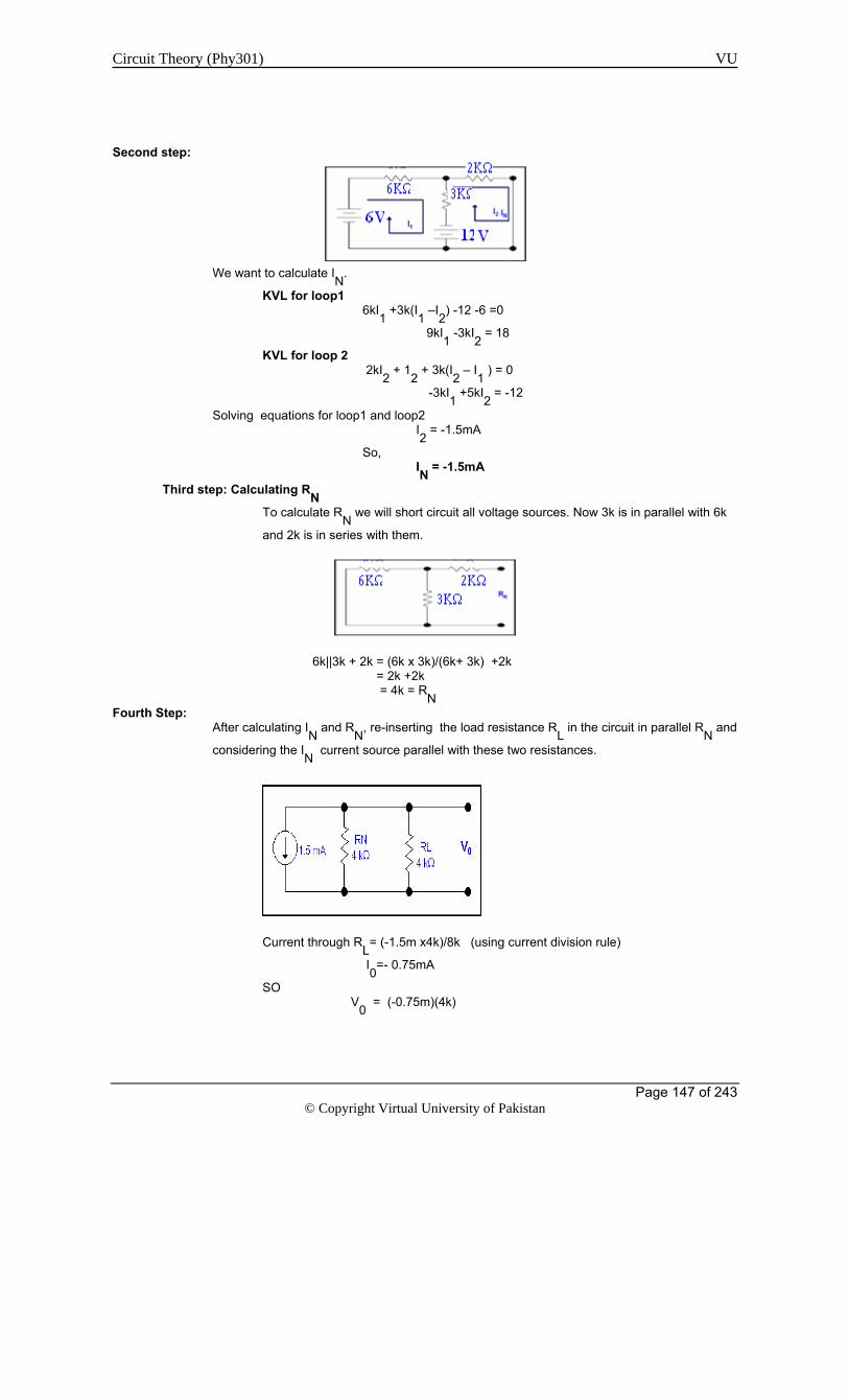
Circuit Theory (Phy301) VU
Page 147 of 243
© Copyright Virtual University of Pakistan
Second step:
We want to calculate I
N.
KVL for loop1 6kI
1 +3k(I
1 –I
2) -12 -6 =0
9kI1 -3kI
2 = 18
KVL for loop 2 2kI
2 + 1
2 + 3k(I
2 – I
1 ) = 0
-3kI1 +5kI
2 = -12
Solving equations for loop1 and loop2 I
2 = -1.5mA
So, IN = -1.5mA
Third step: Calculating RN To calculate R
N we will short circuit all voltage sources. Now 3k is in parallel with 6k
and 2k is in series with them.
6k||3k + 2k = (6k x 3k)/(6k+ 3k) +2k = 2k +2k = 4k = R
N Fourth Step:
After calculating IN
and RN
, re-inserting the load resistance RL in the circuit in parallel R
N and
considering the IN
current source parallel with these two resistances.
Current through R
L= (-1.5m x4k)/8k (using current division rule)
I0=- 0.75mA
SO V
0 = (-0.75m)(4k)

Circuit Theory (Phy301) VU
Page 148 of 243
© Copyright Virtual University of Pakistan
V0= - 3volts
Example: Calculate the voltage Vo by using Norton’s theorem .
Solution: We want to calculate V
0 by using Norton’s theorem.we will follow these steps .
First step: Replacing RL with a short circuit to find IN. Here RL is 4k resistor.
Second step:
I
sc =I
1 + I
2 For node 1 V
1/4k + (V
1 – 2)/3k + V
1/6k +4m=0
3V1 +4V
1 – 8 +2V
1 +48 =0
9V1+40=0
Or V1= - 4.44V
For node 2 V
2/2k + V
2/8k -4 =0
4V2 +V
2 – 32 =0
5kV2 = 32
V2 =32/5
V2= 6.4V
Now I
1 = V
2/8k

Circuit Theory (Phy301) VU
Page 149 of 243
© Copyright Virtual University of Pakistan
= 6.4/8k I1 = 0.8 mA
I2 = V
1/4k
= 4.44/4k = -1.11mA So, I
N = I
1+ I
2
IN
= (1.11 + 0.8)
IN = -0.31mA
Third step: Calculating RN To calculate R
N we will short circuit all voltage sources and open the current sources.
For RN
3k|| 6k = 2k 2k is in series with 4k = 2k + 4k = 6k 8k is in series with 2k = 8k + 2k =10k 10k ||6k = 10 x6/16 =60/16 R
N = 3.75k
Fourth Step: After calculating I
N and R
N, re-inserting the load resistance R
L in the circuit in parallel R
N and
considering the IN
current source parallel with these two resistances.
To calculate V0
I0 = 0.31m x 3.75k x 1/(4k+3.75k)
= 0.14mA V
0 = 4k x 0.14m
V0 = 0.56 Volts

Circuit Theory (Phy301) VU
Page 150 of 243
© Copyright Virtual University of Pakistan
LLEECCTTUURREE 2288
(Norton's Theorem with examples - Linearity Principle) Example: Find Norton equivalent circuit.
Solution: First step: Removing RLreplace open circuit with short circuit
by ohm’s Law we have IN=12/~0 → ∞A
Now we will insert the resistance R=~0 parallel to current source.
So we have the Norton’s equivalent circuit. Example: Calculate Norton’s current through the circuit.
Solution: Inject a 1A current source into the port and define Vx across 200Ω so that
For node 1 1=(V
1/100)+(V
1-V
x)/50
100=V1+2V
1-2V
x 3V1-2Vx=100 ----------------- (A)
For node 2 -0.1V
1=(V
x/200)+(V
x-V
1)/50
-20V1=V
x+4V
x-4V
1

Circuit Theory (Phy301) VU
Page 151 of 243
© Copyright Virtual University of Pakistan
5Vx+16V1=0 ----------------(B)
Solving simultaneously A and B we have 10Vx+32V1= 0 -10Vx+15V1= 500 47V1= 500 V1=10.64V Also Rth= Rn =V1/1A =10.64Ω Since no independent source is involved in the circuit, hence I
N=0
Example: Calculate the voltage Vo by using Norton’s theorem , do not use loop and node methods. Use
super postion method.
Solution: We want to calculate V
0 by using Norton’s theorem.we will follow these four steps .
First step: Replacing RL with a short circuit to find IN.
Here R
L is 6k resistor.
Second step: We cant use loop or node methods, so lets use super position method to calculate I
N
To apply super position method we will remove all circuits one by one i.e. after removing voltage source we will replace it with short circuit and current source with open circuit. Hint: Don’t remove all circuits simultaneously. Only current source is acting.
Due to short circuit all current will follow through the short circuit so IN1 = 2mA --------------(A)
Only voltage source is acting.
4k is in parallel with 2k resistor which in return in series with 2k resistor .So total resistance. R = (4k||2k) +2k = 8/6 k +2k

Circuit Theory (Phy301) VU
Page 152 of 243
© Copyright Virtual University of Pakistan
R = 3.33 k So I
N2 = 6/3.33k
IN2 = 1.80mA -------------- (B)
total I
N from both sources so from equation A and B we have
IN
= IN1
+ IN2
= 2mA + 1.80mA = 3.80mA
Third step: Calculating RN To calculate R
N we will short circuit all voltage sources and open circuit all current
sources.
4k is in parallel with 2k.The combined effect of these is in series with 2k. 4k||2k + 2k = 1.33 + 2k =3.33k =R
N Fourth Step:
After calculating IN
and RN
, re-inserting the load resistance RL in the circuit in parallel R
N and
considering the IN
current source parallel with these two resistances. So our Norton
equivalent circuit will be.
by current divider rule we have I
0 = ( 3.80m)(3.33) x 1/9.33k
= 1.356 mA By ohm’s Law we have V0 = 6k x 1.35 = 8.143 volts

Circuit Theory (Phy301) VU
Page 153 of 243
© Copyright Virtual University of Pakistan
Example: Calculate the current Io by using Norton’s theorem .
Solution: We want to calculate I
0 by using Norton’s theorem.we will follow these steps .
First step: Replacing RL with a short circuit to find IN. Here RL is 6k resistor.
Second step: Calculate current IN
From loop 2, we can write I2=2mA
For loop 1 4k(I1-IN)+2k(I1-I2)-6=0 4kI
1-4kI
N+2kI
1-2kI
2-6=0
6kI1-4kI
N-2kI
2=6
Putting the value of I2
6kI1-4kI
N-2k(2m) = 6
6kI1-4kI
N = 10
For Loop 3 4k(IN-I2)+4k(IN-I1)=0 4kI
N-4kI
2+4kI
N-4kI
1=0
-4kI1+8kI
N=8
Solving equations for loops 1 and 3 12kI1-8kIN=20
-12kI1+24kIN=24
16kIN=44
IN = 2.75 mA

Circuit Theory (Phy301) VU
Page 154 of 243
© Copyright Virtual University of Pakistan
Third step: Calculating RN To calculate R
N we will short circuit all voltage sources and open the current sources.
For R
N
2kII4k+4k =((2kx4k)/(2k+4k))+4k RN = 5.33kΩ Fourth Step:
After calculating IN
and RN
, re-inserting the load resistance RL in the circuit in parallel R
N and
considering the IN
current source parallel with these two resistances.
Io= (2.75m) (5.33k)x1/(6+5.33)k) Io =1.29mA \

Circuit Theory (Phy301) VU
Page 155 of 243
© Copyright Virtual University of Pakistan
Linearity Principle In this technique we assume the unknown quantity and analyze the circuit in reverse manner. Until we reach the source which is producing all voltages or currents and calculate its value. Now by comparing this value with the original value of the source we calculate the exact unknown quantity of the circuit. Example: Calculate Voby linearity principle.
Solution: We want to calculate V
oby linearity principle. Let us assume that V
o is 1 Volt.
Our assumption is Vo=1V Therefore, V2=1V Hence I2=1/2k=0.5mA Also, V4k=(0.5m)(4k)=2V Now, V1=V4k+V2= 2+1= 3V
Then, I1=3/3k=1ma
Also, Is=I2+I1=0.5m+1m=1.5mA
V2k=Is(2k)=2k(1.5m)=3V Vs=V2k+V1=3+3=6V When Vo is 1, source voltage is 6V, but original source voltage is 12 V, hence output voltage will be 2 Volts.

Circuit Theory (Phy301) VU
Page 156 of 243
© Copyright Virtual University of Pakistan
LLEECCTTUURREE 2299 (Basic semicoconductor concepts)
INTRINSIC SILICON:
A crystal of pure or intrinsic silicon has a regular lattice structure. Where the atoms are held at their fixed positions by bonds, called Covalent bonds, formed by four valence electrons associated with four each silicon atom.
At sufficiently low temperature these covalent bond are intact and not (very few) free electrons are available to conduct electric current.
Thermal ionization results in free electrons and holes in equal numbers and hence equal concentrations. These free electrons and holes move randomly through silicon crystal structure, and in this process some electrons may fill some of the holes. This process is called RECOMBINATION
It results in disappearance of free electrons and holes. The recombination rate is proportional to the number of free electrons and holes, which in turn is determined by ionization rate.
CONDUCTION BAND: In semiconductors and insulators, there is a band gap above the valence band, called a conduction band. In a semiconductor, the range of electron energy, higher than that of the valence band, sufficient to make the electrons free to move from atom to atom under the influence of an applied electric field and thus constitute an electric current.
Valence BAND: AT OO C the outermost electrons of an atom of a semiconductor material (such as silicon and germanium) are present in valance-orbits. Associated with these orbits is a band of energies that is termed as valence band of energy. BAND GAP: The difference of energy between valance band and conduction band is called band gap energy.
In the above fig upper line is denoted as conduction band while lower line is valance band. There are no electrons available in these energy bands. Drift The process whereby charged particles move under the influence of electric field.
In the above fig there are few electrons present in the near by valance band if we apply some electric field to such a material then these electrons due to applied electric field may drift hence we can observe some activity into electrical property of the material therefore some flow of current also observe and we say this is a conductor.
In the above fig all the energy levels are fully filled with electron if we apply any electric field to such a material then these electrons have no space to drift hence such material act as insulator. Insulators are such material which offers maximum resistance to the flow of electrons and their conductivity is very
low.

Circuit Theory (Phy301) VU
Page 157 of 243
© Copyright Virtual University of Pakistan
in the above fig almost all energy levels are full except two levels are kept empty if we apply electric field to such a material then these electrons have some space to drift therefore we will observe some flow of current through such a material so these material are called conductors. Conductors are such materials s which offers zero resistance to the flow of electrons and their conductivity is maximum. BAND GAP ENERGY: It is the energy required to excite an electron from its valence band to a conduction band and denoted as Eg. as show in the fig below
Diffusion The process of flow of particles from a region of high concentration to a region of low concentration. Diffusion Current The current that results from the diffusion of charged particles. Drift Velocity The average velocity of charged particles in the presence of an electric field. DOPED SEMICONDUCTORS
Doped semiconductors are the materials in which carrier of one kind (electrons or holes) predominate. Doped silicon in which the majority of charge carriers are negatively charged electrons is called n type. While silicon doped so that majority of charge carriers are positively charged holes is called p type. Doping of silicon to turn it into p type or n type is achieved by a small number of impurity atoms. For instance, introducing impurity atoms of a pentavalent element such as phosphorus results in n type
silicon. NO BIAS
THE DIFFUSION CURRENT I
D
Because the concentration of holes is high in the p region and low in the n region, holes diffuse across the junction from the p region to the n region.
Similarly, electrons diffuse the junction from n side to p side. These two current components add together to form the diffusion current I
D .Whose direction is from p
side to n side, as indicated in the figure.

Circuit Theory (Phy301) VU
Page 158 of 243
© Copyright Virtual University of Pakistan
THE DEPLETION REGION
The electrons that diffuse across the region quickly recombine with some of the majority holes present in the p region and thus disappear from the scene.
This results also in disappearance of some majority holes, causing some of the bound negative charge to be uncovered (i-e no longer neutralized by holes). Thus in the p material close to the junction that is depleted of free electrons.
This p region will contain uncovered bound negative charge, as indicated in the figure. From the above it follows that a carrier depletion region will exist on both sides of the junction. With n side of this region positively charged and p side negatively charged. This carrier depletion region
or simply, depletion region is also called the SPACE CHARGE REGION. THE P-N JUNCTION UNDER REVERSE BIAS CONDITION.
The pn junction is excited by a constant current source I in the reverse direction. To avoid breakdown, I
kept smaller than IS.
Note that the depletion layer widens and the barrier voltage increases by VR volts, which appears
between the terminals as reverse volt age. The current I will be carried by electrons flowing in the external circuit from the n material to p material
(that is, in direction opposite to that of I). This will cause electrons to leave the n material and holes to leave p material. Thus reverse current I
will result in an increase in the width of, and the charge stored in the depletion layer. Which will increase the voltage across depletion region?
THE P-N JUNCTION UNDER FORWARD BIAS CONDITION.
The pn junction is excited by a constant current source supplying a current I in forward direction. The
depletion layer narrows and barrier voltage decreases by V volts, which appears as an external voltage in the forward direction.
This current causes majority carriers to be supplied to both sides of the junction by the external circuit. Holes to the p material and electrons to the n material.
These majority carriers will neutralize some of the uncovered, causing less charge to be stored in the depletion region. Thus the depletion layer narrows and the depletion barrier voltage reduces.
This reduction in voltage cause more electrons to move from n side to p side and more holes to move from p side to n side. So that diffusion currents increases until equilibrium is achieved.

Circuit Theory (Phy301) VU
Page 159 of 243
© Copyright Virtual University of Pakistan
LLEECCTTUURREE 3300 (PN Junction Diode - Ideal Diode - Ideal Diode as a Rectifier) INTRODUCTION TO THE PN- JUNCTION DIODE. The schematic symbol for the pn-junction diode is shown in the fig.
A diode will conduct when it meets the condition that the voltage difference between the anode and the cathode exceeds the barrier voltage of approximately 0.3 volts for a germanium diode and 0.7 for a silicon diode. THE FORWARD BIASED PN-JUNCTION (DIODE) When positive terminal of a battery is connected to the anode or P-side and negative terminal to the cathode or to the N-side of a diode (PN-junction), the diode is said to be FORWARD-BIASED.
In the figures to follow it may be noted that the arrow points to the more negative potential in each case. In fig. a below the positive terminal of a battery through a resistor is connected the anode whereas the cathode is attached to the neutral terminal and now the condition of the forward biased is fulfilled. In fig. b below the negative terminal of a battery is connected to the cathode whereas the anode is attached through a resistor to the neutral terminal and now the condition of the forward biased is fulfilled where IF shows the forward conventional current.
In fig. c below the positive volts has been applied to the anode of the diode through a resistance and cathode terminal of the diode is connected to the neutral terminal through resistance which will fulfill the condition of forward biased. Where IF shows the forward conventional current.
In fig. d above the –ve volts has been applied to the cathode of the diode through a resistance and anode terminal of the diode is connected to the neutral terminal through resistance which will fulfill the condition of forward biased. Where IF shows the forward conventional current will be establish in the diode. THE REVERSE - BIASED PN-JUNCTION (DIODE)
When positive terminal of a battery is connected to the cathode or N-side and negative terminal to the anode or to the P-side of a diode (PN-junction), the diode is said to be REVERSED - BIASED.
A PN-junction diode is reverse biased when the n type material (cathode) is more positive than the p type material (anode). This causes the depletion region to widen and prevent current. A diode will not conduct when the arrow points to the more positive of the diode potentials.

Circuit Theory (Phy301) VU
Page 160 of 243
© Copyright Virtual University of Pakistan
In fig. a the negative of the battery is connected to the anode through a resistor and positive terminal of the battery is connected the cathode therefore no current will flow and we can say that diode is not existing and it will act as an open circuit. In fig. b the negative terminal of the battery is connected to the anode through a resistor and positive terminal of the battery is connected the cathode. The reverse – biased diode behaves opposite to the forward-biased diode. This means in case of a reverse-biased diode, majority carrier current does not flow and instead of that only minority carrier current can flow. Moreover, the depletion charge layer will expand or enlarged compared to the forward –biased diode where the depletion charge layer shrinks, so it will act as an open circuit.
In fig. c the negative voltage has been applied to the anode of the diode through a resistance and cathode terminal of the diode is connected to the neutral terminal through resistance. Which will fulfill the condition of reversed biased. In fig. d the positive voltage has been applied to the cathode of the diode through a resistance and anode terminal of the diode is connected to the neutral terminal through resistance. Which will fulfill the condition of reversed biased Here we can say that the reverse-biased PN-junction can’t support majority carrier current but it will allow the minority carrier current to flow across the junction. This minority carrier current is called as reverse current and is much smaller than the forward majority carrier current of the forward biased PN- junction.
The Ideal Diode The diode can be considered to be a one Way Street that is it conducts electricity well in one direction but hardly any in the opposite direction. An ideal diode has no resistance in the forward direction and infinite resistance in the reverse direction. An ideal diode is like a light switch in your home. When the switch is closed, the circuit is completed; and the light turns on. When the switch is open, there is no current and the light is off. However, the diode has an additional property; it is unidirectional, i.e. current flows in only one direction (anode to cathode internally).When a forward voltage is applied, the diode conducts; and when a reverse voltage is applied, there is no conduction. A mechanical analogy is a rat chat, which allows motion in one direction only.
The ideal diode may be considered the most fundamental non linear circuit element. It is a two terminal device and the i-v characteristic is shown

Circuit Theory (Phy301) VU
Page 161 of 243
© Copyright Virtual University of Pakistan
Fig a is diode circuit symbol, fig b is i-v characteristic fig c is equivalent circuit in the reverse direction and fig d is the equivalent circuit in the forward direction. In fig b the terminal characteristic of the ideal diode can be interpreted as. If a negative voltage is applied to the diode, no current flows and the diode behaves as an open circuit as shown in the fig c. Diodes operated in this mode are said to be reverse –biased. An ideal diode has zero current when operated in the reverse direction and is said to be cut off. On the other hand, if a positive voltage is applied to the ideal diode, zero voltage drop appears across the diode .In other words ideal diode behaves as a short circuit in the forward direction as show in the fig d , it passes any current with zero voltage drop. A forward –conducting diode is said to be turned on.
The Ideal Diode as a Rectifier Rectification is generally defined as the process of converting an alternating current to a unidirectional current. A rectifier device conducts current substantially in one direction only. An ideal rectifier diode would be an open circuit in one direction and short circuit in the other direction. It also would not dissipate power during the rectification process.
The rectifier circuit shown in the fig a . This circuit consists of series connection of a diode D and a resistor R. Let the input voltage be sinusoid as shown in fig b and assume the diode to be ideal. During the positive half cycle of the input sinusoid ,the positive vI will cause current to flow through the diode in its forward direction. It follows that the diode voltage VD will be very small i:e ideally zero. Thus the circuit will have the equivalent show in the fig (c) and the output voltage VO will be equal to the input voltage vI. On the other hand ,during the negative half cycle of vI the diode will not conduct .Thus the circuit will have the equivalent show in the fig (d), and VO will be zero .Thus, the output voltage will have the waveform shown in fig (e).Note that when VI alternates in polarity and has a zero average value , VO is unidirectional and has a finite average value or a dc component. Thus the circuit of fig (a) rectifier the signal and hence is called a rectifier.
Example: For the circuit draw transfer characteristic v0
VS vI
Solution:

Circuit Theory (Phy301) VU
Page 162 of 243
© Copyright Virtual University of Pakistan
LECTURE 31 (Terminal characteristics of the Junction diodes - Forward bias region) Example Fig shows a circuit for charging a 12 volts battery. If vs is a sinusoid with 24 volts peak amplitude, find the fraction of each cycle during which the diode conducts also find the peak value of the diode current and the maximum reverse biases voltage that appears across the diode.
Solution : The diode conducts when vs exceeds 12 volts as shown in the previous fig. The conduction angle is 2θ, where θ is given by 24cosθ =12 cosθ = 1/2
θ = cos-1
(1/2)
Thus θ= 60o
and the conduction angle is 120o
or one third of the cycle. The peak value of the diode current is given by
Id = 24 – 12/100
= 0.12 A The maximum reverse voltage across the diode occurs when vs is at its negative peak and is equal to 24 +12 =36 volts Example: Assuming the diodes to be ideal .Find the value of I and V in the circuit shown in figure below.
Solution : We are using ideal diode here. In fig (a) positive 5 Volt battery is connected to the anode of the diode through a resistance of 2.5 k ohm. The cathode terminal of the diode is connected with the neutral terminal. The diode is in forward biased condition. From the fig we see that all components are in series so the same current will flow. so by Ohm’s Law we have I = 5/2.5 I = 2mA ` diode acting as short circuit so, V=0 volts In fig (b) the circuit is same only the diode has reversed. 5 Volt battery is connected to the cathode of the diode through a resistance of 2.5 k ohm. The anode terminal of the diode is connected with the neutral terminal. Now the diode is in reversed biased condition so, it will act as an open circuit therefore no current will flow. I = 0mA whole voltage of 5 volts will appear at positive terminal. V= 5volts

Circuit Theory (Phy301) VU
Page 163 of 243
© Copyright Virtual University of Pakistan
In fig (c) negative 5 Volt battery has been connected to the anode of the diode through a resistance of 2.5 k ohm. The cathode terminal of the diode is connected with the neutral terminal. The diode is in reversed biased condition and it will act as an open circuit therefore current will flow. I = 0mA whole voltage of 5 volts will appear V= - 5volts In fig (d) the circuit is same only the diode has reversed. negative 5 Volt battery has been connected to the cathode of the diode through a resistance of 2.5 k ohm. The anode terminal of the diode is connected with the neutral terminal. Now the diode is in forward biased condition so, it will act as an short circuit therefore current will flow. so by Ohm’s Law we have I = 5/2.5 I = 2mA diode acting as short circuit so, V=0 volts Example Assuming the diodes to be ideal, find the values of I and V
0 in the circuits.
Solution :
For the circuit in the fig (a) we shall assume that both diodes are conducting. It follows that VB = 0 and V0 = 0. The current through D2 can now be determined from
ID2 = (10 – 0)/10 = 1mA
Writing node equation at B,
I + 1 = 0 – (-10)/5 Results in I =1mA. Thus D
1 is conducting as originally assumed, and the final result is
I = 1mA and V=0 volts For the circuit in fig (b), if we assume that both diodes are conducting , then V
B =0
and V0
= 0 . The current in D2 is obtained
from I
D2 = (10 -0)/5 = 2mA

Circuit Theory (Phy301) VU
Page 164 of 243
© Copyright Virtual University of Pakistan
e node euation at B is
I + 2 m = 0 – (-10)/10k Which yields I = -1mA. Since this is not possible , our assumption is not correct. we start again, assuming that D
1 is off and D
2 is on.
The current ID2
is given by
ID2
= 10 – (-10)/15
= 1.33mA and the voltage at node B is V
B = -10 + 10 x 1.33 = 3.3 volts
Thus D1 is reversed biased as assumed, and the final result is I =0 and V
0 =3.3 volts
TERMINAL CHARACTERISTICS OF THE JUNCTION DIODS
As indicated the characteristic curve consist of thee distinct regions: (1) The forward bias region, determined by v >0 (2) The reverse bias region determined by v<0
(3) The breakdown region determined by v< -VZK
These three regions of operations described in the following. THE FORWARD BIAS REGION:
The forward bias or simply forward region is entered when the terminal voltage v is positive. In the forward region the i-v relationship is closely approximated as
i = Is(ev/nV
T – 1)
In this equation Is is a constant for a given diode at a given temperature and it is directly proportional to
the area of the diode. The Voltage V
T is a constant and given as
VT = kT/q
where k = Boltzmann,s constant
= 1.38 x10⁻²³
jouls/kelvin T= absolute temperature in kelvin q =magnitude of the electronic charge
=1.60 x10⁻¹⁹
coulombs
At room temperature (20 o
C) the value of VT
is 25.2mV.
In the diode equation the constant n has a value between I and 2 depending on the material and physical structure of the diode.

Circuit Theory (Phy301) VU
Page 165 of 243
© Copyright Virtual University of Pakistan
For appreciable current I in the forward direction , i>> Is. The diode equation can be modified as
i = Isev/nVT
This expression can be given alternatively in algorithmic form
v = nVTln(i/Is)
Let us consider the forward i-v relationship and evaluate the current I1 corresponding to the diode
voltage V1:
I1 = IseV1/nVT
Similarly, if the voltage V2 the diode current I
2 will be
I2 = Is eV2/nVT
These two equations can be combined to produce
I2/I1 = e(V2 – V1)/nVT
Which can be rewritten as V2 – V1 = nVTln(I2/I1)
EXAMPLE: A silicon diode said to be 1mA device displays a forward voltage of 0.7 V at a current of 1mA. Evaluate the junction scaling constant I
s in the event that n is either 1 or 2 .What scaling constant would apply for a 1A
diode of the same manufacture that conducts 1A at 0.7V. SOLUTION:
Since
i =Isev/nVT
Then
Is = ie
-v/nVT
for 1mA diode:
if n=1 : Is = 10
-3 e
-700/25
Is = 6.9 x10¹⁶
A
If n =2 : Is =10
-3 e
-700/50
Is = 8.3 x10⁻¹⁰
A
The diode conducting 1A at 0.7V corresponds to 1000mA in parallel with a total junction area 1000 times greater. Thus Is is also 1000 times greater.

Circuit Theory (Phy301) VU
Page 166 of 243
© Copyright Virtual University of Pakistan
LECTURE 32 (Reverse bias region - Break down region - Analysis of diode circuit) Example: Consider a silicon diode with n =1.5. Find the change in voltage if the current changes from 0.1mA to 10mA. Solution:
i = Is ev/nVT
I1 =Is e
v1/nVT
I2
= Is ev2/nVT
I1/I
2 = e
(v1 –v2)nVT
v 1–v2 = nV
Tln(I
1/I
2)
here,
VT= 25 mV
= 1.5 x25 ln( 10/0.1) so change in the voltage will be v1 –v2 = 172.7mV Example: A silicon junction diode with n =1 has v = 0.7 volts at i =1mA . Find the voltage drop at i =0.1mA and i = 10mA. Solution: v
2 –v
1 = nV
Tln(i
2/i1)
v1 = 0.7V
i1 = 1mA
and n =1 thus v
2 = 0.7 +V
Tln(i
2)
for i
2 = 0.1mA
VT= 25 mV=0.025 volts
v2 = 0.7 + 0.025ln(0.1)
v2= 0.64 volts
For i
2 = 10mA
v2 = 0.7 + 0.025ln(10)
v2 = 0.76volts
Example: The circuit in the fig. utilize three identical diodes having n=1 and Is = 10
-14 A .Find the value of the
current I to obtain an output voltage V0 = 2V, if a current of 1mA is drawn away, what is the change
in output voltage.
Solution: For V
0 =2V, so the voltage drop across each diode is 2/3V.
Thus I must be
I = Is ev/nVT
VT= 25 mV=0.025 volts

Circuit Theory (Phy301) VU
Page 167 of 243
© Copyright Virtual University of Pakistan
= 10-14
e2/3x0.025
=3.8mA If a current of 1mA is drawn away from the terminals by means of a load, the current though the diodes reduces to 3.8 – 1 = 2.8 Thus the voltage across each diode changes by ∆V = v
2 –v
1 = nV
Tln(i
2/i1)
∆V =nV
T ln(2.8/3.8)
= -7.63mV The total decrease in V
0
V0 = 3 x 7.63
= 22.9Mv Example: A particular diode conducts 1A at a junction voltage of 0.65 volts and 2A at a junction voltage 0.67 volts. What are its values of n and Is , what current will follow if its junction voltage is 0.7volts? Solution:
I = Is eVD /nVT -------------- (A)
VD is a diode voltage.
VT= 25 mV=0.025 volts
1= Is e
0.65/n(0.025) -------------- (B)
2 = Is e0.67/n(0.025) ------------- (C)
Taking natural log of (B) and (C) and subtracting we have
ln (1) = ln( Is l e0.65/n(0.025)
)------ (B)
ln(2) = ln (Is e0.67/n(0.025)
)------ (C) Subtracting (B) and (C) we have - ln 2 = - 0.02/n(0.025)
n = 0.02/0.025ln2 n = 1.154 put the value of n in equation B we have
Is = e -0.65/1.154(0.025)
= 1.64 x 10⁻¹⁰
so from equation A we have
ID
= 1.64 x10⁻¹⁰
e0.7/1.154(0.025)
ID
= 1.64 x10-10
X 3.4 x 1010
ID = 5.66A
THE REVERSE BIAS REGION:
The reverse bias region of operation is entered when the diode voltage is made negative. The previous equation indicates that if v is negative and a few times larger then VT in magnitude the exponential term
becomes negligibly small as compared to unity and diode current becomes i = -I
s that is, the current in the reverse direction is constant and equal to Is. This constancy is the reason behind the term saturation current . A good part of the reverse current is due to the leakage effect.
The leakage currents are proportional to the junction area, just as Is. Its dependence on temperature is however, different from that of Is.
THE BREAKDOWN REGION: The break down region is entered when the magnitude of the reverse voltage exceeds a threshold value
specific to a particular diode and is called the BREAKDOWN VOLTAGE.

Circuit Theory (Phy301) VU
Page 168 of 243
© Copyright Virtual University of Pakistan
It is the voltage at the knee of i-v curve and is denoted by VZK.
In the break down region reverse current increases rapidly , while the associated change in voltage is very small this fact is used in voltage regulation.
ANALYSIS OF DIODE CIRCUITS:
Consider the circuit shown in the fig. We wish to analyze this circuit to determine the diode current I
D
and voltage VD
.
The diode is obviously biased in forward direction. Assuming that V
DD is greater than 0.5V or so, the diode current will be much greater than Is and we
can represent i-v characteristics by the exponential relationship resulting in
ID
= Is eVD/nVT
(1)
The other that governs circuit operations is obtained by writing a KVL equation resulting in I
D = (V
DD – V
D) / R …(2)
if we put ID=0 in equation 2 we will get VDD = VD
if we put VD = 0
ID = VDD / R
We draw current along Y-axis and voltage across X-axis GRAPHICAL ANALYSIS:
Graphical analysis is performed by plotting the relationships of equations (1) and (2) on the i-v plane .The solution can then be obtained as the point of intersection of the two graphs.
A sketch of the graphical construction is shown in the fig. The curve represents the exponential diode
equation and the straight line represents the equation (2). Such a straight line is known as load line . The load line intersects the diode curve at point Q, which represents the operating point of the circuit. It co-ordinates gives values of I
D and V
D
ITERATIVE ANALYSIS: Equations (1) and (2) can be solved using a simple iterative procedure, as illustrated in the following
example

Circuit Theory (Phy301) VU
Page 169 of 243
© Copyright Virtual University of Pakistan
EXAMPLE: Determine the current ID
and the diode voltage VD
for the circuit in the fig. with VDD
= 5V and
R =1k. Assume that the diode has a current of 1mA at a voltage of 0.7V and its voltage drop changes by 0.1V for every decade change in current.
SOLUTION: To begin the iteration, we assume that V
D = 0.7V and the equation (2) determines the current
ID
= VDD
– VD
/R
= 5 – 0.7/1 = 4.3mA Now from our previous knowledge V2 – V1 = nVTln(I2/I1)
log 10 x = (ln x)/ (ln 10) where ln10 =2.3
so 2.3 log 10 x = ln x
now the equation of log to the base 10 form will be as V2 – V1 =2.3nV
TlogI
2/I
1 For our case, 2.3 nV
T = 0.1volts
V2 = V1 + 0.1logI2/I
1 Substituting V1 =0.7V, I
1 =1mA and I
2 =4.3mA
V2 = 0.763V
Thus the results for the first iteration are ID =4.3mA and VD =0.763 V
The second iteration proceeds in the similar manner
ID
= VDD
– VD
/ R
Here VD
= 0.763 V
ID
= 5 – 0.763/1
= 4.237mA V2 = 0.763 + 0.1 log(4.237/4.3) = 0.762 V Thus the second iteration yields ID = 4.23mA and VD = 0.762V
Since these values are not much very different from the values obtains after the first iteration, no further iterations are necessary and the Solution is ID = 4.23mA and VD = 0.762V

Circuit Theory (Phy301) VU
Page 170 of 243
© Copyright Virtual University of Pakistan
LLEECCTTUURREE 3333 (DC or Static Resistance-The constant voltage drop model - AC or Dynamic Resistance) DC OR STATIC RESISTANCE:
When diode is subjected to a dc voltage its operating point on the characteristic curve does not change with time. Hence the resistance of the diode can be found easily
rD =vD/iD
It may also be seen on the curve that the resistance in the reverse bias is quite high.
Example: Determine the resistance level for the diode having characteristics as shown in the graph below at (1)ID =1mA
(2)ID=20mA
(3)VD= -10V
SOLUTION:
(1) From the curve
For ID =1mA ,VD=0.5volts
RD = 0.5/1m
RD = 500 ohms
(2) For ID =20mA , VD = 0.8volts RD = 0.8/20m
RD = 40ohms

Circuit Theory (Phy301) VU
Page 171 of 243
© Copyright Virtual University of Pakistan
(3) For VD = -10V, ID = -1microA
RD = 10/10-6
RD = 10Mohms
THE CONSTANT VOLTAGE DROP MODEL: We use a vertical straight line to approximate the fast rising part of the exponential curve, as shown in
the fig.
Ideal Model: We have seen that the diode behaves essentially as a switch: on when forward biased, off when reverse biased. The ideal diode characteristic is shown in Figure B. Corresponding to this is the ideal diode model, Figure C.
Figure B: Ideal diode characteristic.
Figure C: Ideal diode model. When the diode is reverse biased, we replace it with an open switch, and when the diode is forward biased, we use a closed switch.

Circuit Theory (Phy301) VU
Page 172 of 243
© Copyright Virtual University of Pakistan
PRACTICAL MODEL:
In practice we find that there is a voltage drop of about 0.7 V across the diode (silicon; germanium is 0.3 V) when it is forward biased, and so it is often useful to include this voltage drop in circuit analysis. Accordingly, the practical model is the ideal model with the addition of a voltage source in the forward bias model. Figure D shows the practical model characteristic. The practical model is shown in Figure E.
Figure D: Practical diode characteristic.
Figure E: Practical diode model.
The resulting model simply says that a forward conducting diode exhibits a constant voltage drop V
D.
The value of VD
is usually taken to be as 0.7 volts in case of silicon diode. The constant voltage drop
model can be represented by the equivalent model shown in the fig.
THE EFFECT OF THE FORWARD VOLTAGE DROP ON CIRCUIT ANALYSIS To illustrate this effect consider this circuit,

Circuit Theory (Phy301) VU
Page 173 of 243
© Copyright Virtual University of Pakistan
According to the KVL, the sum of the component voltages in the circuit must be equal to the applied voltage .By formula Vs = V
F + V
R
Vs = voltage of source
VF
= forward voltage across the diode
VR
= voltage drop across I ohm resistance
if we consider diode is a silicon so, VF
=0.7 volts and arrange this equation for VR
then
VR
= Vs – 0.7V
According to ohms law IT = VR / R
Putting the value of VR
from this equation
IT
= Vs – 0.7/R1
Putting the value of R1 we have = 5 – 0.7/1 = 4.3A If we consider this diode to be ideal than no voltage drop will occur across it and we will get Vs = V
R
VF
= 0
IT
= 5mA
Example: Find voltage across R1. Consider silicon diode so that 0.7 V drop is assumed across it.
Solution:
By KVL V
s=V
R+V
f V
R=V
s-0.7
VR
= 6 - 0.7
= 5.3 volts≈5 Volts. THE CONSTANT VOLTAGE DROP MODEL:
(1) Diode current will remain at zero until the knee voltage is reached. (2) Once the applied voltage reaches the value of V
k , the diode turns on and the forward conduction
occurs. (3) As long as the diode conducting, the value of V
F is approximately equal to v
K. In other words the value
of VF
is assumed to be 0.7volts regardless of the value of IF
.
AC OR DYNAMIC RESISTANCE:
rD = ∆vD/ ∆iD ∆ shows a finite change in the quantity. The resistance in the vertical rise region is small, where as ac resistance is much larger at low current levels.

Circuit Theory (Phy301) VU
Page 174 of 243
© Copyright Virtual University of Pakistan
LECTURE 34 (Small Signal Model and its applications) EXAMPLE: Find the AC resistance for the curve shown at (1) ID = 2mA
(2) ID = 25mA
SOLUTION: (1) Choosing a swing of pulse minus 2mA For ID = 4mA, VD =.76V And ID = 0mA , VD =0.65V ∆ ID =4 – 0 = 4mA ∆ VD =0.76 -0.65 =.11V
rD = 0.11/4m = 27.5 ohms
(2) Choose a swing of pulse minus 5mA ∆I = 30 – 20 = 10mA
∆VD = 0.8 -0.78 = 0.02V rD = 0.02/10 = 10 ohms

Circuit Theory (Phy301) VU
Page 175 of 243
© Copyright Virtual University of Pakistan
SMALL SIGNAL MODEL In some applications circuit is supplied to a bias to operate in the forward region and also a small ac signal is super imposed on dc quantity consider the circuit shown
When there is no ac, diode voltage is VD so that
ID
=IS
eVD / nVT
and when signal Vd (t) is applied, then instantaneous voltage Vd(t) is v
D(t) = V
D +vd(t)
so that instantaneous diode current will be
iD
(t) =Is evD/nVT
Substituting for vD
iD
(t) =ISe(VD+ vd)/nVT
Or = Ise VD /nVT
. e vd /nVT
Or iD
(t) = I D
e vd / nVT
----------------- (A)
If the amplitude of the signal is sufficiently smaller than 1 , so that Vd/nVT
<<1 expanding the previous
equation in the form of a taylor series i.e
ex= 1+ x / 1!+ x
2/ 2! ………
Above expression is a taylor series expansion of exponential function ex
in the equation (A) x = Vd /nVT ,so we solve the equation (A) upto two terms by taylor series
e vd /nVT
= ( 1 + vd/nVT
)
put this value in equation (A) we have i
D(t) = I
D ( 1 + vd /nV
T)
= ID
+ ID
/nVT
vd --------------- (B)
Or we may write
ID
/nVT
vd = id put in equation (B) we have
iD
=ID
+ id
From previous equation we may see that the quantity ID
/nVT
has the dimensions of conductance given
in mho’s and is called diode small signal conductance .The inverse of it is called small signal resistance or incremental resistance given by r
d= nV
T/I
D
rd α 1/I
D
nV
T are constants and are provided by the manufacturer.
APPLICATION: Consider the circuit as shown, for analysis purposes, we can split the circuit into two parts that is ac and dc

Circuit Theory (Phy301) VU
Page 176 of 243
© Copyright Virtual University of Pakistan
DC source having the value of VDD
we replace the ac and replace diode with constant drop model
For dc analysis the Circuit will be
in case of DC we consider only DC current ID
is flowing and no effect of the ideal diode because this
ideal diode is forward biasing and it results in short circuit therefore From KVL V
DD –I
DR – V
Do – I
D r
d = 0
VDD
= ID
R+ VDo
+ ID
rd ---------------- (A)
in case of DC only DC current ID
is flowing the
For ac analysis we will remove DC sources which are the part of the original circuit and also remove the DC source which appear in the previous effective circuit and we also remove the ideal circuit so our circuit will be as
For ac analysis v
s = i
d (R + r
d) ------------- (B)
by combining (A) and (B) Overall analysis is V
DD + v
s =I
DR + V
Do + I
D r
d + i
d (R + r
d)
= ID
(R + rd) + i
d (R + r
d) +V
Do
VDD
+ vs = (R + r
d)( I
D + i
d) + V
D0 ------------ (C)
But ID + id = iD
therefore V
DD+ v
s = (R + r
d)( I
D + i
d) + V
D0
separating the dc and signal quantities on both sides of equation (C) V
DD = I
DR + V
D0 which is represented by the circuit in the figure below
and for the signal v
s = i
d (R + r
d)
which is represented by the circuit in the figure below

Circuit Theory (Phy301) VU
Page 177 of 243
© Copyright Virtual University of Pakistan
However, if we carefully see the ac equation circuit, it is nothing more than a voltage divider. Hence the diode signal voltage will be Vd = Vs rd/(rd +R) EXAMPLE: Find the value of the diode small signal resistance r
d at bias current of 0.1,1 and 10mA.
Assume n =1 SOLUTION: r
d = n V
T/ I
where VT =25m Volt
= 1 x25m / I for I = 0.1mA, r
d = 250ohms
I = 1mA, rd = 25ohms
I = 10mA, rd = 2.5ohms
EXAMPLE: For the diode that conducts 1mA at a forward voltage drop of 0.7 V and whose n =1. Find the equation of the straight line tangent at I
D = 1mA.
SOLUTION:
Slope = 1/ r
d
= I /nVT
= 1mA/1x25mV =1/25ohms Now on VD axis it will be
= 0.7 – 1m (25) = 0.7 - 0.025 = 0.675 V So by the equation of straight line y - y1= m (x-x1)
here m is a slope = 1/25ohms i
D = 1/25 (V
D -0.675)
VD
– 0.675 – iD
(25) =0
Which is the required equation of straight line.
EXAMPLE: Consider a diode with n = 2 biased at 1mA. Find the change in current as a result of changing the voltage by (a) – 20 mV (b) – 10 mV (c) – 5mV
(d) +5mV (e) +10mV (f) +20mV In each case do calculations (1) using small signal model (2) using the exponential model.

Circuit Theory (Phy301) VU
Page 178 of 243
© Copyright Virtual University of Pakistan
SOLUTION: For small signal model we have ∆v = r
d ∆i
∆i = ∆v / rd
But rd = n VT / I
=2 x 25m/1m = 50ohms ∆i = ∆v / 50 Now from exponential model
i = Is e v / nVT
Also we know that
ID
+ ∆i = ID
e ∆v/nVT
ID
+ ∆i = ID
e ∆v/nVT
∆i = ID
(e ∆v/nVT
- 1)
but I
D = 1mA thus
∆i = (e∆v/nVT
-1)
(a) For V = – 20 mV (1) ∆i = -20/50 = - 0.4mA
(2) ∆i = e-20m/50m
-1
= 0.33mA (d) ∆v = 5mV (1) ∆i = 5/5o = 0.10mA
(2) ∆i = e5/50
– 1 =0.11mA (f) ∆v = 20mV (1) ∆i =20/50 = .40mA (2) ∆i = e20/50 – 1 = 0.49mA

Circuit Theory (Phy301) VU
Page 179 of 243
© Copyright Virtual University of Pakistan
EXAMPLE: Design the circuit in the fig. so that V0 = 3V when I
L =0,and V
0 changes by 40mV per 1mA of
load current .Find the value of R .(assume four diodes are identical) relative to a diode with 0.7 drop at I mA current. Assume n =1
SOLUTION: V
0 = 3V, when I
L =0, therefore each diode should exhibit a drop of 0.75V. If I
L =1mA, then V
o
changes by 40mV and a change due to each diode is 10mV. Hence rd = 10mV/1mA =10 Ohms but rd = nV
T/ID
10 = 1 x 25m/ID
ID
= 2.5mA
Hence 15 – 3 – ID
RD
= 0
R = (15 – 3)/ID
= (15 – 3)/2.5m = 4.8k Ohms.

Circuit Theory (Phy301) VU
Page 180 of 243
© Copyright Virtual University of Pakistan
LECTURE 35 (Transformers - Secondary voltage and current - Transformer Input/Output phase relationship)
TRANSFORMERS:
Transformers are not semiconductor devices; however, they play an integral role in the operations of most of power supplies.
The basic schematic symbol for the transformer is as shown in figure,
The transformer basically consists of two inductors, which are in close proximity to each other. However, they are not physically connected. The device consists of two windings called the primary and secondary windings. The input to the transformer is applied to the primary. The output is taken from the secondary of the device. An alternating voltage is applied to the primary which induces an alternating voltage in the secondary. However, keep in mind that primary and secondary windings are physically isolated. A transformer can be designed in three modes.
1. STEP UP TRANSFORMER: The step up transformer provides a secondary voltage which is greater in amplitude as compared to primary.
For example, a step up transformer may provide a 240 Vac out put against 120 Vac at the in put. A step up transformer is shown
2. STEP DOWN TRANSFORMER:
The step down transformer provides a secondary voltage which is less than the primary voltage. For example, a transformer shown in the figure provides 30Vac at the out put against 120Vac input, as shown

Circuit Theory (Phy301) VU
Page 181 of 243
© Copyright Virtual University of Pakistan
3.ISOLATION TRANSFORMER: An isolation transformer provides an out put voltage that is equal to the input voltage.
These are used to electrically isolate power supplies from the power lines.
TURN RATIO;
• The turn ratio of a transformer is the ratio of number of turns in the primary to the number of turns in the secondary.
• For example, the step down transformer shown has a turn ratio of 4:1, which means there are four turns in the primary against each turn in the secondary.
•
The turn ratio of the transformer is equal to the voltage ratio of the two components, so that
Where
N2=Number of turns in the secondary winding. N1= Number of turns in the primary winding. V2=Voltage in the secondary. V1=Voltage to the primary.
CALCULATING SECONDARY VOLTAGE When turn ratio and the primary voltage is known, the secondary voltage can be found as V
2 = (N
2/N
1)V
1 For example the step down transformer in the previous fig. has 120 Vac input. The secondary voltage can be found as V
2 = (N
2/N
1) V
1 = 1/4(120Vac) V
2= 30Vac
CALCULATING SECONDARY CURRENT: Ideally, transformers are 100 percent efficient. This means that the ideal transformer can transfer 100 percent of its input power to the secondary. So that by formula we may write P2 = P1 Since power is equal to the product of voltage and current
V2I2 =V
1I1
and I
1/I
2 =V
2/V
1 The current ratio is inverse to the voltage ratio. This means that
(1) For step down transformer, I2>I
1 (2) For step up transformer, I
2<I
1

Circuit Theory (Phy301) VU
Page 182 of 243
© Copyright Virtual University of Pakistan
In other words, current varies opposite to the variation in voltage. If voltage increases, current decreases and vice versa. Since the Voltage ratio of a transformer is equal to the turn ratio therefore, the previous equation can be written as
I1/I
2 =N
2/N
1 I
2 = (N
1/N
2)I
1 EXAMPLE: The fuse in the figure is used to limit the current in the primary of the transformer. Assuming that the fuse limits the value of I1 to 1A, what is the limit on the value of the secondary current.
SOLUTION:
The maximum secondary current is found using the limit on I1 and the turn’s ratio as follows:
I2 =N1/N2 I1 = (1/4)1A I2 = 250mA
If the secondary current tries to exceed the 250mA limit, the primary current will exceed its limit and blow off the fuse. TRANSFORMER INPUT/OUTPUT PHASE RELATIONSHIP:
In the schematic symbol, there are two dots : one on the top side of the primary and the other on top of secondary. In this case we will be working with a transformer which does not produce any phase difference between the input and out put.
In the schematic symbol, there are two dots : one on the top side of the primary and one on the bottom side of the secondary, in this case
We are working with a transformer whose output voltage is 180o out of phase with its input voltage as
shown in fig.

Circuit Theory (Phy301) VU
Page 183 of 243
© Copyright Virtual University of Pakistan
HALF WAVE RECTIFIERS:
The half wave rectifier is made up of a diode and a resistor as shown in the fig. The half wave rectifier is used to eliminate either positive or negative part of the input.
Negative Half Wave Rectifiers:
Fig. shows a half wave rectifier with diode direction is reversed. In this circuit the diode will conduct on the negative half cycle of the input, and VL = V2.
The diode will be reversed biases for the positive half cycle of the input and VD = V2.
As a result positive half cycle of the input is eliminating. The operating principle of the negative half wave rectifier is same as the positive half wave rectifiers. The only difference is the polarity of the output will be reversed.
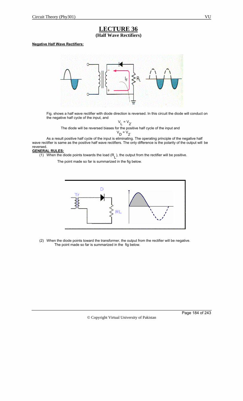
Circuit Theory (Phy301) VU
Page 184 of 243
© Copyright Virtual University of Pakistan
LECTURE 36 (Half Wave Rectifiers) Negative Half Wave Rectifiers:
Fig. shows a half wave rectifier with diode direction is reversed. In this circuit the diode will conduct on the negative half cycle of the input, and VL = V2.
The diode will be reversed biases for the positive half cycle of the input and VD = V2.
As a result positive half cycle of the input is eliminating. The operating principle of the negative half wave rectifier is same as the positive half wave rectifiers. The only difference is the polarity of the output will be reversed. GENERAL RULES:
(1) When the diode points towards the load (RL), the output from the rectifier will be positive.
The point made so far is summarized in the fig below.
(2) When the diode points toward the transformer, the output from the rectifier will be negative. The point made so far is summarized in the fig below.

Circuit Theory (Phy301) VU
Page 185 of 243
© Copyright Virtual University of Pakistan
CALCULATING LOAD VOLTAGE AND CURRENT VALUES. The load voltage in half wave rectifier can be found as VL(pk) = V2(pk) – VF
V2(pk) is the secondary voltage of the transformer, found as
V2(pk) = (N2/N1) V1 where N2/N1 =(The turn ratio of transformer secondary turns to primary turn) V
1(pk) = (The peak transformer primary voltage)
Above equation assumes that the transformer is given as a peak value. More often than not, source voltages are given as rms values. When this is the case, the source voltage is converted into peak value as follows: Vpk = Vrms/0.707
EXAMPLE: Determine the peak load voltage for the circuit shown in the fig.
IO
N SOLUTION: First, the ac input to the transformer is converted to a peak value, as follows V1(pk) = V1rms/0.707 = 120/0.707 = 169.7Vpk
Now, the voltage values in the secondary circuit are found as V2(pk) = N2/N1(V1pk)
= 1/5(169.7) V2(pk = 33.94Vpk
And VLpk = V2(pk) – VF diode is a silicon diode
= 33.94 – 0.7 VLpk = 33.24Vpk

Circuit Theory (Phy301) VU
Page 186 of 243
© Copyright Virtual University of Pakistan
EXAMPLE: Determine the peak load voltage for the circuit shown in the fig.
SOLUTION: The transformer is shown to have a 25V
ac rating .This value of V2 is converted into peak form as
V2(pk)
= V2rms
/0.707
= 25Vrms/0.707
V2(pk)
= 35.36Vpk
Now the value of Vpk is found as VL(pk) = V2(pk) – 0.7
= 35.36 – 0.7 VL(pk) = 34.66Vpk
CALCULATING LOAD CURRENT: Once the peak voltage is determined, the peak load current is found as IL(pk) = VL(pk)/RL
EXAMPLE: What is the peak load current for the circuit shown in fig.
SOLUTION: The input voltage is given an rms value. This value is converted to a peak value as follows: V
1(pk) = V
1(rms)/0.707
= 200Vac
/0.707
V1(pk) = 282.9 Vpk
Now, the load voltage and current are found, after fining peak voltage, as V
2(pk) = N2/N1 V1(pk)
= (1/5)(282.9 Vpk
)
V2(pk) = 56.6Vpk
Finally, the load voltage and current and current values are found as: V
L(pk) = V
2(pk) – V
F
= 56.6 – 0.7 VL(pk)= 55.9Vpk

Circuit Theory (Phy301) VU
Page 187 of 243
© Copyright Virtual University of Pakistan
and the current will be I
L(pk) = V
L(PK)/R
L
= 55.9 Vpk
/10k
IL(pk) = 5.59mApk
AVERAGE LOAD VOLTAGE AND CURRENT:
Since rectifiers are used to convert ac to dc, Vave
is a very important value. For a half wave rectifier,
Vave
is found as
Vave = Vpk/π
Another form of this equation is Vave = 0.318(Vpk) (half wave rectified)
Where 0.318 = 1/π . Either of these equations can be used to determine the dc equivalent load voltage for a half wave rectifier. Let’s take some examples to illustrate this EXAMPLE: Determine the value of Vave for the circuit shown in fig.
SOLUTION: V
1(PK) = V
1(rms)/0.707
= 75Vac
/0.707
V1(PK) = 106.1 Vpk
V2(pk)
= N2/N1 V1(pk)
=1/2(106.1) V2(pk) = 53.04Vpk
VL(pk)
= 53.04 – 0.7
VL(pk) = 52.34Vpk
Vave
= Vpk
/π
= 52.34 /π Vave = 16.66 Vdc
CALCULATING AVERAGE CURRENT:
THE VALUE OF Iave
can be calculated in one of two ways
(1) We can determine the value of Vave
and then use Ohm’s law as follows
Iave = Vave/RL
(2) We can convert Ipk
to average from using same basic equations, that
We used to convert V
pk to V
ave. The current forms of these equations are
Iave
= Ipk
/π
And I
ave = 0.318(I
pk)

Circuit Theory (Phy301) VU
Page 188 of 243
© Copyright Virtual University of Pakistan
EXAMPLE: Determine the dc load current for the rectifier shown in fig.
SOLUTION: The transformer has 24 V
ac rating. Thus, the peak secondary voltage is found as
V2(pk)
= 24Vac
/0.707
V2(pk) = 33.9 Vpk
The peak load voltage is now found as V
L(pk) = V
2(pk) – 0.7
VL(pk)
= 33.2 Vpk
IL(pk)
= VL(pk)
/RL
= 33.2/ 20k IL(pk)= 1.66mApk
I
ave = I
pk/ π
= 1.66m/π Iave = 529.13 micro A

Circuit Theory (Phy301) VU
Page 189 of 243
© Copyright Virtual University of Pakistan
LECTURE 37 (Peak Inverse Voltage (PIV) - Full wave rectifier)
Negative Half Wave Rectifiers:
The analysis of negative half wave rectifier is nearly identical to that of positive half wave rectifier. The only difference is that the voltage polarities are reversed. We can make a simple method for performing the mathematical analysis of negative half wave rectifier.
(1) Analyze the circuit as if it was a positive half wave rectifier. (2) After completing calculations, change all voltage polarity signs from positive to negative.
EXAMPLE: Determine the dc output voltage for the circuit shown in the fig.
SOLUTION:
We shall start by solving the circuit as if it was a positive half wave rectifier. First, V
2(pk)= 48V
ac/0.707
= 67.9 Vpk
And V
L(PK) = V
2(pk) – 0.7
VL(PK)
= 67.2Vpk
Finally, V
ave = V
pk/ π
= 21.39Vdc
Now we will simply change all positive voltage values to negative voltage values. V
2(pk) = - 67.9V
pk
VL(pk)
= - 67.2 Vpk
Vave = - 21.39 Vdc
PEAK INVERSE VOLTAGE (PIV): The maximum amount of reverse bias that a diode will be exposed to in a rectifier is called the peak
inverse voltage or PIV of the rectifier. For the half wave rectifier, the value of PIV is found as PIV = V
2(pk)
The basis for this equation can be seen by referring to figure. When diode is reversed biased, there is
no voltage drop across the load.
Therefore, all of V2 is dropped across the diode in the rectifier.

Circuit Theory (Phy301) VU
Page 190 of 243
© Copyright Virtual University of Pakistan
FULL WAVE RECTIFIER:
The full wave rectifier consists of two diodes and a resistor, as shown in the fig (a).
The result of this change in circuit is illustrated in fig (b). In the fig (b), the output from the full wave rectifier is compared with that of a half wave rectifier.
Note that the full wave rectifier has two positive half cycle out for every one produced by the half wave rectifier.
The transformer shown in the fig. is center tapped transformer. This type of transformer has a load connected to the center of the secondary winding. The voltage from the center tap to each of the outer winding is equal to one half of the secondary
voltage. For example, let’s say we have a 24V center tapped transformer. The voltage from the center tap to each of outer winding terminal is 12V.
Center tapping of the transformer plays a major role in the operation of the full wave rectifier. For this reason, the full wave rectifier can not be line operated, that is it can not be connected directly to the ac input like the half wave rectifier can.

Circuit Theory (Phy301) VU
Page 191 of 243
© Copyright Virtual University of Pakistan
BASIC CIRCUIT OPERATION
Figure shows the operation of the full wave rectifier during one complete cycle of the input signal. During the positive half cycle of the input D
1 is forward biased. Using ideal operating characteristics of the diode V
L can
be found as
When the polarity of the input reverses, D2 is forward biased, and D1 is reverse biased. The direction of the current through the load will not change even though the polarity of the transformer secondary will. Thus another positive half cycle is produced across the load CALCULATING LOAD VOLTAGE and CURRENT VALUES:
Using practical diode model, the peak load voltage for a full wave rectifier is found as V
L(pk) = V
2(pk)/2 – 0.7
The full wave rectifier will produce twice as many output pulses as the half wave rectifier. For this reason, the average load voltage for the full wave rectifier is found as
Vave = 2VL(pk)/Π
Or Vave = 0.636VL(pk)
EXAMPLE: Determine the dc load voltage for the circuit shown in the fig.

Circuit Theory (Phy301) VU
Page 192 of 243
© Copyright Virtual University of Pakistan
SOLUTION: Primary voltage is in rms so we can calculate the peak voltage
V1(pk) = Vrms/0.707
= 75/0.707 = 106.08Vpk
Primary voltage and turn ratio is known so we can determine the secondary voltage V2(pk) =(N2/N1)V1pk =1/4(106.08) =26.52Vpk
Now load voltage can be calculated as VL(pk) = V2/2 – 0.7
= 26.52/2 -0.7 = 12.56Vpk
Now dc value of the voltage can be calculated as Vave = 2VL(pk)/ Π
= 0.636VL(pk)
= 0.636(12.56) = 7.98 Vdc EXAMPLE: Determine the values of VL(pk)and Vave for the circuit shown in the fig.
SOLUTION: The transformer is rated at 30Vac. Therefore, the value of V2(pk) is found as
V2(pk) = 30Vac/0.707
= 42.2Vpk
The peak load voltage can now found as VL(pk) = V2(pk) /2 – 0.7
=21.2 – 0.7 = 20.5Vpk
Finally the dc load voltage is found as Vave = 2VL(pk) / π
=41Vpk/ π
Vave =13.05Vdc

Circuit Theory (Phy301) VU
Page 193 of 243
© Copyright Virtual University of Pakistan
LECTURE 38 (Negative full wave rectifier - Full wave bridge rectifier) CALCULATING CURRENTS:
Once the peak and average load voltage values are known, it is easy to determine the values of IL(pk)
and Iave
with the help of Ohm’s law.
EXAMPLE: Determine the values IL(pk) and Iave for the circuit in last lecture.
SOLUTION: In the previous lecture, we calculated peak and average output voltages for the circuit. Using these value we can determine current as follows
IL(pk) = VL(pk)/RL
= 20.5/5.1k = 4.02 mApk
And Iave = Vave/RL
=13.05/5.1k = 2.56mA dc
EXAMPLE: Determine the values of VL(pk), Vave, IL(pk)and Iave for the circuit shown in the fig.
SOLUTION:
Rated value of the transformer is given so the peak value can be calculated as V2(pk) = 24Vac/0.707
V2(pk) = 33.94Vpk
Now VL(pk) = V2/2 – 0.7
VL(pk) =16.27Vpk
And Vave = 2VL(pk)/ Π
=0.636 VL(pk)
Vave =10.34Vdc
Now for currents IL(pk) = VL(pk)/RL

Circuit Theory (Phy301) VU
Page 194 of 243
© Copyright Virtual University of Pakistan
=16.27/8k IL(pk) =2.03mApk
And Iave = Vave/RL
=10.34/8k Iave =1.29mA
NEGATIVE FULL WAVE RECTIFIER:
The main differences between the positive and negative full wave rectifier are the direction that the diodes are pointing and the polarity of the output voltage.
The analysis of the negative full wave rectifier circuit is same as negative half wave rectifier.
If we reverse the direction of the diodes in the positive full wave rectifier, we will have a negative full wave rectifier as shown in the fig.
PEAK INVERSE VOLTAGE:
When one of the diodes in a full wave rectifier is reverse biased, the voltage across it is approximately equal to V
2.
The peak load voltage supplied by the full wave rectifier is equal to the one half of the secondary voltage V
2. Therefore, the reverse voltage will be twice the peak load voltage. By formula
PIV = 2VL(pk)
Since the peak load voltage is half the secondary voltage, we can also find value of PIV as PIV = V2(pk)
When calculating the PIV in practical diode circuit, the 0.7 drop will be also be taken into consideration. In the fig. when D1 is on and will have voltage drop of 0.7

Circuit Theory (Phy301) VU
Page 195 of 243
© Copyright Virtual University of Pakistan
Since D1 is in series with D2 the PIV across D2 will be reduced by the voltage across D1. The equation PIV = V2(pk) – 0.7 Gives a more accurate PIV voltage.
FULL WAVE BRIDGE RECTIFIER:
The bridge rectifier is the most commonly used full wave rectifier circuit for several reasons (1) It does not require the use of center-tapped transformer, and therefore can be coupled directly to the ac power line, if desired. (2)Using a transformer with the same secondary voltage produces a peak output voltage that is nearly double the voltage of the full wave center-tapped rectifier. This results in the higher dc voltage from the supply.

Circuit Theory (Phy301) VU
Page 196 of 243
© Copyright Virtual University of Pakistan
BASIC CIRCUIT OPERATION: The bridge rectifier shown in the fig. consists of four diodes and a resistor. The full wave rectifier produces its output by alternating the circuit conduction
between the two diodes . When one is on( conducting), the other if off( non conducting), and vice versa. The bridge rectifier works basically in the same way. The main difference is that the bridge rectifier alternates conduction between two diodes pairs.
When D1 and D3 are on, D2 and D4 are off and vive versa. This circuit operation is illustrated in the fig.
The current direction will not change in the either condition. CALCULATING THE LOAD VOLTAGE AND CURRENT VALUES:
The full wave rectifier has an output voltage equal to the one half of the secondary voltage. The center-tapped transformer is essential for the full wave rectifier to work, but it cuts the output voltage to half.
The bridge rectifier does not require the use of center-tapped transformer. Assuming
the diodes to be ideal, the rectifier will have a peak output voltage of VL(pk) = V2(pk) (ideal)
When calculating the circuit output values, we will get more accurate results if we
take the voltage drops across the two conducting diodes into account. To include these values,we will use of following equation
VL(pk) =V2(pk) – 1.4 The 1.4 volts represents the sum of diode voltage dropes.

Circuit Theory (Phy301) VU
Page 197 of 243
© Copyright Virtual University of Pakistan
EXAMPLE: Determine the dc load voltage and current values for the circuit shown in the fig.
SOLUTION:
With the 12Vac rated transformer, the peak secondary voltage is found as
V2(pk) = 12/0.707
=16.97Vpk
The peak load voltage is now found as
VL(pk) = V2 – 1.4
VL(pk) =15.57Vpk
The dc load voltage is found as Vave = 2VL(pk)/Π
=31.14/Π Vave =9.91 Vdc
Finally the dc load current is found as Iave = Vave/RL
= 9.91/12k Iave = 825.8microA

Circuit Theory (Phy301) VU
Page 198 of 243
© Copyright Virtual University of Pakistan
LECTURE 39 (Filters - Clippers - Series clippers)
PEAK INVERSE VOLTAGE: Using the ideal diode model, the PIV of each diode in the bridge rectifier is equal to V2.This is the same voltage that was applied to the diode in the full-wave center-tapped rectifier. Following fig helps us to illustrate this point .In fig a below, two things have been done :
(1) The conducting diodes (D1 and D3 ) have been replaced by straight wires. Assuming that the diode are ideal they will have the same resistance as wire; therefore replacement is valid. (2) The positive side of the secondary has been labeled A and the negative side has been labeled B. Connecting the common A point along a straight line and doing the same with B points gives us the circuit shown in the fig b .With the equivalent circuit ,you can see that two reverse biased diodes and the secondary of the transformer are all in parallel. Since parallel voltages are equal ,the PIV across each diode is equal to V2.The same situation will exist for D1 and D3 when they are reverse- biased.

Circuit Theory (Phy301) VU
Page 199 of 243
© Copyright Virtual University of Pakistan
SUMMARY ILLUTRATUON:
FILTERS: Filters are used in power supplies to reduce the variations in the rectifier output signal. Since our goal is
to produce a constant dc output voltage, it is necessary to remove as much of the rectifier output variations as possible.
The overall result of using a filter is illustrated

Circuit Theory (Phy301) VU
Page 200 of 243
© Copyright Virtual University of Pakistan
The capacitor filter is the most basic filter type and the most commonly used. This filter is simply a capacitor connected in parallel with the load resistance, as shown in the fig a below. The filtering action is
based on the charge /discharge action of the capacitor .During the positive half-cycle of the input,D1 will conduct and the capacitor will charge rapidly as shown in the fig (a) above. As the input starts to go negative D1 will turn off, and the capacitor will slowly discharge through the load resistance in fig (b). As the input from the rectifier drops below the charged voltage of the capacitor , the capacitor acts as the voltage source for the load. It is the difference between the charge and discharge times of the capacitor that reduces the variation in the rectifier output voltage. The difference between charge and discharge times of the capacitor is caused by two distinct RC time constant in the circuit. CLIPPERS:
There are variety of diode networks called clippers that have the ability to clip off a portion of the input signal without distorting the remaining part of the alternating waveform. The half wave rectifier studied earlier is a simplest form of diode clipper.
Depending on the orientation of the diode, the positive or negative region of the input signal is “clipped” off.
IMPORTANT POINTS FOR CLIPPERS: (1) Make a sketch in your mind about the response of the network. (2) Determine the applied voltage (Transition Voltage) that causes change in the diode bias. (3) Be continuously aware of the defined terminal and polarity of V
o.
(4) Sketch the input signal on the top and the output at the bottom to determine the output at instantaneous points of the input.
TYPES OF CLIPPERS: There are two general categories of the clippers.
(1) Series (2) Parallel
SERIES CLIPPERS: The series configuration is defined as one where the diode is in series with the load as half wave
rectifier.

Circuit Theory (Phy301) VU
Page 201 of 243
© Copyright Virtual University of Pakistan
EXAMPLES:
ADDITION OF A BATTERY IN THE SERIES CLIPPER CIRCUIT:
In the fig. the direction of the diode suggests that the signal Vi must be positive to turn it on. The dc
supply further requires that the voltage Vi be
greater than V volts to turn the diode on. The negative region of the input signal is pressuring the diode into off region.

Circuit Theory (Phy301) VU
Page 202 of 243
© Copyright Virtual University of Pakistan
Now we determine the applied voltage that will cause a change in state for the diode. The ideal diode transition occur at the point on the characteristic where Vd= 0 and Id = 0
In this case transition will occur at Vi = V

Circuit Theory (Phy301) VU
Page 203 of 243
© Copyright Virtual University of Pakistan
When the diode is short circuited as shown in the fig. The out put voltage V0 can be calculated by
applying KVL Vi – V - V0 = 0
V0 = Vi – V
In this case V0 = Vm - V

Circuit Theory (Phy301) VU
Page 204 of 243
© Copyright Virtual University of Pakistan
EXAMPLE: Determine the output waveform for the network shown
SOLUTION:
The equivalent circuit will be
Applying KVL
V0 = Vi + 5V
Transition voltage =5V
Vo =VR = iDR = (0)R = 0V (no diode current is flowing)

Circuit Theory (Phy301) VU
Page 205 of 243
© Copyright Virtual University of Pakistan
EXAMPLE: Determine the output for the square wave input shown in the fig. Error!
SOLUTION:
In positive half cycle. The diode is in the short circuit condition and by KVL V
0= 20 + 5 = 25V
For the negative half cycle Vi = -10V the result in placing the diode in the reverse condition.

Circuit Theory (Phy301) VU
Page 206 of 243
© Copyright Virtual University of Pakistan
LECTURE 40 (Parallel clippers - Clamper) PRALLEL CLIPPER:
The parallel configuration is defined as while the parallel variety has the diode in a branch parallel to the load.
EXAMPLE: Determine the output voltage for the network shown in the fig.
SOLUTION: Diode will be on for the –ve half cycle .So the effective circuit is shown in the fig.
Apply Id = 0, Vd =0 to get transition voltage so that
Vi – IdR – 4V =0
Vi – 0R – 4V =0
Vi = 4V is transition voltage.

Circuit Theory (Phy301) VU
Page 207 of 243
© Copyright Virtual University of Pakistan
hence for the positive half cycle so that
VL = V0
VL = 16 Volts.
EXAMPLE: Consider in previous example the diode is silicon diode and draw its output.

Circuit Theory (Phy301) VU
Page 208 of 243
© Copyright Virtual University of Pakistan
SOLUTION: The diode will be on for the negative half cycle. Apply Id=0 ,Vd = 0.7 to get transition voltage
Vi + VT – V =0
Vi = V – VT
= 4 – 0.7 = 3.3 V
3.3 is the transition voltage will be 4V, hence for positive half cycle
VL = V0 V0 = 16V
CLAMPERS:
These are the circuits which clamp the input signal to a different level depending upon the configuration of the clamper circuit. For carrying out analysis following points to be remember (1) The total swing of the output is equal to the total swing of the input signal. (2) Start the analysis by considering that part of the input which will forward bias the diode. (3) During the period, the diode is ‘ON’, assume that the capacitor will charge up instantaneously to a
level determined by the network. (4) During the period for which the diode id ‘OFF’ assume that capacitor will hold its charge. (5) Throughout the analysis keep complete awareness of the polarity for V
0, So that the proper value of V
o
is determined.

Circuit Theory (Phy301) VU
Page 209 of 243
© Copyright Virtual University of Pakistan
EXAMPLE: Determine v0 for the network shown in the fig.
SOLUTION:
Our analysis will begin at time t1 to t2 .our circuit will behave as shown in the fig. Applying KVL to input loop
-20 + Vc – 5 = 0
Vc = 25V
The capacitor will therefore charge up to 25V. In this case the resistor will not be shorted by the diode, but a Thevenin’s equivalent circuit for that portion of the network which includes the battery and resistor will result in Rth = 0, with Eth = V = 5V.

Circuit Theory (Phy301) VU
Page 210 of 243
© Copyright Virtual University of Pakistan
For the period t2 to t3 the circuit is shown in the fig.
KVL across the outer loop 10 + 25 – Vo = 0
And Vo = 35V
The time constant of the discharging network of fig. is determined by the product of RC and has magnitude
T = RC = 0.01S The output wave form will get the shape as

Circuit Theory (Phy301) VU
Page 211 of 243
© Copyright Virtual University of Pakistan
EXAMPLE: Repeat the previous example using silicon diode with VT = 0.7V
SOLUTION:
For the short circuit state the network now takes the appearance of the fig. and V0 can be determined by
KVL in the output section
+5 – 0.7 – V0 = 0
V0 = 4.3V
For the input section KVL will result in -20 +Vc + 0.7 – 5 =0
Vc = 25 – 0.7
=24.3V For the period t2 to t3 the network will now appear as in fig. By KVL
10 + 24.3 – V0 = 0
V0 = 34.3V

Circuit Theory (Phy301) VU
Page 212 of 243
© Copyright Virtual University of Pakistan
LECTURE 41 (Diode) DIODE LOGIC GATES (OR GATE):
Y=A+B+C EXAMPLE: Find V and I.
SOLUTION: D1 is ON because it is in forward biased. As 3V potential difference is applied across diode D1 and it will go in more in conduction than D2 and D3. D2 and D3 are off. Therefore, V= 3V Also by Ohm’s Law I = (3-0)/1k I = 3mA

Circuit Theory (Phy301) VU
Page 213 of 243
© Copyright Virtual University of Pakistan
DIODE LOGIC GATES (AND GATE):
Y=A.B.C EXAMPLE: Find V and I.
SOLUTION: D3 is ON. In diode D3 case: The applied voltage at the cathode terminal of the diode D3 is +1V and applied voltage at the anode terminal of the diode D3 is +5V so the potential difference is 4V. Its mean the anode terminal of the diode D3 is more positive as compared the cathode terminal of the diode the D3 so it will be in forward biased condition i:e D3 is ON. D1 and D2 are off. In diode D2 and D1 case: The potential difference across the diode D2 is 3 V. Its mean the anode terminal of the diode D2 is more positive as compared the cathode terminal of the diode D2 however potential difference is less than as in case of diode D3 , so diode D2 is in forward biased condition but it is not as much forward –biased as in the case of the diode D3 because we are considering the case of ideal diodes we consider that the when diode D3 is fully forward biased and it will pass more current than diode D2 and D1. Due to the forward biasing of diode D3 this potential difference will supply on output and this potential difference operate the diode D2 and D1 in reverse –biased. D1 and D2 are off. D3 is ON

Circuit Theory (Phy301) VU
Page 214 of 243
© Copyright Virtual University of Pakistan
Therefore V=+1V Also by Ohm’s Law I = (5-1)/1k I =4mA VOLTAGE MULTIPLIERS:
Voltage multipliers are circuits that provide a dc output which is multiple of the peak input voltage. For example, a voltage doubler provides a dc output voltage that is twice the peak input voltage, and so on.
While voltage multipliers provide an output voltage that is much greater than the peak input voltage, they are not power generators. When a voltage multiplier increases the peak input voltage by a given factor, the current is decreased by approximately the same factor.
Because of this, voltage multipliers are usually used in low current high voltage applications. (As in cathode ray tube in a television).
HALF-WAVE VOLTAGE DOUBLERS: The operation of the half– wave doubler is easier to understand if we assume that the diodes are ideal components. During the negative alternation of the input as show in the fig ,D1 is forward – biased and D2 is reverse-biased by the input signal polarity. If we represent D1 as a short circuit and D2 as open , we get the equivalent shown in the fig. As you can see the,C1 will charge until its plat-to-plate voltage is equal to the source voltage. At the same time , C2 will be in the process of discharging through the load resistance RL.
When the input polarity reverses, we have the circuit conditions show in the fig below. Since D1is off ,it is represented as an open in the equivalent circuit. Also , D2 (which is on ) is represented as a short. Using the equivalent circuit, it is easy to see that C1(which is charged to the peak value of Vs) and the source voltage now act as series –aiding voltage sources. Thus , C2 will charge to the sum of the series peak voltages.2VS(pk) .
HALF WAVE VOLTAGE DOUBLER:
During the first half cycle point x is positive with respect to point y of the input. A charging current will be forced through capacitor C
1 and diode D
1 which will be forward biased.
Capacitor C1 will charge to the peak for the time T/4. During the same time D
2 will remain off.

Circuit Theory (Phy301) VU
Page 215 of 243
© Copyright Virtual University of Pakistan
During the negative half cycle of the input point x will be negative with respect to y and voltage of C
1
(Vc1
and Vin
) are in series or additive.
A current will try to follow from y to x but D1
does not allow as it is off. However D2 will be conducting.
This permits C2 to charge up due to the current I
ch2 will follows from point y through C
2 through D
2
and back to point x. Voltage on C2 will be of magnitude 2V
m.
Applying KVL we can write –V
c1 - V
in = V
o
but V
c1 = V
max
Hence V
0 = -2V
Output waveform will be like this
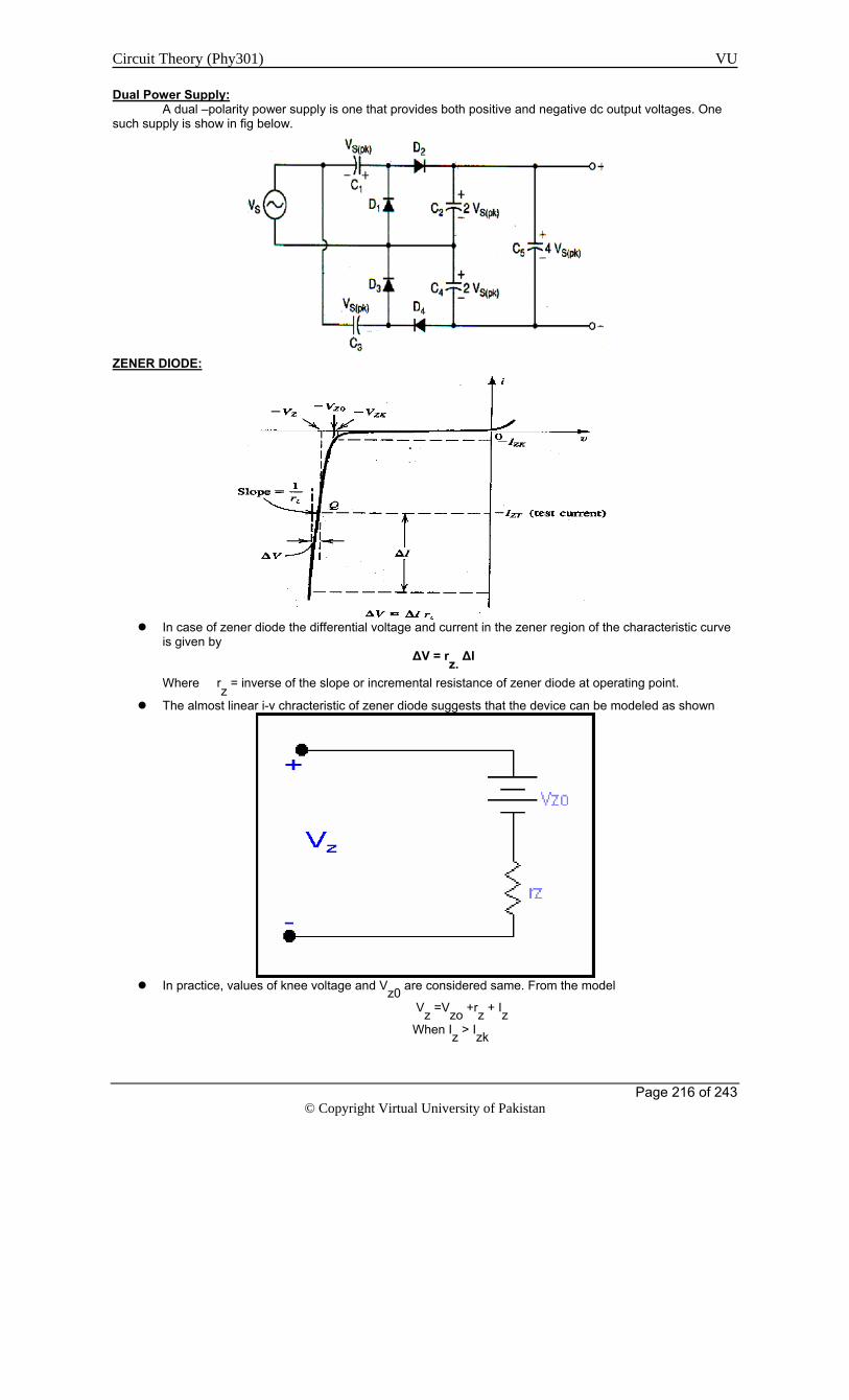
Circuit Theory (Phy301) VU
Page 216 of 243
© Copyright Virtual University of Pakistan
Dual Power Supply: A dual –polarity power supply is one that provides both positive and negative dc output voltages. One such supply is show in fig below.
ZENER DIODE:
In case of zener diode the differential voltage and current in the zener region of the characteristic curve
is given by ∆V = rz. ∆I
Where rz = inverse of the slope or incremental resistance of zener diode at operating point.
The almost linear i-v chracteristic of zener diode suggests that the device can be modeled as shown
In practice, values of knee voltage and Vz0 are considered same. From the model
Vz =Vzo +rz + Iz
When Iz > Izk

Circuit Theory (Phy301) VU
Page 217 of 243
© Copyright Virtual University of Pakistan
& Vz > Vzo
ZENER DIODE SHUNT REGULATOR: A regulator must posses two properties
(1) No change in V0 .with any change in Vs .
(2) No change in Vo with any change in I
L. Therefore two parameters are related as
(1) line regulation = ∆Vo/ ∆Vs
(2) Load regulation = ∆V0/ ∆IL Another method to describe these regulations

Circuit Theory (Phy301) VU
Page 218 of 243
© Copyright Virtual University of Pakistan
LECTURE 42 (Zener diode-LED-PIN Photodiodes - Tunnel diode) ZENER DIODE SHUNT REGULATOR:
From the circuit shown regulation = r
z/(R +r
z)
regulation = - rz || R
Current in the network =(Vs – V
z0)/R +r
z
Voltage across r
z is
Vrz
= V
z0 + (Vs – V
zo)r
z/(R +r
z)
Therefore applying Thevenin’s Theorem V
o = V
z0 + (V
s – V
z0)r
z/(R + r
z) x R
L/(R
L + R||r
z)
Therefore R x (Total current ) = Vsmin
– Vzo
– rzIzmin
Or R = (V
smin – V
z0 – r
zIzmin
)/(Izmin
+ ILmax
)
Example: A zener diode whose nominal voltage is 10V at 10mA has an incremental resistance of 50Ω. What voltage Ahmad Tulaib must expect if Bilal disturbs the settings to half the diode current. What is the value of V
zo of the zener model.
Solution: When the current is changed by -5mA, then voltage V
z=10 - r
zIz=10-5(0.05)=9.75V
When the current is doubled i.e. increased by 10mA, then V
z=10+10(0.05)=10.5V
Vzo
is the intercept of the tangent to characteristic at (10V,10mA) is the voltage change , when
the current decreases by 10mA, hence V
zo=10-10(0.05)=9.5V
Vzo
is the intercept of the tangent to characteristic at (10V,10mA) is the voltage change , when
the current decreases by 10mA, hence V
zo=10-10(0.05)=9.5V
Example: A zener diode exhibits a constant voltage of 5.6V for currents greater than five times the knee current I
zk is specified to be 1mA. It is to be used in the design of a shunt regulator fed from a
15V supply. The load current varies over the range 0 to 15mA. Find a suitable value for the resistance R. What is the maximum power dissipation to the zener diode. Solution:
The minimum Zener current is

Circuit Theory (Phy301) VU
Page 219 of 243
© Copyright Virtual University of Pakistan
Izk=5(1mA)=5mA
∵Load current may be 15mA, so that the value of R, is such that with IL=15mA, zener current of
5mA is available, therefore, R= (15-5.6)/20mA R = 470Ω The maximum power dissipated in the zener occurs when, I
L=0, in which case the zener current must
be 20mA, therefore P=20m(5.6)=112mW Example: A shunt regulator utilizes a zener diode whose voltage is 5.1Vat a current of 50mA and whose incremental resistance is 7Ω. The diode is fed from a supply of 15 V nominal voltages through a 200 Ω resistor. What is the output voltage at no load? Find the line regulation and load regulation. Solution:
Vzo=5.1-7(50m)
=4.75V At no load condition Vo= (15-4.75)7/207+4.75
=5.1V Line regulation=rz/(R+rz)
=7/207=33.8mV/V Load Regulation= - (r
z||R)
= -(7||200) = - 6.8Ω = -6.8mV/mA Example: Ghania is trying to design a shunt regulator, of about 20V, for her sister Azka’s toy. Two kinds of zener diodes are available: 6.8V devices with r
z of 10 Ω and 5.1V devices with r
z of 30 Ω. For the
two choices possible, find load regulation. In this calculation neglect the effect of regulator resistance R. Solution: Chioces a). In order make up 20V using 6.8V zener, three diodes will be needed, therefore 3x6.8=20.4V, so is the resistance, 3x10=30 Ω. Therefore load regulation, neglecting load resistance = -30 Ω. b). 4 diodes of 5.1 will make up 20.4 volts, therefore 4x5.1=20.4V, so is the resistance of the zener i.e. 4x30=120Ω. Load regulation (Neglecting R) = -120 Ω

Circuit Theory (Phy301) VU
Page 220 of 243
© Copyright Virtual University of Pakistan
Example: It is required to design a shunt regulator to provide a regulated voltage of about 10V. The available 10V, 1W zener of type !N4740 is specified to have a 10V drop at a test current of 25mA. At this current its r
z is 7 Ω. The raw supply available has a nominal value of 20Vbut can vary as much as
±25%. The regulator is required to supply a load current of 0 to 20mA. Design for a minimum zener current of 5mA. a). Find V
zo. b). Calculate the required value of R. c). Find the line regulation. What is the change in V
o expressed in %age,
corresponding to the ±25% change in Vs.
d). Find the load regulation. By what percentage does Vo change from no load to full load
condition. e). What is maximum current that the zener in your design should be able to conduct? What is the zener power dissipation under this condition? Solution: The provided data is V
z=10V, I
z=25mA, r
z=7Ω, V
s=20V±25%, I
zk=5mA, ∆I
L=20mA.
a). Vzo
=Vz-I
zrz=10-25m(7)=9.82V
b). Minimum current Izk
= 5mA will occur when Load current IL is maximum i.e. 20mA and V
s is
at minimum, so that Vs=20-5=15V.
Therefore
c). Line Regulation=∆V
o/ ∆V
s=r
z/(R+r
z)
7/212=33mV/V. ±25% change in V
s= ±5V
Therefore Vo
changes by ±5x33m
= ±165mV Percentage= ±0.165(100)/10= ±1.65%. d). Load Regulation=-r
z||R=-7||205
=-6.77Ω=-6.77V/A ∆V
o=-6.67(20m)=-135.4mV
Which in % =-135.4(100)/10=-1.35% e). Maximum zener current occurs at no load and V
s=20(1+0.25)=25V
Current=(25-9.825)/(205+7)=71.6mA Zener Power Dissipation =71.6m(10)=716mW Or more precisely V
z= 9.825+71.6m(7)=10.326V
Pz=71.6m (10.326)=739.4mW.

Circuit Theory (Phy301) VU
Page 221 of 243
© Copyright Virtual University of Pakistan
LIGHT EMITTING DIODES:
LED’s are diodes that will emit light when biased properly. The graphic symbol for an LED is shown in figure.
When sufficient voltage is applied to the chip across the leads of the LED, electrons can move easily in only one direction across the junction between the p and n regions. In the p region there are many more positive than negative charges. In the n region the electrons are more numerous than the positive electric charges. When a voltage is applied and the current starts to flow, electrons in the n region have sufficient energy to move across the junction into the p region. Once in the p region the electrons are immediately attracted to the positive charges due to the mutual Coulomb forces of attraction between opposite electric charges. When an electron moves sufficiently close to a positive charge in the p region, the two charges "re-combine". Each time an electron recombines with a positive charge; electric potential energy is converted into electromagnetic energy. For each recombination of a negative and a positive charge, a quantum of electromagnetic energy is emitted in the form of a photon of light with a frequency characteristic of the semi-conductor material (usually a combination of the chemical elements gallium, arsenic and phosphorus). Only photons in a very narrow frequency range can be emitted by any material. LED's that emit different colors are made of different semi-conductor materials, and require different energies to light them
LED’s are available in many of emitting colors as well as infrared (which is not visible), red, green, yellow, orange, and blue, the schematic symbol is the same for all colors. Since LED’s have clear cases, there is normally no label on the case to identify the leads.
The leads are normally in one of three ways (1) The leads may have different lengths. (2) One of the leads may be flattened. The flattened lead is usually the cathode.
(3) One side of the case may be flattened, the lead closest to the flattened side is usually the cathode. LED CHARACTERISTICS:
LED’s have characteristic curves that are very similar to those for pn junction diodes. However, they tend to have higher forward voltage (V
F) values and lower reverse break down voltage ratings. The
typical ranges for these values are as follows (1) Forward voltage: +1.2 to +4.3V (2) Reverse break down voltage : -3 to - 10V
PIN Photodiodes:
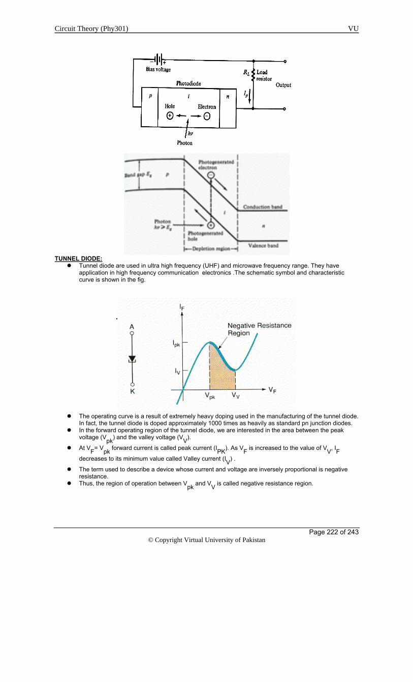
Circuit Theory (Phy301) VU
Page 222 of 243
© Copyright Virtual University of Pakistan
TUNNEL DIODE:
Tunnel diode are used in ultra high frequency (UHF) and microwave frequency range. They have application in high frequency communication electronics .The schematic symbol and characteristic curve is shown in the fig.
The operating curve is a result of extremely heavy doping used in the manufacturing of the tunnel diode.
In fact, the tunnel diode is doped approximately 1000 times as heavily as standard pn junction diodes. In the forward operating region of the tunnel diode, we are interested in the area between the peak
voltage (Vpk) and the valley voltage (VV).
At VF= Vpk forward current is called peak current (IPK). As VF is increased to the value of VV, IF
decreases to its minimum value called Valley current (IV) .
The term used to describe a device whose current and voltage are inversely proportional is negative resistance.
Thus, the region of operation between Vpk and VV is called negative resistance region.

Circuit Theory (Phy301) VU
Page 223 of 243
© Copyright Virtual University of Pakistan
LECTURE 43 (Bipolar Junction Transistor (BJT) BIPOLAR JUNCTION TRANSISTOR (BJT) CONSTRUCTION:
It is three layer semiconductor device, consisting of either two n- and one p-type layers of material or two p- and one n-type layers. Since three layers are involved in this device, therefore it will have three terminals. These terminals are known as:-
1. Emitter. 2. Base. 3. Collector.
Emitter layer is heavily doped. Base layer is lightly doped. Collector is very lightly doped. The base layer is very thin as compared to other two, normally in the range of 150:1.
The designated terminology for three terminals is as follows:- Emitter: This layer emits electrons. Base: It helps minority carriers to transfer rapidly from emitter to collector. Electric field is created in base by non-uniform doping, so that minority carriers are accelerated from emitter to collector. Collector: This layer collects the emitted electrons.
Two basic types of BJTs These types are in equation to constructional arrangement of layers. The arrangement shown in the figure is called NPN Transistor.
BIPOLAR JUNCTION TRANSISTOR THE SYMBOL FOR NPN TRANSISTOR: The arrow shows direction of flow of conventional current.

Circuit Theory (Phy301) VU
Page 224 of 243
© Copyright Virtual University of Pakistan
The arrangement is known as PNP transistor.
BIPOLAR JUNCTION TRANSISTOR THE SYMBOL FOR PNP TRANSISTOR:
BIPOLAR JUNCTION TRANSISTOR OPERATION IN PNP TRANSISTOR EMITTER BASE JUNCTION:
This fig shows the emitter base junction where emitter is made up of p-type material and Base is made up of N-type material .In the fig +ve terminal of the battery is connected to Emitter while –ve terminal is connected to the the Base. Its mean this junction will go in forward-biased condition and depletion layer will shrink. That is majority carriers will start crossing the junction of these particular layers. COLLECTOR BASE JUNCTION:
This fig shows the Collector-base junction where collector is made up of P-type material and Base is made up of N-type material .In the fig +ve terminal of the battery is connected to Base while –ve terminal is connected to the the Collector. Its mean this junction will go in to reverse-biased mode and depletion layer will be widened and the current will flow due to minority carriers.

Circuit Theory (Phy301) VU
Page 225 of 243
© Copyright Virtual University of Pakistan
In the fig above +ve terminal of the battery is connected to Emitter while –ve terminal of VEE is connected to the the Base while on the right side of this fig +ve terminal of the battery VCC is connected to Base while –ve terminal is connected to the the Collector. There are two depletion layers in the fig one is small while the other is bit wider and this is due to the forward biased of emitter-base junction and reverse biased due to the collector-base junction. We also see the emitter current IE will flow inward i:e. pointing into the transistor, however the base current IB and collector current IC is shown going outward from the transistor. OPERATING CONFIGURATIONS OF BJT:
There are three basic configurations under which transistor may be operated; these configurations depend upon the situation and requirements. These configurations are called
1. Common Base Configuration. 2. Common Emitter Configuration. 3. Common Collector Configuration.
COMMON BASE CONFIGURATION:
COMMON EMMITER CONFIGURATION:

Circuit Theory (Phy301) VU
Page 226 of 243
© Copyright Virtual University of Pakistan
COMMON COLLECTOR CONFIGURATION:
Directions of Currents in BJT:
MODES OF OPERATION OF BJT:
There are three modes of operation for BJT 1. Cut Off
When both the PN-junction of transistor are reverse –biased, the resulting mode of operation of the transistor in known as cut-off or simply as off-mode. This means that the BJT will be “OFF” and no current will flow through it. The fully supply voltage will exist across it. In everyday life an off switch will not permit any current to flow through an electric bulb and the full supply voltage will be present across the switch.
2. Active Mode When BEJ of a transistor is forward-biased but BCJ is reverse biased the mode of operation of a transistor is referred to as its active-mode. A bipolar junction transistor in its active-mode of operation is called as an amplifier and is able to amplify voltage or current signals both.
3. Saturation If both the PN-junctions , that is , the base-emitter junction (BEJ) and the base- collector junction (BCJ) are forward-biased, the transistor is said to be in its saturation (or ON) mode of operation. Graphical Presentation of BJT:
This curve has been drawn between the voltage across BEJ and the collector current. We can observe that the exponential rise in this collector current starts almost after 0.5 volts and saturated at 0.7 volts. Input or driving point characteristics Ic=IseV
BE / V
T

Circuit Theory (Phy301) VU
Page 227 of 243
© Copyright Virtual University of Pakistan
GRAPHICAL PRESENTATION OF BJT OUTPUT OR COLLECTOR CHARACTERISTIC FOR COMMON BASE CONFIGURATION:
Along x-axis we are taking VCE and along y-axis we are taking current collector current IC.
In the above fig below the 50 µ A is the cut off region of the transistor .Another shaded area along y- axis this area is a saturation region in this area we have maximum value of collector current i.e. IC exist while the value of VCE is minimum so in this area transistor will go in saturation. The un shaded area is called active region and it depends upon three parameters i.e. collector current base current and the applied voltage. MODES OF OPERATION OF BJT: EBJ CBJ
Cut Off Reverse Reverse Active Forward Reverse Saturation Forward Forward
For the transistors shown, state mode of operation.

Circuit Theory (Phy301) VU
Page 228 of 243
© Copyright Virtual University of Pakistan

Circuit Theory (Phy301) VU
Page 229 of 243
© Copyright Virtual University of Pakistan
LECTURE 44 (Bipolar Junction Transistor (BJT) THE CURRENTS OF A BJT:
1. The collector current. 2. The base Current. 3. The Emitter Current.
Collector Current
It can be expressed as IC=ISe(VBE/VT)
Is= saturation current or current scale factor.
The Base Current It is given by IB=IC/ β
Where β is a constant for particular transistor and is known as common emitter current gain, since IC/IB=β
The Emitter Current Since the total current which enters a transistor must leave it, hence we may write
IE=IB+IC But I
B=I
C/ β
Therefore, IE=IC+IC/ β
Or I
E= I
C(β+1)/ β
Or
IE
= Is e(VBE/VT)
(β+1)/ β
Alternatively, we may write I
C=αI
E α= β/ (β+1)
Or IE
=(Is/α) e
(VBE / VT)
Also we may write
α is known as common base current gain. Example: Show the transistor is in saturation.
β=α/(1-α)

Circuit Theory (Phy301) VU
Page 230 of 243
© Copyright Virtual University of Pakistan
SOLUTION:
For input loop, applying KVL 6 -V
BE- I
E(3.3k)=0
Rearranging IE
= (6-0.7)/3.3k=1.61mA
Therefore I
B= I
E/101=1.61m/101=15.94µA
Also VE
= IE
RE
=1.61m(3.3k)=5.3V
IC
=15.94 µ(100)=1.59mA
Therefore KVL Equation for the out put loop is 10-1.59m(4.7k)-V
C=0
∴ VC
=10-7.49=2.50V
∵VC
<VB
,
Hence the transistor is in saturation. DC BIASING-BJT:
1. Fixed bias circuit. 2. Emitter stabilized biased circuit. 3. Voltage divider bias.
DC BIASING-BJT: Fixed Bias Circuit

Circuit Theory (Phy301) VU
Page 231 of 243
© Copyright Virtual University of Pakistan
DC EQIVALENT OF THE CIRCUIT:
Forward bias of Base Emitter:
KVl Equation for the loop is V
CC-I
BR
B-V
BE = 0
or IB
= (VCC
-VBE
)/RB
Collector Emitter Loop:

Circuit Theory (Phy301) VU
Page 232 of 243
© Copyright Virtual University of Pakistan
Applying KVL V
CE+I
CR
C-V
CC= 0
or VCE
= VCC
-IC
RC
Also we may write V
CE=V
C-V
E ∵ V
E=0 in this case
∵ VCE
=VC
Also VBE
=VB
-VE
And VE
=0, thus
VBE
= VB
Example: Find IBQ and ICQ, VCEQ, VB, Vc, and VBC.Consider β=50.
SOLUTION:
Also we know that

Circuit Theory (Phy301) VU
Page 233 of 243
© Copyright Virtual University of Pakistan
LOAD LINE ANALYSIS:
The output equation of fixed bias circuit is given as V
CE = V
CC – I
CR
C
Which is an equation of a straight line. The corresponding x and y axes intercepts can be calculated by inserting appropriate values equal to zero. Therefore by putting IC = 0
We have VCE = VCC – (0)RC
VCE = VCC
Y intercept can be found by putting VCE = 0 volts so that
0 = VCC – ICRC
IC= VCC/RC Which defines the slop of the load line.

Circuit Theory (Phy301) VU
Page 234 of 243
© Copyright Virtual University of Pakistan
Example: Given a curve find Vcc,Rc,and RB for fixed bias circuit.

Circuit Theory (Phy301) VU
Page 235 of 243
© Copyright Virtual University of Pakistan
Solution: From the graph we have, for I
c=0
VCE
=VCC
=20V
Also at VCE
=0
IC
=VCC
/RC
R
C=V
CC/I
C=20/10m=2kΩ
Now IB
= (VCC
-VBE
)/RB
Or RB
= (Vcc
-VBE
)/IB
= (20-0.7)/25µ
= 772k Ω. DC BIASING-BJT: Emitter-Stabilized Bias Circuit
Base Emitter Loop

Circuit Theory (Phy301) VU
Page 236 of 243
© Copyright Virtual University of Pakistan
KVl Equation for the loop is VCC-IBRB-VBE-IERE=0
But IE=(β+1)IB
Therefore, VCC-IBRB-VBE-(β+1)IBRE=0
-IB(RB+(β+1)RE)+VCC-VBE=0
IB=(VCC-VBE)/(RB+(β+1)RE)
Collector-Emitter Loop
IERE+VCE+ICRC-VCC=0
But IE=Ic
VCE-Vcc+Ic(Rc+RE)=0
Vce=Vcc-Ic(Rc+RE)
Now VE is the voltage between the Emitter terminal and the ground, given by
VE=IERE Also Collector to ground voltage will be VCE=VC-VE
VC=VCE+VE Also Vc=VCC-IcRC Voltage at the base w.r.t ground will be VB=VCC-IBRB
VB=VBE+VE
Stabilization: Due to addition of the emitter resistance the values of DC bias currents and voltages remain constant with any changes in the Temperature and transistor beta.

Circuit Theory (Phy301) VU
Page 237 of 243
© Copyright Virtual University of Pakistan
LECTURE 45 (Bipolar Junction Transistor BJT-circuit analysis) Emitter-Stabilized Bias Circuit: Load Line Analysis
The collector emitter loop equation defining load line is V
CE=V
CC-I
C(R
C+R
E)
For IC
=0mA
VCE
=VCC
And for VCE
=0, we get
Ic=V
CC/(R
C+R
E)
Example: Zammad is designing an amplifier circuit as shown in the figure. Find the highest voltage to which the base can be raised while the transistor remains in active mode. Assume α=1.
Solution:
Lets consider that the voltage to which base can be raised for active operation be V. For the transistor to operate in active mode, consider V
B=V
C=V, therefore, for output loop, we have
10-4.7kIC
-VC
=0 (1)
Also for base-emitter loop we have V
B-V
BE-I
ER
E=0 (2)
∵α=1, therefore IC
=IE
From Equation (2) I
E=(V
B-V
BE)/R
E Putting the value of I
E in equation (1)

Circuit Theory (Phy301) VU
Page 238 of 243
© Copyright Virtual University of Pakistan
10-(V
B-V
BE)R
C/R
E-V
C= 0
10-(V-0.7)4.7/3.3-V = 0 3.3(10)-4.7V-3.29-V(3.3) =0 ∴ 8V=29.71 V=3.71V Example: For the circuit shown find RE & RC.
Solution: The given parameters are Ic=0.5mA & α=1, also V
CB=2V
Therefore, for the output loop we have by KVL (10-6)/0.5m=R
C R
C=8kΩ
∵α=1, Therefore, I
C=I
E=0.5mA
Hence for the base emitter loop by KVL (4-0.7)/0.5m=R
E R
E=6.6k Ω
DC BIASING-BJT: Voltage Divider Bias Circuit
The input loop of the circuit will be

Circuit Theory (Phy301) VU
Page 239 of 243
© Copyright Virtual University of Pakistan
Applying Thevenin’s theorem
RTh=R1IIR2
E
Th=V
R2=R
2V
cc/(R
1+R
2)
The Thévenin Equivalent circuit is

Circuit Theory (Phy301) VU
Page 240 of 243
© Copyright Virtual University of Pakistan
Therefore the KVL equation will be
Eth
-IB
RB
-VBE
-IE
R=0
Putting IE
=(β+1)IB
and solving for IB
IB
=(ETh—
VBE
)/(RTh
+(β+1)RE
)
Once IB
is known the remaining problem may be solved exactly as in the previous configurations.
Example: Find voltage at all nodes and current through all branches. Assume β=100.
Solution: Using Thevenin’s theorem the circuit takes the form as shown in the figure.

Circuit Theory (Phy301) VU
Page 241 of 243
© Copyright Virtual University of Pakistan
By writing VBB=15(RB2)/(RB1+RB2)
=15(50)/150=5V RBB=RB1||RB2 =100||50=33.3kΩ Writing the KVL equation for the loop L V
BB=I
BR
BB+V
BE+I
ER
E Put IB=IE/(β+1)
The base current will be I
B=1.29/101=0.0128mA
Therefore the base voltage will be V
B=V
BE+I
ER
E
=0.7+1.29(3)=4.57V
Assuming active mode the collector current will be I
C=αI
E=0.99(1.29)=1.28mA
And VC
=15-IC
RC
=15-1.28(5)=8.6V
Example: For the circuit shown find the voltages at all nodes and current through all branches.
Solution: Assume Q1 is in active mode, Therefore, from previous example VB1=4.57V
IE1=1.29mA
IB1=0.0128mA
IC1=1.28mA (assuming IB1 negligibly small)
Hence

Circuit Theory (Phy301) VU
Page 242 of 243
© Copyright Virtual University of Pakistan
VC1=15-Ic1RC1=15-(1.28)5=8.6V
Now assume that emitter base junction of Q2 is forward bias, hence VE2=VC1+VEB =8.6+0.7=9.3V Also IE2=(15-VE2)/RE2 =(15-9.3)/2k IE2=2.85mA
Now grounding of Q2 collector through RC2
shows, BC junction reverse bias
Ic2
=αIE2
=0.99(2.85m)
=2.82mA (β=100) ∴V
C2=I
c2R
c=7.62V
The value of Vc2
is lower than Vc1
=VB2
by 0.98V, therefore, Q2 is active.
Now errors I
B2=I
E2/(β
2+1)
=2.85m/101 =0.028mA Now doing iterations for I
c1 and I
B2 I
Rc1=I
c1-I
B2=1.25mA
Vc1=
15-5(1.252m)8.74V
VE2
=8.74+0.7=9.44V
IE2
=(15-9.44)/2k=2.78mA
Ic2
=0.99(2.78m)=2.75mA
Vc2
=2.75(2.7)=7.43V
IB2
=2.78/101=0.0275mA
Biasing using two power supplies:
The loop equation for the loop marked as L is

Circuit Theory (Phy301) VU
Page 243 of 243
© Copyright Virtual University of Pakistan
Example: The bias arrangement shown in the figure is to be used in common base amplifier. Design the circuit to establish a dc emitter current of 1mA and provide the highest possible gain while allowing for a maximum signal swing of ±2V at the collector. Use +10V and -5V power supplies.
Solution: Since the amplifier is to use in common base configuration, therefore the circuit will take the form as shown.
hence R
B=0
Considering the base-emitter junction forward biased, the emitter resistance can be found as R
E=(-0.7-(-5))/1m=4.3kΩ
In order to allow for ±2V signal swing at the collector, while choosing as larger value of RC as possible,
set VC=+2V, therefore -2V signal would not saturate the BJT. Thus
RC= (10-2)/IC
= 8/1mA RC = 8kΩ