VARISITE LTD. VAR SOM MX6 V í. ì Datasheet
52
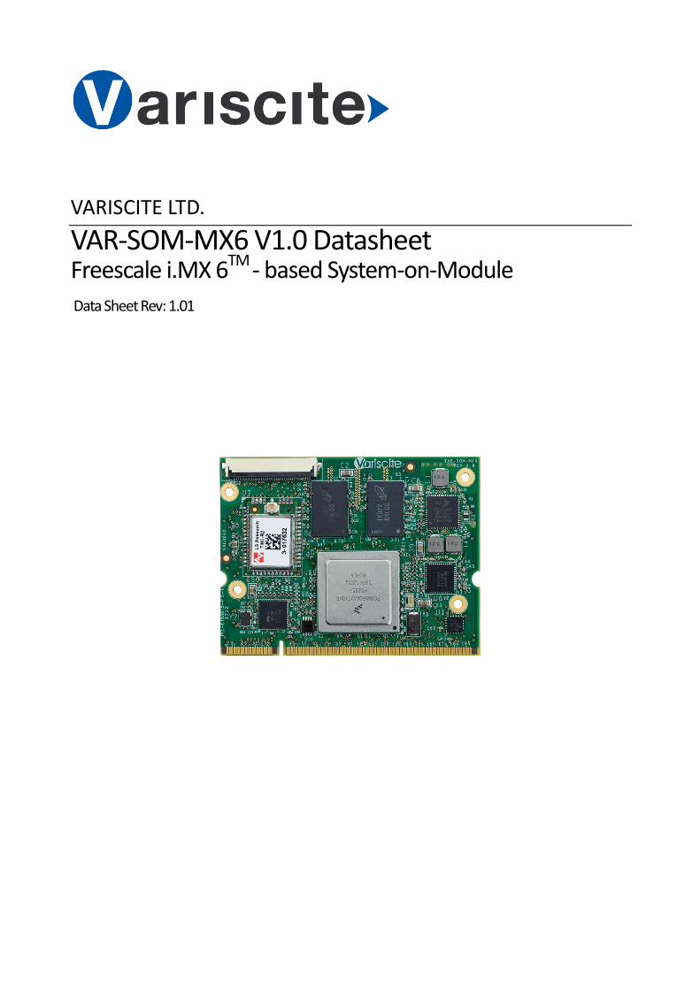
VARISCITE LTD. VAR-SOM-MX6 V1.0 Datasheet Freescale i.MX 6 TM - based System-on-Module Data Sheet Rev: 1.01
Transcript of VARISITE LTD. VAR SOM MX6 V í. ì Datasheet
VARISCITE LTD.
VAR-SOM-MX6 V1.0 Datasheet Freescale i.MX 6TM - based System-on-Module
Data Sheet Rev: 1.01

VARISCITE LTD.
VAR-SOM-MX6 Datasheet
© 2012 Variscite Ltd. All Rights Reserved. No part of this document may be photocopied, reproduced, stored in a retrieval system, or transmitted, in any form or by any means whether, electronic, mechanical, or otherwise without the prior written permission of Variscite Ltd. No warranty of accuracy is given concerning the contents of the information contained in this publication. To the extent permitted by law no liability (including liability to any person by reason of negligence) will be accepted by Variscite Ltd., its subsidiaries or employees for any direct or indirect loss or damage caused by omissions from or inaccuracies in this document. Variscite Ltd. reserves the right to change details in this publication without notice. Product and company names herein may be the trademarks of their respective owners.
Variscite Ltd. 9, Hamelacha Street Lod P.O.B 1121 Airport City, 70100 ISRAEL Tel: +972 (9) 9562910 Fax: +972 (9) 9589477

Document Revision History
Revision Date Notes 1.0 7/29/2012 Initial
1.01 10/22/2012 Minor text changes
Table of Contents Document Revision History ............................................................................................................................... iii
Table of Contents .............................................................................................................................................. iv
List of Tables ...................................................................................................................................................... 7
1. Overview ...................................................................................................................................................... 8
1.1. General Information ......................................................................................................................... 8 1.2. Feature Summary .............................................................................................................................. 9 1.3. Block Diagram ................................................................................................................................. 10
2. Main Hardware Components ..................................................................................................................... 11
2.1. Freescale i.MX 6 .............................................................................................................................. 11
2.1.1. Overview ................................................................................................................................. 11
2.1.2. i.MX 6 Block Diagram .............................................................................................................. 11
2.1.3. CPU Platform .......................................................................................................................... 12
2.1.4. Memory Interfaces ................................................................................................................. 12
2.1.5. DMA Engine ............................................................................................................................ 13
2.1.6. Display Subsystem .................................................................................................................. 13
2.1.7. MIPI - Camera Serial Interface Host Controller ...................................................................... 13
2.1.8. 2D and 3D Graphics Processing Unit (GPU) ........................................................................... 14
2.1.9. Audio Back End ....................................................................................................................... 15 2.1.10. 10/100/1000 Ethernet Controller ................................................................................................... 15 2.2. Memory........................................................................................................................................... 16
2.2.1. RAM ........................................................................................................................................ 16
2.2.2. Non-volatile Storage Memory ................................................................................................ 16 2.3. 10/100/1000 Ethernet PHY ............................................................................................................. 16 2.4. TLV320AIC3106 Audio ..................................................................................................................... 16 2.5. Wi-Fi + BT ........................................................................................................................................ 16 2.6. PMIC ............................................................................................................................................. 17
3. External Connectors ................................................................................................................................... 17
3.1. VAR-SOM-MX6 Connector Pin-out.................................................................................................. 18 3.2. SO-DIMM 200 Pin Mux ................................................................................................................... 23 3.3. 40-pin FFC Connector Pin-out ......................................................................................................... 25 3.4. 40-pin FFC Mux ............................................................................................................................... 27 3.5. Overview ......................................................................................................................................... 28 3.6. Display Interfaces ............................................................................................................................ 29
3.6.1. Overview ................................................................................................................................. 29
3.6.2. Interfaces ................................................................................................................................ 30 3.7. Touch Screen ................................................................................................................................... 33
3.7.1. Touch-screen Controller Signals ............................................................................................. 33 3.8. Camera Interfaces ........................................................................................................................... 33
3.8.1. MIPI CSI-2 ............................................................................................................................... 33
3.8.1.1. Signals ..................................................................................................................................... 34
3.8.2. CSIx ......................................................................................................................................... 34
3.8.3. CSI0 Signal............................................................................................................................... 34
3.8.4. CSI1 Signals ............................................................................................................................. 35
3.9. Gigabit Ethernet .............................................................................................................................. 36
3.9.1. Gigabit Ethernet Features ...................................................................................................... 36
3.9.2. Gigabit Ethernet Magnetics .................................................................................................... 36
3.9.3. Gigabit Ethernet Signals ......................................................................................................... 36 3.10. Wi-Fi & Bluetooth ........................................................................................................................... 36 3.11. USB Host 2.0.................................................................................................................................... 36
3.11.1. USB Host1 Signals ................................................................................................................... 37 3.12. USB 2.0 OTG .................................................................................................................................... 37
3.12.1. USB 2.0 On-the-go Features ................................................................................................... 37
3.12.2. OTG Signals ............................................................................................................................. 37 3.13. MMC/SD/SDIO ................................................................................................................................ 37
3.13.1. SDMMC1 Signals ..................................................................................................................... 38
3.13.2. SDMMC2 Signals ..................................................................................................................... 38 3.14. Audio ............................................................................................................................................. 38
3.14.1. Audio Features ....................................................................................................................... 38 3.15. UART Interfaces .............................................................................................................................. 39
3.15.1. UART Features ........................................................................................................................ 39
3.15.2. UART1 Signals ......................................................................................................................... 39
3.15.3. UART2 Signals ......................................................................................................................... 40
3.15.4. UART3 Signals ......................................................................................................................... 40
3.15.5. UART3 Signals ......................................................................................................................... 40 3.16. Flexible Controller Area Network (FLEXCAN) .................................................................................. 40
3.16.1. CAN1 Signals ........................................................................................................................... 41
3.16.2. CAN2 Signals ........................................................................................................................... 41 3.17. SPI ............................................................................................................................................. 41
3.17.1. ECSPI Key Features: ................................................................................................................ 41
3.17.2. ECSPI1 Signals ......................................................................................................................... 42
3.17.3. ECSPI2 Signals ......................................................................................................................... 42
3.17.4. ECSPI4 Signals ......................................................................................................................... 42 3.18. PCIE ............................................................................................................................................. 42
3.18.1. PCIE Signals ............................................................................................................................. 43 3.19. Serial ATA ........................................................................................................................................ 43
3.19.1. SATA Signals ............................................................................................................................ 43 3.20. I
2C ............................................................................................................................................. 43
3.20.1. I2C1 Signals ............................................................................................................................. 43
3.20.2. I2C2 Signals ............................................................................................................................. 43
3.20.3. I2C3 Signals ............................................................................................................................. 43 3.21. Local Bus ......................................................................................................................................... 44
3.21.1. Local Bus Signals SODIMM Connector .................................................................................... 44
3.21.2. Local Bus Signals 40 Pin FFC connector .................................................................................. 44 3.22. JTAG ............................................................................................................................................. 46
3.22.1. JTAG signals 40-pin FFC Connector ......................................................................................... 46 3.23. General Purpose IOs ....................................................................................................................... 46 3.24. General System Control .................................................................................................................. 46
3.24.1. Boot Options ........................................................................................................................... 46
3.24.2. Reset ....................................................................................................................................... 46
3.24.3. Reference Clock Out ............................................................................................................... 46
3.24.4. General System Control Signals .............................................................................................. 46 3.25. Power ............................................................................................................................................. 47
3.25.1. Power Supply .......................................................................................................................... 47
3.25.2. Ground .................................................................................................................................... 47
4. Absolute Maximum Characteristics ........................................................................................................... 48
5. Operational Characteristics ........................................................................................................................ 48
5.1. Power supplies ................................................................................................................................ 48 5.2. Power Consumption ....................................................................................................................... 48
6. DC Electrical Characteristics ....................................................................................................................... 48
7. Environmental Specifications ..................................................................................................................... 49
8. Mechanical Drawings ................................................................................................................................. 49
9. Legal Notice ................................................................................................................................................ 50
10. Warranty Terms ......................................................................................................................................... 51
11. Contact Information ................................................................................................................................... 52

List of Tables
Table 3-1 SO-DIMM200 Pin-out ............................................................................................................................................................. 23 Table 3-2 SO-DIMM 200 Pin Mux .......................................................................................................................................................... 25 Table 3-3 40 Pin FFC Pin Out .................................................................................................................................................................. 26 Table 3-4 40-pin FFC Mux Interface Details ........................................................................................................................................... 28 Table 3-5 DSI Signals .............................................................................................................................................................................. 31 Table 3-6 HDMI Signals .......................................................................................................................................................................... 31 Table 3-7 LVDS Signals ........................................................................................................................................................................... 32 Table 3-8 LVDS Signals ........................................................................................................................................................................... 33 Table 3-9 Touch-screen Signals ............................................................................................................................................................. 33 Table 3-10 CSI-2 Signals ......................................................................................................................................................................... 34 Table 3-11 CSI0 Signals .......................................................................................................................................................................... 35 Table 3-12 CSI1 Signals .......................................................................................................................................................................... 35 Table 3-13 Qualified Magnetics ............................................................................................................................................................. 36 Table 3-14 Gigabit Ethernet Signals ....................................................................................................................................................... 36 Table 3-15 USB Host1 Signals ................................................................................................................................................................ 37 Table 3-16 USB OTG Signals ................................................................................................................................................................... 37 Table 3-17 SDMMC1 Signals .................................................................................................................................................................. 38 Table 3-18 SDMMC2 Signals .................................................................................................................................................................. 38 Table 3-19 AUDMUX Signals .................................................................................................................................................................. 39 Table 3-20 SPDIF Signals ........................................................................................................................................................................ 39 Table 3-21 UART1 Signals ...................................................................................................................................................................... 40 Table 3-22 UART2 Signals ...................................................................................................................................................................... 40 Table 3-23 UART3 Signals ...................................................................................................................................................................... 40 Table 3-24 UART3 Signals ...................................................................................................................................................................... 40 Table 3-25 CAN1,2 Signals ..................................................................................................................................................................... 41 Table 3-26 CAN1,2 Signals ..................................................................................................................................................................... 41 Table 3-27 SPI1 Signals .......................................................................................................................................................................... 42 Table 3-28 SPI4 Signals .......................................................................................................................................................................... 42 Table 3-29 SPI4 Signals .......................................................................................................................................................................... 42 Table 3-30 PCIE Signals .......................................................................................................................................................................... 43 Table 3-31 SATA Signals ......................................................................................................................................................................... 43 Table 3-32 I2C1 Signals .......................................................................................................................................................................... 43 Table 3-33 I2C2 Signals .......................................................................................................................................................................... 43 Table 3-34 I2C3 Signals .......................................................................................................................................................................... 44 Table 3-35 Local Bus Signals SODIMM 200 Connector .......................................................................................................................... 44 Table 3-36 Local Bus Signals 40-pin FFC Connector ............................................................................................................................... 45 Table 3-37 JTAG Signals 40-pin FFC Connector ...................................................................................................................................... 46 Table 3-38 General System Signals ....................................................................................................................................................... 47
Table 3-39 Power Supply Pins ................................................................................................................................................................ 47 Table 3-40 Ground Pins ......................................................................................................................................................................... 47 Table 4-1 Absolute Maximum Characteristics ....................................................................................................................................... 48 Table 5-1 Power Supplies Operational Characteristics .......................................................................................................................... 48 Table 6-1 DC Electrical Characteristics ................................................................................................................................................... 48 Table 7-1 Environment Specifications ................................................................................................................................................... 49
V A R - S O M - M X 6 V 1 . 0 S Y S T E M O N M O D U L E
1. Overview 1.1. General Information
The VAR-SOM-MX6 is a high performance System-on-Module. It provides an ideal building block that easily integrates with a wide range of target markets requiring rich multimedia functionality, powerful graphics and video capabilities, as well as high-processing power. Compact, cost effective and with low power consumption, VAR-SOM-MX6 secures an Intel Atom performance level.
Supporting products:
VAR-MX6CustomBoard – evaluation board
Carrier -Board, compatible with VAR-SOM-MX6
Schematics
VAR-EXT-CB402 – CSI2 Camera module
O.S support
Linux BSP
Windows Embedded Compact 7
Android
Contact Variscite support services for further information: mailto:[email protected].
V A R - S O M - M X 6 S Y S T E M O N M O D U L E
9
1.2. Feature Summary
• Freescale i.MX 6 series SoC (Single/Dual /Quad ARM® Cortex™-A9 Core, 1.2 GHz)
• Up to 16 Gb DDR3 RAM
• 8Gb NAND Flash for storage memory/boot
• 2 x LVDS display interface
• HDMI V1.4 interface
• 1 x MIPI DSI
• Touch panel interface
• Parallel & serial camera interface
• On-board 10/100/1000 Mbps Ethernet PHY
• WLAN (802.11 b/g/n) / BT
• 1 x USB 2.0 host, 1 x OTG
• 2 x SD/MMC
• Serial interfaces ( SPI , I2C, UART, I2S,)
• CAN Bus
• Stereo line-In/out
• Digital microphone
• Single 3.3 V power supply
• 67mm x 51mm, 200 pin SO-DIMM Connector

V A R - S O M - M X 6 S Y S T E M O N M O D U L E
10
1.3. Block Diagram

V A R - S O M - M X 6 S Y S T E M O N M O D U L E
11
2. Main Hardware Components This section summarizes the main hardware building blocks of the VAR-SOM-MX6
2.1. Freescale i.MX6
2.1.1. Overview
The i.MX 6Dual and i.MX 6 Quad processors represent Freescale Semiconductor’s latest achievement in integrated multimedia applications processors, optimized for lowest power consumption. The processors feature Freescale’s advanced implementation of the quad ARM™ Cortex-A9 core, which operates at speeds of up to 1.2 GHz. They include 2D and 3D graphics processors, 3D 1080p video processing and integrated power management. Each processor provides a 64-bit DDR3/LVDDR3-1066 memory interface and a number of other interfaces such as WLAN, Bluetooth™, GPS, hard drive, displays, and camera sensors.
2.1.2. i.MX 6 Block Diagram
V A R - S O M - M X 6 S Y S T E M O N M O D U L E
12
2.1.3. CPU Platform
The i.MX 6 Dual / Quad Application Processor (AP) is based on the ARM Cortex-A9 MPCore™ Platform, which has the following features: • ARM Cortex A9 MPCore™ Dual or Quad core CPU configurations (with TrustZone)
• Symmetric CPU configuration where each CPU includes:
- 32 Kbyte L1 Instruction Cache
- 32 Kbyte L1 Data Cache
- Private Timer and Watchdog
- Cortex-A9 NEON MPE (Media Processing Engine) Co-processor.
• The ARM Cortex A9 MPCore™ complex includes:
- General Interrupt Controller (GIC) with 128 interrupt support
- Global Timer
- Snoop Control Unit (SCU)
- 1 Megabyte unified L2 cache shared by all CPU cores (Dual or Quad)
- Two Master AXI (64-bit) bus interfaces output of L2 cache
• NEON MPE coprocessor
- SIMD Media Processing Architecture
- NEON register file with 32x64-bit general-purpose registers
- NEON Integer execute pipeline (ALU, Shift, MAC)
- NEON dual, single-precision floating point execute pipeline (FADD, FMUL)
- NEON load/store and permute pipeline External
- Supports single and double-precision add, subtract, multiply, divide, multiply and
accumulate, and square root operations as described in the ARM VFPv3
architecture.
• Provides conversions between 16-bit, 32-bit and 64-bit floating-point formats and ARM
integer word formats.
2.1.4. Memory Interfaces
The memory system consists of the following components: • Level 1 Cache—32 KB Instruction, 32 KB Data cache per core
• Level 2 Cache—Unified instruction and data (1 MByte)
• On-Chip Memory:
- Boot ROM, including HAB (96 KB)
- Internal multimedia / shared, fast access RAM (OCRAM, 256 KB)
- Secure/non-secure RAM (16 KB)
• External memory interfaces:
- 16-bit, 32-bit, and 64-bit DDR3-1066, LV-DDR3-1066, and 1/2 LPDDR2-1066
channels, supporting DDR interleaving mode, for 2x32 LPDDR2-1066
- 8-bit NAND-Flash, including support for Raw MLC/SLC, 2 KB, 4 KB, and 8 KB page
size,
- BA-NAND, PBA-NAND, LBA-NAND, OneNAND™ and others. BCH ECC up to 32 bit.
- 16-bit NOR Flash. All WEIMv2 pins are muxed on other interfaces.
- 16-bit PSRAM, Cellular RAM
V A R - S O M - M X 6 S Y S T E M O N M O D U L E
13
2.1.5. DMA engine
The SDMA is multi-channel flexible DMA engine. It helps in maximizing system performance by off-loading the various cores in dynamic data routing. It has the following features: • Powered by a 16-bit Instruction-Set micro-RISC engine
• Multi-channel DMA supporting up to 32 time-division multiplexed DMA channels
• 48 events with total flexibility to trigger any combination of channels
• Memory accesses including linear, FIFO, and 2D addressing
• Shared peripherals between ARM and SDMA
• Very fast Context-Switching with 2-level priority based preemptive multi-tasking
• DMA units with auto-flush and prefetch capability
• Flexible address management for DMA transfers (increment, decrement, and no
address changes on source and destination address)
• DMA ports can handle unit-directional and bi-directional flows (copy mode)
• Up to 8-word buffer for configurable burst transfers
• Support of byte-swapping and CRC calculations
• Library of Scripts and API is available
2.1.6. Display Subsystem
The i.MX 6Dual/6Quad video graphics subsystem consists of the following dedicated modules: • Video Processing Unit (VPU): a multi-standard high performance video/image CODEC
• Three Graphics Processing Units (GPUs):
- 3D GPU: accelerating the generation of 3D graphics (OpenGL/ES) and vector graphics
(OpenVG)
- 2D GPU: acceleration the generation of 2D graphics (BitBLT).
- OpenVG: acceleration of vector graphics (OpenVG).
• Two (identical) Image Processing Units (IPUs): providing connectivity to cameras and
displays, related processing, synchronization and control.
• Display interface bridges: providing optional translation from the digital display interface
supported by the IPU to other interfaces:
- LVDS bridge (LDB): providing up to two LVDS interfaces
- HDMI transmitter
- MIPI/DSI transmitter
• MIPI/CSI-2 receiver
• Two (identical) Display Content Integrity Checker (DCIC) are used to authenticate
sensitive displayed data.
• A Video Data Order Adapter (VDOA): used to re-order video data from the "tiled" order
used by the VPU to the conventional raster-scan order needed by the IPU.
2.1.7. MIPI - Camera Serial Interface Host Controller
The MIPI CSI-2 Host Controller supports the following features:
V A R - S O M - M X 6 S Y S T E M O N M O D U L E
14
• Compliant with MIPI Alliance Standard for Camera Serial Interface 2 (CSI-2), Version 1.00
- 29 November 2005
• Optional support for Camera Control Interface (CCI) through the use of DesignWare Core
(DW_apb_i2c)
• Interface with MIPI D-PHY following PHY Protocol Interface (PPI), as defined in MIPI
Alliance Specification for D-PHY, Version 1.00.00 - 14 May 2009
• Supports up to 4 D-PHY Rx Data Lanes
• Dynamically configurable multi-lane merging
• Long and Short packet decoding
• Timing accurate signaling of Frame and Line synchronization packets; Support for several
frame formats such as:
- General Frame or Digital Interlaced Video with or without accurate sync timing
- Data type (Packet or Frame level) and Virtual Channel interleaving
• 32-bit Image Data Interface delivering data formatted as recommended in CSI-2
Specification
• Supports all primary and secondary data formats:
- RGB, YUV and RAW color space definitions
- From 24-bit down to 6-bit per pixel
- Generic or user-defined byte-based data types
- Error detection and correction
- PHY level
- Packet level
- Line level
- Frame level
2.1.8. 2D and 3D Graphics Processing Unit (GPU)
The GPU2D module has two independent sub-modules: R2D and V2D GPUs. Both GPU were designed to display on a variety of consumer devices. Addressable screen sizes range from small displays featured on cell phones to large 1080p high definition displays. The GPU2D cores provide powerful graphics at low power consumption, utilizing the smallest silicon footprints. Dynamic power consumption is minimized by extensive use of localized clock gating. Hardware acceleration is brought to numerous 2D and VG applications including graphical user interfaces (GUI), menu displays, flash animation and gaming. The GPU3D is a high-performance core that delivers hardware acceleration for 3D graphics display. Addressable screen sizes range from the smallest cell phones to HD 1080p displays. It provides high performance, high quality graphics, low power consumption and the smallest silicon footprint. GPU3D accelerates numerous 3D graphics applications, including Graphical User Interfaces (GUI), menu displays, flash animation, and gaming. This module supports the following graphics APIs: • OpenGL ES 2.0
• OpenGL ES 1.1
• OpenVG 1.1
• EGL 1.4
• DirectX 11_9_3
V A R - S O M - M X 6 S Y S T E M O N M O D U L E
15
• OpenGL 2.1 and 3.0
• OpenCL 1.1 E
2.1.9. Audio Back End
The AUDMUX provides flexible, programmable routing of the serial interfaces (SSI1 or SSI2) to and from off-chip devices. The AUDMUX routes audio data (and even splices together multiple time-multiplexed audio streams) but does not decode or process audio data itself. The AUDMUX is controlled by the ARM but can route data even when the ARM is in a low-power mode. The ESAI (Enhanced Serial Audio Interface) provides a full-duplex serial port for serial communication with a variety of serial devices, including industry-standard codecs, SPDIF transceivers, and other processors. The ESAI consists of independent transmitter and receiver sections, each section with its own clock generator. The ESAI is connected to the IOMUX and to the ESAI_BIFIFO module. The ESAI_BIFIFO (ESAI Bus Interface and FIFO) is the interface between the ESAI module and the shared peripheral bus. It contains the FIFOs used to buffer data to and from the ESAI, as well as providing the data word alignment and padding necessary to match the 24-bit data bus of the ESAI to the 32-bit data bus of the shared peripheral bus. The SPDIF (Sony/Philips Digital Interface) audio module is a stereo transceiver that allows the processor to receive and transmit digital audio over it. The SPDIF receiver section includes a frequency measurement block that allows the precise measurement of incoming sampling frequency. A recovered clock is provided by the SPDIF receiver section and may be used to drive both internal and external components in the system. The SPDIF is connected to the shared peripheral bus. The ASRC (Asynchronous Sample Rate Converter) converts the sampling rate of a signal associated to an input clock into a signal associated to a different output clock. The ASRC supports concurrent sample rate conversions of up to 10 channels of over 120dB THD+N. The sample rate conversion of each channel is associated to a pair of incoming and outgoing sampling rates. The ASRC supports up to three sampling rate pairs. The ASRC is connected to the shared peripheral bus.
2.1.10. 10/100/1000 Ethernet Controller
The MAC-NET core, in conjunction with a 10/100/1000 MAC, implements layer 3 network acceleration functions. These functions are designed to accelerate the processing of various common networking protocols, such as IP, TCP, UDP and ICMP, providing wire speed services to client applications. The MAC operation is fully programmable and can be used in NIC (Network Interface Card), bridging, or switching applications. The core implements the remote network monitoring (RMON) counters according to IETF RFC 2819. The core also implements a hardware acceleration block to optimize the performance of network controllers providing IP and TCP, UDP, ICMP protocol services. The acceleration block performs critical functions in hardware, which are typically implemented with large software overhead. The core implements programmable embedded FIFOs that can provide buffering on the receive path for loss-less flow control .Advanced power management features are available with magic packet detection and programmable power-down modes.
V A R - S O M - M X 6 S Y S T E M O N M O D U L E
16
2.2. Memory
2.2.1. RAM
The VAR-SOM-MX6 is available with up to 16 Gb of DDR3 memory.
2.2.2. Non-volatile Storage Memory
The VAR-SOM-MX6 is available with up to 8 Gb of NAND FLASH memory. The NAND flash is used for Flash Disk purposes, O.S. run-time-image and the Boot-loader (Boot from NAND). First block (block address 00h) of the memory device is guaranteed to be valid without ECC (up to 1,000 PROGRAM/ERASE cycles)
2.3. 10/100/1000 Ethernet PHY
The VAR-SOM-MX6 features the Micrel KSZ9031 gigabit Ethernet PHY. The KSZ9031RN is a completely integrated triple speed (10Base-T/100Base-TX/1000Base-T) Ethernet Physical Layer Transceiver for transmission and reception of data over standard CAT-5 unshielded twisted pair (UTP) cable. The KSZ9031RN provides the Reduced Gigabit Media Independent Interface (RGMII) for direct connection to RGMII MACs in Gigabit Ethernet processors and switches for data transfer at 10/100/1000 Mbps speed.
2.4. TLV320AIC3106 Audio
The Texas Instrument’s TLV320AIC3106 is a low-power, highly integrated stereo audio codec with stereo headphone amplifier, as well as multiple inputs and outputs programmable in single-ended or fully differential configurations. Extensive register-based power control is included, enabling stereo 48-kHz DAC playback as low as 15mW. The VAR-SOM-MX6 exposes the following interface of the TLV320AIC3106:
Headphone
Line-in
Digital microphone
2.5. Wi-Fi + BT
Wi-Fi & Bluetooth connectivity is supported by an on-board module TiWi – R2. The TiWi-R2 module is a high performance 2.4 GHz IEEE 802.11 b/g/n Bluetooth 2.1+EDR radio in a cost effective, pre-certified footprint. The module realizes the necessary PHY/MAC layers to support WLAN applications in conjunction with a host processor over a SDIO interface. The module also provides a Bluetooth platform through the HCI transport layer. Both WLAN and Bluetooth share the same antenna port.
V A R - S O M - M X 6 S Y S T E M O N M O D U L E
17
2.6. PMIC
The VAR-SOM-MX6 features Freescale’s PMPF0100 as a Power Management Integrated circuit (PMIC) designed specifically for use with Freescale’s i.MX6 series of application processors. The PMPF0100 regulates all power rails required on SoM from a single 3.3 V power supply. The PMIC is fully programmable via the I2C interface and associated register map. Additional communication is provided by direct logic interfacing including interrupt, watchdog and reset.
3. External Connectors
The VAR-SOM-MX6 exposes a 200-pin SO–DIMM mechanical standard interface. The recommended mating connector for baseboard interfacing is FCI 10033853-052FSLF or equivalent. In addition to 200-pin SO-DIMM interface VAR-SOM-MX6 exposes a 40-pin FFC connector. The recommended mating cable is Molex 21020-0427 or equivalent. The following list describes this chapter’s column header tables: Pin#: Pin number on the SO-DIMM200 connector Pin Name: Default VAR-SOM-MX6 pin name Type: Pin type & direction:
I – In
O – Out
DS – Differential Signal
A – Analog
Power – Power Pin
Pin Group: Pin functionality group
i.MX6 Ball: Ball number Mode (Tables 3.2 & 3.4): Pin mux mode option
V A R - S O M - M X 6 S Y S T E M O N M O D U L E
18
3.1. VAR-SOM-MX6 Connector Pin-out
Pin #
Pin Name
Type
Pin Group
GPIO i.MX6 Ball
1 GND POWER Digital GND
2 GND POWER Digital GND
3 MDI_A+ DS
Gigabit Ethernet
4 MDI_C+ DS Gigabit Ethernet
5 MDI_A- DS
Gigabit Ethernet
6 MDI_C- DS Gigabit Ethernet
7 GND POWER
Digital GND
8 GND POWER Digital GND
9 MDI_B+ DS
Gigabit Ethernet
10 MDI_D+ DS Gigabit Ethernet
11 MDI_B- DS
Gigabit Ethernet
12 MDI_D- DS Gigabit Ethernet
13 GND POWER
Digital GND
14 GND POWER Digital GND
15 GETH_LED2 O
Gigabit Ethernet LED
16 GETH_LED1 O Gigabit Ethernet LED
17 PWM0 IO
Pulse width modulation GPIO4[30] T25
18 DMIC_CLK O Digital microphone interface
19 GND POWER
Digital GND
20 DMIC_DATA I Digital microphone interface
21 AUDMUX4_RXD IO
Digital audio mux GPIO5[17] W24
22 AUDMUX4_RXC IO Digital audio mux
GPIO5[13] U23
23 AUDMUX4_RXFS IO
Digital audio mux GPIO5[12] V25
24 AUDMUX4_TXFS
IO Digital audio mux
GPIO5[16] V24
25 AUDMUX4_TXC IO
Digital audio mux GPIO5[14] U22
26 AUDMUX4_TXD IO Digital audio mux
GPIO5[15] T20
27 GND POWER Digital GND
28 GND POWER Digital GND
29 CLKO2 O
Reference clock out
30 NC Leave not connected
31 GND POWER
Digital GND
32 VIN_3V3 POWER 3.3 V power supply IN
33 GND POWER
Digital GND
34 VIN_3V3 POWER 3.3 V power supply IN
35 GND POWER
Digital GND
36 VIN_3V3 POWER 3.3 V power supply IN
37 GND POWER
Digital GND
38 VIN_3V3 POWER 3.3 V power supply IN
V A R - S O M - M X 6 S Y S T E M O N M O D U L E
19
Pin #
Pin Name
Type
Pin Group
GPIO i.MX6 Ball
39 CSPI1_CS0 IO
Configurable SPI GPIO4[9] U6
40 BOOT_SEL1 IO
GPIO3[13] M23
41 CSPI1_MISO IO
Configurable SPI GPIO4[8] U7
42 BOOT_SEL0 IO
43 CSPI1_CLK IO
Configurable SPI GPIO4[6] W5
44 CAN1_TX IO Controller area network
GPIO1[7] R3
45 CSPI1_MOSI IO
Configurable SPI GPIO4[7] V6
46 CAN1_RX IO Controller area network
GPIO1[8] R5
47 GND POWER
Digital GND
48 CSPI1_CS1 IO Configurable SPI
GPIO4[10] W6
49 3V3_PER POWER
Power good indication
50 UART2_CTS IO UART2 port
[2]
GPIO3[28] G23
51 UART2_RTS IO
UART2 port[2]
GPIO3[29] J19
52 UART2_TXD IO UART2 port
[2]
GPIO3[24] F22
53 UART2_RXD IO
UART2 port[2]
GPIO3[27] E25
54 UART3_RXD IO UART3 port
GPIO3[25] G22
55 UART3_CTS IO
UART3 port GPIO3[23] D25
56 UART3_TXD IO UART3 port
GPIO2[30] E22
57 UART3_RTS IO
UART3 port GPIO2[31] F23
58 GND POWER Digital GND
59 GND POWER
Digital GND
60 SD2_CLK IO SD/MMC and SDXC
61 SD2_DATA2 IO
SD/MMC and SDXC GPIO1[13] A23
62 SD2_DATA0 IO SD/MMC and SDXC
GPIO1[15] A22
63 SD2_DATA1 IO
SD/MMC and SDXC GPIO1[14] E20
64 SD2_CMD O SD/MMC and SDXC
GPIO1[11] F19
65 SD2_DATA3 IO
SD/MMC and SDXC GPIO1[12] B22
66 GND POWER Digital GND
67 GND POWER
Digital GND
68 SD1_DATA0 IO SD/MMC and SDXC
GPIO1[16] A21
69 SD1_CMD IO
SD/MMC and SDXC GPIO1[18] B21
70 SD1_DATA2 IO SD/MMC and SDXC
GPIO1[19] E19
71 SD1_DATA1 IO
SD/MMC and SDXC GPIO1[17] C20
72 SD1_CLK O SD/MMC and SDXC
73 SD1_DATA3 IO
SD/MMC and SDXC GPIO1[21] F18
74 NC Leave not connected
75 SPDIFIN IO
SPDIF GPIO3[21] H20
76 GND POWER Digital GND
77 SPDIFOUT IO
SPDIF GPIO3[22] E23
V A R - S O M - M X 6 S Y S T E M O N M O D U L E
20
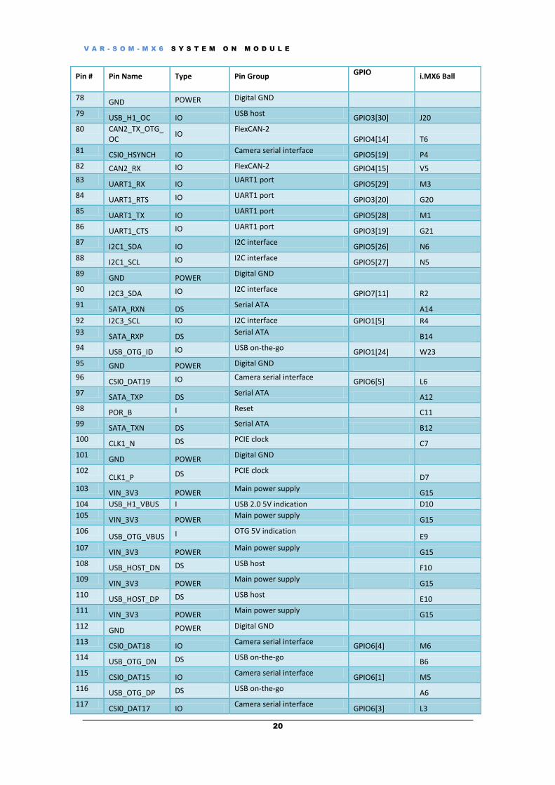
Pin #
Pin Name
Type
Pin Group
GPIO i.MX6 Ball
78 GND POWER Digital GND
79 USB_H1_OC IO
USB host GPIO3[30] J20
80 CAN2_TX_OTG_OC
IO FlexCAN-2
GPIO4[14] T6
81 CSI0_HSYNCH IO
Camera serial interface GPIO5[19] P4
82 CAN2_RX IO FlexCAN-2 GPIO4[15] V5
83 UART1_RX IO
UART1 port GPIO5[29] M3
84 UART1_RTS IO UART1 port
GPIO3[20] G20
85 UART1_TX IO
UART1 port GPIO5[28] M1
86 UART1_CTS IO UART1 port
GPIO3[19] G21
87 I2C1_SDA IO
I2C interface GPIO5[26] N6
88 I2C1_SCL IO I2C interface
GPIO5[27] N5
89 GND POWER
Digital GND
90 I2C3_SDA IO I2C interface
GPIO7[11] R2
91 SATA_RXN DS
Serial ATA A14
92 I2C3_SCL IO I2C interface GPIO1[5] R4
93 SATA_RXP DS
Serial ATA B14
94 USB_OTG_ID IO USB on-the-go
GPIO1[24] W23
95 GND POWER Digital GND
96 CSI0_DAT19 IO Camera serial interface
GPIO6[5] L6
97 SATA_TXP DS
Serial ATA A12
98 POR_B I Reset C11
99 SATA_TXN DS
Serial ATA B12
100 CLK1_N DS PCIE clock
C7
101 GND POWER
Digital GND
102 CLK1_P DS PCIE clock
D7
103 VIN_3V3 POWER
Main power supply G15
104 USB_H1_VBUS I USB 2.0 5V indication D10
105 VIN_3V3 POWER
Main power supply G15
106 USB_OTG_VBUS I OTG 5V indication
E9
107 VIN_3V3 POWER
Main power supply G15
108 USB_HOST_DN DS USB host
F10
109 VIN_3V3 POWER
Main power supply G15
110 USB_HOST_DP DS USB host
E10
111 VIN_3V3 POWER
Main power supply G15
112 GND POWER Digital GND
113 CSI0_DAT18 IO
Camera serial interface GPIO6[4] M6
114 USB_OTG_DN DS USB on-the-go
B6
115 CSI0_DAT15 IO
Camera serial interface GPIO6[1] M5
116 USB_OTG_DP DS USB on-the-go
A6
117 CSI0_DAT17 IO
Camera serial interface GPIO6[3] L3
V A R - S O M - M X 6 S Y S T E M O N M O D U L E
21
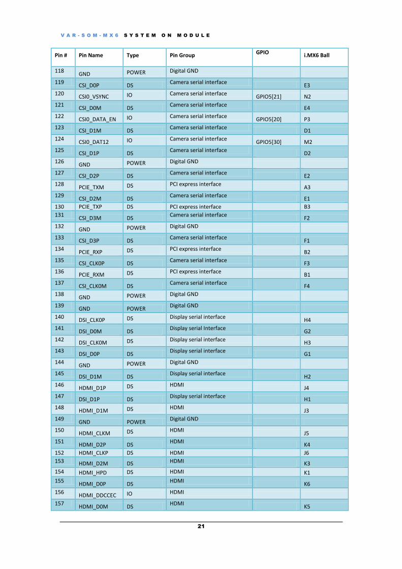
Pin #
Pin Name
Type
Pin Group
GPIO i.MX6 Ball
118 GND POWER Digital GND
119 CSI_D0P DS
Camera serial interface E3
120 CSI0_VSYNC IO Camera serial interface
GPIO5[21] N2
121 CSI_D0M DS
Camera serial interface E4
122 CSI0_DATA_EN IO Camera serial interface
GPIO5[20] P3
123 CSI_D1M DS
Camera serial interface D1
124 CSI0_DAT12 IO Camera serial interface
GPIO5[30] M2
125 CSI_D1P DS
Camera serial interface D2
126 GND POWER Digital GND
127 CSI_D2P DS
Camera serial interface E2
128 PCIE_TXM DS PCI express interface
A3
129 CSI_D2M DS
Camera serial interface E1
130 PCIE_TXP DS PCI express interface B3
131 CSI_D3M DS
Camera serial interface F2
132 GND POWER Digital GND
133 CSI_D3P DS
Camera serial interface F1
134 PCIE_RXP DS PCI express interface
B2
135 CSI_CLK0P DS
Camera serial interface F3
136 PCIE_RXM DS PCI express interface
B1
137 CSI_CLK0M DS
Camera serial interface F4
138 GND POWER Digital GND
139 GND POWER
Digital GND
140 DSI_CLK0P DS Display serial interface
H4
141 DSI_D0M DS
Display serial Interface G2
142 DSI_CLK0M DS Display serial interface
H3
143 DSI_D0P DS
Display serial interface G1
144 GND POWER Digital GND
145 DSI_D1M DS
Display serial interface H2
146 HDMI_D1P DS HDMI
J4
147 DSI_D1P DS
Display serial interface H1
148 HDMI_D1M DS HDMI
J3
149 GND POWER
Digital GND
150 HDMI_CLKM DS HDMI
J5
151 HDMI_D2P DS
HDMI K4
152 HDMI_CLKP DS HDMI J6
153 HDMI_D2M DS HDMI K3
154 HDMI_HPD DS HDMI K1
155 HDMI_D0P DS
HDMI K6
156 HDMI_DDCCEC IO HDMI
157 HDMI_D0M DS
HDMI K5

V A R - S O M - M X 6 S Y S T E M O N M O D U L E
22
Pin #
Pin Name
Type
Pin Group
GPIO i.MX6 Ball
158 GND POWER Digital GND
159 GND POWER
Digital GND
160 LVDS0_TX1_N DS LVDS display bridge U4
161 LVDS0_TX0_N DS
LVDS display bridge U2
162 LVDS0_TX1_P DS LVDS display bridge
U3
163 LVDS0_TX0_P DS
LVDS display bridge U1
164 LVDS0_TX2_N DS LVDS display bridge
V2
165 LVDS0_TX3_N DS
LVDS display bridge W2
166 LVDS0_TX2_P DS LVDS display bridge
V1
167 LVDS0_TX3_P DS
LVDS display bridge W1
168 LVDS0_CLK_N DS LVDS display bridge
V3
169 GND POWER
Digital GND
170 LVDS0_CLK_P DS LVDS display bridge
V4
171 CSI0_DAT14 IO
Camera serial interface GPIO6[0] M4
172 GND POWER Digital GND
173 CSI0_DAT16 IO
Camera serial interface GPIO6[2] L4
174 I2C2_SCL IO I2C interface
[1]
175 CSI0_DAT13 IO
Camera serial interface GPIO5[31] L1
176 I2C2_SDA IO I2C interface
[1]
177 CSI0_PIXCLK I
Camera serial interface
178 GND POWER Digital GND
179 GND POWER
Digital GND
180 LVDS1_CLK_N DS LVDS display bridge
Y3
181 LVDS1_TX3_P DS
LVDS display bridge AA4
182 LVDS1_CLK_P DS LVDS display bridge
Y4
183 LVDS1_TX3_N DS
LVDS display bridge AA3
184 LVDS1_TX0_N DS LVDS display bridge
Y1
185 GND POWER
Digital GND
186 LVDS1_TX0_P DS LVDS display bridge Y2
187 TS_X- AI
Touch screen interface
188 LVDS1_TX1_N DS LVDS display bridge
AA1
189 TS_X+ AI
Touch screen interface
190 LVDS1_TX1_P DS LVDS display bridge
AA2
191 TS_Y+ AI
Touch screen interface
192 LVDS1_TX2_N DS LVDS display bridge
AB1
193 TS_Y- AI
Touch screen interface
194 LVDS1_TX2_P DS LVDS display bridge
AB2
195 AGND POWER
Audio GND
196 AGND POWER Audio GND
197 LINEIN1_LP AI
V A R - S O M - M X 6 S Y S T E M O N M O D U L E
23
Pin #
Pin Name
Type
Pin Group
GPIO i.MX6 Ball
198 HPLOUT AO
199 LINEIN1_RP AI
200 HPROUT AO
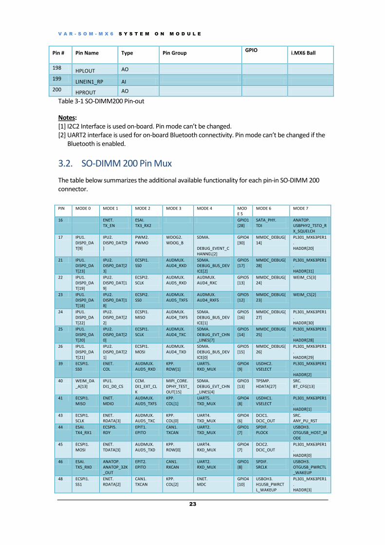
Table 3-1 SO-DIMM200 Pin-out
Notes: [1] I2C2 Interface is used on-board. Pin mode can’t be changed. [2] UART2 interface is used for on-board Bluetooth connectivity. Pin mode can’t be changed if the
Bluetooth is enabled.
3.2. SO-DIMM 200 Pin Mux
The table below summarizes the additional available functionality for each pin-in SO-DIMM 200 connector.
PIN MODE 0 MODE 1 MODE 2 MODE 3 MODE 4 MODE 5
MODE 6 MODE 7
16 ENET. TX_EN
ESAI. TX3_RX2
GPIO1[28]
SATA_PHY. TDI
ANATOP. USBPHY2_TSTO_RX_SQUELCH
17 IPU1. DISP0_DAT[9]
IPU2. DISP0_DAT[9]
PWM2. PWMO
WDOG2. WDOG_B
SDMA. DEBUG_EVENT_CHANNEL[2]
GPIO4[30]
MMDC_DEBUG[14]
PL301_MX63PER1. HADDR[20]
21 IPU1. DISP0_DAT[23]
IPU2. DISP0_DAT[23]
ECSPI1. SS0
AUDMUX. AUD4_RXD
SDMA. DEBUG_BUS_DEVICE[2]
GPIO5[17]
MMDC_DEBUG[28]
PL301_MX63PER1. HADDR[31]
22 IPU1. DISP0_DAT[19]
IPU2. DISP0_DAT[19]
ECSPI2. SCLK
AUDMUX. AUD5_RXD
AUDMUX. AUD4_RXC
GPIO5[13]
MMDC_DEBUG[24]
WEIM_CS[3]
23 IPU1. DISP0_DAT[18]
IPU2. DISP0_DAT[18]
ECSPI2. SS0
AUDMUX. AUD5_TXFS
AUDMUX. AUD4_RXFS
GPIO5[12]
MMDC_DEBUG[23]
WEIM_CS[2]
24 IPU1. DISP0_DAT[22]
IPU2. DISP0_DAT[22]
ECSPI1. MISO
AUDMUX. AUD4_TXFS
SDMA. DEBUG_BUS_DEVICE[1]
GPIO5[16]
MMDC_DEBUG[27]
PL301_MX63PER1. HADDR[30]
25 IPU1. DISP0_DAT[20]
IPU2. DISP0_DAT[20]
ECSPI1. SCLK
AUDMUX. AUD4_TXC
SDMA. DEBUG_EVT_CHN_LINES[7]
GPIO5[14]
MMDC_DEBUG[25]
PL301_MX63PER1. HADDR[28]
26 IPU1. DISP0_DAT[21]
IPU2. DISP0_DAT[21]
ECSPI1. MOSI
AUDMUX. AUD4_TXD
SDMA. DEBUG_BUS_DEVICE[0]
GPIO5[15]
MMDC_DEBUG[26]
PL301_MX63PER1. HADDR[29]
39 ECSPI1. SS0
ENET. COL
AUDMUX. AUD5_RXD
KPP. ROW[1]
UART5. RXD_MUX
GPIO4[9]
USDHC2. VSELECT
PL301_MX63PER1. HADDR[2]
40 WEIM_DA_A[13]
IPU1. DI1_D0_CS
CCM. DI1_EXT_CLK
MIPI_CORE. DPHY_TEST_OUT[15]
SDMA. DEBUG_EVT_CHN_LINES[4]
GPIO3[13]
TPSMP. HDATA[27]
SRC. BT_CFG[13]
41 ECSPI1. MISO
ENET. MDIO
AUDMUX. AUD5_TXFS
KPP. COL[1]
UART5. TXD_MUX
GPIO4[8]
USDHC1. VSELECT
PL301_MX63PER1. HADDR[1]
43 ECSPI1. SCLK
ENET. RDATA[3]
AUDMUX. AUD5_TXC
KPP. COL[0]
UART4. TXD_MUX
GPIO4[6]
DCIC1. DCIC_OUT
SRC. ANY_PU_RST
44 ESAI. TX4_RX1
ECSPI5. RDY
EPIT1. EPITO
CAN1. TXCAN
UART2. TXD_MUX
GPIO1[7]
SPDIF. PLOCK
USBOH3. OTGUSB_HOST_MODE
45 ECSPI1. MOSI
ENET. TDATA[3]
AUDMUX. AUD5_TXD
KPP. ROW[0]
UART4. RXD_MUX
GPIO4[7]
DCIC2. DCIC_OUT
PL301_MX63PER1. HADDR[0]
46 ESAI. TX5_RX0
ANATOP. ANATOP_32K_OUT
EPIT2. EPITO
CAN1. RXCAN
UART2. RXD_MUX
GPIO1[8]
SPDIF. SRCLK
USBOH3. OTGUSB_PWRCTL_WAKEUP
48 ECSPI1. SS1
ENET. RDATA[2]
CAN1. TXCAN
KPP. COL[2]
ENET. MDC
GPIO4[10]
USBOH3. H1USB_PWRCTL_WAKEUP
PL301_MX63PER1. HADDR[3]
V A R - S O M - M X 6 S Y S T E M O N M O D U L E
24
PIN MODE 0 MODE 1 MODE 2 MODE 3 MODE 4 MODE 5
MODE 6 MODE 7
50 WEIM_D[28]
I2C1. SDA
ECSPI4. MOSI
IPU2. CSI1_D[12]
UART2. CTS
GPIO3[28]
IPU1. EXT_TRIG
IPU1. DI0_PIN13
51 WEIM_D[29]
IPU1. DI1_PIN15
ECSPI4. SS0
UART2. RTS
GPIO3[29]
IPU2. CSI1_VSYNC
IPU1. DI0_PIN14
52 WEIM_D[24]
ECSPI4. SS2
UART3. TXD_MUX
ECSPI1. SS2
ECSPI2. SS2
GPIO3[24]
AUDMUX. AUD5_RXFS
UART1. DTR
53 WEIM_D[27]
IPU1. DI1_PIN13
IPU1. CSI0_D[0]
IPU2. CSI1_D[13]
UART2. RXD_MUX
GPIO3[27]
IPU1. SISG[3]
IPU1. DISP1_DAT[23]
54 WEIM_D[25]
ECSPI4. SS3
UART3. RXD_MUX
ECSPI1. SS3
ECSPI2. SS3
GPIO3[25]
AUDMUX. AUD5_RXC
UART1. DSR
55 WEIM_D[23]
IPU1. DI0_D0_CS
UART3. CTS
UART1. DCD
IPU2. CSI1_DATA_EN
GPIO3[23]
IPU1. DI1_PIN2
IPU1. DI1_PIN14
56 WEIM_EB[2]
ECSPI1. SS0
CCM. DI1_EXT_CLK
IPU2. CSI1_D[19]
HDMI_TX. DDC_SCL
GPIO2[30]
I2C2. SCL
SRC. BT_CFG[30]
57 WEIM_EB[3]
ECSPI4. RDY
UART3. RTS
UART1. RI
IPU2. CSI1_HSYNC
GPIO2[31]
IPU1. DI1_PIN3
SRC. BT_CFG[31]
61 USDHC2. DAT2
ECSPI5. SS1
WEIM_CS[3] AUDMUX. AUD4_TXD
KPP. ROW[6]
GPIO1[13]
CCM. STOP
ANATOP_TESTO[1]
62 USDHC2. DAT0
ECSPI5. MISO
AUDMUX. AUD4_RXD
KPP. ROW[7]
GPIO1[15]
DCIC2. DCIC_OUT
ANATOP_TESTO[2]
63 USDHC2. DAT1
ECSPI5. SS0
WEIM_CS[2] AUDMUX. AUD4_TXFS
KPP. COL[7]
GPIO1[14]
CCM. WAIT
ANATOP_TESTO[0]
64 USDHC2. CMD
ECSPI5. MOSI
KPP. ROW[5]
AUDMUX. AUD4_RXC
PCIE_CTRL. DIAG_STATUS_BUS_MUX[10]
GPIO1[11]
65 USDHC2. DAT3
ECSPI5. SS3
KPP. COL[6]
AUDMUX. AUD4_TXC
PCIE_CTRL. DIAG_STATUS_BUS_MUX[11]
GPIO1[12]
SJC. DONE
ANATOP_TESTO[3]
68 USDHC1. DAT0
ECSPI5. MISO
CAAM_WRAPPER. RNG_OSC_OBS
GPT. CAPIN1
PCIE_CTRL. DIAG_STATUS_BUS_MUX[8]
GPIO1[16]
HDMI_TX. OPHYDTB[1]
ANATOP_TESTO[7]
69 USDHC1. CMD
ECSPI5. MOSI
PWM4. PWMO
GPT. CMPOUT1
GPIO1[18]
ANATOP_TESTO[5]
70 USDHC1. DAT2
ECSPI5. SS1
GPT. CMPOUT2
PWM2. PWMO
WDOG1. WDOG_B
GPIO1[19]
WDOG1. WDOG_RST_B_DEB
ANATOP_TESTO[4]
71 USDHC1. DAT1
ECSPI5. SS0
PWM3. PWMO
GPT. CAPIN2
PCIE_CTRL. DIAG_STATUS_BUS_MUX[7]
GPIO1[17]
HDMI_TX. OPHYDTB[0]
ANATOP_TESTO[8]
73 USDHC1. DAT3
ECSPI5. SS2
GPT. CMPOUT3
PWM1. PWMO
WDOG2. WDOG_B
GPIO1[21]
WDOG2. WDOG_RST_B_DEB
ANATOP_TESTO[6]
75 WEIM_D[21]
ECSPI4. SCLK
IPU1. DI0_PIN17
IPU2. CSI1_D[11]
USBOH3. USBOTG_OC
GPIO3[21]
I2C1. SCL
SPDIF. IN1
77 WEIM_D[22]
ECSPI4. MISO
IPU1. DI0_PIN1
IPU2. CSI1_D[10]
USBOH3. USBOTG_PWR
GPIO3[22]
SPDIF. OUT1
PL301_MX63PER1. HWRITE
79 WEIM_D[30]
IPU1. DISP1_DAT[21]
IPU1. DI0_PIN11
IPU1. CSI0_D[3]
UART3. CTS
GPIO3[30]
USBOH3. USBH1_OC
PL301_MX63PER1. HPROT[0]
80 CAN2. TXCAN
IPU1. SISG[4]
USBOH3. USBOTG_OC
KPP. COL[4]
UART5. RTS
GPIO4[14]
MMDC_DEBUG[49]
PL301_MX63PER1. HADDR[7]
81 IPU1. CSI0_HSYNC
PCIE_CTRL. DIAG_STATUS_BUS_MUX[13]
CCM. CLKO
SDMA. DEBUG_PC[1]
GPIO5[19]
MMDC_DEBUG[30]
CHEETAH. TRCTL
82 CAN2. RXCAN
IPU1. SISG[5]
USBOH3. USBOTG_PWR
KPP. ROW[4]
UART5. CTS
GPIO4[15]
MMDC_DEBUG[50]
PL301_MX63PER1. HADDR[8]
83 IPU1. CSI0_D[11]
AUDMUX. AUD3_RXFS
ECSPI2. SS0
UART1. RXD_MUX
SDMA. DEBUG_PC[5]
GPIO5[29]
MMDC_DEBUG[34]
CHEETAH. TRACE[8]
84 WEIM_D[20]
ECSPI4. SS0
IPU1. DI0_PIN16
IPU2. CSI1_D[15]
UART1. RTS
GPIO3[20]
EPIT2. EPITO
85 IPU1. CSI0_D[10]
AUDMUX. AUD3_RXC
ECSPI2. MISO
UART1. TXD_MUX
SDMA. DEBUG_PC[4]
GPIO5[28]
MMDC_DEBUG[33]
CHEETAH. TRACE[7]
86 WEIM_D[19]
ECSPI1. SS1
IPU1. DI0_PIN8
IPU2. CSI1_D[16]
UART1. CTS
GPIO3[19]
EPIT1. EPITO
PL301_MX63PER1. HRESP
87 IPU1. CSI0_D[8]
WEIM_D[6] ECSPI2. SCLK
KPP. COL[7]
I2C1. SDA
GPIO5[26]
MMDC_DEBUG[47]
CHEETAH. TRACE[5]
88 IPU1. CSI0_D[9]
WEIM_D[7] ECSPI2. MOSI
KPP. ROW[7]
I2C1. SCL
GPIO5[27]
MMDC_DEBUG[48]
CHEETAH. TRACE[6]
V A R - S O M - M X 6 S Y S T E M O N M O D U L E
25
PIN MODE 0 MODE 1 MODE 2 MODE 3 MODE 4 MODE 5
MODE 6 MODE 7
90 ESAI. TX3_RX2
ENET. 1588_EVENT2_IN
ENET. ANATOP_ETHERNET_REF_OUT
USDHC1. LCTL
SPDIF. IN1
GPIO7[11]
I2C3. SDA
SJC. DE_B
92 ESAI. TX2_RX3
OBSERVE_MUX. OBSRV_INT_OUT4
KPP. ROW[7]
CCM. CLKO
CSU. CSU_ALARM_AUT[2]
GPIO1[5]
I2C3. SCL
CHEETAH. EVENTI
94 ANATOP. USBOTG_ID
ENET. RX_ER
ESAI. HCKR
SPDIF. IN1
ENET. 1588_EVENT2_OUT
GPIO1[24]
PHY. TDI
ANATOP. USBPHY1_TSTO_RX_HS_RXD
96 IPU1. CSI0_D[19]
WEIM_D[15] PCIE_CTRL. DIAG_STATUS_BUS_MUX[23]
UART5. CTS
SDMA. DEBUG_PC[13]
GPIO6[5]
MMDC_DEBUG[42]
ANATOP_TESTO[9]
113 IPU1. CSI0_D[18]
WEIM_D[14] PCIE_CTRL. DIAG_STATUS_BUS_MUX[22]
UART5. RTS
SDMA. DEBUG_PC[12]
GPIO6[4]
MMDC_DEBUG[41]
CHEETAH. TRACE[15]
115 IPU1. CSI0_D[15]
WEIM_D[11] PCIE_CTRL. DIAG_STATUS_BUS_MUX[19]
UART5. RXD_MUX
SDMA. DEBUG_PC[9]
GPIO6[1]
MMDC_DEBUG[38]
CHEETAH. TRACE[12]
117 IPU1. CSI0_D[17]
WEIM_D[13] PCIE_CTRL. DIAG_STATUS_BUS_MUX[21]
UART4. CTS
SDMA. DEBUG_PC[11]
GPIO6[3]
MMDC_DEBUG[40]
CHEETAH. TRACE[14]
120 IPU1. CSI0_VSYNC
WEIM_D[1] PCIE_CTRL. DIAG_STATUS_BUS_MUX[15]
SDMA. DEBUG_PC[3]
GPIO5[21]
MMDC_DEBUG[32]
CHEETAH. TRACE[0]
122 IPU1. CSI0_DATA_EN
WEIM_D[0] PCIE_CTRL. DIAG_STATUS_BUS_MUX[14]
SDMA. DEBUG_PC[2]
GPIO5[20]
MMDC_DEBUG[31]
CHEETAH. TRCLK
124 IPU1. CSI0_D[12]
WEIM_D[8] PCIE_CTRL. DIAG_STATUS_BUS_MUX[16]
UART4. TXD_MUX
SDMA. DEBUG_PC[6]
GPIO5[30]
MMDC_DEBUG[35]
CHEETAH. TRACE[9]
171 IPU1. CSI0_D[14]
WEIM_D[10] PCIE_CTRL. DIAG_STATUS_BUS_MUX[18]
UART5. TXD_MUX
SDMA. DEBUG_PC[8]
GPIO6[0]
MMDC_DEBUG[37]
CHEETAH. TRACE[11]
173 IPU1. CSI0_D[16]
WEIM_D[12] PCIE_CTRL. DIAG_STATUS_BUS_MUX[20]
UART4. RTS
SDMA. DEBUG_PC[10]
GPIO6[2]
MMDC_DEBUG[39]
CHEETAH. TRACE[13]
175 IPU1. CSI0_D[13]
WEIM_D[9] PCIE_CTRL. DIAG_STATUS_BUS_MUX[17]
UART4. RXD_MUX
SDMA. DEBUG_PC[7]
GPIO5[31]
MMDC_DEBUG[36]
CHEETAH. TRACE[10]
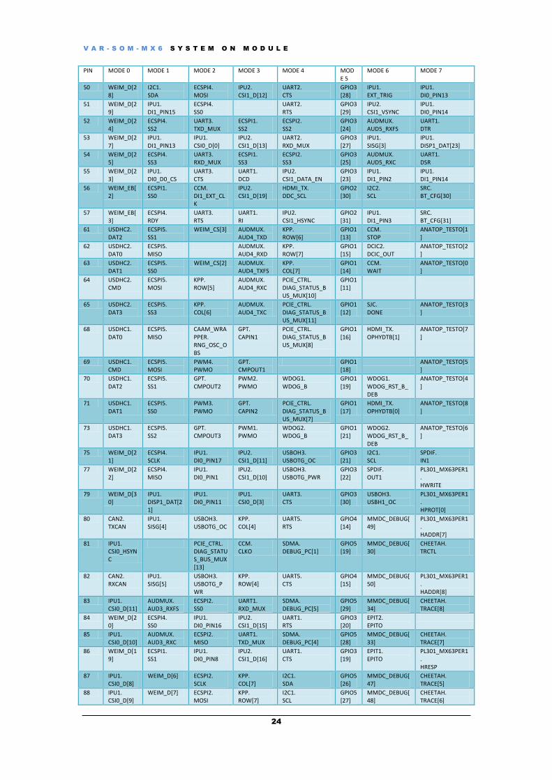
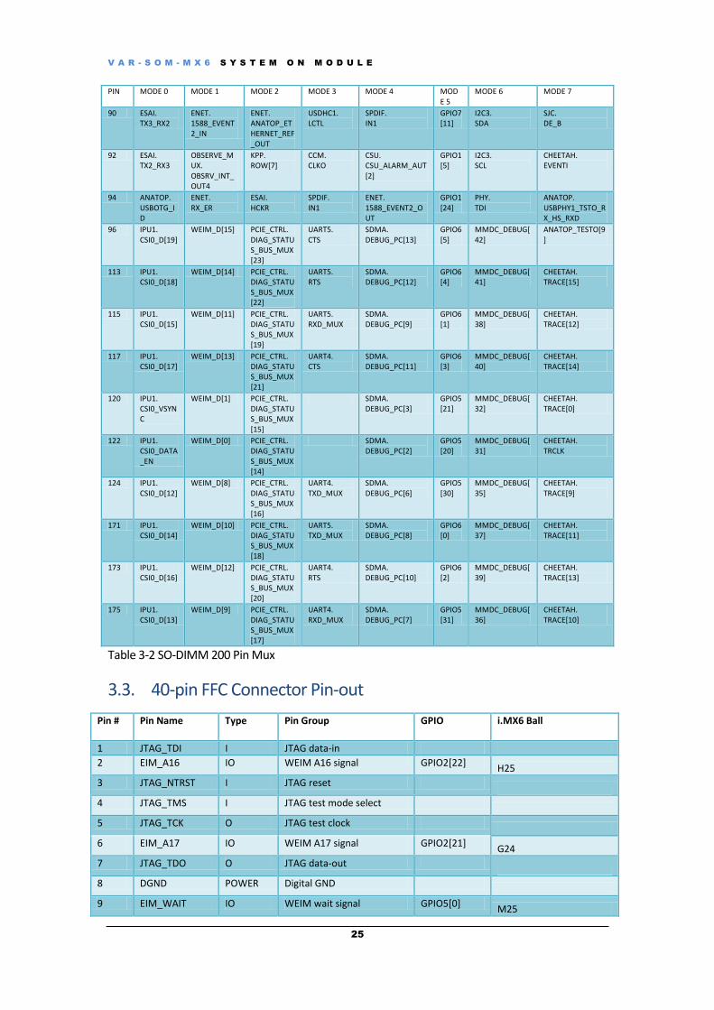
Table 3-2 SO-DIMM 200 Pin Mux
3.3. 40-pin FFC Connector Pin-out
Pin #
Pin Name
Type
Pin Group
GPIO i.MX6 Ball
1 JTAG_TDI I JTAG data-in
2 EIM_A16 IO WEIM A16 signal GPIO2[22] H25
3 JTAG_NTRST I JTAG reset
4 JTAG_TMS I JTAG test mode select
5 JTAG_TCK O JTAG test clock
6 EIM_A17 IO WEIM A17 signal GPIO2[21] G24
7 JTAG_TDO O JTAG data-out
8 DGND POWER Digital GND
9 EIM_WAIT IO WEIM wait signal GPIO5[0] M25
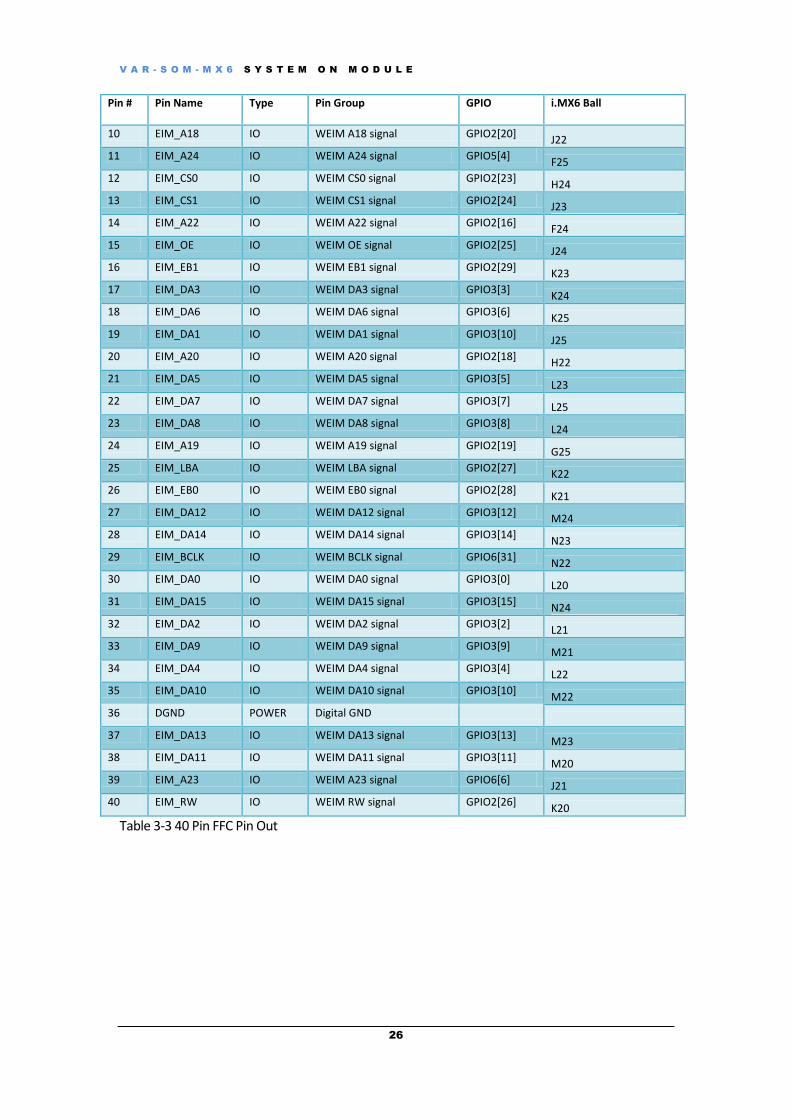
V A R - S O M - M X 6 S Y S T E M O N M O D U L E
26
Pin #
Pin Name
Type
Pin Group
GPIO i.MX6 Ball
10 EIM_A18 IO WEIM A18 signal GPIO2[20] J22
11 EIM_A24 IO WEIM A24 signal GPIO5[4] F25
12 EIM_CS0 IO WEIM CS0 signal GPIO2[23] H24
13 EIM_CS1 IO WEIM CS1 signal GPIO2[24] J23
14 EIM_A22 IO WEIM A22 signal GPIO2[16] F24
15 EIM_OE IO WEIM OE signal GPIO2[25] J24
16 EIM_EB1 IO WEIM EB1 signal GPIO2[29] K23
17 EIM_DA3 IO WEIM DA3 signal GPIO3[3] K24
18 EIM_DA6 IO WEIM DA6 signal GPIO3[6] K25
19 EIM_DA1 IO WEIM DA1 signal GPIO3[10] J25
20 EIM_A20 IO WEIM A20 signal GPIO2[18] H22
21 EIM_DA5 IO WEIM DA5 signal GPIO3[5] L23
22 EIM_DA7 IO WEIM DA7 signal GPIO3[7] L25
23 EIM_DA8 IO WEIM DA8 signal GPIO3[8] L24
24 EIM_A19 IO WEIM A19 signal GPIO2[19] G25
25 EIM_LBA IO WEIM LBA signal GPIO2[27] K22
26 EIM_EB0 IO WEIM EB0 signal GPIO2[28] K21
27 EIM_DA12 IO WEIM DA12 signal GPIO3[12] M24
28 EIM_DA14 IO WEIM DA14 signal GPIO3[14] N23
29 EIM_BCLK IO WEIM BCLK signal GPIO6[31] N22
30 EIM_DA0 IO WEIM DA0 signal GPIO3[0] L20
31 EIM_DA15 IO WEIM DA15 signal GPIO3[15] N24
32 EIM_DA2 IO WEIM DA2 signal GPIO3[2] L21
33 EIM_DA9 IO WEIM DA9 signal GPIO3[9] M21
34 EIM_DA4 IO WEIM DA4 signal GPIO3[4] L22
35 EIM_DA10 IO WEIM DA10 signal GPIO3[10] M22
36 DGND POWER Digital GND
37 EIM_DA13 IO WEIM DA13 signal GPIO3[13] M23
38 EIM_DA11 IO WEIM DA11 signal GPIO3[11] M20
39 EIM_A23 IO WEIM A23 signal GPIO6[6] J21
40 EIM_RW IO WEIM RW signal GPIO2[26] K20
Table 3-3 40 Pin FFC Pin Out

V A R - S O M - M X 6 V 1 . 0 S Y S T E M O N M O D U L E
3.4. 40-pin FFC Mux
The table below summarizes the additional available functionality for each pin in the 40pin FFC connector.
PIN MODE 0 MODE 1 MODE 2 MODE 3 MODE 4 MODE 5 MODE 6 MODE 7
1 JTAG_TDI
2 WEIM_A[16]
IPU1. DI1_DISP_CLK
IPU2. CSI1_PIXCLK
MIPI_CORE. DPHY_TEST_OUT[23]
GPIO2[22] TPSMP. HDATA[6]
SRC. BT_CFG[16]
3 JTAG_NTRST
4 JTAG_TMS
5 JTAG_TCK
6 WEIM_A[17]
IPU1. DISP1_DAT[12]
IPU2. CSI1_D[12]
MIPI_CORE. DPHY_TEST_OUT[22]
GPIO2[21] TPSMP. HDATA[5]
SRC. BT_CFG[17]
7 JTAG_TDO
9 WEIM_WAIT
WEIM_DTACK_B
GPIO5[0] TPSMP. HDATA[30]
SRC. BT_CFG[25]
10 WEIM_A[18]
IPU1. DISP1_DAT[13]
IPU2. CSI1_D[13]
MIPI_CORE. DPHY_TEST_OUT[21]
GPIO2[20] TPSMP. HDATA[4]
SRC. BT_CFG[18]
11 WEIM_A[24]
IPU1. DISP1_DAT[19]
IPU2. CSI1_D[19]
IPU2. SISG[2]
IPU1. SISG[2]
GPIO5[4] PL301_MX6Q_PER1. HPROT[2]
SRC. BT_CFG[24] EIM_
12 WEIM_CS[0]
IPU1. DI1_PIN5
ECSPI2. SCLK
MIPI_CORE. DPHY_TEST_OUT[24]
GPIO2[23] TPSMP. HDATA[7]
13 WEIM_CS[1]
IPU1. DI1_PIN6
ECSPI2. MOSI
MIPI_CORE. DPHY_TEST_OUT[25]
GPIO2[24] TPSMP. HDATA[8]
14 WEIM_A[22]
IPU1. DISP1_DAT[17]
IPU2. CSI1_D[17]
GPIO2[16] TPSMP. HDATA[0]
SRC. BT_CFG[22]
15 WEIM_OE IPU1. DI1_PIN7
ECSPI2. MISO
MIPI_CORE. DPHY_TEST_OUT[26]
GPIO2[25] TPSMP. HDATA[9]
16 WEIM_EB[1]
IPU1. DISP1_DAT[10]
IPU2. CSI1_D[10]
MIPI_CORE. DPHY_TEST_OUT[1]
GPIO2[29] TPSMP. HDATA[13]
SRC. BT_CFG[28]
17 WEIM_DA_A[3]
IPU1. DISP1_DAT[6]
IPU2. CSI1_D[6]
MIPI_CORE. DPHY_TEST_OUT[5]
ANATOP. USBPHY1_TSTI_TX_HIZ
GPIO3[3] TPSMP. HDATA[17]
SRC. BT_CFG[3]
18 WEIM_DA_A[6]
IPU1. DISP1_DAT[3]
IPU2. CSI1_D[3]
MIPI_CORE. DPHY_TEST_OUT[8]
ANATOP. USBPHY1_TSTI_TX_DN
GPIO3[6] TPSMP. HDATA[20]
SRC. BT_CFG[6]
19 WEIM_DA_A[10]
IPU1. DI1_PIN15
IPU2. CSI1_DATA_EN
MIPI_CORE. DPHY_TEST_OUT[12]
GPIO3[10] TPSMP. HDATA[24]
SRC. BT_CFG[10]
20 WEIM_A[20]
IPU1. DISP1_DAT[15]
IPU2. CSI1_D[15]
MIPI_CORE. DPHY_TEST_OUT[19]
GPIO2[18] TPSMP. HDATA[2]
SRC. BT_CFG[20]
21 WEIM_DA_A[5]
IPU1. DISP1_DAT[4]
IPU2. CSI1_D[4]
MIPI_CORE. DPHY_TEST_OUT[7]
ANATOP. USBPHY1_TSTI_TX_DP
GPIO3[5] TPSMP. HDATA[19]
SRC. BT_CFG[5]
22 WEIM_DA_A[7]
IPU1. DISP1_DAT[2]
IPU2. CSI1_D[2]
MIPI_CORE. DPHY_TEST_OUT[9]
GPIO3[7]
TPSMP. HDATA[21]
SRC. BT_CFG[7]
23 WEIM_DA_A[8]
IPU1. DISP1_DAT[1]
IPU2. CSI1_D[1]
MIPI_CORE. DPHY_TEST_OUT[10]
GPIO3[8] TPSMP. HDATA[22]
SRC. BT_CFG[8]
24 WEIM_A[19]
IPU1. DISP1_DAT[14]
IPU2. CSI1_D[14]
MIPI_CORE. DPHY_TEST_OUT[20]
GPIO2[19] TPSMP. HDATA[3]
SRC. BT_CFG[19]

V A R - S O M - M X 6 S Y S T E M O N M O D U L E
28
PIN MODE 0 MODE 1 MODE 2 MODE 3 MODE 4 MODE 5 MODE 6 MODE 7
25 WEIM_LBA
IPU1. DI1_PIN17
ECSPI2. SS1
GPIO2[27] TPSMP. HDATA[11]
SRC. BT_CFG[26]
26 WEIM_EB[0]
IPU1. DISP1_DAT[11]
IPU2. CSI1_D[11]
MIPI_CORE. DPHY_TEST_OUT[0]
CCM. PMIC_RDY
GPIO2[28] TPSMP. HDATA[12]
SRC. BT_CFG[27]
27 WEIM_DA_A[12]
IPU1. DI1_PIN3
IPU2. CSI1_VSYNC
MIPI_CORE. DPHY_TEST_OUT[14]
SDMA. DEBUG_EVT_CHN_LINES[3]
GPIO3[12] TPSMP. HDATA[26]
SRC. BT_CFG[12]
28 WEIM_DA_A[14]
IPU1. DI1_D1_CS
CCM. DI0_EXT_CLK
MIPI_CORE. DPHY_TEST_OUT[16]
SDMA. DEBUG_EVT_CHN_LINES[5]
GPIO3[14] TPSMP. HDATA[28]
TPSMP. HDATA[28]
29 WEIM_BCLK
IPU1. DI1_PIN16
GPIO6[31] TPSMP. HDATA[31]
30 WEIM_DA_A[0]
IPU1. DISP1_DAT[9]
IPU2. CSI1_D[9]
MIPI_CORE. DPHY_TEST_OUT[2]
GPIO3[0] TPSMP. HDATA[14]
SRC. BT_CFG[0]
31 WEIM_DA_A[15]
IPU1. DI1_PIN1
IPU1. DI1_PIN4
MIPI_CORE. DPHY_TEST_OUT[17]
GPIO3[15] TPSMP. HDATA[29]
SRC. BT_CFG[15]
32 WEIM_DA_A[2]
IPU1. DISP1_DAT[7]
IPU2. CSI1_D[7]
MIPI_CORE. DPHY_TEST_OUT[4]
ANATOP. USBPHY1_TSTI_TX_HS_MODE
GPIO3[2] TPSMP. HDATA[16]
SRC. BT_CFG[2]
33 WEIM_DA_A[9]
IPU1. DISP1_DAT[0]
IPU2. CSI1_D[0]
MIPI_CORE. DPHY_TEST_OUT[11]
GPIO3[9] TPSMP. HDATA[23]
SRC. BT_CFG[9]
34 WEIM_DA_A[4]
IPU1. DISP1_DAT[5]
IPU2. CSI1_D[5]
MIPI_CORE. DPHY_TEST_OUT[6
ANATOP. USBPHY1_TSTI_TX_EN
GPIO3[4] TPSMP. HDATA[18]
SRC. BT_CFG[4]
35 WEIM_DA_A[10]
IPU1. DI1_PIN15
IPU2. CSI1_DATA_EN
MIPI_CORE. DPHY_TEST_OUT[12]
GPIO3[10] TPSMP. HDATA[24]
SRC. BT_CFG[10]
37 WEIM_DA_A[13]
IPU1. DI1_D0_CS
CCM. DI1_EXT_CLK
MIPI_CORE. DPHY_TEST_OUT[15]
SDMA. DEBUG_EVT_CHN_LINES[4]
GPIO3[13] TPSMP. HDATA[27]
SRC. BT_CFG[13]
38 WEIM_DA_A[11]
IPU1. DI1_PIN2
IPU2. CSI1_HSYNC
MIPI_CORE. DPHY_TEST_OUT[13]
SDMA. DEBUG_EVT_CHN_LINES[6]
GPIO3[11]
TPSMP. HDATA[25]
SRC. BT_CFG[11]
39 WEIM_A[23]
IPU1. DISP1_DAT[18]
IPU2. CSI1_D[18]
IPU2. SISG[3]
IPU1. SISG[3]
GPIO6[6] PL301_MX6Q_ PER1 HPROT[3]
SRC. BT_CFG[23]
40 WEIM_RW
IPU1. DI1_PIN8
ECSPI2. SS0
MIPI_CORE. DPHY_TEST_OUT[27]
GPIO2[26] TPSMP. HDATA[10]
SRC. BT_CFG[29]
Table 3-4 40-pin FFC Mux Interface Details
3.5. Overview
This chapter describes in detail the VAR-SOM-MX6 interfaces, referring to the default SoM pin names. However, many additional interfaces are available when different pin modes are
V A R - S O M - M X 6 S Y S T E M O N M O D U L E
29
selected by the user. Tables 3-2 and 3-4 (SO-DIMM200 /40-PIN FPC Pin Mux) detail the additional possible options for each pin on the VAR-SOM-MX6 connectors. The following list describes this chapter’s column header tables: Signal: VAR-SOM-MX6 original pin name Pin#: Pin number on the SO-DIMM200 connector (excluding GPMC & JTAG interfaces which are exposed by the 40-pin FCC connector) Type: Pin type & direction:
I – In
O – Out
DS – Differential Signal
A – Analog
Power – Power Pin
Description: Short pin functionality description
3.6. Display Interfaces
3.6.1. Overview
The VAR-SOM-MX6 video graphics subsystem consists of the following dedicated modules:
• Video Processing Unit (VPU): A multi-standard high performance video/image CODEC
• Three Graphics Processing Units (GPUs):
• 3D GPU: Accelerating the generation of 3D graphics (OpenGL/ES)
• 2D GPU: Accelerating the generation of 2D graphics (BitBLT)
• OpenVG: Accelerating vector graphics (OpenVG)
• Two (identical) Image Processing Units (IPUs): Providing connectivity to cameras and
displays, related processing, synchronization and control
• Display interface bridges: Providing optional translation from the digital display interface
supported by the IPU to other interfaces:
• LVDS bridge (LDB): providing up to two LVDS interfaces
• HDMI transmitter
• MIPI/DSI transmitter
• MIPI/CSI-2 receiver
• Two (identical) Display Content Integrity Checkers (DCIC) are used to authenticate
sensitive displayed data
• Video Data Order Adapter (VDOA): Applied to re-order video data from the "tiled" order
used by the VPU to the conventional raster-scan order needed by the IPU
V A R - S O M - M X 6 S Y S T E M O N M O D U L E
30
3.6.2. Interfaces
• Two LVDS channels, driven by the LDB; pixel clock up to 170 MHz
• One HDMI port (ver. 1.4) - driven by the HDMI transmitter: Pixel clock up to 266
MHz (gated by the IPU capabilities)
• One MIPI/DSI port - driven by the MIPI/DSI transmitter; two data lanes @ 1 GHz
• Each IPU has two display ports. Up to four external ports can be active at any given
time (additional asynchronous data flows can be sent though the parallel ports and
the MIPI/DSI port).
• Read access is supported as follows:
- For the Parallel0 port: through DI00
- For the Parallel1 port: through DI10
- For the MIPI/DSI port: through DI01 or DI11
• Inputs to either of the DCIC's are taken from one of the following buses
- For each of the parallel interfaces: Probing the I/O loopback (essentially
equivalent to probing the external wires).
- For other integrated interfaces (e.g. LVDS), probing the DI1 output of each of
the IPUs (essentially equivalent to the inputs of the serializes)
- For the data enable signal two control signals are probed from each of the
above buses
3.6.2.1. DSI
VAR-SOM-MX6 MIPI DSI Host Controller supports the following features: Compliant with MIPI Alliance Specification for Display Serial Interface (DSI), Version 1.01.00 - 21 February 2008: • Fully compliant with MIPI Alliance standard for Display Pixel Interface (DPI-2),Version
2.00 15th September, 2005 with Pixel Data bus width of up to 24-bits
• Compliant with MIPI Alliance standard for Display Bus Interface (DBI-2) Version 2.00 29th
November, 2005. Supported DBI types are:
- Type B
- 16-bit, 9-bit and 8-bit data bus width
• DBI and DPI interface can coexist but only one is operational
• Support all commands defined in the MIPI Alliance Specification for Display Command
Set (DCS), version 1.02.00 23rd July, 2009
Interface with MIPI D-PHY following PHY Protocol Interface (PPI), as defined in MIPI Alliance Specification for D-PHY, version 1.00.00 14th May, 2009. Supports up to 2 D-PHY data lanes: • Bidirectional communication and escape mode support through the data lane
• Programmable display resolutions, from 160 x 120(QQVGA) to
1024 x 768(XVGA)
• Multiple peripheral support capability, configurable virtual channels
• Video mode pixel formats, 16 bpp (5,6,5 RGB), 18 bpp (6,6,6,RGB) packed,
18 bpp (6,6,6,RGB) loosely, 24 bpp (8,8,8,RGB)
• Supports the transmission of all generic commands
• ECC and checksum capabilities
V A R - S O M - M X 6 S Y S T E M O N M O D U L E
31
• End of Transmission Packet (EoTp) support
• Supports ultra-low power mode
• Schemes for fault recovery
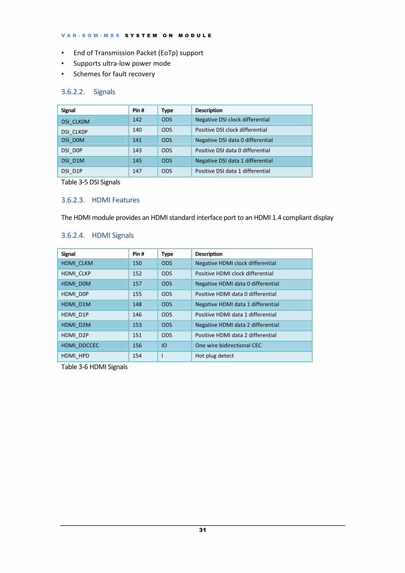
3.6.2.2. Signals
Signal Pin # Type Description
DSI_CLK0M 142 ODS Negative DSI clock differential
DSI_CLK0P 140 ODS Positive DSI clock differential
DSI_D0M 141 ODS Negative DSI data 0 differential
DSI_D0P 143 ODS Positive DSI data 0 differential
DSI_D1M 145 ODS Negative DSI data 1 differential
DSI_D1P 147 ODS Positive DSI data 1 differential
Table 3-5 DSI Signals
3.6.2.3. HDMI Features
The HDMI module provides an HDMI standard interface port to an HDMI 1.4 compliant display
3.6.2.4. HDMI Signals
Signal Pin # Type Description
HDMI_CLKM 150 ODS Negative HDMI clock differential
HDMI_CLKP 152 ODS Positive HDMI clock differential
HDMI_D0M 157 ODS Negative HDMI data 0 differential
HDMI_D0P 155 ODS Positive HDMI data 0 differential
HDMI_D1M 148 ODS Negative HDMI data 1 differential
HDMI_D1P 146 ODS Positive HDMI data 1 differential
HDMI_D2M 153 ODS Negative HDMI data 2 differential
HDMI_D2P 151 ODS Positive HDMI data 2 differential
HDMI_DDCCEC 156 IO One wire bidirectional CEC
HDMI_HPD 154 I Hot plug detect
Table 3-6 HDMI Signals
V A R - S O M - M X 6 S Y S T E M O N M O D U L E
32
3.6.2.5. LVDS Interface
LVDS Display Bridge (LDB) will be used to connect the IPU (Image Processing Unit) to the External LVDS display interface. Relevant Standards: 1. ANSI EIA-644-A. Electrical Characteristics of Low Voltage Differential Signaling (LVDS)
interface circuits.
2. SPWG notebook panel specification (V3.8 from 03/2007)
http://www.spwg.org/specifications.htm
3. PSWG standards (Panel Standardization Working Group) - set of standards for panels
using LVDS, all available from http://www.vesa.org
4. DISM standard JEIDA-59-1999
There are 2 LVDS channels. These outputs are used to communicate RGB data and controls to external LCD displays. The LVDS ports may be used as follows: • Single channel output
• Dual channel output (one input source, two channel outputs for two displays)
• Split channel output (one input source, split to two channels on output)
• Separate two channel output (two input sources from IPU)
The output LVDS port must comply with one.
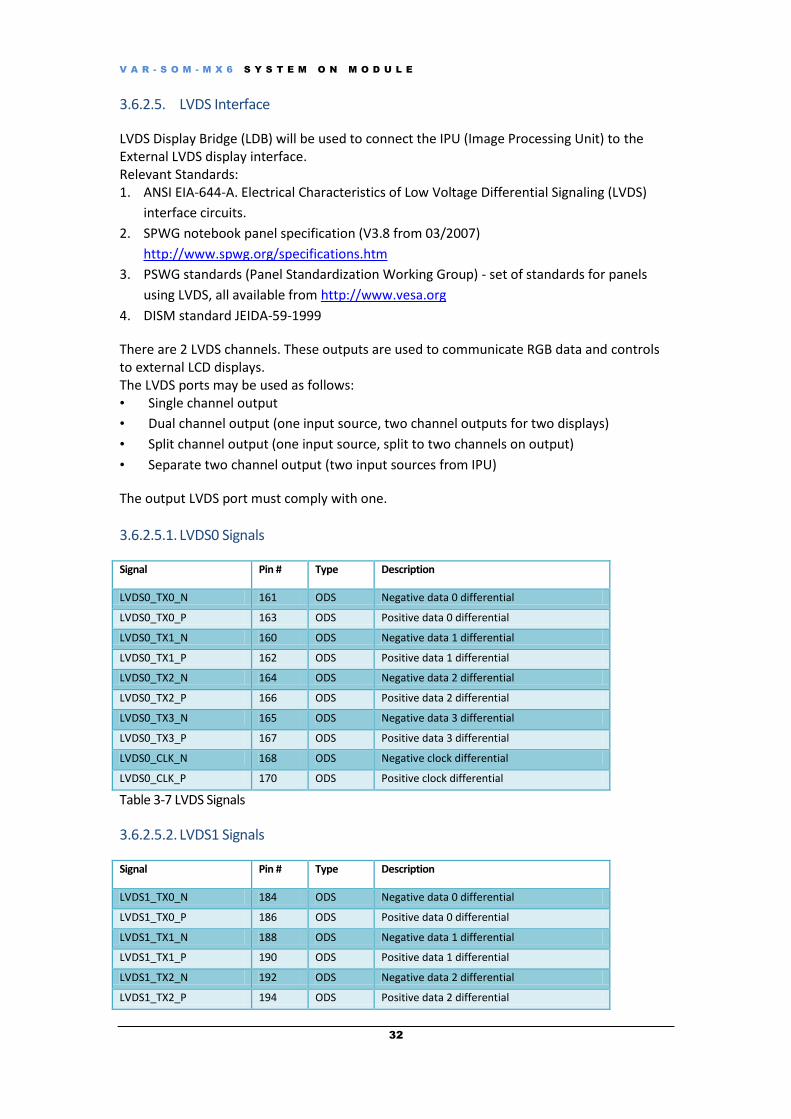
3.6.2.5.1. LVDS0 Signals
Signal Pin # Type Description
LVDS0_TX0_N 161 ODS Negative data 0 differential
LVDS0_TX0_P 163 ODS Positive data 0 differential
LVDS0_TX1_N 160 ODS Negative data 1 differential
LVDS0_TX1_P 162 ODS Positive data 1 differential
LVDS0_TX2_N 164 ODS Negative data 2 differential
LVDS0_TX2_P 166 ODS Positive data 2 differential
LVDS0_TX3_N 165 ODS Negative data 3 differential
LVDS0_TX3_P 167 ODS Positive data 3 differential
LVDS0_CLK_N 168 ODS Negative clock differential
LVDS0_CLK_P 170 ODS Positive clock differential
Table 3-7 LVDS Signals
3.6.2.5.2. LVDS1 Signals
Signal Pin # Type Description
LVDS1_TX0_N 184 ODS Negative data 0 differential
LVDS1_TX0_P 186 ODS Positive data 0 differential
LVDS1_TX1_N 188 ODS Negative data 1 differential
LVDS1_TX1_P 190 ODS Positive data 1 differential
LVDS1_TX2_N 192 ODS Negative data 2 differential
LVDS1_TX2_P 194 ODS Positive data 2 differential
V A R - S O M - M X 6 S Y S T E M O N M O D U L E
33
LVDS1_TX3_N 183 ODS Negative data 3 differential
LVDS1_TX3_P 181 ODS Positive data 3 differential
LVDS1_CLK_N 180 ODS Negative clock differential
LVDS1_CLK_P 182 ODS Positive clock differential
Table 3-8 LVDS Signals
3.7. Touch Screen
VAR-SOM-MX6 features a native, 4-wire resistive touch panel interface based on touch screen controller features
Compatible with 4-wire resistive touch screens
Pen-detection and nIRQ generation
Supports several schemes of measurement, averaging to filter noise
3.7.1. Touch-screen Controller Signals
Signal Pin # Type Description
TS_X- 187 AI Touch screen X minus
TS_Y- 193 AI Touch screen Y minus
TS_X+ 189 AI Touch screen X plus
TS_Y+ 191 AI Touch screen Y plus
Table 3-9 Touch-screen Signals
3.8. Camera Interfaces
3.8.1. MIPI CSI-2
The CSI-2 Host Controller is a digital core that implements all protocol functions defined in the MIPI CSI-2 specification, providing an interface between the system and the MIPI D-PHY, allowing communication with an MIPI CSI-2 compliant camera sensor.
The MIPI CSI-2 host controller supports the following features: • Compliance with MIPI Alliance standard for camera serial interface 2 (CSI-2), version 1.00
29th November, 2005
• Optional support for Camera Control Interface (CCI) through the use of DesignWare Core
(DW_apb_i2c)
• Interface with MIPI D-PHY following PHY Protocol Interface (PPI), as defined in MIPI
Alliance Specification for D-PHY, version 1.00.00 14th May, 2009
• Supports up to 4 D-PHY Rx data lanes
• Dynamically configurable multi-lane merging
• Long and short packet decoding
• Timing accurate signaling of frame and line synchronization packets
• Support for several frame formats such as:
- General frame or digital interlaced video with or without accurate sync timing

V A R - S O M - M X 6 S Y S T E M O N M O D U L E
34
- Data type (packet or frame level) and virtual channel interleaving
• 32-bit image data interface delivering data formatted as recommended in CSI-2
specification
• Supports all primary and secondary data formats:
- RGB, YUV and RAW color space definitions
- From 24-bit down to 6-bit per pixel
- Generic or user-defined byte-based data types
- Error detection and correction:
- PHY level
- Packet level
- Line level
- Frame level
3.8.1.1. Signals
Signal Pin # Type Description
CSI_CLK0M 137 IDS Negative CSI-2 clock differential
CSI_CLK0P 135 IDS Positive CSI-2 clock differential
CSI_D0M 121 IDS Negative CSI-2 data 0 differential
CSI_D0P 119 IDS Positive CSI-2 data 0 differential
CSI_D1M 123 IDS Negative CSI-2 data 1 differential
CSI_D1P 125 IDS Positive CSI-2 data 1 differential
CSI_D2M 129 IDS Negative CSI-2 data 2 differential
CSI_D2P 127 IDS Positive CSI-2 data 2 differential
CSI_D3M 131 IDS Negative CSI-2 data 3 differential
CSI_D3P 133 IDS Positive CSI-2 data 3 differential
Table 3-10 CSI-2 Signals
3.8.2. CSIx
Based on i.MX6 IPU, the VAR-SOM-MX6 supports two camera ports - each controlled by a CSI sub-block, providing a connection to image sensors and related devices.
3.8.3. CSI0 Signals
Signal Pin # Type Description
CSI0_DAT12 124 IO Camera data12 line
CSI0_DAT13 175 IO Camera data13 line
CSI0_DAT14 171 IO Camera data14 line
CSI0_DAT15 115 IO Camera data15 line
CSI0_DAT16 173 IO Camera data16 line
CSI0_DAT17 117 IO Camera data17 line
CSI0_DAT18 113 IO Camera data18 line
CSI0_DAT19 96 IO Camera data19 line
CSI0_DATA_EN 122 IO Camera data enable
CSI0_HSYNCH 81 IO Camera horizontal sync
V A R - S O M - M X 6 S Y S T E M O N M O D U L E
35
CSI0_PIXCLK 177 IO Camera pixel clock
CSI0_VSYNC 120 IO Camera vertical sync
Table 3-11 CSI0 Signals
3.8.4. CSI1 Signals
CSI1 Signals are exposed by the 40-pin FFC connector
Signal Pin # Type Description
CSI1_D[0] 33 IO Camera data 0 line
CSI1_D[1] 23 IO Camera data 1 line
CSI1_D[2] 16 IO Camera data 2 line
CSI1_D[3] 26 IO Camera data 3 line
CSI1_D[4] 6 IO Camera data 4 line
CSI1_D[5] 10 IO Camera data 5 line
CSI1_D[6] 24 IO Camera data 6 line
CSI1_D[7] 20 IO Camera data 7 line
CSI1_D[8] 39 IO Camera data 8 line
CSI1_D[9] 22 IO Camera data 9 line
CSI1_D[10] 18 IO Camera data 10 line
CSI1_D[11] 21 IO Camera data 11 line
CSI1_D[12] 34 IO Camera data 12 line
CSI1_D[13] 17 IO Camera data 13 line
CSI1_D[14] 32 IO Camera data 14 line
CSI1_D[15] 19 IO Camera data 15 line
CSI1_DATA_EN 35 IO Camera data enable
CSI1_HSYNC 38 IO Camera horizontal sync
CSI1_PIXCLK 2 IO Camera pixel clock
CSI1_VSYNC 27 IO Camera vertical sync
Table 3-12 CSI1 Signals

V A R - S O M - M X 6 S Y S T E M O N M O D U L E
36
3.9. Gigabit Ethernet
3.9.1. Gigabit Ethernet Features
The Ethernet Media Access Controller (MAC) is designed to support 10/100/1000 Mbps Ethernet/IEEE 802.3 networks. An external Gigabit magnetic is required to complete the interface to the media. The i.MX 6 Dual / Quad processors also consist of HW assist for IEEE1588 standard. See the IEEE1588 section for more details.
3.9.2. Gigabit Ethernet Magnetics
In order to utilize the VAR-SOM-MX6 Gigabit Ethernet interface, compatible magnetics should be used on the carrier board.
Vendor Part Number Package Cores Configuration
Pulse H5007NL Transformer 8 Auto-MDX
TDK TLA-7T101LF Transformer 8 Auto-MDX
Pulse J0G-0009NL Integrated RJ45 8 Auto-MDX
Table 3-13 Qualified Magnetics
3.9.3. Gigabit Ethernet Signals
Table 3-14 Gigabit Ethernet Signals
3.10. Wi-Fi & Bluetooth
The VAR-SOM-MX6 contains, LS Research TiWi-R2, a high performance 2.4 GHz IEEE 802.11 b/g/n Bluetooth 2.1+EDR radio module. The module is based on TI’s WL-1271 chipset. The module realizes the necessary PHY/MAC layers to support WLAN applications in conjunction with a host processor over a SDIO interface. The module also provides a Bluetooth platform through the HCI transport layer. Both WLAN and Bluetooth share the same antenna port.
IEEE 802.11 b/g/n
Bluetooth 2.1+EDR, Power Class 1.5.
U.FL connector for external antenna.
Integrated band-pass filter
3.11. USB Host 2.0
The USB controller block provides high performance USB functionality that conforms to the USB 2.0 specification.
Signal Pin # Type Description
MDI_A+ 3 DS Positive A differential lane
MDI_A- 5 DS Negative A differential lane
MDI_B+ 9 DS Positive B differential lane
MDI_B- 11 DS Negative B differential lane
MDI_C+ 4 DS Positive C differential lane
MDI_C- 6 DS Negative C differential lane
MDI_D+ 10 DS Positive D differential lane
MDI_D- 12 DS Negative D differential lane
V A R - S O M - M X 6 S Y S T E M O N M O D U L E
37
3.11.1. USB Host1 Signals
Signal Pin # Type Description
USB_HOST_DP 110 IODS Positive USB host data
USB_HOST_DN 108 IODS Negative USB host data
USB_H1_VBUS 104 I USB 2.0 VBUS indicator (5V)
USB_H1_OC 79 I USB host over current indicator
Table 3-15 USB Host1 Signals
3.12. USB 2.0 OTG
3.12.1. USB 2.0 On-the-go Features
High-speed OTG core • HS/FS/LS UTMI compliant interface
• High speed, full speed and low speed operation in host mode (with UTMI
transceiver)
• High speed, and full speed operation in peripheral mode (with UTMI transceiver)
• Hardware support for OTG signaling, session request protocol, and host negotiation
protocol
• Up to 8 bidirectional endpoints
• Integrated HS USB PHY
3.12.2. OTG Signals
Signal Pin # Type Description
USB_OTG_DN 114 IODS Negative USB OTG data
USB_OTG_DP 116 IODS Positive USB OTG data
USB_OTG_VBUS 106 I USB 2.0 OTG VBUS indicator (5V)
USB_OTG_ID 94 I USB OTG host/client ID Low : Host mode Float: Client mode
Table 3-16 USB OTG Signals
3.13. MMC/SD/SDIO
i.MX 6 Dual / Quad specific SoC characteristics: • Fully compliant with MMC command/response sets and physical layer as defined in the
Multimedia Card System specification v4.2/4.3/4.4, including high-capacity (size > 2 GB)
cards HC MMC.
• Fully compliant with SD command/response sets and physical layer as defined in the SD
Memory Card specifications v3.0, including high-capacity SDHC cards up to 32 GB
• Fully compliant with SDIO command/response sets and interrupt/read-wait mode as
defined in the SDIO Card specification, Part E1 v1.10
• Fully compliant with SD Card specification, Part A2, SD Host Controller Standard
specification v2.00
• 1-bit or 4-bit transfer mode specifications for SD and SDIO cards up to UHS-I SDR104
mode (104 MB/s max)
V A R - S O M - M X 6 S Y S T E M O N M O D U L E
38
• 1-bit, 4-bit, or 8-bit transfer mode specifications for MMC cards up to 52 MHz in both
SDR and DDR modes (104 MB/s max). However, the SoC level integration and I/O muxing
logic restrict functionality to the following:
3.13.1. SDMMC1 Signals
Table 3-17 SDMMC1 Signals
3.13.2. SDMMC2 Signals
Table 3-18 SDMMC2 Signals
3.14. Audio
The VAR-SOM-MX6 features three audio interfaces:
Audio codec - stereo line-in/out and digital microphone
Digital audio mux
S/PDIF in/out
3.14.1. Audio Features
3.14.1.1. Analog
Analog audio signals are featured by an on-board TLV320AIC3106 audio codec device. Please refer to the TLV320AIC3106 data sheet for detailed electrical characteristics of relevant
interfaces http://www.ti.com/product/tlv320aic3106.
3.14.1.2. Digital AUDMUX
Key features of the block include: • Two internal ports
• Four external ports
• Full 6-wire SSI interfaces for asynchronous receive and transmit
• Configurable 4-wire (synchronous) or 6-wire (asynchronous) peripheral interfaces
Signal Pin # Type Description
SD1_CLK 72 O Clock for MMC/SD/SDIO card
SD1_CMD 69 IO CMD line connect to card
SD1_DATA0 68 IO DAT0 line in all modes
Also used to detect busy state
SD1_DATA1 71 IO DAT1 line-in
SD1_DATA2 70 IO DAT2 line
SD1_DATA3 73 IO DAT3 line-in
Signal Pin # Type Description
SD2_CLK 60 O Clock for MMC/SD/SDIO card
SD2_CMD 64 IO CMD line connect to card
SD2_DATA0 62 IO DAT0 line in all modes
(also used to detect busy state)
SD2_DATA1 63 IO DAT1 line-in
SD2_DATA2 61 IO DAT2 line
SD2_DATA3 65 IO DAT3 line-in

V A R - S O M - M X 6 S Y S T E M O N M O D U L E
39
• Independent Tx/Rx frame sync and clock direction selection for host or peripheral
• Each host interface's capability to connect to any other host or peripheral interface in a
point-to-point or point-to-multipoint (network mode)
• Transmit and receive data switching to support external network mode
3.14.1.3. AUDMUX4 Signals
Signal Pin # Type Description
AUDMUX4_TXD 26 IO Transmit data from pin
AUDMUX4_RXD 21 IO Receive data at pin
AUDMUX4_TXC 25 IO Transmit clock input/output at pin
AUDMUX4_RXC 22 IO Receive clock input/output at pin
AUDMUX4_TXFS 24 IO Transmit frame sync input/output at pin
AUDMUX4_RXFS 23 IO Receive frame sync input/output at pin
Table 3-19 AUDMUX Signals
3.14.1.4. S/PDIF (Sony Phillips Digital Interface) In/Out
S/PDIF is a standard audio file transfer format, developed jointly by the Sony and Phillips corporations. VAR-SOM-MX6 has transmitter and receiver functionality
3.14.1.5. Signals
Signal Pin # Type Description
SPDIFIN 75 In
SPDIFOUT 77 Out
Spdif.plock 44(MUXED)
Spdif.srclk 46(MUXED) Clock
Table 3-20 SPDIF Signals
3.15. UART Interfaces
By default four UART interfaces are supported, refer to Table 3.2 for further configurations the UART interface.
3.15.1. UART Features
Each of the UARTv2 modules support the following serial data transmit/receive protocols and configurations: • 7or 8-bit data words, one or two stop bits, programmable parity (even, odd or none)
• Programmable baud rates up to 4 MHz This is a higher max baud rate relative to the
1.875 MHz, which is stated by the TIA/EIA-232-F standard and the i.MX31 UART
modules.
• 32-byte FIFO on Tx and 32 half-word FIFO on Rx supporting auto-baud
• IrDA 1.0 support (up to SIR speed of 115200 bps)
3.15.2. UART1 Signals
Signal Pin # Type Description
UART1_CTS 86 I UART HW flow control RTS
UART1_RTS 84 O UART HW flow control CTS
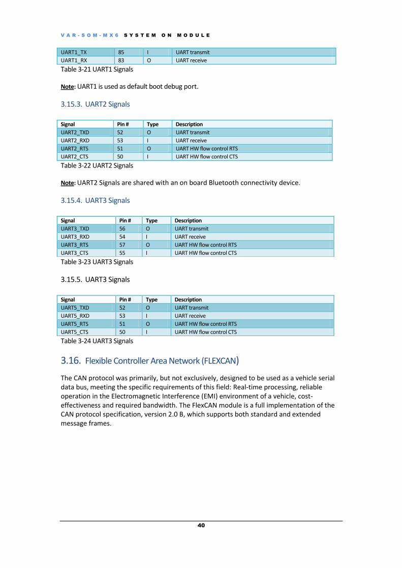
V A R - S O M - M X 6 S Y S T E M O N M O D U L E
40
Table 3-21 UART1 Signals
Note: UART1 is used as default boot debug port.
3.15.3. UART2 Signals
Table 3-22 UART2 Signals
Note: UART2 Signals are shared with an on board Bluetooth connectivity device.
3.15.4. UART3 Signals
Table 3-23 UART3 Signals
3.15.5. UART3 Signals
Table 3-24 UART3 Signals
3.16. Flexible Controller Area Network (FLEXCAN)
The CAN protocol was primarily, but not exclusively, designed to be used as a vehicle serial data bus, meeting the specific requirements of this field: Real-time processing, reliable operation in the Electromagnetic Interference (EMI) environment of a vehicle, cost-effectiveness and required bandwidth. The FlexCAN module is a full implementation of the CAN protocol specification, version 2.0 B, which supports both standard and extended message frames.
UART1_TX 85 I UART transmit
UART1_RX 83 O UART receive
Signal Pin # Type Description
UART2_TXD 52 O UART transmit
UART2_RXD 53 I UART receive
UART2_RTS 51 O UART HW flow control RTS
UART2_CTS 50 I UART HW flow control CTS
Signal Pin # Type Description
UART3_TXD 56 O UART transmit
UART3_RXD 54 I UART receive
UART3_RTS 57 O UART HW flow control RTS
UART3_CTS 55 I UART HW flow control CTS
Signal Pin # Type Description
UART5_TXD 52 O UART transmit
UART5_RXD 53 I UART receive
UART5_RTS 51 O UART HW flow control RTS
UART5_CTS 50 I UART HW flow control CTS
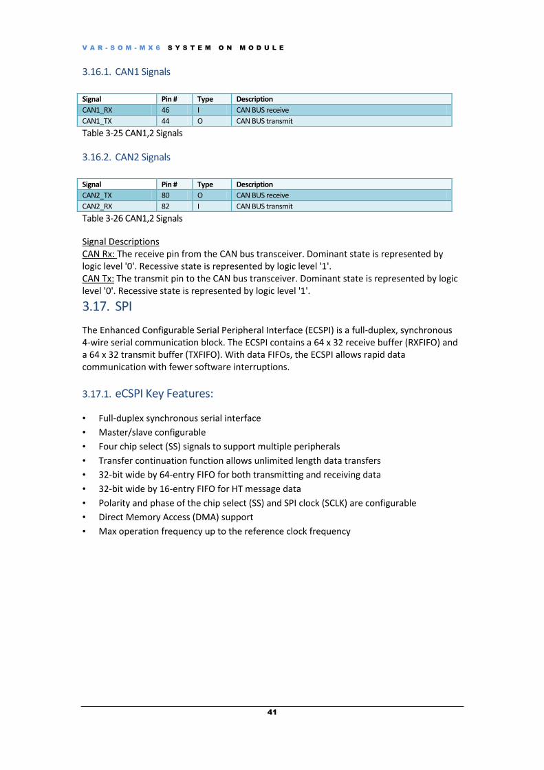
V A R - S O M - M X 6 S Y S T E M O N M O D U L E
41
3.16.1. CAN1 Signals
Table 3-25 CAN1,2 Signals
3.16.2. CAN2 Signals
Table 3-26 CAN1,2 Signals
Signal Descriptions CAN Rx: The receive pin from the CAN bus transceiver. Dominant state is represented by logic level '0'. Recessive state is represented by logic level '1'. CAN Tx: The transmit pin to the CAN bus transceiver. Dominant state is represented by logic level '0'. Recessive state is represented by logic level '1'.
3.17. SPI
The Enhanced Configurable Serial Peripheral Interface (ECSPI) is a full-duplex, synchronous 4-wire serial communication block. The ECSPI contains a 64 x 32 receive buffer (RXFIFO) and a 64 x 32 transmit buffer (TXFIFO). With data FIFOs, the ECSPI allows rapid data communication with fewer software interruptions.
3.17.1. eCSPI Key Features:
• Full-duplex synchronous serial interface
• Master/slave configurable
• Four chip select (SS) signals to support multiple peripherals
• Transfer continuation function allows unlimited length data transfers
• 32-bit wide by 64-entry FIFO for both transmitting and receiving data
• 32-bit wide by 16-entry FIFO for HT message data
• Polarity and phase of the chip select (SS) and SPI clock (SCLK) are configurable
• Direct Memory Access (DMA) support
• Max operation frequency up to the reference clock frequency
Signal Pin # Type Description
CAN1_RX 46 I CAN BUS receive
CAN1_TX 44 O CAN BUS transmit
Signal Pin # Type Description
CAN2_TX 80 O CAN BUS receive
CAN2_RX 82 I CAN BUS transmit
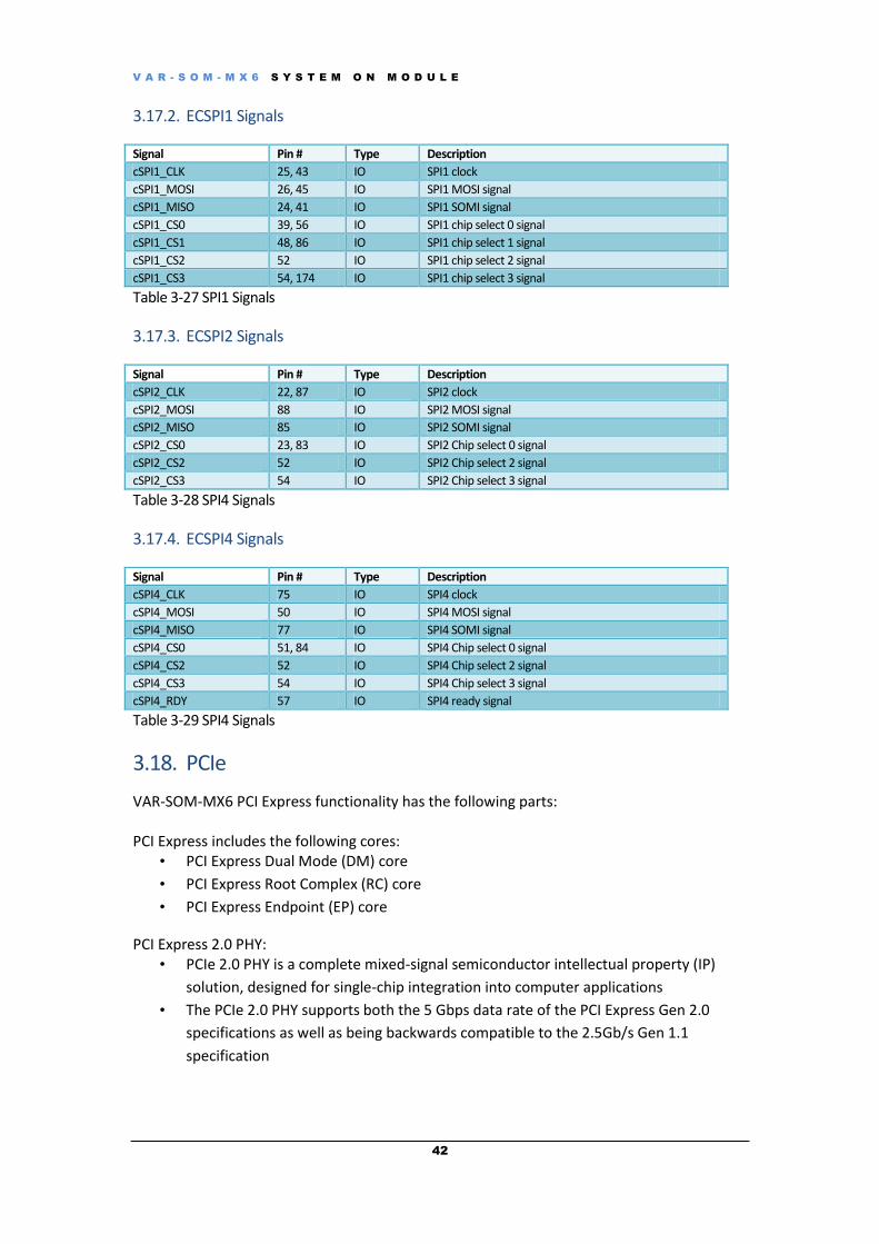
V A R - S O M - M X 6 S Y S T E M O N M O D U L E
42
3.17.2. ECSPI1 Signals
Signal Pin # Type Description
cSPI1_CLK 25, 43 IO SPI1 clock
cSPI1_MOSI 26, 45 IO SPI1 MOSI signal
cSPI1_MISO 24, 41 IO SPI1 SOMI signal
cSPI1_CS0 39, 56 IO SPI1 chip select 0 signal
cSPI1_CS1 48, 86 IO SPI1 chip select 1 signal
cSPI1_CS2 52 IO SPI1 chip select 2 signal
cSPI1_CS3 54, 174 IO SPI1 chip select 3 signal
Table 3-27 SPI1 Signals
3.17.3. ECSPI2 Signals
Signal Pin # Type Description
cSPI2_CLK 22, 87 IO SPI2 clock
cSPI2_MOSI 88 IO SPI2 MOSI signal
cSPI2_MISO 85 IO SPI2 SOMI signal
cSPI2_CS0 23, 83 IO SPI2 Chip select 0 signal
cSPI2_CS2 52 IO SPI2 Chip select 2 signal
cSPI2_CS3 54 IO SPI2 Chip select 3 signal
Table 3-28 SPI4 Signals
3.17.4. ECSPI4 Signals
Signal Pin # Type Description
cSPI4_CLK 75 IO SPI4 clock
cSPI4_MOSI 50 IO SPI4 MOSI signal
cSPI4_MISO 77 IO SPI4 SOMI signal
cSPI4_CS0 51, 84 IO SPI4 Chip select 0 signal
cSPI4_CS2 52 IO SPI4 Chip select 2 signal
cSPI4_CS3 54 IO SPI4 Chip select 3 signal
cSPI4_RDY 57 IO SPI4 ready signal
Table 3-29 SPI4 Signals
3.18. PCIe
VAR-SOM-MX6 PCI Express functionality has the following parts: PCI Express includes the following cores:
• PCI Express Dual Mode (DM) core
• PCI Express Root Complex (RC) core
• PCI Express Endpoint (EP) core
PCI Express 2.0 PHY: • PCIe 2.0 PHY is a complete mixed-signal semiconductor intellectual property (IP)
solution, designed for single-chip integration into computer applications
• The PCIe 2.0 PHY supports both the 5 Gbps data rate of the PCI Express Gen 2.0
specifications as well as being backwards compatible to the 2.5Gb/s Gen 1.1
specification
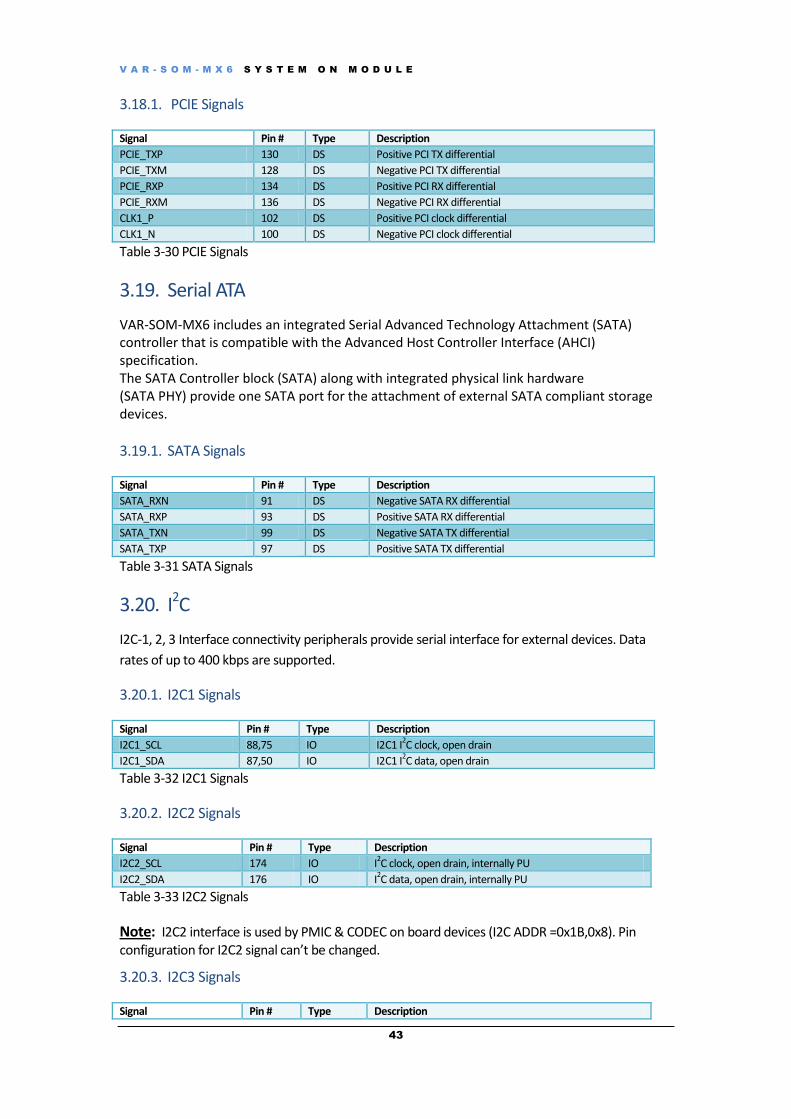
V A R - S O M - M X 6 S Y S T E M O N M O D U L E
43
3.18.1. PCIE Signals
Signal Pin # Type Description
PCIE_TXP 130 DS Positive PCI TX differential
PCIE_TXM 128 DS Negative PCI TX differential
PCIE_RXP 134 DS Positive PCI RX differential
PCIE_RXM 136 DS Negative PCI RX differential
CLK1_P 102 DS Positive PCI clock differential
CLK1_N 100 DS Negative PCI clock differential
Table 3-30 PCIE Signals
3.19. Serial ATA
VAR-SOM-MX6 includes an integrated Serial Advanced Technology Attachment (SATA) controller that is compatible with the Advanced Host Controller Interface (AHCI) specification. The SATA Controller block (SATA) along with integrated physical link hardware (SATA PHY) provide one SATA port for the attachment of external SATA compliant storage devices.
3.19.1. SATA Signals
Signal Pin # Type Description
SATA_RXN 91 DS Negative SATA RX differential
SATA_RXP 93 DS Positive SATA RX differential
SATA_TXN 99 DS Negative SATA TX differential
SATA_TXP 97 DS Positive SATA TX differential
Table 3-31 SATA Signals
3.20. I2C
I2C-1, 2, 3 Interface connectivity peripherals provide serial interface for external devices. Data
rates of up to 400 kbps are supported.
3.20.1. I2C1 Signals
Signal Pin # Type Description
I2C1_SCL 88,75 IO I2C1 I2C clock, open drain
I2C1_SDA 87,50 IO I2C1 I2C data, open drain
Table 3-32 I2C1 Signals
3.20.2. I2C2 Signals
Signal Pin # Type Description
I2C2_SCL 174 IO I2C clock, open drain, internally PU
I2C2_SDA 176 IO I2C data, open drain, internally PU
Table 3-33 I2C2 Signals
Note: I2C2 interface is used by PMIC & CODEC on board devices (I2C ADDR =0x1B,0x8). Pin configuration for I2C2 signal can’t be changed.
3.20.3. I2C3 Signals
Signal Pin # Type Description

V A R - S O M - M X 6 S Y S T E M O N M O D U L E
44
I2C3_SCL 92 IO I2C3 I2C clock, open drain
I2C3_SDA 90 IO I2C3 I2C data, open drain
Table 3-34 I2C3 Signals
3.21. Local Bus
The EIM handles the interface to devices external to the chip, including generation of chip selects, clock and control for external peripherals and memory. It provides asynchronous access to devices with a SRAM-like interface and synchronous access to devices with Nor-Flash-like or PSRAM-like interfaces. The local bus signals are split between two connectors: SODIMM 200 connector and 40-pin FFC connector.
3.21.1. Local Bus Signals SODIMM Connector
Signal Pin # Type Description
WEIM_D[19] 86 IO Local Bus D[19] signal
WEIM_D[20] 84 IO Local Bus D[20] signal
WEIM_D[21] 75 IO Local Bus D[21] signal
WEIM_D[22] 77 IO Local Bus D[22] signal
WEIM_D[23] 55 IO Local Bus D[23] signal
WEIM_D[24] 52 IO Local Bus D[24] signal
WEIM_D[25] 54 IO Local Bus D[25] signal
WEIM_D[27] 53 IO Local Bus D[27] signal
WEIM_D[28] 50 IO Local Bus D[28] signal
WEIM_D[29] 51 IO Local Bus D[29] signal
WEIM_D[30] 79 IO Local Bus D[30] signal
WEIM_DA_A[13] 40 IO Local Bus DA[13] signal
WEIM_EB[2] 56 IO Local Bus EB[2] signal
WEIM_EB[3] 57 IO Local Bus EB[3] signal
WEIM_D[8] 124 IO Local Bus D[8] signal
WEIM_D[9] 175 IO Local Bus D[9] signal
WEIM_D[10] 171 IO Local Bus D[10] signal
WEIM_D[11] 115 IO Local Bus D[11] signal
WEIM_D[12] 173 IO Local Bus D[12] signal
WEIM_D[13] 117 IO Local Bus D[13] signal
WEIM_D[14] 113 IO Local Bus D[14] signal
WEIM_D[15] 96 IO Local Bus D[15] signal
WEIM_D[6] 87 IO Local Bus D[6] signal
WEIM_D[7] 88 IO Local Bus D[7] signal
WEIM_D[0] 122 IO Local Bus D[0] signal
WEIM_D[1] 120 IO Local Bus D[1] signal
WEIM_CS[2] 63 IO Local Bus CS[2] signal
WEIM_CS[3] 61 IO Local Bus CS[3] signal
WEIM_CS[2] 23 IO Local Bus CS[2] signal
WEIM_CS[3] 22 IO Local Bus CS[3] signal
Table 3-35 Local Bus Signals SODIMM 200 Connector
3.21.2. Local Bus Signals 40 Pin FFC connector
Signal Pin # Type Description
WEIM_A[16] 2 IO Local Bus A[16] signal
WEIM_A[17] 6 IO Local Bus A[17] signal
WEIM_WAIT 9 IO Local Bus Wait signal
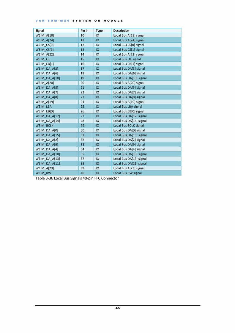
V A R - S O M - M X 6 S Y S T E M O N M O D U L E
45
Signal Pin # Type Description
WEIM_A[18] 10 IO Local Bus A[18] signal
WEIM_A[24] 11 IO Local Bus A[24] signal
WEIM_CS[0] 12 IO Local Bus CS[0] signal
WEIM_CS[1] 13 IO Local Bus CS[1] signal
WEIM_A[22] 14 IO Local Bus A[22] signal
WEIM_OE 15 IO Local Bus OE signal
WEIM_EB[1] 16 IO Local Bus EB[1] signal
WEIM_DA_A[3] 17 IO Local Bus DA[3] signal
WEIM_DA_A[6] 18 IO Local Bus DA[6] signal
WEIM_DA_A[10] 19 IO Local Bus DA[10] signal
WEIM_A[20] 20 IO Local Bus A[20] signal
WEIM_DA_A[5] 21 IO Local Bus DA[5] signal
WEIM_DA_A[7] 22 IO Local Bus DA[7] signal
WEIM_DA_A[8] 23 IO Local Bus DA[8] signal
WEIM_A[19] 24 IO Local Bus A[19] signal
WEIM_LBA 25 IO Local Bus LBA signal
WEIM_EB[0] 26 IO Local Bus EB[0] signal
WEIM_DA_A[12] 27 IO Local Bus DA[12] signal
WEIM_DA_A[14] 28 IO Local Bus DA[14] signal
WEIM_BCLK 29 IO Local Bus BCLK signal
WEIM_DA_A[0] 30 IO Local Bus DA[0] signal
WEIM_DA_A[15] 31 IO Local Bus DA[15] signal
WEIM_DA_A[2] 32 IO Local Bus DA[2] signal
WEIM_DA_A[9] 33 IO Local Bus DA[9] signal
WEIM_DA_A[4] 34 IO Local Bus DA[4] signal
WEIM_DA_A[10] 35 IO Local Bus DA[10] signal
WEIM_DA_A[13] 37 IO Local Bus DA[13] signal
WEIM_DA_A[11] 38 IO Local Bus DA[11] signal
WEIM_A[23] 39 IO Local Bus A[23] signal
WEIM_RW 40 IO Local Bus RW signal
Table 3-36 Local Bus Signals 40-pin FFC Connector

V A R - S O M - M X 6 S Y S T E M O N M O D U L E
46
3.22. JTAG
The System JTAG Controller (SJC) provides debug and test control with maximum security. The test access port (TAP) is designed to support features compatible with the IEEE standard 1149.1 v2001 (JTAG). Support IEEE P1149.6 extensions to the JTAG standard are for AC testing of selected IO signals.
3.22.1. JTAG signals 40-pin FFC Connector
JTAG signal are exposed by the 40-pin FFC connector
Signal Pin # Type Description
JTAG_TDI 1 I JTAG data-in
JTAG_NTRST 3 I JTAG reset
JTAG_TMS 4 I JTAG test mode select
JTAG_TCK 5 O JTAG test clock
JTAG_TDO 7 O JTAG data-out
Table 3-37 JTAG Signals 40-pin FFC Connector
3.23. General Purpose IOs
Most of the SoM's IO pins can be used as GPIOs. See Chapter 3, Table 3.1 and 3.2 for a complete SoM connectors signal list and GPIO multiplexing.
3.24. General System Control
3.24.1. Boot Options
The boot option signal configures the boot sequence of the VAR-SOM-MX6: BOOT_SEL0: Not Connected: Boot device is on NAND Logic ‘0’: Boot device is an off-board SD card, using an SDMMC2 interface. BOOT_SEL1: Future use- leave not connected
3.24.2. Reset
‘0’ logic will reset VAR-SOM-MX6
3.24.3. Reference Clock Out
VAR-SOM-MX6 output clock (CLKO2) is controlled by the i.MX6 CCM module. Please refer to the i.MX6 user manual regarding the configuration option for this clock.
3.24.4. General System Control Signals
Signal Pin # Type Description
CLKO 29 O Clock out
BOOT_SEL0 42 I System boot option select [high – internal device boot]
BOOT_SEL1 40 I Leave NC
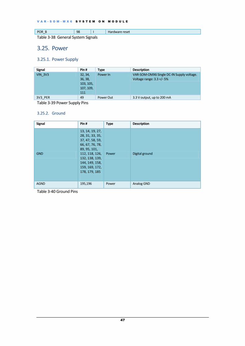
V A R - S O M - M X 6 S Y S T E M O N M O D U L E
47
POR_B 98 I Hardware reset
Table 3-38 General System Signals
3.25. Power
3.25.1. Power Supply
Signal Pin # Type Description
VIN_3V3 32, 34, 36, 38, 103, 105, 107, 109, 111
Power In VAR-SOM-OMX6 Single DC-IN Supply voltage. Voltage range: 3.3 +/- 5%
3V3_PER 49 Power Out 3.3 V output, up to 200 mA
Table 3-39 Power Supply Pins
3.25.2. Ground
Signal Pin # Type Description
GND
13, 14, 19, 27, 28, 31, 33, 35, 37, 47, 58, 59, 66, 67, 76, 78, 89, 95, 101, 112, 118, 126, 132, 138, 139, 144, 149, 158, 159, 169, 172, 178, 179, 185
Power Digital ground
AGND 195,196 Power Analog GND
Table 3-40 Ground Pins

V A R - S O M - M X 6 S Y S T E M O N M O D U L E
48
4. Absolute Maximum Characteristics Power Supply Min Max Unit
Main Power Supply, DC-IN -0.3 3.5 V
Table 4-1 Absolute Maximum Characteristics
5. Operational Characteristics 5.1. Power supplies
Min Typical Max Unit
Main Power Supply, DC-IN -5% 3.3 +5% V
Table 5-1 Power Supplies Operational Characteristics
5.2. Power Consumption
The VAR-SOM-MX6 power consumption is 1.2W typical, when the device is on and the OS is in idle mode.
6. DC Electrical Characteristics
Parameter Min Typical Max Unit
Digital 3.3V
VIH
0.7x VIN_3V3 VIN_3V3 V
VIL 0 0.3x VIN_3V3 V
VOH
VIN_3V3- 0.15 V
VOL
0.15 V
Table 6-1 DC Electrical Characteristics
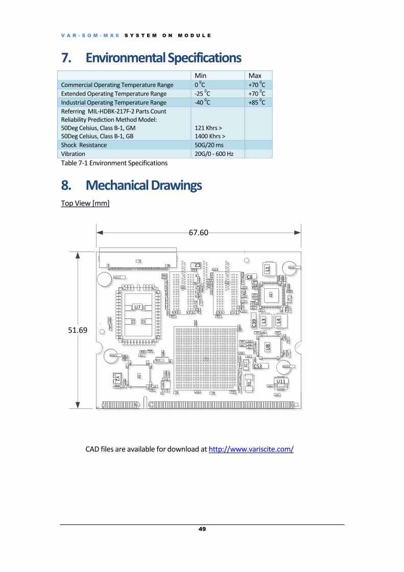
V A R - S O M - M X 6 S Y S T E M O N M O D U L E
49
7. Environmental Specifications Min Max Commercial Operating Temperature Range 0
0C +70
0C
Extended Operating Temperature Range -25 0C +70
0C
Industrial Operating Temperature Range -40 0C +85
0C
Referring MIL-HDBK-217F-2 Parts Count Reliability Prediction Method Model: 50Deg Celsius, Class B-1, GM 50Deg Celsius, Class B-1, GB
121 Khrs > 1400 Khrs >
Shock Resistance 50G/20 ms
Vibration 20G/0 - 600 Hz
Table 7-1 Environment Specifications
8. Mechanical Drawings Top View [mm]
FD*
FD*
L2
J4
1 39 41 199
HOLE1
HOLE2
HOLE4
HOLE3
Y3Y1
Y2
1U
10
81R121
U11
J1
1 40
U8
1 12
13
24
25
36
37
48
U9
14
83
73
6
25
24
13
12
U7
1
16
17 27
28
43
4452
R
N
L
J
G
E
C
8 27 3A
9 1
U3
R
NL
J
G
E
C
8 27 3A
9 1
U2
10
M
25 1
AE
A
U1
L1
L4L3
R122
R6
6
R5
6
R55
R70
R40
R2
1
R1
9
R5R
4
R1
R6
R12
R10
R17R13
R26
R30
R31
R29
R4
1
R35
FB1
R39R33
R34
R71
R6
9
R6
2
R1
5
R3
R1
4
R8
R9
C4
9
C3
8
C8
C2
C53
C3
9
C4
5
C41
C37
C6
C1
2
C14
C1
3
C3
3
C15
C1
6
C3
C23
C2
0
C3
5
C2
2
C2
7
C2
1
C2
6
C1
C2
5
C5
C3
1
C1
7
C29
C3
2
C28
C36
C7
C4
C34
C5
1
C57
C61
C30
C24
C5
2
C5
6
C6
2
C59 C60
C43
C4
7
C4
4
C4
8
C42
C4
0
C5
5
C5
4
C5
8
C4
6
C63
C9
C1
0
C19
C18
C1
1
56
43
42 29
28
15
14
1
U6
67.60
51.69
CAD files are available for download at http://www.variscite.com/
V A R - S O M - M X 6 S Y S T E M O N M O D U L E
50
9. Legal Notice Variscite Ltd. (“Variscite”) products and services are sold subject to Variscite terms and conditions of sale, delivery and payment supplied at the time of order acknowledgement.
Variscite warrants performance of its products to the specifications in effect at the date of shipment. Variscite reserves the right to make changes to its products and specifications or to discontinue any product or service without notice. Customers should therefore obtain the latest version of relevant product information from Variscite to verify that their reference is current.
Testing and other quality control techniques are utilized to the extent that Variscite deems necessary to support its warranty.
Specific testing of all parameters of each device is not necessarily performed unless required by law or regulation.
In order to minimize risks associated with customer applications, the customer must use adequate design and operating safeguards to minimize inherent or procedural hazards. Variscite is not liable for applications assistance or customer product design. The customer is solely responsible for its selection and use of Variscite products. Variscite is not liable for such selection or use or for use of any circuitry other than circuitry entirely embodied in a Variscite product.
Variscite products are not intended for use in life support systems, appliances, nuclear systems or systems where malfunction can reasonably be expected to result in personal injury, death or severe property or environmental damage. Any use of products by the customer for such purposes is at the customer’s own risk.
Variscite does not grant any license (express or implied) under any patent right, copyright, mask work right or other intellectual property right of Variscite covering or relating to any combination, machine, or process in which its products or services might be or are used. Any provision or publication of any third party’s products or services does not constitute Variscite’s approval, license, warranty or endorsement thereof. Any third party trademarks contained in this document belong to the respective third party owner.
Reproduction of information from Variscite datasheets is permissible only if reproduction is without alteration and is accompanied by all associated copyright, proprietary and other notices (including this notice) and conditions. Variscite is not liable for any un-authorized alteration of such information or for any reliance placed thereon.
Any representations made, warranties given, and/or liabilities accepted by any person which differ from those contained in this datasheet or in Variscite’s standard terms and conditions of sale, delivery and payment are made, given and/or accepted at that person’s own risk. Variscite is not liable for any such representations, warranties or liabilities or for any reliance placed thereon by any person.
V A R - S O M - M X 6 S Y S T E M O N M O D U L E
51
10. Warranty Terms Variscite guarantees hardware products against defects in workmanship and material
for a period of one (1) year from the date of shipment. Your sole remedy and Variscite’s
sole liability shall be for Variscite, at its sole discretion, to either repair or replace the
defective hardware product at no charge or to refund the purchase price. Shipment
costs in both directions are the responsibility of the customer. This warranty is void if
the hardware product has been altered or damaged by accident, misuse or abuse.
Disclaimer of Warranty
THIS WARRANTY IS MADE IN LIEU OF ANY OTHER WARRANTY, WHETHER EXPRESSED,
OR IMPLIED, OF MERCHANTABILITY, FITNESS FOR A SPECIFIC PURPOSE, NON-
INFRINGEMENT OR THEIR EQUIVALENTS UNDER THE LAWS OF ANY JURISDICTION,
EXCEPT THE WARRANTY EXPRESSLY STATED HEREIN. THE REMEDIES SET FORTH HEREIN
SHALL BE THE SOLE AND EXCLUSIVE REMEDIES OF ANY PURCHASER WITH RESPECT TO
ANY DEFECTIVE PRODUCT.
Limitation on Liability
UNDER NO CIRCUMSTANCES SHALL VARISCITE BE LIABLE FOR ANY LOSS, DAMAGE OR
EXPENSE SUFFERED OR INCURRED WITH RESPECT TO ANY DEFECTIVE PRODUCT. IN NO
EVENT SHALL VARISCITE BE LIABLE FOR ANY INCIDENTAL OR CONSEQUENTIAL
DAMAGES THAT YOU MAY SUFFER DIRECTLY OR INDIRECTLY FROM USE OF ANY
PRODUCT. BY ORDERING THE SOM, THE CUSTOMER APPROVES THAT THE VARISCITE
SOM, HARDWARE AND SOFTWARE, WAS THOROUGHLY TESTED AND HAS MET THE
CUSTOMER'S REQUIREMETS AND SPECIFICATIONS.

V A R - S O M - M X 6 S Y S T E M O N M O D U L E
52
11. Contact Information
Headquarters: Variscite Ltd. 9, Hamelacha Street Lod P.O.B 1121 Airport City, 70100 ISRAEL Tel: +972 (9) 9562910 Fax: +972 (9) 9589477
Sales: [email protected]
Technical Support: [email protected]
Corporate Website: www.variscite.com