
V2I7_IJERTV2IS70741
4
Simulation Of Bridgeless Buck PFC Converter Rajitha A R M-Tech,(Power Electronics),Electrical Engineering Department, Mar Athanasius College Of Engineering,Kothamangalam Abstract Conventional buck power factor correction rectifiers have high conduction losses and switching losses due to the presence of input rectifier bridges. The bridgeless buck converter improves the efficiency by reducing the conduction losses by using lesser number of semiconductor devices. This circuit also works as a voltage doubler circuit. Although the output voltage is doubled the switching losses of the devices connected at the dc/dc output stage is lower than the boost power factor correction rectifier. This paper presents simulation of bridgeless PFC buck converter in MATLAB software. Keywords - Power factor correction (PFC), Bridgeless rectification, buck converter, conduction loss, switching loss 1.Introduction Presently, maintaining high efficiency along the entire line range (90-264V) becomes a challenge for the ac- dc converters that are used for power factor correction. There is also requirement of high power factor and low total harmonic distortion in the current drawn from the utility. Various topologies have been introduced in this respect for attaining high power factor and low harmonic distortion. The boost topology was the widely used topology at the earlier stage.Conventional boost bridge PFC rectifier comprises of full bridge rectifier followed by a boost converter. This bridge arrangement has high conduction losses due to the number of semiconductor devices and hence the efficiency is less. To reduce this loss a bridgeless boost topology[3] was introduced which eliminates the use of bridge rectifier. Even though boost PFC is efficient, the output voltage of boost converter is greater than the input which facilitates the use of higher rating semiconductor devices at the downstream. The drawback of universal line boost PFC front end can be overcome by implementing buck PFC topology[2]. This paper analyses the bridgeless buck converter which further improves the efficiency of the buck converter[1] by minimizing the number of simultaneously conducting devices. This converter also works as a voltage doubler circuit whose output voltage is twice the input voltage.Eventhough the output voltage is doubled the switching losses at the downstream is lower than the boost frontend. The bridgeless PFC buck topology improves efficiency at low line of the universal line range than the bridgeless boost PFC rectifier. 2.Bridgeless PFC circuit The circuit of a bridgeless buck converter is shown in fig 1. Here two buck converters are connected in back to back. During positive half cycle buck converter consisting of switch S1,diode D1,freewheeling diode D3,Inductor L1,Capacitor C1 operates. The voltage across C1 is regulated by pulse width modulation of the switch S1.During negative half cycle switch S2,freewheeling diode D4,diode D3,Inductor L2 and capacitor C2 operates. Here the output voltage across C2 is regulated by pulse width modulation of switch S2.The voltage available at the output resistor is the sum of the voltages across capacitors C1&C2. Fig.1.Bridgeless PFC converter Since the output voltage of the bridgeless buck converter is the sum of voltage across two capacitors Vo=2DVin 2188 International Journal of Engineering Research & Technology (IJERT) Vol. 2 Issue 7, July - 2013 ISSN: 2278-0181 www.ijert.org IJERTV2IS70741
-
Upload
guru87joshi3473 -
Category
Documents
-
view
212 -
download
0
description
BUCK CONVERTER
Transcript of V2I7_IJERTV2IS70741

Simulation Of Bridgeless Buck PFC Converter Rajitha A R
M-Tech,(Power Electronics),Electrical Engineering Department, Mar Athanasius College Of
Engineering,Kothamangalam
Abstract
Conventional buck power factor correction rectifiers
have high conduction losses and switching losses due
to the presence of input rectifier bridges. The
bridgeless buck converter improves the efficiency by
reducing the conduction losses by using lesser
number of semiconductor devices. This circuit also
works as a voltage doubler circuit. Although the
output voltage is doubled the switching losses of the
devices connected at the dc/dc output stage is lower
than the boost power factor correction rectifier. This
paper presents simulation of bridgeless PFC buck
converter in MATLAB software.
Keywords - Power factor correction (PFC),
Bridgeless rectification, buck converter,
conduction loss, switching loss
1.Introduction
Presently, maintaining high efficiency along the entire
line range (90-264V) becomes a challenge for the ac-
dc converters that are used for power factor correction.
There is also requirement of high power factor and low
total harmonic distortion in the current drawn from the
utility. Various topologies have been introduced in this
respect for attaining high power factor and low
harmonic distortion.
The boost topology was the widely used topology at
the earlier stage.Conventional boost bridge PFC
rectifier comprises of full bridge rectifier followed by a
boost converter. This bridge arrangement has high
conduction losses due to the number of semiconductor
devices and hence the efficiency is less. To reduce this
loss a bridgeless boost topology[3] was introduced
which eliminates the use of bridge rectifier.
Even though boost PFC is efficient, the output voltage
of boost converter is greater than the input which
facilitates the use of higher rating semiconductor
devices at the downstream. The drawback of universal
line boost PFC front end can be overcome by
implementing buck PFC topology[2]. This paper
analyses the bridgeless buck converter which further
improves the efficiency of the buck converter[1] by
minimizing the number of simultaneously conducting
devices. This converter also works as a voltage doubler
circuit whose output voltage is twice the input
voltage.Eventhough the output voltage is doubled the
switching losses at the downstream is lower than the
boost frontend.
The bridgeless PFC buck topology improves
efficiency at low line of the universal line range than
the bridgeless boost PFC rectifier.
2.Bridgeless PFC circuit
The circuit of a bridgeless buck converter is shown in
fig 1. Here two buck converters are connected in back
to back. During positive half cycle buck converter
consisting of switch S1,diode D1,freewheeling diode
D3,Inductor L1,Capacitor C1 operates. The voltage
across C1 is regulated by pulse width modulation of the
switch S1.During negative half cycle switch
S2,freewheeling diode D4,diode D3,Inductor L2 and
capacitor C2 operates. Here the output voltage across
C2 is regulated by pulse width modulation of switch
S2.The voltage available at the output resistor is the
sum of the voltages across capacitors C1&C2.
Fig.1.Bridgeless PFC converter
Since the output voltage of the bridgeless buck
converter is the sum of voltage across two capacitors
Vo=2DVin
2188
International Journal of Engineering Research & Technology (IJERT)
Vol. 2 Issue 7, July - 2013
IJERT
IJERT
ISSN: 2278-0181
www.ijert.orgIJERTV2IS70741
2.1.Positive half cycle:
During positive half cycle the buck converter
comprising of diode D1,switch S1,inductor
L1,capacitor C1 and freewheeling diode D3 is
operating. When switch S1 is on, the inductor L1
stores energy and the current path is through diode
D1,switch,inductor L1,capacitor C1.When the
switch is off the current freewheels through the
diode D3.The voltage across the capacitor is
regulated by the pulse width modulation of switch
S1.The buck converter which is operating during
positive half cycle is shown in bold lines.
Fig.2.Operation during positive half cycle
2. Negative half cycle:
During the negative half cycle the buck converter
consisting of switch S2,diode D2,inductor
L2,capacitor C2 and the freewheeling diode D3
operates. When the switch is on the inductor L2
stores energy and when the switch is off, the energy
is discharged through the freewheeling diode
D4.The output voltage of each buck converter is
available across the capacitors. Since the direction
of current is in the same direction in both the
capacitors, the output voltage obtained across the
load resistor is twice the voltage obtained at any of
the buck converter. The buck converter operating
during the negative half of the line voltage is
shown in bold lines in the figure given below
Fig.3.Operation during negative half cycle
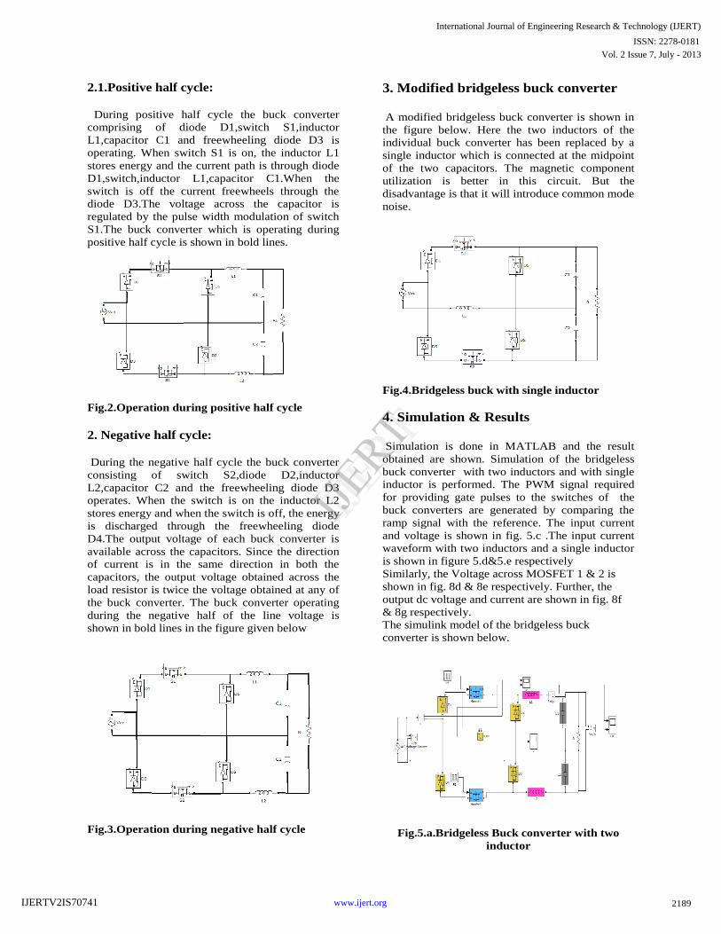
3. Modified bridgeless buck converter
A modified bridgeless buck converter is shown in
the figure below. Here the two inductors of the
individual buck converter has been replaced by a
single inductor which is connected at the midpoint
of the two capacitors. The magnetic component
utilization is better in this circuit. But the
disadvantage is that it will introduce common mode
noise.
Fig.4.Bridgeless buck with single inductor
4. Simulation & Results
Simulation is done in MATLAB and the result
obtained are shown. Simulation of the bridgeless
buck converter with two inductors and with single
inductor is performed. The PWM signal required
for providing gate pulses to the switches of the
buck converters are generated by comparing the
ramp signal with the reference. The input current
and voltage is shown in fig. 5.c .The input current
waveform with two inductors and a single inductor
is shown in figure 5.d&5.e respectively
Similarly, the Voltage across MOSFET 1 & 2 is
shown in fig. 8d & 8e respectively. Further, the
output dc voltage and current are shown in fig. 8f
& 8g respectively.
The simulink model of the bridgeless buck
converter is shown below.
Fig.5.a.Bridgeless Buck converter with two
inductor
2189
International Journal of Engineering Research & Technology (IJERT)
Vol. 2 Issue 7, July - 2013
IJERT
IJERT
ISSN: 2278-0181
www.ijert.orgIJERTV2IS70741

The simulink model of bridgeless buck converter
with single inductor is as shown
Fig.5.b.Bridgeless buck converter with single
inductor
Fig.5.c.Input voltage and current waveform
Fig.5.d.Input current waveform with two
inductors
Fig.5.e.Input current waveform with single
inductor
Fig.5.f.PWM across switches
Fig.5.g.Voltage across switches S1&S2
2190
International Journal of Engineering Research & Technology (IJERT)
Vol. 2 Issue 7, July - 2013
IJERT
IJERT
ISSN: 2278-0181
www.ijert.orgIJERTV2IS70741

Fig.5.h.Output voltage waveform
5. Conclusion
In this paper a bridgeless buck PFC converter with
two inductors and with single inductor has been
analysed, modelled and simulated in matlab.This
bridgeless PFC is having two buck converters
connected back to back. since number of
conducting devices are less as compared to the
bridge circuit the conduction losses and switching
losses are less. The input current and voltages are
almost in phase which represents a high power
factor. The single inductor topology is having
higher common mode noise as compared to the two
inductor topology even though the magnetic
utilization is better.
REFERENCES [1]1. Yungtaek Jang,Milan M Jovanovic “Bridgeless
High Power Factor Buck Converter,” IEEE Trans. Power
Electron., vol. 26, no. 2, p602–611, Feb. 2011.
[2] L. Huber, L. Gang, and M. M. Jovanovi´c, “Design-
Oriented analysis and performance evaluation of buck
PFC front-end,” IEEE Trans. PowerElectron., vol. 25,
no. 1, pp. 85–94, Jan. 2010.
[3]J. C. Salmon, “Circuit topologies for single-phase
voltage-doubler boost rectifiers,” IEEE Trans. Power
Electron., vol. 8, no. 4, pp. 521–529, Oct.
[4] H. Endo, T. Yamashita, and T. Sugiura, “A high-
power-factor buck converter,” in Proc. IEEE Power
Electron. Spec. Conf. (PESC) Rec., Jun. 1992, pp. 1071–
1076
[5].G. Spiazzi, “Analysis of buck converters used as
power factor preregulators,” in Proc. IEEE Power
Electron. Spec. Conf. (PESC) Rec., Jun. 1997,
[6] M.Gopinath, “Bridgeless PFC converter for power
factor correction”, International Journal of Advanced
Engineering Sciences and Technologies, Vol No. 9, Issue
No.1, ISSN: 2230-7818, pp. 049-054.
2191
International Journal of Engineering Research & Technology (IJERT)
Vol. 2 Issue 7, July - 2013
IJERT
IJERT
ISSN: 2278-0181
www.ijert.orgIJERTV2IS70741


