Using JEI format
7
Structural Analysis of Submicrometer LiCoO 2 Films P. J. Bouwman, a,z B. A. Boukamp, a, * H. J. M. Bouwmeester, a H. J. Wondergem, b and P. H. L. Notten c, * a Laboratory of Inorganic Materials Science, Faculty of Chemical Technology and MESA Research Institute, University of Twente, 7500 AE Enschede, The Netherlands b Center for Fabrication Technology, c Philips Research Laboratory, 5656 AA Eindhoven, The Netherlands Submicrometer LiCoO 2 films were prepared with pulsed laser deposition ~PLD! and rf sputtering using stoichiometric targets. The influences of both substrate material and annealing procedure on the polycrystalline microstructure of the LiCoO 2 films were investigated. XRD analysis revealed strong preferential orientation: annealed films deposited with PLD had their ~00l! planes parallel to the surface, while rf sputtered films had their ~110! planes in this orientation. The rf-film also developed the ~003! reflection typical of PLD-films, but only after prolonged annealing at 600°C. The degree of preferential orientation is influenced significantly by the annealing procedure and only little by the substrate material and the thickness of the deposited film. Pulsed laser deposition on an rf-sputtered seed layer revealed the PLD-film reflections. Extinction of the otherwise dominating ~003! reflection indicated a random cationic distribution in LiCoO 2 with an NaCl-type structure. © 2001 The Electrochemical Society. @DOI: 10.1149/1.1353570# All rights reserved. Manuscript submitted September 10, 2000; revised manuscript received December 7, 2000. The lithium intercalation ability of LiCoO 2 was discovered 20 years ago by Goodenough and has been exploited by Sony with the introduction of their rechargeable C/LiCoO 2 battery in 1991. Pres- ently, this technology finds large-scale commercial application as a power source for numerous handheld devices. Extensive research has been conducted to explore alternative materials, which are more cost effective and less toxic. 1 Until now, lithium cobalt oxide based electrodes exhibit superior properties in terms of cycle stability and energy density, a favorable combination for a reliable power source. 2,3 There is a growing interest in the production of secondary lithium batteries of smaller dimensions; microbatteries are very suit- able to provide backup power for on-chip static memory modules. Integrated memory is encountered frequently due to a growing ten- dency in the microelectronics industry toward complete integration of all functions onto a single chip designed for one specific purpose. For example, a motor controller chip will contain everything from controller to the power regulation in one module called a multichip module ~MCM!. The functions can subsequently be implemented on a separate silicon substrate, interconnected, and stacked in a single housing. 4 The addition of a single microbattery allows the digital memory states to remain unaffected during power failure or long time storage. The common composite powder electrodes are unsuitable for mi- crobattery application due to their porosity and the necessity for additives. The indistinct characteristics of powder-based electrodes also make modeling of the electrochemical intercalation behavior difficult. The present paper describes preparation and properties of dense, submicron films of polycrystalline LiCoO 2 on a silicon wafer with pulsed laser deposition ~PLD! and rf sputtering. The well- defined composition, microstructure, and dimensions of the depos- ited layers make these samples suitable for fundamental electro- chemical studies of the lithium intercalation process. Eventually, these films could find an application as a positive electrode in mi- crobattery stacks. In this paper we provide a structural characteriza- tion of the LiCoO 2 films in all stages of preparation from deposition to annealing treatment. The favorable electrochemical properties of the LiCoO 2 films will be published in a forthcoming paper. Experimental Thin film deposition.—Submicrometer LiCoO 2 films were pro- duced with pulsed laser deposition and rf sputtering using identical LiCoO 2 targets prepared by solid-state reaction. The composition was analyzed and proved to be stoichiometric. In PLD a 193 nm ArF excimer laser was operated at 5 Hz rep- etition rate and focused to a beam intensity of 2 J cm 22 . Ablation was performed with a counter rotating target and substrate, located at 6 cm distance from each other. A background pressure of 0.2 mbar p O 2 was maintained. At these conditions the deposition rate was approximately 20 Å min 21 . The substrate holder could be heated to temperatures as high as 700°C. The substrate temperature during deposition was 300°C. In situ annealing was performed by increasing the temperature to 600°C for 30 min with 5°C min 21 . After cooling to room temperature the samples were exposed to the ambient. RF sputtering conditions were substrate temperature, 300°C; argon-oxygen background pressure of 7 mTorr in 3:1 ratio; rf power, 50 W; and target-to-substrate distance, 6 cm. At these con- ditions the growth rate of the oxide layer was of the order of 5 Å/min 21 . Annealing treatment of all rf-sputtered samples was per- formed ex situ. Samples were heated with 2°C min 21 to 400 or 600°C in stagnant air or in a constant gas flow containing 90% O 2 /10% N 2 with a flow of 60 mL min 21 STP. Typical annealing times were 30 or 180 min and are referred to as short and prolonged annealing treatment, respectively. Rapid thermal annealing ~RTA! experiments were conducted in nitrogen ambient in a commercial STEAG SHS1000 machine as described by van de Leest et al. 5 In this case the annealing time was 1 min and the applied heating and cooling rate was 10°C s 21 . Silicon wafers ~6 in. diam, ~100! orientation! served as substrate material for both deposition techniques. The polished surface was ion-implanted with antimony to obtain n-type electronic conductiv- ity. The wafer was then laser cut into 15 mm diam disk. The back side and rim of these disks were covered with 0.15 mm aluminum using rf sputtering. This metallic film served as electrical back side contact for electrochemical measurements, connecting the probe with the conducting silicon. In several cases an additional aluminum film ~0.15 mm! was sputtered as the current collector together with an adhesion layer of 50 Å titanium prior to deposition of the LiCoO 2 film. Note that this substrate stack is subjected to the same tempera- ture program as the LiCoO 2 film. The use of aluminum ~as the current collector! limits the upper annealing temperature to its melt- ing point of 660.4°C. Even at temperatures below this value one must be aware of possible interdiffusion of soluble species in the * Electrochemical Society Active Member. z E-mail: [email protected] Journal of The Electrochemical Society, 148 ~4! A311-A317 ~2001! 0013-4651/2001/148~4!/A311/7/$7.00 © The Electrochemical Society, Inc. A311
Transcript of Using JEI format

Journal of The Electrochemical Society, 148 ~4! A311-A317 ~2001!0013-4651/2001/148~4!/A311/7/$7.00 © The Electrochemical Society, Inc.
A311
Structural Analysis of Submicrometer LiCoO2 FilmsP. J. Bouwman,a,z B. A. Boukamp,a,* H. J. M. Bouwmeester,a H. J. Wondergem,b
and P. H. L. Nottenc,*aLaboratory of Inorganic Materials Science, Faculty of Chemical Technology and MESA Research Institute,University of Twente, 7500 AE Enschede, The NetherlandsbCenter for Fabrication Technology,cPhilips Research Laboratory, 5656 AA Eindhoven, The Netherlands
Submicrometer LiCoO2 films were prepared with pulsed laser deposition~PLD! and rf sputtering using stoichiometric targets. Theinfluences of both substrate material and annealing procedure on the polycrystalline microstructure of the LiCoO2 films wereinvestigated. XRD analysis revealed strong preferential orientation: annealed films deposited with PLD had their~00l! planesparallel to the surface, while rf sputtered films had their~110! planes in this orientation. The rf-film also developed the~003!reflection typical of PLD-films, but only after prolonged annealing at 600°C. The degree of preferential orientation is influencedsignificantly by the annealing procedure and only little by the substrate material and the thickness of the deposited film. Pulsedlaser deposition on an rf-sputtered seed layer revealed the PLD-film reflections. Extinction of the otherwise dominating~003!reflection indicated a random cationic distribution in LiCoO2 with an NaCl-type structure.© 2001 The Electrochemical Society.@DOI: 10.1149/1.1353570# All rights reserved.
Manuscript submitted September 10, 2000; revised manuscript received December 7, 2000.
t
sar
mo
ane
aryuitlestentionsemhiponin
alng
mfode
vios
poctrllymirizns
icaltion
ep-
ated0.2
ateeraturey
the
°C;rf
con-f 5er-
0%
ged
cial
and
ewasiv-ck
iderobeumith
Oera-
lt-onethe
The lithium intercalation ability of LiCoO2 was discovered 20years ago by Goodenough and has been exploited by Sony withintroduction of their rechargeable C/LiCoO2 battery in 1991. Pres-ently, this technology finds large-scale commercial application apower source for numerous handheld devices. Extensive resehas been conducted to explore alternative materials, which arecost effective and less toxic.1 Until now, lithium cobalt oxide basedelectrodes exhibit superior properties in terms of cycle stabilityenergy density, a favorable combination for a reliable powsource.2,3
There is a growing interest in the production of secondlithium batteries of smaller dimensions; microbatteries are very sable to provide backup power for on-chip static memory moduIntegrated memory is encountered frequently due to a growingdency in the microelectronics industry toward complete integraof all functions onto a single chip designed for one specific purpoFor example, a motor controller chip will contain everything frocontroller to the power regulation in one module called a multicmodule~MCM!. The functions can subsequently be implementeda separate silicon substrate, interconnected, and stacked in a shousing.4 The addition of a single microbattery allows the digitmemory states to remain unaffected during power failure or lotime storage.
The common composite powder electrodes are unsuitable forcrobattery application due to their porosity and the necessityadditives. The indistinct characteristics of powder-based electroalso make modeling of the electrochemical intercalation behadifficult. The present paper describes preparation and propertiedense, submicron films of polycrystalline LiCoO2 on a silicon waferwith pulsed laser deposition~PLD! and rf sputtering. The well-defined composition, microstructure, and dimensions of the deited layers make these samples suitable for fundamental elechemical studies of the lithium intercalation process. Eventuathese films could find an application as a positive electrode incrobattery stacks. In this paper we provide a structural charactetion of the LiCoO2 films in all stages of preparation from depositioto annealing treatment. The favorable electrochemical propertiethe LiCoO2 films will be published in a forthcoming paper.
* Electrochemical Society Active Member.z E-mail: [email protected]
he
achre
dr
-.-
.
gle
i-rsrof
s-o-,-a-
of
Experimental
Thin film deposition.—Submicrometer LiCoO2 films were pro-duced with pulsed laser deposition and rf sputtering using identLiCoO2 targets prepared by solid-state reaction. The composiwas analyzed and proved to be stoichiometric.
In PLD a 193 nm ArF excimer laser was operated at 5 Hz retition rate and focused to a beam intensity of 2 J cm22. Ablationwas performed with a counter rotating target and substrate, locat 6 cm distance from each other. A background pressure ofmbar pO2
was maintained. At these conditions the deposition rwas approximately 20 Å min21. The substrate holder could bheated to temperatures as high as 700°C. The substrate tempeduring deposition was 300°C.In situ annealing was performed bincreasing the temperature to 600°C for 30 min with 5°C min21.After cooling to room temperature the samples were exposed toambient.
RF sputtering conditions were substrate temperature, 300argon-oxygen background pressure of 7 mTorr in 3:1 ratio;power, 50 W; and target-to-substrate distance, 6 cm. At theseditions the growth rate of the oxide layer was of the order oÅ/min21. Annealing treatment of all rf-sputtered samples was pformed ex situ. Samples were heated with 2°C min21 to 400 or600°C in stagnant air or in a constant gas flow containing 9O2/10% N2 with a flow of 60 mL min21 STP. Typical annealingtimes were 30 or 180 min and are referred to as short and prolonannealing treatment, respectively. Rapid thermal annealing~RTA!experiments were conducted in nitrogen ambient in a commerSTEAG SHS1000 machine as described by van de Leestet al.5 Inthis case the annealing time was 1 min and the applied heatingcooling rate was 10°C s21.
Silicon wafers~6 in. diam,~100! orientation! served as substratmaterial for both deposition techniques. The polished surfaceion-implanted with antimony to obtain n-type electronic conductity. The wafer was then laser cut into 15 mm diam disk. The baside and rim of these disks were covered with 0.15mm aluminumusing rf sputtering. This metallic film served as electrical back scontact for electrochemical measurements, connecting the pwith the conducting silicon. In several cases an additional aluminfilm ~0.15 mm! was sputtered as the current collector together wan adhesion layer of 50 Å titanium prior to deposition of the LiCo2film. Note that this substrate stack is subjected to the same tempture program as the LiCoO2 film. The use of aluminum~as thecurrent collector! limits the upper annealing temperature to its meing point of 660.4°C. Even at temperatures below this valuemust be aware of possible interdiffusion of soluble species in

the
er
ithuaOL
troed
re
becroas
0°lle-
e rlot,seonleT
LDtheateaynb-pleth
ity,
s,
edgfilmtio
ea
c-as-
ng at
e
y
ith
ure
obalt
Journal of The Electrochemical Society, 148 ~4! A311-A317 ~2001!A312
individual stack layers. The time and temperature window ofthin film annealing process is therefore limited.
Structural analysis.—The crystal structure of the submicrometfilm was analyzed with X-ray diffraction~XRD! using Cu Ka atroom temperature with a Philips PW 1800 diffractometer fitted wa spinning sample holder and an automatic divergence slit. Visization of the film surface morphology was performed using a JEJSM 5800 scanning electron microscope~SEM!. A PhilipsCM30ST, operated at 300 kV, accommodated transmission elecmicroscopy~TEM! analysis on cross sections of rf film preparwith focused ion beam~FIB! thinning.
Results and Discussion
Structural characterization.—Generally, the LiCoO2 host inter-calation matrix is regarded to be derived from the NaCl structuThe structure is rhombohedral~space groupR3m! with atoms in thefollowing positions: cobalt atoms in 3a sites~0, 0, 0!, lithium atomsin 3b ~0, 0, 1/2!, and oxygen in 6c sites6 (0, 0, z) with z> 0.25. Cobalt and lithium alternately occupy octahedral sites
tween adjacent close-packed planes of oxygen. The hexagonalsection~110! is shown in Fig. 1. This ordered structure is knownthe high-temperature~HT! phase of LiCoO2, since it develops dur-ing synthesis or annealing treatment at temperatures above 60Once formed it remains stable at room temperature. The so-calow-temperature~LT! modification is produced with low temperature synthesis methods and is slightly disordered; it comprises 6%the cobalt ions in lithium sites. LT-LiCoO2 transforms intoHT-LiCoO2 upon annealing at temperatures around 600°C.6,7
In Fig. 2 the reference XRD spectrum of the HT-LiCoO2 powderis displayed. The bar labels indicate the associated lattice planflections. In the same graph two typical diffraction spectra are pted of annealed LiCoO2 films deposited with rf sputtering and PLDrespectively. The 2u values of all reflections observed match thoin the reference spectrum with an accuracy of 0.04°. The two strdiffraction maxima at 2u 5 33 and 69° can be ascribed to the singcrystalline silicon substrate and have been indicated as such.peak located at 31.3° in the rf film spectrum is probably Co3O4~220!.
Not all diffraction peaks, characteristic of LiCoO2, are detectedand also different reflections are observed for rf films and Pfilms. Due to the scanning geometry of the XRD equipment onlydiffraction of the lattice planes oriented parallel to the substrsurface is observed~the detection angle is kept equal to the X-rangle of incidence!. A random unit cell orientation, as is commofor powders, will result in a typical XRD powder pattern. The asence of specific diffraction intensities revealed that both samexhibited strong preferential orientation. However, in the case ofrf film the ~110! lattice plane reflection showed the highest intenswhile in case of the PLD film the~003! reflection was the majordiffraction peak. Virtually no other LiCoO2 diffraction maxima weredetected. This indicates that the rf films have their~110! planesparallel to the substrate surface~c axis of the unit cell in plane offilm!. This orientation is perpendicular to that of the PLD filmwhich have their~00l! planes parallel to the substrate surface~c axisof the unit cell normal to film surface!.
The alignment of the unit cell toward the substrate is visualizin Fig. 3 for the PLD film and rf film, respectively. The reflectinlattice planes are indicated. Changing deposition conditions andthickness had only an influence on the degree of crystal orientaThis is discussed in the following paragraphs.
Influence of annealing temperature.—In Fig. 4 the XRD spectraof 0.5 mm rf films are shown as-deposited and after annealing trment at 400 and at 600°C for 3 h~prolonged annealing!. Smallcrystallites were already formed during deposition at 300°C~sub-strate temperature! as revealed by the broad, low intensity refletions at 2u angles 36.5 and 65°. The XRD spectrum of thedeposited PLD film~not shown here! had similar broad diffraction
l-
n
.
-ss
C.d
of
e--
g
he
se
n.
t-
peaks, but these were located around the positions of the~00l! re-flection. Annealing the rf film at 400°C for 3 h introduced additionalbroad reflections, ascribed to the~00l! and ~104! planes of the rocksalt structure. Peak sharpening occurred after prolonged anneali600°C, revealing distinct diffraction peaks. The~110! reflection re-tained the highest intensity, followed by the~003!. The presence ofa small amount of Co3O4 is suggested by the occurrence of the~220!peak at 31.3° and a second~400! peak at 44.8°, which appears as thleft shoulder of the~104! peak of LiCoO2.
The existence of the HT-LiCoO2 intercalation phase is generallconfirmed by a distinct separation of the~110! and~018! reflectionsof a randomly oriented powder sample.8 The c/a ratio of the unitcell determines the position of these reflections. LT-LiCoO2 is con-sidered an ordered, cubic NaCl structure of the spinel type woverlapping~110! and~018! peaks@classified as the~440! reflectionin space groupFd3m]. An ideal close-packed lattice exhibits ac/aratio of 2A6 5 4.899. In the case of the layered hexagonal structof HT-LiCoO2 the c/a ratio is reported to be~14.05/2.8155!
Figure 1. Cross section of the LiCoO2 unit cell along the hexagonal~110!plane. This representation visualizes the octahedral coordination of the c~3a sites! and the lithium~3b sites! cations by oxygen~6c sites!. Note thethreefold rotation symmetry of the axes in thec direction.
eng
didlms
and
3D
bers-
ich
hety
y an
f
t
e
s it
C as
ittle
eal
-
f
Journal of The Electrochemical Society, 148 ~4! A311-A317 ~2001! A313
4.9919 which results in separation of the~110! and~018! reflections.The rf films only revealed the~110! reflection. The dominant naturof this reflection makes it difficult to discern whether peak splitti
Figure 2. XRD spectra of typical submicrometer LiCoO2 films deposited onsilicon substrates with rf sputtering and pulsed laser deposition and annat 600°C for 30 min.
Figure 3. Schematic drawing showing the LiCoO2 unit cell orientation whendeposited with rf sputtering~left! and with PLD~right!.
Figure 4. XRD spectra of three 0.5mm rf films at different stages of preparation: as-deposited at 300°C and after annealing for 3 h in air at 400 and600°C, respectively~spectra vertically displaced for clarity!.
had not occurred yet or whether the~018! diffraction was out of thedetection plane due to preferred orientation. Annealing at 900°Cnot result in noticeable peak separation. The annealed PLD fishowed neither the~110! nor the~018! reflection. However, the rffilms annealed at 600°C for 3 h showed both the~003! and ~110!diffraction peaks. This allowed calculation of thec/a ratio and avalue of 4.894 was obtained, which suggests cubic symmetrythe absence of~110! and ~018! peak splitting.
An X-ray texture analysis was performed to visualize theorientation of the~110! planes on a 0.75mm rf film annealed only ashort time at 600°C. The pole plot, shown in Fig. 5, indicates a fitexture with a fixed~110! plane alignment. The major intensity irecorded at tilting anglew 5 0° and corresponds with the diffraction peak initially observed in the standard XRD spectrum~Fig. 2!.An omega scan of this peak revealed a fwhm value of 6.25°, whindicates a sharp orientation distribution. Also atw 5 60° diffrac-tion intensity is recorded at all rotation angles originating from tother two orientations of the~110! plane within the hexagonal unicell. Consequently, the~104! planes show sharp diffraction intensitat w 5 45°. Although the~003! peak diffraction, occurring atw5 90°, is technically undetectable, its presence was indicated b
intensity increase observed atw 5 85°.In this crystal alignment the required~018! diffraction is to be
expected at w 5 60°. The peak is indeed detected at 2u5 65.31°, well separated from the~110! reflection at 2u5 66.33°. The~018! reflection intensity is slightly less than that o
the ~110! planes (fwhm(018),(110) 5 0.80). Using the 2u values thec/a ratio equals~14.085/2.8165! 5.002, which is in good agreemenwith the corresponding value of~14.079/2.8185! 4.996 calculatedfrom the ~110! and ~104! diffraction angles, measured during thpreceding texture analysis~2u 5 45.18°, recorded atw 5 45°!.Both ratios are close to the reported literature value of 4.991. Thuis assumed that the phase transformation to HT-LiCoO2 in thin filmsis possible and has occurred during annealing treatment at 600°has been reported for LiCoO2 powders.
The oxygen background pressure during film deposition had linfluence on the postanneal XRD spectrum. TestedpO2
values
ed
Figure 5. XRD texture analysis of the~110! diffraction of a 0.75mm rf film~annealed at 600°C, 30 min! visualized in a Wulff projection. Light shades ogray represent high intensity.
Journal of The Electrochemical Society, 148 ~4! A311-A317 ~2001!A314
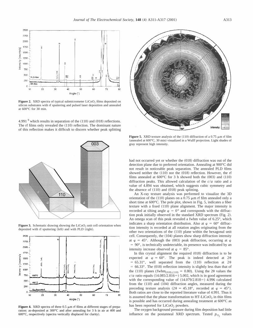
Figure 6. SEM micrographs showing the cross sections of rf films~60° tilt!: 0.5 mm LiCoO2 on 0.15mm Al, as-deposited with rf sputtering~A! and afterannealing at 600°C for 30 min~B!, and 0.75mm LiCoO2 on 0.15mm Al after annealing at 600°C in air for 30 min~C! and 3 h~D!, respectively.
-
ol
uri
gctid
ethe
i-plees
the
sen-
to and
of
n--the
A.linevis-C,col-
.25,
e rf
EMtal-hethe
ranged between 1.1027 and 5.1027 mbar for rf sputtering and between 2.1023 and 2.1021 mbar for PLD. Some evolution of Co3O4occurred during annealing at 600°C. At elevated temperatures vtile Li2O is released and as a result LiCoO2 is transformed. Theprocess appeared to be accelerated by higher oxygen flows dannealing treatment. The~110! diffraction maximum of LiCoO2 de-creased with the increase of the Co3O4 reflections. Hence, annealintimes should be kept as short as possible to prevent loss of amaterial. In other studies surplus Li2O has often been incorporatein the target material to counterbalance this process.
Influence of annealing time.—The annealing time appeared to bof significant influence on the extent of the crystallization anddegree of preferential orientation of the LiCoO2 film. The rf filmsannealed at 600°C for only 30 min, showed virtually only~110!diffraction ~Fig. 2!. The intensity and width of the reflections indcated that the annealing time had been sufficient to achieve comcrystallization. Samples, which endured annealing for longer timdeveloped a~003! diffraction peak, while the~110! reflection inten-sity diminished. Simultaneously the reflection intensities of~101! and~104! planes increased slightly. Intensification of the~003!reflection intensity has also been reported by Wanget al.10 forLiCoO2 thin films annealed in air at 700°C for 2 h.
Short exposure to the high annealing temperature proved estial to prevent deterioration of the initially strong preferential orietation of the polycrystalline film. Rapid thermal annealing~RTA!
a-
ng
ve
te,
n-
experiments have been performed to reduce the annealing timeminimum. Two 0.25mm rf films have been annealed at 550 a600°C for only 1 min~ramp 10°C s21!. The first film remainedintact, while the latter was severely cracked. The XRD spectraboth rf films did not show any~00l! reflections and also lackedstrong ~110! preferential orientation. The second rf film also cotained large amounts of Co3O4. RTA under these conditions produced films with inferior integrity and phase purity compared toregular short annealing procedure.
The cross section of an as-deposited rf film is shown in Fig. 6The morphology appeared amorphous. A columnar polycrystalstructure developed with annealing treatment at 600°C. This isible on the micrographs of the rf film cross section in Fig. 6B andwhich also reveals the silicon substrate and aluminum currentlector. Bateset al.11 have recently observed similar LiCoO2 filmmorphologies, but with a preferential~101! lattice orientation. Nostructural differences were observed between the rf films of 00.50, and 0.75mm thickness.
Thin, hexagonal crystals were observed on the surface of thfilm when subjected to prolonged annealing treatment~Fig. 6D!.Visualization using the backscattered electron mode of the Sshowed very low intensity between the bulk and the surface cryslites, which strongly suggests identical chemical composition. Texposure to high temperatures for a prolonged time has led tooutgrowth of crystals from the LiCoO2 film. The crystals found on

thein-l--
sumdif-
f the
eithble,rythe
ithn
anor-
n-er-
ro-dif-
engd its
yerf theo-
, asded
atte
Journal of The Electrochemical Society, 148 ~4! A311-A317 ~2001! A315
Figure 7. TEM photograph of the cross section of an rf film annealed600°C for 30 min~A!. Visible are the silicon substrate, the intermediaaluminum current collector~0.15 mm!, Ti adhesive layer, and the LiCoO2
film ~0.75mm!. The electron diffraction pattern of the LiCoO2 layer is shownbelow ~B!.
the surface lacked the preferential orientation as observed infilm, which corresponds to the previously discussed intensitycrease of the~003! lattice plane reflection. In this situation the caculation of thec/a ratio using the 2u003 value could produce unreliable results.
The TEM cross section of the 0.75mm LiCoO2 rf film shows thecolumnar structure in detail~Fig. 7A!. The dark area at the bottom ithe silicon substrate and is covered with the intermediate aluminlayer and adhesive Ti coating. In Fig. 7B the recorded electronfraction pattern of the LiCoO2 film is shown. The large electronbeam spot size guaranteed a statistically correct representation ofilm texture. The reflections of the discussed~003!, ~104!, and~110!lattice planes are labeled. The two intense~003! maxima indicateperpendicular orientation of the (00lI) planes toward the substratsurface. This was also derived from XRD spectra of rf films. Wconventional XRD only those lattice plane reflections are detectawhich have their electron diffraction maximum on the imaginaline across the center of the pattern and parallel to the line ofsubstrate normal. This clearly illustrates why only the~110! latticeplanes are observed with XRD analysis. Polycrystalline films wfully random orientation would exhibit circular electron diffractiopatterns and thus powder-like XRD spectra.
Substrate influence.—The substrate has been reported to playimportant role in determining the microstructure and surface mphology of the LiCoO2 films.12 To investigate this influence, rf filmsof 0.25, 0.50, and 0.75mm thickness have been deposited on utreated silicon, on HF-etched silicon, and on silicon with an intmediate aluminum film~0.15 mm!. The complete batch of ninesamples was annealedex situat 600°C for 30 min.
In Fig. 8 three XRD spectra of annealed 0.75mm rf films, de-posited on various substrates, are shown. The LiCoO2 film grown onthe HF-etched silicon surface exhibited strong preferential~110! ori-entation. The application of the intermediate aluminum layer intduced some misalignment, which is reflected by the detectablefraction of the ~101! and ~104! planes. The intensity of thesreflections was larger for the rf film on untreated silicon, indicatiincreased randomness of crystal orientation. The substrate anpretreatment indeed influenced the degree of texture.
The rf films have been cleaved for SEM observation of the lacross section. The SEM analysis revealed superior adhesion oLiCoO2 film on the intermediate aluminum layer. On all photgraphs the jagged edge of the LiCoO2 film followed the fracture lineof the silicon accurately and never showed any sign of peelingobserved for other stack configurations. XRD analysis also provievidence for the strong interaction between the LiCoO2 film and thealuminum film. The observed preferential~111! orientation of the Al
Figure 8. XRD spectra of 0.75mm LiCoO2 films deposited on differentsubstrates~annealed at 600°C, 30 min!: untreated silicon, HF-etched siliconand HF-etched silicon with 0.15mm Al intermediate layer.
Journal of The Electrochemical Society, 148 ~4! A311-A317 ~2001!A316
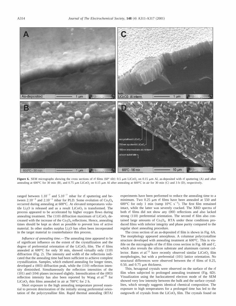
Figure 9. Three-dimensional AFM representation of the surface of the rf film~left! and the PLD film~right! after annealing at 600°C for 30 min.
-
the
hethar
n oon
anL
the
t.edan
ure
-LDm-
o thel-thee
ing
r-
10.ovepro-allon-by
umstrate-w-
FMf the
crystallites switched to~220! with annealing treatment. This orientation change was not observed in the absence of the LiCoO2 film.The extreme decrease of the~111! aluminum reflection at 38.5° isrecognizable in Fig. 4. The rise of the Al~220! reflection~located at65.1°! is less apparent in this figure due to its lower intensity anddominance of the~110! reflection of LiCoO2. The presence ofLiCoO2 apparently determined the final crystal orientation of taluminum layer, while the boundary between the aluminum andtransition metal oxide remained sharp and straight and appeunaffected on the TEM photograph.
To examine the consistency of the preferred lattice orientatiothe PLD and rf films toward each other, a PLD film was grownan rf-sputtered seed layer of 0.1mm LiCoO2 ~annealed at 600°C, 30min!. As a reference, PLD was simultaneously performed on a blsilicon substrate. This reference sample revealed the typical Pfilm diffraction pattern, indicating~00l! lattice plane orientation. ThePLD film deposited on the seed layer, which exhibited only
Figure 10. RBS spectrum of 0.75mm rf-sputtered LiCoO2 film on siliconsubstrate annealed at 600°C for 30 min.
eed
f
kD
~110! reflection before PLD, showed distinct~006! and ~0012! re-flections, but the~003! and~009! reflections were completely absenThis result indicates that the film structure is not entirely determinby the deposition technique. The distinctive diffraction pattern cbe explained by assuming complete cationic disorder.13 A randomdistribution of the lithium and cobalt atoms would lead to a structsimilar to that of NaCl. Hence, the~003! and ~009! reflections be-come extinct.
Atomic force microscopy (AFM).—Figure 9 shows the threedimensional representation of the surface of the rf film and the Pfilm. Both samples consisted of films of equal thickness and coparable history~annealed at 600°C for 30 min!. The rf film exhibitedcoarser grains and increased surface roughness compared tPLD film. The LiCoO2 lattice growth during deposition and anneaing treatment is not isotropic. Apparently the growth rate of both~110! oriented rf film, whosec axis was parallel to the film surfacand the~003! oriented PLD film with itsc axis normal to the filmsurface, was larger along thea axis. This is in agreement with theobserved outgrowth of crystals on the surface of rf films durprolonged annealing at elevated temperatures.
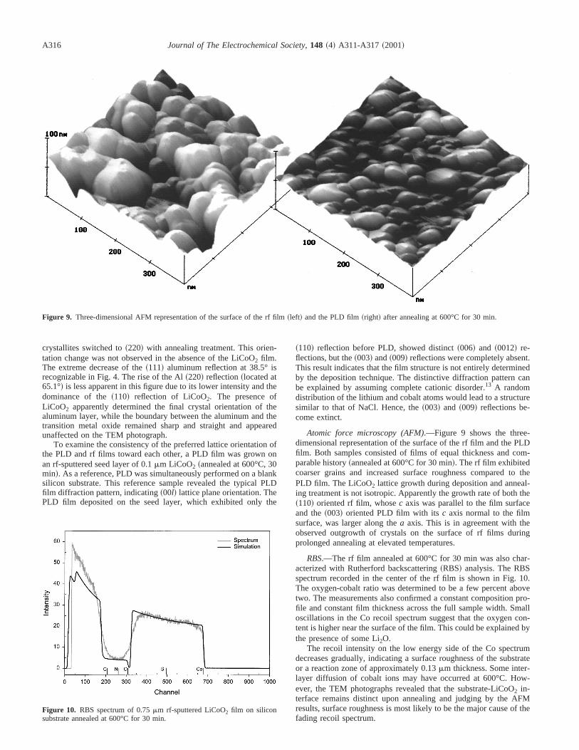
RBS.—The rf film annealed at 600°C for 30 min was also chaacterized with Rutherford backscattering~RBS! analysis. The RBSspectrum recorded in the center of the rf film is shown in Fig.The oxygen-cobalt ratio was determined to be a few percent abtwo. The measurements also confirmed a constant compositionfile and constant film thickness across the full sample width. Smoscillations in the Co recoil spectrum suggest that the oxygen ctent is higher near the surface of the film. This could be explainedthe presence of some Li2O.
The recoil intensity on the low energy side of the Co spectrdecreases gradually, indicating a surface roughness of the subor a reaction zone of approximately 0.13mm thickness. Some interlayer diffusion of cobalt ions may have occurred at 600°C. Hoever, the TEM photographs revealed that the substrate-LiCoO2 in-terface remains distinct upon annealing and judging by the Aresults, surface roughness is most likely to be the major cause ofading recoil spectrum.

terel
d,x-r-ubvidos
oner-histhforanouese
tics-
r aail-
L. H.M
nts,S
this
n,
. A.
Journal of The Electrochemical Society, 148 ~4! A311-A317 ~2001! A317
Conclusions
The preparation of preferentially oriented, submicromeLiCoO2 films has been achieved. The deposition technique largdetermined the LiCoO2 unit cell alignment with the substrate anthus, the preferential orientation of the film. RF and PLD films ehibited ~110! and ~003! lattice planes parallel to the substrate suface, respectively. Deposition at 300°C on pre-etched silicon sstrates and subsequent short annealing treatment at 600°C prouniform film texture. Prolonged annealing treatment resulted in lof LiCoO2 and degradation of the preferential orientation.
This research has shown that LiCoO2 films with well-definedgeometry and structure can be prepared using materials commthe integrated circuit industry. A material interaction at the intfaces between the layers of the stack has been observed, but tconsidered beneficial since it contributed to the adhesion strengthe LiCoO2 film to the substrate. Thus these films are suitablefundamental research on electrochemical lithium intercalationhave a prospect for application in microbatteries. The favorableward orientation of the lithium diffusion plane, which is only thcase for the~110! oriented rf films and the high surface area of thefilms could lead to excellent intercalation electrode characterisA full report on the electrochemical properties will follow in a future publication.
Acknowledgments
The authors are indebted to Philips Research Laboratory fotechnical support on sample preparation and characterizationFOM for financial support. Special thanks are due to J. F. M. C
y
-eds
to
isof
dt-
.
llnd
lessen for the operation and assistance on the PLD equipment,G. J. Segeren for the AFM experiments, H. Koster for the SEanalysis; the Philips CFT department for the XRD measuremeM. A. Verheijen for TEM analysis, and Y. Tamminga for the RBmeasurements.
The University of Twente assisted in meeting the publication costs ofarticle.
References
1. M. M. Tackeray, J. O. Thomas, and M. S. Whittingham,Mater. Res. Bull.,42 , 39~March 2000!.
2. Y. Gao and J. R. Dahn,J. Electrochem. Soc.,143, 1783~1996!.3. P. Fragnaud, T. Brousse, and D. M. Sleich,J. Power Sources63, 187 ~1996!.4. D. Morrison,Electronic Design, 47~26!, 63 ~1999!.5. R. E. van de Leest and F. Roozeboom,Mater. Res. Soc. Symp. Proc.,525, 351
~1998!.6. R. Alcantara, P. Lavela, J. L. Tirado, E. Zhecheva, and R. Stoyanova,J. Solid State
Electrochem.,3, 121 ~1999!.7. R. J. Gummow, D. C. Liles, and M. M. Tackeray,Mater. Res. Bull.,28, 235
~1993!.8. G. G. Amatucci, J. M. Tarascon, D. Larcher, and L. C. Klein,Solid State Ionics,
84, 169 ~1997!.9. M. Antaya, J. R. Dahn, J. S. Preston, E. Rossen, and J. N. Reimers,J. Electrochem.
Soc.,140, 575 ~1993!.10. B. Wang, J. B. Bates, F. X. Hart, B. C. Sales, R. A. Zuhr, and J. D. RobertsoJ.
Electrochem. Soc.,143, 3203~1996!.11. J. B. Bates, N. J. Dudney, B. J. Neudecker, F. X. Hart, H. P. Jun, and S
Hackney,J. Electrochem. Soc.,147, 59 ~2000!.12. J. K. Lee, S. J. Lee, H. K. Baik, H. Y. Lee, S. W. Jang, S. M. Lee,Electrochem.
Solid-State Lett.,2, 512 ~1999!.13. H. W. Wang, Y. I. Jang, B. Huang, D. R. Sadoway, and Y. M. Chiang,J. Electro-
chem. Soc.,146, 473 ~1999!.