Unusual role of epilayer–substrate interactions in determining ...
6
Unusual role of epilayer–substrate interactions in determining orientational relations in van der Waals epitaxy Lei Liu a,1 , David A. Siegel b,1 , Wei Chen c,d,1 , Peizhi Liu a,e , Junjie Guo e,f , Gerd Duscher e,f , Chong Zhao g,h , Hao Wang g,h , Wenlong Wang h , Xuedong Bai h , Kevin F. McCarty b , Zhenyu Zhang c,2 , and Gong Gu a,2 a Department of Electrical Engineering and Computer Science, University of Tennessee, Knoxville, TN 37996; b Materials Physics Department, Sandia National Laboratories, Livermore, CA 94550; c International Center for Quantum Design of Functional Materials, Hefei National Laboratory for Physical Sciences at the Microscale, and Synergetic Innovation Center of Quantum Information and Quantum Physics, University of Science and Technology of China, Hefei 230026, China; d Department of Physics, The University of Tennessee, Knoxville, TN 37996; e Department of Materials Science and Engineering, University of Tennessee, Knoxville, TN 37996; f Materials Science and Technology Division, Oak Ridge National Laboratory, Oak Ridge, TN 37831; g International Center for Quantum Materials, School of Physics, Peking University, Beijing 100871, China; and h Beijing National Laboratory for Condensed Matter Physics, Institute of Physics, Chinese Academy of Sciences, Beijing 100190, China Edited by Paul L. McEuen, Cornell University, Ithaca, NY, and approved October 22, 2014 (received for review April 6, 2014) Using selected-area low-energy electron diffraction analysis, we showed strict orientational alignment of monolayer hexagonal boron nitride (h-BN) crystallites with Cu(100) surface lattices of Cu foil substrates during atmospheric pressure chemical vapor deposition. In sharp contrast, the graphene–Cu(100) system is well-known to assume a wide range of rotations despite graphene’s crystallographic similar- ity to h-BN. Our density functional theory calculations uncovered the origin of this surprising difference: The crystallite orientation is deter- mined during nucleation by interactions between the cluster’s edges and the substrate. Unlike the weaker B– and N–Cu interactions, strong C–Cu interactions rearrange surface Cu atoms, resulting in the aligned geometry not being a distinct minimum in total energy. The discovery made in this specific case runs counter to the conventional wisdom that strong epilayer– substrate interactions enhance orientational align- ment in epitaxy and sheds light on the factors that determine orienta- tional relation in van der Waals epitaxy of 2D materials. two-dimensional materials | van der Waals epitaxy | hexagonal boron nitride | graphene | orientational relation R esearch on van der Waals (vdW) heterostructures formed by stacking up various 2D crystals is an emerging field (1) be- cause the numerous possible interfaces may lead to new physics not necessarily associated with the constituent 2D materials and, therefore, to novel applications. Most pioneering works on vdW heterostructures are based on mechanical placement of exfoli- ated 2D crystal flakes (2–4), where uncertainty in the orienta- tional relation between layers is inevitable. For some purposes, e.g., to enhance graphene’s transport by placing it on hexagonal boron nitride (3) (h-BN, or simply BN hereafter), the orienta- tional relation is not important. In other cases, however, a de- finitive orientational relation is necessary for certain physical properties to arise. Examples include the tunneling behavior of a graphene–insulator–graphene junction (5) and the band struc- ture of graphene placed on top of BN (2). The only practical way to achieve certainty in orientational relation, or azimuthal order, in vdW heterostructures is epitaxial growth. Actually, vdW epitaxy has been studied for decades as a method to overcome lattice mismatch (6, 7) enabled by the rel- atively weak and flexible vdW interactions between the epilayer and the substrate. Although vdW epitaxy [or quasiepitaxy (8)] is typically incommensurate, there can be a well-defined orienta- tional relation (8), which has been observed in many examples of vdW epitaxy (6, 7, 9–11). In some cases, however, a definitive epilayer–substrate orientational relation is lacking (12, 13). At the moment when vdW epitaxy is shaping into a new thrust area in 2D crystal research, it is imperative to uncover the mecha- nisms that determine the orientational relation. Epilayer–substrate interactions lead to registry in commensu- rate epitaxy, which naturally guarantees orientational alignment between the epilayer and the substrate. In vdW epitaxy, one would intuitively expect that strong epilayer–substrate inter- actions enhance azimuthal order, and this trend has been ob- served in some experiments (14–16). Here we show by a case study that the conventional wisdom does not always apply and that the relationship between the azimuthal order and the epi- layer–substrate interactions in vdW epitaxy is highly case-spe- cific. This surprising finding sheds light on the determination of orientational relation in vdW epitaxy. One would also intuitively expect crystallography and symmetry similarities between the epilayer and substrate to be important, if not determining, factors to orientational alignment. Graphene has been grown with orientational alignment on crystallographi- cally similar BN (10, 11). Lattice constant mismatched transition metal chalcogenides are orientationally aligned to each other in vdW epitaxial heterostructures (7), presumably because they share a threefold symmetry. In this work, we show that threefold symmetric BN exhibits definitive orientational alignments when grown on the fourfold symmetric Cu(100) surface. In stark con- trast, the graphene–Cu(100) epitaxy exhibits a distribution of rotations (17–19). This difference occurs despite the close Significance van der Waals (vdW) heterostructures of dissimilar 2D material sheets held together by vdW interactions promise new physics and applications not necessarily associated with the constituent 2D materials. Only epitaxial growth can achieve the orienta- tional alignment in vdW heterostructures needed to obtain certain novel phenomena. As a case study of vdW epitaxy, we experimentally find that hexagonal boron nitride strictly aligns to Cu(100), whereas crystallographically similar graphene is known to exhibit a wide spread of in-plane rotations. Theoret- ical investigation reveals that this stark difference occurs be- cause the C–Cu interactions are stronger than the B–Cu and N–Cu interactions. This counterintuitive discovery sheds light on ori- entational relationships in vdW epitaxy and their case specificity. Author contributions: L.L. and G.G. designed research; L.L., D.A.S., and K.F.M. performed experiments; W.C. performed computations; L.L., D.A.S., W.C., P.L., J.G., G.D., C.Z., H.W., W.W., X.B., and K.F.M. contributed new reagents/analytic tools; L.L., D.A.S., W.C., K.F.M., Z.Z., and G.G. analyzed data; and L.L., D.A.S., W.C., K.F.M., Z.Z., and G.G. wrote the paper. The authors declare no conflict of interest. This article is a PNAS Direct Submission. 1 L.L., D.A.S., and W.C. contributed equally to this work. 2 To whom correspondence may be addressed. Email: [email protected] or [email protected]. This article contains supporting information online at www.pnas.org/lookup/suppl/doi:10. 1073/pnas.1405613111/-/DCSupplemental. 16670–16675 | PNAS | November 25, 2014 | vol. 111 | no. 47 www.pnas.org/cgi/doi/10.1073/pnas.1405613111
Transcript of Unusual role of epilayer–substrate interactions in determining ...

Unusual role of epilayer–substrate interactions indetermining orientational relations in van derWaals epitaxyLei Liua,1, David A. Siegelb,1, Wei Chenc,d,1, Peizhi Liua,e, Junjie Guoe,f, Gerd Duschere,f, Chong Zhaog,h, Hao Wangg,h,Wenlong Wangh, Xuedong Baih, Kevin F. McCartyb, Zhenyu Zhangc,2, and Gong Gua,2
aDepartment of Electrical Engineering and Computer Science, University of Tennessee, Knoxville, TN 37996; bMaterials Physics Department, Sandia NationalLaboratories, Livermore, CA 94550; cInternational Center for Quantum Design of Functional Materials, Hefei National Laboratory for Physical Sciences atthe Microscale, and Synergetic Innovation Center of Quantum Information and Quantum Physics, University of Science and Technology of China, Hefei230026, China; dDepartment of Physics, The University of Tennessee, Knoxville, TN 37996; eDepartment of Materials Science and Engineering, Universityof Tennessee, Knoxville, TN 37996; fMaterials Science and Technology Division, Oak Ridge National Laboratory, Oak Ridge, TN 37831; gInternational Centerfor Quantum Materials, School of Physics, Peking University, Beijing 100871, China; and hBeijing National Laboratory for Condensed Matter Physics, Instituteof Physics, Chinese Academy of Sciences, Beijing 100190, China
Edited by Paul L. McEuen, Cornell University, Ithaca, NY, and approved October 22, 2014 (received for review April 6, 2014)
Using selected-area low-energy electron diffraction analysis, weshowed strict orientational alignment of monolayer hexagonalboron nitride (h-BN) crystallites with Cu(100) surface lattices of Cu foilsubstrates during atmospheric pressure chemical vapor deposition. Insharp contrast, the graphene–Cu(100) system is well-known to assumea wide range of rotations despite graphene’s crystallographic similar-ity to h-BN. Our density functional theory calculations uncovered theorigin of this surprising difference: The crystallite orientation is deter-mined during nucleation by interactions between the cluster’s edgesand the substrate. Unlike the weaker B– and N–Cu interactions, strongC–Cu interactions rearrange surface Cu atoms, resulting in the alignedgeometry not being a distinct minimum in total energy. The discoverymade in this specific case runs counter to the conventional wisdomthat strong epilayer–substrate interactions enhance orientational align-ment in epitaxy and sheds light on the factors that determine orienta-tional relation in van der Waals epitaxy of 2D materials.
two-dimensional materials | van der Waals epitaxy |hexagonal boron nitride | graphene | orientational relation
Research on van der Waals (vdW) heterostructures formed bystacking up various 2D crystals is an emerging field (1) be-
cause the numerous possible interfaces may lead to new physicsnot necessarily associated with the constituent 2D materials and,therefore, to novel applications. Most pioneering works on vdWheterostructures are based on mechanical placement of exfoli-ated 2D crystal flakes (2–4), where uncertainty in the orienta-tional relation between layers is inevitable. For some purposes,e.g., to enhance graphene’s transport by placing it on hexagonalboron nitride (3) (h-BN, or simply BN hereafter), the orienta-tional relation is not important. In other cases, however, a de-finitive orientational relation is necessary for certain physicalproperties to arise. Examples include the tunneling behavior ofa graphene–insulator–graphene junction (5) and the band struc-ture of graphene placed on top of BN (2).The only practical way to achieve certainty in orientational
relation, or azimuthal order, in vdW heterostructures is epitaxialgrowth. Actually, vdW epitaxy has been studied for decades as amethod to overcome lattice mismatch (6, 7) enabled by the rel-atively weak and flexible vdW interactions between the epilayerand the substrate. Although vdW epitaxy [or quasiepitaxy (8)] istypically incommensurate, there can be a well-defined orienta-tional relation (8), which has been observed in many examples ofvdW epitaxy (6, 7, 9–11). In some cases, however, a definitiveepilayer–substrate orientational relation is lacking (12, 13). Atthe moment when vdW epitaxy is shaping into a new thrust areain 2D crystal research, it is imperative to uncover the mecha-nisms that determine the orientational relation.
Epilayer–substrate interactions lead to registry in commensu-rate epitaxy, which naturally guarantees orientational alignmentbetween the epilayer and the substrate. In vdW epitaxy, onewould intuitively expect that strong epilayer–substrate inter-actions enhance azimuthal order, and this trend has been ob-served in some experiments (14–16). Here we show by a casestudy that the conventional wisdom does not always apply andthat the relationship between the azimuthal order and the epi-layer–substrate interactions in vdW epitaxy is highly case-spe-cific. This surprising finding sheds light on the determination oforientational relation in vdW epitaxy.One would also intuitively expect crystallography and symmetry
similarities between the epilayer and substrate to be important, ifnot determining, factors to orientational alignment. Graphenehas been grown with orientational alignment on crystallographi-cally similar BN (10, 11). Lattice constant mismatched transitionmetal chalcogenides are orientationally aligned to each other invdW epitaxial heterostructures (7), presumably because theyshare a threefold symmetry. In this work, we show that threefoldsymmetric BN exhibits definitive orientational alignments whengrown on the fourfold symmetric Cu(100) surface. In stark con-trast, the graphene–Cu(100) epitaxy exhibits a distribution ofrotations (17–19). This difference occurs despite the close
Significance
van der Waals (vdW) heterostructures of dissimilar 2D materialsheets held together by vdW interactions promise new physicsand applications not necessarily associated with the constituent2D materials. Only epitaxial growth can achieve the orienta-tional alignment in vdW heterostructures needed to obtaincertain novel phenomena. As a case study of vdW epitaxy, weexperimentally find that hexagonal boron nitride strictly alignsto Cu(100), whereas crystallographically similar graphene isknown to exhibit a wide spread of in-plane rotations. Theoret-ical investigation reveals that this stark difference occurs be-cause the C–Cu interactions are stronger than the B–Cu and N–Cuinteractions. This counterintuitive discovery sheds light on ori-entational relationships in vdW epitaxy and their case specificity.
Author contributions: L.L. and G.G. designed research; L.L., D.A.S., and K.F.M. performedexperiments; W.C. performed computations; L.L., D.A.S., W.C., P.L., J.G., G.D., C.Z., H.W.,W.W., X.B., and K.F.M. contributed new reagents/analytic tools; L.L., D.A.S., W.C., K.F.M.,Z.Z., and G.G. analyzed data; and L.L., D.A.S., W.C., K.F.M., Z.Z., and G.G. wrote the paper.
The authors declare no conflict of interest.
This article is a PNAS Direct Submission.1L.L., D.A.S., and W.C. contributed equally to this work.2To whom correspondence may be addressed. Email: [email protected] or [email protected].
This article contains supporting information online at www.pnas.org/lookup/suppl/doi:10.1073/pnas.1405613111/-/DCSupplemental.
16670–16675 | PNAS | November 25, 2014 | vol. 111 | no. 47 www.pnas.org/cgi/doi/10.1073/pnas.1405613111

crystallographic similarity between graphene and BN. First-prin-ciples calculations reveal that the difference between the twosystems arises from epilayer–substrate interactions.
ResultsMonolayer BN Single-Crystal Growth. Methods describes the growthby atmospheric-pressure chemical vapor deposition (APCVD) (20)on cold-rolled copper foils. Except for the precursor, the conditionswere the same as we previously used to grow graphene crystallites(19). The wide thermal decomposition window and the violent de-composition behavior of the precursor ammonia borane (H3B−NH3)hinder the synthesis of monolayer BN crystallites with well-defined,energetically favored edges (21, 22). We leverage the diffusion-limited kinetics of APCVD to achieve a low feedstock arrival rate,which was further controlled by the precursor charge. Analogousto graphene APCVD using highly diluted methane (23, 24), themethod results in monolayer single crystals with energetically favorededges, commonly believed to be nitrogen-terminated zigzag edges,and therefore exhibiting the distinctive equilateral triangle shape (22,25). The scanning electron microscopy (SEM) image in Fig. 1Ashows isolated, equilateral triangle-shaped BN domains grown witha low precursor charge. With increased precursor charge, crystallitescoalesce into islands of complex shapes, such as butterflies and stars(Fig. 1B and SI Appendix, Fig. S1). Arrows overlaid on the BNdomains in Fig. 1A suggest that these triangles are oriented only inseveral directions, a result that warrants an in-depth investigation.In addition, samples were characterized by X-ray photoemis-
sion spectroscopy and UV-visible spectroscopy (SI Appendix, Figs.S2 and S3) for chemical analysis and optical band-gap measure-ment, respectively. On the atomic scale, the element-contrast(Z-contrast) annular dark-field scanning transmission electronmicroscopy (ADF STEM) image and the corresponding intensityline profile (Fig. 1 C and D) show clear distinction between in-dividual B and N atoms, which, considering the stacking of bulkhexagonal boron nitride (26), unambiguously confirm that thecrystallites are monolayer.
Monolayer BN–Cu(100) Superstructure. To understand the limitednumber of allowed orientations of the BN crystallites suggestedby Fig. 1A, low-energy electron microscopy (LEEM) and selected-area low-energy electron diffraction (μ-LEED) were performed todetermine the relative crystallography of the BN domains on theCu foil substrate. Every diffraction pattern acquired across milli-meter length scales of the surface indicated a Cu(100) surfacetermination, consistent with the fact that the cold-rolled Cu foilsurface after thermal annealing consists nearly exclusively of large,(100)-oriented grains (17, 27, 28). Fig. 2A displays a representativeμ-LEED pattern of a BN island, showing diffraction spots corre-sponding to Cu(100), BN, and a moiré formed between the BN andthe underlying Cu(100). Because this pattern is rather complicated,we illustrate it schematically in Fig. 2B. The four first-order dif-fraction spots of the Cu(100) surface lattice are marked by brownarrows in Fig. 2A and are colored brown in Fig. 2B. Similarly, thesix first-order diffraction spots corresponding to the BN overlayerare marked in blue. The moiré spots are circled and colored ingreen, and we note that many of the circles in Fig. 2A contain twoor three diffraction spots; these are represented by single greendots in Fig. 2B. The BN island exhibits only one set of diffractionspots, which confirms its monocrystallinity. At the selected electronenergy, the pattern in Fig. 2A shows a clear threefold symmetry:higher and lower intensity BN spots are marked by thicker andthinner blue arrows, respectively.To account for the moiré pattern, we first note that the overall
diffraction pattern has two high-symmetry directions: a horizontaldirection with many closely spaced diffraction peaks from thesuperstructure (moiré) and a vertical direction where the separa-tion between rows of closely spaced superstructure peaks is the Cu(100) reciprocal lattice constant. In the vertical direction, thevertical components of the BN and Cu(100) reciprocal latticesroughly align, i.e., aCu* ∼ aBN*sin60°, where aCu* and aBN* are thereciprocal lattice constants of the BN and the Cu(100) 2D lattices,respectively, leading to each Cu spot being collinear with a pair offirst-order BN spots (blue). The close match between the BN andCu(100) real-space lattice constants (aCu ∼ aBN ∼ 0.25 nm) andthe relationships aCu* = 2π/aCu and aBN* = 4π/(
ffiffiffiffi
3p
aBN) explainthis coincidence. In the horizontal direction, the ratio of theCu(100) to BN reciprocal lattice constants is very close to 5:6, whichleads to a supercell that in real space is 5× the Cu unit cell or 6× theBN unit cell. In reciprocal space this match creates four moiré spots(marked by green circles) equally spaced at 1/5 the separation be-tween the (00) spot and the first-order Cu spot, or five diffractionspots (including the first-order Cu spot) spaced at 1/6 the separationbetween the (00) beam and the first-order BN spot.An atomic model (Fig. 2C) is constructed based on these coinci-
dences observed in the diffraction pattern: aCu ∼ aBN (within +2.1%)along the vertical direction, and 5aCu ∼ 6aBNsin60° (within –1.8%)in the horizontal direction. We point out that this model is an il-lustration of the orientational relation and periodicity; any lateraltranslation is allowable. As a consequence of small lattice mismatches(+2.1% and –1.8% in the two directions), each moiré spot marked bya green circle in Fig. 2A actually comprises three closely spaced spots.
Orientational Alignment Between BN Crystallites and the Cu(100)Lattice. Unlike the graphene–Cu(100) system (17–19), μ-LEEDanalysis on multiple BN crystallites surprisingly shows that onlyfour equivalent orientations occur for BN on Cu(100), i.e., BNcrystallites are well aligned to the underlying Cu(100) lattice. Fig.3A shows a bright-field LEEM image, where BN islands are im-aged as bright triangular regions. The entire field of view is a singleCu(100) grain. Fig. 3 C–F displays μ-LEED patterns acquired onfour BN islands that are circled and labeled in Fig. 3A. These fourdiffraction patterns correspond to four orientations of the BN onthe Cu(100) surface. In each pattern, one BN reciprocal primitivevector aligns with one reciprocal primitive vector of the Cu(100)surface. Thus, by symmetry there are four equivalent orientationsof BN crystals on Cu (100). Furthermore, dark-field imaging (SIAppendix, Fig. S5) of the same region imaged in Fig. 3 shows thatfour and only four orientations account for all of the BN islands in
Fig. 1. Monolayer BN crystals obtained by APCVD. (A and B) RepresentativeSEM images of BN crystals on Cu foils with different film coverages. Spatiallyisolated equilateral triangles (A) and complex structures (B) are achieved bycontrolling the amount of precursor. Red arrows in A indicate orientations ofcrystallites. (C) Z-contrast ADF-STEM image of a BN crystallite, showing single-layer character. Pink and blue circles denote B and N atoms, respectively. (D)Intensity profile along the green line in C, identifying B and N atoms.
Liu et al. PNAS | November 25, 2014 | vol. 111 | no. 47 | 16671
APP
LIED
PHYS
ICAL
SCIENCE
S

the entire field of view. Fig. 3B schematically illustrates the fourequivalent BN orientations in real space.In addition, another set of LEEM–LEED data (SI Appendix,
Fig. S4), with only the first-order Cu and BN diffraction spotsvisible, more simply documents the epitaxial relationships revealedin Fig. 3. Moreover, a better-resolved bright-field image (SI Ap-pendix, Fig. S4A), which reveals the equilateral triangle shape ofthe BN crystallites, together with the diffraction patterns allows usto confirm that the edge orientations of the BN triangles are in-deed zigzag. (In Fig. 3A the crystallites are incompletely imaged,possibly due to the nonplanarity of the Cu foil.)With the four allowed orientations accurately identified by
LEEM and μ-LEED, SEM provides statistics over large areas. Fig.4A shows a representative SEM image of BN islands grown on anas-received Cu foil. The orientations of triangular crystallites arecarefully examined and analyzed, exploiting the distinctive equilat-eral triangle shape and the fact that their sides are zigzag edges.Four and only four possible orientations are observed, in goodagreement with the LEEM–LEED measurement, as well as anearlier phenomenological observation (28) that the triangulardomains tended to have one orientation. The uneven distributionbetween the orientations shown in the histogram (Fig. 4C) may bedue to the vicinal surface of the Cu grain. Interestingly, on elec-trochemically polished foils (Fig. 4 B and D) one orientation dom-inates, perhaps because the polishing resulted in a surface whosesteps and terraces were preferentially aligned along one direction.
Oxygen Impurity Induced Misalignment. To test the sensitivity ofthe BN–Cu(100) orientational relation to the BN–Cu(100) inter-actions, we grew BN on oxygen-contaminated Cu foils withoutchanging the recipe. Whereas surface oxygen has been associatedwith intriguing effects on graphene island morphology (29, 30),here we focus on its alteration to the cluster–substrate interactions.The LEED pattern (Fig. 5A) acquired from a region free of BNhas four diffraction spots that are not present for a simple Cu(100)surface. These additional spots are attributed to the c(2 × 2) re-construction of Cu(100) caused by adsorbed oxygen (31). We thenplaced the electron beam spot within individual BN islands toperform μ-LEED. Fig. 5B displays a diffraction pattern obtained inone island, showing the Cu, BN, and c(2 × 2) reconstruction spots;some of the BN–Cu(100) moiré spots present in Figs. 2 and 3 arefaintly visible. More important, new moiré spots (circled in cyan)appear, corresponding to double diffraction from the c(2 × 2) andBN lattices. This moiré formed by the BN and the c(2 × 2) pro-vides strong evidence that the oxygen impurity is underneath theBN island. Due to the oxygen, the BN crystallites no longer lockinto the four aligned orientations on Cu(100). The large-areaLEED pattern in Fig. 5C, along with the orientation statistics (SIAppendix, Fig. S6), shows multiple rotation angles on individual
Cu(100) grains. This wide angular distribution, along with the weakBN–Cu moiré spots, indicates that the intercalation of oxygenatoms between the BN crystallite and the Cu substrate alters theinteraction and therefore the alignment between the two lattices,providing strong evidence that the BN–Cu interaction is essentialto achieve the observed alignment of BN on pristine Cu(100).
Density Functional Theory Calculations. To understand why BNrigorously aligns on Cu(100) whereas graphene does not, weperformed a comparative density functional theory (DFT) study tocalculate the total energy vs. rotation angle of BN and grapheneclusters on Cu(100) (Fig. 6), which simulate the initial nucleationstage (32, 33). We used the Vienna ab initio simulation package(34) with the projector augmented wave (PAW) method (35, 36)and the Perdew-Burke-Ernzerhof parameterization of the gener-alized gradient approximation (PBE-GGA) (37), as well as DFT-D2, a semiempirical approach that includes vdW interactions (38,39). The investigated structures were first relaxed using PBE-GGA functionals without vdW interactions to search for stable ormetastable geometries around initial translational positions and
Fig. 2. BN–Cu(100) superstructure. (A) μ-LEED pattern (63 V) obtained on a triangular BN crystallite on a Cu(100) grain. First-order diffraction spots ofCu are marked by brown arrows, and the brighter and dimmer BN spots are marked by thicker and thinner blue arrows, respectively. Reciprocalprimitive vectors of BN and Cu are drawn as blue and brown dashed arrows, respectively. Selected moiré spots are marked by green circles. (B) Schematic ofthe diffraction spots arising from BN and Cu. (C) Atomic model of BN on Cu(100) derived from the diffraction pattern. A superstructure cell, marked by greenarrows, is formed between BN and Cu(100) lattices. The two lattices match well at spacings of 5 Cu cells or 6 BN cells. Lateral registry shown is arbitrary.Primitive vectors of the BN and Cu lattices are also shown.
Fig. 3. Alignment between BN crystallites and Cu(100) surface lattice. (A) LEEMimage (25-V, 15-μm-diameter field of view) of BN islands (bright) on a singleCu(100) grain. White circles denote regions where μ-LEED patterns (C–F) wereobtained. (B) Real-space atomic model of four equivalent orientations of tri-angular BN crystallites on Cu(100). (C–F) μ-LEED patterns acquired at locationsmarked in A. Blue arrows mark the reciprocal primitive vectors of BN. Brownarrows in C mark the first-order diffraction spots of Cu(100). The BN crystals ex-hibit threefold symmetry in the diffraction pattern at the chosen electron energy.
16672 | www.pnas.org/cgi/doi/10.1073/pnas.1405613111 Liu et al.

rotational orientations, followed by DFT-D2 calculations fora second-step relaxation.The relaxed BN cluster exhibits a domed structure, similar to
graphene clusters on Cu(111) and Ir(111) (32, 40), indicatingthat the cluster interacts with the substrate predominantly at theperiphery. Due to the three- and fourfold symmetries of BN andCu(100), respectively, a rotation angle θ = Θ is equivalent to θ =Θ + 30°. Meanwhile, due to reflection symmetry, the total energyEtotal (Θ) = Etotal (−Θ). Therefore, we only need to consider θ ∈[0°, 15°], and thus set the initial rotational angles to be θ = 0°, 5°,10°, and 15°. Fig. 6A shows two of the stable or metastable ge-ometries after relaxation by DFT-D2, θ = 0° and 6.2°. Fig. 6Bdisplays the total energy vs. rotation angle plot for all of thestable–metastable configurations discovered by relaxation usingPBE and DFT-D2. The total energy at θ = 0° was set to zero asthe reference for both methods, which resulted in the sametrend, suggesting that the effect of the net corrections due tovdW interactions between the cluster and the Cu substrate isquite close for all orientations and therefore plays a minimal rolein determining the relative stability. One exception is that the θ =9.1° geometry obtained by PBE relaxed into θ = 6.2° for DFT-D2, probably due to vdW interactions between edge atoms and
Cu atoms underneath. The calculations support the experimen-tally observed alignment between the BN and Cu(100) lattices.The alignment of one edge of the cluster with the substrate lattice(Fig. 6A) substantially enhances the cluster–substrate interaction,and any rotation away from this high-symmetry configuration willmake the cluster less stable.For comparison, we calculated the total energy vs. rotation angle
for a graphene cluster with the same geometry. (Whereas grapheneclusters should be equiangular hexagons, our clusters can be con-sidered as six-sided with three edges of the shortest possible zigzaggeometry.) The results are summarized in Fig. 6 C and D. Withinthe PBE, a few orientations near θ = 6.5° have nearly the sametotal energies as θ = 0°. By adding vdW interactions, some of theseconfigurations even become more stable than θ = 0°. Moreover,other metastable orientations between θ = 0° and 6.5° are verylikely to exist, although the present DFT study did not find any dueto the stringent criteria used for force convergence in ionic re-laxation. Therefore, in contrast with the strict alignment of BN onthe Cu(100), the graphene cluster can rotate away from the high-symmetry orientation θ = 0°, consistent with the previous reportedexperiments (17), where the diffraction intensity is high for θ ∈ [0°,∼6.5°] although nonzero elsewhere.
DiscussionThe calculated narrow rotation angle window of low total energyfor BN–Cu(100) and a much wider one for graphene–Cu(100)are consistent with experiments. Nevertheless, the DFT-obtaineddata points in Fig. 6 per se do not explain why BN–Cu(100)strictly aligns whereas graphene–Cu(100) exhibits nonzero dif-fraction intensity at all angles, because these data points are totalenergy “local minima” in structural relaxation. The question howstable these local minima (i.e., metastable configurations) are inthe two systems might be answered by exploring the rotationbarriers between these local minima at a significantly highercomputational cost than in the present work. Instead, we showbelow that the knowledge of the exact energy landscape betweenthese local minima is not necessary to gain insights into thealignment mechanism.By inspecting the Cu atoms in the top-view models of Fig. 6 A and
C, we see that the graphene cluster induces more Cu atom rear-rangement than does the BN cluster, making the Cu(100) substratemore “reconstructed” at the cluster periphery. (SI Appendix, Fig. S9provides a more graphical illustration of the difference in substratedistortion.) At a growth temperature close to the melting point ofbulk Cu, these Cu atoms are pulled by a rotated cluster from theiroriginal positions in the Cu lattice to maximize cluster-edge–substrate binding and therefore minimize the cluster–substratesystem total energy. A graphene zigzag edge, if away from a Cu<100> direction, induces appreciable rearrangement of surfaceCu atoms, due to strong C–Cu interactions. This action blurs the
Fig. 4. Statistics of BN–Cu(100) rotational orientations. (A and B) Repre-sentative SEM images of BN islands on (A) an unpolished Cu foil and (B) anelectrochemically polished Cu foil. Four possible orientations of BN crystalsare denoted A1, A2, B1, and B2 shown by legends. (C and D) Orientationhistograms of triangular BN crystallites within individual Cu grains. Cu grainboundaries are clearly identifiable in SEM, as delineated by dashed lines in Aand B.
Fig. 5. Oxygen impurity induced misalignment. (A) Selected-area LEED pattern of a BN-free region of an oxygen-contaminated Cu foil, showing Cu(100) (1 ×1) and c(2 × 2) spots, distinguished by brown and red circles, respectively. (B) μ-LEED pattern from a single BN island. The blue circles indicate the first-orderdiffraction spots from BN. Moiré diffraction spots (circled in cyan) due to multiple scattering by a c(2 × 2) and BN reciprocal lattice vectors (as exem-plified by yellow arrows) prove the presence of oxygen impurity underneath the BN. BN–Cu(100) moiré spots are circled in green. (C ) LEED patternwith multiple sets of BN diffraction spots, highlighted by blue circles, which reveal the misalignment of BN grains on the O–Cu(100) surface.
Liu et al. PNAS | November 25, 2014 | vol. 111 | no. 47 | 16673
APP
LIED
PHYS
ICAL
SCIENCE
S
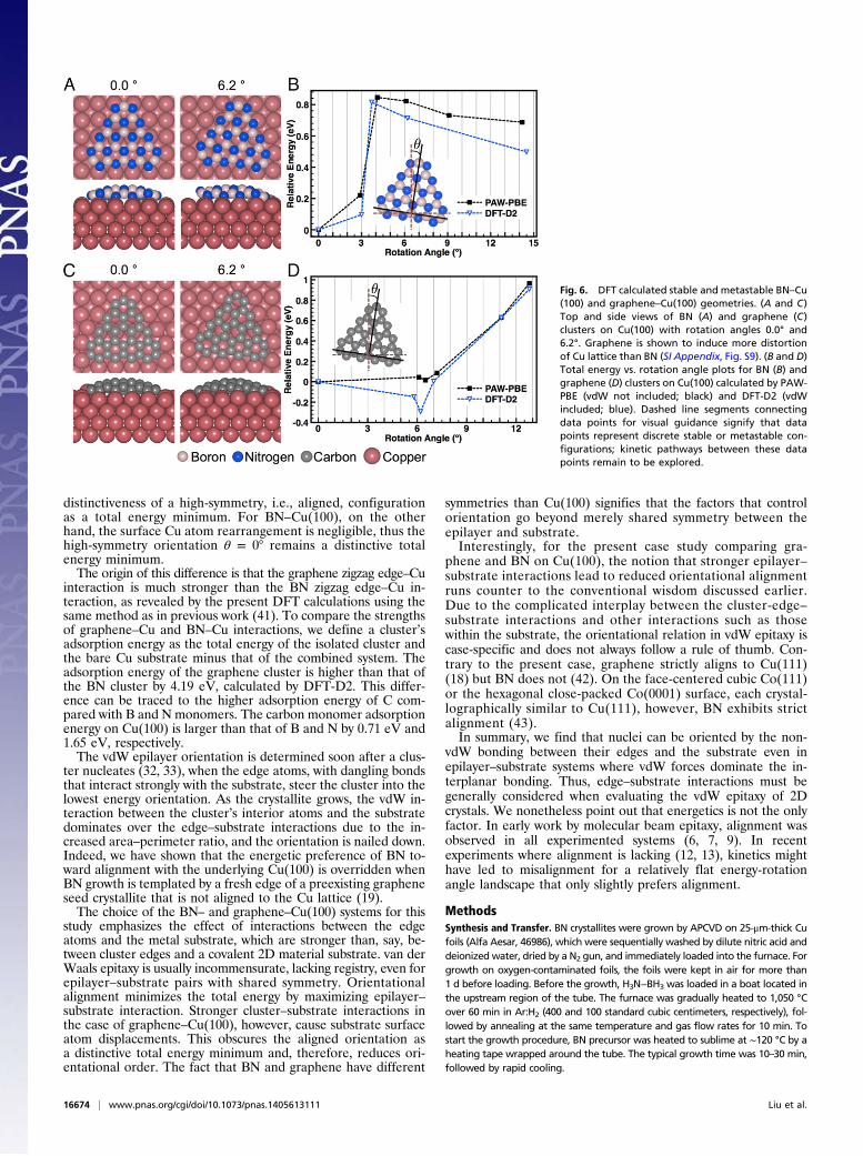
distinctiveness of a high-symmetry, i.e., aligned, configurationas a total energy minimum. For BN–Cu(100), on the otherhand, the surface Cu atom rearrangement is negligible, thus thehigh-symmetry orientation θ = 0° remains a distinctive totalenergy minimum.The origin of this difference is that the graphene zigzag edge–Cu
interaction is much stronger than the BN zigzag edge–Cu in-teraction, as revealed by the present DFT calculations using thesame method as in previous work (41). To compare the strengthsof graphene–Cu and BN–Cu interactions, we define a cluster’sadsorption energy as the total energy of the isolated cluster andthe bare Cu substrate minus that of the combined system. Theadsorption energy of the graphene cluster is higher than that ofthe BN cluster by 4.19 eV, calculated by DFT-D2. This differ-ence can be traced to the higher adsorption energy of C com-pared with B and N monomers. The carbon monomer adsorptionenergy on Cu(100) is larger than that of B and N by 0.71 eV and1.65 eV, respectively.The vdW epilayer orientation is determined soon after a clus-
ter nucleates (32, 33), when the edge atoms, with dangling bondsthat interact strongly with the substrate, steer the cluster into thelowest energy orientation. As the crystallite grows, the vdW in-teraction between the cluster’s interior atoms and the substratedominates over the edge–substrate interactions due to the in-creased area–perimeter ratio, and the orientation is nailed down.Indeed, we have shown that the energetic preference of BN to-ward alignment with the underlying Cu(100) is overridden whenBN growth is templated by a fresh edge of a preexisting grapheneseed crystallite that is not aligned to the Cu lattice (19).The choice of the BN– and graphene–Cu(100) systems for this
study emphasizes the effect of interactions between the edgeatoms and the metal substrate, which are stronger than, say, be-tween cluster edges and a covalent 2D material substrate. van derWaals epitaxy is usually incommensurate, lacking registry, even forepilayer–substrate pairs with shared symmetry. Orientationalalignment minimizes the total energy by maximizing epilayer–substrate interaction. Stronger cluster–substrate interactions inthe case of graphene–Cu(100), however, cause substrate surfaceatom displacements. This obscures the aligned orientation asa distinctive total energy minimum and, therefore, reduces ori-entational order. The fact that BN and graphene have different
symmetries than Cu(100) signifies that the factors that controlorientation go beyond merely shared symmetry between theepilayer and substrate.Interestingly, for the present case study comparing gra-
phene and BN on Cu(100), the notion that stronger epilayer–substrate interactions lead to reduced orientational alignmentruns counter to the conventional wisdom discussed earlier.Due to the complicated interplay between the cluster-edge–substrate interactions and other interactions such as thosewithin the substrate, the orientational relation in vdW epitaxy iscase-specific and does not always follow a rule of thumb. Con-trary to the present case, graphene strictly aligns to Cu(111)(18) but BN does not (42). On the face-centered cubic Co(111)or the hexagonal close-packed Co(0001) surface, each crystal-lographically similar to Cu(111), however, BN exhibits strictalignment (43).In summary, we find that nuclei can be oriented by the non-
vdW bonding between their edges and the substrate even inepilayer–substrate systems where vdW forces dominate the in-terplanar bonding. Thus, edge–substrate interactions must begenerally considered when evaluating the vdW epitaxy of 2Dcrystals. We nonetheless point out that energetics is not the onlyfactor. In early work by molecular beam epitaxy, alignment wasobserved in all experimented systems (6, 7, 9). In recentexperiments where alignment is lacking (12, 13), kinetics mighthave led to misalignment for a relatively flat energy-rotationangle landscape that only slightly prefers alignment.
MethodsSynthesis and Transfer. BN crystallites were grown by APCVD on 25-μm-thick Cufoils (Alfa Aesar, 46986), which were sequentially washed by dilute nitric acid anddeionized water, dried by a N2 gun, and immediately loaded into the furnace. Forgrowth on oxygen-contaminated foils, the foils were kept in air for more than1 d before loading. Before the growth, H3N−BH3 was loaded in a boat located inthe upstream region of the tube. The furnace was gradually heated to 1,050 °Cover 60 min in Ar:H2 (400 and 100 standard cubic centimeters, respectively), fol-lowed by annealing at the same temperature and gas flow rates for 10 min. Tostart the growth procedure, BN precursor was heated to sublime at ∼120 °C by aheating tape wrapped around the tube. The typical growth time was 10–30 min,followed by rapid cooling.
Fig. 6. DFT calculated stable and metastable BN–Cu(100) and graphene–Cu(100) geometries. (A and C)Top and side views of BN (A) and graphene (C)clusters on Cu(100) with rotation angles 0.0° and6.2°. Graphene is shown to induce more distortionof Cu lattice than BN (SI Appendix, Fig. S9). (B and D)Total energy vs. rotation angle plots for BN (B) andgraphene (D) clusters on Cu(100) calculated by PAW-PBE (vdW not included; black) and DFT-D2 (vdWincluded; blue). Dashed line segments connectingdata points for visual guidance signify that datapoints represent discrete stable or metastable con-figurations; kinetic pathways between these datapoints remain to be explored.
16674 | www.pnas.org/cgi/doi/10.1073/pnas.1405613111 Liu et al.

The electrochemical polishing treatment was accomplished in a home-made electrochemical cell using orthophosphoric acid electrolyte and a Cucathode. A 2.0–2.5-V dc voltage was applied for 10–20 min. After polishing,the foils were washed by deionized water and dried by N2.
BN crystallites were transferred onto transmission electron microscope(TEM) grids or other substrates for characterization. To facilitate thetransfer, a thin layer of poly(methyl methacrylate) (PMMA, 2% in anisole)was spin coated on the Cu foil sample (4,000 rpm for 1 min), and the copperwas etched away by floating the foil in a copper etchant (CE-100, Transene).The PMMA–BN membrane was transferred onto the surface of a 10% HClsolution to remove residual metal particles and then washed by deionizedwater several times. Finally, the film was scooped out by the desiredsubstrate (Quantifoil TEM grid with 1.2-μm-diameter holes from Ted Pella,SiO2–Si, or optical quartz plate). The PMMA layer was removed by acetonevapor, followed by thermal annealing (350 °C for 2 h in an Ar:H2
forming gas).
LEEM and LEED Characterizations. Copper foils with APCVD-grown BN do-mains were transferred through air into an Elmitec LEEM III instrument,where they were outgassed in ultrahigh vacuum at about 300 °C. Bright-fieldLEEM images were formed from the specularly reflected (00) beam. Micro-LEED patterns were obtained from areas either 0.5 or 2 μm in diameter.
DFT Calculations. The lattice constant of Cu was obtained via structural opti-mization. Thegeneric Cu(100) surfacewasmodeledbya slabof four atomic layers,and the BN or graphene clusters were placed on top of the metal surfaces. A
vacuum region of more than 11 Å was used to ensure decoupling betweenneighboring slabs. During structural relaxation, the atoms in the bottom twolayers were fixed in their respective bulk positions, with all of the other atomsfully relaxed until the force on any given atomwas smaller than 0.03 eV/Å. A 2 ×2 × 1 k-point mesh was used for a 7 × 7 Cu surface unit cell. The effect of spinpolarization was examined. As a sanity check, we first placed a two-ringBN cluster on Cu(100). The PBE approach led to an unphysical picture,where the cluster stands up on the surface. After the vdW interaction wasincluded, the physically reasonable picture was arrived at (SI Appendix, Fig. S7).Due to the dominance of mostly non-vdW edge–substrate interactions forclusters as depicted in Fig. 6, the accuracy of vdW modeling does not affectour conclusions despite its general importance. Clusters smaller than the onesin Fig. 6 are also examined, and the physical picture of the aligned BN–Cu(100) and rotated graphene on Cu(100) remains (SI Appendix, Fig. S8).
ACKNOWLEDGMENTS. The experimental work was partially supported byNational Science Foundation (ECCS-1231808) and Defense Advanced Re-search Projects Agency. Work at Sandia was supported by the Office of BasicEnergy Sciences, Division of Materials and Engineering Sciences, US Depart-ment of Energy (DOE) under Contract DE-AC04-94AL85000. This research usedresources of Oak Ridge National Laboratory’s Center for Nanophase MaterialsSciences, which is sponsored by the Scientific User Facilities Division, Office ofBasic Energy Sciences, US DOE. The theory work was partially supported byNatural Science Foundation of China (Grants 11034006 and 11204286) andNational Key Basic Research Program of China (Grant 2014CB921103). Thecalculations were performed at National Energy Research Scientific ComputingCenter (NERSC) of the US DOE.
1. Geim AK, Grigorieva IV (2013) Van der Waals heterostructures. Nature 499(7459):419–425.
2. Yankowitz M, et al. (2012) Emergence of superlattice Dirac points in graphene onhexagonal boron nitride. Nat Phys 8(5):382–386.
3. Dean C, et al. (2012) Graphene based heterostructures. Solid State Commun 152(15):1275–1282.
4. Britnell L, et al. (2013) Resonant tunnelling and negative differential conductance ingraphene transistors. Nat Commun 4:1794.
5. Feenstra RM, Jena D, Gu G (2012) Single-particle tunneling in doped graphene-insulator-graphene junctions. J Appl Phys 111(4):043711.
6. Koma A, Saiki K, Sato Y (1989) Heteroepitaxy of a two-dimensional material ona three-dimensional material. Appl Surf Sci 41-42(2):451–456.
7. Koma A (1992) New epitaxial growth method for modulated structures using van derWaals interactions. Surf Sci 267(1-3):29–33.
8. Forrest SR (1997) Ultrathin organic films grown by organic molecular beam depositionand related techiques. Chem Rev 97(6):1793–1896.
9. Koma A (1999) Van der Waals epitaxy for highly lattice-mismatched systems. J CrystalGrowth 201:236–241.
10. Yang W, et al. (2013) Epitaxial growth of single-domain graphene on hexagonalboron nitride. Nat Mater 12(9):792–797.
11. Tang S, et al. (2013) Precisely aligned graphene grown on hexagonal boron nitride bycatalyst free chemical vapor deposition. Sci Rep 3:2666.
12. Shi Y, et al. (2012) van der Waals epitaxy of MoS₂ layers using graphene as growthtemplates. Nano Lett 12(6):2784–2791.
13. Hwang J, et al. (2013) van der Waals epitaxial growth of graphene on sapphire bychemical vapor deposition without a metal catalyst. ACS Nano 7(1):385–395.
14. Preobrajenski AB, Ng ML, Vinogradov AS, Mårtensson N (2008) Controlling graphenecorrugation on lattice-mismatched substrates. Phys Rev B 78(7):073401.
15. Sutter P, Sadowski JT, Sutter E (2009) Graphene on Pt(111): Growth and substrateinteraction. Phys Rev B 80(24):245411.
16. Emtsev KV, Speck F, Seyller T, Ley L, Riley D (2008) Interaction, growth, and orderingof epitaxial graphene on SiC{0001} surfaces: A comparative photoelectron spectros-copy study. Phys Rev B 77(15):155303.
17. Wofford JM, Nie S, McCarty KF, Bartelt NC, Dubon OD (2010) Graphene Islands onCu foils: The interplay between shape, orientation, and defects. Nano Lett 10(12):4890–4896.
18. Ogawa Y, et al. (2012) Domain structure and boundary in single-layer graphenegrown on Cu(111) and Cu(100) films. J Phys Chem Lett 3(2):219–226.
19. Liu L, et al. (2014) Heteroepitaxial growth of two-dimensional hexagonal boron ni-tride templated by graphene edges. Science 343(6167):163–167.
20. Tay RY, et al. (2014) A systematic study of the atmospheric pressure growth of large-area hexagonal crystalline boron nitride film. J Mater Chem C 2(9):1650–1657.
21. Song L, et al. (2010) Large scale growth and characterization of atomic hexagonalboron nitride layers. Nano Lett 10(8):3209–3215.
22. Kim KK, et al. (2012) Synthesis of monolayer hexagonal boron nitride on Cu foil usingchemical vapor deposition. Nano Lett 12(1):161–166.
23. Yu Q, et al. (2011) Control and characterization of individual grains and grain bound-aries in graphene grown by chemical vapour deposition. Nat Mater 10(6):443–449.
24. Vlassiouk I, et al. (2011) Role of hydrogen in chemical vapor deposition growth of
large single-crystal graphene. ACS Nano 5(7):6069–6076.25. Liu Y, Bhowmick S, Yakobson BI (2011) BN white graphene with “colorful” edges: The
energies and morphology. Nano Lett 11(8):3113–3116.26. Geick R, Perry CH (1966) Normal modes in hexagonal boron nitride. Phys Rev 146(2):
543–547.27. Cho J, et al. (2011) Atomic-scale investigation of graphene grown on Cu foil and the
effects of thermal annealing. ACS Nano 5(5):3607–3613.28. Guo N, et al. (2012) Controllable growth of triangular hexagonal boron nitride do-
mains on copper foils by an improved low-pressure chemical vapor deposition
method. Nanotechnology 23(41):415605.29. Hao Y, et al. (2013) The role of surface oxygen in the growth of large single-crystal
graphene on copper. Science 342(6159):720–723.30. Zhou H, et al. (2013) Chemical vapour deposition growth of large single crystals of
monolayer and bilayer graphene. Nat Commun 4:2096.31. Harrison MJ, et al. (2006) Adsorbate-induced surface reconstruction and surface-stress
changes in Cu(100)/O: Experiment and theory. Phys Rev B 74(16):165402.32. Chen W, et al. (2012) Suppression of grain boundaries in graphene growth on su-
perstructured Mn-Cu(111) surface. Phys Rev Lett 109(26):265507.33. Zhang X, Xu Z, Hui L, Xin J, Ding F (2012) How the orientation of graphene is de-
termined during chemical vapor deposition growth. J Phys Chem Lett 3(19):2822–2827.34. Kresse G, Furthmüller J (1996) Efficient iterative schemes for ab initio total-energy
calculations using a plane-wave basis set. Phys Rev B Condens Matter 54(16):
11169–11186.35. Blöchl PE (1994) Projector augmented-wave method. Phys Rev B Condens Matter
50(24):17953–17979.36. Kresse G, Joubert D (1999) From ultrasoft pseudopotentials to the projector aug-
mented-wave method. Phys Rev B 59(3):1758–1775.37. Perdew JP, Burke K, Ernzerhof M (1996) Generalized gradient approximation made
simple. Phys Rev Lett 77(18):3865–3868.38. Grimme S (2006) Semiempirical GGA-type density functional constructed with a long-
range dispersion correction. J Comput Chem 27(15):1787–1799.39. Bucko T, Hafner J, Lebègue S, Ángyán JG (2010) Improved description of the structure
of molecular and layered crystals: Ab initio DFT calculations with van der Waals
corrections. J Phys Chem A 114(43):11814–11824.40. Lacovig P, et al. (2009) Growth of dome-shaped carbon nanoislands on Ir(111): The
intermediate between carbidic clusters and quasi-free-standing graphene. Phys Rev
Lett 103(16):166101.41. Chen H, Zhu W, Zhang Z (2010) Contrasting behavior of carbon nucleation in the
initial stages of graphene epitaxial growth on stepped metal surfaces. Phys Rev Lett
104(18):186101.42. Joshi S, et al. (2012) Boron nitride on Cu(111): An electronically corrugated mono-
layer. Nano Lett 12(11):5821–5828.43. Orofeo CM, Suzuki S, Kageshima H, Hibino H (2013) Growth and low-energy electron
microscopy characterization of monolayer hexagonal boron nitride on epitaxial
cobalt. Nano Res 6(5):335.
Liu et al. PNAS | November 25, 2014 | vol. 111 | no. 47 | 16675
APP
LIED
PHYS
ICAL
SCIENCE
S