Ultra Low Power 1-Bit Full Adder - Information and Library...
34
International Symposium on Devices MEMS, Intelligent Systems & Communication (ISDMISC) 2011 Proceedings published by International Journal of Computer Applications® (IJCA) 9 Ultra Low Power 1-Bit Full Adder Deepa Sinha 1 , Tripti Sharma 2 , K. G. Sharma 3 , Prof. B. P. Singh 4 Department of Electronics and Communication FET-MITS (Deemed University) Lakshmangarh, Rajasthan (INDIA) ABSTRACT In this paper we propose a new 9 transistor 1-bit full adder. The proposed circuit performs efficiently in subthreshold region to employ in ultra low power applications. The main design objective for this new circuit is low power consumption and full voltage swing at a low supply voltage. The proposed cell also remarkably improves the power consumption, power delay product and has better noise immunity when compared to the existing deigns. All simulations are performed on 45nm standard models on Tanned EDA tool version 12.6. General Terms 8T and 9T Keywords Subthreshold region, full adder and low power. 1. INTRODUCTION CMOS VLSI circuits have been evolving into low voltage and low power regimes. In recent years VLSI design space has been focusing on high performance microprocessors. Demand for power sensitive, high speed, small area and low cost designs are increasing every day. This tremendous demand is due to fast growth of battery-operated portable applications such as personal computing devices (portable computers and real time audio and video based multimedia products), wireless communication systems (personal digital assistants and mobile phones), medical applications and other portable devices. Broad acceptance of new applications critically depends on the availability of compact and inexpensive hardware delivering the required high performance and longer battery life.. Unfortunately battery capacity has not improved at the same pace as semiconductor performance and integration and it not expected to improve more than 30% every five years. Consequently, integrated circuits (ICs) designed for hand-held applications must increase performance at reduced energy per computation. Also low power designs reduce cooling cost and increases reliability especially for high density systems. This has pursuit the design engineers to develop a much more flexible design to overcome critical issues of low power consuming, small area and efficient designs. The single-bit full adder is one of the main components in almost all logic structures. The performance of logic structures is highly dependent on the adder cells. The wide use of this operation in arithmetic functions, have made many researchers eager to propose several kinds of different logic styles for implementing 1-bit Full Adder cell, in recent years. To perform arithmetic operation, a device can use up very low power by functioning at very low frequency but it may spend a very long time to finish the operation. The power-delay product can be used for first-level comparison between the different building block designs. One way to achieve ultra low is by running digital circuits in subthreshold mode [1], [2] and [3]. Subthreshold current of an MOSFET transistor occurs when the gate-to-source voltage (V GS ) of a transistor is lower than its threshold voltage (V TH ). When V GS is larger than V TH , majority carriers are repelled from the gate area of the transistor and a minority carrier channel is created. This is known as strong-inversion, as more minority carriers are present in the channel than majority carriers. When V GS is lower than V TH , there are less minority carriers in the channel, but their presence comprises a current and the state is known as weak-inversion. In standard CMOS design, this current is a subthreshold parasitic leakage, but if the supply voltage (VDD) is lowered below V TH, the circuit can be operated using the subthreshold current with ultra-low power consumption. The proposed circuit operates efficiently in subthreshold region to achieve ultra low power. The incentive of operating is able to exploit the sub-threshold leakage current as the operating drive current. Results show improvement in threshold loss, speed and power consumption over the other adders with comparable performance. The special feature of this proposed 9T adder is that it has nearly 10 times improved power consumption than its peer design. The rest of the paper has been organized in four sections. Section II briefly describes the previous work existing. We propose the new design of full adder consisting 9T in Section III. Section IV presents the simulation results and finally, Section V concludes the paper. 2. PRIOR WORK The full adder operation can be stated as follows: Given the three 1-bit inputs A, B, and Cin, it is desired to calculate the two 1-bit outputs Sum and Carry, where Sum = (A xor B) xor Cin Cout = A and B + Cin (A xor B)
Transcript of Ultra Low Power 1-Bit Full Adder - Information and Library...

International Symposium on Devices MEMS, Intelligent Systems & Communication (ISDMISC) 2011 Proceedings published by International Journal of Computer Applications® (IJCA)
9
Ultra Low Power 1-Bit Full Adder Deepa Sinha1, Tripti Sharma2, K. G. Sharma3, Prof. B. P. Singh4
Department of Electronics and Communication FET-MITS (Deemed University)
Lakshmangarh, Rajasthan (INDIA)
ABSTRACT In this paper we propose a new 9 transistor 1-bit full adder. The proposed circuit performs efficiently in subthreshold region to employ in ultra low power applications. The main design objective for this new circuit is low power consumption and full voltage swing at a low supply voltage. The proposed cell also remarkably improves the power consumption, power delay product and has better noise immunity when compared to the existing deigns. All simulations are performed on 45nm standard models on Tanned EDA tool version 12.6.
General Terms
8T and 9T
Keywords Subthreshold region, full adder and low power.
1. INTRODUCTION CMOS VLSI circuits have been evolving into low voltage and low power regimes. In recent years VLSI design space has been focusing on high performance microprocessors. Demand for power sensitive, high speed, small area and low cost designs are increasing every day. This tremendous demand is due to fast growth of battery-operated portable applications such as personal computing devices (portable computers and real time audio and video based multimedia products), wireless communication systems (personal digital assistants and mobile phones), medical applications and other portable devices. Broad acceptance of new applications critically depends on the availability of compact and inexpensive hardware delivering the required high performance and longer battery life.. Unfortunately battery capacity has not improved at the same pace as semiconductor performance and integration and it not expected to improve more than 30% every five years. Consequently, integrated circuits (ICs) designed for hand-held applications must increase performance at reduced energy per computation. Also low power designs reduce cooling cost and increases reliability especially for high density systems. This has pursuit the design engineers to develop a much more flexible design to overcome critical issues of low power consuming, small area and efficient designs.
The single-bit full adder is one of the main components in almost all logic structures. The performance of logic structures is highly dependent on the adder cells. The wide use of this operation in arithmetic functions, have made
many researchers eager to propose several kinds of different logic styles for implementing 1-bit Full Adder cell, in recent years. To perform arithmetic operation, a device can use up very low power by functioning at very low frequency but it may spend a very long time to finish the operation. The power-delay product can be used for first-level comparison between the different building block designs.
One way to achieve ultra low is by running digital circuits in subthreshold mode [1], [2] and [3]. Subthreshold current of an MOSFET transistor occurs when the gate-to-source voltage (VGS) of a transistor is lower than its threshold voltage (VTH). When VGS is larger than VTH, majority carriers are repelled from the gate area of the transistor and a minority carrier channel is created. This is known as strong-inversion, as more minority carriers are present in the channel than majority carriers. When VGS is lower than VTH, there are less minority carriers in the channel, but their presence comprises a current and the state is known as weak-inversion. In standard CMOS design, this current is a subthreshold parasitic leakage, but if the supply voltage (VDD) is lowered below VTH, the circuit can be operated using the subthreshold current with ultra-low power consumption. The proposed circuit operates efficiently in subthreshold region to achieve ultra low power. The incentive of operating is able to exploit the sub-threshold leakage current as the operating drive current. Results show improvement in threshold loss, speed and power consumption over the other adders with comparable performance. The special feature of this proposed 9T adder is that it has nearly 10 times improved power consumption than its peer design. The rest of the paper has been organized in four sections. Section II briefly describes the previous work existing. We propose the new design of full adder consisting 9T in Section III. Section IV presents the simulation results and finally, Section V concludes the paper.
2. PRIOR WORK The full adder operation can be stated as follows: Given the three 1-bit inputs A, B, and Cin, it is desired to calculate the two 1-bit outputs Sum and Carry, where
Sum = (A xor B) xor Cin Cout = A and B + Cin (A xor B)

International Symposium on Devices MEMS, Intelligent Systems & Communication (ISDMISC) 2011 Proceedings published by International Journal of Computer Applications® (IJCA)
10
Fig 1: 1-bit 8T Full Adder
Figure 1 shows the circuit of eight transistor 1-bit full adder cell. The Sum output is basically obtained by a cascaded exclusive ORing [4]-[6] of the three inputs. Cout module is implemented using 2T multiplexer. It is quite evident from Figure 1 that two stage delays are required to obtain the sum output and at most two stage delays are required to obtain the carry output. The voltage drop due to the threshold loss in transistors M3 and M6 in Figure 1 can be minimized by suitably increasing the aspect ratios of the two transistors. However, the threshold voltage drop of |VT p| provided by the PMOS pass transistor M3 when a=0 and b=0 is used to turn on the NMOS pass transistor M8and therefore we get an output voltage equal to |VTp |-VTn, where VTp is the threshold voltage of the PMOS transistor and VTn is the threshold voltage of the NMOS transistor.
Fig 2: In-out waveform of 1-bit 8T Full Adder
Table 1. Performance of 8T and 9T full adder in terms of Threshold loss
A B Cin Sum(8T) Sum(9T) 0 0 0 <<│Vtp│ <<│Vtp│ 0 0 1 1 1 0 1 0 < 30% of logic “1” 1 0 1 1 0 0 1 0 0 < 30% of logic “1” 1 1 0 1 0 0 1 1 0 <<│Vtp│ <<│Vtp│ 1 1 1 1 1
As it can be seen, the 8T full adder Figure 1 is confronted with serious problems especially when Cin=0 and when circuit operates in sub threshold regions. The outputs have good logic level for only a four input vectors. For the remaining input vectors, there is a major degradation in output voltage that may lead to functional failure as well as increased power consumption. As the voltage is scaled down, the signal integrity deteriorates and the speed decreases tremendously.
For input „010‟, output of the first stage XOR gate is complete „1‟. However in the second stage nMOS M4 and pMOS M6 get ON simultaneously. A close loop forms and current feedback through M4 occurs and the output Sum is degraded much less than Vdd (approx. Vdd/2). Similarly for input „100‟, expected Sum should be „1‟ and Cout to be „0‟. But the first stage XOR gate gives a degraded output less than Vdd (approx. Vdd/2). However at higher input voltages (greater than 0.6v) M1 & M3 and M4 & M6 get ON simultaneously. So, there should be minimum loss at first XOR gate, and driving capability of M6 should be high enough than M4. Also for inputs „000‟ and „110‟, output of first XOR gate is „0‟ and when Cin=0, this enables transistors M2 and M3 simultaneously giving a degraded Sum output. Fig.2 shows the input-output waveform of 8T full adder in Figure 1.
3. PROPOSED 9T FULL ADDER DESIGN The circuit shown in Figure 3 is the modified 8T full adder cell using an extra transistor M9 is added to improve the performance of the full adder cell. In the circuit of Fig.1 when inputs are ABCin=000, 010 and 110 then problem persists as two transistors get ON simultaneously at the second stage of XOR and results into the degradation of Sum output due to reduced device resistance as the ON transistors will have combined parallel effect on resistance. This problem is eliminated in the circuit of Fig.3 by adding an extra transistor M9. Now with inputs 010 and 100, the first stage XOR gate gives „1‟ which enables the extra added NMOS M9 giving complete „0‟ and for Cin=0 disable M4. Thus only M6 get ON produce the Sum output eliminating the problem of simultaneous enabling of two transistors and hence the output degradation will be removed. This reduces the threshold loss problem and also improves the speed of the circuit besides giving full swing output. Figure 4 shows the in-out waveform of proposed circuit.
Fig 3: Proposed 1-bit 9T Full Adder
International Symposium on Devices MEMS, Intelligent Systems & Communication (ISDMISC) 2011 Proceedings published by International Journal of Computer Applications® (IJCA)
11
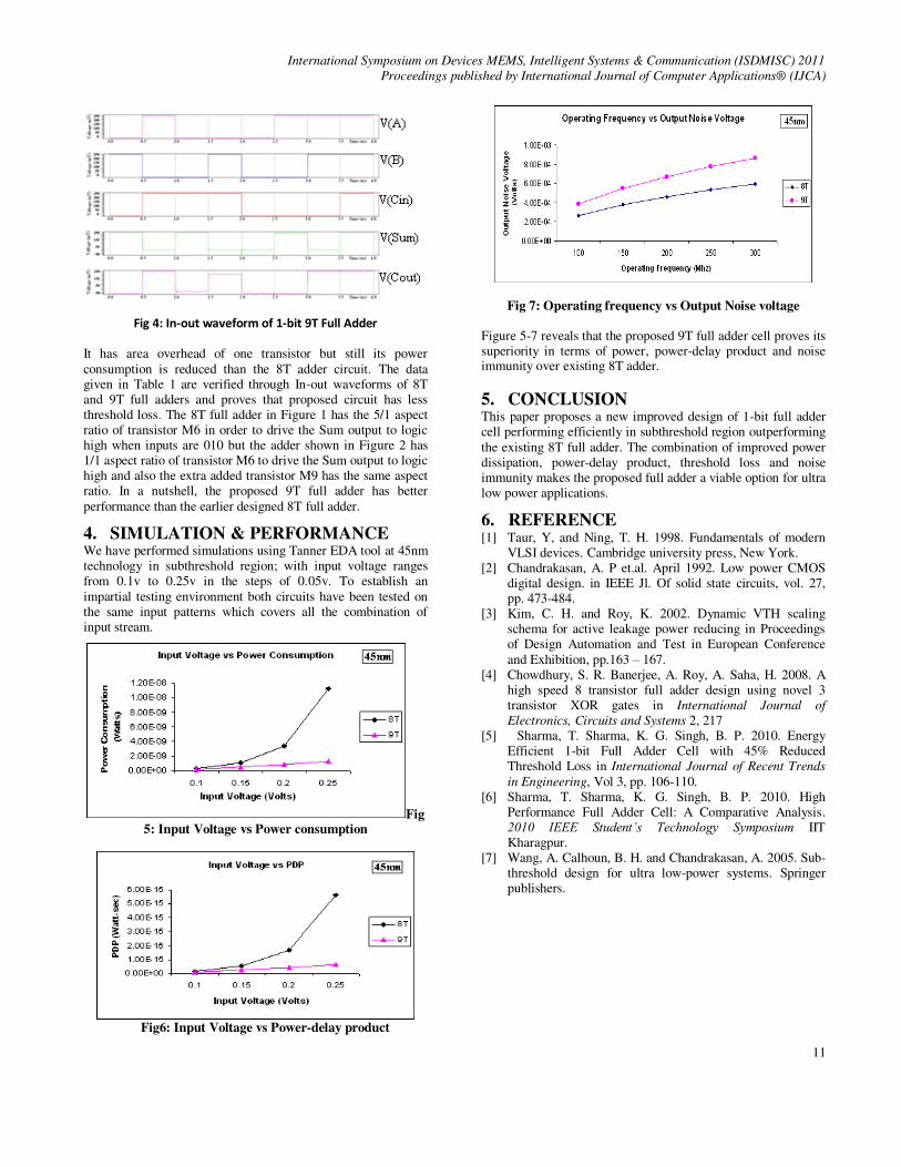
Fig 4: In-out waveform of 1-bit 9T Full Adder
It has area overhead of one transistor but still its power consumption is reduced than the 8T adder circuit. The data given in Table 1 are verified through In-out waveforms of 8T and 9T full adders and proves that proposed circuit has less threshold loss. The 8T full adder in Figure 1 has the 5/1 aspect ratio of transistor M6 in order to drive the Sum output to logic high when inputs are 010 but the adder shown in Figure 2 has 1/1 aspect ratio of transistor M6 to drive the Sum output to logic high and also the extra added transistor M9 has the same aspectratio. In a nutshell, the proposed 9T full adder has better performance than the earlier designed 8T full adder.
4. SIMULATION & PERFORMANCE We have performed simulations using Tanner EDA tool at 45nm technology in subthreshold region; with input voltage rangesfrom 0.1v to 0.25v in the steps of 0.05v. To establish an impartial testing environment both circuits have been tested on the same input patterns which covers all the combination of input stream.
Fig 5: Input Voltage vs Power consumption
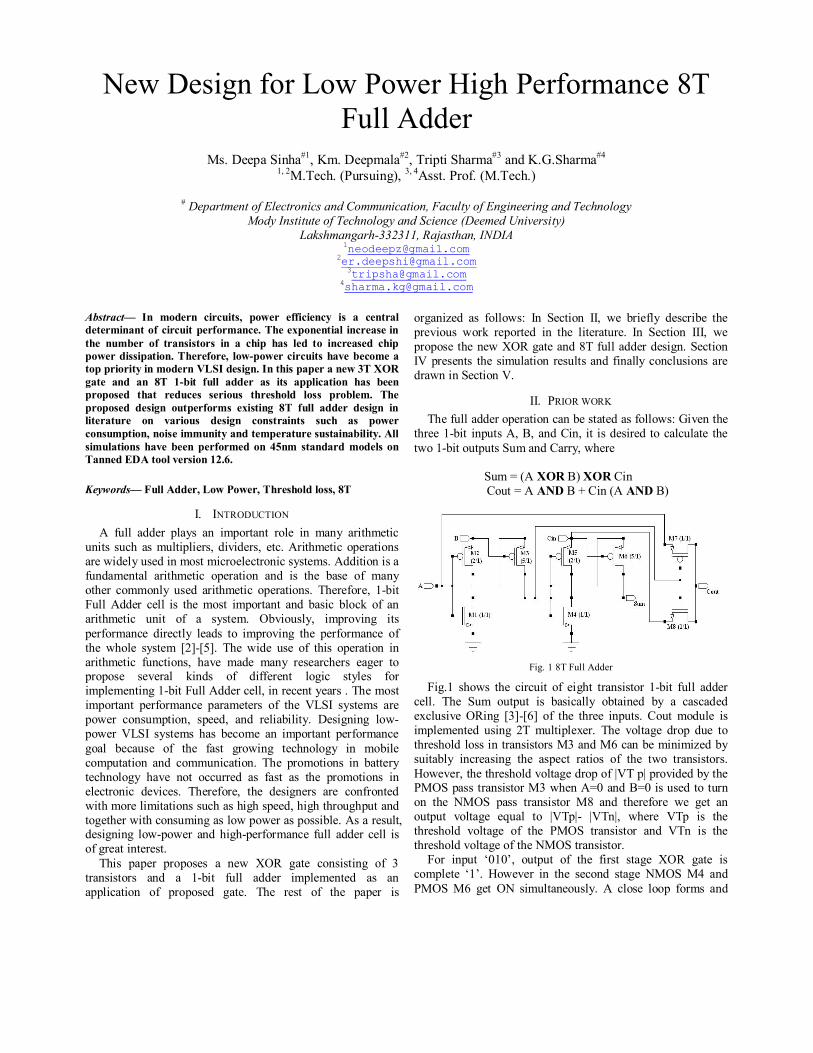
Fig 7: Operating frequency vs Output Noise voltage
Figure 5-7 reveals that the proposed 9T full adder cell proves its superiority in terms of power, power-delay product and noise immunity over existing 8T adder.
5. CONCLUSION This paper proposes a new improved design of 1-bit full adder cell performing efficiently in subthreshold region outperforming the existing 8T full adder. The combination of improved power dissipation, power-delay product, threshold loss and noise immunity makes the proposed full adder a viable option for ultra low power applications.
6. REFERENCE [1] Taur, Y, and Ning, T. H. 1998. Fundamentals of modern
VLSI devices. Cambridge university press, New York. [2] Chandrakasan, A. P et.al. April 1992. Low power CMOS
digital design. in IEEE Jl. Of solid state circuits, vol. 27, pp. 473-484.
[3] Kim, C. H. and Roy, K. 2002. Dynamic VTH scaling schema for active leakage power reducing in Proceedings of Design Automation and Test in European Conference and Exhibition, pp.163 – 167.
[4] Chowdhury, S. R. Banerjee, A. Roy, A. Saha, H. 2008. A high speed 8 transistor full adder design using novel 3 transistor XOR gates in International Journal of Electronics, Circuits and Systems 2, 217
[5] Sharma, T. Sharma, K. G. Singh, B. P. 2010. Energy Efficient 1-bit Full Adder Cell with 45% Reduced Threshold Loss in International Journal of Recent Trends in Engineering, Vol 3, pp. 106-110.
[6] Sharma, T. Sharma, K. G. Singh, B. P. 2010. High Performance Full Adder Cell: A Comparative Analysis. 2010 IEEE Student’s Technology Symposium IIT Kharagpur.
[7] Wang, A. Calhoun, B. H. and Chandrakasan, A. 2005. Sub-threshold design for ultra low-power systems. Springer publishers.
Fig6: Input Voltage vs Power-delay product
New Design for Low Power High Performance 8T Full Adder
Ms. Deepa Sinha#1, Km. Deepmala#2, Tripti Sharma#3 and K.G.Sharma#4
1, 2M.Tech. (Pursuing), 3, 4Asst. Prof. (M.Tech.)
# Department of Electronics and Communication, Faculty of Engineering and Technology Mody Institute of Technology and Science (Deemed University)
Lakshmangarh-332311, Rajasthan, [email protected]
[email protected] [email protected]
Abstract— In modern circuits, power efficiency is a central determinant of circuit performance. The exponential increase in the number of transistors in a chip has led to increased chip power dissipation. Therefore, low-power circuits have become a top priority in modern VLSI design. In this paper a new 3T XOR gate and an 8T 1-bit full adder as its application has been proposed that reduces serious threshold loss problem. The proposed design outperforms existing 8T full adder design in literature on various design constraints such as power consumption, noise immunity and temperature sustainability. All simulations have been performed on 45nm standard models on Tanned EDA tool version 12.6.
Keywords— Full Adder, Low Power, Threshold loss, 8T
I. INTRODUCTION
A full adder plays an important role in many arithmetic units such as multipliers, dividers, etc. Arithmetic operations are widely used in most microelectronic systems. Addition is a fundamental arithmetic operation and is the base of many other commonly used arithmetic operations. Therefore, 1-bit Full Adder cell is the most important and basic block of an arithmetic unit of a system. Obviously, improving itsperformance directly leads to improving the performance of the whole system [2]-[5]. The wide use of this operation in arithmetic functions, have made many researchers eager to propose several kinds of different logic styles for implementing 1-bit Full Adder cell, in recent years . The most important performance parameters of the VLSI systems are power consumption, speed, and reliability. Designing low-power VLSI systems has become an important performance goal because of the fast growing technology in mobile computation and communication. The promotions in battery technology have not occurred as fast as the promotions in electronic devices. Therefore, the designers are confronted with more limitations such as high speed, high throughput and together with consuming as low power as possible. As a result, designing low-power and high-performance full adder cell is of great interest.
This paper proposes a new XOR gate consisting of 3 transistors and a 1-bit full adder implemented as an application of proposed gate. The rest of the paper is
organized as follows: In Section II, we briefly describe the previous work reported in the literature. In Section III, we propose the new XOR gate and 8T full adder design. Section IV presents the simulation results and finally conclusions are drawn in Section V.
II. PRIOR WORK
The full adder operation can be stated as follows: Given the three 1-bit inputs A, B, and Cin, it is desired to calculate the two 1-bit outputs Sum and Carry, where
Sum = (A XOR B) XOR Cin
Cout = A AND B + Cin (A AND B)
Fig. 1 8T Full Adder
Fig.1 shows the circuit of eight transistor 1-bit full adder cell. The Sum output is basically obtained by a cascaded exclusive ORing [3]-[6] of the three inputs. Cout module is implemented using 2T multiplexer. The voltage drop due to threshold loss in transistors M3 and M6 can be minimized by suitably increasing the aspect ratios of the two transistors. However, the threshold voltage drop of |VT p| provided by the PMOS pass transistor M3 when A=0 and B=0 is used to turn on the NMOS pass transistor M8 and therefore we get an output voltage equal to |VTp|- |VTn|, where VTp is the threshold voltage of the PMOS transistor and VTn is the threshold voltage of the NMOS transistor.
For input ‘010’, output of the first stage XOR gate is complete ‘1’. However in the second stage NMOS M4 and PMOS M6 get ON simultaneously. A close loop forms and

current feedback through M4 occurs and the output Sum isdegraded by approx. 50% of the input voltage. Similarly forinput ‘100’, expected Sum should be ‘1’ and Cout to be ‘0’. But the first stage XOR gate gives a degraded output less than input voltage (approx. Input voltage/2). However at higher input voltages (greater than 0.6v) M1 & M3 and M4 & M6 get ON simultaneously. So, there should be minimum loss at first XOR gate, and driving capability of M6 should be high enough than M4. Also for inputs ‘000’ and ‘110’, output of first XOR gate is ‘0’ and when Cin=0, this enables transistors M2 and M3 simultaneously giving a degraded Sum output. Fig.2 shows the input-output waveform of 8T full adder in Fig. 1. As it can be seen, the 8T full adder Figure 1 is confronted with serious problems especially when Cin=0. The outputs have good logic level for only a four input vectors. For the remaining input vectors, there is a major degradation in output voltage that may lead to functional failure as well as increased power consumption. As the voltage is scaled down, the signal integrity deteriorates and the speed decreasestremendously.
III. PROPOSED 8T FULL ADDER
The design of the full adder is based on the design of the XOR gate and a Carry out module. The Carry out module has 6 choices [1] and [2].
A. Proposed 3T XOR Gate
The proposed design of XOR gate is shown in Fig. 2 and its performance result in terms of in-out waveform is shown in Fig.3. It consists of 3 transistors, and input supply voltage(250mv) is given to the gate of NMOS. Due to the supply voltage the NMOS (M3) transistor is always ON. The Out terminal connected to all the Source/Drain of transistor.
When AB=00, both the PMOS transistors are ON and also NMOS is ON due to high gate voltage than threshold. Asmobility of NMOS is nearly three times greater than PMOS, hence it will drive the output ignoring the effect of ON PMOS transistors which results into complete zero output.
When AB=01, M2 is ON and M1 is OFF. As PMOS is strong ‘1’device it will pass complete logic “high” signal atthe output and as NMOS is always on in this design it will be responsible for degradation of voltage at the output. So the voltage at OUT terminal will be slightly less than logic “1”. And Same in when AB =10. When AB=11, both the PMOS transistors are OFF and only NMOS will be responsible fordriving the output to complete zero.
B. Proposed 8T Full Adder
In this paper a new 8T full adder using proposed three transistors XOR gate and a two transistor multiplexer shown in Fig. 4.
Sum = (A XOR B) XOR Cin Cout = A AND B + Cin (A AND B)
Aspect ratio of all the transistors used in proposed full
adder is indicated in Fig. 4. When input AB=00 and 11, the output of first stage of XORing is exact ‘1’, hence is results complete ‘1’ when Cin=0 and a 1.5% of threshold
Fig. 2 Proposed 3T XOR Gate
Fig. 3 In-Out Waveform of 3T XOR Gate
drop when Cin=1. Similarly when AB=01 and 10, there is a threshold drop, however this drop is so less that it can easily be assumed as ‘1’ and gives correct outputs for Cin=0 and 1.
Fig. 5 shows the in-out waveform of existing and proposed 8T full adder and the result reveals that the threshold loss is remarkably reduced in the proposed design which is of great interest in the complex circuit design.
All the substrates terminals in Fig. 1, Fig, 2 and Fig. 4 are connected to their respective source terminals in order to nullify the substrate-bias effect.
IV. SIMULATIONS AND COMPARISONS
All simulations of the proposed 8T full adder and the existing 8T full adder cell have been performed using Tanner EDA Tool version 12.6 on BSIM3v3 45nm technologies with supply voltage ranging from 0.4v to 2v. To establish an impartial simulation circumstance, both the circuits have been tested on the same input patterns which covers every possible combination of A, B and Cin.
In order to test and prove that the proposed design is consuming low power and have high performance; simulations are carried out for power consumption at varying supply voltages. Simulations are also done for proving the superiority of the proposed design over existing one in terms of noise immunity and temperature sustainability and detailed comparison graphs are shown.
Fig.6 and Fig.7 depicts that the proposed full adder cell is outperforming the existing 8T adder in terms of noise immunity and temperature sustainability respectively. Similarly Fig.8 shows that new 8T adder has improved power-delay product than the existing one.
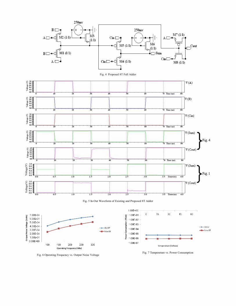
Fig. 4 Proposed 8T Full Adder
Fig. 5 In-Out Waveform of Existing and Proposed 8T Adder
Fig. 6 Operating Frequency vs. Output Noise Voltage
Fig. 7 Temperature vs. Power Consumption

Fig. 8 Input Voltage vs. Power-delay product
V. CONCLUSIONS
The proposed 8T 1-bit full adder is found to give better performance than the existing 8T full adder in various design constraints like power dissipation, power-delay product, noise immunity and threshold drop. The proposed 8T adder has been designed and studied using 45nm technology and can be a viable option for complex circuit design.
REFERENCES [1]. H.T. Bui, Y. Wang and Y. Jiang, “Design and analysis of low-power
10-transistor full adders using XOR-XNOR gates,” IEEE Trans. Circuits Syst. II, Analog Digit. Signal Process, vol. 49, no. 1, pp. 25-30, 2002.
[2]. S. Veeramachaneni, M.B.Srinivas, “New Improved 1-Bit Full Adder Cells,” CCECE/CCGEI, Niagara Falls. Canada, p. 735, May 5-7 2008.
[3]. S.R. Chowdhury, A. Banerjee, A. Roy, H. Saha, “ A high speed 8 transistor full adder design using novel 3 transistor XOR gates,” International Journal of Electronics, Circuits and Systems 2, 217(2008).
[4]. D.Wang, M.Yang, W.Cheng, X.Guan, Z.Zhu, Y.Yang, “Novel Low Power Full Adder Cells in 180nm CMOS Technology,” in Prod. IEEE ICIEA, p. 430, 2009.
[5]. Tripti Sharma, K.G.Sharma, Prof.B.P.Singh, Neha Arora, “A Novel CMOS 1-bit 8T Full Adder Cell,” World Scientific and Engineering Academy and Society (WSEAS) Transactions on Systems, Vol. 9, No.3, pp.317-326, March 2010.
[6]. Tripti Sharma, K.G.Sharma, Prof.B.P.Singh, “Energy Efficient 1-bit Full Adder Cell with 45% Reduced Threshold Loss,” International Journal of Recent Trends in Engineering, Vol 3, pp.106-110, 2010
New Improved 1-Bit 9T Full Adder Cell
Shiwani Singh, Tripti Sharma, K. G. Sharma and Prof. B. P. Singh Department of Electronics & Communication Engineering
Faculty of Engineering & Technology, MITS (Deemed University) Lakshmangarh, INDIA
Email: [email protected], [email protected], [email protected], [email protected]
Abstract— This paper is based on schematic simulations of a proposed design of 9T full adder circuit that shows improved performance than the existing 9T adder. The proposed circuit consists of a new logic which is used to implement Sum module. The proposed design demonstrates the superiority of the proposed adder against existing 9T adder in terms of power–delay product (PDP), temperature sustainability and noise immunity when compared with existing 9T adder while maintaining the constant area. It also shows improvement inthreshold loss as compared to existing 9T full adder for certain input combinations. Therefore, the proposed design outperforms the existing adder in super threshold region and proves to be an optimal option for low power and energy efficient applications. All simulations are performed on 45nm standard model on Tanner EDA tool version 13.0.
Keywords- 9T, XOR gate, full adder, low power and PDP.
I. INTRODUCTION
The increasing prominence of portable systems and need to limit power consumption has led to rapid and innovative developments in low power VLSI design during recent years. The driving forces behind these developments are portable device applications requiring low power consumption and high throughput due to their small chip size with large density of components, increased complexity and high frequencies. As CMOS technologies continue to scale towards the nanometer regime, ultra-low power consumption is the primary requirement while the full swing output is of a secondary importance [1]-[2]. The adder is one of the basic elements in many VLSI systems. It plays an important role in many arithmetic units such as multipliers and dividers. Thus, lowering the power consumption of the adders is an important design objective for low power digital designs. Many design architectures and techniques have been developed to reduce power consumption and has become one of the primary focuses of digital design. There have been many conventional CMOS implementations for full adders. This paper proposes a new 9T circuit which operates efficiently in super threshold region to achieve ultra low power. Results demonstrateimprovement in threshold loss, power consumption, noise immunity and temperature sustainability.
The paper is organized as follows: Section 2 describes an existing 9T full adder as reported in the literature. Section 3 introduces the proposed 9T full adder design. Simulation
results and their comparisons are included in Section 4 andfinally Section 5 concluded the paper.
II. PRIOR WORK
The full adder operation can be stated as follows: Given the three 1-bit inputs A, B, and Cin, it is desired to calculate the two 1-bit outputs Sum and Carry, where
Sum = (A xor B) xor Cin (1) Cout = A and B + Cin (A xor B) (2)
Figure 1. 1-bit 9T Full Adder
The circuit shown in Fig. 1 [3]-[5] is the schematic of modified 8T full adder cell [6]-[7] using an extra transistor M9 to improve the performance of the full adder cell. The Sum output is basically obtained by a cascaded exclusive ORing of the three inputs in addition of an extra transistor M9. Cout is implemented using 2T multiplexer. 8T full adder is confronted with problems when inputs are ABCin=000, 010 and 110 as two transistors get ON simultaneously at the second stage of XOR. Due to reduced device resistance as the ON transistors will have combined parallel effect on resistance results into the degradation of Sum output. This problem is eliminated in the design of Fig.1 by adding an extra transistor M9. Now with inputs 010 and 100, the first stage XOR gate gives ‘1’ which enables the extra added NMOS M9 giving complete ‘0’ and for Cin=0 disable M4. Thus only M6 gets ON to produce the Sum output eliminating the problem of simultaneous enabling of two transistors and hence the output degradation will be removed. This reduces the threshold loss problem and also improves the speed of the circuit. It has area overhead ofone transistor but still its power consumption is reduced than the 8T adder circuit. The transistors M6 of 8T full adder has aspect ratio of (5/1) in order to drive the Sum output to logic high when inputs are 010 while the 9T adder has (1/1) aspect

ratio of transistor M6 in order to drive the Sum output to logic high. Also the extra added transistor M9 has the same aspect ratio of (1/1). The outputs have good logic level only for certain input vectors. For the remaining input vectors, there is a major degradation in output voltage that may lead to functional failure as well as increased power consumption. As the voltage is scaled down, the signal integrity deteriorates and the speed decreases tremendously.
III. PROPOSED 9T FULL ADDER DESIGN
The schematic of proposed 9T full adder cell is shown in Fig. 2 and its truth table is stated in Table I. The operating principle of proposed circuit is different from traditional full adder circuits. The operation of full adder in its conventional form can be stated as follows: Given the three 1-bit inputs A, B and Cin, the Sum and Carry outputs can be calculated as
Sum = (A xor B) xor Cin (3) Cout = A and B + Cin (A xor B) (4)
In proposed design, Cout is implemented by using a 2T
multiplexer which is controlled by output of 3T XOR gate and passes either A or Cin accordingly. An inverter is connected at the output of Cout to generate its complement on which the Sum output is dependent. The operation of Sum module is based on implementing XOR operation between inputs A and B. It is evident from truth table of full adder as stated in Table 1 that when A XOR B is ‘0’, Sum output is equal to input Cin and when A XOR B is ‘1’, Sum output is equal to .. Finally the Sum is obtained by transferring these output levelsthrough 2T multiplexer. This 2T multiplexer is controlled by output of 3T XOR gate.
Figure 2. Proposed 9T Full Adder Cell
This circuit reduces threshold loss problem remarkably and
also improves the overall PDP, output noise voltage and temperature sustainability. The most demanding design constraint for developing compact systems i.e. area, remains constant for both the designs. Fig. 3 shows the in-out waveform of existing 9T and the proposed 9T full adder and the result reveals that the threshold loss is reduced in the proposed design which is of great interest in the complex circuit design. In a nutshell, the proposed 9T full adder has better performance than existing 9T full adder. All the substrate terminals in Fig. 1 and Fig. 2 are connected to their respective source terminals in order to nullify the substrate-bias effect.
IV. SIMULATIONS AND COMPARISON
All schematic simulations are performed on Tanner EDA tool version 13.0 using 45nm technology with input voltage ranges from 1.0V to 2.0 V in steps of 0.2 V. In order to prove that proposed design is consuming low power and has better performance, simulations are carried out for power-delayproduct and output noise voltage at varying temperatures and operating frequencies respectively.
TABLE I. TRUTH TABLE OF PROPOSED 9T FULL ADDER
A B Cin Sum Cout
0 0 0 0 0 Cin 0
0 0 1 0 1 Cin 0
0 1 0 1 1
0
0 1 1 1 0
1
1 0 0 1 1
0
1 0 1 1 0
1
1 1 0 0 0 Cin 1
1 1 1 0 1 Cin 1
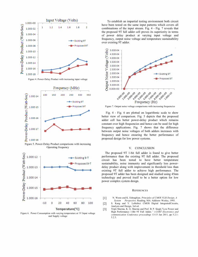
Figure 4. Power-Delay Product with increasing input voltage
Figure 5. Power-Delay Product comparisons with increasing
Operating frequency
Figure 6. Power Consumption with varying temperature at 1V Input voltage
and Supply voltage
To establish an impartial testing environment both circuit
have been tested on the same input patterns which covers all combinations of the input stream. Fig. 4 - Fig. 7 reveals that the proposed 9T full adder cell proves its superiority in terms of power delay product at varying input voltage and frequency, output noise voltage and temperature sustainability over existing 9T adder.
Figure 7. Output noise voltage comparisons with increasing frequencies
Fig. 4 - Fig. 6 are plotted on logarithmic scale to show
better view of comparison. Fig. 5 depicts that the proposed adder cell has better power-delay product which remains constant over high frequencies and hence can be used for high frequency applications. Fig. 7 shows that the difference between output noise voltages of both adders increases with frequency and hence ensuring the better performance of proposed design for low power systems.
V. CONCLUSION
The proposed 9T 1-bit full adder is found to give better performance than the existing 9T full adder. The proposed circuit has been tested to have better temperature sustainability, noise immunity and significantly less power-delay product along with improvement in threshold loss than existing 9T full adder to achieve high performance. The proposed 9T adder has been designed and studied using 45nm technology and proved itself to be a better option for low power complex system design.
REFERENCES
[1] N. Weste and K. Eshraghian, Principles of CMOS VLSI Design, A
System Perspective. Reading, MA: Addison- Wesley, 1993. [2] S. Kang and Y. Leblebici CMOS Digital IntegratedCircuits,
Analysis and Design, 3rd ed. [3] Tripti Sharma, K. G. Sharma and Prof. B. P. Singh,”Low Power and
High Performance 1-Bit 9T Full Adder,” i-COST Electronics and communication Conference proceedings 13-15 Jan 2011, pp 5.2.1-5.2.3.

[4] Deepa Sinha, Tripti Sharma, K. G. Sharma and Prof. B. P. Singh “
Ultra Low Power 1-Bit Full Adder,” International Symposium on Devices MEMS, Intelligent Systems & Communication, International Symposium on Devices MEMS, Intelligent Systems & Communication (ISDMISC) 2011, Proceedings published by International Journal of Computer Applications, pp.09-11.
[5] Deepa Sinha, Tripti Sharma, K. G. Sharma and Prof. B. P. Singh “Energy Efficient Design and Analysis of 1-Bit Full Adder Cell,” in Int. J. on Recent Trends in Engineering & Technology, Vol. 05, No. 02, Mar 2011, pp. 49-52.
Figure 3. In-Out waveforms of Existing 9T Full Adder and Proposed 9T Full Adder Cell
[6] T. Sharma, K.G.Sharma, Prof.B.P.Singh, Neha Arora, “A Novel CMOS 1-bit 8T Full Adder Cell,” in World Scientific and Engineering Academy and Society (WSEAS) Transactions on Systems, vol. 9, No.3, pp. 317-326, March 2010.
[7] S. R. Chowdhury, A. Banerjee, A. Roy, H. Saha, “ A high speed 8transistor full adder design using novel 3 transistor XOR gates,” International Journal of Electronics, Circuits and Systems, vol. 2, No. 4, Fall 2008, pp. 217-223.

Short Paper
Int. J. of Recent Trends in Engineering and Technology, Vol. 4, No. 4, Nov 2010
© 2010 ACEEE
DOI: 01.IJRTET 04.04.75 26
High Speed Array Multipliers Based on
1-Bit Full Adders Tripti Sharma, K.G.Sharma, Prof.B.P.Singh and Neha Arora
FET-MITS (Deemed University)/ Electronics & Communication Deptt., Rajasthan, INDIA
E-mail: [email protected], [email protected], [email protected], [email protected]
Abstract— Array architecture is a popular technique to
implement the multipliers due to its compact structure. In
this paper, three multiplier circuits using 8T, 10TGDIXOR
and 10TGDIXNOR full adders have been designed, simulated,
analyzed and compared. An extensive speed analysis of
multipliers has been done. According to our test results, an
array multiplier designed by 10T GDIXOR full adder is
showing best result in terms of speed with varying supply
voltage. But at the same time the simulation also proves that
the 10T GDIXNOR 1-bit full adder is the fastest among all
other full adders. The simulation has been carried out on
Tanner EDA tool on BSIM3v3 90nm technology.
Index Terms— Full adder, high speed, array multiplier.
I. INTRODUCTION
Multiplication is one of the basic arithmetic operations.
In fact 8.72% of all instructions in a typical scientific
program are multiplies. It is the most important operation
in digital computer systems and digital signal processors.
Besides, multipliers have long latency operations, so
reducing their delay is a key to satisfying the overall speed
of digital VLSI circuits. The basic building block of the
multiplier is the full adder cell, thus it has a significant
effect on the overall performance and speed of the
multiplier. Therefore, high speed full adders based on pass
transistor logic with a low number of transistors were
presented [2]-[6]. Power dissipation and delay in array
multiplier is mainly due to the performance of its
components, namely the Adder and the AND gates as the
basic building blocks of the array structure. Enhancing the
performance of the multiplier can significantly affect the
system performance, therefore, careful design and analysis
is required for these units to obtain optimum performance.
The full adder is the basic building block in array
multipliers and consequently the optimization of its design
is critical for the optimum performance of the multiplier.
The paper is organized as follows. First, Section
II introduces the 8T, 10T GDIXNOR and 10T GDIXOR 1-
bit full adders, then Section III presents the designed array
multipliers, along with their simulation results and then
finally conclusion is written.
II. FULL ADDER: A REVIEW
The full adder operation equations presented below can
be stated as follows: Given the three 1-bit inputs A, B and
Given the three 1-bit inputs A, B and Cin which calculate
_______________________________________________
Corresponding author: Tripti Sharma, email: [email protected]
two 1-bit outputs Sum, for sum and Cout, for carry out.
Figure 1. 8T Full Adder
The transistor level implementation of 8T Full Adder [3]
is shown in Fig.1. The 8T full adder contains three modules
–two cascaded 3T XOR gates to produce Sum output and a
2T multiplexer to produce carry output as shown in
Figure.1. Owing to the appealing traits of a small number
of transistors and a mere 2-transistor delay, it can work at
high speed with low power dissipation.
The transistor level implementation of GDIXOR Full
Adder [2], [3] is shown in Fig.2. This full adder consists of
three modules – two GDI XOR gates and a multiplexer. In
the worst case, sum has 4T delay and Cout has 3T delay.
However, due to the advantages of GDI cell, this circuit
still can achieve its benefit of high speed and low power
consumption.
The transistor level implementation of GDIXNOR Full
Adder [2], [3] is shown in Fig.3. This full adder consists of
three modules – two cascaded GDI XNOR gates and a
multiplexer. Similar to figure.2 it also has a benefit of high
speed and low power consumption.
Graph shown in Fig.4 depicts that the 10T GDIXNOR 1-
bit full adder is the fastest adder among all other adder
cells. But when we implement array multiplier using full
adders then the multiplier using 10T GDIXOR 1-bit full
adder will give the least delay as shown in Section III. This
states that the performance of 10T GDIXNOR full adder is
degraded in terms of speed as we move towards the
complex circuit design.
Short Paper
Int. J. of Recent Trends in Engineering and Technology, Vol. 4, No. 4, Nov 2010
© 2010 ACEEE
DOI: 01.IJRTET 04.04.75 27
Figure 2. 10T GDIXOR Full Adder
Figure 3. 10T GDIXNOR Full Adder
Vdd Vs Delay
0.00E+00
2.00E-09
4.00E-09
6.00E-09
8.00E-09
1.00E-08
1.20E-08
1 1.2 1.4 1.6 1.8 2
Vdd (volts)
De
lay
(se
c)
8T Adder
10T GDIXOR Adder
10T GDIXNOR Adder
Figure 4. Vdd Vs Delay comparison of 1-bit full adders
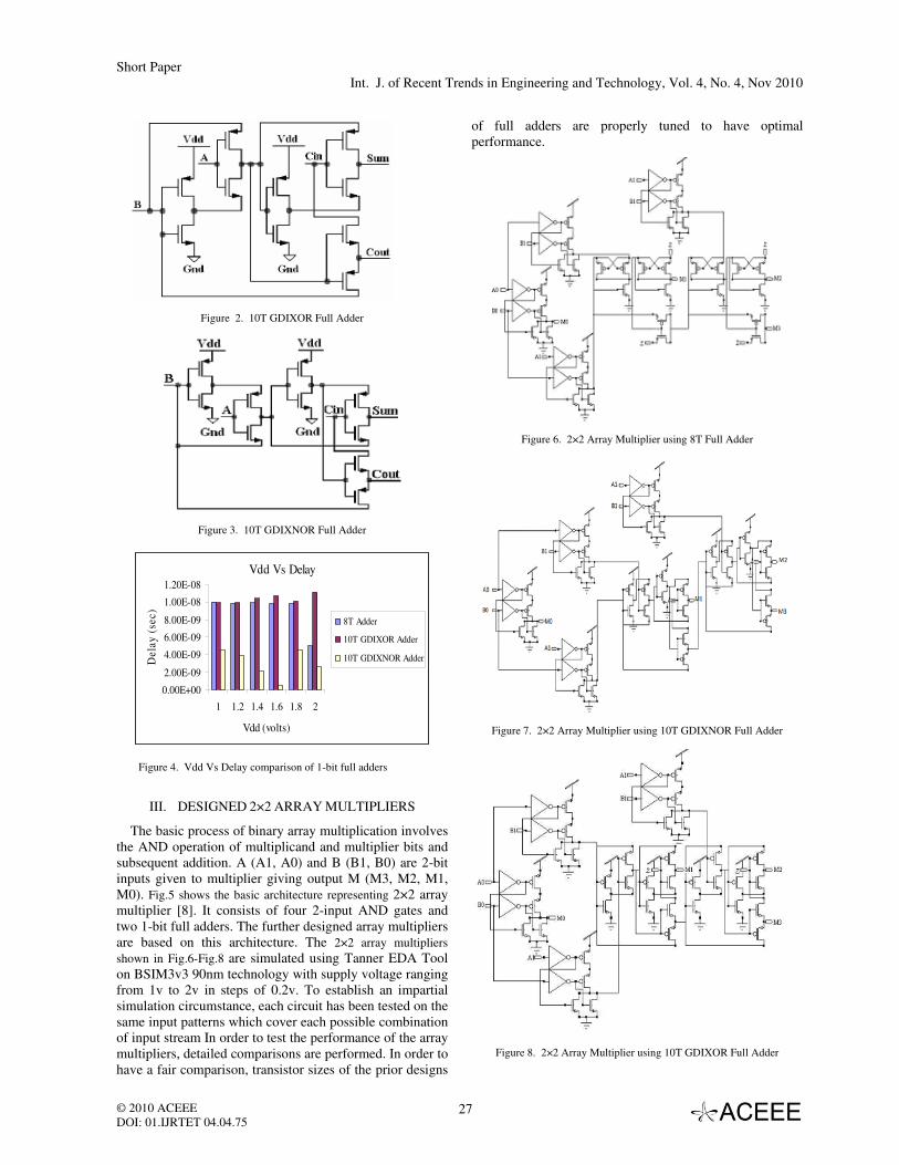
III. DESIGNED 2×2 ARRAY MULTIPLIERS
The basic process of binary array multiplication involves
the AND operation of multiplicand and multiplier bits and
subsequent addition. A (A1, A0) and B (B1, B0) are 2-bit
inputs given to multiplier giving output M (M3, M2, M1,
M0). Fig.5 shows the basic architecture representing 2×2 array
multiplier [8]. It consists of four 2-input AND gates and
two 1-bit full adders. The further designed array multipliers
are based on this architecture. The 2×2 array multipliers
shown in Fig.6-Fig.8 are simulated using Tanner EDA Tool
on BSIM3v3 90nm technology with supply voltage ranging
from 1v to 2v in steps of 0.2v. To establish an impartial
simulation circumstance, each circuit has been tested on the
same input patterns which cover each possible combination
of input stream In order to test the performance of the array
multipliers, detailed comparisons are performed. In order to
have a fair comparison, transistor sizes of the prior designs
of full adders are properly tuned to have optimal
performance.
Figure 6. 2×2 Array Multiplier using 8T Full Adder
Figure 7. 2×2 Array Multiplier using 10T GDIXNOR Full Adder
Figure 8. 2×2 Array Multiplier using 10T GDIXOR Full Adder

Short Paper
Int. J. of Recent Trends in Engineering and Technology, Vol. 4, No. 4, Nov 2010
© 2010 ACEEE
DOI: 01.IJRTET 04.04.75 28
From the graph shown in Fig.9 it is obvious that array
multiplier based on 10T GDIXOR full adder is showing
better results among all other multipliers in the terms of
speed.
Vdd Vs Delay
0.000E+00
1.000E-08
2.000E-08
3.000E-08
4.000E-08
5.000E-08
6.000E-08
1 1.2 1.4 1.6 1.8 2
Vdd (volts)
Del
ay (
sec)
Fig.7
Fig.8
Fig.9
Figure 9. Vdd Vs Delay comparison of 2×2 Array Multipliers
IV. CONCLUSIONS
The paper shows that the 10T GDIXNOR full adder is
the fastest adder among all other adders stated above but at
the same time when these adders are used to design more
complex circuit such as 2×2 array multiplier the 10T
GDIXOR adder proves its superiority over other high speed
adders. Therefore, array multiplier designed by using 10T
GDIXOR full adder is the fastest among all other
multipliers.
REFERENCES
[1] Tripti Sharma, K.G.Sharma, Prof.B.P.Singh, Neha Arora,
“High Speed, Low Power 8T Full Adder Cell with 45%
Improvement in Threshold Loss Problem,” Proceedings of
the 12th
International Conference on Networking, VLSI and
Signal Processing, p. 272, Coimbatore and University of
Cambridge, UK, Feb. 2010.
[2] Tripti Sharma, K.G.Sharma, Prof.B.P.Singh, Neha Arora, “A
Novel CMOS 1-bit 8T Full Adder Cell,” World Scientific
and Engineering Academy and Society (WSEAS)
Transactions on Systems, Vol. 9, No.3, pp.317-326, March
2010.
[3] Prof.B.P.Singh, Tripti Sharma, K.G.Sharma “High Speed and
Energy Efficient Full Adder Cell,” Proceedings of the
National Conference on Innovative Developments in
Electronics Arena, sponsored by IEEE, pp. 102-106, Jaipur,
INDIA, Dec.2009.
[4] S.R. Chowdhury, A. Banerjee, A. Roy, H. Saha, “ A high
speed 8 transistor full adder design using novel 3 transistor
XOR gates,” International Journal of Electronics, Circuits
and Systems 2, 217(2008).
[5] S.Veeramachaneni, M.B.Srinivas, “New Improved 1-Bit Full
Adder Cells,” CCECE/ CCGEI, Niagara Falls. Canada, p.
735, May 5-7 2008.
[6] D.Wang, M.Yang, W.Cheng, X.Guan, Z.Zhu, Y.Yang,
“Novel Low Power Full Adder Cells in 180nm CMOS
Technology,” in Prod. IEEE ICIEA, pp. 430, 2009.
[7] P.M. Lee, C.H. Hsu, Y.H. Hung, “Novel 10-T Full Adder
realized by GDI Structure”, 2007 IEEE international
symposium on integrated circuits (ISIC-2007), pp. 115-118.
[8] Rizwan Mudassir and Z. Abid, “New Parallel Multipliers
Based On Low Power Adders”, CCECE/CCGEI, Saskatoon,
May2005,pp.694-697.
Int. J. on Recent Trends in Engineering & Technology, Vol. 05, No. 02, Mar 2011
© 2011 ACEEEDOI: 01.IJRTET.05.02.113
Short Paper
An Efficient Low Power 3T XOR CellKUMARI DEEPMALA1, TRIPTI SHARMA2, K.G.SHARMA2 and PROF.B.P.SINGH2
1FET-MITS (Deemed University)/ Electronics & Communication Deptt., Rajasthan, INDIAE-mail: [email protected]
2Suresh Gyan Vihar University, Electronics & Communication Deptt., Jaipur, Rajasthan, INDIAE-mail: [email protected], [email protected], [email protected]
Abstract—This paper presents a XOR cell that can beimplemented in CMOS technology. The design has beencompared with existing 3T XOR cell and found a significantimprovement in power consumption, power-delay product,noise immunity and parasitic capacitances. The pre layoutsimulation has been carried out on Tanner EDA tool onBSIM3v3 45nm technology and post layout simulation on0.5submicron technology.
Index Terms—XOR gate, low power, noise immunity and power-delay product.
I. INTRODUCTION
The exclusive-OR (XOR) function is the fundamental unitin various circuits, such as comparator, parity checker, fulladder, multiplier and so on. The design of XOR has beenundergoing a considerable improvement, being motivated bythe basic design goals, viz. minimizing the transistor count,minimizing the power consumption and high throughput.Enhancing the performance of the XOR gates cansignificantly improve the performance of any gate level logic[1].Using lower number of transistors to implement a logicfunction is beneficial in reducing the number of componentsand interconnect parasitic and reducing the chip area,resulting in lower time delay and potentially lower powerconsumption. However, many low-number-transistors XORdo not operate correctly at low supply voltage in 0.09ì andsubsequent CMOS technologies due to threshold lossproblem [2]. Therefore, the prime goal now-a-days is to designthe low-number-of-transistors that works successfully at lowsupply voltage, reduces degradation on the output voltageand consumes less power. The rest of the paper is organizedas follows: In Section II, we briefly describe the previouswork reported in the literature. The proposed 3T XOR gatedesign and its working is explained in Section III. Simulationanalysis and results are stated in Section IV and finallyconclusion is drawn in Section V.
II. PREVIOUS WORK
The design shown in Fig.1 [2]-[4], [6] and [7] is based ona modified version of a CMOS inverter and a PMOS passtransistor. When the input B is at logic high, the inverterfunctions like a normal CMOS inverter. When the input B is
Corresponding address: Tripti Sharma, K.G.Sharma and Prof.B.P.SinghFET-MITS (Deemed University), Lakshmangarh-332311,RAJASTHANEmail: tr [email protected], [email protected] [email protected]
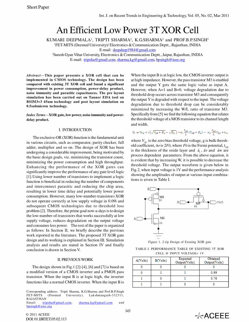
When the input B is at logic low, the CMOS inverter output isat high impedance. However, the pass transistor M3 is enabledand the output Y gets the same logic value as input A.However, when A=1 and B=0, voltage degradation due tothreshold drop occurs across transistor M3 and consequentlythe output Y is degraded with respect to the input. The voltagedegradation due to threshold drop can be considerablyminimized by increasing the W/L ratio of transistor M3.Specifically from [5] we find the following equation that relatesthe threshold voltage of a MOS transistor to its channel lengthand width.
where VT0 is the zero bias threshold voltage, g is bulk thresh-old coefficient, öo is 2Fö, where Fö is the Fermi potential, tOXis the thickness of the oxide layer and ál , áv and áw areprocess dependent parameters. From the above equation, itis evident that by increasing W, it is possible to decrease thethreshold voltage. The output waveform is given below inFig.2, when input voltage is 1V and the performance analysisshowing the amplitudes of output at various input combina-tions is given in Table I.
Figure 1. 2-i/p Design of Existing XOR gate
TABLE I. PERFORMANCE TABLE OF EXISTING 3T XORCELL @ INPUT VOLTAGE= 1V
143

Int. J. on Recent Trends in Engineering & Technology, Vol. 05, No. 02, Mar 2011
© 2011 ACEEEDOI: 01.IJRTET.05.02.113
Short Paper
Figure 2. In-Out Waveform of Existing XOR gate
III. PROPOSED 3T XOR GATE
The design of proposed XOR gate is shown below inFig.3. The proposed XOR cell consists of 3 transistors, andinput supply voltage (250mv) is given to the gate of NMOS.Due to the supply voltage the NMOS (M3) transistor is alwaysON. The Out terminal connected to all the Source/Drain oftransistor.
Figure 3. 2-i/p Design of Proposed XOR gate
When AB=00, both the PMOS transistors are ON and alsoNMOS is ON due to high gate voltage than threshold. Asmobility of NMOS is nearly three times greater than PMOS,hence it will drive the output ignoring the effect of ON PMOStransistors which results into complete zero output.
TABLE II. PERFORMANCE TABLE OF PROPOSED 3T XORCELL @ INPUT VOLTAGE = 1V
When AB=01, M2 is ON and M1 is OFF. As PMOS is strong‘1’device it will pass complete logic “high” signal at the out-put but as NMOS is always ON, so due to parallel resistanceof both the devices the output will be slightly degraded thanlogic “1” and similar case will happen with AB =10.
Now for AB=11, both the PMOS transistors are OFF andonly NMOS will be responsible for driving the output tocomplete zero. The performance table shown in Table II makesit obvious that the output is degraded by only 1.015% thanlogic HIGH. Fig. 4 shows the input-output waveform wheninput voltage is at 1v.
Figure 4. In-Out Waveform of Proposed XOR gate
IV. SIMULATION AND PERFORMANCE ANALYSIS
In order to test the performance of proposed XOR cell,detailed comparisons are performed. The existing andproposed designs are simulated using BSIM 3v3 45nmtechnology on Tanner EDA tool. To establish an impartialtesting environment, both the circuits are simulated on sameinput patterns. And the post-layout simulations of XOR gatedesign are carried out on 0.5 submicron technology to extractthe parasitic capacitance produced. Simulation results shownin Fig.5-Fig.7 depicts that the proposed XOR cell is the viableoption for efficient design.
Figure 5. Input Voltage vs. Power Consumption
144
Int. J. on Recent Trends in Engineering & Technology, Vol. 05, No. 02, Mar 2011
© 2011 ACEEEDOI: 01.IJRTET.05.02.113
Short Paper
Figure 6. Input Voltage vs. PDP
Figure 7. Operating Frequency vs. Output Noise Voltage
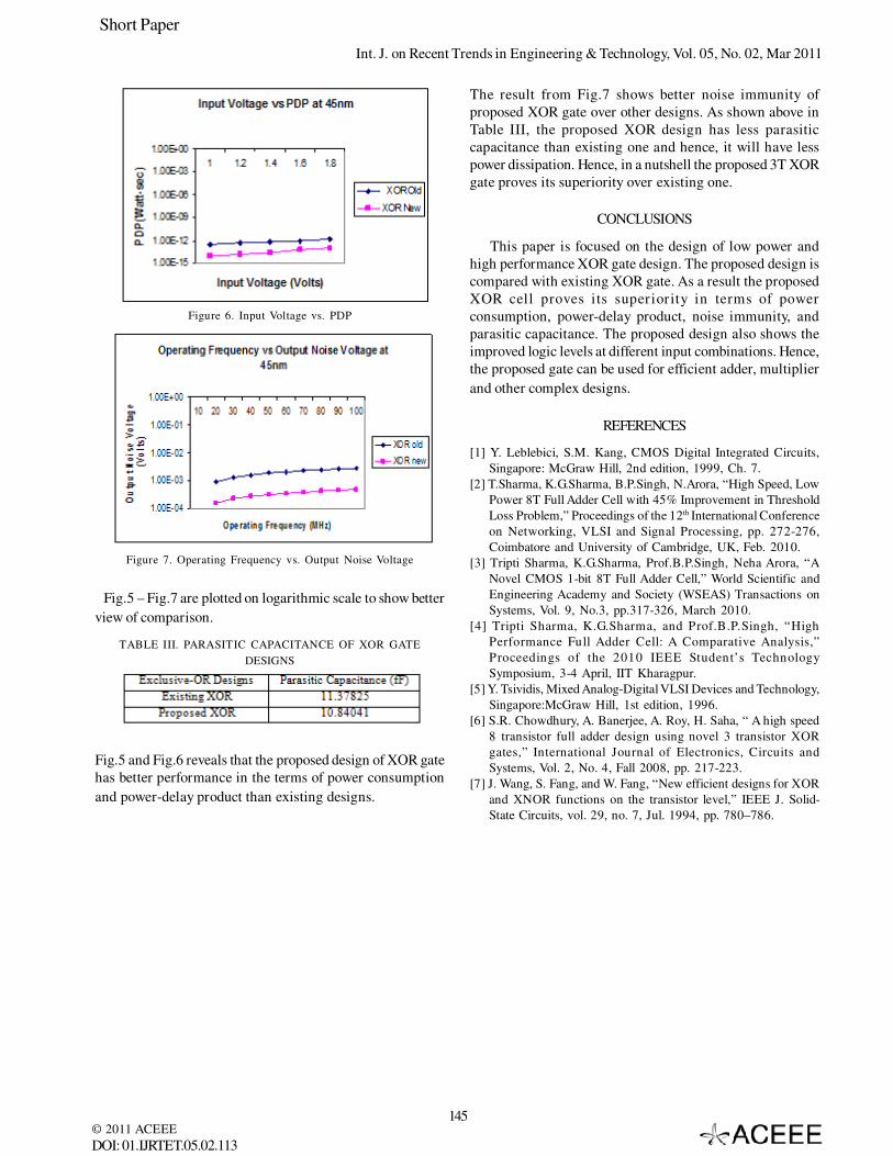
Fig.5 – Fig.7 are plotted on logarithmic scale to show betterview of comparison.
TABLE III. PARASITIC CAPACITANCE OF XOR GATEDESIGNS
Fig.5 and Fig.6 reveals that the proposed design of XOR gatehas better performance in the terms of power consumptionand power-delay product than existing designs.
The result from Fig.7 shows better noise immunity ofproposed XOR gate over other designs. As shown above inTable III, the proposed XOR design has less parasiticcapacitance than existing one and hence, it will have lesspower dissipation. Hence, in a nutshell the proposed 3T XORgate proves its superiority over existing one.
CONCLUSIONS
This paper is focused on the design of low power andhigh performance XOR gate design. The proposed design iscompared with existing XOR gate. As a result the proposedXOR cell proves its superiority in terms of powerconsumption, power-delay product, noise immunity, andparasitic capacitance. The proposed design also shows theimproved logic levels at different input combinations. Hence,the proposed gate can be used for efficient adder, multiplierand other complex designs.
REFERENCES
[1] Y. Leblebici, S.M. Kang, CMOS Digital Integrated Circuits,Singapore: McGraw Hill, 2nd edition, 1999, Ch. 7.
[2] T.Sharma, K.G.Sharma, B.P.Singh, N.Arora, “High Speed, LowPower 8T Full Adder Cell with 45% Improvement in ThresholdLoss Problem,” Proceedings of the 12th International Conferenceon Networking, VLSI and Signal Processing, pp. 272-276,Coimbatore and University of Cambridge, UK, Feb. 2010.
[3] Tripti Sharma, K.G.Sharma, Prof.B.P.Singh, Neha Arora, “ANovel CMOS 1-bit 8T Full Adder Cell,” World Scientific andEngineering Academy and Society (WSEAS) Transactions onSystems, Vol. 9, No.3, pp.317-326, March 2010.
[4] Tripti Sharma, K.G.Sharma, and Prof.B.P.Singh, “HighPerformance Full Adder Cell: A Comparative Analysis,”Proceedings of the 2010 IEEE Student’s TechnologySymposium, 3-4 April, IIT Kharagpur.
[5] Y. Tsividis, Mixed Analog-Digital VLSI Devices and Technology,Singapore:McGraw Hill, 1st edition, 1996.
[6] S.R. Chowdhury, A. Banerjee, A. Roy, H. Saha, “ A high speed8 transistor full adder design using novel 3 transistor XORgates,” International Journal of Electronics, Circuits andSystems, Vol. 2, No. 4, Fall 2008, pp. 217-223.
[7] J. Wang, S. Fang, and W. Fang, “New efficient designs for XORand XNOR functions on the transistor level,” IEEE J. Solid-State Circuits, vol. 29, no. 7, Jul. 1994, pp. 780–786.
145

Review Paper
© 2011 ACEEEDOI: 01.IJRTET.06.01.
Int. J. on Recent Trends in Engineering and Technology, Vol. 6, No. 1, Nov 2011
222
New 9T Full Adder Design with 30% ReducedThreshold Loss
Tripti Sharma1, Shiwani Singh2, K. G. Sharma1 and Prof. B. P. Singh1
1Suresh Gyan Vihar University, Department of ECE, Jaipur, INDIAEmail: [email protected], [email protected], [email protected]
2FET-MITS, Department of ECE, Lakshmangarh, INDIAEmail: [email protected]
Abstract- This paper is based on pre layout simulations of 8Tand new proposed 9T full adder circuit that improves theperformance of 8T adder by sacrificing the MOS transistorcount by one. The proposed circuit consists of a new logicwhich is used to implement Sum module. The proposed designremarkably reduces power consumption hence power-delayproduct (PDP) and improves temperature sustainability whencompared with an existing 8T adder. It also shows nearly 30%improvement in threshold loss as compared to 8T full adder.Therefore, in a nut shell proposed adder cell outperforms theexisting 8T adder in super threshold region and proves to be aviable option for low power and energy efficient applications.All simulations are performed on 90nm standard model onTanner EDA tool version 12.6.
Index Terms- Full Adder, 8T, 9T, XOR, PDP and low power.
I. INTRODUCTION
Advances in CMOS technology have led to a renewedinterest in the design of basic functional units for digitalsystems. The design of high-speed and low-power VLSIarchitectures needs efficient arithmetic processing units,which are optimized for the performance parameters, namely,speed and power consumption [1] and [2]. Addition is one ofthe fundamental arithmetic operations. It is used extensivelyin many VLSI systems such DSP architectures,microprocessors, etc. In addition to its main task which isadding two binary numbers, it is the nucleus of many otheruseful operations such as subtraction, multiplication, division,etc. So, it is very important to choose the adder topologythat would yield the desired performance. That’s why, buildinglow-power, high performance adder cells are of great interestand any modifications made to the full adder would affect thesystem as a whole.To meet the growing demand, this paper proposes a new 9Tfull adder circuit which operates efficiently in super thresholdregion to achieve low power and hence PDP. Resultsdemonstrate improvement in threshold loss, powerconsumption and temperature sustainability. The rest of thepaper is organized as follows: Section II describes theoperation of existing 8T full adder as reported in the literature.Section III describes the proposed 9T full adder design indetail. Pre layout simulation results are discussed in SectionIV and finally Section V ends the paper with conclusion.Address of Correspondence: T.Sharma, FET-MITS, Department ofECE, Lakshmangarh, INDIA. E-mail: [email protected]
II. PRIOR WORK
The full adder operation can be stated as follows: Giventhe three 1-bit inputs A, B, and Cin, it is desired to calculatethe two 1-bit outputs Sum and Carry, where
Sum = (A xor B) xor Cin (1) Cout = A and B + Cin (A xor B) (2)
Figure 1. 1-bit 8T Full Adder
Fig. 1 shows the circuit of eight transistor 1-bit full addercell. The Sum output is basically obtained by a cascadedexclusive ORing [3]-[7] of the three inputs. Cout isimplemented using 2T multiplexer. It is quite evident fromFig.1 that two stage delays are required to obtain the Sumoutput and at most two stage delays are required to obtainthe carry output Cout. The voltage drop due to thresholdloss in transistors M3 and M6 in Fig.1 can be minimized bysuitably increasing the aspect ratio of the two transistors.However, the threshold voltage drop of |VTp| provided by thePMOS pass transistor M3 when A=0 B=0 is used to turn onthe NMOS pass transistor M8 and therefore we get an outputvoltage equal to |VTp| - VTn, where |VTp| I the threshold voltageof the NMOS transistor.
For input ‘010’, output of the first stage XOR gate iscomplete ‘1’. However in the second stage NMOS M4 andPMOS M6 get ON simultaneously. A close loop forms andcurrent feedback through M4 occurs and the output Sum isdegraded by approx. 50% of the input voltage. Similarly forinput ‘100’, expected Sum should be ‘1’ and Cout to be ‘0’.But the first stage XOR gate gives a degraded output lessthan input voltage (approx. Input voltage/2). However athigher input voltages (greater than 0.6v) M1 & M3 and M4 &M6 get ON simultaneously. So, there should be minimumloss at first XOR gate, and driving capability of M6 should

Review Paper
© 2011 ACEEEDOI: 01.IJRTET.06.01.
Int. J. on Recent Trends in Engineering and Technology, Vol. 6, No. 1, Nov 2011
222
be high enough than M4. Also for inputs ‘000’ and ‘110’,output of first XOR gate is ‘0’ and when Cin=0, this enablestransistors M2 and M3 simultaneously giving a degradedSum output.
As it can be seen, the 8T full adder Fig.1 is confrontedwith serious problems especially when Cin=0. The outputshave good logic level for only a four input vectors. For theremaining input vectors, there is a major degradation in outputvoltage that may lead to functional failure as well as increasedpower consumption. As the voltage is scaled down, the signalintegrity deteriorates and the speed decreases tremendously.
III. PROPOSED 9T FULL ADDER DESIGN
The schematic of proposed 9T full adder cell is shown inFig. 2 and its truth table is stated in Table I. The operatingprinciple of proposed circuit is different from traditionalcircuits. The operation of full adder in its traditional form canbe stated as follows: Given the three 1 bit inputs A, B andCin, the Sum and Carry outputs can be calculated as Sum = (A xor B) xor Cin (3) Cout = A and B + Cin (A xor B) (4)
For generating the Sum output in the proposed design,the truth table has been divided into two parts, one for inputA= ‘0’ and another for A= ‘1’ rather than implementing theconventional Sum module. From the truth table shown inTable I it is evident that when A= ‘0’, Sum can be producedby XORing inputs B and Cin. Similarly, when A= ‘1’, Sum isshowing the XNORing between inputs B and Cin. Therefore,the operation of Sum module is based on implementing XORoperation and XNOR operation between inputs B and Cin.
An inverter is connected at the output of first stage XORgate to generate XNOR function. Finally the Sum isimplemented by transferring these output levels through 2Tmultiplexer. Input to PMOS transistor M6 is XOR of B andCin while to NMOS M7, input is XNOR ofB and Cin. This 2Tmultiplexer is controlled by input A.
Cout is implemented by using another 2T multiplexerwhich is controlled by output of first stage XOR gate andpasses either A or Cin accordingly. This circuit reducesthreshold loss problem by 30% and also improves the overallPDP and temperature sustainability of the circuit.
Figure 2. Proposed 9T Full Adder Cell
TABLE I. TRUTH TABLE OF FULL ADDER
Fig. 3 shows the in-out waveform of existing 8T andproposed 9T full adder and the result reveals that the thresholdloss is remarkably reduced in the proposed design which isof great interest in the complex circuit design. It has areaoverhead of one transistor but still its power consumption isremarkably reduced than the 8T full adder circuit. The 8Tadder circuit in Fig.1 has 5/1 aspect ratio of transistor M6 inorder to drive Sum output to logic high but the adder shownin Fig. 5 has 1/1 aspect ratio of transistor M6 to drive Sumoutput to logic high and extra added transistor M9 has thesame 1/1 aspect ratio.
Therefore, the proposed design will not affect the area bylarge extent. In a nutshell, the proposed 9T full adder hasbetter performance than existing 8T full adder. All thesubstrates terminals in Fig. 1 and Fig. 2 are connected to theirrespective source terminals in order to nullify the substrate-bias effect.
IV. SIMULATIONS AND COMPARISON
All schematic simulations are performed on Tanner EDAtool version 12.6 using 90nm technology with input voltageranges from 1.0V to 2.0 V in steps of 0.2 V. In order to provethat proposed design is consuming low power and have highperformance, simulations are carried out for power, power-delay product at varying supply voltages and temperatures.
To establish an impartial testing environment both circuithave been tested on the same input patterns which covers allcombinations of the input stream. Fig. 4 - Fig. 6 reveals thatthe proposed 9T full adder cell proves its superiority in termsof power consumption, power delay product and temperaturesustainability over existing 8T adder. Fig. 4 and Fig. 5 areplotted on logarithmic scale to show better view ofcomparison.
Figure 4. Power consumption with increasing input voltage

Review Paper
© 2011 ACEEEDOI: 01.IJRTET.06.01.
Int. J. on Recent Trends in Engineering and Technology, Vol. 6, No. 1, Nov 2011
222
Figure 3. In-Out waveforms of Existing 8T Full Adder and Proposed 9T Full Adder Cell
Figure 5. Power-Delay Product comparisons with increasing inputvoltage
Figure 6. Power Consumption with varying temperature at 1V Inputvoltage and Supply voltage
CONCLUSION
The proposed 9T 1-bit full adder is found to give betterperformance than the existing 8T full adder at the cost ofnegligible area overhead. The proposed circuit has beentested to have better temperature sustainability andsignificantly less power delay product along with 30%improvement in threshold loss than 8T full adder to achievehigh performance. The proposed 8T adder has been designedand studied using 90nm technologyand can be a viable optionfor low power complex circuit design.
REFERENCES
[1] N. Weste and K. Eshraghian, Principles of CMOS VLSI Design,A System Perspective. Reading, MA: Addison-Wesley, 1993.[2] S. Kang and Y. Leblebici, CMOS Digital Integrated Circuits,Analysis and Design, 3rd ed.[3] S.Veeramachaneni, M.B.Srinivas, “New Improved 1-Bit FullAdder Cells,” CCECE/ CCGEI, Niagara Falls. Canada, pp. 735-738, May 5-7 2008.[4] T. Sharma, K.G.Sharma, Prof.B.P.Singh, Neha Arora, “A NovelCMOS 1-bit 8T Full Adder Cell,” in World Scientific and EngineeringAcademy and Society (WSEAS) Transactions on Systems, vol. 9,No.3, pp. 317-326, March 2010.[5] D.Wang, M.Yang, W.Cheng, X.Guan, Z.Zhu, Y.Yang, “NovelLow Power Full Adder Cells in 180nm CMOS Technology,” inProd.IEEE ICIEA, pp. 430-433, 2009.[6] S. R. Chowdhury, A. Banerjee, A. Roy, H. Saha, “ A high speed8-transistor full adder design using novel 3 transistor XOR gates,”International Journal of Electronics, Circuits and Systems, vol. 2,No. 4, pp. 217-223, 2008.[7] T. Sharma, K. G. Sharma and Prof. B. P. Singh, “Energy Efficient1-bit Full Adder Cell with 45% Reduced Threshold Loss,”International Journal of Recent Trends in Engineering, vol 3, pp.106-110, 2010.

Hindawi Publishing CorporationVLSI DesignVolume 2012, Article ID 248347, 5 pagesdoi:10.1155/2012/248347
Research Article
9T Full Adder Design in Subthreshold Region
Shiwani Singh,1 Tripti Sharma,2 K. G. Sharma,2 and B. P. Singh1
1 Faculty of Engineering & Technology, MITS (Deemed University), Lakshmangarh 332311, India2 Department of Electronics & Communication, Suresh Gyan Vihar University, Jaipur, India
Correspondence should be addressed to Tripti Sharma, [email protected]
Received 22 October 2011; Revised 21 December 2011; Accepted 26 December 2011
Academic Editor: Jose Silva-Martinez
Copyright © 2012 Shiwani Singh et al. This is an open access article distributed under the Creative Commons Attribution License,which permits unrestricted use, distribution, and reproduction in any medium, provided the original work is properly cited.
This paper presents prelayout simulations of two existing 9T and new proposed 9T full adder circuit in subthreshold region toemploy in ultralow-power applications. The proposed circuit consists of a new logic which is used to implement Sum module. Theproposed design remarkably reduces power-delay product (PDP) and improves temperature sustainability when compared withexisting 9T adders. Therefore, in a nut shell proposed adder cell outperforms the existing adders in subthreshold region and provesto be a viable option for ultralow-power and energy-efficient applications. All simulations are performed on 45 nm standard modelon Tanner EDA tool version 13.0.
1. Introduction
Advances in CMOS technology have led to a renewed interestin the design of basic functional units for digital systems.The use of integrated circuits in high-performance com-puting, telecommunications, and consumer electronics hasbeen growing at a very fast pace. This trend is expectedto continue, with very important implications for power-efficient VLSI and systems designs.
Digital integrated circuits commonly use CMOS circuitsas building blocks. The continuing decrease in feature size ofCMOS circuits and corresponding increase in chip densityand operating frequency have made power consumption amajor concern in VLSI design. Excessive power dissipation inintegrated circuits not only discourages their use in portableenvironment but also causes overheating which reduces chiplife and degrades performance.
Computations in these devices need to be performedusing low-power, area efficient circuits operating at greaterspeed. The design of high-speed and low-power VLSI archi-tectures needs efficient arithmetic processing units, which areoptimized for the performance parameters, namely, speedand power consumption [1, 2].
Addition is one of the widely used fundamental arith-metic operations. In addition to its main task, which isadding two binary numbers, it is the nucleus of many otheruseful operations such as subtraction, multiplication, and
division. Full adder is an essential component for designingall types of processors, namely, digital signal processors(DSP), microprocessors, and so forth.
In most of the digital systems adder lies in the criticalpath that affects the overall speed of the system.
It is very important to choose the adder topology thatwould yield the desired performance. So enhancing theperformance of the 1-bit full adder cell is the main designaspect.
One way to achieve ultralow is by running digital circuitsin subthreshold mode [1, 2]. Subthreshold current of anMOSFET transistor occurs when the gate-to-source voltage(VGS) of a transistor is lower than its threshold voltage(VTH). When VGS is larger than VTH, majority carriers arerepelled from the gate area of the transistor and a minoritycarrier channel is created. This is known as strong-inversion,as more minority carriers are present in the channel thanmajority carriers. When VGS is lower than VTH, there areless minority carriers in the channel, but their presencecomprises a current and the state is known as weak-inversion.In standard CMOS design, this current is a subthresholdparasitic leakage, but if the supply voltage (VDD) is loweredbelow VTH, the circuit can be operated using the subthresh-old current with ultralow-power consumption.
The proposed circuit operates efficiently in subthresholdregion to achieve ultralow power. Results show improvementin temperature sustainability and PDP over the other adders

2 VLSI Design
with comparable performance. The rest of the paper isorganized as follows. Section 2 briefly describes the previouswork reported in the literature. Proposed 9T Adder cell isdescribed in Section 3. Section 4, presents the simulationresults and conclusions are drawn in Section 5.
2. Prior Work
The full adder operation can be stated as follows. Given thethree 1-bit inputs A, B, and Cin, it is desired to calculate thetwo 1-bit outputs Sum and Cout, where
Sum = A⊕ B ⊕ Cin, (1)
Cout = A · B + Cin(A⊕ B). (2)
The circuit shown in Figure 1 [3–5] is the schematic ofmodified 8T full adder cell [6–9] using an extra transistorM9 to improve the performance of the 8T full adder cell.The Sum output is basically obtained by a cascaded exclusiveORing of the three inputs in addition to an extra transistorM9. Cout is implemented using 2T multiplexer. 8T full adderis confronted with problems for certain input vectors. Thisproblem is eliminated in the design of Figure 1 by adding anextra transistor M9. Although it has area overhead of onetransistor, but still its power consumption is reduced thanthe 8T adder circuit. The outputs have good logic level onlyfor certain input vectors. For the remaining input vectors,there is a major degradation in output voltage that may leadto functional failure as well as increased power consumptionat higher voltages. An extra added transistor M9 remainsON for 010 and 100 input combinations also but does notcontribute to produce Sum output and hence results intoexcess power consumption.
Figure 2 shows schematic of another 9T full adder design[10] reported in literature. In this circuit, a three-transistorXOR gate [6–9] and a multiplexer are used to implementSum and one multiplexer to implement the Cout. Theselector circuit of the output multiplexers is output of first-stage XOR. This circuit shows nominal improvements inpower when compared with adder of Figure 1 in subthresh-old region. The reason for less power consumption than thecircuit of Figure 1 is shown in Table 2.
3. Proposed 9T Full Adder Design
The schematic of proposed 9T full adder cell is shown inFigure 3 and its truth table is stated in Table 1. The operatingprinciple of proposed circuit is different from traditionalcircuits. For generating the Sum output in the proposeddesign, the truth table has been divided into two parts, onefor input A = “0” and another for A = “1” rather thanimplementing the conventional Sum module of (1). Fromthe truth table shown in Table 1 it is evident that whenA = “0”, Sum can be produced by XORing inputs B andCin. Similarly, when A = “1”, Sum is showing the XNORingbetween inputs B and Cin. Therefore, the operation ofSum module is based on implementing XOR operationand XNOR operation between inputs B and Cin which is
Table 1: Truth table of 1-bit full adder.
A B Cin Sum Cout
0 0 0 0 0
0 0 1 1 0
0 1 0 1 0
0 1 1 0 1
1 0 0 1 0
1 0 1 0 1
1 1 0 0 1
1 1 1 1 1
indicated in (3) and (4). The logic for Cout output is statedin (5) and (6).
When A = 0,
Sum = B ⊕ Cin. (3)
When A = 1,
Sum = B � Cin. (4)
For Cout, when B ⊕ Cin = 0,
Cout = Cin. (5)
When B � Cin = 1,
Cout = A. (6)
An inverter is connected at the output of first-stage XOR gateto generate XNOR function. Finally the Sum is implementedby transferring these output levels through 2T multiplexer.Input to the PMOS (M6) of 2T multiplexer is XOR of B andCin while to NMOS (M7) is XNOR of B and Cin. This 2Tmultiplexer is controlled by input A. Cout is implemented byusing another 2T multiplexer which is controlled by outputof first-stage XOR gate and passes either A or Cin accordingly.This circuit reduces the overall PDP at varying input voltagesand operating frequencies and also improves the temperaturesustainability while operating in subthreshold region. Themost demanding design constraint for developing compactsystems, that is, area, remains constant for all three designs.
Total power consumption in MOS logic circuits is ex-pressed as sum of three components [2] as shown in (7):
PTotal = PSwitching + PSub + PShort circuit, (7)
where Pswitching denotes the average switching power con-sumption and is given by (8)
PSwitching = αTCloadV2DD f . (8)
Since no external load capacitance is connected in the circuit,hence total capacitance is only due to parasitic present in thedesign. Therefore at constant frequency and supply voltage,αT (switching activity factor) will be the dominant factorwhich determines the total switching power of the circuit.
PSub denotes subthreshold power consumption and isgiven by (9)
PSub = VDD × ISub, (9)

VLSI Design 3
Sum
Cout
Cin
A
B
M2 (2/1) M3 (5/1)
M1 (1/1)
M5 (2/1)
M9 (1/1)
M4 (1/1)
M6 (1/1)M7 (1/1)
M8 (1/1)
N2 N3
N1
Cin
Figure 1: Existing 1-bit 9T full adder.
Sum
Cout
AB
B
C
C
M2 (2/1) M3 (5/1)
M1 (1/1)
M5 (1/1)
M4 (1/1)
M6 (1/1)
M9 (1/1)
M7 (1/1)
M8 (1/1)
N1
N3
N2
Figure 2: Existing 1-bit 9T full adder.
Sum
CoutB A
M2 (2/1)
M1 (1/1)
M3 (5/1)
M5 (1/1)
M4 (1/1)
M6 (1/1)
M7 (1/1)
M8 (1/1)
M9 (1/1)
N1 N2
N3
Cin
Figure 3: Proposed 9T full adder cell.
4 VLSI Design
Table 2: No. of power consuming transitions at different internalnodes.
Figure 1 Figure 2 Proposed 9T(Figure 3)
N1 N2 N3 N1 N2 N3 N1 N2 N3
1 4 3 1 3 3 2 2 3
Total = 8 Total = 7 Total = 7
where
ISub = K × exp
�(VGS −Vt)q
ηKT
�,
�
1− exp�VDS
q
KT
��.
(10)
As shown in (10), the reduced value of VGS in subthresholdmode decreases current exponentially and thus reducessubthreshold power.
PShort circuit is due to the large rise and fall times ofinput voltage. But in all the designs included in this paperthe default rise and fall time of 1 nsec has been taken forsimulation which results into negligible short circuit powerconsumption.
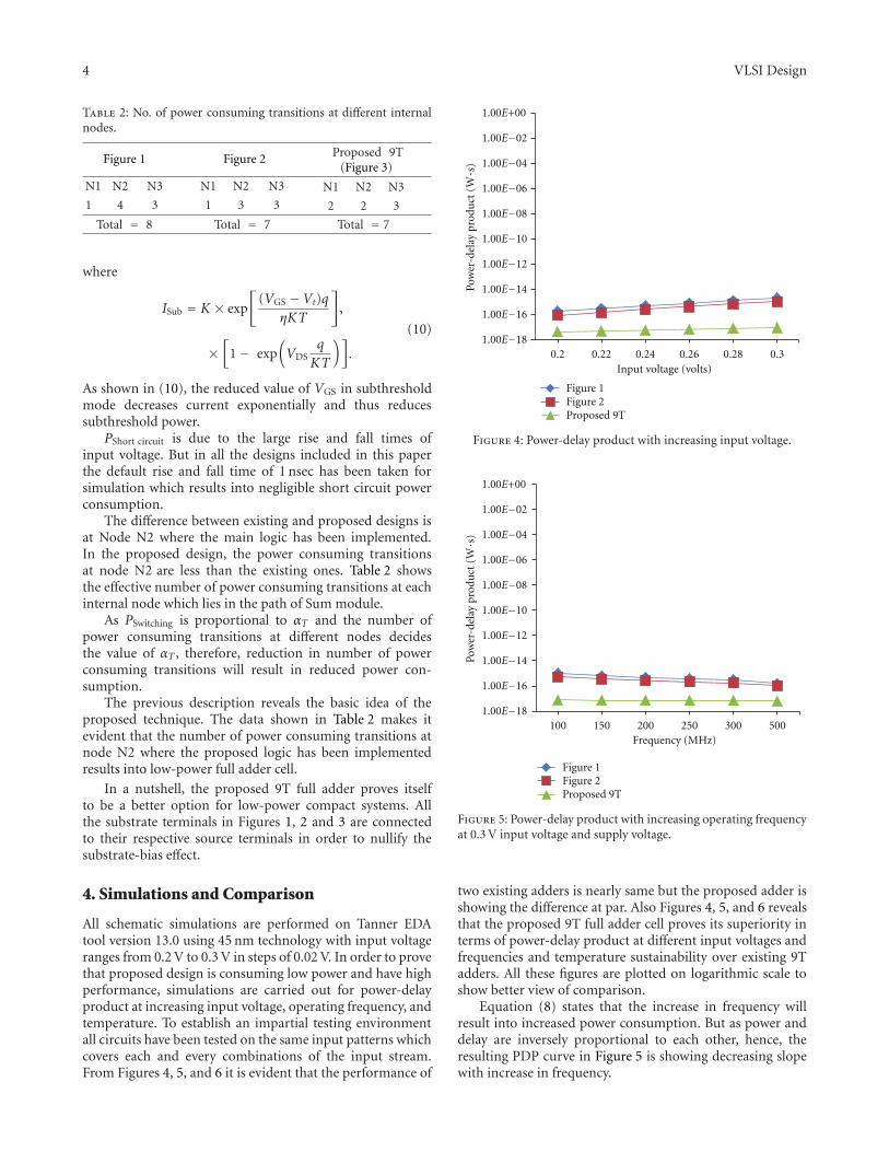
The difference between existing and proposed designs isat Node N2 where the main logic has been implemented.In the proposed design, the power consuming transitionsat node N2 are less than the existing ones. Table 2 showsthe effective number of power consuming transitions at eachinternal node which lies in the path of Sum module.
As PSwitching is proportional to αT and the number ofpower consuming transitions at different nodes decidesthe value of αT , therefore, reduction in number of powerconsuming transitions will result in reduced power con-sumption.
The previous description reveals the basic idea of theproposed technique. The data shown in Table 2 makes itevident that the number of power consuming transitions atnode N2 where the proposed logic has been implementedresults into low-power full adder cell.
In a nutshell, the proposed 9T full adder proves itselfto be a better option for low-power compact systems. Allthe substrate terminals in Figures 1, 2 and 3 are connectedto their respective source terminals in order to nullify thesubstrate-bias effect.
4. Simulations and Comparison
All schematic simulations are performed on Tanner EDAtool version 13.0 using 45 nm technology with input voltageranges from 0.2 V to 0.3 V in steps of 0.02 V. In order to provethat proposed design is consuming low power and have highperformance, simulations are carried out for power-delayproduct at increasing input voltage, operating frequency, andtemperature. To establish an impartial testing environmentall circuits have been tested on the same input patterns whichcovers each and every combinations of the input stream.From Figures 4, 5, and 6 it is evident that the performance of
Input voltage (volts)
Figure 1 Figure 2 Proposed 9T
1.00E+00
1.00E−02
1.00E−04
1.00E−06
1.00E−08
1.00E−10
1.00E−12
1.00E−14
1.00E−16
1.00E−18
Pow
er-d
elay
pro
duct
(W·s)
0.2 0.22 0.24 0.26 0.28 0.3
Figure 4: Power-delay product with increasing input voltage.
Frequency (MHz)
Figure 1 Figure 2 Proposed 9T
100 150 200 250 300 500
1.00E+00
1.00E−02
1.00E−04
1.00E−06
1.00E−08
1.00E−10
1.00E−12
1.00E−14
1.00E−16
1.00E−18
Pow
er-d
elay
pro
duct
(W·s)
Figure 5: Power-delay product with increasing operating frequencyat 0.3 V input voltage and supply voltage.
two existing adders is nearly same but the proposed adder isshowing the difference at par. Also Figures 4, 5, and 6 revealsthat the proposed 9T full adder cell proves its superiority interms of power-delay product at different input voltages andfrequencies and temperature sustainability over existing 9Tadders. All these figures are plotted on logarithmic scale toshow better view of comparison.
Equation (8) states that the increase in frequency willresult into increased power consumption. But as power anddelay are inversely proportional to each other, hence, theresulting PDP curve in Figure 5 is showing decreasing slopewith increase in frequency.

VLSI Design 5
Figure 1 Figure 2 Proposed 9T
−10 0 20 40 50 60Temperature (◦C)
1.00E+00
1.00E−02
1.00E−04
1.00E−06
1.00E−08
1.00E−10
1.00E−12
1.00E−14
1.00E−16
1.00E−18
Pow
er-d
elay
pro
duct
(W·s)
Figure 6: Power-delay product with varying temperature at 0.3 Vinput voltage and supply voltage.
The increase in temperature results into increase carriermobility, and due to this random motion of electrons andholes will increase and hence more number of electron holepairs will be formed in the interfacial region of the MOSFETthereby leading to delay in channel formation and incrementin threshold voltage. This increment in threshold voltage willgive rise to the power consumption of the device.
Also in a MOSFET, a pn junction is formed betweenthe Drain/Source and Bulk of the transistor. The currentequation of a pn-junction is expressed as
I = I0
�eqV/KT − 1
�. (11)
This states that with increase in temperature, current in-creases exponentially and results into more power consump-tion. This is the cause of slight rise in the curve of Figure 6with increasing temperature.
5. Conclusion
Based on the subthreshold conduction region, the designingof a 1-bit full adder has been done. The proposed 9T 1-bit fulladder is found to give better performance than both existing9T full adders in subthreshold region. The proposed circuithas been tested to have better temperature sustainabilityand significantly less power delay product to achieve highperformance. The proposed 9T adder has been designed andstudied using 45 nm technology and can be a viable optionfor low-power complex circuit design.
References
[1] N. Weste and K. Eshraghian, Principles of CMOS DigitalDesign, A System Perspective, Addisonn Wesley, Massachusetts,Mass, USA, 1993.
[2] S. Kang and Y. Leblebici, CMOS Digital Integrated CircuitAnalysis and Design, McGraw-Hill, 3rd edition, 2005.
[3] D. Sinha, T. Sharma, K. G. Sharma, and B. P. Singh, “Ultralow power 1-bit full adder,” International Journal of ComputerApplications, vol. 1, article 3, 2011.
[4] T. Sharma, K.G. Sharma, and B. P. Singh, “Low power and highperformance 1-bit 9T full adder,” in Proceedings of the i- COSTElectronics & Communication Conference, pp. 5.2.1–5.2.3, B. S.Deore College of Engineering, Dhule, January 2011.
[5] D. Sinha, T. Sharma, K. G. Sharma, and B. P. Singh, “Energyefficient design and analysis of 1-bit full adder cell,” Interna-tional Journal of Recent Trends in Engineering & Technology,vol. 5, no. 2, pp. 49–52, 2011.
[6] S. R. Chowdhury, A. Banerjee, A. Roy, and H. Saha, “A highspeed 8-transistor full adder design using novel 3 transistorXOR gates,” International Journal of Electronics, Circuits andSystems, vol. 2, no. 4, pp. 217–223, 2008.
[7] S. Veeramachaneni and M. B. Srinivas, “New improved 1-bitfull adder cells,” in Proceedings of the CCECE/ CCGEI, pp. 735–738, Niagara Falls, Canada, May 2008.
[8] D. Wang, M. Yang, W. Cheng, X. Guan, Z. Zhu, and Y.Yang, “Novel low power full adder cells in 180 nm CMOStechnology,” in Proceedings of the 4th IEEE Conference onIndustrial Electronics and Applications (ICIEA ’09), pp. 430–433, May 2009.
[9] T. Sharma, K. G. Sharma, B. P. Singh, and N. Arora, “Anovel CMOS 1-bit 8T full adder cell,” WSEAS Transactions onSystems, vol. 9, no. 3, pp. 317–326, 2010.
[10] M. Hosseinghadiry, M. Mohammadi, and M. Nadisenejani,“Two new low power high performance full adders with min-imum gates,” International Journal of Electrical and ComputerEngineering, vol. 4, pp. 671–678, 2009.
International Journal of Computer Engineering and Technology (IJCET), ISSN 0976 – 6367(Print),
ISSN 0976 – 6375(Online) Volume 3, Issue 1, January- June (2012), © IAEME
76
NEW DESIGN OF LOW POWER 3T XOR CELL
1Shiwani Singh,
2Tripti Sharma
*,
2K. G. Sharma and
1Prof. B. P. Singh
1Electronics and Communication Department
FET- MITS (Deemed University)
Lakshmangarh, Distt.- Sikar, India 2Electronics and Communication Department
Suresh Gyan Vihar University, Jagatpura
Jaipur, Rajasthan, India
E-mail: [email protected],
ABSTRACT
This paper proposes a 3T XOR gate design implemented using pMOS transistors
only. The design has been compared with existing design and significant
improvement in power consumption has been obtained. All pre layout simulations
are performed on 45nm standard model on Tanner EDA tool version 13.0.
KeywordXOR gate, low power and pMOS transistor
I. INTRODUCTION
The XOR gate forms the basic building blocks of various digital VLSI circuits like
full adder, multiplier, comparator and parity checker. Enhancing the performance
of the XOR gates can significantly improve the performance of the system as
whole. The design of this gate has been undergoing a considerable improvement in
terms of power consumption. Many design architectures and techniques have been
developed to reduce power consumption and has become one of the primary
focuses of digital design [1]. This paper proposes a 3T XOR circuit which reduces
INTERNATIONAL JOURNAL OF COMPUTER ENGINEERING &
TECHNOLOGY (IJCET)
ISSN 0976 – 6367(Print) ISSN 0976 – 6375(Online)
Volume 3, Issue 1, January- June (2012), pp. 76-80
© IAEME: www.iaeme.com/ijcet.html Journal Impact Factor (2011): 1.0425 (Calculated by GISI)
www.jifactor.com
IJCET
© I A E M E

International Journal of Computer Engineering and Technology (IJCET), ISSN 0976 – 6367(Print),
ISSN 0976 – 6375(Online) Volume 3, Issue 1, January- June (2012), © IAEME
77
the threshold-loss problem significantly as exists in previous designs and improves
the power consumption too.
The paper is organized as follows: Section II describes an existing 3T XOR cell as
reported in the literature. Section III introduces the proposed 3T XOR cell.
Simulation results and their comparisons are included in Section IV and finally
Section V concluded the paper.
II. Prior Work
Figure 1 Existing XOR Gate
The design shown in Fig.1 [2]-[6] is based on a modified version of a CMOS
inverter and a pMOS pass transistor. When the input B is at logic high, the inverter
functions like a normal CMOS inverter. When the input B is at logic low, the
CMOS inverter output is at high impedance. However, the pass transistor M3 is
enabled and the output Y gets the same logic value as input A. However, when
A=1 and B=0, voltage degradation due to threshold drop occurs across transistor
M3 and consequently the output Y is degraded with respect to the input. The
voltage degradation due to threshold drop can be considerably minimized by
increasing the W/L ratio of transistor M3 [7]. Table I illustrates the performance in
terms of obtained output at various input combinations.
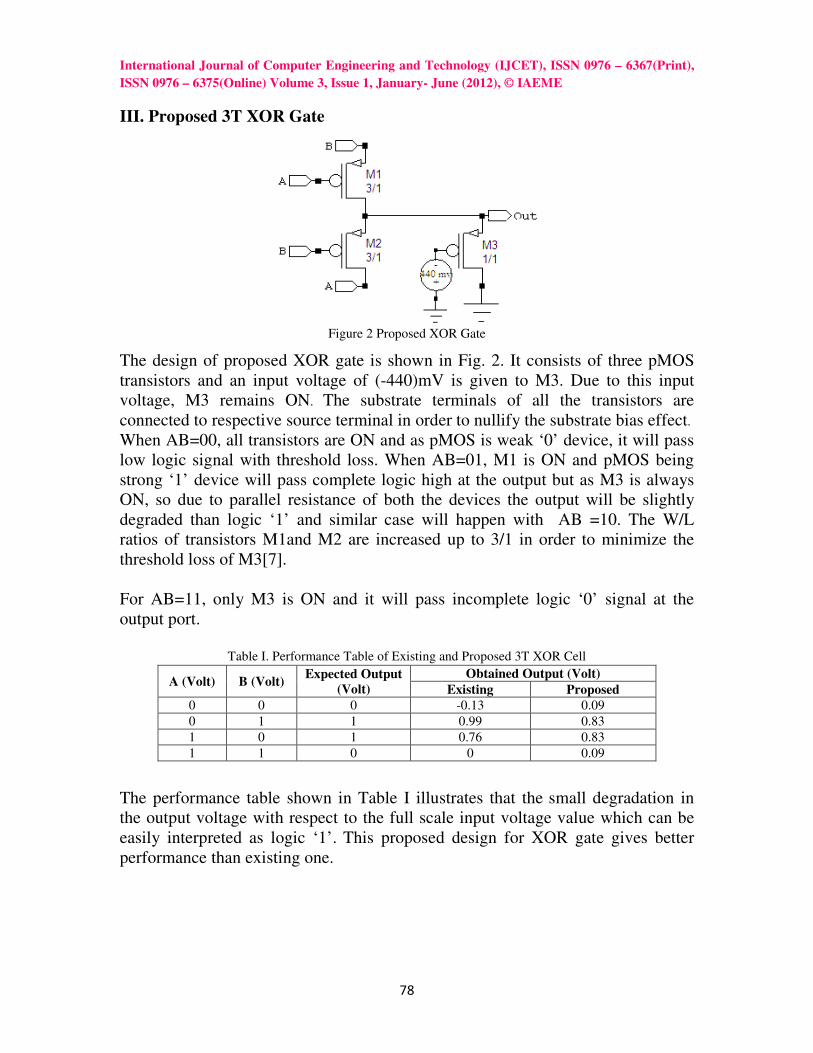
International Journal of Computer Engineering and Technology (IJCET), ISSN 0976 – 6367(Print),
ISSN 0976 – 6375(Online) Volume 3, Issue 1, January- June (2012), © IAEME
78
III. Proposed 3T XOR Gate
Figure 2 Proposed XOR Gate
The design of proposed XOR gate is shown in Fig. 2. It consists of three pMOS
transistors and an input voltage of (-440)mV is given to M3. Due to this input
voltage, M3 remains ON. The substrate terminals of all the transistors are
connected to respective source terminal in order to nullify the substrate bias effect.
When AB=00, all transistors are ON and as pMOS is weak ‘0’ device, it will pass
low logic signal with threshold loss. When AB=01, M1 is ON and pMOS being
strong ‘1’ device will pass complete logic high at the output but as M3 is always
ON, so due to parallel resistance of both the devices the output will be slightly
degraded than logic ‘1’ and similar case will happen with AB =10. The W/L
ratios of transistors M1and M2 are increased up to 3/1 in order to minimize the
threshold loss of M3[7].
For AB=11, only M3 is ON and it will pass incomplete logic ‘0’ signal at the
output port.
Table I. Performance Table of Existing and Proposed 3T XOR Cell
The performance table shown in Table I illustrates that the small degradation in
the output voltage with respect to the full scale input voltage value which can be
easily interpreted as logic ‘1’. This proposed design for XOR gate gives better
performance than existing one.
A (Volt) B (Volt) Expected Output
(Volt)
Obtained Output (Volt)
Existing Proposed
0 0 0 -0.13 0.09
0 1 1 0.99 0.83
1 0 1 0.76 0.83
1 1 0 0 0.09
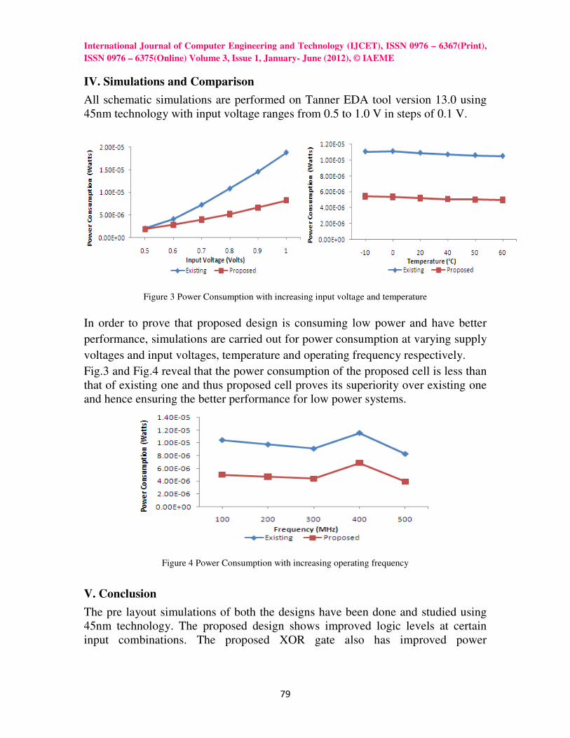
International Journal of Computer Engineering and Technology (IJCET), ISSN 0976 – 6367(Print),
ISSN 0976 – 6375(Online) Volume 3, Issue 1, January- June (2012), © IAEME
79
IV. Simulations and Comparison
All schematic simulations are performed on Tanner EDA tool version 13.0 using
45nm technology with input voltage ranges from 0.5 to 1.0 V in steps of 0.1 V.
Figure 3 Power Consumption with increasing input voltage and temperature
In order to prove that proposed design is consuming low power and have better
performance, simulations are carried out for power consumption at varying supply
voltages and input voltages, temperature and operating frequency respectively.
Fig.3 and Fig.4 reveal that the power consumption of the proposed cell is less than
that of existing one and thus proposed cell proves its superiority over existing one
and hence ensuring the better performance for low power systems.
Figure 4 Power Consumption with increasing operating frequency
V. Conclusion
The pre layout simulations of both the designs have been done and studied using
45nm technology. The proposed design shows improved logic levels at certain
input combinations. The proposed XOR gate also has improved power

International Journal of Computer Engineering and Technology (IJCET), ISSN 0976 – 6367(Print),
ISSN 0976 – 6375(Online) Volume 3, Issue 1, January- June (2012), © IAEME
80
consumption with respect to various parameters. Hence, the proposed gate can be
used for various applications like adder, multiplier and other complex designs.
REFERENCES
1. Y. Leblebici, S.M. Kang (1999), “CMOS Digital Integrated Circuits,”
Singapore: McGraw Hill, 2nd edition, Ch. 7.
2. T.Sharma, et. al. (2010), “High Speed, Low Power 8T Full Adder Cell with
45% Improvement in Threshold Loss Problem,” Proceedings of the 12th
International Conference on Networking, VLSI and Signal Processing, pp. 272-
276, Coimbatore and University of Cambridge, UK.
3. Tripti Sharma, et. al. (2010),, “A Novel CMOS 1-bit 8T Full Adder Cell,”
World Scientific and Engineering Academy and Society (WSEAS) Transactions
on Systems, Vol. 9, No.3, pp.317-32.
4. Tripti Sharma, et. al.(2010), “High Performance Full Adder Cell: A
Comparative Analysis,” Proceedings of the 2010 IEEE Student’s Technology
Symposium, 3-4 April, IIT Kharagpur.
5. S. R. Chowdhury, et. al.(2008), “ A high speed 8-transistor full adder design
using novel 3 transistor XOR gates,” International Journal of Electronics,
Circuits and Systems, vol. 2, No. 4, pp. 217-223.
6. J. Wang, et. al.(1994), “New efficient designs for XOR and XNOR functions on
the transistor level,” IEEE J. Solid-State Circuits, vol. 29, no. 7, pp. 780–786.
7. Y.Tsividis, (1996), “Mixed Analog-Digital VLSI Devices and Technology,”
Singapore: McGraw Hill, 1st edition.

International Journal of Computer Applications (0975 – 8887) Volume 42– No.15, March 2012
6
PMOS based 1-Bit Full Adder Cell
1Shiwani Singh, 2Tripti Sharma, 2K. G. Sharma and 1Prof. B. P. Singh
1FET- MITS(Deemed University) Lakshmangarh-332311
Rajasthan, INDIA 2Suresh Gyan Vihar University
Jagatpura, Jaipur Rajasthan, INDIA
ABSTRACT This paper presents post layout simulations of a new 8T full adder cell using a new 3T XOR gate implemented by pMOS transistors only. This proposed design operates efficiently in super threshold region to achieve ultra low power and hence reduced power-delay product (PDP). The proposed design demonstrates its superiority against existing adder in terms of power–delay product, temperature sustainability and noise immunity. It also shows remarkable improvement in threshold loss as compared to existing 8T full adder for certain input combinations. Therefore, the proposed design outperforms the existing adder and proves to be an optimal option for low power and energy efficient applications. All the post-layout simulations have been performed at 45nm technology on Tanner EDA tool version 13.0.
Keywords 3T, 8T, full adder, PDP and XOR.
1. INTRODUCTION Low power has emerged as a principal theme in today‟s electronics industry. The need for low power has caused a major paradigm shift where power dissipation has become as important a consideration as performance and area [1] and [2]. Addition is one of the fundamental arithmetic operations. It is used extensively in many VLSI systems such DSP architectures, microprocessors, etc. In addition to its main task which is adding two binary numbers, it is the nucleus of many other useful operations such as subtraction, multiplication, division, etc. So, it is very important to choose the adder topology that would yield the desired performance. That‟s why, building low-power, high performance adder cells are of great interest and any modifications made to the full adder would affect the system as a whole. IC Layout or mask design is the representation of an integrated circuit in terms of planar geometric shapes which correspond to the patterns of metal, oxide, or semiconductor layers that make up the components of the integrated circuit. In other words, Layout is the process by which a circuit specification is converted to a physical implementation with enough information to deduce all the relevant physical parameters of the circuit. The paper is organized as follows: Section 2 describes an existing 8T full adder cell as reported in the literature. Section3 introduces the proposed 3t XOR cell and 8T full adder
design. Simulation results and their comparisons are included in Section 4 and finally Section 5 concluded the paper.
2. PREVIOUS WORK The full adder operation can be stated as follows: Given the three 1-bit inputs A, B, and Cin, it is desired to calculate the two 1-bit outputs Sum and Carry, where
Sum = (A ⨁ B) ⨁ Cin (1) Cout = AB + Cin (A ⨁ B) (2)
Fig 1: Schematic of 1-bit 8T Full Adder
Fig. 1 shows the schematic of eight transistor (8T) 1-bit full adder cell. The Sum output is basically obtained by a cascaded exclusive ORing using 3T XOR gate [3] of the three inputs. Cout is implemented using 2T multiplexer. Fig. 2 shows the layout design of 1-bit 8T full adder.
Fig 2: Layout of 1-bit 8T Full Adder
In the design of Fig.1 two stage delays are required to obtain the Sum output and at most two stage delays are required to obtain the carry output Cout[4]-[7]. It has serious threshold loss for inputs are 000, 010, 100 and 110 due to simultaneous

International Journal of Computer Applications (0975 – 8887) Volume 42– No.15, March 2012
7
enabling of two transistors. Logic high output at first stage of XOR gate enables M4 and Cin =0 enables M6 and similarly, logic low output at first stage of XOR gate enables M5 and Cin =0 enables M6. Thus, Sum output is degraded due to reduced device resistance as the ON transistors will have combined parallel effect on resistance. The outputs have good logic level for only four input vectors. For the remaining input vectors, there is a major degradation in output voltage that may lead to functional failure as well as increased power consumption. As the voltage is scaled down, the signal integrity deteriorates and the speed decreases tremendously.
3. PROPOSED 3T XOR CELL AND 8T FULL ADDER DESIGN
Fig 3: Schematic of proposed 3T XOR cell
The design of full adder is based on the design of the XOR gate. The schematic of new 3T XOR cell is shown in Fig. 3. It consists of 3 pMOS transistors and an negative input supply voltage of 250 mV is given to M3 so that it conducts in weak inversion and eliminates the negative voltage spikes for input combination „00‟. The W/L ratios of transistors M1and M2 are taken as 3/1 to minimize the voltage drop due to the threshold loss in transistors. When AB=00, all transistors are ON and as pMOS is weak „0‟ device, it will pass low logicsignal with threshold loss. When AB=01, M1 is ON and pMOS being strong „1‟ device will pass complete logic high at the output but as M3 is always ON, so due to parallel resistance of both the devices the output will be slightly degraded than logic „1‟ and similar case will happen with AB =10. For AB=11, only M3 is ON and pMOS is weak „0‟ device, it will pass low logic signal with threshold loss.The substrate terminals of all the transistors are connected to respective source terminal in order to nullify the substrate bias effect. This proposed design for XOR gate gives better performance than existing one. Table 1 states the performance of both the designs.
Table 1. Performance Table of Existing and Proposed 3T
XOR cell
A (Volt) B (Volt) Expected Output (Volt)
Obtained Output (Volt)
Existing Proposed 0 0 0 -0.13 0.02 0 1 1 0.99 0.84 1 0 1 0.76 0.84 1 1 0 0 0.02
Using this XOR gate an 8T adder has also been realized. Fig. 4 and Fig. 5 shows the schematic and layout design of proposed 8T full adder cell design. In this, Sum module has been implemented using cascaded 3T XOR gate in accordance with equations (1) and (2) and Cout module is designed by using 2T multiplexer.
Fig 4: Schematic of proposed 8T full adder
Fig 5: Layout Design of Proposed Full Adder cell
Table 2. Performance Table of Existing and Proposed 8T Full adder cell
A B Cin Sum (Existing) Sum (Proposed)
0 0 0 <<│VTp│ 2% of logic “0”
0 0 1 1 90% of logic “1”
0 1 0 50% of logic “1” 70% of logic “1”
0 1 1 0 6% of logic “0”
1 0 0 50% of logic “1” 70% of logic “1”
1 0 1 0 6% of logic “0”
1 1 0 <<│VTp│ 2% of logic “0”
1 1 1 1 90% of logic “1” This proposed design shows small voltage drop for certain input combinations but this drop is so less that it can be
assumed as logic high. Table 1 depicts the performance of both the designs. For inputs „000‟, all transistors are ON and

International Journal of Computer Applications (0975 – 8887) Volume 42– No.15, March 2012
8
as pMOS is weak „0‟ device, it will pass low logic signal with threshold loss. For 010, M1 is ON and pMOS being strong „1‟ device will pass complete logic high at the output but as M3 is always ON, so due to parallel resistance of both the devices the output will be slightly degraded than logic „1‟. Logic high output at first stage XOR will be passed through M4 but since M6 is always ON, so due to parallel resistance of both the devices the output will be slightly degraded than logic „1‟and similar case will happen with AB =100. It is evident from Table 2 depicts that the proposed design has improved threshold loss as compared to existing one.
4. SIMULATIONS AND COMPARISON All post layout simulations are performed on Tanner EDA tool version 13.0 using 45nm technology with input voltage ranges from 0.5 to 1.0 V in steps of 0.1 V. In order to prove that the proposed design is consuming low power and have better performance, simulations are carried out for power consumption and delay and as a result the overall PDP at varying input voltages and temperature has been estimated. Also to ensure the better noise immunity of the proposed design, output noise voltages have been extracted at varying frequency. To establish an impartial testing environment both circuit have been tested on the same input patterns which covers all combinations of the input stream. After the physical layout designing post-layout simulations are carried out with extraction of parasitic capacitances. Power consumption is a function of load capacitance therefore any reduction in capacitance will lead to reduced power consumption. Table 3 shows significant improvement in total as well as output parasitic capacitance of the proposed full adders over existing one.
Table 3. Parasitic Capacitance of existing and proposed full adder cells
Full Adder Cells
Parasitic Capacitance (fF)
Total Output
Existing 0.822 0.185
Proposed 0.564 0.125
The proposed design of full adder cell has remarkably less parasitic capacitance than existing design and hence, as power consumption is directly proportional to capacitance, thereforeproposed design will also have remarkable reduction in power consumption. Also, both the adders has been implemented with same logic of cascading XOR gate therefore both have equal number of power consuming transitions at all the nodes and as a result switching activity will remain constant for both the adder designs. In the layout design of the proposed full adder cell, number of poly contacts is four and in existing designs it is seven. The number of overlaps is also less in proposed design. Thus, this leads to the improved power consumption of proposed design than the existing adder. The results for the same are shown in Fig. 6- Fig. 8. Fig. 6 depicts the superiority of proposed 8T full adder in terms of PDP with varying input voltage. Fig. 7 reveals the better performance of proposed design over existing one. As the proposed cell is implemented using pMOS transistors only, therefore, the power consumption will decrease with increasing temperature and hence the PDP.
Fig 6: PDP vs input voltage
Fig 7: PDP vs varying temperature at 0.6 input voltage
Fig 8: Output noise voltage with operating frequency
This is due to NBTI effect [8] which demonstrates the negative shift of threshold voltage caused by variation in temperature. Also the Fermi potential of the pMOS reduceswith increase in temperature [9] and as a result the device threshold voltage will also decrease. On the other hand, power consumption is dependent on threshold voltage and hence it will also reduce as shown in Fig.7. Also, the noise immunity of proposed cell is remarkably better than existing one as shown in Fig.8. Therefore, the proposed adder can be a better
0.00E+00
1.00E14
2.00E14
3.00E14
4.00E14
5.00E14
6.00E14
0.5 0.6 0.7 0.8 0.9 1
Power-Delay Product (Watt-sec)
Input Voltage (Volt)
Existing Proposed
0.00E+00
1.00E14
2.00E14
3.00E14
4.00E14
5.00E14
6.00E14
10 0 20 40 50 60
Power-Delay Product (Watt-sec)
Temperature (°C)
Existing Proposed
1.00E05
1.00E04
1.00E03
1.00E02
1.00E01
1.00E+00
1.2 2.3 3.4 4.5 5.6 6.7 7.8 8.9 10
Output Noise Voltage (Volt)
Frequency (MHz)
Existing Proposed

International Journal of Computer Applications (0975 – 8887) Volume 42– No.15, March 2012
9
option for complex system design such as ripple carry adder, array multiplier etc. The graphs based on post-layout simulations shown in Fig. 6-Fig. 8 results into the better performance of proposed design in comparison to existing design. 5. CONCLUSION The proposed 8T full adder cell has been designed using a new 3T XOR cell implemented by pMOS transistors only. Schematic and layout of both the adder circuits in this paper have been designed and simulated using 45nm technology. The PDP of proposed circuit is remarkably improved with respect to increasing input voltage as well as temperature. Also the parasitic extracted and the output noise voltage simulated is better than the existing design. Hence in a nutshell the proposed adder proves itself to be a better option for low power devices and systems design than its peer design.
6. REFERENCES [1] N. Weste and K. Eshraghian, Principles of CMOS
VLSI Design, A System Perspective. Reading, MA: Addison-Wesley, 1993.
[2] S. Kang and Y. Leblebici, CMOS Digital Integrated Circuits, Analysis and Design, 3rd ed.
[3] S. R. Chowdhury, A. Banerjee, A. Roy, H. Saha, “ A high speed 8-transistor full adder design using novel 3 transistor XOR gates,” International Journal of Electronics, Circuits and Systems, vol. 2, No. 4, pp. 217-223, 2008.
[4] T. Sharma, K.G.Sharma, Prof.B.P.Singh, Neha Arora, “A Novel CMOS 1-bit 8T Full Adder Cell,” in World Scientific and Engineering Academy and Society (WSEAS) Transactions on Systems, vol. 9, No.3, pp. 317-326, March 2010.
[5] D.Wang, M.Yang, W.Cheng, X.Guan, Z.Zhu, Y.Yang, “Novel Low Power Full Adder Cells in 180nm CMOS Technology,” in Prod.IEEE ICIEA, pp. 430-433, 2009.
[6] S.Veeramachaneni, M.B.Srinivas, “New Improved 1-Bit Full Adder Cells,” CCECE/ CCGEI, Niagara Falls. Canada, pp. 735-738, May 5-7 2008.
[7] T. Sharma, K. G. Sharma and Prof. B. P. Singh, “Energy Efficient 1-bit Full Adder Cell with 45% Reduced Threshold Loss,” International Journal of Recent Trends in Engineering, vol 3, pp.106-110, 2010.
[8] Austin Lesea and Andrew Percey” Negative-Bias Temperature Instability (NBTI) Effects in 90 nm PMOS” XilinxWP224 (v1.1) November 21, 2005.
[9] Michael S-C Lu1, Dong-Hang Liu, Li-Sheng Zheng and Sheng-Hsiang Tseng “CMOS micromachined structures using transistors in the subthreshold region for thermal sensing”, Journal of micromechanics and microengineering, 2006 pp. 1734-1739.