UCC28782 Practical Design Guidelines
14
Application Note UCC28782 Practical Design Guidelines ABSTRACT This application note provides system design guidelines for UCC28782 ACF controller. The process for optimizing certain ACF design parameters such as ACF and IC key function introduction and design SOP, check list, and transformer design. The application note also provides several useful tools and reference designs, to refer these document to design UCC28782 easily. Table of Contents 1 Introduction............................................................................................................................................................................. 2 2 Control Law across Entire Load Range................................................................................................................................ 3 3 Design SOP and Checklist..................................................................................................................................................... 5 4 Practical IC Pin Setting...........................................................................................................................................................7 4.1 BUR Pin (Programmable Burst Mode)............................................................................................................................... 7 4.2 RDM Pin (Sets Synthesized Demagnetization Time for ZVS Tuning)................................................................................ 8 4.3 RTZ Pin (Sets Delay for Transition Time to Zero).............................................................................................................. 9 4.4 Boost Pin ......................................................................................................................................................................... 11 5 Transformer design.............................................................................................................................................................. 12 6 References............................................................................................................................................................................ 13 List of Figures Figure 1-1. Simplified Type Circuit............................................................................................................................................... 2 Figure 2-1. Control Law Over Entire Load Range Based on the V VS Condition as V IPC < 0.9 V................................................. 3 Figure 2-2. Control Law Under Different Load Sweep Direction as V IPC > 0.9 V and V VS > V VSLV(UP) ....................................... 4 Figure 4-1. Hysteresis Voltage Generation on BUR Pin.............................................................................................................. 7 Figure 4-2. SR VDS spike during first high side turn on.............................................................................................................. 8 Figure 4-3. RTZ Setting for the Falling-edge Transition of VSW................................................................................................. 9 Figure 4-4. RTZ Setting too large cause VDS ring back............................................................................................................ 10 Figure 4-5. Boost Circuit............................................................................................................................................................ 11 List of Tables Table 2-1. Functional Modes........................................................................................................................................................3 Table 3-1. Schematic Checklist....................................................................................................................................................6 Table 3-2. Layout Checklist..........................................................................................................................................................6 Trademarks All trademarks are the property of their respective owners. www.ti.com Table of Contents SLUAAG2 – OCTOBER 2021 Submit Document Feedback UCC28782 Practical Design Guidelines 1 Copyright © 2021 Texas Instruments Incorporated
Transcript of UCC28782 Practical Design Guidelines
Application NoteUCC28782 Practical Design Guidelines
ABSTRACT
This application note provides system design guidelines for UCC28782 ACF controller. The process for optimizing certain ACF design parameters such as ACF and IC key function introduction and design SOP, check list, and transformer design. The application note also provides several useful tools and reference designs, to refer these document to design UCC28782 easily.
Table of Contents1 Introduction.............................................................................................................................................................................22 Control Law across Entire Load Range................................................................................................................................33 Design SOP and Checklist.....................................................................................................................................................54 Practical IC Pin Setting...........................................................................................................................................................7
4.1 BUR Pin (Programmable Burst Mode)............................................................................................................................... 74.2 RDM Pin (Sets Synthesized Demagnetization Time for ZVS Tuning)................................................................................84.3 RTZ Pin (Sets Delay for Transition Time to Zero).............................................................................................................. 94.4 Boost Pin ......................................................................................................................................................................... 11
5 Transformer design.............................................................................................................................................................. 126 References............................................................................................................................................................................ 13
List of FiguresFigure 1-1. Simplified Type Circuit...............................................................................................................................................2Figure 2-1. Control Law Over Entire Load Range Based on the VVS Condition as VIPC < 0.9 V................................................. 3Figure 2-2. Control Law Under Different Load Sweep Direction as VIPC > 0.9 V and VVS > VVSLV(UP) .......................................4Figure 4-1. Hysteresis Voltage Generation on BUR Pin.............................................................................................................. 7Figure 4-2. SR VDS spike during first high side turn on.............................................................................................................. 8Figure 4-3. RTZ Setting for the Falling-edge Transition of VSW................................................................................................. 9Figure 4-4. RTZ Setting too large cause VDS ring back............................................................................................................10Figure 4-5. Boost Circuit............................................................................................................................................................ 11
List of TablesTable 2-1. Functional Modes........................................................................................................................................................3Table 3-1. Schematic Checklist....................................................................................................................................................6Table 3-2. Layout Checklist..........................................................................................................................................................6
TrademarksAll trademarks are the property of their respective owners.
www.ti.com Table of Contents
SLUAAG2 – OCTOBER 2021Submit Document Feedback
UCC28782 Practical Design Guidelines 1
Copyright © 2021 Texas Instruments Incorporated
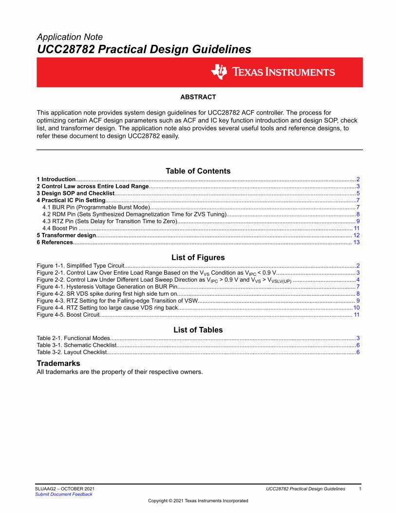
1 IntroductionThe UCC28782 is a transition-mode (TM) active clamp flyback (ACF) controller, equipped with advanced control schemes, to enable significant size reduction of passive components, for higher power density and higher average efficiency. The control law is optimized for Silicon (Si) and Gallium Nitride (GaN) power FETs in a half-bridge configuration and is capable of driving high-frequency AC/DC converters up to 1.5 MHz. The zero voltage switching (ZVS) control of the UCC28782 is capable of auto-tuning the on-time of a high-side clamp switch (QH) by using a unique loss less ZVS sensing network connected between the switch-node voltage (VSW) and SWS pin. The ACF controller is designed to adaptively achieve targeted full-ZVS or partial-ZVS conditions for the low-side main switch (QL) with minimum circulating energy over wide operating conditions. Auto-tuning eliminates the risk of losing ZVS due to component tolerance, input/output voltage changes, and temperature variations, since the QH on-time is corrected cycle-by-cycle.
Figure 1-1. Simplified Type Circuit
Introduction www.ti.com
2 UCC28782 Practical Design Guidelines SLUAAG2 – OCTOBER 2021Submit Document Feedback
Copyright © 2021 Texas Instruments Incorporated
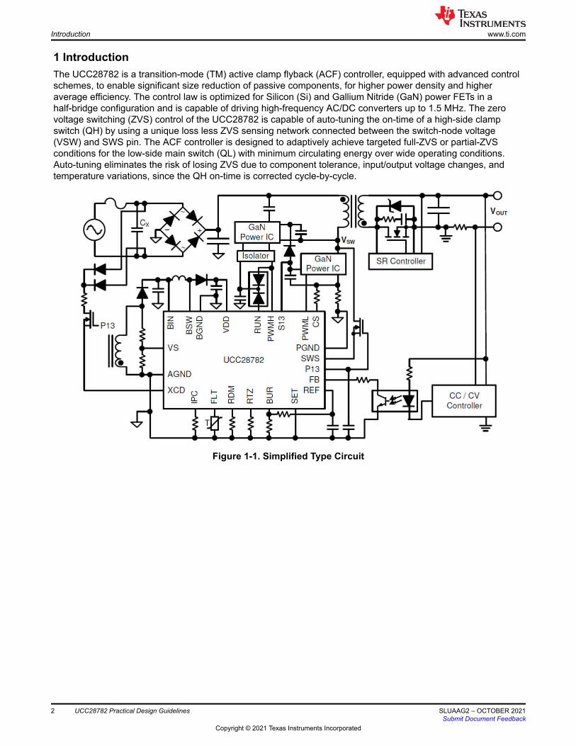
2 Control Law across Entire Load RangeUCC28782 contains six modes of operation summarized in Table 2-1. Starting from heavier load, the AAM mode forces PWML and PWMH into complementary switching with ZVS tuning enabled. ABM mode generates a group of PWML and PWMH pulses as a burst packet, and adjusts the burst off-time to regulate the output voltage. At the same time, the burst frequency variation is confined above 20kHz by adjusting the number of PWML and PWMH pulses per packet to mitigate audible noise and reduce burst output ripple. In LPM, SBP1, and SBP2 modes, PWMH and the ZVS tuning loop are disabled, so the converter operates in valley-switching. The survival mode is to maintain VVDD higher than VVDD(OFF) in a long burst off time, and also performs the clamping capacitor balancing function to reduce the voltage stress of the secondary-side rectifier .
Table 2-1 and Figure 2-1 also show the frequency and power level at each mode, so it helps to understand the mode operation.
Table 2-1. Functional ModesMODE OPERATION PWMH ZVS
AAM Adaptive Amplitude Modulation ACF operation with PWML and PWMH in complementary switching
Enabled Yes
ABM Adaptive Burst Mode Variable FBUR > FBUR(LR), ACF operation in complementary switching
Enabled Yes
LPM Low Power Mode Fix FBUR ≈ FLPM, valley-switching Disabled No
SBP1 First Standby Power Mode Variable FBUR between FSBP2(LR) and FSBP2(UP), valley- switching
Disabled No
SBP2 Second Standby Power Mode Variable FBUR< FSBP2(UP) as VBUR < 0.9 V; Variable FBUR< FSBP2(LR) as VBUR > 0.9 V; Both are in valley-switching
Disabled No
INT_STOP Survival Mode When VVDD < VVDD(OFF) + VVDD(PCT), a series of PWML pulses followed by a long PWMH pulse is generated
Enabled in the lastswitching cycle of a survival-mode burst packet
No
Figure 2-1. Control Law Over Entire Load Range Based on the VVS Condition as VIPC < 0.9 V
www.ti.com Control Law across Entire Load Range
SLUAAG2 – OCTOBER 2021Submit Document Feedback
UCC28782 Practical Design Guidelines 3
Copyright © 2021 Texas Instruments Incorporated
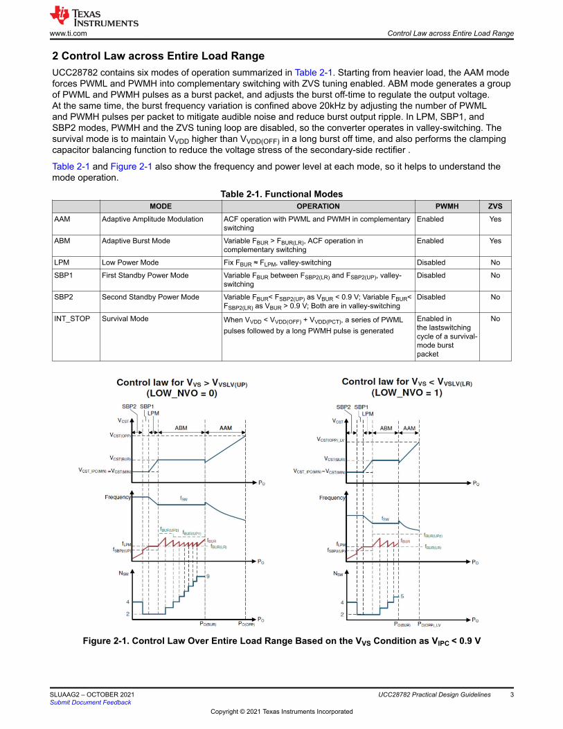
Figure 2-2. Control Law Under Different Load Sweep Direction as VIPC > 0.9 V and VVS > VVSLV(UP)
Control Law across Entire Load Range www.ti.com
4 UCC28782 Practical Design Guidelines SLUAAG2 – OCTOBER 2021Submit Document Feedback
Copyright © 2021 Texas Instruments Incorporated
3 Design SOP and ChecklistTI has several publications and reference design to assist customers with designing the UCC28782. The following are some of the publications to assist with customer design.
Selecting the correct reference design as a starting point
• 65W ACF for PD application• 65W ZVS flyback for PD application• 100W PFC + ACF with Si-MOS application• 100W PFC + ACF with GaN application
Using calculator to design parameter
After choosing the correct reference design, the user can customize the parameter with their spec by calculator, UCC28782 calculator includes the IC parameter design and transformer design and secondary side resonance tuning and feedback loop design with TL431, so it is very helpful for customer to design the ACF board.
UCC28782 design calculator tool
Refer the layout guidelines with the data sheet section 11
When the schematic is completed, the layout can be started, the layout guidelines shown at data sheet section 11, and it includes general considerations and detail layout suggestion for each pin and layout example, it covers almost all layout suggestion with UCC28782. It is recommended to review before layout.
UCC28782 data sheet
Review the schematic and layout with checklist
The the schematic and layout design is completed, refer to the checklist shown in Table 3-1 and Table 3-2, so the user can double check that they did not miss any significant item.
UCC28782 system bring up guideline and debug FAQ
After the schematic and layout is finished, the user needs to evaluate the board, and might also face several issue. The user can refer to the application note for these item to speed up the debugging.
UCC28782 system timing up guideline and debug FAQ:
EMI filter design
After the system performance meets the spec without issue, the user needs to fine tune the EMI. TI has several application notes to assist with EMI tuning that include the following:
• Transformer structures that achieve low EMI with low and high side rectifiers• Flyback Transformer Design for Efficiency and EMI• Designing Low EMI Power Converters for Industrial and Automotive Systems• Input EMI Filter Design for Offline Phase-Dimmable LED Power Supplies
www.ti.com Design SOP and Checklist
SLUAAG2 – OCTOBER 2021Submit Document Feedback
UCC28782 Practical Design Guidelines 5
Copyright © 2021 Texas Instruments Incorporated
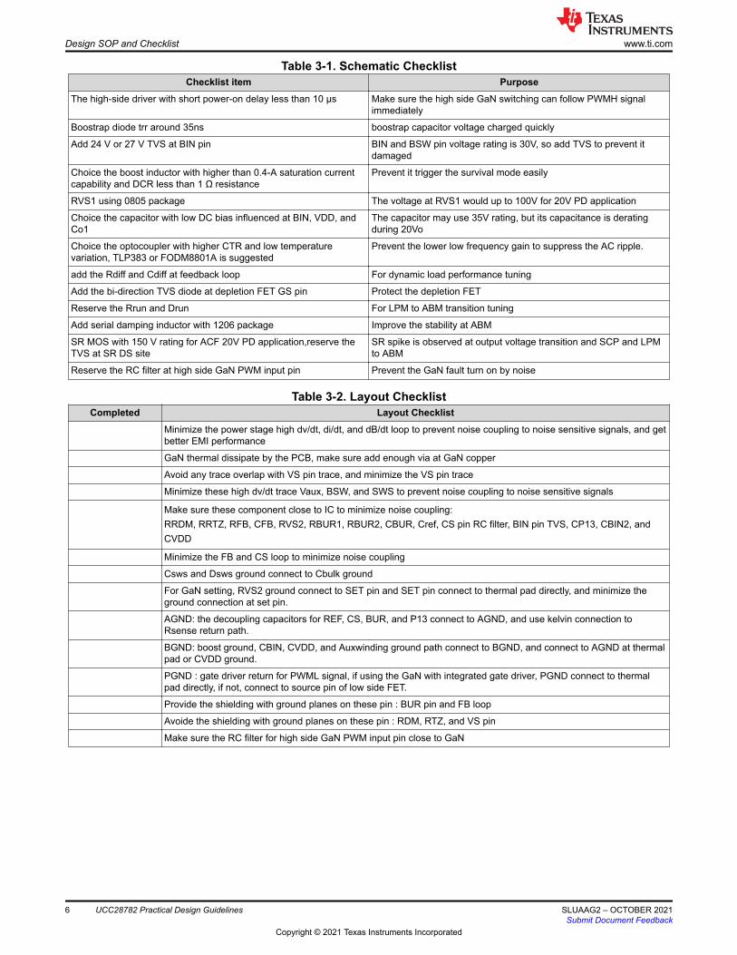
Table 3-1. Schematic ChecklistChecklist item Purpose
The high-side driver with short power-on delay less than 10 μs Make sure the high side GaN switching can follow PWMH signal immediately
Boostrap diode trr around 35ns boostrap capacitor voltage charged quickly
Add 24 V or 27 V TVS at BIN pin BIN and BSW pin voltage rating is 30V, so add TVS to prevent it damaged
Choice the boost inductor with higher than 0.4-A saturation current capability and DCR less than 1 Ω resistance
Prevent it trigger the survival mode easily
RVS1 using 0805 package The voltage at RVS1 would up to 100V for 20V PD application
Choice the capacitor with low DC bias influenced at BIN, VDD, and Co1
The capacitor may use 35V rating, but its capacitance is derating during 20Vo
Choice the optocoupler with higher CTR and low temperature variation, TLP383 or FODM8801A is suggested
Prevent the lower low frequency gain to suppress the AC ripple.
add the Rdiff and Cdiff at feedback loop For dynamic load performance tuning
Add the bi-direction TVS diode at depletion FET GS pin Protect the depletion FET
Reserve the Rrun and Drun For LPM to ABM transition tuning
Add serial damping inductor with 1206 package Improve the stability at ABM
SR MOS with 150 V rating for ACF 20V PD application,reserve the TVS at SR DS site
SR spike is observed at output voltage transition and SCP and LPM to ABM
Reserve the RC filter at high side GaN PWM input pin Prevent the GaN fault turn on by noise
Table 3-2. Layout ChecklistCompleted Layout Checklist
Minimize the power stage high dv/dt, di/dt, and dB/dt loop to prevent noise coupling to noise sensitive signals, and get better EMI performance
GaN thermal dissipate by the PCB, make sure add enough via at GaN copper
Avoid any trace overlap with VS pin trace, and minimize the VS pin trace
Minimize these high dv/dt trace Vaux, BSW, and SWS to prevent noise coupling to noise sensitive signals
Make sure these component close to IC to minimize noise coupling:RRDM, RRTZ, RFB, CFB, RVS2, RBUR1, RBUR2, CBUR, Cref, CS pin RC filter, BIN pin TVS, CP13, CBIN2, and CVDD
Minimize the FB and CS loop to minimize noise coupling
Csws and Dsws ground connect to Cbulk ground
For GaN setting, RVS2 ground connect to SET pin and SET pin connect to thermal pad directly, and minimize the ground connection at set pin.
AGND: the decoupling capacitors for REF, CS, BUR, and P13 connect to AGND, and use kelvin connection to Rsense return path.
BGND: boost ground, CBIN, CVDD, and Auxwinding ground path connect to BGND, and connect to AGND at thermal pad or CVDD ground.
PGND : gate driver return for PWML signal, if using the GaN with integrated gate driver, PGND connect to thermal pad directly, if not, connect to source pin of low side FET.
Provide the shielding with ground planes on these pin : BUR pin and FB loop
Avoide the shielding with ground planes on these pin : RDM, RTZ, and VS pin
Make sure the RC filter for high side GaN PWM input pin close to GaN
Design SOP and Checklist www.ti.com
6 UCC28782 Practical Design Guidelines SLUAAG2 – OCTOBER 2021Submit Document Feedback
Copyright © 2021 Texas Instruments Incorporated
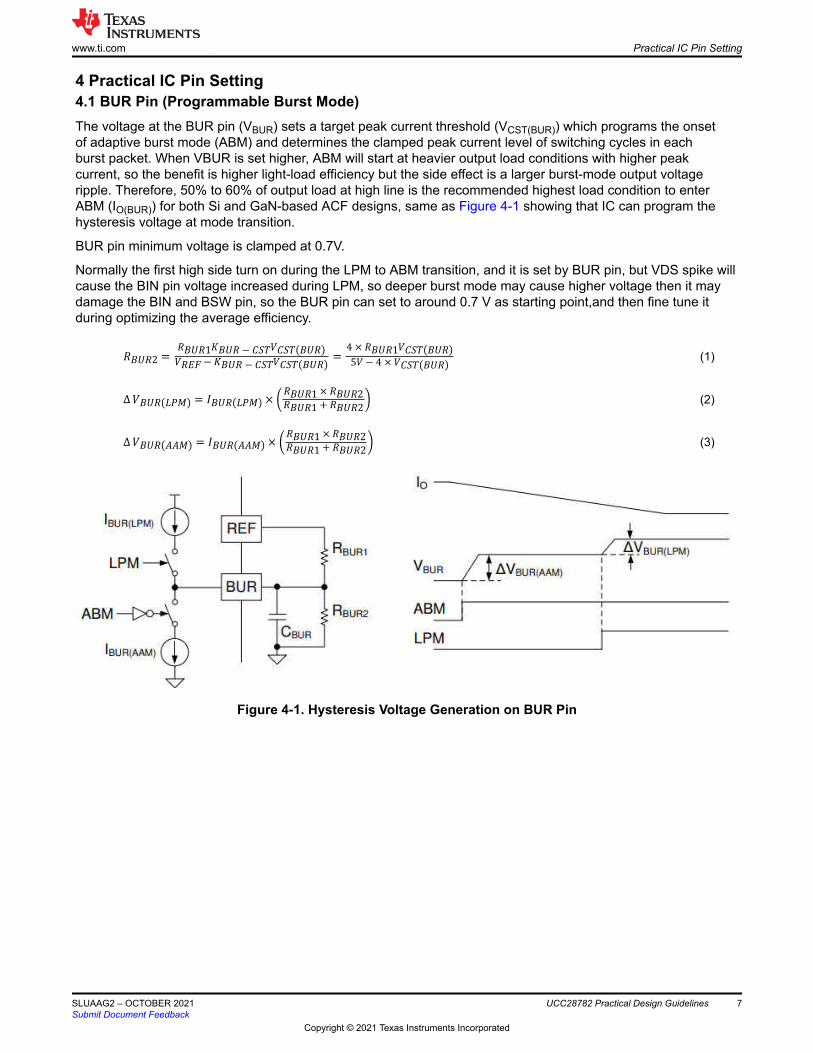
4 Practical IC Pin Setting4.1 BUR Pin (Programmable Burst Mode)The voltage at the BUR pin (VBUR) sets a target peak current threshold (VCST(BUR)) which programs the onset of adaptive burst mode (ABM) and determines the clamped peak current level of switching cycles in each burst packet. When VBUR is set higher, ABM will start at heavier output load conditions with higher peak current, so the benefit is higher light-load efficiency but the side effect is a larger burst-mode output voltage ripple. Therefore, 50% to 60% of output load at high line is the recommended highest load condition to enter ABM (IO(BUR)) for both Si and GaN-based ACF designs, same as Figure 4-1 showing that IC can program the hysteresis voltage at mode transition.
BUR pin minimum voltage is clamped at 0.7V.
Normally the first high side turn on during the LPM to ABM transition, and it is set by BUR pin, but VDS spike will cause the BIN pin voltage increased during LPM, so deeper burst mode may cause higher voltage then it may damage the BIN and BSW pin, so the BUR pin can set to around 0.7 V as starting point,and then fine tune it during optimizing the average efficiency.
RBUR2 = RBUR1KBUR − CSTVCST BURVREF − KBUR − CSTVCST BUR = 4 × RBUR1VCST BUR5V − 4 × VCST BUR (1)
∆VBUR LPM = IBUR LPM × RBUR1 × RBUR2RBUR1 + RBUR2 (2)
∆VBUR AAM = IBUR AAM × RBUR1 × RBUR2RBUR1 + RBUR2 (3)
Figure 4-1. Hysteresis Voltage Generation on BUR Pin
www.ti.com Practical IC Pin Setting
SLUAAG2 – OCTOBER 2021Submit Document Feedback
UCC28782 Practical Design Guidelines 7
Copyright © 2021 Texas Instruments Incorporated
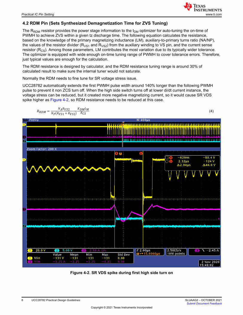
4.2 RDM Pin (Sets Synthesized Demagnetization Time for ZVS Tuning)The RRDM resistor provides the power stage information to the tDM optimizer for auto-tuning the on-time of PWMH to achieve ZVS within a given tz discharge time. The following equation calculates the resistance, based on the knowledge of the primary magnetizing inductance (LM), auxiliary-to-primary turns ratio (NA/NP), the values of the resistor divider (RVS1 and RVS2) from the auxiliary winding to VS pin, and the current sense resistor (RCS). Among those parameters, LM contributes the most variation due to its typically wider tolerance. The optimizer is equipped with wide enough on-time tuning range of PWMH to cover tolerance errors. Therefore, just typical values are enough for the calculation.
The RDM resistance is designed by calculator, and the RDM resistance tuning range is around 30% of calculated result to make sure the internal tuner would not saturate.
Normally the RDM needs to fine tune for SR voltage stress issue.
UCC28782 automatically extends the first PWMH pulse width around 140% longer than the following PWMH pulse to prevent it non ZCS turn off. When the high side switch turns off at lower di/dt current instance, the voltage stress can be reduced, but it created more negative magnetizing current, so it would cause SR VDS spike higher as Figure 4-2, so RDM resistance needs to be reduced at this case.
RRDM = NARVS2NP RVS1 + RVS2 KDMLMRCS (4)
Figure 4-2. SR VDS spike during first high side turn on
Practical IC Pin Setting www.ti.com
8 UCC28782 Practical Design Guidelines SLUAAG2 – OCTOBER 2021Submit Document Feedback
Copyright © 2021 Texas Instruments Incorporated

4.3 RTZ Pin (Sets Delay for Transition Time to Zero)The dead-time between PWMH falling edge and PWML rising edge (tz) serves as the wait time for VSW transition from its high level down to the target ZVS point. Since the optimal tZ varies with VBULK, the internal dead-time optimizer automatically extends tz as VBULK is less than the highest voltage of the input bulk capacitor (VBULK(MAX)). The circulating energy for ZVS can be further reduced, obtaining higher efficiency at low line versus a fixed dead-time over a wide line voltage range. A resistor on the RTZ pin (RRTZ) programs the minimum tZ (tZ(MIN)) at VBULK(MAX), which is the sum of the propagation delay of the high-side driver (tD(DR)) and the minimum resonant transition time of VSW falling edge (tLC(MIN)).
Normally the RTZ is designed as calculator result. If the VDS voltage has ring back voltage as Figure 4-3 showing, you need to reduce the RTZ resistance.RRTZ = KTZ × tZ MIN = KTZ × tD DR + tLC MIN (5)
tLC MIN = π− COS−1 NPS VO+ VFVBULK MAX × LMCSW (6)
Figure 4-3. RTZ Setting for the Falling-edge Transition of VSW
www.ti.com Practical IC Pin Setting
SLUAAG2 – OCTOBER 2021Submit Document Feedback
UCC28782 Practical Design Guidelines 9
Copyright © 2021 Texas Instruments Incorporated

Figure 4-4. RTZ Setting too large cause VDS ring back
Practical IC Pin Setting www.ti.com
10 UCC28782 Practical Design Guidelines SLUAAG2 – OCTOBER 2021Submit Document Feedback
Copyright © 2021 Texas Instruments Incorporated
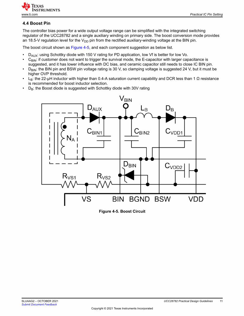
4.4 Boost PinThe controller bias power for a wide output voltage range can be simplified with the integrated switching regulator of the UCC28782 and a single auxiliary winding on primary side. The boost conversion mode provides an 18.5-V regulation level for the VDD pin from the rectified auxiliary-winding voltage at the BIN pin.
The boost circuit shown as Figure 4-5, and each component suggestion as below list.
• DAUX: using Schottky diode with 150 V rating for PD application, low Vf is better for low Vo.• CBIN: if customer does not want to trigger the survival mode, the E-capacitor with larger capacitance is
suggested, and it has lower influence with DC bias, and ceramic capacitor still needs to close IC BIN pin.• DBIN: the BIN pin and BSW pin voltage rating is 30 V, so clamping voltage is suggested 24 V, but it must be
higher OVP threshold.• LB: the 22-μH inductor with higher than 0.4-A saturation current capability and DCR less than 1 Ω resistance
is recommended for boost inductor selection.• DB: the Boost diode is suggested with Schottky diode with 30V rating
Figure 4-5. Boost Circuit
www.ti.com Practical IC Pin Setting
SLUAAG2 – OCTOBER 2021Submit Document Feedback
UCC28782 Practical Design Guidelines 11
Copyright © 2021 Texas Instruments Incorporated
5 Transformer designACF is designed for high switching frequency application, so there are several item also need to be careful during the transformer design, and these suggestion is based on 60W PD design.
Using Litz wire for bobbin design
The ACF is designed for high switching frequency application, and its switching frequency may up to 500KHz during the ABM, so the skin effect will cause lots of ACR loss, the suggested primary side winding is 20*0.05mm, and secondary side winding is 150*0.05mm. Aux-winding DCR need to less than 0.1Ω.
Core material
Same as previous mention that switching may up to 500KHz, so Core material suggest optimized with 300KHz~500KHz range to reduce the core loss, and there are some suggested core material as below list. The Bmax also suggest to within 0.2T to reduce the core loss.
TDK-N49; Ferroxcube-3F36; Hitachi-ML90S
Turn ratio
The turn ratio is limited by primary side MOS and SR MOS voltage rating, turn ratio within 5~6 is suggested for 20V PD application.
Maximum turn ratio (NPS(MAX)) is limited by the maximum derated drain-to-source voltage of low side MOS (VDS_QL(MAX)). In the expression below, ∆VCLAMP is a voltage deviation above the reflected output voltage. It can be either the ripple voltage of CCLAMP in AAM mode, or the voltage over-charge of CCLAMP by the leakage inductance energy when high side MOS is disabled in LPM. VO is the output voltage, and VF is the forward voltage drop of the secondary rectifier.
NPS MAX = VDS_QL MAX − VBULK MAX − ∆VCLAMPVO+ VF (7)
Minimum turn ratio (NPS(MIN)) is limited by the maximum derated drain-to-source voltage of the secondary rectifier (VDS_SR(MAX)). In the expression for NPS(MIN), ∆VSPIKE should account for any additional voltage spike higher than VBULK(MAX)/NPS that occurs when high side MOS is active and turns-off at non-zero current in AAM mode.
NPS MIN = VBULK MAXVDS_SR MAX − VO − ∆VSPIKE (8)
Inductance
Lm can be estimated based on minimum switching frequency (FSW(MIN)) at VBULK(MIN), maximum duty cycle (DMAX), and output power at highest nominal output voltage, nominal full-load current (PO(FL)).
Lr is suggested within 3uH to reduce the VDS spike during LPM.
DMAX = NPS VO+ VFVBULK MIN + NPS VO+ VF (9)
LM = DMAX2 VBULK MIN2 η2PO FL × 1− KRESFSW MIN (10)
Transformer design www.ti.com
12 UCC28782 Practical Design Guidelines SLUAAG2 – OCTOBER 2021Submit Document Feedback
Copyright © 2021 Texas Instruments Incorporated
6 References1. Texas Instruments, UCC28782 High-Density Active-Clamp Flyback Controller with EMI Dithering, X-
CapDischarge, and Bias Power Management data sheet.2. Texas Instruments, UCC28782 design calculator tool.3. Texas Instruments, 65W ACF for PD application user guide.4. Texas Instruments, 65W ZVS flyback for PD application reference guide.5. Texas Instruments, 100W PFC + ACF with Si-MOS application reference guide.6. Texas Instruments, 100W PFC + ACF with GaN application reference guide.7. Texas Instruments, Transformer structures that achieve low EMI with low and high side rectifiers publication.8. Texas Instruments, Flyback Transformer Design for Efficiency and EMI9. Texas Instruments, Designing Low EMI Power Converters for Industrial and Automotive Systems
presentation.10. Texas Instruments, Input EMI Filter Design for Offline Phase-Dimmable LED Power Supplies presentation.
www.ti.com References
SLUAAG2 – OCTOBER 2021Submit Document Feedback
UCC28782 Practical Design Guidelines 13
Copyright © 2021 Texas Instruments Incorporated

IMPORTANT NOTICE AND DISCLAIMERTI PROVIDES TECHNICAL AND RELIABILITY DATA (INCLUDING DATA SHEETS), DESIGN RESOURCES (INCLUDING REFERENCE DESIGNS), APPLICATION OR OTHER DESIGN ADVICE, WEB TOOLS, SAFETY INFORMATION, AND OTHER RESOURCES “AS IS” AND WITH ALL FAULTS, AND DISCLAIMS ALL WARRANTIES, EXPRESS AND IMPLIED, INCLUDING WITHOUT LIMITATION ANY IMPLIED WARRANTIES OF MERCHANTABILITY, FITNESS FOR A PARTICULAR PURPOSE OR NON-INFRINGEMENT OF THIRD PARTY INTELLECTUAL PROPERTY RIGHTS.These resources are intended for skilled developers designing with TI products. You are solely responsible for (1) selecting the appropriate TI products for your application, (2) designing, validating and testing your application, and (3) ensuring your application meets applicable standards, and any other safety, security, regulatory or other requirements.These resources are subject to change without notice. TI grants you permission to use these resources only for development of an application that uses the TI products described in the resource. Other reproduction and display of these resources is prohibited. No license is granted to any other TI intellectual property right or to any third party intellectual property right. TI disclaims responsibility for, and you will fully indemnify TI and its representatives against, any claims, damages, costs, losses, and liabilities arising out of your use of these resources.TI’s products are provided subject to TI’s Terms of Sale or other applicable terms available either on ti.com or provided in conjunction with such TI products. TI’s provision of these resources does not expand or otherwise alter TI’s applicable warranties or warranty disclaimers for TI products.TI objects to and rejects any additional or different terms you may have proposed. IMPORTANT NOTICE
Mailing Address: Texas Instruments, Post Office Box 655303, Dallas, Texas 75265Copyright © 2021, Texas Instruments Incorporated