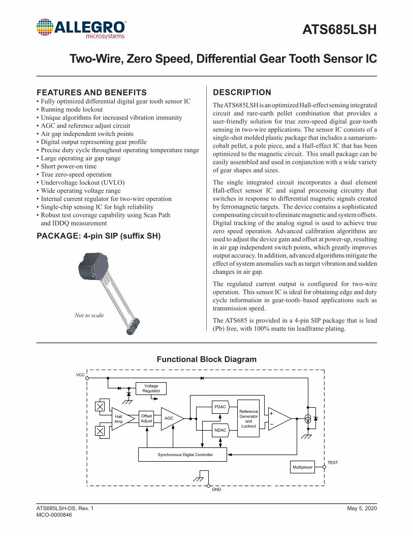
Two-Wire, Zero Speed Differential Gear Tooth Sensor IC
15
FEATURES AND BENEFITS • Fully optimized differential digital gear tooth sensor IC • Running mode lockout • Unique algorithms for increased vibration immunity • AGC and reference adjust circuit • Air gap independent switch points • Digital output representing gear profile • Precise duty cycle throughout operating temperature range • Large operating air gap range • Short power-on time • True zero-speed operation • Undervoltage lockout (UVLO) • Wide operating voltage range • Internal current regulator for two-wire operation • Single-chip sensing IC for high reliability • Robust test coverage capability using Scan Path and IDDQ measurement DESCRIPTION The ATS685LSH is an optimized Hall-effect sensing integrated circuit and rare-earth pellet combination that provides a user-friendly solution for true zero-speed digital gear-tooth sensing in two-wire applications. The sensor IC consists of a single-shot molded plastic package that includes a samarium- cobalt pellet, a pole piece, and a Hall-effect IC that has been optimized to the magnetic circuit. This small package can be easily assembled and used in conjunction with a wide variety of gear shapes and sizes. The single integrated circuit incorporates a dual element Hall-effect sensor IC and signal processing circuitry that switches in response to differential magnetic signals created by ferromagnetic targets. The device contains a sophisticated compensating circuit to eliminate magnetic and system offsets. Digital tracking of the analog signal is used to achieve true zero speed operation. Advanced calibration algorithms are used to adjust the device gain and offset at power-up, resulting in air gap independent switch points, which greatly improves output accuracy. In addition, advanced algorithms mitigate the effect of system anomalies such as target vibration and sudden changes in air gap. The regulated current output is configured for two-wire operation. This sensor IC is ideal for obtaining edge and duty cycle information in gear-tooth–based applications such as transmission speed. The ATS685 is provided in a 4-pin SIP package that is lead (Pb) free, with 100% matte tin leadframe plating. ATS685LSH-DS, Rev. 1 MCO-0000846 Two-Wire, Zero Speed, Differential Gear Tooth Sensor IC PACKAGE: 4-pin SIP (suffix SH) Functional Block Diagram Not to scale ATS685LSH GND VCC TEST Multiplexor Voltage Regulator Hall Amp Offset Adjust Reference Generator and Lockout PDAC AGC Synchronous Digital Controller NDAC May 5, 2020
Transcript of Two-Wire, Zero Speed Differential Gear Tooth Sensor IC
FEATURES AND BENEFITS• Fully optimized differential digital gear tooth sensor IC• Running mode lockout• Unique algorithms for increased vibration immunity• AGC and reference adjust circuit• Air gap independent switch points• Digital output representing gear profile• Precise duty cycle throughout operating temperature range• Large operating air gap range• Short power-on time• True zero-speed operation• Undervoltage lockout (UVLO)• Wide operating voltage range• Internal current regulator for two-wire operation• Single-chip sensing IC for high reliability• Robust test coverage capability using Scan Path
and IDDQ measurement
DESCRIPTIONThe ATS685LSH is an optimized Hall-effect sensing integrated circuit and rare-earth pellet combination that provides a user-friendly solution for true zero-speed digital gear-tooth sensing in two-wire applications. The sensor IC consists of a single-shot molded plastic package that includes a samarium-cobalt pellet, a pole piece, and a Hall-effect IC that has been optimized to the magnetic circuit. This small package can be easily assembled and used in conjunction with a wide variety of gear shapes and sizes.
The single integrated circuit incorporates a dual element Hall-effect sensor IC and signal processing circuitry that switches in response to differential magnetic signals created by ferromagnetic targets. The device contains a sophisticated compensating circuit to eliminate magnetic and system offsets. Digital tracking of the analog signal is used to achieve true zero speed operation. Advanced calibration algorithms are used to adjust the device gain and offset at power-up, resulting in air gap independent switch points, which greatly improves output accuracy. In addition, advanced algorithms mitigate the effect of system anomalies such as target vibration and sudden changes in air gap.
The regulated current output is configured for two-wire operation. This sensor IC is ideal for obtaining edge and duty cycle information in gear-tooth–based applications such as transmission speed.
The ATS685 is provided in a 4-pin SIP package that is lead (Pb) free, with 100% matte tin leadframe plating.
ATS685LSH-DS, Rev. 1MCO-0000846
Two-Wire, Zero Speed, Differential Gear Tooth Sensor IC
PACKAGE: 4-pin SIP (suffix SH)
Functional Block Diagram
Not to scale
ATS685LSH
GND
VCC
TESTMultiplexor
VoltageRegulator
HallAmp
OffsetAdjust
ReferenceGenerator
andLockout
PDAC
AGC
Synchronous Digital Controller
NDAC
May 5, 2020

Two-Wire, Zero Speed, Differential Gear Tooth Sensor IC ATS685LSH
2Allegro MicroSystems 955 Perimeter Road Manchester, NH 03103-3353 U.S.A.www.allegromicro.com
Pinout Diagram Terminal List TableNumber Name Function
1 VCC Supply voltage
2 NC No connection (float or tie to GND)
3 TEST Test (float or tie to GND)
4 GND Ground
Selection GuidePart Number Packing*
ATS685LSHTN-T 13-in. reel, 800 pieces per reel*Contact Allegro™ for additional packing options
Absolute Maximum RatingsCharacteristic Symbol Notes Rating Units
Supply Voltage VCC 26.5 V
Reverse Supply Voltage VRCC –18 V
Operating Ambient Temperature TA Range L, refer to Power Derating Curve –40 to 150 ºC
Maximum Junction Temperature TJ(max) 165 ºC
Storage Temperature Tstg –65 to 170 ºC
2 431

Two-Wire, Zero Speed, Differential Gear Tooth Sensor IC ATS685LSH
3Allegro MicroSystems 955 Perimeter Road Manchester, NH 03103-3353 U.S.A.www.allegromicro.com
OPERATING CHARACTERISTICS VCC and TA within specification, unless otherwise notedCharacteristics Symbol Test Conditions Min. Typ.1 Max. Unit2
Electrical CharacteristicsSupply Voltage3 VCC Operating, TJ < TJ (max), ICC within specification 4.0 – 24 V
Undervoltage Lockout VCC(UV) VCC 0 → 5 V or 5 → 0 V – 3.5 3.95 V
Reverse Supply Current4 IRCC VCC = –18 V – – –10 mA
Supply Zener Clamp Voltage VZ ICC = ICC (max) + 3 mA, TA = 25°C 28 – – V
Supply Zener Current IZ TA = 25°C, VCC = 28 V – – 19 mA
Supply CurrentICC(Low) Low-current state 4 6 8 mA
ICC(High) High-current state 12 14 16 mA
Supply Current Ratio ICC(High) / ICC(Low)
Ratio of high current to low current 1.85 – 3.05 –
Test Pin Zener Clamp Voltage5 VZTEST – 6 – V
Power-On State CharacteristicsPower-On Time6 tPO VCC > VCC (min), fOP < 100 Hz – 1 2 ms
Power-On State7 POS t > tPO – ICC(High) – A
Output Stage
Output Slew Rate8,9 di / dt Δi / Δt from 90% to 10% ICC level RSENSE = 100 Ω, CLOAD = 10 pF, no CBYPASS
7 14 – mA/μs
Performance CharacteristicsOperating Frequency fOP 0 – 12 kHz
Analog Signal Bandwidth BW 16 20 – kHz
Operate Point BOP% of peak-to-peak BSIG , AGOP within specification – 70 – %
Release Point BRP% of peak-to-peak BSIG , AGOP within specification – 30 – %
Running Mode Lockout Enable Threshold VLOE(RM)
At peak-to-peak VPROC < VLOE(RM) , output switching disables – 170 – mV
Running Mode Lockout Release Threshold VLOR(RM)
At peak-to-peak VPROC > VLOR(RM) , output switching enables – 200 – mV
CalibrationStart Mode Hysteresis POHYS – VLOR(RM) – mV
Initial Calibration10 CALI Rising output (current) edges, fOP < 200 Hz – – 3 edges
Continued on the next page…

Two-Wire, Zero Speed, Differential Gear Tooth Sensor IC ATS685LSH
4Allegro MicroSystems 955 Perimeter Road Manchester, NH 03103-3353 U.S.A.www.allegromicro.com
Functional Characteristics
Operating Signal Range11 BSIGDifferential magnetic signal, duty cycle within specification 50 – 1500 GPK-PK
Extended Operating Signal Range BSIGEXTDifferential magnetic signal, output switching (no missed edges), duty cycle not guaranteed 30 – – GPK-PK
Operational Air Gap Range AGOPUsing Allegro Reference Target 60-0, duty cycle within specification 0.5 – 2.5 mm
Extended Operational Air Gap Range AGEXT
Using Allegro Reference Target 60-0, output switching (no missed edges), duty cycle not guaranteed
– – 3.0 mm
Allowable User-Induced Differential Offset BDIFFEXT Operation within specification ±60 – – G
Duty Cycle Variation12 ΔD Wobble < 0.5 mm, AG within specification – – ±10 %
Maximum Sudden Signal Amplitude Change BSIG(INST)
Instantaneous symmetric magnetic signal amplitude change, measured as a percentage of peak-to-peak BSIG, fOP < 500 Hz
– 45 – %
1Typical values are at TA = 25°C and VCC = 12 V. Performance may vary for individual units, within the specified maximum and minimum limits.21 G (gauss) = 0.1 mT (millitesla).3Maximum voltage must be adjusted for power dissipation and junction temperature; see Power Derating section.4Negative current is defined as conventional current coming out of (sourced from) the specified device terminal.5Sustained voltages beyond the clamp voltage may cause permanent damage to the IC.6Measured from VCC ≥ VCC (min) to the time when the device is able to switch the output signal in response to a magnetic stimulus.7Please refer to the Functional Description, Power-On section.8di is the difference between 10% of ICC(Low) and 90% of ICC(High) . dt is the time period between those two points.9CLOAD is the probe capacitance of the oscilloscope used to make the measurement.10For power-on frequency, fOP < 200 Hz. Higher power-on frequencies may result in more input magnetic cycles until full output edge accuracy is achieved, including the possibility of missed output edges.11AGOP is dependent on the available magnetic field. The available field is dependent on target geometry and material and should be independently characterized. The field available from the reference target is given in the Reference Target table.12Target rotation from pin 4 to pin 1.
OPERATING CHARACTERISTICS (continued) VCC and TA within specification, unless otherwise notedCharacteristics Symbol Test Conditions Min. Typ.1 Max. Unit2

Two-Wire, Zero Speed, Differential Gear Tooth Sensor IC ATS685LSH
5Allegro MicroSystems 955 Perimeter Road Manchester, NH 03103-3353 U.S.A.www.allegromicro.com
Reference Gear Magnetic ProfileReference Target 60-0, Hall element spacing 2.20 mm
Gear Rotation (°)
Air Gap (mm)
Diff
eren
tial B
(G)
0 2 4 6 8 10 12 14 16 18 20600
400
200
0
200
400
600
0.50 mm AG
3.00 mm AG
0.50
0.75
1.00
1.25
1.50
1.75
2.00
2.25
2.50
2.75
3.00
1 20 3
1200
1000
800
600
400
200
0
Reference Gear Magnetic Gradient Amplitude versus Air GapReference Target 60-0, Hall element spacing 2.20 mm
Air Gap (mm)
Peak
-to-P
eak
Diff
eren
tial B
(G)
Reference Target 60-0 (60 Tooth Target)
Characteristics Symbol Test Conditions Typ. Units Symbol Key
Outside Diameter Do Outside diameter of target 120 mm
tt V
ØDOht
FBranded Faceof Package
Air Gap
Face Width FBreadth of tooth, with respect to branded face
6 mm
Angular Tooth Thickness tLength of tooth, with respect to branded face
3 deg.
Angular Valley Thickness tvLength of valley, with respect to branded face
3 deg.
Tooth Whole Depth ht 3 mm
Material Low Carbon Steel – –
Reference Target60-0
of PackageBranded Face
Two-Wire, Zero Speed, Differential Gear Tooth Sensor IC ATS685LSH
6Allegro MicroSystems 955 Perimeter Road Manchester, NH 03103-3353 U.S.A.www.allegromicro.com
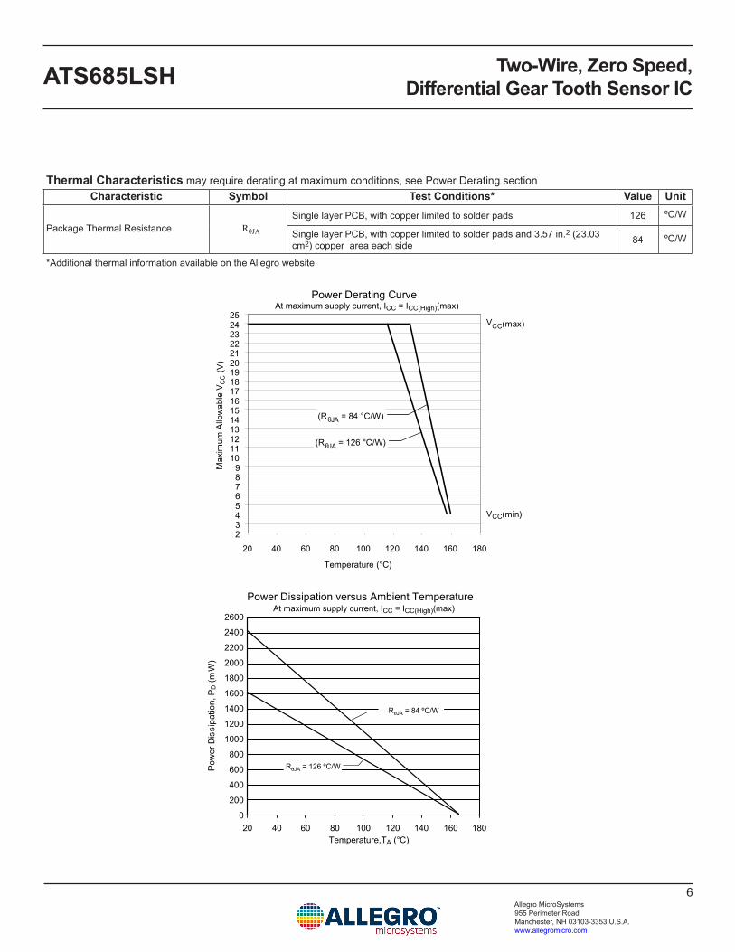
Thermal Characteristics may require derating at maximum conditions, see Power Derating sectionCharacteristic Symbol Test Conditions* Value Unit
Package Thermal Resistance RθJA
Single layer PCB, with copper limited to solder pads 126 ºC/W
Single layer PCB, with copper limited to solder pads and 3.57 in.2 (23.03 cm2) copper area each side 84 ºC/W
*Additional thermal information available on the Allegro website
23456789
10111213141516171819202122232425
Temperature (°C)
Max
imum
Allo
wab
le V
CC
(V)
VCC(max)
VCC(min)
Power Derating CurveAt maximum supply current, ICC = ICC(High)(max)
20 40 60 80 100 120 140 160 180
(RθJA = 84 °C/W)
(RθJA = 126 °C/W)
2600
2400
2200
2000
1800
1600
1400
1200
1000
800
600
400
200
020 40 60 80 100 120 140 160 180
Temperature,TA (°C)
Pow
er D
issi
patio
n, P
D (m
W)
RθJA = 126 ºC/W
RθJA = 84 ºC/W
Power Dissipation versus Ambient TemperatureAt maximum supply current, ICC = ICC(High)(max)

Two-Wire, Zero Speed, Differential Gear Tooth Sensor IC ATS685LSH
7Allegro MicroSystems 955 Perimeter Road Manchester, NH 03103-3353 U.S.A.www.allegromicro.com
Functional Description
Sensing TechnologyThe ATS685 sensor IC contains a single-chip differential Hall-effect circuit, a samarium cobalt pellet, and a flat ferrous pole piece (a precisely mounted magnetic field concentrator that homogenizes the flux passing through the Hall chip). As shown in figure 1, the circuit supports two Hall elements, which sense the
magnetic profile of the ferromagnetic gear target simultaneously, but at different points (spaced at a 2.2 mm pitch), generating a differential internal analog voltage, VPROC , that is processed for precise switching of the digital output signal.
The Hall IC is self-calibrating and integrates a temperature compensated amplifier and offset cancellation circuitry. Its volt-age regulator provides supply noise rejection throughout the operating voltage range. Changes in temperature do not greatly affect this device due to the stable amplifier design and the offset rejection circuitry. The Hall transducers and signal processing electronics are integrated on the same silicon substrate, using a proprietary BiCMOS process.
Target Profiling During OperationUnder normal operating conditions, the IC is capable of provid-ing digital information that is representative of the mechanical features of a rotating gear. The waveform diagram in figure 2 presents the automatic translation of the mechanical profile, through the magnetic profile that it induces, to the digital output signal of the ATS685. No additional optimization is needed and minimal processing circuitry is required. This ease of use reduces design time and incremental assembly costs for most applications.
DiagnosticsThe regulated current output is configured for two-wire applica-tions, requiring one less wire for operation than do switches with the traditional open-collector output. Additionally, the system designer inherently gains diagnostics because there is always output current flowing, which should be in either of two nar-row ranges, shown in figure 3 as ICC(HIGH) and ICC(LOW). Any current level not within these ranges indicates a fault condition. If ICC > ICC(HIGH)(max), then a short condition exists, and if ICC < ICC(LOW)(min), then an open condition exists. Any value of ICC between the allowed ranges for ICC(HIGH) and ICC(LOW) indicates a general fault condition.
Target (Gear)
Back-biasingRare-earth Pellet
South Pole
North Pole Case
(Pin 1 Side)(Pin 4 Side)
Hall ICPole Piece
Element Pitch
(Concentrator)Dual-Element
Hall Effect Device
Hall Element 1Hall Element 2
Figure 1. Relative motion of the target is detected by the dual Hall elements mounted on the Hall IC.
Figure 2. The magnetic profile reflects the geometry of the target, allowing the ATS685 to present an accurate digital output response.
BOP(#1)
BRP(#1)
BOP(#2)
Off OnOnOffDevice Internal Switch State
Device Package Orientation to Target
Device Internal Differential Analog Signal, VPROC
Device Output Signal, ICC
(Pin 1 Side)(Pin 4 Side) IC
Element Pitch
Hall Element 1Hall Element 2Device Branded Face
Target Magnetic Profile+B
+t
+t
Mechanical Position (Target moves past sensor pin 1 to pin 4)
Target(Gear)
This tooth sensed earlier
This tooth sensed later
(View of Side Away from Pins)
ICC(HIGH)(max)
ICC(HIGH)(min)
ICC(LOW)(max)
ICC(LOW)(min)
Range for Valid ICC(HIGH)
Range for Valid ICC(LOW)
0
+mA
Short
Fault
Open
Figure 3. Diagnostic characteristics of supply current values.

Two-Wire, Zero Speed, Differential Gear Tooth Sensor IC ATS685LSH
8Allegro MicroSystems 955 Perimeter Road Manchester, NH 03103-3353 U.S.A.www.allegromicro.com
Determining Output Signal PolarityIn figure 2, the top panel, labeled Mechanical Position, represents the mechanical features of the target gear and orientation to the device. The bottom panel, labeled Device Output Signal, displays the square waveform corresponding to the digital output signal (current amplitude) that results from a rotating gear configured as shown in figure 3. Referring to the target side nearest the face of the sensor IC, the direction of rotation is: perpendicular to the leads, across the face of the device, from the pin 1 side to the pin 4 side.
In order to read the output signal as a voltage, VSENSE , a sense resistor, RSENSE , can be placed on either the VCC signal or on the GND signal. As shown in figure 4, when RSENSE is placed on the GND signal, the output signal voltage, VSENSE(LowSide) , is in phase with ICC . When RSENSE is placed on the VCC signal, the output signal voltage, VSENSE(HighSide) , is inverted relative to ICC .
Rotating TargetBrandeof Package
Pin 1 Pin 4
d Face
Figure 3. This figure depicts left-to-right (pin 1 to pin 4) direction of target rotation.
Figure 4. Alternative Polarity Configurations Using Two-Wire Sensing. The Output Polarity States table provides the permutations of output voltage relative to ICC, given alternative locations for RSENSE. Panel A shows the low-side, VSENSE(LowSide) , sensing configuration, and panel B shows the high-side, VSENSE(HighSide) , configuration. As shown in panel C, VSENSE(LowSide) is in phase with ICC , and VSENSE(HighSide) , is inverted.
ATS685
VCC
GND
VCC
1
4
ATS685
VCC
GND
VCC
1
4
VSENSE(HighSide)
VSENSE(LowSide)
RSENSE
RSENSE
ICC ICC
Output Polarity StatesRSENSE Location ICC State VSENSE State
High side(VCC pin side)
High Low
Low High
Low side(GND pin side)
High High
Low Low
ICC
VSENSE(HighSide)
V+
VSENSE(LowSide)
V+
I+

Two-Wire, Zero Speed, Differential Gear Tooth Sensor IC ATS685LSH
9Allegro MicroSystems 955 Perimeter Road Manchester, NH 03103-3353 U.S.A.www.allegromicro.com
(A) TEAG varying; cases such as eccentric mount, out-of-round region, normal operation position shift
(B) Internal analog signal, VPROC, typically resulting in the IC
0
BOP
BRP
BOP
BRP
BOP
BRP
BOP
BRP
BOP
BOP
BRP
360Target Rotation (°)
Hysteresis Band(Delimited by switchpoints)
VP
RO
C (V
)V+
(C) Internal analog signal, VPROC, representing magnetic field for digital output
VP
RO
C (V
)V
OU
T (V
)
V+
LargerTEAG
SmallerTEAGIC
Target
LargerTEAG
Target
IC
SmallerTEAG
SmallerTEAG
Figure 5. The Continuous Update algorithm allows the Allegro IC to interpret and adapt to variances in the magnetic field generated by the target as a result of eccentric mounting of the target, out-of-round target shape, and similar dynamic application problems that affect the TEAG (Total Effective Air Gap). As shown in panel A, the variance in the target position results in a change in the TEAG. This affects the IC as a varying magnetic field, which results in proportional changes in the internal analog signal, VPROC, shown in panel B. The Continuous Update algorithm is used to establish switch points based on the fluctuation of VPROC, as shown in panel C.
Continuous Update of Switch Points Switch points are the threshold levels of the differential internal analog signal, VPROC , at which the device changes output signal state. The value of VPROC is directly proportional to the magnetic flux density, B, induced by the target and sensed by the Hall elements. As VPROC rises through a certain limit, referred to as the operate point, BOP , the output state changes from high to low. As VPROC falls below BOP to a certain limit, the release point, BRP , the output state changes from low to high.
As shown in figure 5, threshold levels for the switch points are established as a function of the peak input signal levels. The device incorporates an algorithm that continuously monitors the input signal and updates the switching thresholds accordingly with limited inward movement of VPROC. The switch point for each edge is determined by the detection of the previous two signal edges. In this manner, variations are tracked in real time.

Two-Wire, Zero Speed, Differential Gear Tooth Sensor IC ATS685LSH
10Allegro MicroSystems 955 Perimeter Road Manchester, NH 03103-3353 U.S.A.www.allegromicro.com
Power-OnThe ATS685 is guaranteed to power-on in the high current state, ICC(High) . When power (VCC > VCC (min) ) is applied to the device, a short period of time is required to power the vari-ous portions of the circuit. During this period, the ATS685 will power-on in the high current state, ICC(High) .
Initial Edge DetectionThe device self-calibrates using the initial teeth sensed, and then
enters running mode. This results in reduced accuracy for a brief period, CALI . However, this period allows the device to optimize for running mode operation. As shown in figure 6, the first three high peak signals corresponding to rising output edges are used to calibrate AGC (Automatic Gain Control). There is a slight vari-ance in the duration of initialization, depending on what target feature is opposite the sensor IC when power-on occurs. Also, a high speed of target rotation at power-on may increase the quan-tity required in the CALI period.
Figure 6. Power-On Initial Edge Detection. This figure demonstrates four typical power-on scenarios. All these examples assume that the target is moving relative to the sensor IC in the direction indicated (from pin 1 to pin 4) and the voltage output is configured for low-side sensing, VOUT(Low). The length of time required to overcome Start Mode Hysteresis, as well as the combined effect of whether it is overcome in a positive or negative direction plus whether the next edge is in that same or opposite polarity, affect the point in time when AGC calibration begins. Three high peaks are always required for AGC calibration when fOP ≤ 200 Hz, and more may be required at greater speeds.
Target(Gear)
ICC
V PRO
C
V PRO
C
V PRO
C
V PRO
C
V PRO
C
V PRO
C
V PRO
C
V PRO
C
ICC
ICC
ICC
ICC
ICC
ICCICC
Power-onoppositetooth
Power-onat fallingmechanicaledge
Power-onat risingmechanicaledge
Power-onoppositevalley
AGC Calibration Running Mode
AGC Calibration Running Mode
AGC Calibration Running Mode
AGC Calibration Running Mode
Device Position 1
1
4
4
2
2
3
3
Start Mode Hysteresis Overcome
Start Mode Hysteresis Overcome
Start Mode Hysteresis Overcome
Start Mode Hysteresis Overcome
Two-Wire, Zero Speed, Differential Gear Tooth Sensor IC ATS685LSH
11Allegro MicroSystems 955 Perimeter Road Manchester, NH 03103-3353 U.S.A.www.allegromicro.com
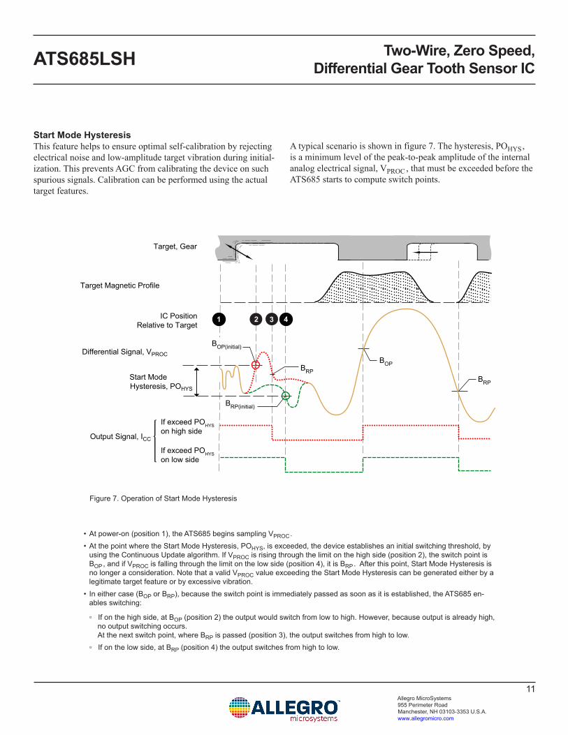
Start Mode HysteresisThis feature helps to ensure optimal self-calibration by rejecting electrical noise and low-amplitude target vibration during initial-ization. This prevents AGC from calibrating the device on such spurious signals. Calibration can be performed using the actual target features.
A typical scenario is shown in figure 7. The hysteresis, POHYS , is a minimum level of the peak-to-peak amplitude of the internal analog electrical signal, VPROC , that must be exceeded before the ATS685 starts to compute switch points.
BOP
BRP
BRP
BRP(initial)
BOP(initial)
1 42 3
Start Mode
Output Signal, ICC
If exceed POHYSon high side
If exceed POHYSon low side
IC Position Relative to Target
Target Magnetic Profile
Differential Signal, VPROC
Target, Gear
Hysteresis, POHYS
Figure 7. Operation of Start Mode Hysteresis
• At power-on (position 1), the ATS685 begins sampling VPROC .• At the point where the Start Mode Hysteresis, POHYS, is exceeded, the device establishes an initial switching threshold, by
using the Continuous Update algorithm. If VPROC is rising through the limit on the high side (position 2), the switch point is BOP , and if VPROC is falling through the limit on the low side (position 4), it is BRP . After this point, Start Mode Hysteresis is no longer a consideration. Note that a valid VPROC value exceeding the Start Mode Hysteresis can be generated either by a legitimate target feature or by excessive vibration.
• In either case (BOP or BRP), because the switch point is immediately passed as soon as it is established, the ATS685 en-ables switching:
If on the high side, at BOP (position 2) the output would switch from low to high. However, because output is already high, no output switching occurs. At the next switch point, where BRP is passed (position 3), the output switches from high to low.
If on the low side, at BRP (position 4) the output switches from high to low.

Two-Wire, Zero Speed, Differential Gear Tooth Sensor IC ATS685LSH
12Allegro MicroSystems 955 Perimeter Road Manchester, NH 03103-3353 U.S.A.www.allegromicro.com
Undervoltage LockoutWhen the supply voltage falls below the minimum operating voltage, VCC(UV) , ICC goes high and remains high regardless of the state of the magnetic gradient from the target. This lockout feature prevents false signals, caused by undervoltage conditions, from propagating to the output of the device. Because VCC is below the VCC(min) specification during lockout, the ICC levels may not be within specification.
Power Supply ProtectionThe device contains an on-chip regulator and can operate over a wide VCC range. For devices that need to operate from an unregu-lated power supply, transient protection must be added externally. For applications using a regulated line, EMI/RFI protection may still be required. Contact Allegro for information on the circuitry needed for compliance with various EMC specifications. Refer to figure 8 for an example of a basic application circuit.
Automatic Gain Control (AGC)This feature allows the device to operate with an optimal internal electrical signal, regardless of the air gap (within the AG specifica-tion). At power-on, the device determines the peak-to-peak ampli-tude of the signal generated by the target. The gain is then auto-matically adjusted. Figure 9 illustrates the effect of this feature.
Running Mode Gain AdjustThe ATS685 has a feature during Running mode to compensate for dynamic air gap variation. If the system increases the mag-
netic input drastically, the device will gradually readjust the gain downwards, allowing the chip to regain the optimum internal electrical signal with the new, larger, magnetic signal.
Dynamic Offset Cancellation (DOC)The offset circuitry when combined with AGC automatically reduces the effects of chip, magnet, and installation offsets. This circuitry is continuously active, including both Power-on mode and Running mode, compensating for any offset drift (within Allowable User-Induced Differential Offset). Continuous opera-tion also allows it to compensate for offsets induced by tempera-ture variations over time.
Running Mode LockoutThe ATS685 has a Running mode lockout feature to prevent switching on small signals that are characteristic of vibration signals. The internal logic of the chip evaluates small signal amplitudes below a certain level to be vibration. In that event, the output is blanked (locked-out) until the amplitude of the signal returns to normal operating levels.
WatchdogThe ATS685 employs a watchdog circuit to prevent extended loss of output switching during sudden impulses and vibration in the system. If the system changes the magnetic input drastically such that target feature detection is terminated, the device will fully reset itself, allowing the chip to recalibrate properly on the new magnetic input signal.
Mechanical Profile
AGSmall
AGLarge
AGSmallAGLarge
Internal DifferentialAnalog Signal
Response, with AGC
Internal DifferentialAnalog Signal
Response, without AGC
Ferrous Target
V+
V+
Figure 9. Automatic Gain Control (AGC). The AGC function corrects for variances in the air gap. Differences in the air gap cause differences in the magnetic field at the device, but AGC prevents that from affecting device performance, as shown in the lowest panel.
Figure 8. Typical circuit for proper device operation.
2 ATS685
1
3
4
0.01 µF (optional)
100 ΩRSENSE CLOAD
CBYPASS
VCC

Two-Wire, Zero Speed, Differential Gear Tooth Sensor IC ATS685LSH
13Allegro MicroSystems 955 Perimeter Road Manchester, NH 03103-3353 U.S.A.www.allegromicro.com
Power Derating
The device must be operated below the maximum junction temperature of the device, TJ(max). Under certain combinations of peak conditions, reliable operation may require derating supplied power or improving the heat dissipation properties of the appli-cation. This section presents a procedure for correlating factors affecting operating TJ. (Thermal data is also available on the Allegro website.)
The Package Thermal Resistance, RθJA, is a figure of merit sum-marizing the ability of the application and the device to dissipate heat from the junction (die), through all paths to the ambient air. Its primary component is the Effective Thermal Conductivity, K, of the printed circuit board, including adjacent devices and traces. Radiation from the die through the device case, RθJC, is relatively small component of RθJA. Ambient air temperature, TA, and air motion are significant external factors, damped by overmolding.
The effect of varying power levels (Power Dissipation, PD), can be estimated. The following formulas represent the fundamental relationships used to estimate TJ, at PD.
PD = VIN × IIN (1)
ΔT = PD × RθJA (2)
TJ = TA + ΔT (3)
For example, given common conditions such as: TA= 25°C, VCC = 12 V, ICC = 6 mA, and RθJA = 126 °C/W, then:
PD = VCC × ICC = 12 V × 6 mA = 72 mW
ΔT = PD × RθJA = 72 mW × 126 °C/W = 9.1°C
TJ = TA + ΔT = 25°C + 9.1°C = 34.1°CA worst-case estimate, PD(max), represents the maximum allow-able power level (VCC(max), ICC(max)), without exceeding TJ(max), at a selected RθJA and TA.
Example: Reliability for VCC at TA = 150°C, package SH, using a single-layer PCB.
Observe the worst-case ratings for the device, specifically: RθJA = 126 °C/W, TJ(max) = 165°C, VCC(max) = 28 V, and ICC(max) = 16 mA.
Calculate the maximum allowable power level, PD(max). First, invert equation 3:
ΔTmax = TJ(max) – TA = 165 °C – 150 °C = 15 °C
This provides the allowable increase to TJ resulting from internal power dissipation. Then, invert equation 2:
PD(max) = ΔTmax ÷ RθJA = 15°C ÷ 126 °C/W = 119 mWFinally, invert equation 1 with respect to voltage:
VCC(est) = PD(max) ÷ ICC(max) = 119 mW ÷ 16 mA = 7.4 VThe result indicates that, at TA, the application and device can dissipate adequate amounts of heat at voltages ≤ VCC(est).
Compare VCC(est) to VCC(max). If VCC(est) ≤ VCC(max), then reliable operation between VCC(est) and VCC(max) requires enhanced RθJA. If VCC(est) ≥ VCC(max), then operation between VCC(est) and VCC(max) is reliable under these conditions.

Two-Wire, Zero Speed, Differential Gear Tooth Sensor IC ATS685LSH
14Allegro MicroSystems 955 Perimeter Road Manchester, NH 03103-3353 U.S.A.www.allegromicro.com
Package SH, 4-Pin SIP
0.71±0.05
5.00±0.10 4.00±0.10
1.00±0.10
0.60±0.10
24.65±0.10
13.10±0.10
1.0 REF
0.71±0.10 0.71±0.10
1.60±0.10
1.27±0.10 5.50±0.10
5.50±0.05
8.00±0.05
5.80±0.05
1.70±0.10
2 431A
A
B
D
For Reference Only, not for tooling use (reference DWG-9003) Dimensions in millimeters
A
B
C
C
D
Dambar removal protrusion (16X)
Metallic protrusion, electrically connected to pin 4 and substrate (both sides) Thermoplastic Molded Lead Bar for alignment during shipment
Active Area Depth 0.43 mm REF
Branded Face
Standard Branding Reference View
= Supplier emblem L = Lot identifier N = Last three numbers of device part number Y = Last two digits of year of manufacture W = Week of manufacture
LLLLLLL
YYWWNNN
Branding scale and appearance at supplier discretion0.38 +0.06
–0.04 E
F
F
F
E
E2E1
1.10
1.10
Hall elements (E1, E2); not to scale

Two-Wire, Zero Speed, Differential Gear Tooth Sensor IC ATS685LSH
15Allegro MicroSystems 955 Perimeter Road Manchester, NH 03103-3353 U.S.A.www.allegromicro.com
For the latest version of this document, visit our website:www.allegromicro.com
Copyright 2020, Allegro MicroSystems.Allegro MicroSystems reserves the right to make, from time to time, such departures from the detail specifications as may be required to permit
improvements in the performance, reliability, or manufacturability of its products. Before placing an order, the user is cautioned to verify that the information being relied upon is current.
Allegro’s products are not to be used in any devices or systems, including but not limited to life support devices or systems, in which a failure of Allegro’s product can reasonably be expected to cause bodily harm.
The information included herein is believed to be accurate and reliable. However, Allegro MicroSystems assumes no responsibility for its use; nor for any infringement of patents or other rights of third parties which may result from its use.
Copies of this document are considered uncontrolled documents.
Revision HistoryNumber Date Description
– March 30, 2011 Initial release
1 May 5, 2020 Minor editorial updates