TSV Reveal Using Low-Selectivity CMP
33
TSV Reveal Using Low-Selectivity CMP Robert L. Rhoades, Paul Lenkersdorfer, and Dean Malta Presentation for AVS Joint Meeting June 2011
Transcript of TSV Reveal Using Low-Selectivity CMP

TSV Reveal Using Low-Selectivity CMP
Robert L. Rhoades, Paul Lenkersdorfer, and Dean Malta
Presentation for AVS Joint Meeting
June 2011
Our Expertise,
Our Services,
Your Success 2
TSV Background
Process Flow for TSV Reveal
CMP Development and Results
Summary
Outline

Our Expertise,
Our Services,
Your Success 3
Background
• Two-dimensional device scaling is increasingly difficult and fast
approaching fundamental limits of physics (or balance sheets).
• 3D integration also faces substantial process and design issues, but
various approaches are now gaining traction.
• Timing for mainstream adoption of 3D is now. Several products are
already in the market and more are being launched.
• One of the key technologies to enable 3D structures is TSV’s.

Our Expertise,
Our Services,
Your Success 4
3D Packaging Apps
Source: Yole Developmentt

Our Expertise,
Our Services,
Your Success
3D Growth
5
0
1000
2000
3000
4000
5000
6000
2006 2007 2008 2009 2010 2011 2012 CAGR
3D-SiP (12" eq.)
MEMS (8"eq.)
DRAM (12" eq.)
Flash (12" eq.)
CIS (12" eq.)
RF-SiP (8" eq.)
Units (000) 2006 2007 2008 2009 2010 2011 2012 CAGR
RF-SiP (8" eq.) 19.77 37.58 54.38 71.19 88 104.81 121.62 35.4%
CIS (12" eq.) 68.06 92.63 106.53 136.15 164.45 182.13 194.92 19.2%
Flash (12" eq.) 0 0 164.94 583.73 1087.35 1946.4 3391.65 112.9%
DRAM (12" eq.) 0 0 6.04 46.01 189.44 513.34 857.07 245.2%
MEMS (8"eq.) 0 4.56 31.19 61.41 108.98 184.87 291.72 129.8%
3D-SiP (12" eq.) 0 0 0.42 3.02 10.63 28.16 64.26 251.3%
Source: Yole Development
Growth rates for
3D integration
Flash continues
to drive the market
DRAM leading
new growth

Our Expertise,
Our Services,
Your Success 6
Role of CMP
• CMP is used in a damascene architecture to fabricate at least one side,
often both sides, of most TSV’s.
• TSV’s can be filled with any of several conductive materials.
– Most common options are copper and polysilicon.
– Final choice depends on dimensions, operating voltage and current,
frequency, plus other integration factors.
• Layer thicknesses can be several microns (or more)
• Topography requirements are generally much less demanding than
CMOS interconnect levels.

Our Expertise,
Our Services,
Your Success
2.5D Integration
7
PCB or Substrate
Bonded Die
Si interposer
with TSVs
Source: RTI

Our Expertise,
Our Services,
Your Success
Process Flow
8
(a) (b)
(c) (d)
Process flow for Si interposer with TSVs: (a) TSV etch, insulation, plating, and CMP, (b) Frontside
multi-level metallization, (c) Wafer thinning and TSV reveal, (d) Backside metallization.

Our Expertise,
Our Services,
Your Success
Step 1: Front side Cu
9
Representative Images of RTI TSVs for Si interposer applications
showing large vias with thick Cu overburden
– TSVs shown are 50um diameter with 25um overburden.
– High rate Cu slurry was used to remove front-side overburden
TSVs and overburden, Pre-CMP Post CMP (typical
dishing ~0.5-1um)

Our Expertise,
Our Services,
Your Success
Front side of TSVs
10
Top down SEM post CMP
Optical Images post CMP- Cu
TSVs polished to oxide / nitride Some wafers were
plated with as much
as 43 um of Cu
overburden

Our Expertise,
Our Services,
Your Success
Dishing on large TSV
11
Dektak Image of polished Cu TSV- dishing
Typical dishing
across 80um TSV
diameter was
<250 nm

Our Expertise,
Our Services,
Your Success
After Backgrind
12
Carrier Mount
• TSV wafers mounted face
down on carrier wafers
Backgrind
• TSV wafers thinned using
backgrind to approx 5-15um
“below” TSVs
• Reveal CMP performs dual
function of removing grind
damage layer and exposing
center conductor of TSV’s
Backgrind stops before reveal
Carrier Wafer

Our Expertise,
Our Services,
Your Success
After CMP
13
Carrier Wafer
CMP to Expose & Planarize TSVs
Three primary materials
• Single crystal silicon
• Oxide (optional thin nitride)
• Copper

Our Expertise,
Our Services,
Your Success
TSV Reveal Step
14
Need to polish far enough into TSVs to remove
rounded profile at base of vias
SiO2
Si3N4
CMP required to at least this depth
Insufficient
Removal at
This Depth

Our Expertise,
Our Services,
Your Success 15
CMP Process Goals
• High Si rate
• Low selectivity
– Reasonably matched Cu and Tox rates
– Minimize dishing on wide structures after reveal
• Good surface quality
– Low roughness on both Si and Cu
– No scratching
– No as stringent as CMOS metallization
• Screening tests used same process settings
used for all slurries

Our Expertise,
Our Services,
Your Success
CMP Slurry Screening
16
0
1000
2000
3000
4000
5000
6000
7000
8000
9000
10000
Re
mo
va
l R
ate
(A
ng
/min
)
Si Rate Cu Rate Oxide Rate

Our Expertise,
Our Services,
Your Success 17
CMP Process
• Slurry J was chosen for patterned wafers
• Re-optimized process for higher Si rate
– Target 1 um/min Achieved 1.05 um/min
• Iterative polish on first wafer
– Total amount to be removed estimated at 30 um
– Polished in 5 minute increments
– Inspection clearly showed breakthrough
– Final surface topography <250 nm achieved

Our Expertise,
Our Services,
Your Success
Visual endpoint
18
Custom Entrepix process was
used to planarize Si-Ox-Cu
Polishing endpoint was determined
by monitoring the exposed TSV
diameter and the width of via
dielectric band by microscope
20 min 25 min 30 min

Our Expertise,
Our Services,
Your Success
Result
19
Completed interposer test structure: 25um via diameter, 100um thickness.
Structure has 2 frontside metal layers (4um Cu) and 1 backside metal, forming TSV chains.
Oxide / nitride TSV dielectric, polyimide dielectric on front / back wafer surfaces.
Bottom surface received
TSV reveal polish

Our Expertise,
Our Services,
Your Success 20
Integration Path
• Interposers
– Viewed as more cost-effective than full 3D integration
– Allow more flexibility in device architecture and PCB layout
• Other options or improvements for TSV reveal
– Etch (wet or plasma) to expose TSV’s then planarize with CMP
– Reduce Si overburden with lower backgrind target
– Faster Si polish rate
– Develop endpoint algorithm (if possible)
Our Expertise,
Our Services,
Your Success 21
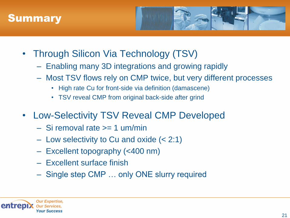
Summary
• Through Silicon Via Technology (TSV)
– Enabling many 3D integrations and growing rapidly
– Most TSV flows rely on CMP twice, but very different processes
• High rate Cu for front-side via definition (damascene)
• TSV reveal CMP from original back-side after grind
• Low-Selectivity TSV Reveal CMP Developed
– Si removal rate >= 1 um/min
– Low selectivity to Cu and oxide (< 2:1)
– Excellent topography (<400 nm)
– Excellent surface finish
– Single step CMP … only ONE slurry required
Our Expertise,
Our Services,
Your Success
THANK YOU !
• For additional information, please contact:
Robert L. Rhoades, Ph.D.
Entrepix, Inc.
Chief Technology Officer
+1.602.426.8668
22

Our Expertise,
Our Services,
Your Success
Appendix
• BACKUP SLIDES TIME PERMITS
23

Our Expertise,
Our Services,
Your Success 24
TSV CMP Issues
• Design rule consistency / standardization
• Incoming variation at CMP
• Uniformity
• Selectivity control
• Plug recess/protrusion
• Throughput
• Repeatability
• Cost per unit operation (slurry, pad life, etc.)

Our Expertise,
Our Services,
Your Success
Design Rules
• Via size
– Determines etch aspect ratio and plating thickness
– Electrical requirements drive minimum size
• Via spacing / pattern density
– Wide variation causes CMP local uniformity issues
– High density of vias weakens mechanical strength
• Feature offsets and tolerances
– Direct impact on die-to-die or wfr-to-wfr alignments
• Via recess and allowed variation
– Design specs must be kept realistic with process capability
25

Our Expertise,
Our Services,
Your Success
Incoming Variation
• Plating thickness variation
– Especially for thicker depositions above 20um
• Etch depth variation
– Range of TSV exposure from opposite side
• TTV from grind or other thinning process
– Determines range of Si to be removed to expose
TSV’s and/or amount of protrusion after exposure
26

Our Expertise,
Our Services,
Your Success
CMP Uniformity
• Clearing behavior at CMP driven by 2 factors:
CMP uniformity and deposition uniformity
• TSV is not generally as sensitive as interconnect … but
– Effects are exaggerated with very thick depositions and long
polish times (compared to interconnect)
– Customers prefer older (depreciated) equipment in packaging
area which may not have as much control as fab tools
27

Our Expertise,
Our Services,
Your Success
Selectivity Control
• Integration determines what materials are being
polished and what are stop layers
– Barrier metal is not universal
– Stop layer options: Barrier, oxide, Si, other?
• Selectivity is mostly driven by the slurry
• Custom formulations can be finely optimized, but
tunability allows broader industry solutions
• Each change in integration can have a huge impact on
CMP constraints for selectivity
28

Our Expertise,
Our Services,
Your Success
Recess/Protrusion
• Factors that drive recess/protrusion
– Selectivity among exposed materials
– Material integrity of core portion of TSV
– Overpolish time required to clear all areas of wafer
• Balance is required
– Too much recess Open contacts
– Too much protrusion Mechanical stress or poor bonding
in some integrations (not as critical for solder bumps)
• Overly tight constraints can easily lead to excess
development costs and difficulty meeting timelines
29

Our Expertise,
Our Services,
Your Success
CMP Variation
• Familiar Sources
– Slurry (pH, particles, etc.)
– Pads
– Conditioning disks
– Wear during pad life
– Test wafer vs product wafer
• Less obvious
– Contamination
– Distribution system
– Pumps & filters
– Slurry dispense location
– Source of H2O2
– Head rebuild technique
– DI water temperature
– Metrology instability (Are you
chasing a ghost?)
– Bake/anneal sensitivity
– Barrier metal grain structure
– Pattern density / layout
30
Others?

Our Expertise,
Our Services,
Your Success
Throughput
• Most TSV processes involve very thick films
– Leads to long polish times at CMP
• Suppliers are focused on high rate slurries
– First generation about 1-1.5 um/min
– Second generation claiming 3-4 um/min
– Via recess can be a challenge at very high rates
• Multi-wafer tools can be an advantage
31

Our Expertise,
Our Services,
Your Success
Repeatability
• Critical in HVM
– Often overlooked or downplayed in development
• High rate slurries tend to be more vulnerable to
contaminants, mix ratios, etc.
• Endpoint can help absorb variations, but has a
few quirks as well
32

Our Expertise,
Our Services,
Your Success
Cost Factors
• Development Cost Factors
– Materials choices and availability
– Number of design cycles
– Speed of implementation
• Manufacturing Cost Factors
– Direct Consumables: Pads, slurries, pad life, etc.
– Plating thickness
– Throughput (drives # of tools and capital cost)
– Yield and scrap rate
33