TS 138 101-1 - V15.3.0 - 5G; NR; User Equipment (UE) radio ... · ETSI 3GPP TS 38.101-1 version...
223
ETSI TS 138 101-1 V15.3.0 (2018-10) 5G; NR; User Equipment (UE) radio transmission and reception; Part 1: Range 1 Standalone (3GPP TS 38.101-1 version 15.3.0 Release 15) TECHNICAL SPECIFICATION
Transcript of TS 138 101-1 - V15.3.0 - 5G; NR; User Equipment (UE) radio ... · ETSI 3GPP TS 38.101-1 version...

ETSI TS 138 101-1 V15.3.0 (2018-10)
5G; NR;
User Equipment (UE) radio transmission and reception; Part 1: Range 1 Standalone
(3GPP TS 38.101-1 version 15.3.0 Release 15)
TECHNICAL SPECIFICATION

ETSI
ETSI TS 138 101-1 V15.3.0 (2018-10)13GPP TS 38.101-1 version 15.3.0 Release 15
Reference RTS/TSGR-0438101-1vf30
Keywords 5G
ETSI
650 Route des Lucioles F-06921 Sophia Antipolis Cedex - FRANCE
Tel.: +33 4 92 94 42 00 Fax: +33 4 93 65 47 16
Siret N° 348 623 562 00017 - NAF 742 C
Association à but non lucratif enregistrée à la Sous-Préfecture de Grasse (06) N° 7803/88
Important notice
The present document can be downloaded from: http://www.etsi.org/standards-search
The present document may be made available in electronic versions and/or in print. The content of any electronic and/or print versions of the present document shall not be modified without the prior written authorization of ETSI. In case of any
existing or perceived difference in contents between such versions and/or in print, the only prevailing document is the print of the Portable Document Format (PDF) version kept on a specific network drive within ETSI Secretariat.
Users of the present document should be aware that the document may be subject to revision or change of status. Information on the current status of this and other ETSI documents is available at
https://portal.etsi.org/TB/ETSIDeliverableStatus.aspx
If you find errors in the present document, please send your comment to one of the following services: https://portal.etsi.org/People/CommiteeSupportStaff.aspx
Copyright Notification
No part may be reproduced or utilized in any form or by any means, electronic or mechanical, including photocopying and microfilm except as authorized by written permission of ETSI.
The content of the PDF version shall not be modified without the written authorization of ETSI. The copyright and the foregoing restriction extend to reproduction in all media.
© ETSI 2018.
All rights reserved.
DECTTM, PLUGTESTSTM, UMTSTM and the ETSI logo are trademarks of ETSI registered for the benefit of its Members. 3GPPTM and LTETM are trademarks of ETSI registered for the benefit of its Members and
of the 3GPP Organizational Partners. oneM2M logo is protected for the benefit of its Members.
GSM® and the GSM logo are trademarks registered and owned by the GSM Association.

ETSI
ETSI TS 138 101-1 V15.3.0 (2018-10)23GPP TS 38.101-1 version 15.3.0 Release 15
Intellectual Property Rights Essential patents
IPRs essential or potentially essential to normative deliverables may have been declared to ETSI. The information pertaining to these essential IPRs, if any, is publicly available for ETSI members and non-members, and can be found in ETSI SR 000 314: "Intellectual Property Rights (IPRs); Essential, or potentially Essential, IPRs notified to ETSI in respect of ETSI standards", which is available from the ETSI Secretariat. Latest updates are available on the ETSI Web server (https://ipr.etsi.org/).
Pursuant to the ETSI IPR Policy, no investigation, including IPR searches, has been carried out by ETSI. No guarantee can be given as to the existence of other IPRs not referenced in ETSI SR 000 314 (or the updates on the ETSI Web server) which are, or may be, or may become, essential to the present document.
Trademarks
The present document may include trademarks and/or tradenames which are asserted and/or registered by their owners. ETSI claims no ownership of these except for any which are indicated as being the property of ETSI, and conveys no right to use or reproduce any trademark and/or tradename. Mention of those trademarks in the present document does not constitute an endorsement by ETSI of products, services or organizations associated with those trademarks.
Foreword This Technical Specification (TS) has been produced by ETSI 3rd Generation Partnership Project (3GPP).
The present document may refer to technical specifications or reports using their 3GPP identities, UMTS identities or GSM identities. These should be interpreted as being references to the corresponding ETSI deliverables.
The cross reference between GSM, UMTS, 3GPP and ETSI identities can be found under http://webapp.etsi.org/key/queryform.asp.
Modal verbs terminology In the present document "shall", "shall not", "should", "should not", "may", "need not", "will", "will not", "can" and "cannot" are to be interpreted as described in clause 3.2 of the ETSI Drafting Rules (Verbal forms for the expression of provisions).
"must" and "must not" are NOT allowed in ETSI deliverables except when used in direct citation.

ETSI
ETSI TS 138 101-1 V15.3.0 (2018-10)33GPP TS 38.101-1 version 15.3.0 Release 15
Contents Intellectual Property Rights ................................................................................................................................ 2
Foreword ............................................................................................................................................................. 2
Modal verbs terminology .................................................................................................................................... 2
Foreword ........................................................................................................................................................... 10
1 Scope ...................................................................................................................................................... 11
2 References .............................................................................................................................................. 11
3 Definitions, symbols and abbreviations ................................................................................................. 11
3.1 Definitions ........................................................................................................................................................ 11
3.2 Symbols ............................................................................................................................................................ 12
3.3 Abbreviations ................................................................................................................................................... 14
4 General ................................................................................................................................................... 15
4.1 Relationship between minimum requirements and test requirements .............................................................. 15
4.2 Applicability of minimum requirements .......................................................................................................... 15
4.3 Specification suffix information ....................................................................................................................... 15
5 Operating bands and channel arrangement ............................................................................................. 16
5.1 General ............................................................................................................................................................. 16
5.2 Operating bands ................................................................................................................................................ 16
5.2A Operating bands for CA ................................................................................................................................... 17
5.2A.1 Intra-band CA ............................................................................................................................................. 17
5.2A.2 Inter-band CA ............................................................................................................................................. 17
5.2B Operating bands for DC ................................................................................................................................... 18
5.2B.1 General ........................................................................................................................................................ 18
5.2C Operating band combination for SUL .............................................................................................................. 18
5.3 UE channel bandwidth ..................................................................................................................................... 19
5.3.1 General ........................................................................................................................................................ 19
5.3.2 Maximum transmission bandwidth configuration ...................................................................................... 19
5.3.3 Minimum guardband and transmission bandwidth configuration ............................................................... 19
5.3.4 RB alignment with different numerologies ................................................................................................. 20
5.3.5 UE channel bandwidth per operating band ................................................................................................. 21
5.3.6 Asymmetric channel bandwidths ................................................................................................................ 24
5.3A UE channel bandwidth for CA ......................................................................................................................... 25
5.3A.1 General ........................................................................................................................................................ 25
5.3A.2 Maximum transmission bandwidth configuration for CA .......................................................................... 25
5.3A.3 Minimum guardband and transmission bandwidth configuration for CA .................................................. 25
5.3A.4 RB alignment with different numerologies for CA..................................................................................... 27
5.3A.5 UE channel bandwidth per operating band for CA ..................................................................................... 27
5.4 Channel arrangement ........................................................................................................................................ 27
5.4.1 Channel spacing .......................................................................................................................................... 27
5.4.1.1 Channel spacing for adjacent NR carriers ............................................................................................. 27
5.4.2 Channel raster ............................................................................................................................................. 28
5.4.2.1 NR-ARFCN and channel raster............................................................................................................. 28
5.4.2.2 Channel raster to resource element mapping......................................................................................... 28
5.4.2.3 Channel raster entries for each operating band ..................................................................................... 28
5.4.3 Synchronization raster ................................................................................................................................ 29
5.4.3.1 Synchronization raster and numbering .................................................................................................. 29
5.4.3.3 Synchronization raster entries for each operating band......................................................................... 30
5.4A Channel arrangement for CA............................................................................................................................ 32
5.4A.1 Channel spacing for CA .............................................................................................................................. 32
5.4A.2 Channel raster for CA ................................................................................................................................. 32
5.4A.3 Synchronization raster for CA .................................................................................................................... 32
5.4A.4 Tx-Rx frequency separation for CA............................................................................................................ 32
5.5 Configurations .................................................................................................................................................. 33
5.5A Configurations for CA ...................................................................................................................................... 33
5.5A.1 Configurations for intra-band contiguous CA............................................................................................. 33

ETSI
ETSI TS 138 101-1 V15.3.0 (2018-10)43GPP TS 38.101-1 version 15.3.0 Release 15
5.5A.2 Configurations for intra-band non-contiguous CA ..................................................................................... 35
5.5A.3 Configurations for inter-band CA ............................................................................................................... 36
5.5B Configurations for DC ...................................................................................................................................... 38
5.5C Configurations for SUL .................................................................................................................................... 38
6 Transmitter characteristics ..................................................................................................................... 39
6.1 General ............................................................................................................................................................. 39
6.2 Transmitter power ............................................................................................................................................ 39
6.2.1 UE maximum output power ........................................................................................................................ 39
6.2.2 UE maximum output power reduction ........................................................................................................ 40
6.2.3 UE additional maximum output power reduction ....................................................................................... 41
6.2.3.1 General .................................................................................................................................................. 41
6.2.3.2 A-MPR for NS_04 ................................................................................................................................ 44
6.2.3.3 A-MPR for NS_10 ................................................................................................................................ 46
6.2.3.4 A-MPR for NS_05 ................................................................................................................................ 47
6.2.3.5 A-MPR for NS_40 ................................................................................................................................ 48
6.2.3.6 A-MPR for NS_08 ................................................................................................................................ 48
6.2.3.7 A-MPR for NS_03 ................................................................................................................................ 50
6.2.3.8 A-MPR for NS_37 ................................................................................................................................ 50
6.2.3.9 A-MPR for NS_38 ................................................................................................................................ 51
6.2.3.10 A-MPR for NS_39 ................................................................................................................................ 51
6.2.3.11 A-MPR for NS_41 ................................................................................................................................ 52
6.2.3.12 A-MPR for NS_42 ................................................................................................................................ 52
6.2.4 Configured transmitted power .................................................................................................................... 53
6.2A Transmitter power for CA ................................................................................................................................ 54
6.2A.1 UE maximum output power for CA ............................................................................................................ 54
6.2A.1.1 UE maximum output power for Intra-band contiguous CA .................................................................. 54
6.2A.1.1 UE maximum output power for Intra-band non-contiguous CA ........................................................... 54
6.2A.1.3 UE maximum output power for Inter-band CA .................................................................................... 54
6.2A.2 UE maximum output power reduction for CA ............................................................................................ 55
6.2A.2.1 UE maximum output power reduction forIntra-band contiguous CA .................................................. 55
6.2A.2.2 UE maximum output power reduction for Intra-band non-contiguous CA ........................................... 55
6.2A.2.3 UE maximum output power reduction for Inter-band CA .................................................................... 55
6.2A.3 UE additional maximum output power reduction for CA ........................................................................... 55
6.2A.3.1.1 UE additional maximum output power reduction for Intra-band contiguous CA............................ 55
6.2A.3.1.2 UE additional maximum output power reduction for Intra-band non-contiguous CA .................... 55
6.2A.3.1.3 UE additional maximum output power reduction for Inter-band CA .............................................. 55
6.2A.4 Configured output power for CA ................................................................................................................ 55
6.2A.4.1 Configured transmitted power level ...................................................................................................... 55
6.2A.4.1.1 Configured transmitted power for Intra-band contiguous CA ......................................................... 55
6.2A.4.1.2 Configured transmitted power for Intra-band non-contiguous CA .................................................. 55
6.2A.4.1.3 Configured transmitted power for Inter-band CA ........................................................................... 55
6.2A.4.2 ΔTIB,c for CA ......................................................................................................................................... 57
6.2A.4.2.1 ΔTIB,c for Intra-band contiguous CA ............................................................................................... 57
6.2A.4.2.2 ΔTIB,c for Intra-band non-contiguous CA ........................................................................................ 57
6.2A.4.2.3 ΔTIB,c for Inter-band CA .................................................................................................................. 57
6.2B Transmitter power for DC ................................................................................................................................ 58
6.2C Transmitter power for SUL .............................................................................................................................. 58
6.2C.1 Configured transmitted power for SUL ...................................................................................................... 58
6.2C.2 ΔTIB,c ........................................................................................................................................................... 58
6.2D Transmitter power for UL-MIMO .................................................................................................................... 59
6.2D.1 UE maximum output power for UL-MIMO ............................................................................................... 59
6.2D.2 UE maximum output power reduction for UL-MIMO ............................................................................... 59
6.2D.3 UE additional maximum output power reduction for UL-MIMO .............................................................. 59
6.2D.4 Configured transmitted power for UL-MIMO ............................................................................................ 59
6.3 Output power dynamics .................................................................................................................................... 60
6.3.1 Minimum output power .............................................................................................................................. 60
6.3.2 Transmit OFF power ................................................................................................................................... 61
6.3.3 Transmit ON/OFF time mask ..................................................................................................................... 61
6.3.3.1 General .................................................................................................................................................. 61
6.3.3.2 General ON/OFF time mask ................................................................................................................. 62
6.3.3.3 Transmit power time mask for slot and short or subslot boundaries ..................................................... 62

ETSI
ETSI TS 138 101-1 V15.3.0 (2018-10)53GPP TS 38.101-1 version 15.3.0 Release 15
6.3.3.4 PRACH time mask ................................................................................................................................ 62
6.3.3.5 Void....................................................................................................................................................... 63
6.3.3.6 SRS time mask ...................................................................................................................................... 63
6.3.3.7 PUSCH-PUCCH and PUSCH-SRS time masks ................................................................................... 65
6.3.3.8 Transmit power time mask for consecutive slot or long subslot transmission and short subslot transmission boundaries ........................................................................................................................ 65
6.3.3.9 Transmit power time mask for consecutive short subslot transmissions boundaries ........................... 65
6.3.4 Power control .............................................................................................................................................. 66
6.3.4.1 General .................................................................................................................................................. 66
6.3.4.2 Absolute power tolerance ...................................................................................................................... 66
6.3.4.3 Relative power tolerance ....................................................................................................................... 66
6.3.4.4 Aggregate power tolerance.................................................................................................................... 67
6.3A Output power dynamics for CA ....................................................................................................................... 67
6.3A.1 Minimum output power for CA .................................................................................................................. 67
6.3A.1.1 Minimum output power for intra-band contiguous CA ......................................................................... 67
6.3A.1.2 Minimum output power for intra-band non-contiguous CA ................................................................. 67
6.3A.1.3 Minimum output power for inter-band CA ........................................................................................... 67
6.3A.2 Transmit OFF power for CA....................................................................................................................... 67
6.3A.2.1 Transmit OFF power for intra-band contiguous CA ............................................................................. 67
6.3A.2.2 Transmit OFF power for intra-band non-contiguous CA ...................................................................... 67
6.3A.2.3 Transmit OFF power for inter-band CA................................................................................................ 67
6.3A.3 Transmit ON/OFF time mask for CA ......................................................................................................... 68
6.3A.3.1 Transmit ON/OFF time mask for intra-band contiguous CA ................................................................ 68
6.3A.3.2 Transmit ON/OFF time mask for intra-band non-contiguous CA ........................................................ 68
6.3A.3.3 Transmit ON/OFF time mask for inter-band CA .................................................................................. 68
6.3A.4 Power control for CA .................................................................................................................................. 68
6.3A.4.1 Power control for intra-band contiguous CA ........................................................................................ 68
6.3A.4.2 Power control for intra-band non-contiguous CA ................................................................................. 68
6.3A.4.3 Power control for inter-band CA ........................................................................................................... 68
6.3D Output power dynamics for UL-MIMO ........................................................................................................... 68
6.3D.1 Minimum output power for UL-MIMO ...................................................................................................... 68
6.3D.2 Transmit OFF power for UL-MIMO .......................................................................................................... 68
6.3D.3 Transmit ON/OFF time mask for UL-MIMO ............................................................................................. 68
6.3D.4 Power control for UL-MIMO ..................................................................................................................... 68
6.4 Transmit signal quality ..................................................................................................................................... 69
6.4.1 Frequency error ........................................................................................................................................... 69
6.4.2 Transmit modulation quality ....................................................................................................................... 69
6.4.2.1 Error Vector Magnitude ........................................................................................................................ 69
6.4.2.2 Carrier leakage ...................................................................................................................................... 70
6.4.2.3 In-band emissions ................................................................................................................................. 70
6.4.2.4 EVM equalizer spectrum flatness ......................................................................................................... 71
6.4.2.4.1 Requirements for pi/2 BPSK modulation ........................................................................................ 72
6.4A Transmit signal quality for CA ......................................................................................................................... 73
6.4A.1 Frequency error for CA ............................................................................................................................... 73
6.4A.1.1 Frequency error for intra-band contiguous CA ..................................................................................... 73
6.4A.1.2 Frequency error for intra-band non-contiguous CA .............................................................................. 73
6.4A.1.3 Frequency error for inter-band CA ........................................................................................................ 73
6.4A.2 Transmit modulation quality for CA ........................................................................................................... 73
6.4A.2.1 Frequency error for intra-band contiguous CA ..................................................................................... 73
6.4A.2.2 Frequency error for intra-band non-contiguous CA .............................................................................. 73
6.4A.2.3 Frequency error for inter-band CA ........................................................................................................ 73
6.4D Transmit signal quality for UL-MIMO ............................................................................................................ 74
6.4D.1 Frequency error for UL-MIMO .................................................................................................................. 74
6.4D.2 Transmit modulation quality for UL-MIMO .............................................................................................. 74
6.4D.3 Time alignment error for UL-MIMO .......................................................................................................... 74
6.4D.4 Requirements for coherent UL MIMO ....................................................................................................... 75
6.5 Output RF spectrum emissions ......................................................................................................................... 75
6.5.1 Occupied bandwidth ................................................................................................................................... 75
6.5.2 Out of band emission .................................................................................................................................. 75
6.5.2.1 General .................................................................................................................................................. 75
6.5.2.2 Spectrum emission mask ....................................................................................................................... 76
6.5.2.3 Additional spectrum emission mask ..................................................................................................... 76

ETSI
ETSI TS 138 101-1 V15.3.0 (2018-10)63GPP TS 38.101-1 version 15.3.0 Release 15
6.5.2.3.1 Requirements for network signalled value "NS_35" ....................................................................... 76
6.5.2.3.2 Requirements for network signalled value "NS_04" ....................................................................... 77
6.5.2.3.3 Requirements for network signalled value "NS_03" ....................................................................... 78
6.5.2.3.4 Requirements for network signalled value "NS_06" ....................................................................... 78
6.5.2.3.5 Requirements for network signalled value "NS_40" ....................................................................... 79
6.5.2.3.6 Requirements for network signalled value “NS_41” ....................................................................... 79
6.5.2.3.7 Requirements for network signalled value "NS_42" ....................................................................... 79
6.5.2.4 Adjacent channel leakage ratio ............................................................................................................. 80
6.5.2.4.1 NR ACLR ........................................................................................................................................ 80
6.5.2.4.2 UTRA ACLR .................................................................................................................................. 80
6.5.3 Spurious emissions ..................................................................................................................................... 81
6.5.3.1 General spurious emissions ................................................................................................................... 81
6.5.3.2 Spurious emissions for UE co-existence ............................................................................................... 82
6.5.3.3 Additional spurious emissions .............................................................................................................. 88
6.5.3.3.1 Requirement for network signalled value "NS_04" ......................................................................... 88
6.5.3.3.3 Requirement for network signalled value “NS_18” ........................................................................ 89
6.5.3.3.5 Requirement for network signalled value “NS_08” ........................................................................ 89
6.5.3.3.6 Requirement for network signalled value “NS_37” ........................................................................ 89
6.5.3.3.7 Requirement for network signalled value “NS_38” ........................................................................ 90
6.5.3.3.8 Requirement for network signalled value “NS_39” ........................................................................ 90
6.5.4 Transmit intermodulation ........................................................................................................................... 90
6.5A Output RF spectrum emissions for CA............................................................................................................. 91
6.5A.1 Occupied bandwidth for CA ....................................................................................................................... 91
6.5A.1.1 Occupied bandwidth for Intra-band contiguous CA ............................................................................. 91
6.5A.1.2 Occupied bandwidth for Intra-band non-contiguous CA ...................................................................... 91
6.5A.1.3 Occupied bandwidth for Inter-band CA ................................................................................................ 91
6.5A.2 Out of band emission for CA ...................................................................................................................... 91
6.5A.2.1 General .................................................................................................................................................. 91
6.5A.2.2 Spectrum emission mask ....................................................................................................................... 91
6.5A.2.2.1 Spectrum emission mask for Intra-band contiguous CA ................................................................. 91
6.5A.2.2.2 Spectrum emission mask for Intra-band non-contiguous CA .......................................................... 91
6.5A.2.2.3 Spectrum emission mask for Inter-band CA.................................................................................... 91
6.5A.2.3 Additional spectrum emission mask ..................................................................................................... 92
6.5A.2.3.1 Additional spectrum emission mask for Intra-band contiguous CA ................................................ 92
6.5A.2.3.2 Additional spectrum emission mask for Intra-band non-contiguous CA......................................... 92
6.5A.2.3.3 Additional spectrum emission mask for Inter-band CA .................................................................. 92
6.5A.2.4 Adjacent channel leakage ratio ............................................................................................................. 92
6.5A.2.4.1 NR ACLR ........................................................................................................................................ 92
6.5A.2.4.1.1 NR ACLR for Intra-band contiguous CA .................................................................................. 92
6.5A.2.4.1.2 NR ACLR for Intra-band non-contiguous CA ........................................................................... 92
6.5A.2.4.1.3 NR ACLR for Inter-band CA..................................................................................................... 92
6.5A.2.4.2 UTRA ACLR .................................................................................................................................. 92
6.5A.2.4.2.1 UTRA ACLR for Intra-band contiguous CA ............................................................................. 92
6.5A.2.4.2.2 UTRA ACLR for Intra-band non-contiguous CA ...................................................................... 92
6.5A.2.4.2.3 UTRA ACLR for Inter-band CA ............................................................................................... 92
6.5A.3 Spurious emission for CA ........................................................................................................................... 92
6.5A.3.1 General spurious emissions ................................................................................................................... 92
6.5A.3.2 Spurious emissions for UE co-existence ............................................................................................... 92
6.5A.3.2.1 Spurious emissions for UE co-existence for Intra-band contiguous CA ......................................... 92
6.5A.3.2.2 Spurious emissions for UE co-existence for Intra-band non-contiguous CA .................................. 92
6.5A.3.2.3 Spurious emissions for UE co-existence for Inter-band CA ............................................................ 92
6.5A.4 Transmit intermodulation for CA ............................................................................................................... 93
6.5A.3.2.1 Transmit intermodulation for Intra-band contiguous CA ................................................................ 93
6.5A.3.2.2 Transmit intermodulation for Intra-band non-contiguous CA ......................................................... 93
6.5A.3.2.3 Transmit intermodulation for Inter-band CA................................................................................... 93
6.5D Output RF spectrum emissions for UL-MIMO ................................................................................................ 93
6.5D.1 Occupied bandwidth for UL-MIMO ........................................................................................................... 93
6.5D.2 Out of band emission for UL-MIMO .......................................................................................................... 94
6.5D.3 Spurious emission for UL-MIMO .............................................................................................................. 94
6.5D.4 Transmit intermodulation for UL-MIMO ................................................................................................... 94
7 Receiver characteristics .......................................................................................................................... 95

ETSI
ETSI TS 138 101-1 V15.3.0 (2018-10)73GPP TS 38.101-1 version 15.3.0 Release 15
7.1 General ............................................................................................................................................................. 95
7.2 Diversity characteristics ................................................................................................................................... 95
7.3 Reference sensitivity ........................................................................................................................................ 95
7.3.1 General ........................................................................................................................................................ 95
7.3.2 Reference sensitivity power level ............................................................................................................... 95
7.3.3 ΔRIB,c ......................................................................................................................................................... 102
7.3A Reference sensitivity for CA .......................................................................................................................... 102
7.3A.1 General ...................................................................................................................................................... 102
7.3A.2 Reference sensitivity power level for CA ................................................................................................. 102
7.3A.2.1 Reference sensitivity power level for Intra-band contiguous CA ....................................................... 102
7.3A.2.2 Reference sensitivity power level for Intra-band non-contiguous CA ................................................ 102
7.3A.2.3 Reference sensitivity power level for Inter-band CA .......................................................................... 102
7.3A.3 ΔRIB,c for CA ............................................................................................................................................ 102
7.3A.3.1 General ................................................................................................................................................ 102
7.3A.3.2 ΔRIB,c for Inter-band CA ...................................................................................................................... 102
7.3A.3.2.1 ΔRIB,c for two bands ...................................................................................................................... 103
7.3A.3.2.2 ΔRIB,c for three bands .................................................................................................................... 103
7.3A.4 Reference sensitivity exceptions due to UL harmonic interference for CA .............................................. 103
7.3A.5 Reference sensitivity exceptions due to intermodulation interference due to 2UL CA ............................ 105
7.3B Reference sensitivity for DC .......................................................................................................................... 106
7.3C Reference sensitivity for SUL ........................................................................................................................ 106
7.3C.1 General ...................................................................................................................................................... 106
7.3C.2 Reference sensitivity power level for SUL ............................................................................................... 106
7.3C.3 ΔRIB,c for SUL .......................................................................................................................................... 107
7.3C.3.1 General ................................................................................................................................................ 107
7.3C.3.2 SUL band combination ....................................................................................................................... 108
7.3C.3.2.1 ΔRIB,c for two bands ...................................................................................................................... 108
7.3D Reference sensitivity for UL-MIMO .............................................................................................................. 108
7.4 Maximum input level ..................................................................................................................................... 108
7.4A Maximum input level for CA ......................................................................................................................... 108
7.4A.1 Maximum input level for Intra-band contiguous CA ................................................................................ 108
7.4A.2 Maximum input level for Intra-band non-contiguous CA ........................................................................ 109
7.4A.3 Maximum input level for Inter-band CA .................................................................................................. 109
7.4D Maximum input level for UL-MIMO ............................................................................................................. 109
7.5 Adjacent channel selectivity ........................................................................................................................... 109
7.5A Adjacent channel selectivity for CA ............................................................................................................... 113
7.5A.1 Adjacent channel selectivity for Intra-band contiguous CA ..................................................................... 113
7.5A.2 Adjacent channel selectivity Intra-band non-contiguous CA ................................................................... 114
7.5A.3 Adjacent channel selectivity Inter-band CA ............................................................................................. 114
7.5D Adjacent channel selectivity for UL-MIMO .................................................................................................. 114
7.6 Blocking characteristics ................................................................................................................................. 114
7.6.1 General ...................................................................................................................................................... 114
7.6.2 In-band blocking ....................................................................................................................................... 115
7.6.3 Out-of-band blocking ................................................................................................................................ 117
7.6.4 Narrow band blocking .............................................................................................................................. 119
7.6A Blocking characteristics for CA ..................................................................................................................... 120
7.6A.1 General ...................................................................................................................................................... 120
7.6A.2 In-band blocking for CA .......................................................................................................................... 120
7.6A.2.1 In-band blocking for Intra-band contiguous CA ............................................................................................... 120
7.6A.2.2 In-band blocking for Intra-band non-contiguous CA .......................................................................... 121
7.6A.2.3 In-band blocking for Inter-band CA .................................................................................................... 121
7.6A.3 Out-of-band blocking for CA.................................................................................................................... 122
7.6A.3.1 Out-of-band blocking for Intra-band contiguous CA ....................................................................................... 122
7.6A.3.2 Out-of-band blocking for Intra-band non-contiguous CA ................................................................................ 123
7.6A.3.3 Out-of-band blocking for Inter-band CA .......................................................................................................... 123
7.6A.4 Narrow band blocking for CA .................................................................................................................. 123
7.6A.4.1 Narrow band blocking for Intra-band contiguous CA ...................................................................................... 123
7.6A.4.2 Narrow band blocking for Intra-band non-contiguous CA ............................................................................... 123
7.6A.4.3 Narrow band blocking for Inter-band CA......................................................................................................... 123
7.6D Blocking characteristics for UL-MIMO ......................................................................................................... 123
7.7 Spurious response ........................................................................................................................................... 123
7.7A Spurious response for CA ............................................................................................................................... 125

ETSI
ETSI TS 138 101-1 V15.3.0 (2018-10)83GPP TS 38.101-1 version 15.3.0 Release 15
7.7A.1 Spurious response for Intra-band contiguous CA ..................................................................................... 125
7.7A.2 Spurious response for Intra-band non-contiguous CA .............................................................................. 125
7.7A.3 Spurious response for Inter-band CA........................................................................................................ 125
7.7D Spurious response for UL-MIMO .................................................................................................................. 125
7.8 Intermodulation characteristics ...................................................................................................................... 125
7.8.1 General ...................................................................................................................................................... 125
7.8.2 Wide band Intermodulation ...................................................................................................................... 126
7.8A Intermodulation characteristics for CA .......................................................................................................... 128
7.8A.1 General ...................................................................................................................................................... 128
7.8A.2 Wide band intermodulation for CA .......................................................................................................... 128
7.8A.2.1 Wide band intermodulation for Intra-band contiguous CA ................................................................. 128
7.8A.2.2 Wide band intermodulation for Intra-band non-contiguous CA ....................................................................... 128
7.8A.2.3 Wide band intermodulation for Inter-band CA ................................................................................................. 128
7.8D Intermodulation characteristics for UL-MIMO .............................................................................................. 128
7.9 Spurious emissions ......................................................................................................................................... 129
7.9A Spurious emissions for CA ............................................................................................................................. 129
7.9A.1 Spurious emissions for Intra-band contiguous CA ................................................................................... 129
7.9A.2 Spurious emissions for Intra-band non-contiguous CA ............................................................................ 129
7.9A.3 Spurious emissions for Inter-band CA ...................................................................................................... 129
Annex A (normative): Measurement channels ................................................................................ 130
A.1 General ................................................................................................................................................. 130
A.2 UL reference measurement channels ................................................................................................... 130
A.2.1 General ........................................................................................................................................................... 130
A.2.2 Reference measurement channels for FDD .................................................................................................... 131
A.2.2.1 DFT-s-OFDM Pi/2-BPSK ........................................................................................................................ 131
A.2.2.2 DFT-s-OFDM QPSK ................................................................................................................................ 134
A.2.2.3 DFT-s-OFDM 16QAM ............................................................................................................................. 137
A.2.2.4 DFT-s-OFDM 64QAM ............................................................................................................................. 140
A.2.2.5 DFT-s-OFDM 256QAM ........................................................................................................................... 143
A.2.2.6 CP-OFDM QPSK ..................................................................................................................................... 146
A.2.2.7 CP-OFDM 16QAM .................................................................................................................................. 149
A.2.2.8 CP-OFDM 64QAM .................................................................................................................................. 152
A.2.2.9 CP-OFDM 256QAM ................................................................................................................................ 155
A.2.3 Reference measurement channels for TDD .................................................................................................... 158
A.2.3.1 DFT-s-OFDM Pi/2-BPSK ........................................................................................................................ 158
A.2.3.2 DFT-s-OFDM QPSK ................................................................................................................................ 161
A.2.3.3 DFT-s-OFDM 16QAM ............................................................................................................................. 164
A.2.3.4 DFT-s-OFDM 64QAM ............................................................................................................................. 167
A.2.3.5 DFT-s-OFDM 256QAM ........................................................................................................................... 170
A.2.3.6 CP-OFDM QPSK ..................................................................................................................................... 173
A.2.3.7 CP-OFDM 16QAM .................................................................................................................................. 176
A.2.3.8 CP-OFDM 64QAM .................................................................................................................................. 179
A.2.3.9 CP-OFDM 256QAM ................................................................................................................................ 182
A.3 DL reference measurement channels ................................................................................................... 185
A.3.1 General ........................................................................................................................................................... 185
A.3.2 DL reference measurement channels for FDD ............................................................................................... 185
A.3.2.1 General ...................................................................................................................................................... 185
A.3.2.2 FRC for receiver requirements for QPSK ................................................................................................. 186
A.3.2.3 FRC for maximum input level for 64QAM .............................................................................................. 189
A.3.2.4 FRC for maximum input level for 256 QAM ........................................................................................... 192
A.3.3 DL reference measurement channels for TDD ............................................................................................... 195
A.3.3.1 General ...................................................................................................................................................... 195
A.3.3.2 FRC for receiver requirements for QPSK ................................................................................................. 195
A.3.3.3 FRC for maximum input level for 64QAM .............................................................................................. 198
A.3.3.4 FRC for maximum input level for 256 QAM ........................................................................................... 201
A.4 CSI reference measurement channels ................................................................................................... 203
A.5 OFDMA Channel Noise Generator (OCNG) ....................................................................................... 203
A.5.1 OCNG Patterns for FDD ................................................................................................................................ 203

ETSI
ETSI TS 138 101-1 V15.3.0 (2018-10)93GPP TS 38.101-1 version 15.3.0 Release 15
A.5.1.1 OCNG FDD pattern 1: Generic OCNG FDD Pattern for all unused REs................................................. 203
A.5.2 OCNG Patterns for TDD ................................................................................................................................ 204
A.5.2.1 OCNG TDD pattern 1: Generic OCNG TDD Pattern for all unused REs ................................................ 204
A.6 Void ...................................................................................................................................................... 204
Annex B (informative): Void ............................................................................................................... 205
Annex C (informative): Downlink physical channels ........................................................................ 206
C.1 General ................................................................................................................................................. 206
C.2 Setup ............................................................................................................................................................... 206
C.3 Connection ..................................................................................................................................................... 206
C.3.1 Measurement of Receiver Characteristics ................................................................................................. 206
Annex D (informative): Void ............................................................................................................... 207
Annex E (normative): Environmental conditions ........................................................................... 208
E.1 General ................................................................................................................................................. 208
E.2 Environmental ...................................................................................................................................... 208
E.2.1 Temperature ................................................................................................................................................... 208
E.2.2 Voltage ........................................................................................................................................................... 208
E.2.3 Vibration......................................................................................................................................................... 209
Annex F (normative): Transmit modulation ................................................................................... 210
F.1 Measurement Point ............................................................................................................................... 210
F.2 Basic Error Vector Magnitude measurement ....................................................................................... 210
F.3 Basic in-band emissions measurement ................................................................................................. 210
F.4 Modified signal under test .................................................................................................................... 211
F.5 Window length ..................................................................................................................................... 213
F.5.1 Timing offset .................................................................................................................................................. 213
F.5.2 Window length ............................................................................................................................................... 213
F.5.3 Window length for normal CP ....................................................................................................................... 213
F.5.4 Window length for Extended CP .................................................................................................................... 213
F.5.5 Window length for PRACH ........................................................................................................................... 213
F.6 Averaged EVM .................................................................................................................................... 213
F.7 Spectrum Flatness ................................................................................................................................ 214
Annex G (informative): Void ............................................................................................................... 215
Annex H (informative): Void ............................................................................................................... 215
Annex I (informative): Void ............................................................................................................... 215
Annex J (informative): Change history ............................................................................................. 216
History ............................................................................................................................................................ 222

ETSI
ETSI TS 138 101-1 V15.3.0 (2018-10)103GPP TS 38.101-1 version 15.3.0 Release 15
Foreword This Technical Specification has been produced by the 3rd Generation Partnership Project (3GPP).
The contents of the present document are subject to continuing work within the TSG and may change following formal TSG approval. Should the TSG modify the contents of the present document, it will be re-released by the TSG with an identifying change of release date and an increase in version number as follows:
Version x.y.z
where:
x the first digit:
1 presented to TSG for information;
2 presented to TSG for approval;
3 or greater indicates TSG approved document under change control.
y the second digit is incremented for all changes of substance, i.e. technical enhancements, corrections, updates, etc.
z the third digit is incremented when editorial only changes have been incorporated in the document.

ETSI
ETSI TS 138 101-1 V15.3.0 (2018-10)113GPP TS 38.101-1 version 15.3.0 Release 15
1 Scope The present document establishes the minimum RF requirements for NR User Equipment (UE) operating on frequency Range 1.
2 References The following documents contain provisions which, through reference in this text, constitute provisions of the present document.
References are either specific (identified by date of publication, edition number, version number, etc.) or non-specific.
For a specific reference, subsequent revisions do not apply.
For a non-specific reference, the latest version applies. In the case of a reference to a 3GPP document (including a GSM document), a non-specific reference implicitly refers to the latest version of that document in the same Release as the present document.
[1] 3GPP TR 21.905: "Vocabulary for 3GPP Specifications".
[2] 3GPP TS 38.101-2: "NR; User Equipment (UE) radio transmission and reception; Part 2: Range 2 Standalone".
[3] 3GPP TS 38.101-3: "NR; User Equipment (UE) radio transmission and reception; Part 3: Range 1 and Range 2 Interworking operation with other radios".
[4] 3GPP TS 38.521-1: "NR; User Equipment (UE) conformance specification; Radio transmission and reception; Part 1: Range 1 Standalone".
[5] Recommendation ITU-R M.1545: "Measurement uncertainty as it applies to test limits for the terrestrial component of International Mobile Telecommunications-2000".
[6] 3GPP TS 38.211: "NR; Physical channels and modulation".
[7] 3GPP TS 38.331: "Radio Resource Control (RRC) protocol specification".
[8] 3GPP TS 38.213: "NR; Physical layer procedures for control".
3 Definitions, symbols and abbreviations
3.1 Definitions For the purposes of the present document, the terms and definitions given in 3GPP TR 21.905 [1] and the following apply. A term defined in the present document takes precedence over the definition of the same term, if any, in 3GPP TR 21.905 [1].
Aggregated Channel Bandwidth: The RF bandwidth in which a UE transmits and receives multiple contiguously aggregated carriers.
Carrier aggregation: Aggregation of two or more component carriers in order to support wider transmission bandwidths.
Carrier aggregation band: A set of one or more operating bands across which multiple carriers are aggregated with a specific set of technical requirements.
Carrier aggregation bandwidth class: A class defined by the aggregated transmission bandwidth configuration and maximum number of component carriers supported by a UE.
Carrier aggregation configuration: A combination of CA operating band(s) and CA bandwidth class(es) supported by a UE.

ETSI
ETSI TS 138 101-1 V15.3.0 (2018-10)123GPP TS 38.101-1 version 15.3.0 Release 15
Contiguous carriers: A set of two or more carriers configured in a spectrum block where there are no RF requirements based on co-existence for un-coordinated operation within the spectrum block.
Contiguous resource allocation: A resource allocation of consecutive resource blocks within one carrier or across contiguously aggregated carriers. The gap between contiguously aggregated carriers due to the nominal channel spacing is allowed.
Contiguous spectrum: Spectrum consisting of a contiguous block of spectrum with no sub-block gaps.
Inter-band carrier aggregation: Carrier aggregation of component carriers in different operating bands.
NOTE: Carriers aggregated in each band can be contiguous or non-contiguous.
Intra-band contiguous carrier aggregation: Contiguous carriers aggregated in the same operating band.
Intra-band non-contiguous carrier aggregation: Non-contiguous carriers aggregated in the same operating band.
Sub-block: This is one contiguous allocated block of spectrum for transmission and reception by the same UE. There may be multiple instances of sub-blocks within an RF bandwidth.
Sub-block bandwidth: The bandwidth of one sub-block.
Sub-block gap: A frequency gap between two consecutive sub-blocks within an RF bandwidth, where the RF requirements in the gap are based on co-existence for un-coordinated operation.
3.2 Symbols For the purposes of the present document, the following symbols apply:
ΔFGlobal Granularity of the global frequency raster ΔFRaster Band dependent channel raster granularity ΔfOOB Δ Frequency of Out Of Band emission ΔFTX-RX Δ Frequency of default TX-RX separation of the FDD operating band ΔPPowerClass Adjustment to maximum output power for a given power class ΔRB The starting frequency offset between the allocated RB and the measured non-allocated RBΔRIB,c
Allowed reference sensitivity relaxation due to support for inter-band CA operation, for serving cell c
ΔRIB,4R Reference sensitivity adjustment due to support for 4 antenna ports
ΔShift Channel raster offset for SUL
ΔTC Allowed operating band edge transmission power relaxation ΔTC,c Allowed operating band edge transmission power relaxation for serving cell c ΔTIB,c Allowed maximum configured output power relaxation due to support for inter-band CA
operation, for serving cell c ΔTIB,c Allowed maximum configured output power relaxation due to support for inter-band CA
operation, for serving cell c BWChannel Channel bandwidth BWChannel,block Sub-block bandwidth, expressed in MHz. BWChannel,block= Fedge,block,high- Fedge,block,low BWChannel_CA Aggregated channel bandwidth, expressed in MHz BWChannel,max Maximum channel bandwidth supported among all bands in a release BWGB max( BWGB,Channel(k) ) BWGB,block,low The minimum guardband for the lowest assigned component carrier within a sub-block BWGB,block,high The minimum guardband for the highest assigned component carrier within a sub-block BWGB,Channel(k) Minimum guard band defined in sub-clause 5.3A.1 of carrier k BWDL Channel bandwidth for DL BWUL Channel bandwidth for UL BWinterferer Bandwidth of the interferer Ceil(x) Rounding upwards; ceil(x) is the smallest integer such that ceil(x) ≥ x Floor(x) Rounding downwards; floor(x) is the greatest integer such that floor(x) ≤ x FC RF reference frequency on the channel raster, given in table 5.4.2.2-1 FC,block, high Fc of the highest transmitted/received carrier in a sub-block
FC,block, low Fc of the lowest transmitted/received carrier in a sub-block FC,low The Fc of the lowest carrier, expressed in MHz FC,high The Fc of the highest carrier, expressed in MHz

ETSI
ETSI TS 138 101-1 V15.3.0 (2018-10)133GPP TS 38.101-1 version 15.3.0 Release 15
FDL_low The lowest frequency of the downlink operating band FDL_high The highest frequency of the downlink operating band FUL_low The lowest frequency of the uplink operating band FUL_high The highest frequency of the uplink operating band Fedge,block,low The lower sub-block edge, where Fedge,block,low = FC,block,low - Foffset, low.
Fedge,block,high The upper sub-block edge, where Fedge,block,high = FC,block,high + Foffset, high.
Fedge_low The lower edge of aggregated channel bandwidth, expressed in MHz. Fedge,low = FC,low - Foffset,low. Fedge_high The higher edge of aggregated channel bandwidth, expressed in MHz. Fedge,high = FC,high + Foffset,high. FInterferer (offset) Frequency offset of the interferer (between the center frequency of the interferer and the carrier
frequency of the carrier measured) FInterferer Frequency of the interferer FIoffset Frequency offset of the interferer (between the center frequency of the interferer and the closest
edge of the carrier measured) Foffset Frequency offset from FC_high to the higher edge or FC_low to the lower edge. Foffset,block,low Separation between lower edge of a sub-block and the center of the lowest component carrier
within the sub-block
Foffset,block,high Separation between higher edge of a sub-block and the center of the highest component carrier within the sub-block
Foffset,high Frequency offset from FC,high to the upper UE RF Bandwidth edge, Foffset,low Frequency offset from FC,low to the lower UE RF Bandwidth edge, FOOB The boundary between the NR out of band emission and spurious emission domains FREF RF reference frequency FREF-Offs Offset used for calculating FREF FREF,Shift RF reference frequency for Supplementary Uplink (SUL) bands Fuw (offset) The frequency separation of the center frequency of the carrier closest to the interferer and the
center frequency of the interferer GBChannel Minimum guard band defined in sub-clause 5.3.3 LCRB Transmission bandwidth which represents the length of a contiguous resource block allocation
expressed in units of resources blocks Max() The largest of given numbers Min() The smallest of given numbers
PRBn Physical resource block number
NRACLR NR ACLR NRB Transmission bandwidth configuration, expressed in units of resource blocks NRB,block,low The transmission bandwidth configurations for the lowest assigned component carrier within the
sub-block NRB,block,high The transmission bandwidth configurations for the highest assigned component carrier within the
sub-block NRB,low The transmission bandwidth configurations according to Table 5.3.2-1 for the lowest assigned
component carrier in section 5.3A.1 NRB,high The transmission bandwidth configurations according to Table 5.3.2-1 for the highest assigned
component carrier in section 5.3A.1 NREF NR Absolute Radio Frequency Channel Number (NR-ARFCN) NREF-Offs Offset used for calculating NREF PCMAX The configured maximum UE output power PCMAX, c The configured maximum UE output power for serving cell c PCMAX, f, c The configured maximum UE output power for carrier f of serving cell c in each slot PEMAX Maximum allowed UE output power signalled by higher layers PEMAX, c Maximum allowed UE output power signalled by higher layers for serving cell c PInterferer Modulated mean power of the interferer PPowerClass PPowerClass is the nominal UE power (i.e., no tolerance) P-MPRc Maximum allowed UE output power reduction for serving cell c PRB The transmitted power per allocated RB, measured in dBm
PUMAX The measured configured maximum UE output power Puw Power of an unwanted DL signal Pw Power of a wanted DL signal RBstart Indicates the lowest RB index of transmitted resource blocks SCSblock,low SCS for the lowest assigned component carrier within the sub-block SCSblock,high SCS for the highest assigned component carrier within the sub-block SCSlow SCS for the lowest assigned component carrier in section 5.3A.1 SCShigh SCS for the highest assigned component carrier in section 5.3A.1

ETSI
ETSI TS 138 101-1 V15.3.0 (2018-10)143GPP TS 38.101-1 version 15.3.0 Release 15
T(PCMAX, f, c) Tolerance for applicable values of PCMAX, f, c for configured maximum UE output power for carrier f of serving cell c
TL,c Absolute value of the lower tolerance for the applicable operating band as specified in section 6.2.1
SSREF SS block reference frequency position UTRAACLR UTRA ACLR
3.3 Abbreviations For the purposes of the present document, the abbreviations given in 3GPP TR 21.905 [1] and the following apply. An abbreviation defined in the present document takes precedence over the definition of the same abbreviation, if any, in 3GPP TR 21.905 [1].
Abbreviation format (EW)
ACLR Adjacent Channel Leakage Ratio ACS Adjacent Channel Selectivity A-MPR Additional Maximum Power Reduction BS Base Station BW Bandwidth BWP Bandwidth Part CA Carrier Aggregation CA_nX-nY Inter-band CA of component carrier(s) in one sub-block within Band X and component carrier(s)
in one sub-block within Band Y where X and Y are the applicable NR operating band CC Component Carriers CP-OFDM Cyclic Prefix-OFDM CW Continuous Wave DC Dual Connectivity DFT-s-OFDM Discrete Fourier Transform-spread-OFDM DM-RS Demodulation Reference Signal DTX Discontinuous TransmissionE-UTRA Evolved UTRA EVM Error Vector Magnitude FR Frequency Range FRC Fixed Reference Channel GSCN Global Synchronization Channel Number IBB In-band Blocking IDFT Inverse Discrete Fourier Transformation ITU-R Radiocommunication Sector of the International Telecommunication Union MBW Measurement bandwidth defined for the protected band MOP Maximum Output Power MPR Allowed maximum power reduction MSD Maximum Sensitivity Degradation NR New Radio NR-ARFCN NR Absolute Radio Frequency Channel Number NS Network Signalling OCNG OFDMA Channel Noise Generator OOB Out-of-band P-MPR Power Management Maximum Power Reduction PRB Physical Resource Block QAM Quadrature Amplitude Modulation RE Resource Element REFSENS Reference Sensitivity RF Radio Frequency RMS Root Mean Square (value) RSRP Reference Signal Receiving PowerRx Receiver SC Single Carrier SCS Subcarrier spacing SDL Supplementary Downlink SEM Spectrum Emission Mask SNR Signal-to-Noise Ratio SRS Sounding Reference SymbolSUL Supplementary uplink
ETSI
ETSI TS 138 101-1 V15.3.0 (2018-10)153GPP TS 38.101-1 version 15.3.0 Release 15
SS Synchronization Symbol TAE Time Alignment Error Tx Transmitter UL-MIMO Uplink Multiple Antenna transmission
4 General
4.1 Relationship between minimum requirements and test requirements The present document is a Single-RAT specification for NR UE, covering RF characteristics and minimum performance requirements. Conformance to the present specification is demonstrated by fulfilling the test requirements specified in the conformance specification 3GPP TS 38.521-1 [4].
The Minimum Requirements given in this specification make no allowance for measurement uncertainty. The test specification TS 38.521-1 [4] defines test tolerances. These test tolerances are individually calculated for each test. The test tolerances are used to relax the minimum requirements in this specification to create test requirements. For some requirements, including regulatory requirements, the test tolerance is set to zero.
The measurement results returned by the test system are compared - without any modification - against the test requirements as defined by the shared risk principle.
The shared risk principle is defined in Recommendation ITU-R M.1545 [5].
4.2 Applicability of minimum requirements a) In this specification the Minimum Requirements are specified as general requirements and additional requirements. Where the Requirement is specified as a general requirement, the requirement is mandated to be met in all scenarios
b) For specific scenarios for which an additional requirement is specified, in addition to meeting the general requirement, the UE is mandated to meet the additional requirements.
c) The spurious emissions power requirements are for the long-term average of the power. For the purpose of reducing measurement uncertainty it is acceptable to average the measured power over a period of time sufficient to reduce the uncertainty due to the statistical nature of the signal
4.3 Specification suffix information Unless stated otherwise the following suffixes are used for indicating at 2nd level subclause, shown in Table 4.3-1.
Table 4.3-1: Definition of suffixes
Clause suffix Variant None Single Carrier
A Carrier Aggregation (CA) B Dual-Connectivity (DC) C Supplement Uplink (SUL) D UL MIMO
A terminal which supports the above features needs to meet both the general requirements and the additional requirement applicable to the additional subclause (suffix A, B, C and D) in clauses 5, 6 and 7. Where there is a difference in requirement between the general requirements and the additional subclause requirements (suffix A, B, C and D) in clauses 5, 6 and 7, the tighter requirements are applicable unless stated otherwise in the additional subclause.
A terminal which supports more than one feature in clauses 5, 6 and 7 shall meet all of the separate corresponding requirements.
For a terminal that supports SUL for the band combination specified in Table 5.2C-1, the current version of the specification assumes the terminal is configured with active transmission either on UL carrier or SUL carrier at any

ETSI
ETSI TS 138 101-1 V15.3.0 (2018-10)163GPP TS 38.101-1 version 15.3.0 Release 15
time in one serving cell and the UE requirements for single carrier shall apply for the active UL or SUL carrier accordingly.
5 Operating bands and channel arrangement
5.1 General The channel arrangements presented in this clause are based on the operating bands and channel bandwidths defined in the present release of specifications.
NOTE: Other operating bands and channel bandwidths may be considered in future releases.
Requirements throughout the RF specifications are in many cases defined separately for different frequency ranges (FR). The frequency ranges in which NR can operate according to this version of the specification are identified as described in Table 5.1-1.
Table 5.1-1: Definition of frequency ranges
Frequency range designation
Corresponding frequency range
FR1 450 MHz – 6000 MHz FR2 24250 MHz – 52600 MHz
The present specification covers FR1 operating bands.
5.2 Operating bands NR is designed to operate in the FR1 operating bands defined in Table 5.2-1.

ETSI
ETSI TS 138 101-1 V15.3.0 (2018-10)173GPP TS 38.101-1 version 15.3.0 Release 15
Table 5.2-1: NR operating bands in FR1
NR operating
band
Uplink (UL) operating band BS receive / UE transmit
FUL_low – FUL_high
Downlink (DL) operating band BS transmit / UE receive
FDL_low – FDL_high
Duplex Mode
n1 1920 MHz – 1980 MHz 2110 MHz – 2170 MHz FDD n2 1850 MHz – 1910 MHz 1930 MHz – 1990 MHz FDD n3 1710 MHz – 1785 MHz 1805 MHz – 1880 MHz FDD n5 824 MHz – 849 MHz 869 MHz – 894 MHz FDD n7 2500 MHz – 2570 MHz 2620 MHz – 2690 MHz FDD n8 880 MHz – 915 MHz 925 MHz – 960 MHz FDD
n12 699 MHz – 716 MHz 729 MHz – 746 MHz FDD n20 832 MHz – 862 MHz 791 MHz – 821 MHz FDD n25 1850 MHz – 1915 MHz 1930 MHz – 1995 MHz FDD n28 703 MHz – 748 MHz 758 MHz – 803 MHz FDD n34 2010 MHz – 2025 MHz 2010 MHz – 2025 MHz TDD n38 2570 MHz – 2620 MHz 2570 MHz – 2620 MHz TDD n39 1880 MHz – 1920 MHz 1880 MHz – 1920 MHz TDD n40 2300 MHz – 2400 MHz 2300 MHz – 2400 MHz TDD n41 2496 MHz – 2690 MHz 2496 MHz – 2690 MHz TDD n50 1432 MHz – 1517 MHz 1432 MHz – 1517 MHz TDD1 n51 1427 MHz – 1432 MHz 1427 MHz – 1432 MHz TDD n66 1710 MHz – 1780 MHz 2110 MHz – 2200 MHz FDD n70 1695 MHz – 1710 MHz 1995 MHz – 2020 MHz FDD n71 663 MHz – 698 MHz 617 MHz – 652 MHz FDD n74 1427 MHz – 1470 MHz 1475 MHz – 1518 MHz FDD n75 N/A 1432 MHz – 1517 MHz SDL n76 N/A 1427 MHz – 1432 MHz SDL n77 3300 MHz – 4200 MHz 3300 MHz – 4200 MHz TDD n78 3300 MHz – 3800 MHz 3300 MHz – 3800 MHz TDD n79 4400 MHz – 5000 MHz 4400 MHz – 5000 MHz TDD n80 1710 MHz – 1785 MHz N/A SUL n81 880 MHz – 915 MHz N/A SUL n82 832 MHz – 862 MHz N/A SUL n83 703 MHz – 748 MHz N/A SUL n84 1920 MHz – 1980 MHz N/A SUL n86 1710 MHz – 1780MHz N/A SUL
NOTE 1: UE that complies with the NR Band n50 minimum requirements in this specification shall also comply with the NR Band n51 minimum requirements.
5.2A Operating bands for CA
5.2A.1 Intra-band CA
NR intra-band contiguous carrier aggregation is designed to operate in the operating bands defined in Table 5.2A.1-1, where all operating bands are within FR1.
Table 5.2A.1-1: Intra-band contiguous CA operating bands in FR1
NR CA Band NR Band (Table 5.2-1)
CA_n77 n77 CA_n78 n78 CA_n79 n79
5.2A.2 Inter-band CA
NR inter-band carrier aggregation is designed to operate in the operating bands defined in Table 5.2A.2-1, where all operating bands are within FR1.

ETSI
ETSI TS 138 101-1 V15.3.0 (2018-10)183GPP TS 38.101-1 version 15.3.0 Release 15
Table 5.2A.2-1: Inter-band CA operating bands involving FR1 (two bands)
NR CA Band NR Band (Table 5.2-1)
CA_n3A-n77A n3, n77 CA_n3A-n78A n3, n78 CA_n3A-n79A n3, n79 CA_n8A-n75A n8, n75 CA n8-n78A n8, n78
CA_n8A-n79A n8, n79 CA_n28A-n75A2 n28, n75 CA_n28A_n78A n28, n78 CA_n41A-n78A n41, n78 CA_n75A-n78A1 n75, n78 CA_n77A-n79A n77, n79 CA_n78A-n79A n78, n79
NOTE 1: Applicable for UE supporting inter-band carrier aggregation with mandatory simultaneous Rx/Tx capability.
NOTE 2: The frequency range in band n28 is restricted for this band combination to 703-733 MHz for the UL and 758-788 MHz for the DL.
5.2B Operating bands for DC
5.2B.1 General
NR dual connectivity is designed to operate in the operating bands defined in Table 5.2B-1, where all operating bands are within FR1.
Table 5.2B-1: Inter-band DC operating bands involving FR1 (two bands)
NR DC Band NR Band (Table 5.2-1)
NOTE: Applicable for UE supporting inter-band dual
connectivity with mandatory simultaneous Rx/Tx capability.
5.2C Operating band combination for SUL NR operation is designed to operate in the operating band combination defined in Table 5.2C-1, where all operating bands are within FR1.

ETSI
ETSI TS 138 101-1 V15.3.0 (2018-10)193GPP TS 38.101-1 version 15.3.0 Release 15
Table 5.2C-1: Operating band combination for SUL in FR1
NR Band combination for SUL
NR Band (Table 5.2-1)
SUL_n78-n802 n78, n80 SUL_n78-n812 n78, n81 SUL_n78-n822 n78, n82 SUL_n78-n832 n78, n83 SUL_n78-n842 n78, n84 SUL_n78-n862 n78, n86 SUL_n79-n802 n79, n80 SUL_n79-n812 n79, n81
NOTE 1: If a UE is configured with both NR UL and NR SUL carriers in a cell, the switching time between NR UL carrier and NR SUL carrier is 0us.
NOTE 2: For UE supporting SUL band combination simultaneous Rx/Tx capability is mandatory.
5.3 UE channel bandwidth
5.3.1 General
The UE channel bandwidth supports a single NR RF carrier in the uplink or downlink at the UE. From a BS perspective, different UE channel bandwidths may be supported within the same spectrum for transmitting to and receiving from UEs connected to the BS. Transmission of multiple carriers to the same UE (CA) or multiple carriers to different UEs within the BS channel bandwidth can be supported.
From a UE perspective, the UE is configured with one or more BWP / carriers, each with its own UE channel bandwidth. The UE does not need to be aware of the BS channel bandwidth or how the BS allocates bandwidth to different UEs.
The placement of the UE channel bandwidth for each UE carrier is flexible but can only be completely within the BS channel bandwidth.
5.3.2 Maximum transmission bandwidth configuration
The maximum transmission bandwidth configuration NRB for each UE channel bandwidth and subcarrier spacing is specified in Table 5.3.2-1.
Table 5.3.2-1: Maximum transmission bandwidth configuration NRB
5.3.3 Minimum guardband and transmission bandwidth configuration
The minimum guardband for each UE channel bandwidth and SCS is specified in Table 5.3.3-1,
Table 5.3.3-1: Minimum guardband for each UE channel bandwidth and SCS (kHz)
SCS (kHz)
5MHz 10MHz 15MHz 20 MHz
25 MHz 30 MHz 40
MHz 50MHz 60 MHz
80 MHz 90 MHz 100
MHz NRB NRB NRB NRB NRB NRB NRB NRB NRB NRB NRB NRB
15 25 52 79 106 133 160 216 270 N/A N/A N/A N/A 30 11 24 38 51 65 78 106 133 162 217 245 273 60 N/A 11 18 24 31 38 51 65 79 107 121 135
SCS (kHz) 5 MHz 10
MHz 15
MHz 20
MHz 25
MHz 30 MHz 40 MHz 50MHz 60
MHz 80 MHz 90 MHz 100 MHz
15 242.5 312.5 382.5 452.5 522.5 592.5 552.5 692.5 N/A N/A N/A N/A 30 505 665 645 805 785 945 905 1045 825 925 885 845 60 N/A 1010 990 1330 1310 1290 1610 1570 1530 1450 1410 1370

ETSI
ETSI TS 138 101-1 V15.3.0 (2018-10)203GPP TS 38.101-1 version 15.3.0 Release 15
NOTE: The minimum guardbands have been calculated using the following equation: (CHBW x 1000 (kHz) - RB value x SCS x 12) / 2 - SCS/2, where RB values are from Table 5.3.2-1.
Figure 5.3.3-1: Void
The number of RBs configured in any channel bandwidth shall ensure that the minimum guardband specified in this clause is met.
Figure 5.3.3-2: UE PRB utilization
In the case that multiple numerologies are multiplexed in the same symbol due to BS transmission of SSB, the minimum guardband on each side of the carrier is the guardband applied at the configured channel bandwidth for the numerology that is received immediately adjacent to the guard.
If multiple numerologies are multiplexed in the same symbol and the UE channel bandwidth is >50 MHz, the minimum guardband applied adjacent to 15 kHz SCS shall be the same as the minimum guardband defined for 30 kHz SCS for the same UE channel bandwidth.
Figure 5.3.3-3 Guard band definition when transmitting multiple numerologies
NOTE: Figure 5.3.3-3 is not intended to imply the size of any guard between the two numerologies. Inter-numerology guard band within the carrier is implementation dependent.
5.3.4 RB alignment with different numerologies
For each numerology, its common resource blocks are specified in Section 4.4.4.3 in [9], and the starting point of its transmission bandwidth configuration on the common resource block grid for a given channel bandwidth is indicated by an offset to “Reference point A” in the unit of the numerology. The indicated transmission bandwidth configuration must fulfil the minimum guardband requirement specified in Section 5.3.3.

ETSI
ETSI TS 138 101-1 V15.3.0 (2018-10)213GPP TS 38.101-1 version 15.3.0 Release 15
5.3.5 UE channel bandwidth per operating band
The requirements in this specification apply to the combination of channel bandwidths, SCS and operating bands shown in Table 5.3.5-1. The transmission bandwidth configuration in Table 5.3.2-1 shall be supported for each of the specified channel bandwidths. The channel bandwidths are specified for both the TX and RX path.

ETSI
ETSI TS 138 101-1 V15.3.0 (2018-10)223GPP TS 38.101-1 version 15.3.0 Release 15
Table 5.3.5-1 Channel bandwidths for each NR band

ETSI
ETSI TS 138 101-1 V15.3.0 (2018-10)233GPP TS 38.101-1 version 15.3.0 Release 15
NR band / SCS / UE Channel bandwidth NR
Band SCS kHz
5 MHz
101,2 MHz
152 MHz
202 MHz
252 MHz
30 MHz
40 MHz
50 MHz
60 MHz
80 MHz
90 MHz
100 MHz
n1 15 Yes Yes Yes Yes 30 Yes Yes Yes 60 Yes Yes Yes
n2 15
Yes Yes Yes Yes 30 Yes Yes Yes 60 Yes Yes Yes
n3 15 Yes Yes Yes Yes Yes Yes 30 Yes Yes Yes Yes Yes 60 Yes Yes Yes Yes Yes
n5 15 Yes Yes Yes Yes 30 Yes Yes Yes 60
n7 15 Yes Yes Yes Yes 30 Yes Yes Yes 60 Yes Yes Yes
n8 15 Yes Yes Yes Yes 30 Yes Yes Yes 60
n12 15 Yes Yes Yes 30 Yes Yes 60
n20 15 Yes Yes Yes Yes 30 Yes Yes Yes 60
n25 15 Yes Yes Yes Yes 30 Yes Yes Yes 60 Yes Yes Yes
n28 15 Yes Yes Yes Yes 30 Yes Yes Yes 60
n34 15 Yes Yes Yes 30 Yes Yes 60 Yes Yes
n38 15 Yes Yes Yes Yes 30 Yes Yes Yes 60 Yes Yes Yes
n39 15 Yes Yes Yes Yes Yes Yes Yes 30 Yes Yes Yes Yes Yes Yes 60 Yes Yes Yes Yes Yes Yes
n40 15 Yes Yes Yes Yes Yes Yes Yes Yes 30 Yes Yes Yes Yes Yes Yes Yes Yes Yes 60 Yes Yes Yes Yes Yes Yes Yes Yes Yes
n41 15 Yes Yes Yes Yes Yes 30 Yes Yes Yes Yes Yes Yes Yes Yes Yes 60 Yes Yes Yes Yes Yes Yes Yes Yes Yes
n50 15 Yes Yes Yes Yes Yes Yes 30 Yes Yes Yes Yes Yes Yes Yes3 60 Yes Yes Yes Yes Yes Yes Yes3
n51 15 Yes 30 60
n66 15 Yes Yes Yes Yes Yes 30 Yes Yes Yes Yes 60 Yes Yes Yes Yes
n70 15 Yes Yes Yes Yes3 Yes3 30 Yes Yes Yes3 Yes3 60 Yes Yes Yes3 Yes3
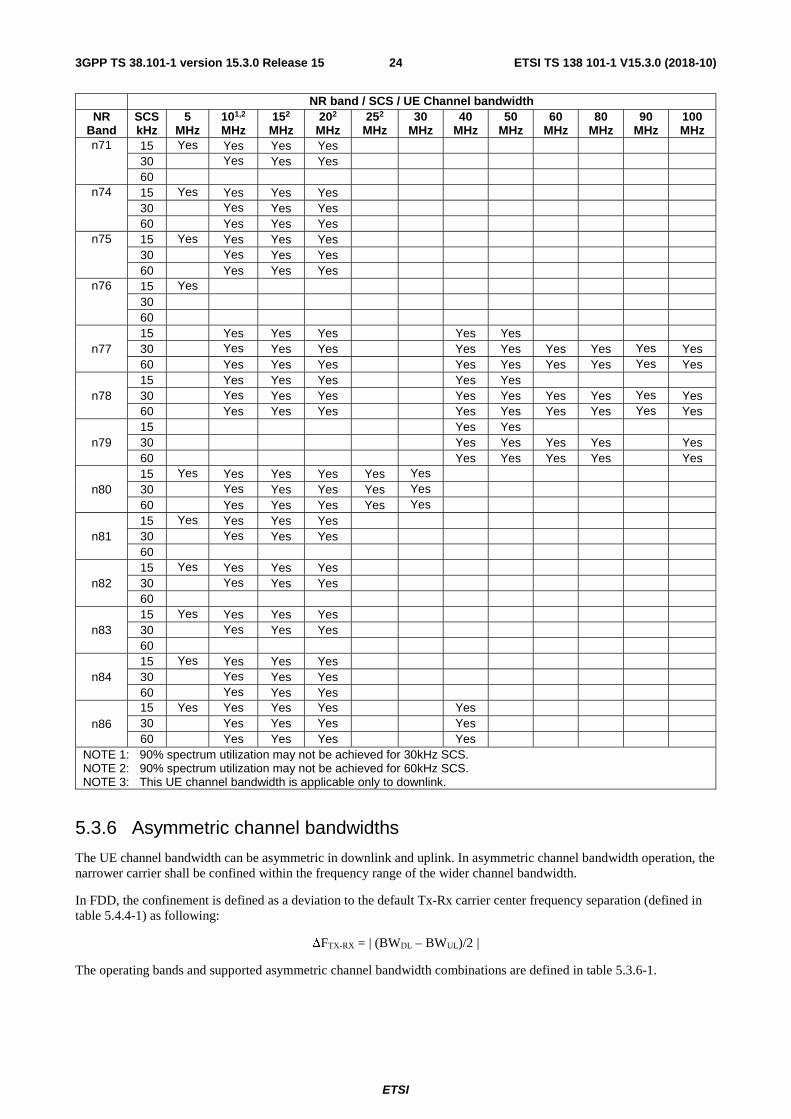
ETSI
ETSI TS 138 101-1 V15.3.0 (2018-10)243GPP TS 38.101-1 version 15.3.0 Release 15
NR band / SCS / UE Channel bandwidth NR
Band SCS kHz
5 MHz
101,2 MHz
152 MHz
202 MHz
252 MHz
30 MHz
40 MHz
50 MHz
60 MHz
80 MHz
90 MHz
100 MHz
n71 15 Yes Yes Yes Yes 30 Yes Yes Yes 60
n74 15 Yes Yes Yes Yes 30 Yes Yes Yes 60 Yes Yes Yes
n75 15 Yes Yes Yes Yes 30 Yes Yes Yes 60 Yes Yes Yes
n76 15 Yes 30 60
n77 15 Yes Yes Yes Yes Yes 30 Yes Yes Yes Yes Yes Yes Yes Yes Yes 60 Yes Yes Yes Yes Yes Yes Yes Yes Yes
n78 15 Yes Yes Yes Yes Yes 30 Yes Yes Yes Yes Yes Yes Yes Yes Yes 60 Yes Yes Yes Yes Yes Yes Yes Yes Yes
n79 15 Yes Yes 30 Yes Yes Yes Yes Yes 60 Yes Yes Yes Yes Yes
n80 15 Yes Yes Yes Yes Yes Yes 30 Yes Yes Yes Yes Yes 60 Yes Yes Yes Yes Yes
n81 15 Yes Yes Yes Yes 30 Yes Yes Yes 60
n82 15 Yes Yes Yes Yes 30 Yes Yes Yes 60
n83 15 Yes Yes Yes Yes 30 Yes Yes Yes 60
n84 15 Yes Yes Yes Yes 30 Yes Yes Yes 60 Yes Yes Yes
n86 15 Yes Yes Yes Yes Yes 30 Yes Yes Yes Yes 60 Yes Yes Yes Yes
NOTE 1: 90% spectrum utilization may not be achieved for 30kHz SCS. NOTE 2: 90% spectrum utilization may not be achieved for 60kHz SCS. NOTE 3: This UE channel bandwidth is applicable only to downlink.
5.3.6 Asymmetric channel bandwidths
The UE channel bandwidth can be asymmetric in downlink and uplink. In asymmetric channel bandwidth operation, the narrower carrier shall be confined within the frequency range of the wider channel bandwidth.
In FDD, the confinement is defined as a deviation to the default Tx-Rx carrier center frequency separation (defined in table 5.4.4-1) as following:
ΔFTX-RX = | (BWDL – BWUL)/2 |
The operating bands and supported asymmetric channel bandwidth combinations are defined in table 5.3.6-1.

ETSI
ETSI TS 138 101-1 V15.3.0 (2018-10)253GPP TS 38.101-1 version 15.3.0 Release 15
Table 5.3.6-1: FDD asymmetric UL and DL channel bandwidth combinations
NR Band Channel
bandwidths for UL (MHz)
Channel bandwidths for DL
(MHz)
n66 5, 10 20, 40
20 40
n70 5 10, 15
5, 10, 15 20, 25
In TDD, the operating bands and supported asymmetric channel bandwidth combinations are defined in table 5.3.6-2.
Table 5.3.6-2: TDD asymmetric UL and DL channel bandwidth combinations
NR Band Channel bandwidths for UL
(MHz)
Channel bandwidths for DL
(MHz) n50 60 80
5.3A UE channel bandwidth for CA
5.3A.1 General
Figure 5.3A.1-1: Void
Figure 5.3A.1-2: Void
5.3A.2 Maximum transmission bandwidth configuration for CA
For carrier aggregation, the maximum transmission bandwidth configuration is defined per component carrier and the requirement is specified in subclause 5.3.2.
5.3A.3 Minimum guardband and transmission bandwidth configuration for CA
For intra-band contiguous carrier aggregation, Aggregated Channel Bandwidth and Guard Bands are defined as follows, see Figure 5.3A.3-1.
Figure 5.3A.3-1: Definition of Aggregated Channel Bandwidth for intra-band carrier aggregation
The aggregated channel bandwidth, BWChannel_CA, is defined as
FC_low
Lo
wer E
dg
e
Up
per E
dg
e
Lowest Carrier Transmission Bandwidth
Configuration [RB]
FC_high
Foffset_low
Highest Carrier Transmission Bandwidth
Configuration [RB]
Reso
urce b
lock
Aggregated UE Channel Bandwidth, BWchannel_CA [MHz]
Fedge_low Fedge_high
Foffset_high

ETSI
ETSI TS 138 101-1 V15.3.0 (2018-10)263GPP TS 38.101-1 version 15.3.0 Release 15
BWChannel_CA = Fedge,high - Fedge,low (MHz).
The lower bandwidth edge Fedge, low and the upper bandwidth edge Fedge,high of the aggregated channel bandwidth are used as frequency reference points for transmitter and receiver requirements and are defined by
Fedge,low = FC,low - Foffset,low
Fedge,high = FC,high + Foffset,high
The lower and upper frequency offsets depend on the transmission bandwidth configurations of the lowest and highest assigned edge component carrier and are defined as
Foffset,low = (NRB,low*12 + 1)*SCSlow/2 + BWGB (MHz)
Foffset,high = (NRB,high*12 - 1)*SCShigh/2 + BWGB (MHz)
BWGB = max(BWGB,Channel(k))
BWGB,Channel(k) is the minimum guard band defined in sub-clause 5.3.3 of carrier k, while NRB,low and NRB,high are the transmission bandwidth configurations according to Table 5.3.2-1 for the lowest and highest assigned component carrier, respectively.
For intra-band non-contiguous carrier aggregation Sub-block Bandwidth and Sub-block edges are defined as follows, see Figure 5.3A.3-2.
Figure 5.3A.3-2: Definition of sub-block bandwidth for intra-band non-contiguous spectrum
The lower sub-block edge of the Sub-block Bandwidth (BWChannel,block) is defined as
Fedge,block, low = FC,block,low - Foffset,block, low.
The upper sub-block edge of the Sub-block Bandwidth is defined as
Fedge,block,high = FC,block,high + Foffset,block,high.
The Sub-block Bandwidth, BWChannel,block, is defined as follows:
BWChannel,block = Fedge,block,high - Fedge,block,low (MHz)
The lower and upper frequency offsets Foffset,block,low and Foffset,block,high depend on the transmission bandwidth configurations of the lowest and highest assigned edge component carriers within a sub-block and are defined as
Foffset,block,low = (NRB,low*12 + 1)*SCSlow/2 + BWGB,low (MHz)
Foffset,block,high = (NRB,high*12 - 1)*SCShigh/2 + BWGB,high(MHz)
...
Sub block n
Transmission Bandwidth
Configuration of the highest carrier in a
sub-block [RB]
Transmission Bandwidth
Configuration of the lowest carrier in a
sub-block [RB]
Fedge,block n, low FC,block n,high Fedge,block n,high
Foffset,block n,high Foffset,block n,low
FC,block n,low
Sub-block Bandwidth, BWChannel,block n [MHz]
Lo
wer S
ub
-blo
ck Ed
ge
Up
per S
ub
-blo
ck Ed
ge
Reso
urce b
lock
Sub block n+1
Fedge,block n+1, low FC,block n+1,low FC,block n+1,high
Fedge,block n+1,high Foffset,block n+1,high
Sub-block Bandwidth, BWChannel,block n+1 [MHz]
Lo
wer S
ub
-blo
ck Ed
ge
Up
per S
ub
-blo
ck Ed
ge
Transmission Bandwidth
Configuration of the highest carrier in a
sub-block [RB]
Transmission Bandwidth
Configuration of the lowest carrier in a
sub-block [RB]
Reso
urce b
lock

ETSI
ETSI TS 138 101-1 V15.3.0 (2018-10)273GPP TS 38.101-1 version 15.3.0 Release 15
where NRB,low and NRB,high are the transmission bandwidth configurations according to Table 5.3.2-1 for the lowest and highest assigned component carrier within a sub-block, respectively. BWGB,low, BWGB,high are the minimum guard band defined in sub-clause 5.3.3 for the lowest and highest assigned component carrier respectively
The sub-block gap size between two consecutive sub-blocks Wgap is defined as
Wgap = Fedge,block n+1,low - Fedge,block n,high (MHz)
5.3A.4 RB alignment with different numerologies for CA
5.3A.5 UE channel bandwidth per operating band for CA
The requirements for carrier aggregation in this specification are defined for carrier aggregation configurations.
For intra-band contiguous carrier aggregation, a carrier aggregation configuration is a single operating band supporting a carrier aggregation bandwidth class with associated bandwidth combination sets specified in clause 5.5A.1. For each carrier aggregation configuration, requirements are specified for all aggregated channel bandwidths contained in a bandwidth combination set, A UE can indicate support of several bandwidth combination sets per carrier aggregation configuration.For intra-band non-contiguous carrier aggregation, a carrier aggregation configuration is a single operating band supporting two or more sub-blocks, each supporting a carrier aggregation bandwidth class.
For inter-band carrier aggregation, a carrier aggregation configuration is a combination of operating bands, each supporting a carrier aggregation bandwidth class.
Table 5.3A.5-1: CA bandwidth classes
NR CA bandwidth class Aggregated channel bandwidth Number of contiguous CC
Fallback group
A BWChannel_CA ≤ BWChannel,max 1 B 20 MHz ≤ BWChannel_CA ≤ 50 MHz 2 C 100 MHz < BWChannel_CA ≤ 2 x
BWChannel,max 2 1
D 200 MHz < BWChannel_CA ≤ 3 x BWChannel,max
3
E 300 MHz < BWChannel_CA ≤ 4 x BWChannel,max
4
F 50 MHz < BWChannel_CA ≤ 100 MHz 2 2 G 100 MHz < BWChannel_CA ≤ 150 MHz 3 H 150 MHz < BWChannel_CA ≤ 200 MHz 4 I 200 MHz < BWChannel_CA ≤ 250 MHz 5 J 250 MHz < BWChannel_CA ≤ 300 MHz 6 K 300 MHz < BWChannel_CA ≤ 350 MHz 7 L 350 MHz < BWChannel_CA ≤ 400 MHz 8
NOTE: BWChannel, max is maximum channel bandwidth supported among all bands in a release
5.4 Channel arrangement
5.4.1 Channel spacing
5.4.1.1 Channel spacing for adjacent NR carriers
The spacing between carriers will depend on the deployment scenario, the size of the frequency block available and the channel bandwidths. The nominal channel spacing between two adjacent NR carriers is defined as following:
- For NR operating bands with 100 kHz channel raster,
Nominal Channel spacing = (BWChannel(1) + BWChannel(2))/2
- For NR operating bands with 15 kHz channel raster,
Nominal Channel spacing = (BWChannel(1) + BWChannel(2))/2+{-5kHz, 0kHz, 5kHz}

ETSI
ETSI TS 138 101-1 V15.3.0 (2018-10)283GPP TS 38.101-1 version 15.3.0 Release 15
where BWChannel(1) and BWChannel(2) are the channel bandwidths of the two respective NR carriers. The channel spacing can be adjusted depending on the channel raster to optimize performance in a particular deployment scenario.
5.4.2 Channel raster
5.4.2.1 NR-ARFCN and channel raster
The global frequency channel raster defines a set of RF reference frequencies FREF. The RF reference frequency is used in signalling to identify the position of RF channels, SS blocks and other elements.
The global frequency raster is defined for all frequencies from 0 to 100 GHz. The granularity of the global frequency raster is ΔFGlobal.
RF reference frequencies are designated by an NR Absolute Radio Frequency Channel Number (NR-ARFCN) in the range (0.. 2016666) on the global frequency raster. The relation between the NR-ARFCN and the RF reference frequency FREF in MHz is given by the following equation, where FREF-Offs and NRef-Offs are given in table 5.4.2.1-1 and NREF is the NR-ARFCN.
FREF = FREF-Offs + ΔFGlobal (NREF – NREF-Offs)
Table 5.4.2.1-1: NR-ARFCN parameters for the global frequency raster
Frequency range (MHz) ΔFGlobal (kHz) FREF-Offs (MHz) NREF-Offs Range of NREF 0 – 3000 5 0 0 0 – 599999
3000 – 24250 15 3000 600000 600000 – 2016666
The channel raster defines a subset of RF reference frequencies that can be used to identify the RF channel position in the uplink and downlink. The RF reference frequency for an RF channel maps to a resource element on the carrier. For each operating band, a subset of frequencies from the global frequency raster are applicable for that band and forms a channel raster with a granularity ΔFRaster, which may be equal to or larger than ΔFGlobal.
For SUL bands and Bands n1, n2, n3, n5, n7, n8, n20, n28, n66 and n71 defined in Table 5.2-1.
FREF_shift = FREF + Δshift, Δshift=0kHz or 7.5kHz.
where Δshift is signalled by the network in higher layer parameter frequencyShift7p5khz [7].
The mapping between the channel raster and corresponding resource element is given in Section 5.4.2.2. The applicable entries for each operating band are defined in Section 5.4.2.3
5.4.2.2 Channel raster to resource element mapping
The mapping between the RF reference frequency on the channel raster and the corresponding resource element is given in Table 5.4.2.2-1 and can be used to identify the RF channel position. The mapping depends on the total number of RBs that are allocated in the channel and applies to both UL and DL. The mapping must apply to at least one numerology supported by the UE.
Table 5.4.2.2-1: Channel raster to resource element mapping
02modRB =N 12modRB =N Resource element index k 0 6
Physical resource block number PRBn
=
2RB
PRB
Nn
=
2RB
PRB
Nn
k , PRBn , RBN are as defined in TS 38.211[6].
5.4.2.3 Channel raster entries for each operating band
The RF channel positions on the channel raster in each NR operating band are given through the applicable NR-ARFCN in Table 5.4.2.3-1, using the channel raster to resource element mapping in subclause 5.4.2.2.

ETSI
ETSI TS 138 101-1 V15.3.0 (2018-10)293GPP TS 38.101-1 version 15.3.0 Release 15
For NR operating bands with 100 kHz channel raster, ΔFRaster = 20 × ΔFGlobal. In this case every 20th NR-ARFCN within the operating band are applicable for the channel raster within the operating band and the step size for the channel raster in Table 5.4.2.3-1 is given as <20>.
For NR operating bands with 15 kHz channel raster below 3GHz, ΔFRaster I × ΔFGlobal, where I ϵ {3,6}. Every Ith NR-ARFCN within the operating band are applicable for the channel raster within the operating band and the step size for the channel raster in Table 5.4.2.3-1 is given as < I >.
For NR operating bands with 15 kHz channel raster above 3GHz, ΔFRaster I × ΔFGlobal, where I ϵ {1,2}. Every Ith NR-ARFCN within the operating band are applicable for the channel raster within the operating band and the step size for the channel raster in table 5.4.2.3-1 is given as <I>.
In frequency bands with two ΔFRaster, the higher ΔFRaster applies to channels using only the SCS that equals the higher ΔFRaster.
Table 5.4.2.3-1: Applicable NR-ARFCN per operating band
NR Operating
Band
ΔFRaster (kHz)
Uplink Range of NREF
(First – <Step size> – Last)
Downlink Range of NREF
(First – <Step size> – Last) n1 100 384000 – <20> – 396000 422000 – <20> – 434000 n2 100 370000 – <20> – 382000 386000 – <20> – 398000 n3 100 342000 – <20> – 357000 361000 – <20> – 376000 n5 100 164800 – <20> – 169800 173800 – <20> – 178800 n7 100 500000 – <20> – 514000 524000 – <20> – 538000 n8 100 176000 – <20> – 183000 185000 – <20> – 192000
n12 100 139800 – <20> – 143200 145800 – <20> – 149200 n20 100 166400 – <20> – 172400 158200 – <20> – 164200 n25 100 370000 – <20> – 383000 386000 – <20> – 399000 n28 100 140600 – <20> – 149600 151600 – <20> – 160600 n34 100 402000 – <20> – 405000 402000 – <20> – 405000 n38 100 514000 – <20> – 524000 514000 – <20> – 524000 n39 100 376000 – <20> – 384000 376000 – <20> – 384000 n40 100 460000 – <20> – 480000 460000 – <20> – 480000
n41 15 499200 – <3> – 537999 499200 – <3> – 537999 30 499200 – <6> – 537996 499200 – <6> – 537996
n50 100 286400 – <20> – 303400 286400 – <20> – 303400 n51 100 285400 – <20> – 286400 285400 – <20> – 286400 n66 100 342000 – <20> – 356000 422000 – <20> – 440000 n70 100 339000 – <20> – 342000 399000 – <20> – 404000 n71 100 132600 – <20> – 139600 123400 – <20> – 130400 n74 100 285400 – <20> – 294000 295000 – <20> – 303600 n75 100 N/A 286400 – <20> – 303400 n76 100 N/A 285400 – <20> – 286400 n77 15 620000 – <1> – 680000 620000 – <1> – 680000 n77 n78
30 620000 – <2> – 680000 620000 – <2> – 680000 15 620000 – <1> – 653333 620000 – <1> – 653333
n78 n79
30 620000 – <2> – 653332 620000 – <2> – 653332 15 693334 – <1> – 733333 693334 – <1> – 733333
n79 n80
30 693334 – <2> – 733332 693334 – <2> – 733332 100 342000 – <20> – 357000 N/A
n81 100 176000 – <20> – 183000 N/A n82 100 166400 – <20> – 172400 N/A n83 100 140600 – <20> –149600 N/A n84 100 384000 – <20> – 396000 N/A n86 100 342000 – <20> – 356000 N/A
5.4.3 Synchronization raster
5.4.3.1 Synchronization raster and numbering
The synchronization raster indicates the frequency positions of the synchronization block that can be used by the UE for system acquisition when explicit signalling of the synchronization block position is not present.

ETSI
ETSI TS 138 101-1 V15.3.0 (2018-10)303GPP TS 38.101-1 version 15.3.0 Release 15
A global synchronization raster is defined for all frequencies. The frequency position of the SS block is defined as SSREF with corresponding number GSCN. The parameters defining the SSREF and GSCN for all the frequency ranges are in Table 5.4.3.1-1.
The resource element corresponding to the SS block reference freqeuncy SSREF is given in subclause 5.4.3.2. The synchronization raster and the subcarrier spacing of the synchronization block is defined separately for each band.
Table 5.4.3.1-1: GSCN parameters for the global frequency raster
Frequency range SS Block frequency position SSREF GSCN Range of GSCN
0 – 3000 MHz N * 1200kHz + M * 50 kHz, N=1:2499, M ϵ {1,3,5} (Note 1) 3N + (M-3)/2 2 – 7498
3000-24250 MHz 3000 MHz + N * 1.44 MHz N = 0:14756
7499 + N 7499 – 22255
NOTE 1: The default value for operating bands with SCS spaced channel raster is M=3.
5.4.3.2 Synchronization raster to synchronization block resource element mapping
The mapping between the synchronization raster and the corresponding resource element of the SS block is given in Table 5.4.3.2-1. The mapping depends on the total number of RBs that are allocated in the channel and applies to both UL and DL.
Table 5.4.3.2-1: Synchronization raster to SS block resource element mapping
Resource element index k 0
Physical resource block number PRBn of the SS block
10PRB =n
k , PRBn ,are as defined in TS 38.211[6].
5.4.3.3 Synchronization raster entries for each operating band
The synchronization raster for each band is give in Table 5.4.3.3-1. The distance between applicable GSCN entries is given by the <Step size> indicated in Table 5.4.3.3-1.

ETSI
ETSI TS 138 101-1 V15.3.0 (2018-10)313GPP TS 38.101-1 version 15.3.0 Release 15
Table 5.4.3.3-1: Applicable SS raster entries per operating band
NR Operating Band SS Block SCS SS Block pattern1 Range of GSCN (First – <Step size> – Last)
n1 15kHz Case A 5279 – <1> – 5419 n2 15kHz Case A 4829 – <1> – 4969 n3 15kHz Case A 4517 – <1> – 4693
n5 15kHz Case A 2177 – <1> – 2230 30kHz Case B 2183 – <1> – 2224
n7 15kHz Case A 6554 – <1> – 6718 n8 15kHz Case A 2318 – <1> – 2395
n12 15kHz Case A 1828 - <1> - 1858 n20 15kHz Case A 1982 – <1> – 2047 n25 15 kHz Case A 4829 – <1> – 4981 n28 15kHz Case A 1901 – <1> – 2002 n34 15kHz Case A 5030 – <1> – 5056 n38 15kHz Case A 6431 – <1> – 6544 n39 15kHz Case A 4706 – <1> – 4795 n40 15kHz Case A 5756 – <1> – 5995 n41 15kHz Case A 6246 – <3> – 6717
30 kHz Case C 6252 – <3> – 6714 n50 15kHz Case A 3584 – <1> – 3787 n51 15kHz Case A 3572 – <1> – 3574
n66 15kHz Case A 5279 – <1> – 5494 30kHz Case B 5285 – <1> – 5488
n70 15kHz Case A 4993 – <1> – 5044 n71 15kHz Case A 1547 – <1> – 1624 n74 15kHz Case A [3692 – <1> – 3790] n75 15kHz Case A 3584 – <1> – 3787 n76 15kHz Case A 3572 – <1> – 3574 n77 30kHz Case C 7711 – <1> – 8329 n78 30kHz Case C 7711 – <1> – 8051 n79 30kHz Case C 8480 – <16> – 8880
NOTE 1: SS Block pattern is defined in section 4.1 in TS 38.213 [8]
5.4.4 TX–RX frequency separation
The default TX channel (carrier centre frequency) to RX channel (carrier centre frequency) separation for operating bands is specified in Table 5.4.4-1.
Table 5.4.4-1: Default UE TX-RX frequency separation
NR Operating Band TX – RX carrier centre frequency
separation n1 190 MHz n2 80 MHz n3 95 MHz n5 45 MHz n7 120 MHz n8 45 MHz
n12 30 MHz n20 -41 MHz n25 80 MHz n28 55 MHz n66 400 MHz n70 295,3001 MHz n71 -46 MHz n74 48 MHz
NOTE 1: Default TX-RX carrier centre frequency separation.

ETSI
ETSI TS 138 101-1 V15.3.0 (2018-10)323GPP TS 38.101-1 version 15.3.0 Release 15
5.4A Channel arrangement for CA
5.4A.1 Channel spacing for CA
For intra-band contiguous carrier aggregation with two or more component carriers, the nominal channel spacing between two adjacent NR component carriers is defined as the following unless stated otherwise:
For NR operating bands with 100 kHz channel raster:
[MHz]3.06.0
2spacingchannelNominal
)2()1()2()1(
−−+= ChannelChannelChannelChannel GBGBBWBW
For NR operating bands with 15 kHz channel raster:
[MHz]2*015.02*015.0
2spacingchannelNominal
1
)2()1()2()1( nn
ChannelChannelChannelChannel GBGBBWBW
−−+= +
with
),max( 21 μμ=n
where BWChannel(1) and BWChannel(2) are the channel bandwidths of the two respective NR component carriers according to Table 5.3.2-1 with values in MHz. and the GBChannel(i) is the minimum guard band defined in sub-clause 5.3.3, while µ1 and µ2 are the subcarrier spacing configurations of the component carriers as defined in TS 38.211. The channel spacing for intra-band contiguous carrier aggregation can be adjusted to any multiple of least common multiple of channel raster and sub-carrier spacing less than the nominal channel spacing to optimize performance in a particular deployment scenario.
For intra-band non-contiguous carrier aggregation the channel spacing between two NR component carriers in different sub-blocks shall be larger than the nominal channel spacing defined in this subclause.
5.4A.2 Channel raster for CA
For inter-band carrier aggregation, the channel raster requirements in subclause 5.4.2 apply for each operating band.
5.4A.3 Synchronization raster for CA
For inter-band carrier aggregation, the synchronization raster requirements in subclause 5.4.3 apply for each operating band.
5.4A.4 Tx-Rx frequency separation for CA
For inter-band carrier aggregation, the Tx-Rx frequency separation requirements in subclause 5.4.4 apply for each operating band.

ETSI
ETSI TS 138 101-1 V15.3.0 (2018-10)333GPP TS 38.101-1 version 15.3.0 Release 15
5.5 Configurations
5.5A Configurations for CA
5.5A.1 Configurations for intra-band contiguous CA
Table 5.5A.1-1: NR CA configurations and bandwidth combination sets defined for intra-band contiguous CA
E-UTRA CA configuration / Bandwidth combination set
NR CA configuratio
n
Uplink CA
configurations
Component carriers in order of increasing carrier frequency Aggregat
ed bandwidth (MHz)
Bandwidth combination
set
Channel bandwidths for carrier
(MHz)
Channel bandwidth
s for carrier (MHz)
Channel bandwidth
s for carrier (MHz)
Channel bandwidth
s for carrier (MHz)
Channel bandwidth
s for carrier (MHz)
CA_n77C CA_n78C CA_n79C
50 60 110
0
60 60 120
50 80 130
60 80 140
50 100 150
60 100 160
80 80
80 100 180
100 100 200
CA_n77D, CA_n78D, CA_n79D
50 60 100 210
60 60 100 220
50 80 100 230
60 80 100 240
50 100 100 250
80 80 100 260
80 90 100 270
80 100 100 280
90 100 100 290
100 100 100 300
CA_n77E, CA_n78E, CA_n79E
50 60 100 100 310
60 60 100 100 320
50 80 100 100 330
60 80 100 100 340
50 100 100 100 350
80 80 100 100 360
80 90 100 100 370
80 100 100 100 380
90 100 100 100 390
100 100 100 100 400

ETSI
ETSI TS 138 101-1 V15.3.0 (2018-10)343GPP TS 38.101-1 version 15.3.0 Release 15
Table 5.5A.1-2: NR CA configurations and bandwidth combination sets defined for intra-band contiguous CA for fallback group 2
E-UTRA CA configuration / Bandwidth combination set
NR CA configurati
on
Uplink CA
configurations
Component carriers in order of increasing carrier frequency
aggregated bandwidth
(MHz])
Bandwidth combination
set
Channel bandwidths for carrier
(MHz)
Channel bandwidths for carrier
(MHz)
Channel bandwidths for
the other carrier (MHz
CA_n77F, CA_n78F, CA_n79F
40 20 60
0
50 20 70
40 40 80
40 50 90
50 50 100
CA_n77G, CA_n78G, CA_n79G
40 20 50 110
50 20 50 120
40 40 50 130
40 50 50 140
50 50 50 150
CA_n77H, CA_n78H, CA_n79H
40 20 50x2 160
50 20 50x2 170
40 40 50x2 180
40 50 50x2 190
50 50 50x2 200
CA_n77I, CA_n78I, CA_n79I
40 20 50x3 210
50 20 50x3 220
40 40 50x3 230
40 50 50x3 240
50 50 50x3 250
CA_n77J, CA_n78J, CA_n79J
40 20 50x4 260
50 20 50x4 270
40 40 50x4 280
40 50 50x4 290
50 50 50x4 300
CA_n77K, CA_n78K, CA_n79K
40 20 50x5 310
50 20 50x5 320
40 40 50x5 330
40 50 50x5 340
50 50 50x5 350
CA_n77L, CA_n78L, CA_n79L
40 20 50x6 360
50 20 50x6 370
40 40 50x6 380
40 50 50x6 390
50 50 50x6 400

ETSI
ETSI TS 138 101-1 V15.3.0 (2018-10)353GPP TS 38.101-1 version 15.3.0 Release 15
5.5A.2 Configurations for intra-band non-contiguous CA
Detailed structure of the subclause is TBD.

ETSI
ETSI TS 138 101-1 V15.3.0 (2018-10)363GPP TS 38.101-1 version 15.3.0 Release 15
5.5A.3 Configurations for inter-band CA
Table 5.5A.3-1: NR CA configurations and bandwith combinations sets defined for inter-band CA (two bands)

ETSI
ETSI TS 138 101-1 V15.3.0 (2018-10)373GPP TS 38.101-1 version 15.3.0 Release 15
NR CA configur
ation
Uplink CA
configuration
NR Ban
d
SCS (kHz
) 5 MHz
10 MHz
15 MHz
20 MHz
25 MHz
30 MHz
40 MHz
50 MHz
60 MHz
80 MHz
90 MHz
100 MHz
Bandwidthcombination set
CA_n3A-n77A -
n3 15 Yes Yes Yes Yes Yes Yes
0
30 Yes Yes Yes Yes Yes 60 Yes Yes Yes Yes Yes
n77 15 Yes Yes Yes Yes Yes 30 Yes Yes Yes Yes Yes Yes Yes Yes Yes 60 Yes Yes Yes Yes Yes Yes Yes Yes Yes
CA_n3A-n78A
CA_n3A-n78A
n3 15 Yes Yes Yes Yes Yes Yes
0
30 Yes Yes Yes Yes Yes 60 Yes Yes Yes Yes Yes
n78 15 Yes Yes Yes Yes Yes 30 Yes Yes Yes Yes Yes Yes Yes Yes Yes 60 Yes Yes Yes Yes Yes Yes Yes Yes Yes
CA_n3A-n79A -
n3 15 Yes Yes Yes Yes Yes Yes
0
30 Yes Yes Yes Yes Yes 60 Yes Yes Yes Yes Yes
n79 15 Yes Yes Yes Yes Yes 30 Yes Yes Yes Yes Yes Yes Yes Yes 60 Yes Yes Yes Yes Yes Yes Yes Yes
CA_n8A-n75A -
n8 15 Yes Yes Yes Yes
0
30 Yes Yes Yes 60
n75 15 Yes Yes Yes Yes 30 Yes Yes Yes 60 Yes Yes Yes
CA_n8A-n78A
CA_n8A-n78A
n8 15 Yes Yes Yes Yes
0
30 Yes Yes Yes 60
n78 15 Yes Yes Yes Yes Yes 30 Yes Yes Yes Yes Yes Yes Yes Yes Yes 60 Yes Yes Yes Yes Yes Yes Yes Yes Yes
CA_n8A-n79A -
n8 15 Yes Yes Yes Yes
0
30 Yes Yes Yes 60
n79 15 Yes Yes Yes Yes Yes 30 Yes Yes Yes Yes Yes Yes Yes Yes 60 Yes Yes Yes Yes Yes Yes Yes Yes
CA_n28A-n75A -
N28 15 Yes Yes Yes Yes
0
30 Yes Yes Yes 60
n75 15 Yes Yes Yes Yes 30 Yes Yes Yes 60 Yes Yes Yes
CA_n28A-n78A -
n28 15 Yes Yes Yes Yes
0
30 Yes Yes Yes 60
n78 15 Yes Yes Yes Yes Yes 30 Yes Yes Yes Yes Yes Yes Yes Yes Yes 60 Yes Yes Yes Yes Yes Yes Yes Yes Yes
CA_n41A-n78A -
n41 15 Yes Yes Yes Yes Yes
0
30 Yes Yes Yes Yes Yes Yes Yes Yes 60 Yes Yes Yes Yes Yes Yes Yes Yes
n78 15 Yes Yes Yes Yes Yes 30 Yes Yes Yes Yes Yes Yes Yes Yes Yes 60 Yes Yes Yes Yes Yes Yes Yes Yes Yes
CA_n75A-n78A -
n75 15 Yes Yes Yes Yes
0
30 Yes Yes Yes 60 Yes Yes Yes
n78 15 Yes Yes Yes Yes Yes 30 Yes Yes Yes Yes Yes Yes Yes Yes Yes 60 Yes Yes Yes Yes Yes Yes Yes Yes Yes

ETSI
ETSI TS 138 101-1 V15.3.0 (2018-10)383GPP TS 38.101-1 version 15.3.0 Release 15
CA n76A-n78A
-
n76 15 Yes
0
30 60
n78 15 Yes Yes Yes Yes Yes 30 Yes Yes Yes Yes Yes Yes Yes Yes Yes 60 Yes Yes Yes Yes Yes Yes Yes Yes Yes
CA_n77A-n79A -
n77 15 Yes Yes Yes Yes Yes
0
30 Yes Yes Yes Yes Yes Yes Yes Yes Yes 60 Yes Yes Yes Yes Yes Yes Yes Yes Yes
n79 15 Yes Yes 30 Yes Yes Yes Yes Yes 60 Yes Yes Yes Yes Yes
CA_n78A-n79A - n78
15 Yes Yes Yes
Yes Yes
0
5.5B Configurations for DC
5.5C Configurations for SUL Table 5.5C-1: Supported channel bandwidths per SUL band combination
SUL configurati
on NR Band
Subcarrier spacing
(kHz)
5 MHz
10 MHz
15 MHz
20 MHz
25 MHz
30 MHz
40 MHz
50 MHz
60 MHz
80 MHz
90 MHz
100 MHz
SUL_n78A-n80A
n78 15 Yes Yes Yes Yes Yes 30 Yes Yes Yes Yes Yes Yes Yes Yes Yes 60 Yes Yes Yes Yes Yes Yes Yes Yes Yes
n80 15 Yes Yes Yes Yes Yes Yes
SUL_n78A-n81A
n78 15 Yes Yes Yes Yes Yes 30 Yes Yes Yes Yes Yes Yes Yes Yes Yes 60 Yes Yes Yes Yes Yes Yes Yes Yes Yes
n81 15 Yes Yes Yes Yes
SUL_n78A-n82A
n78 15 Yes Yes Yes Yes Yes 30 Yes Yes Yes Yes Yes Yes Yes Yes Yes 60 Yes Yes Yes Yes Yes Yes Yes Yes Yes
n82 15 Yes Yes Yes Yes
SUL_n78A-n83A
n78 15 Yes Yes Yes Yes Yes 30 Yes Yes Yes Yes Yes Yes Yes Yes Yes 60 Yes Yes Yes Yes Yes Yes Yes Yes Yes
n83 15 Yes Yes Yes Yes
SUL_n78A-n84A
n78 15 Yes Yes Yes Yes Yes 30 Yes Yes Yes Yes Yes Yes Yes Yes Yes 60 Yes Yes Yes Yes Yes Yes Yes Yes Yes
n84 15 Yes Yes Yes Yes
SUL_n78A-n86A
n78 15 Yes Yes Yes Yes Yes 30 Yes Yes Yes Yes Yes Yes Yes Yes Yes 60 Yes Yes Yes Yes Yes Yes Yes Yes Yes
n86 15 Yes Yes Yes Yes
SUL_n79A-n80A
n79 15 Yes Yes 30 Yes Yes Yes Yes Yes 60 Yes Yes Yes Yes Yes
n80 15 Yes Yes Yes Yes Yes Yes
SUL_n79A-n81A
n79 15 Yes Yes 30 Yes Yes Yes Yes Yes 60 Yes Yes Yes Yes Yes
n81 15 Yes Yes Yes Yes

ETSI
ETSI TS 138 101-1 V15.3.0 (2018-10)393GPP TS 38.101-1 version 15.3.0 Release 15
6 Transmitter characteristics
6.1 General Unless otherwise stated, the transmitter characteristics are specified at the antenna connector of the UE with a single or multiple transmit antenna(s). For UE with integral antenna only, a reference antenna with a gain of 0 dBi is assumed.
6.2 Transmitter power
6.2.1 UE maximum output power
The following UE Power Classes define the maximum output power for any transmission bandwidth within the channel bandwidth of NR carrier unless otherwise stated. The period of measurement shall be at least one sub frame (1ms).
Table 6.2.1-1: UE Power Class
NR band
Class 1 (dBm)
Tolerance (dB)
Class 2 (dBm)
Tolerance (dB)
Class 3 (dBm)
Tolerance (dB)
n1 23 ± 2 n2 23 ± 23 n3 23 ± 23 n5 23 ± 2 n7 23 ± 23 n8 23 ± 23
n12 23 ± 23 n20 23 ± 23 n25 23 ± 2 n28 23 +2 / - 2.5 n34 23 ± 2 n38 23 ± 2 n39 23 ± 2 n40 23 ± 2 n41 26 +2/-33 23 ± 23 n50 23 ± 2 n51 23 ± 2 n66 23 ± 2 n70 23 ± 2 n71 23 +2 / - 2.5 n74 23 ± 2 n77 26 +2/-3 23 +2/-3 n78 26 +2/-3 23 +2/-3 n79 26 +2/-3 23 +2/-3 n80 23 ± 2 n81 23 ± 2 n82 23 ± 2 n83 23 ± 2/-2.5 n84 23 ± 2 n86 23 ± 2
NOTE 1: PPowerClass is the maximum UE power specified without taking into account the tolerance
NOTE 2: Power class 3 is default power class unless otherwise stated NOTE 3: Refers to the transmission bandwidths (Figure 5.3.3-1) confined within FUL_low
and FUL_low + 4 MHz or FUL_high – 4 MHz and FUL_high, the maximum output power requirement is relaxed by reducing the lower tolerance limit by 1.5 dB
If a UE supports a different power class than the default UE power class for the band and the supported power class enables the higher maximum output power than that of the default power class:
- if the field of UE capability maxUplinkDutyCycle is absent and the percentage of uplink symbols transmitted in a certain evaluation period is larger than 50% (The exact evaluation period is no less than one radio frame); or

ETSI
ETSI TS 138 101-1 V15.3.0 (2018-10)403GPP TS 38.101-1 version 15.3.0 Release 15
- if the field of UE capability maxUplinkDutyCycle is not absent and the percentage of uplink symbols transmitted in a certain evaluation period is larger than maxUplinkDutyCycle as defined in TS 38.331 (The exact evaluation period is no less than one radio frame); or
- [may] apply all requirements for the default power class to the supported power class and set the configured transmitted power as specified in sub-clause 6.2.4;
- if the IE P-Max as defined in TS 38.331 [7] is not provided; or
- if the IE P-Max as defined in TS 38.331 [7] is provided and set to the maximum output power of the default power class or lower;
- shall apply all requirements for the default power class to the supported power class and set the configured transmitted power as specified in sub-clause 6.2.4;
- else (i.e the IE P-Max as defined in TS 38.331 [7] is provided and set to the higher value than the maximum output power of the default power class and the percentage of uplink symbols transmitted in a certain evaluation period is less than or equal to maxUplinkDutyCycle as defined in TS 38.331; or the IE P-Max as defined in TS 38.331 [7] is provided and set to the higher value than the maximum output power of the default power class and the percentage of uplink symbols transmitted in a certain evaluation period is less than or equal to 50% when maxUplinkDutyCycle is absent. (The exact evaluation period is no less than one radio frame):
- shall apply all requirements for the supported power class and set the configured transmitted power class as specified in sub-clause 6.2.4;
6.2.2 UE maximum output power reduction
UE is allowed to reduce the maximum output power due to higher order modulations and transmit bandwidth configurations. For UE Power Class [2] and 3, the allowed maximum power reduction (MPR) is defined in Table 6.2.2-2 and Table 6.2.2-1, respectively for channel bandwidths that meets both following criteria:
Channel bandwidth ≤ 100MHz.
Relative channel bandwidth ≤ 4% for TDD bands and ≤ 3% for FDD bands
Where relative channel bandwith = 2*BWChannel / (FUL_low + FUL_high)
Table 6.2.2-1 Maximum power reduction (MPR) for power class 3
Modulation MPR (dB) Edge RB allocations Outer RB allocations Inner RB allocations
DFT-s-OFDM PI/2 BPSK ≤3.51 ≤ 1.21 ≤0.21 0.52 0.52 02
DFT-s-OFDM QPSK ≤ 1 0 DFT-s-OFDM 16 QAM ≤ 2 ≤ 1 DFT-s-OFDM 64 QAM ≤ 2.5
DFT-s-OFDM 256 QAM 4.5 CP-OFDM QPSK ≤ 3 ≤ 1.5
CP-OFDM 16 QAM ≤ 3 ≤ 2 CP-OFDM 64 QAM ≤ 3.5
CP-OFDM 256 QAM ≤ 6.5 NOTE 1: Applicable for UE operating in TDD mode with PI/2 PBSK modulation and if the IE [P-Boost-BPSK] is set to 1 and 40%
or less slots in radio frame are used for UL transmission for bands n40, n77, n78 and n79. NOTE 2: Applicable for UE operating in FDD mode, or in TDD mode in bands other than n40, n77, n78 and n79 and if the IE [P-
Boost-BPSK] is set to 0 and if more than 40% of slots in radio frame are used for UL transmission for bands n40, n77, n78 and n79.
Table 6.2.2-2 Maximum power reduction (MPR) for power class 2
Modulation MPR (dB) Edge RB allocations Outer RB allocations Inner RB allocations

ETSI
ETSI TS 138 101-1 V15.3.0 (2018-10)413GPP TS 38.101-1 version 15.3.0 Release 15
DFT-s-OFDM PI/2 BPSK ≤ 3.5 ≤ 0.5 0 DFT-s-OFDM QPSK ≤ 3.5 ≤ 1 0
DFT-s-OFDM 16 QAM ≤ 3.5 ≤ 2 ≤ 1 DFT-s-OFDM 64 QAM ≤ 3.5 ≤ 2.5
DFT-s-OFDM 256 QAM ≤ 4.5 CP-OFDM QPSK ≤ 3.5 ≤ 3 ≤ 1.5
CP-OFDM 16 QAM ≤ 3.5 ≤ 3 ≤ 2 CP-OFDM 64 QAM ≤ 3.5
CP-OFDM 256 QAM ≤ 6.5
Where the following parameters are defined to specify valid RB allocation ranges for Outer and Inner RB allocations:
NRBis the maximum number of RBs for a given Channel bandwidth and sub-carrier spacing defined in Table 5.3.2-1. RBStart,Low = max(1, floor(LCRB/2))
where max() indicates the largest value of all arguments and floor(x) is the greatest integer less than or equal to x.
RBStart,High = NRB – RBStart,Low – LCRB
The RB allocation is an Inner RB allocation if the following conditions are met
RBStart,Low ≤ RBStart ≤ RBStart,High, and
LCRB ≤ ceil(NRB/2)
where ceil(x) is the smallest integer greater than or equal to x.
An Edge RB allocation is one for which the RB’s are allocated at the lowermost or uppermost edge of the channel with LCRB ≤ 2 RB’s.
The RB allocation is an Outer RB allocation for all other allocations which are not an Inner RB allocation or Edge RB allocation.
If CP-OFDM allocation satisfies following conditions it is considered as almost contiguous allocation
NRB_gap / (NRB_alloc + NRB_gap ) ≤ 0.25
and NRB_alloc + NRB_gap is larger than 106, 51 or 24 RBs for 15 kHz, 30 kHz or 60 kHz respectively where NRB_gap is number of unallocated RBs between allocated RBs and NRB_alloc is number of allocated RBs. For these almost contiguous signals in power class 3, the allowed maximum power reduction defined in Table 6.2.2-1 is increased by
CEIL( 10 log10(1 + NRB_gap / NRB_alloc), 0.5 ) dB.
For the UE maximum output power modified by MPR, the power limits specified in subclause 6.2.4 apply.
6.2.3 UE additional maximum output power reduction
6.2.3.1 General
Additional emission requirements can be signalled by the network. Each additional emission requirement is associated with a unique network signalling (NS) value indicated in RRC signalling by a frequency band number of the applicable operating band [in the field frequencyBandList] and an associated value in the field additionalSpectrumEmission. Throughout this specification, the notion of indication or signalling of an NS value refers to the corresponding indication of a frequency band [in the field frequencyBandList] and an associated value of additionalSpectrumEmission in the relevant RRC information elements [7].
To meet the additional requirements, additional maximum power reduction (A-MPR) is allowed for the maximum output power as specified in Table 6.2.1-1. Unless stated otherwise, an A-MPR of 0 dB shall be used.
Table 6.2.3-1 specifies for UE Power Class 3 the additional requirements with their associated network signalling values and the allowed A-MPR and applicable operating band(s) for each NS value. The mapping between network signalling labels and the additionalSpectrumEmission IE defined in TS 38.331 [7] is specified in Table 6.2.3-1A. Unless otherwise stated, the allowed A-MPR is in addition to the allowed MPR specified in subclause 6.2.2.

ETSI
ETSI TS 138 101-1 V15.3.0 (2018-10)423GPP TS 38.101-1 version 15.3.0 Release 15
Table 6.2.3-1: Additional maximum power reduction (A-MPR)
Network Signalling
label
Requirements (subclause)
NR Band Channel bandwidth
(MHz)
Resources Blocks (NRB)
A-MPR (dB)
Value of additionalSpectrum
Emission
NS_01 N/A 1
NS_03 6.5.2.3.3 n2, n25, n66, Table
6.2.3.7-1 3
n70
NS_03U 6.5.2.3.3, 6.5.2.4.2 n2, n25, n66 FFS
NS_04 6.5.2.3.1 n41 10, 15, 20, 40, 50, 60
80, 100
Subclause 6.2.3.2
4
NS_05 6.5.3.3.4 n1, n84 5, 10, 15,
205 Subclause
6.2.3.4
NS_05U 6.5.3.3.4, 6.5.2.4.2 n1, n84 5, 10, 15,
20 FFS
NS_06 6.5.2.3.4 n12 5, 10, 15 5.3.5 N/A 2
NS_08 6.5.3.3.5 n8, n81 5, 10, 15 Subclause
6.2.3.6 NS_08
NS_08U 6.5.3.3.5, 6.5.2.4.2 n8, n81 5, 10, 15 FFS NS_08U
NS_10 n20, n82 15, 20 Table 6.2.3.3-1
Table 6.2.3.3-1
NS_xx
NS_17 6.5.3.3.2 n28, n83 5,10 Table 5.3.2-1 [1]3,4
NS_18 6.5.3.3.3 n28, n83 5 ≥ 2 ≤ 24
10, 15, 20 ≥ 1 ≤ 54
NS_35 6.5.2.3.1 n71 5, 10, 15, 20 Table 5.3.2-1 N/A 2
NS_37 6.5.3.3.6 n74(NOTE6) 10, 15 Table 6.2.3.8-1
Table 6.2.3.8-1 1
NS_38 6.5.3.3.7 n74 5, 10, 15,
20 Table 6.2.3.9-
1 Table
6.2.3.9-1 2
NS_39 6.5.3.3.8 n74 10, 15, 20 Table 6.2.3.10-1
Table 6.2.3.10-1 3
NS_40 6.5.2.3.7 n51 5 Table 6.2.3.5-1
NS_41 6.5.2.3.6 n50 5, 10, 15,
20, 40, 50, 60
Table 6.2.3.11-1
NS_42 6.5.2.3.7 n50 5, 10, 15,
20, 40, 50, 60
Table
6.2.3.12-1
NS_100 6.5.2.4.2
n1, n2, n3, n5, n8, n20, n25,
n66, n80, n81, n82, n84, NOTE 1
Table 6.2.3-2
NOTE 1: This NS can be signalled for NR bands that have UTRA services deployed NOTE 2: The total maximum output power reduction for NS_17 and NS_18 is obtained by taking the maximum value
of MPR + A-MPR specified in Table 6.2.3-1 and Table 6.2.4-1 in TS 36.101 and A-MPR specified in Table 6.2.3-1.
NOTE 3: The A-MPR is 0dB for inner RB allocations for DFT-s-OFDM PI/2 BPSK and QPSK. NOTE 4: The A-MPR for CP-OFDM shall also add the corresponding MPR specified in Table 6.2.2-1. NOTE 5: No A-MPR is applied for 5MHz CBW where the lower channel edge is ≥1930MHz,10MHz CBW where the
lower channel edge is ≥1950MHz and 15MHz CBW where the lower channel edge is ≥1955MHz. NOTE 6: Applicable when the NR carrier is within 1447.9 – 1462.9 MHz

ETSI
ETSI TS 138 101-1 V15.3.0 (2018-10)433GPP TS 38.101-1 version 15.3.0 Release 15
Table 6.2.3-1A: Mapping of Network Signaling label
NR band Value of additionalSpectrumEmission 0 1 2 3 4 5 6 7
n1 NS_01 NS_100 NS_05 NS_05U n2 NS_01 NS_100 NS_03 NS_03U n3 NS_01 NS_100 n5 NS_01 NS_100 n7 NS_01 n8 NS_01 NS_100 NS_08 NS_08U
n12 NS_01 NS_06 n20 NS_01 NS_100 NS_10 n25 NS_01 NS_100 NS_03 NS_03U n28 NS_01 NS_17 NS_18 n34 NS_01 n38 NS_01 n39 NS_01 n40 NS_01 NS_40 n41 NS_01 NS_04 n51 NS_01 n66 NS_01 NS_100 NS_03 NS_03U n70 NS_01 NS_03 n71 NS_01 NS_35 n75 NS_01 n76 NS_01 n77 NS_01 n78 NS_01 n79 NS_01 n80 NS_01 NS_100 n81 NS_01 NS_100 NS_08 NS_08U n82 NS_01 NS_100 NS_10 n83 NS_01 NS_17 NS_18 n84 NS_01 NS_100 NS_05 NS_05U n86 NS_01
NOTE: additionalSpectrumEmission corresponds to an information element of the same name defined in sub-clause 6.3.2 of TS 38.331 [7].

ETSI
ETSI TS 138 101-1 V15.3.0 (2018-10)443GPP TS 38.101-1 version 15.3.0 Release 15
Table 6.2.3-2: A-MPR for UTRA protections
Modulation A-MPR
Outer RB allocations Inner RB allocations DFT-s-OFDM PI/2 BPSK ≤ 1.5 0
DFT-s-OFDM QPSK ≤ 1 0 DFT-s-OFDM 16 QAM ≤ 0.5 0 DFT-s-OFDM 64 QAM ≤ 0.5 0
DFT-s-OFDM 256 QAM 0 0 CP-OFDM QPSK ≤ 1 0
CP-OFDM 16 QAM ≤ 1 0 CP-OFDM 64 QAM ≤ 0.5 0
CP-OFDM 256 QAM 0 0 NOTE 1: A-MPR defined in this Table is additive to MPR defined in Table 6.2.2-1 NOTE 2: Outer and inner allocations are defined in clause 6.2.2
6.2.3.2 A-MPR for NS_04
If a UE is configured for n41 on the uplink and it receives IE NS_04 the allowed maximum power reduction applied to tranmissions on n41 is defined as follows. For NS_04, A-MPR is not added to MPR. Also, when NS_04 is signalled, MPR shall be set to zero in the PCMAX equations to avoid double-counting MPR.
Allowed maximum power reduction is defined as A-MPR=max(MPR, A-MPR'),
Note that A-MPR'=0dB means only MPR is applied,
where A-MPR' is defined as
if RBstart ≤ fstart,max,IMD3 / (12⋅SCS) and LCRB ≤ AWmax,IMD3 / (12⋅SCS) and FC - BWChannel/2 < FUL_low + offsetIMD3, then the A-MPR' is defined according to Table 6.2.3.2-2 PC3_A2 for Power Class 3 and PC2 A4 for Power Class 2, else, if RBstart ≤ LCRB/2 + Δstart / (12⋅SCS) and LCRB ≤ AWmax,regrowth / (12⋅SCS) and FC - BWChannel/2 < FUL_low + offsetregrowth, then the A-MPR' is defined according to Table 6.2.3.2-2 PC3_A1 for Power Class 3 and PC2 A3 for Power Class 2, else A-MPR' = 0 dB and apply MPR.
With the parameters defined in Table 6.2.3.2-1.

ETSI
ETSI TS 138 101-1 V15.3.0 (2018-10)453GPP TS 38.101-1 version 15.3.0 Release 15
Table 6.2.3.2-1: Parameters for region edges and frequency offsets
Parameter Symbol Value
Related condition OFDM DFT-S-OFDM
Max allocation start in IMD3 region fstart,max,IMD3 0.33 BWChannel RBstart ≤ fstart,max,IMD3 / (12SCS)
Max allocation BW in IMD3 region AWmax,IMD3 4 MHz LCRB ≤ AWmax,IMD3 / (12SCS)
Max freq. offset for IMD3 region offsetmax,IMD3 BWChannel - 6MHz
Freq. offset required to avoid A-MPR in IMD3
region offsetIMD3 offsetmax,IMD3 FC - BWChannel/2 ≥ FUL_low + offsetIMD3
Right edge of regrowth region Δstart 0.08 BWChannel RBstart ≤ LCRB/2 + Δstart / (12SCS)
Max allocation BW in regrowth region AWmax,regrowth 100 MHz LCRB ≤ Min(LCRB,Max, AWmax,regrowth /
(12SCS))
Freq. offset required to avoid A-MPR in regrowth
region offsetregrowth
Max (10 MHz, 0.25* BWChannel
MHz)
Max (10 MHz, 0.45*
BWChannel MHz)
FC - BWChannel/2 ≥ FUL_low + offsetregrowth
Table 6.2.3.2-2: A-MPR'
valuesAccess Modulation
MPR’ (dB)
PC3_A1 PC3_A2 PC2_A3 PC2_A4
DFT-S-OFDM
pi/2-BPSK 3.5 3.5 3.5 [5.5]
QPSK 4 4 4.5 [6]
16-QAM 4 4 5 [6]
64-QAM 4.5 5 [6.5]
256-QAM 4.5 6 6.5 [8]
CP-OFDM
QPSK 5.5 5.5 6.5 [7.5]
16-QAM 5.5 5.5 6.5 [7.5]
64-QAM 5.5 5.5 6.5 [7.5]
256-QAM 6.5 8 7.5 [10]
NOTE: The A-MPR’ values in this table apply for both A-MPR relative to 23 dBm for PC3 and A-MPR relative to 26 dBm for PC2

ETSI
ETSI TS 138 101-1 V15.3.0 (2018-10)463GPP TS 38.101-1 version 15.3.0 Release 15
6.2.3.3 A-MPR for NS_10
Table 6.2.3.3-1: A-MPR for "NS_10"
Channel bandwidth [MHz] Parameters Region A
15 RBstart [0 – 10]
LCRB [RBs] [1 -20] A-MPR [dB] ≤ 36
20 RBstart [0 – 15]
LCRB [RBs] [1 -20] A-MPR [dB] ≤ 66
NOTE 1: RBstart indicates the lowest RB index of transmitted resource blocks NOTE 2: LCRB is the length of a contiguous resource block allocation NOTE 3: For intra-subframe frequency hopping which intersects Region A, notes 1 and 2 apply
on a per slot basis. For intra-slot or intra-subslot frequency hopping which intersects Region A, notes 1 and 2 apply on a Tno_hopping basis.
NOTE 4: For intra-subframe frequency hopping which intersect Region A, the larger A-MPR value may be applied for both slots in the subframe. For intra-slot frequency hopping which intersects Region A, the larger A-MPR value may be applied for the slot. For intra-subslot frequency hopping which intersects Region A, the larger A-MPR value may be applied for the subslot.
NOTE 5: The total maximum output power reduction for NS_10 is obtained by taking the maximum value of MPR + A-MPR specified in Table 6.2.3-1 and Table 6.2.4-1 in TS 36.101 and A-MPR specified in Table6.2.3.3-1.
NOTE 6: The A-MPR for CP-OFDM shall also add the corresponding MPR specified in Table 6.2.2-1.

ETSI
ETSI TS 138 101-1 V15.3.0 (2018-10)473GPP TS 38.101-1 version 15.3.0 Release 15
6.2.3.4 A-MPR for NS_05
Table 6.2.3.4-1: A-MPR for NS_05
Channel Bandwidth,
MHz
Carrier Centre Frequency, Fc, MHz
Region A
Region B
Region C
Rbstart LCRB A-MPR Rbstart LCRB A-
MPR Rbstart LCRB A-MPR
5MHz 1922.5 ≤ FC < 1927.5 <1.62MHz/12/SCS
>2.52MHz/12/SCS A3
10MHz 1920 ≤ FC < 1935 <1.62
MHz/12/SCS
>0 A1
>1.62MHz/12/SCS
≤3.60MHz/12/SCS
>5.4MHz/12/SCS A7 >7.74MHz
/12/SCS
≤1.08MHz/12/SCS
A2
10MHz 1935 ≤ FC < 1945 >4.5MHz/12/SCS
A4
15MHz 1927.5 ≤ FC < 1932.5 <3.24MHz/12/SCS >0 A1
>3.24MHz/12/SCS
≤5.40MHz/12/SCS
>8.1MHz/12/SCS A7 >10.9MHz
/12/SCS
≤1.08MHz/12/SCS
A2
15MHz 1932.5 ≤ FC < 1942.5 <1.62MHz/12/SCS >0 A1
>12.6 MHz/12/S
CS
≤1.08MHz/12/SCS
A2
15MHz 1942.5 ≤ FC < 1947.5 >7.2MHz/12/SCS A5
20MHz 1930 ≤ FC < 1950 <4.86MHz/12/SCS >0 A1
>4.86MHz/12/SCS
≤7.20MHz/12/SCS
>9.0MHz/12/SCS A7 >14.22MH
z/12/SCS
≤1.08MHz/12/SCS
A2
20MHz 1950 ≤ FC <1960 >9.0MHz/12/SCS A6
NOTE 1: The A-MPR values are listed in Table 6.2.3.4-1 and 6.2.3.4-2. NOTE 2: For any undefined region, MPR applies
Table 6.2.3.4-2: A-MPR for modulation and waveform type
Modulation/Waveform A1 A2 A3
Outer/Inner Outer/Inner Outer Inner DFT-s-OFDM PI/2 BPSK ≤ 10 ≤ 5 ≤ 4 N/A
DFT-s-OFDM QPSK ≤ 10 ≤ 5 ≤ 4.5 N/A DFT-s-OFDM 16 QAM ≤ 10 ≤ 5 ≤ 6 N/A DFT-s-OFDM 64 QAM ≤ 11 ≤ 5 ≤ 6 N/A
DFT-s-OFDM 256 QAM ≤ 13 ≤ 5 ≤ 7 N/A CP-OFDM QPSK ≤ 10 ≤ 5 ≤ 7.5 ≤ 2
CP-OFDM 16 QAM ≤ 10 ≤ 5 ≤ 7.5 N/A CP-OFDM 64 QAM ≤ 11 ≤ 5 ≤ 8 N/A
CP-OFDM 256 QAM ≤ 13 N/A ≤ 10 N/A NOTE 1: The backoff applied is max (MPR, A-MPR) where MPR is
defined in Table 6.2.2-1 NOTE 2: Outer and inner allocations are defined in clause 6.2.2

ETSI
ETSI TS 138 101-1 V15.3.0 (2018-10)483GPP TS 38.101-1 version 15.3.0 Release 15
Table 6.2.3.4-3: A-MPR for modulation and waveform type
Modulation/Waveform A4 A5 A6 A7
Outer Inner Outer Inner Outer Inner Outer/Inner DFT-s-OFDM PI/2 BPSK ≤ 1
N/A
≤ 1 N/A ≤ 1
N/A
≤ 6 DFT-s-OFDM QPSK N/A ≤ 1.5 N/A ≤ 1.5 ≤ 6
DFT-s-OFDM 16 QAM N/A N/A N/A N/A ≤ 6 DFT-s-OFDM 64 QAM N/A N/A N/A N/A ≤ 6
DFT-s-OFDM 256 QAM N/A N/A N/A N/A ≤ 6 CP-OFDM QPSK ≤ 3.5 ≤ 3.5 N/A ≤ 3.5 ≤ 6
CP-OFDM 16 QAM ≤ 3.5 ≤ 3.5 N/A ≤ 3.5 ≤ 6 CP-OFDM 64 QAM N/A N/A ≤ 4 N/A ≤ 6
CP-OFDM 256 QAM N/A N/A N/A N/A ≤ 6 NOTE 1: The backoff applied is max (MPR, A-MPR) where MPR is defined in Table 6.2.2-1 NOTE 2: Outer and inner allocations are defined in clause 6.2.2
Table 6.2.3.4-4 - Table 6.2.3.4-9: Void
6.2.3.5 A-MPR for NS_40
Table 6.2.3.5-1: A-MPR for "NS_40"
Modulation
A-MPR Channel bandwidth (MHz): 5 MHz
Outer RB allocations Inner RB allocations DFT-s-OFDM QPSK 15.5 12
DFT-s-OFDM 16 QAM 14.5 11 DFT-s-OFDM 64 QAM 14.5 10
DFT-s-OFDM 256 QAM 12.5 7.5 CP-OFDM QPSK 14.5 10
CP-OFDM 16 QAM 14.5 10 CP-OFDM 64 QAM 14 8
CP-OFDM 256 QAM 11 5.5 NOTE 1: The total maximum output power reduction for NS_40 is obtained by taking the maximum value of MPR +
A-MPR specified in Table 6.2.3-1 and Table 6.2.4-30a in TS 36.101 and MPR+A-MPR specified in Table 6.2.2-1 and Table 6.2.3.5-1.
6.2.3.6 A-MPR for NS_08
Table 6.2.3.6-1: A-MPR for NS_08 for 5 MHz CBW
Modulation A-MPR Configurations for A-MPR
(NOTE 3) Outer RB allocations Inner RB allocations DFT-s-OFDM PI/2 BPSK 0 0
DFT-s-OFDM QPSK ≤ 2 0 LCRB > 15 for 15kHz SCS DFT-s-OFDM 16 QAM 0 0 DFT-s-OFDM 64 QAM 0 0
DFT-s-OFDM 256 QAM 0 0 CP-OFDM QPSK ≤ 3.5 0 LCRB > 15 for 15kHz SCS
CP-OFDM 16 QAM ≤ 3.5 0 LCRB > 15 for 15kHz SCS CP-OFDM 64 QAM 0 0
CP-OFDM 256 QAM 0 0 NOTE 1: The total backoff applied is max(MPR, A-MPR) where MPR is defined in Table 6.2.2-1 NOTE 2: Outer and inner allocations are defined in clause 6.2.2 NOTE 3: When configurations are specified, A-MPR is only applied for the conditions and zero A-MPR is
appied for the rest of RB allocations.

ETSI
ETSI TS 138 101-1 V15.3.0 (2018-10)493GPP TS 38.101-1 version 15.3.0 Release 15
Table 6.2.3.6-2: A-MPR for NS_08 for 10 MHz CBW
Modulation A-MPR Configurations for A-MPR
(NOTE 3) Outer RB allocations Inner RB allocations DFT-s-OFDM PI/2 BPSK ≤ 1.5 0 LCRB > 40 for 15kHz SCS
DFT-s-OFDM QPSK ≤ 2.5 0 LCRB > 30 for 15kHz SCS LCRB > 15 for 30kHz SCS
DFT-s-OFDM 16 QAM ≤ 2.5 0 LCRB > 40 for 15kHz SCS LCRB > 20 for 30kHz SCS
DFT-s-OFDM 64 QAM ≤ 2.5 0 LCRB > 45 for 15kHz SCS
DFT-s-OFDM 256 QAM 0 0 LCRB > 40 for 15kHz SCS LCRB > 20 for 30kHz SCS
CP-OFDM QPSK ≤ 4 0 LCRB > 40 for 15kHz SCS LCRB > 20 for 30kHz SCS
CP-OFDM 16 QAM ≤ 4 0 LCRB > 40 for 15kHz SCS LCRB > 20 for 30kHz SCS
CP-OFDM 64 QAM ≤ 4 0 LCRB > 45 for 15kHz SCS CP-OFDM 256 QAM 0 0
NOTE 1: The total backoff applied is max(MPR, A-MPR) where MPR is defined in Table 6.2.2-1 NOTE 2: Outer and inner allocations are defined in clause 6.2.2 NOTE 3: When configurations are specified, A-MPR is only applied for the conditions and zero A-MPR is
appied for the rest of RB allocations.
Table 6.2.3.6-3: A-MPR for NS_08 for 15 MHz CBW
Modulation A-MPR Configurations for A-MPR
(NOTE 3) Outer RB allocations Inner RB allocations DFT-s-OFDM PI/2 BPSK ≤ 9 ≤ 9 NOTE 4
1DFT-s-OFDM QPSK ≤ 9 ≤ 9 NOTE 4 DFT-s-OFDM 16 QAM ≤ 9 ≤ 9 NOTE 4 DFT-s-OFDM 64 QAM ≤ 9 ≤ 9 NOTE 4
DFT-s-OFDM 256 QAM ≤ 9 ≤ 9 NOTE 4 CP-OFDM QPSK ≤ 9 ≤ 9 NOTE 4
CP-OFDM 16 QAM ≤ 9 ≤ 9 NOTE 4 CP-OFDM 64 QAM ≤ 9 ≤ 9 NOTE 4
CP-OFDM 256 QAM ≤ 9 ≤ 9 NOTE 4 NOTE 1: The total backoff applied is max(MPR, A-MPR) where MPR is defined in Table 6.2.2-1 NOTE 2: Outer and inner allocations are defined in clause 6.2.2 NOTE 3: When configurations are specified, A-MPR is only applied for the conditions and zero A-MPR is
appied for the rest of RB allocations. NOTE 4: For 15kHz SCS, applicable for RBSTART<10 or >68 and LCRB>0, or 10≤ RBSTART<34 and LCRB>40. For
30kHz SCS, applicable for RBSTART<5 or >34 and LCRB>0, or 5≤ RBSTART<17 and LCRB>12.

ETSI
ETSI TS 138 101-1 V15.3.0 (2018-10)503GPP TS 38.101-1 version 15.3.0 Release 15
6.2.3.7 A-MPR for NS_03
Table 6.2.3.7-1 A-MPR for NS_03
Modulation Channel BW / Transmission BW in MHz A-MPR 5 10 15 20 40 Outer RB
allocations Inner RB
allocations DFT-s-OFDM PI/2
BPSK, DFT-s-OFDM
QPSK, DFT-s-OFDM 16
QAM
1.44 1.44 – 2.16 1.44 – 2.88 2.16 – 3.24 2.88 – 4.32 N/A ≤1
> 1.44 > 2.16 > 2.88 > 3.24 > 4.32 ≤1 ≤2
DFT-s-OFDM 64 QAM
1.44 1.44 – 2.16 1.44 – 2.88 2.16 – 3.24 2.88 – 4.32 ≤0.5 ≤0.5 > 1.44 > 2.16 > 2.88 > 3.24 > 4.32 ≤1.5 ≤1.5
DFT-s-OFDM 256 QAM
<1.44 ≤0.5 ≤0.5
≥1.44 ≤1.5 ≤1.5
CP-OFDM QPSK 1.44 1.44 – 2.16 1.44 – 2.88 2.16 – 3.24 2.88 – 4.32 N/A ≤1
> 1.44 > 2.16 > 2.88 > 3.24 > 4.32 ≤1 ≤2 CP-OFDM 16
QAM 1.44 1.44 – 2.16 1.44 – 2.88 2.16 – 3.24 2.88 – 4.32 N/A ≤2
> 1.44 > 2.16 > 2.88 > 3.24 > 4.32 ≤1 ≤2 CP-OFDM 64
QAM > 1.08 > 1.08 > 1.44 > 1.8 > 2.88 ≤1 ≤1
CP-OFDM 256 QAM
> 1.08 > 1.08 > 1.44 > 1.8 > 2.88 ≤1 ≤1
NOTE 1: A-MPR defined in this Table is additive to MPR defined in Table 6.2.2-1 NOTE 2: Inner and outer allocations are defined in clause 6.2.2
6.2.3.8 A-MPR for NS_37
Table 6.2.3.8-1: A-MPR for B11/B21 protection (NS_37) for 10MHz, 15MHz (1447.9-1462.9MHz)
Channel Bandwidth, MHz
Carrier Centre
Frequency, Fc, MHz
Region A
(Outer/Inner)
Region B
(Outer/Inner)
Region C
(Outer/Inner)
RBstart,(MHz/12/
SCS)
LCRB (MHz/12/
SCS) A-MPR
RBstart (MHz/12/
SCS)
LCRB (MHz/12/
SCS) A-MPR
RBstart (MHz/12/
SCS)
LCRB (MHz/12/
SCS) A-MPR
10MHz 1452.9 < FC ≤1457.9 ≥0 >40 ≤ A1 N/A N/A N/A N/A N/A N/A
15MHz FC =1455.4 ≥0 >55 ≤ A1 <[0.54] < [1.08] [≤ A2] >[13.86] < [1.08] [≤ A2]
NOTE 1: A-MPR values in Table 6.2.3.8-2. NOTE 2: The backoff applied is max (MPR, A-MPR) where MPR is defined in Table 6.2.2-1 NOTE 3: For any undefined region, MPR applies NOTE 4: No A-MPR for SCS=60 kHz.

ETSI
ETSI TS 138 101-1 V15.3.0 (2018-10)513GPP TS 38.101-1 version 15.3.0 Release 15
Table 6.2.3.8-2: A-MPR for modulation and waveform type
Modulation/Waveform A1 A2
Outer Inner Outer/Inner DFT-s-OFDM PI/2 BPSK ≤ 1 N/A [≤ 3]
DFT-s-OFDM QPSK ≤ 1.5 N/A [≤ 3] DFT-s-OFDM 16 QAM ≤ 2.5 N/A [≤ 3] DFT-s-OFDM 64 QAM ≤ 3 N/A [≤ 3]
DFT-s-OFDM 256 QAM N/A N/A [N/A] CP-OFDM QPSK ≤ 3.5 N/A [≤ 3]
CP-OFDM 16 QAM ≤ 3.5 N/A [≤ 3] CP-OFDM 64 QAM N/A N/A [N/A]
CP-OFDM 256 QAM N/A N/A [N\A] NOTE 1: The backoff applied is max(MPR, A-MPR) where MPR is
defined in Table 6.2.2-1 NOTE 2: Outer and inner allocations are defined in clause 6.2.2
6.2.3.9 A-MPR for NS_38
Table 6.2.3.9-1: A-MPR for EESS (NS_38) Protection (1430-1470MHz)
Channel Bandwidth, MHz
Carrier Centre Frequency, Fc, MHz
Region A (Outer/Inner)
Region B (Outer/Inner)
RBstart, LCRB A-MPR Rbstart+LCRB(MHz/12/SCS)
A-MPR
10MHz [1435 ≤ FC < 1442] [<= -1.8 MHz/12/SCS + LCRB/2] [>3.6] [≤ 12] [≤2.16] [≤ 9]
15MHz [1437.5 ≤ FC < 1447.5]
[<= -1.8 MHz/12/SCS + LCRB/2] [>3.6] [≤ 13] [≤3.6] [≤ 10]
20MHz [1440 ≤ FC < 1450] [<= -1.8 MHz/12/SCS +
LCRB/2] [>3.6] [≤ 13] [≤5.4] [≤ 10]
NOTE 1: The backoff applied is max(MPR, A-MPR) where MPR is defined in Table 6.2.2-1 NOTE 2: Outer and inner allocations are defined in clause 6.2 NOTE 3: For any undefined region, MPR applies NOTE 4: A-MPR applies to all modulation and waveform types.
6.2.3.10 A-MPR for NS_39
Table 6.2.3.10-1: A-MPR for own RX (NS_39) Protection for 10MHz,15MHz, 20MHz (1440-1470MHz)
Channel Bandwidth, MHz
Carrier Centre Frequency, Fc, MHz
Region A (Outer/Inner)
Rbstart+LCRB(MHz/12/SCS) A-MPR
10MHz [1462 < FC ≤1465] [>7.9] [≤ 6]
15MHz [1456.3 < FC ≤
1462.5] [>11.2] [≤ 6]
20MHz [1450.8 < FC ≤ 1460] [>14.4] [≤ 6]
NOTE 1: The backoff applied is max(MPR, A-MPR) where MPR is defined in Table 6.2.2-1
NOTE 2: Outer and inner allocations are defined in clause 6.2 NOTE 3: For any undefined region, MPR applies NOTE 4: A-MPR applies to all modulation and waveform types.

ETSI
ETSI TS 138 101-1 V15.3.0 (2018-10)523GPP TS 38.101-1 version 15.3.0 Release 15
6.2.3.11 A-MPR for NS_41
Table 6.2.3.11-1: A-MPR for "NS_41"
Channel Bandwidth,
MHz
Carrier Centre
Frequency, Fc, MHz
Region A (Outer/Inner)
Region B (Outer/Inner)
Rbstart LCRB A-MPR [dB] Rbstart LCRB A-MPR
[dB] 5MHz - - - NA - - NA
10MHz 1437 ≤ FC < 1442
<= -4.5MHz/12/SCS + LCRB
>4.5MHz/12/SCS ≤ 9 LCRB <
1.7MHz/12/SCS
≤ 2.7 MHz/12/SCS ≤ 9
15MHz 1439.5 ≤ FC < 1447.5
<= -5.4MHz/12/SCS + LCRB
>5.4MHz/12/SCS
≤ 11 LCRB < 3.42MHz/12/SCS
≤ 3.6 MHz/12/SCS ≤ 9
20MHz 1442 ≤ FC < 1450
<= -5.4MHz/12/SCS + LCRB
>5.4MHz/12/SCS ≤ 12 LCRB <
5.04MHz/12/SCS
≤ 5 MHz/12/SCS ≤ 9
40MHz 1452 ≤ FC < 1497
<= -7.2MHz/12/SCS + LCRB
>7.2MHz/12/SCS
≤ 13.5 LCRB < 11.7MHz/12/SCS
≤ 18 MHz/12/SCS ≤ 10.5
50MHz 1457 ≤ FC < 1492
<= -7.2MHz/12/SCS + LCRB
>7.2MHz/12/SCS ≤ 13.5 LCRB <
15.12MHz/12/SCS
≤ 18 MHz/12/SCS ≤ 10.5
60MHz 1462 ≤ FC <
1487 <= -7.2MHz/12/SCS
+ LCRB >7.2MHz/12/
SCS ≤ 13.5 LCRB <
18.72MHz/12/SCS
≤ 18.72 MHz/12/SCS ≤ 10.5
NOTE 1: The backoff applied is max(MPR, A-MPR) where MPR is defined in Table 6.2.2-1 NOTE 2: Outer and inner allocations are defined in clause 6.2.2 NOTE 3: For any undefined region, MPR applies NOTE 4: A-MPR applies to all modulation and waveform types.
6.2.3.12 A-MPR for NS_42
Table 6.2.3.12-1: A-MPR for "NS_42"
Channel Bandwidth, MHz
Carrier Centre
Frequency, Fc, MHz
Region A
Region B
RBend A-MPR (Outer/Inner) Rbstart A-MPR
(Inner) A-MPR (Outer)
5MHz 1512 ≤ FC ≤ 1514.5
>3.1MHz / 12 / SCS ≤ 7 <0.9MHz/12/SCS ≤ 1.5 ≤ 4
10MHz 1497 ≤ FC ≤ 1512 >6.2MHz / 12 / SCS ≤ 8 <0.9MHz/12/SCS ≤ 1.5 ≤ 5
15MHz 1502 FC ≤ 1509.5
>9.3MHz / 12 / SCS ≤ 8 <3.06MHz/12/SCS ≤ 1.5 ≤ 5
20MHz 1497 ≤ FC ≤ 1507
>12.4MHz / 12 / SCS ≤ 8 <4.5MHz/12/SCS ≤ 1.5 ≤ 5
40MHz 1477 ≤ FC ≤ 1497 >24.8MHz / 12 / SCS ≤ 8 <5.4MHz/12/SCS ≤ 1.5 ≤ 5
50MHz 1467 ≤ FC ≤ 1492 >31MHz / 12 / SCS ≤ 8 <7.2MHz/12/SCS ≤ 1.5 ≤ 5
60MHz 1462 ≤ FC ≤ 1487 >37.2MHz / 12 / SCS ≤ 8 <7.2MHz/12/SCS ≤ 1.5 ≤ 5
NOTE 1: The backoff applied is max(MPR, A-MPR) where MPR is defined in Table 6.2.2-1 NOTE 2: Outer and inner allocations are defined in clause 6.2.2 NOTE 3: For any undefined region, MPR applies NOTE 4: A-MPR applies to all modulation and waveform types.

ETSI
ETSI TS 138 101-1 V15.3.0 (2018-10)533GPP TS 38.101-1 version 15.3.0 Release 15
6.2.4 Configured transmitted power
The UE is allowed to set its configured maximum output power PCMAX,f,c for carrier f of serving cell c in each slot. The configured maximum output power PCMAX,f,c is set within the following bounds:
PCMAX_L,f,c ≤ PCMAX,f,c ≤ PCMAX_H,f,c with
PCMAX_L,f,c = MIN {PEMAX,c– ∆TC,c, (PPowerClass – ΔPPowerClass) – MAX(MPRc + A-MPRc+ ΔTIB,c + ∆TC,c + ∆TRxSRS, P-MPRc) }
PCMAX_H,f,c = MIN {PEMAX,c, PPowerClass – ΔPPowerClass }
where
PEMAX,c is the value given by IE P-Max for serving cell c, defined in TS 38.331[7];
PPowerClass is the maximum UE power specified in Table 6.2.1-1 without taking into account the tolerance specified in the Table 6.2.1-1;
When the IE [P-Boost-BPSK] is set to 1, PEMAX,c is increased by +3 dB for a power class 3 capable UE operating in TDD bands n40, n77, n78, and n79 with PI/2 BPSK modulation and 40% or less slots in radio frame are used for UL transmission when PEMAX,c ≥ 20 dBm.
When the IE [P-Boost-BPSK] is set to 1, ΔPPowerClass = -3 dB for a power class 3 capable UE operating in TDD bands n40, n77, n78, and n79 with PI/2 BPSK modulation and 40% or less slots in radio frame are used for UL transmission.
ΔPPowerClass = 3 dB for a power class 2 capable UE operating in Band n41, n77, n78 and n79, when P-max of 23 dBm or lower is indicated; or when the field of UE capability maxUplinkDutyCycle is absent and the percentage of uplink symbols transmitted in a certain evalutation period is larger than 50%; or when the field of UE capability maxUplinkDutyCycle is not absent and the percentage of uplink symbols transmitted in a certain evaluation period is larger than maxUplinkDutyCycle as defined in TS 38.331 (The exact evaluation period is no less than one radio frame); or if P-Max is not indicated in the cell, otherwise ΔPPowerClass = 0 dB;
∆TIB,c is the additional tolerance for serving cell c as specified in TS 38.101-3 subclause 6.2A.4.2 and 6.2B.4.2; ∆TIB,c = 0 dB otherwise;
∆TC,c is TBD;
MPRc and A-MPRc for serving cell c are specified in subclause 6.2.2 and subclause 6.2.3, respectively;
∆TRxSRS is 3 dB and is applied when UE transmits SRS to the antenna port that is designated as Rx port. For other SRS transmissions ∆TRxSRS is zero
P-MPRc is the allowed maximum output power reduction for
a) ensuring compliance with applicable electromagnetic energy absorption requirements and addressing unwanted emissions / self desense requirements in case of simultaneous transmissions on multiple RAT(s) for scenarios not in scope of 3GPP RAN spduiecifications;
b) ensuring compliance with applicable electromagnetic energy absorption requirements in case of proximity detection is used to address such requirements that require a lower maximum output power.
The UE shall apply P-MPRc for serving cell c only for the above cases. For UE conducted conformance testing P-MPRc shall be 0 dB
NOTE 1: P-MPRc was introduced in the PCMAX,f,c equation such that the UE can report to the eNB the available maximum output transmit power. This information can be used by the eNB for scheduling decisions. NOTE 2: P-MPRc may impact the maximum uplink performance for the selected UL transmission path.
TREF and Teval are specified in Table 6.2.4-1. For each TREF, the PCMAX,L,c for serving cell c are evaluated per Teval and given by the minimum value taken over the transmission(s) within the Teval; the minimum PCMAX_L,f,c over one or more Teval is then applied for the entire TREF

ETSI
ETSI TS 138 101-1 V15.3.0 (2018-10)543GPP TS 38.101-1 version 15.3.0 Release 15
Table 6.2.4-1: Evaluation and reference periods for Pcmax
TREF Teval Teval with frequency hopping Physical channel
length Physical channel length
Min(Tno_hopping, Physical Channel Length)
The measured configured maximum output power PUMAX,f,c shall be within the following bounds:
PCMAX_L,f,c – MAX{TL,c, T(PCMAX_L,f,c)} ≤ PUMAX,f,c ≤ PCMAX_H,f,c + T(PCMAX_H,f,c).
where the tolerance T(PCMAX,f,c) for applicable values of PCMAX,f,c is specified in Table 6.2.4-1. The tolerance TL,c is the absolute value of the lower tolerance for the applicable operating band as specified in Table 6.2.1-1.
Table 6.2.4-1: PCMAX tolerance
PCMAX,f,c (dBm) Tolerance T(PCMAX,f,c) (dB) 23 < PCMAX,c ≤ 33 2.0 21 ≤ PCMAX,c ≤ 23 2.0 20 ≤ PCMAX,c < 21 2.5 19 ≤ PCMAX,c < 20 3.5 18 ≤ PCMAX,c < 19 4.0 13 ≤ PCMAX,c < 18 5.0 8 ≤ PCMAX,c < 13 6.0 -40 ≤ PCMAX,c < 8 7.0
6.2A Transmitter power for CA
6.2A.1 UE maximum output power for CA
6.2A.1.1 UE maximum output power for Intra-band contiguous CA
6.2A.1.1 UE maximum output power for Intra-band non-contiguous CA
6.2A.1.3 UE maximum output power for Inter-band CA
For inter-band carrier aggregation with one uplink carrier assigned to one NR band, the transmitter power requirements in subclause 6.2 apply.
For inter-band carrier aggregation with uplink assigned to two NR bands, UE maximum output power shall be measured over all component carriers from different bands. If each band has separate antenna connectors, maximum output power is measured as the sum of maximum output power at each UE antenna connector. The period of measurement shall be at least one sub frame (1ms). The maximum output power is specified in Table 6.2A.1.3-1.
Table 6.2A.1.3-1 UE Power Class for uplink inter-band CA (two bands)
NR CA Configuration
Class 1 (dBm)
Tolerance (dB)
Class 2 (dBm)
Tolerance (dB)
Class 3 (dBm)
Tolerance (dB)
Class 4 (dBm)
Tolerance (dB)
CA_XA-YA 23 TBD NOTE 1: Void NOTE 2: 2 refers to the transmission bandwidths (Figure 5.3.2-1) confined within FUL_low and FUL_low + 4 MHz or
FUL_high – 4 MHz and FUL_high, the maximum output power requirement is relaxed by reducing the lower tolerance limit by 1.5 dB
NOTE 3: PPowerClass is the maximum UE power specified without taking into account the tolerance NOTE 4: For inter-band carrier aggregation the maximum power requirement should apply to the total transmitted
power over all component carriers (per UE).

ETSI
ETSI TS 138 101-1 V15.3.0 (2018-10)553GPP TS 38.101-1 version 15.3.0 Release 15
6.2A.2 UE maximum output power reduction for CA
6.2A.2.1 UE maximum output power reduction forIntra-band contiguous CA
6.2A.2.2 UE maximum output power reduction for Intra-band non-contiguous CA
6.2A.2.3 UE maximum output power reduction for Inter-band CA
For inter-band carrier aggregation with uplink assigned to two NR bands, the requirements in subclause 6.2.2 apply for each uplink component carrier.
6.2A.3 UE additional maximum output power reduction for CA
6.2A.3.1.1 UE additional maximum output power reduction for Intra-band contiguous CA
6.2A.3.1.2 UE additional maximum output power reduction for Intra-band non-contiguous CA
6.2A.3.1.3 UE additional maximum output power reduction for Inter-band CA
6.2A.4 Configured output power for CA
6.2A.4.1 Configured transmitted power level
6.2A.4.1.1 Configured transmitted power for Intra-band contiguous CA
6.2A.4.1.2 Configured transmitted power for Intra-band non-contiguous CA
6.2A.4.1.3 Configured transmitted power for Inter-band CA
For uplink carrier aggregation the UE is allowed to set its configured maximum output power PCMAX,c for serving cell c and its total configured maximum output power PCMAX.
The configured maximum output power PCMAX,c on serving cell c shall be set as specified in subclause 6.2.4.
For uplink inter-band carrier aggregation, MPRc and A-MPRc apply per serving cell c and are specified in subclause 6.2.2 and subclause 6.2.3, respectively. P-MPR c accounts for power management for serving cell c. PCMAX,c is calculated under the assumption that the transmit power is increased independently on all component carriers.
The total configured maximum output power PCMAX shall be set within the following bounds:
PCMAX_L ≤ PCMAX ≤ PCMAX_H
For uplink inter-band carrier aggregation with one serving cell c per operating band when same slot symbol pattern is used in all aggregated serving cells,
PCMAX_L = MIN {10log10∑ MIN [ pEMAX,c/ (ΔtC,c), pPowerClass/(mprc·a-mprc·ΔtC,c ·ΔtIB,c·ΔtRxSRS,c) , pPowerClass/pmprc], PPowerClass}
PCMAX_H = MIN{10 log10 ∑ pEMAX,c , PPowerClass}
where
- pEMAX,c is the linear value of PEMAX, c which is given by IE P-Max for serving cell c in [7];
- PPowerClass is the maximum UE power specified in Table 6.2A.1.3-1 without taking into account the tolerance specified in the Table 6.2A.1.3-1; pPowerClass is the linear value of PPowerClass;
- mpr c and a-mpr c are the linear values of MPR c and A-MPR c as specified in subclause 6.2.2 and subclause 6.2.3, respectively;
- pmprc is the linear value of P-MPR c;
- ∆TRxSRS,c is 3 dB and is applied when UE transmits SRS to the antenna port that is designated as Rx port. For other SRS transmissions ∆TRxSRS is zero;

ETSI
ETSI TS 138 101-1 V15.3.0 (2018-10)563GPP TS 38.101-1 version 15.3.0 Release 15
- ΔtC,c is the linear value of ΔTC,c. ΔtC,c = 1.41 when NOTE 2 in Table 6.2A.1.3-1 applies for a serving cell c, otherwise ΔtC,c = 1;
- ΔtIB,c is the linear value of the inter-band relaxation term ΔTIB,c of the serving cell c as specified in Table 6.2A.4.2.3-1; otherwise ΔtIB,c = 1;
For uplink inter-band carrier aggregation with one serving cell c per operating band when at least one different numerology/slot pattern is used in aggregated cells, the UE is allowed to set its configured maximum output power PCMAX,c(i),i for serving cell c(i) of slot numerology type i, and its total configured maximum output power PCMAX.
The configured maximum output power PCMAX,c(i),i (p) in slot p of serving cell c(i) on slot numerology type i shall be set within the following bounds:
PCMAX_L,f,c (i),i (p) ≤ PCMAX,f,c(i), i (p) ≤ PCMAX_H,f,c(i),i (p)
where PCMAX_L,f,c (i),i (p and PCMAX_Hf,c(i),i (p) are the limits for a serving cell c(i) of slot numerology type i as specified in subclause 6.2.4.
The total UE configured maximum output power PCMAX (p,q) in a slot p of slot numerology or symbol pattern i, and a slot q of slot numerology or symbol pattern j that overlap in time shall be set within the following bounds unless stated otherwise:
PCMAX_L(p,q) ≤ PCMAX (p,q) ≤ ,PCMAX_H (p,q)
When slots p and q have different transmissions lengths and belong to different cells on different bands:
PCMAX_L (p,q) = MIN {10 log10 [pCMAX_L,f,c (i),i (p) + pCMAX_L,f,c (i),j (q)], PPowerClass}
PCMAX_H (p,q) = MIN {10 log10 [pCMAX_ H,f,c(i),i (p) + pCMAX_ H,f,c(i),j (q)], PPowerClass}
where pCMAX_L,f,c (i),i and pCMAX_ H,f,c(i),i are the respective limits PCMAX_L,f,c (i),i and PCMAX_H,f,c(i),i are expressed in linear scale.
TREF and Teval are specified in Table 6.2A.4.1.3-0 when same and different slot patterns are used in aggregated carriers. For each TREF, the PCMAX_L is evaluated per Teval and given by the minimum value taken over the transmission(s) within the Teval; the minimum PCMAX_L over the one or more Teval is then applied for the entire TREF. PPowerClass shall not be exceeded by the UE during any period of time.
Table 6.2A.4.1.3-0: PCMAX evaluation window for different Slot and Channel durations
TREF Teval Teval with frequency hopping TREF of largest slot duration over
both UL CCs Physical channel
length Min(Tno_hopping, Physical
Channel Length)
If the UE is configured with multiple TAGs and transmissions of the UE on slot i for any serving cell in one TAG overlap some portion of the first symbol of the transmission on slot i +1 for a different serving cell in another TAG, the UE minimum of PCMAX_L for slots i and i + 1 applies for any overlapping portion of slots i and i + 1. PPowerClass shall not be exceeded by the UE during any period of time.
The measured maximum output power PUMAX over all serving cells with same slot pattern shall be within the following range:
PCMAX_L – MAX{TL, TLOW(PCMAX_L) } ≤ PUMAX ≤ PCMAX_H + THIGH(PCMAX_H)
PUMAX = 10 log10 ∑ pUMAX,c
where pUMAX,c denotes the measured maximum output power for serving cell c expressed in linear scale. The tolerances TLOW(PCMAX) and THIGH(PCMAX) for applicable values of PCMAX are specified in Table 6.2A.4.1.3-1. The tolerance TL is the absolute value of the lower tolerance for applicable NR CA configuration as specified in Table 6.2.2A-2 for inter-band carrier aggregation.
The measured maximum output power PUMAX over all serving cells, when at least one slot has a different transmission numerology or symbol pattern, shall be within the following range:
P’CMAX_L– MAX{TL, TLOW (P’CMAX_L)} ≤ P’UMAX ≤ P’CMAX_H + THIGH (P’CMAX_H)

ETSI
ETSI TS 138 101-1 V15.3.0 (2018-10)573GPP TS 38.101-1 version 15.3.0 Release 15
P’UMAX = 10 log10 ∑ p’UMAX,c
where p’UMAX,c denotes the average measured maximum output power for serving cell c expressed in linear scale over TREF. The tolerances TLOW(P’CMAX) and THIGH(P’CMAX) for applicable values of P’CMAX are specified in Table Table 6.2A.4.1.3-1 for inter-band carrier aggregation. The tolerance TL is the absolute value of the lower tolerance for applicable NR CA configuration as specified in Table 6.2A.1.3-1 for inter-band carrier aggregation.
where:
P’CMAX_L = MIN{ MIN {10log10∑( pCMAX_L,f,c (i),i), PPowerClass} over all overlapping slots in TREF}
P’CMAX_H = MAX{ MIN{10 log10 ∑ pEMAX,c , PPowerClass} over all overlapping Tslots in TREF}
Table 6.2A.4.1.3-1: PCMAX tolerance for uplink inter-band CA (two bands)
PCMAX (dBm)
Tolerance TLOW(PCMAX)
(dB)
Tolerance THIGH(PCMAX)
(dB) PCMAX = 23 3.0 2.0
22 ≤ PCMAX < 23 5.0 2.0 21 ≤ PCMAX < 22 5.0 3.0
20 ≤ PCMAX < 21 6.0 4.0 16 ≤ PCMAX < 20 5.0 11 ≤ PCMAc < 16 6.0 -40 ≤ PCMAX < 11 7.0
6.2A.4.2 ΔTIB,c for CA
6.2A.4.2.1 ΔTIB,c for Intra-band contiguous CA
6.2A.4.2.2 ΔTIB,c for Intra-band non-contiguous CA
6.2A.4.2.3 ΔTIB,c for Inter-band CA
ΔTIB,c for NR CA For the UE which supports inter-band NR CA configuration, ΔTIB,c in Tables below applies. Unless otherwise stated, ΔTIB,c is set to zero.

ETSI
ETSI TS 138 101-1 V15.3.0 (2018-10)583GPP TS 38.101-1 version 15.3.0 Release 15
Table 6.2A.4.2.3-1: ΔTIB,c due to NR CA (two bands)
Inter-band CA configuration
NR Band ΔTIB,c (dB)
CA_n3-n77 n3 0.6
n77 0.8
CA_n3A-n78A n3 0.6
n78 0.8
CA_n3-n79 n3 0.3
n79 0.8 CA n8-n75 n8 0.3
CA n8A-n78A n8 0.6
n78 0.8
CA_n8-n79 n8 0.3
n79 0.8 CA n28-n75 n28 0.3
CA_n28A-n78A n28 0.5 n78 0.8
CA_n41A-n78A1 n41 0.3 n78 0.8
CA_n75-n78 n78 0.8 CA_n76-n78 n78 0.8
CA n77-n79A n77 0.5 n79 0.5
CA_n78A-n79A n78 0.5 n79 0.5
NOTE: The requirements only apply when the sub-frame and Tx-Rx timings are synchronized between the component carriers. In the absence of synchronization, the requirements are not within scope of these specifications.
6.2B Transmitter power for DC
6.2C Transmitter power for SUL
6.2C.1 Configured transmitted power for SUL
For single carrier configured transmit power, as the UL carrier and SUL carrier is a same cell, the configured transmit power is specified for each UL carrier in a serving cell. The configured transmit power requirement for serving cell is applied for each UL carrier.
6.2C.2 ΔTIB,c
For the UE which supports SUL band combination, ΔTIB,c in Tables below applies. Unless otherwise stated, ΔTIB,c is set to zero.
Table 6.2C.2-1: ΔTIB,c due to SUL
Band combination for SUL
NR Band ΔTIB,c (dB)
SUL_n78-n80 n78 0.8 n80 0.6
SUL_n78-n81 n78 0.8 n81 0.6
SUL_n78-n82 n78 0.8 n82 0.6
SUL_n78-n83 n78 0.8 n83 0.5
SUL_n78-n84 n78 0.8 n84 0.3
SUL_n78-n86 n78 0.8 n86 0.6

ETSI
ETSI TS 138 101-1 V15.3.0 (2018-10)593GPP TS 38.101-1 version 15.3.0 Release 15
6.2D Transmitter power for UL-MIMO
6.2D.1 UE maximum output power for UL-MIMO
For PC2 UE with two transmit antenna connectors in closed-loop spatial multiplexing scheme, the maximum output power for any transmission bandwidth within the channel bandwidth is specified in Table 6.2D.1-1. The requirements shall be met with the UL-MIMO configurations specified in Table 6.2D.1-2. For UE supporting UL-MIMO, the maximum output power is measured as the sum of the maximum output power at each UE antenna connector. The period of measurement shall be at least one sub frame (1ms).
The requirements shall be met with the UL-MIMO configurations of using 2-layer UL-MIMO transmission with
codebook of . DCI Format for UE configured in PUSCH transmission mode for uplink single-user MIMO
shall be used.
Table 6.2D.1-1: UE Power Class for UL-MIMO in closed loop spatial multiplexing scheme
NR band
Class 1 (dBm)
Tolerance (dB)
Class 2 (dBm)
Tolerance (dB)
Class 3 (dBm)
Tolerance (dB)
Class 4 (dBm)
Tolerance (dB)
n41 26 +2/-31 23 +2/-31 n77 26 +2/-3 23 +2/-3 n78 26 +2/-3 23 +2/-3 n79 26 +2/-3 23 +2/-3
NOTE 1: 1 refers to the transmission bandwidths confined within FUL_low and FUL_low + 4 MHz or FUL_high – 4 MHz and FUL_high, the maximum output power requirement is relaxed by reducing the lower tolerance limit by 1.5 dB
Table 6.2D.1-2: UL-MIMO configuration in closed-loop spatial multiplexing scheme
Transmission scheme DCI format Codebook Index Codebook based uplink DCI format 0_1 Codebook index 0
If UE is configured for transmission on single-antenna port, the requirements in subclause 6.2.1 apply.
6.2D.2 UE maximum output power reduction for UL-MIMO
For UE with two transmit antenna connectors in closed-loop spatial multiplexing scheme, the allowed Maximum Power Reduction (MPR) for the maximum output power in Table 6.2D.1-1 is specified in Table 6.2.2-1. The requirements shall be met with UL-MIMO configurations defined in Table 6.2D.1-2. For UE supporting UL-MIMO, the maximum output power is measured as the sum of the maximum output power at each UE antenna connector.
For the UE maximum output power modified by MPR, the power limits specified in subclause 6.2D.4 apply.
If UE is configured for transmission on single-antenna port, the requirements in subclause 6.2.2 apply.
6.2D.3 UE additional maximum output power reduction for UL-MIMO
For UE with two transmit antenna connectors in closed-loop spatial multiplexing scheme, the A-MPR values specified in subclause 6.2.3 shall apply to the maximum output power specified in Table 6.2D.1-1. The requirements shall be met with the UL-MIMO configurations specified in Table 6.2D.1-2. For UE supporting UL-MIMO, the maximum output power is measured as the sum of the maximum output power at each UE antenna connector. Unless stated otherwise, an A-MPR of 0 dB shall be used.
For the UE maximum output power modified by A-MPR, the power limits specified in subclause 6.2D.4 apply.
If UE is configured for transmission on single-antenna port, the requirements in subclause 6.2.3 apply.
6.2D.4 Configured transmitted power for UL-MIMO
For UE supporting UL-MIMO, the transmitted power is configured per each UE.
10
01
2
1

ETSI
ETSI TS 138 101-1 V15.3.0 (2018-10)603GPP TS 38.101-1 version 15.3.0 Release 15
The definitions of configured maximum output power PCMAX,c, the lower bound PCMAX_L,c, and the higher bound PCMAX_H,c specified in subclause 6.2.4 shall apply to UE supporting UL-MIMO, where
PPowerClass, ΔPPowerClass and ΔTC,c are specified in subclause 6.2D.1;
MPR,c is specified in subclause 6.2D.2;
A-MPR,c is specified in subclause 6.2D.3.
The measured configured maximum output power PUMAX,c for serving cell c shall be within the following bounds:
PCMAX_L,c – MAX{TL, T LOW(PCMAX_L,c)} ≤ PUMAX,c ≤ PCMAX_H,c + T HIGH(PCMAX_H,c)
where TLOW(PCMAX_L,c) and THIGH(PCMAX_H,c) are defined as the tolerance and applies to PCMAX_L,c and PCMAX_H,c separately, while TL is the absolute value of the lower tolerance in Table 6.2D.1-1 for the applicable operating band.
For UE with two transmit antenna connectors in closed-loop spatial amultiplexing scheme, the tolerance is specified in Table 6.2D.4-1. The requirements shall be met with UL-MIMO configurations specified in Table 6.2D.1-2.
Table 6.2D.4-1: PCMAX,c tolerance in closed-loop spatial multiplexing scheme
PCMAX,c
(dBm) Tolerance
TLOW(PCMAX_L,c) (dB) Tolerance
THIGH(PCMAX_H,c) (dB) PCMAX,c =26 3.0 2.0
23 ≤ PCMAX,c < 26 3.0 2.0
22 ≤ PCMAX,c < 23 5.0 2.0
21 ≤ PCMAX,c < 22 5.0 3.0
20 ≤ PCMAX,c < 21 6.0 4.0
16 ≤ PCMAX,c < 20 5.0
11 ≤ PCMAX,c < 16 6.0 -40 ≤ PCMAX,c < 11 7.0
If UE is configured for transmission on single-antenna port, the requirements in subclause 6.2.4 apply.
6.3 Output power dynamics Detailed structure of the subclause is TBD.
6.3.1 Minimum output power
The minimum controlled output power of the UE is defined as the power in the channel bandwidth for all transmit bandwidth configurations (resource blocks), when the power is set to a minimum value.
The minimum output power is defined as the mean power in one sub-frame TBD ms. The minimum output power shall not exceed the values specified in Table 6.3.1-1.

ETSI
ETSI TS 138 101-1 V15.3.0 (2018-10)613GPP TS 38.101-1 version 15.3.0 Release 15
Table 6.3.1-1: Minimum output power
Channel bandwidth (MHz)
Minimum output power (dBm)
Measurement bandwidth (MHz)
5 -40 4.515 10 -40 9.375 15 -40 14.235 20 -40 19.095 25 -39 23.955 30 -38.2 28.815 40 -37 38.895 50 -36 48.615 60 -35.2 58.35 80 -34 78.15 90 -33.5 88.23
100 -33 98.31
6.3.2 Transmit OFF power
Transmit OFF power is defined as the mean power in the channel bandwidth when the transmitter is OFF. The transmitter is considered OFF when the UE is not allowed to transmit or during periods when the UE is not transmitting a sub-frame. During DTX and measurements gaps, the transmitter is not considered OFF.
The transmit OFF power is defined as the mean power in a duration of at least one sub-frame (1ms) excluding any transient periods. The transmit OFF power shall not exceed the values specified in Table 6.3.2-1.
Table 6.3.2-1: Transmit OFF power
Channel bandwidth (MHz)
Transmit OFF power (dBm)
Measurement bandwidth (MHz)
5 -50 4.515 10 -50 9.375 15 -50 14.235 20 -50 19.095 25 -50 23.955 30 -50 28.815 40 -50 38.895 50 -50 48.615 60 -50 58.35 80 -50 78.15 90 -50 88.23
100 -50 98.31
6.3.3 Transmit ON/OFF time mask
6.3.3.1 General
The transmit power time mask defines the transient period(s) allowed
between transmit OFF power as defined in sub-clause 6.3.2 and transmit ON power symbols (transmit ON/OFF)
between continuous ON-power transmissions with powerchange or RB hopping is applied.
In case of RB hopping, transition period is shared symmetrically.
Unless otherwise stated the requirements in clause 6.5 apply also in transient periods.
In the following sub-clauses, following definitions apply:
A slot transmission is a Type A transmission.
A long subslot transmission is a Type B transmission with more than 2 symbols.

ETSI
ETSI TS 138 101-1 V15.3.0 (2018-10)623GPP TS 38.101-1 version 15.3.0 Release 15
A short subslot transmission is a Type B transmission with 1 or 2 symbols.
6.3.3.2 General ON/OFF time mask
The general ON/OFF time mask defines the observation period between transmit OFF and ON power and between transmit ON and OFF power for each SCS. ON/OFF scenarios include; the beginning or end of DTX, measurement gap, contiguous, and non-contiguous transmission, etc
The OFF power measurement period is defined in a duration of at least one slot excluding any transient periods. The ON power is defined as the mean power over one slot excluding any transient period.
Figure 6.3.3.2-1: General ON/OFF time mask for NR UL transmission in FR1
6.3.3.3 Transmit power time mask for slot and short or subslot boundaries
The transmit power time mask for slot and a long subslot transmissionboundaries defines the transient periods allowed between slot and long subslot PUSCH transmissions. For PUSCH-PUCCH and PUSCH-SRS transitions and multiplexing the time masks in sub-clause 6.3.3.7 apply.
The transmit power time mask for slot or long subslot and short subslot transmission boundaries defines the transient periods allowed between slot or long subslot and short subslot transmissions. The time masks in sub-clause 6.3.3.8 apply.
The transmit power time mask for short subslot transmissiona boundaries defines the transient periods allowed between short subslot transmissions. The time masks in sub-clause 6.3.3.9 apply.
6.3.3.4 PRACH time mask
The PRACH ON power is specified as the mean power over the PRACH measurement period excluding any transient periods as shown in Figure 6.3.3.4-1. The measurement period for different PRACH preamble format is specified in Table 6.3.3.4-1.
Start slot End slot
End of OFF power
requirement
Start of OFF power
requirement
Start of ON power
requirement
End of ON power
requirement
10µs
Transient period
10µs
Transient period*The OFF power requirements does not
apply for DTX and measurement gaps

ETSI
ETSI TS 138 101-1 V15.3.0 (2018-10)633GPP TS 38.101-1 version 15.3.0 Release 15
Table 6.3.3.4-1: PRACH ON power measurement period
PRACH preamble format SCS (kHz) Measurement period (ms)
0 1.25 0.903125 1 1.25 2.284375 2 1.25 3.352604 3 5 0.903125
A1 15 0.142708 30 0.071354
A2 15 0.285417 30 0.142708
A3 15 0.428125 30 0.2140625
B1 15 0.140365 30 0.070182
B4 15 0.83046875 30 0.415234375
A1/B1 15 0.142708 ms for first six occasion
0.140365 ms for the last occasion
30 0.071354 ms for first six occasion 0.070182 ms for the last occasion
A2/B2 15 0.285417 ms for first two occasion
0.278385 ms for the third occasion
30 0.142708 ms for first two occasion 0.1391925 ms for the third occasion
A3/B3 15
0.428125 ms for the first occasion 0.41640625 ms for the second occasion
30 0.2140625 ms for the first occasion 0.208203125 ms for the second occasion
C0 15 0.10703125 30 0.053515625
C2 15 0.333333 30 0.166667
NOTE: For PRACH on PRACH occasion start from the beginning of 0.5ms or span the boundary of 0.5ms of the subframe, the measurement period will plus 0.032552μs
Figure 6.3.3.4-1: PRACH ON/OFF time mask
6.3.3.5 Void
6.3.3.6 SRS time mask
For SRS transmission mapped to one OFDM symbol, the ON power is defined as the mean power over the symbol duration excluding any transient period; Figure 6.3.3.6-1
PRACH
End of OFF power
requirement
Start of OFF power
requirement
Start of ON power
requirement
End of ON power
requirement
10µs
Transient period
10µs
Transient period

ETSI
ETSI TS 138 101-1 V15.3.0 (2018-10)643GPP TS 38.101-1 version 15.3.0 Release 15
Figure 6.3.3.6-1: Single SRS time mask for NR UL transmission
For SRS transmission mapped to two OFDM symbols the ON power is defined as the mean power for each symbol duration excluding any transient period. See Figure 6.3.3.6-2
Figure 6.3.3.6-2: Consecutive SRS time mask for the case when no power change is required
When power change between consecutive SRS transmissions is required, then Figure 6.3.3.6-3 and Figure 6.3.3.6-4 apply.
Figure 6.3.3.6-3: Consecutive SRS time mask for the case when power change is required and when 15kHz and 30kHz SCS is used in FR1
Figure 6.3.3.6-4: Consecutive SRS time mask for the case when power change is required and when 60kHz SCS is used in FR1
SRS
End of OFF power
requirement
Start of OFF power
requirement
SRS ON power
requirement
10µs
Transient period
10µs
Transient period
SRS
End of OFF power
requirement
Start of OFF power
requirement
SRS ON power requirement on consecutive NR symbols
10µs
Transient period
10µs
Transient period
SRS SRS SRS
SRS
End of OFF power
requirement
Start of OFF power
requirement
SRS ON power
requirement
10µs
Transient period
10µs
Transient period
SRS SRS SRS
10µs
Transient period
10µs
Transient period
10µs
Transient period
SRS ON power
requirementSRS ON power
requirementSRS ON power
requirement
SRS
End of OFF power
requirement
Start of OFF power
requirement
SRS ON power
requirement
10µs
Transient period
SRS SRS SRS
10µs
Transient
period will be
taken in the
blanked SRS
symbol
SRS ON power
requirement
17.86µs
10µs
Transient
period will be
taken in the
blanked SRS
symbol

ETSI
ETSI TS 138 101-1 V15.3.0 (2018-10)653GPP TS 38.101-1 version 15.3.0 Release 15
6.3.3.7 PUSCH-PUCCH and PUSCH-SRS time masks
The PUCCH/PUSCH/SRS time mask defines the observation period between sounding reference symbol (SRS) and an adjacent PUSCH/PUCCH symbol and subsequent UL transmissions. The time masks apply for all types of frame structures and their allowed PUCCH/PUSCH/SRS transmissions unless otherwise stated.
Figure 6.3.3.7-1: PUCCH/PUSCH/SRS time mask when there is a transmission before or after or both before and after SRS
When there is no transmission preceding SRS transmission or succeeding SRS transmission, then the same time mask applies as shown in Figure 6.3.3.7-1.
6.3.3.8 Transmit power time mask for consecutive slot or long subslot transmission and short subslot transmission boundaries
The transmit power time mask for consecutive slot or long subslot transmission and short slot transmission boundaries defines the transient periods allowed between such transmissions.
Figure 6.3.3.8-1: Consecutive slot or long subslot transmission and short subslot transmission time mask
6.3.3.9 Transmit power time mask for consecutive short subslot transmissions boundaries
The transmit power time mask for consecutive short subslot transmission boundaries defines the transient periods allowed between short subslot transmissions.
The transient period shall be equally shared as shown on Figure 6.3.3.9-2.
Figure 6.3.3.9-1: Void
10µs
Transient period
N+1 slot SRSN0 slot
10µs
Transient period
10µs
Transient period
Start of N+2 power
PUSCH/PUCCHEnd of N+1 power
PUSCH/PUCCH
Start of N+1 power
PUSCH/PUCCH
N+2 slot

ETSI
ETSI TS 138 101-1 V15.3.0 (2018-10)663GPP TS 38.101-1 version 15.3.0 Release 15
Figure 6.3.3.9-2: Consecutive short subslot transmissions time mask
Figure 6.3.3.9-3: Consecutive short subslot (1 symbol gap) time mask for the case when transient period is required on both sides of the symbol and when 60kHz SCS is used in FR1
6.3.4 Power control
6.3.4.1 General
The requirements on power control accuracy apply under normal conditions.
6.3.4.2 Absolute power tolerance
The absolute power tolerance is the ability of the UE transmitter to set its initial output power to a specific value for the first sub-frame at the start of a contiguous transmission or non-contiguous transmission with a transmission gap larger than 20ms. The tolerance includes the channel estimation error.
The minimum requirement specified in Table 6.3.4.2-1 apply in the power range bounded by the minimum output power as specified in sub-clause 6.3.1 and the maximum output power as specified in sub-clause 6.2.1.
Table 6.3.4.2-1: Absolute power tolerance
Conditions Tolerance Normal ± 9.0 dB
6.3.4.3 Relative power tolerance
The relative power tolerance is the ability of the UE transmitter to set its output power in a target sub-frame relatively to the power of the most recently transmitted reference sub-frame if the transmission gap between these sub-frames is larger than 20ms.
The minimum requirements specified in Table 6.3.4.3-1 apply when the power of the target and reference sub-frames are within the power range bounded by the minimum output power as defined in sub-clause 6.3.1 and the measured PUMAX as defined in sub-clause 6.2.1.

ETSI
ETSI TS 138 101-1 V15.3.0 (2018-10)673GPP TS 38.101-1 version 15.3.0 Release 15
Table 6.3.4.3-1: Relative power tolerance
Power step ΔP (Up or down)
(dB)
All combinations of PUSCH and
PUCCH transitions (dB)
All combinations of PUSCH/PUCCH and
SRS transitions between sub-frames (dB)
PRACH (dB)
ΔP < 2 [± 2.5] (NOTE) [± 3.0] [± 2.5]
2 ≤ ΔP < 3 [± 3.0] [± 4.0] [± 3.0]
3 ≤ ΔP < 4 [± 3.5] [± 5.0] [± 3.5]
4 ≤ ΔP ≤ 10 [± 4.0] [± 6.0] [± 4.0]
10 ≤ ΔP < 15 [± 5.0] [± 8.0] [± 5.0]
15 ≤ ΔP [± 6.0] [± 9.0] [± 6.0] NOTE: For PUSCH to PUSCH transitions with the allocated resource blocks
fixed in frequency and no transmission gaps other than those generated by downlink subframes, DwPTS fields or Guard Periods: for a power step ΔP ≤ 1 dB, the relative power tolerance for transmission is ± 0.7 dB.
6.3.4.4 Aggregate power tolerance
The aggregate power control tolerance is the ability of the UE transmitter to maintain its power during non-contiguous transmissions within 21 ms in response to 0 dB commands with respect to the first UE transmission and all other power control parameters as specified in 38.213 kept constant.
The minimum requirement specified in Table 6.3.4.4-1 apply in the power range bounded by the minimum output power as specified in sub-clause 6.3.1 and the maximum output power as specified in sub-clause 6.2.2.
Table 6.3.4.4-1: Aggregate power tolerance
TPC command UL channel Aggregate power tolerance within 21ms
0 dB PUCCH ± 2.5 dB 0 dB PUSCH ± 3.5 dB
6.3A Output power dynamics for CA For inter-band carrier aggregation with one uplink carrier assigned to one NR band, the output power dynamics requirements in subclause 6.3 apply.
6.3A.1 Minimum output power for CA
6.3A.1.1 Minimum output power for intra-band contiguous CA
6.3A.1.2 Minimum output power for intra-band non-contiguous CA
6.3A.1.3 Minimum output power for inter-band CA
For inter-band carrier aggregation with uplink assigned to two NR bands, the minimum output power is defined per carrier and the requirement is specified in subclause 6.3.1.
6.3A.2 Transmit OFF power for CA
6.3A.2.1 Transmit OFF power for intra-band contiguous CA
6.3A.2.2 Transmit OFF power for intra-band non-contiguous CA
6.3A.2.3 Transmit OFF power for inter-band CA
For inter-band carrier aggregation with uplink assigned to two NR bands, the transmit OFF power specified in subclause 6.3.2.1 is applicable for each component carrier when the transmitter is OFF on all component carriers. The

ETSI
ETSI TS 138 101-1 V15.3.0 (2018-10)683GPP TS 38.101-1 version 15.3.0 Release 15
transmitter is considered to be OFF when the UE is not allowed to transmit or during periods when the UE is not transmitting a sub-frame. During measurements gaps, the UE is not considered to be OFF.
6.3A.3 Transmit ON/OFF time mask for CA
6.3A.3.1 Transmit ON/OFF time mask for intra-band contiguous CA
6.3A.3.2 Transmit ON/OFF time mask for intra-band non-contiguous CA
6.3A.3.3 Transmit ON/OFF time mask for inter-band CA
For inter-band carrier aggregation with uplink assigned to two NR bands, the general output power ON/OFF time mask specified in subclause 6.3.3.1 is applicable for each component carrier during the ON power period and the transient periods. The OFF period as specified in subclause 6.3.3.1 shall only be applicable for each component carrier when all the component carriers are OFF.
6.3A.4 Power control for CA
6.3A.4.1 Power control for intra-band contiguous CA
6.3A.4.2 Power control for intra-band non-contiguous CA
6.3A.4.3 Power control for inter-band CA
No requirements unique to CA operation are defined.
6.3D Output power dynamics for UL-MIMO
6.3D.1 Minimum output power for UL-MIMO
For UE with two transmit antenna connectors in closed-loop spatial multiplexing scheme, the minimum output power is defined as the sum of the mean power at each transmit connector in one sub-frame (1ms). The minimum output power shall not exceed the values specified in Table 6.3.1-1.
If UE is configured for transmission on single-antenna port, the requirements in subclause 6.3.1 apply
6.3D.2 Transmit OFF power for UL-MIMO
The transmit OFF power is defined as the mean power at each transmit antenna connector in a duration of at least one sub-frame (1ms) excluding any transient periods.
The transmit OFF power at each transmit antenna connector shall not exceed the values specified in Table 6.3.2-1.
6.3D.3 Transmit ON/OFF time mask for UL-MIMO
For UE supporting UL-MIMO, the ON/OFF time mask requirements in subclause 6.3.3 apply at each transmit antenna connector.
For UE with two transmit antenna connectors in closed-loop spatial multiplexing scheme, the general ON/OFF time mask requirements specified in subclause 6.3.3.1 apply to each transmit antenna connector. The requirements shall be met with the UL-MIMO configurations described in sub-clause 6.2D.1.
If UE is configured for transmission on single-antenna port, the requirements in subclause 6.3.3 apply.
6.3D.4 Power control for UL-MIMO
For UE supporting UL-MIMO, the power control tolerance applies to the sum of output power at each transmit antenna connector.
The power control requirements specified in subclause 6.3.4 apply to UE with two transmit antenna connectors in closed-loop spatial multiplexing scheme. The requirements shall be met with UL-MIMO configurations described in sub-clause 6.2D.1.

ETSI
ETSI TS 138 101-1 V15.3.0 (2018-10)693GPP TS 38.101-1 version 15.3.0 Release 15
If UE is configured for transmission on single-antenna port, the requirements in subclause 6.3.4 apply
6.4 Transmit signal quality
6.4.1 Frequency error
The UE modulated carrier frequency shall be accurate to within ±0.1 PPM observed over a period of 1 ms compared to the carrier frequency received from the NR Node B.
6.4.2 Transmit modulation quality
Transmit modulation quality defines the modulation quality for expected in-channel RF transmissions from the UE. The transmit modulation quality is specified in terms of:
Error Vector Magnitude (EVM) for the allocated resource blocks (RBs)
EVM equalizer spectrum flatness derived from the equalizer coefficients generated by the EVM measurement process
Carrier leakage
In-band emissions for the non-allocated RB
All the parameters defined in subclause 6.4.2 are defined using the measurement methodology specified in Annex F.
6.4.2.1 Error Vector Magnitude
The Error Vector Magnitude is a measure of the difference between the reference waveform and the measured waveform. This difference is called the error vector. Before calculating the EVM the measured waveform is corrected by the sample timing offset and RF frequency offset. Then the carrier leakage shall be removed from the measured waveform before calculating the EVM.
The measured waveform is further equalised using the channel estimates subjected to the EVM equaliser spectrum flatness requirement specified in sub-clause 6.4.2.4. For DFT-s-OFDM waveforms, the EVM result is defined after the front-end FFT and IDFT as the square root of the ratio of the mean error vector power to the mean reference power expressed as a %. For CP-OFDM waveforms, the EVM result is defined after the front-end FFT as the square root of the ratio of the mean error vector power to the mean reference power expressed as a %.
The basic EVM measurement interval in the time domain is one preamble sequence for the PRACH and the duration of PUCCH/PUSCH channel, or one hop, if frequency hopping is enabled for PUCCH and PUSCH in the time domain. The EVM measurement interval is reduced by any symbols that contains an allowable power transient as defined in subclause 6.3.3.
The RMS average of the basic EVM measurements for 10 sub-frames excluding any transient period for the average EVM case, and 60 sub-frames excluding any transient period for the reference signal EVM case, for the different modulations schemes shall not exceed the values specified in Table 6.4.2.1-1 for the parameters defined in Table 6.4.2.1-2. For EVM evaluation purposes, all PRACH preamble formats 0-4 and all PUCCH formats 1, 1a, 1b, 2, 2a and 2b are considered to have the same EVM requirement as QPSK modulated.
Table 6.4.2.1-1: Requirements for Error Vector Magnitude
Parameter Unit Average EVM Level Pi/2-BPSK % 30 QPSK % 17.5 16 QAM % 12.5 64 QAM % 8 256 QAM % 3.5
Table 6.4.2.1-2: Parameters for Error Vector Magnitude
Parameter Unit Level UE Output Power dBm ≥Table 6.3.1-1 UE Output Power for 256 QAM dBm ≥ TBD Operating conditions Normal conditions

ETSI
ETSI TS 138 101-1 V15.3.0 (2018-10)703GPP TS 38.101-1 version 15.3.0 Release 15
6.4.2.2 Carrier leakage
Carrier leakage is an additive sinusoid waveform whose frequency is the same as the modulated waveform carrier frequency. The measurement interval is one slot in the time domain.
In the case that uplink sharing, the carrier leakage may have 7.5 kHz shift with the carrier frequency.
The relative carrier leakage power is a power ratio of the additive sinusoid waveform and the modulated waveform. The relative carrier leakage power shall not exceed the values specified in Table 6.4.2.2-1.
Table 6.4.2.2-1: Requirements for Carrier Leakage
Parameter Relative Limit [dBc] Output power > 10 dBm -28
0 dBm ≤ Output power ≤10 dBm -25 -30 dBm ≤ Output power ≤ 0 dBm -20
-40 dBm ≤ Output power < -30 dBm -10
6.4.2.3 In-band emissions
The in-band emission is defined as the average emission across 12 sub-carriers and as a function of the RB offset from the edge of the allocated UL transmission bandwidth. The in-band emission is measured as the ratio of the UE output power in a non–allocated RB to the UE output power in an allocated RB.
The basic in-band emissions measurement interval is defined over one slot in the time domain, however, the minimum requirement applies when the in-band emission measurement is averaged over 10 sub-frames. When the PUSCH or PUCCH transmission slot is shortened due to multiplexing with SRS, the in-band emissions measurement interval is reduced by one or more symbols, accordingly.
The average of the basic in-band emission measurement over 10 sub-frames shall not exceed the values specified in Table 6.4.2.3-1.
Table 6.4.2.3-1: Requirements for in-band emissions
Parameter description Unit Limit (NOTE 1) Applicable
Frequencies
General dB
{
( ) }RB
CRBRB
CRBRB
PkHzSCSdBm
LEVM
LN
−+−−Δ⋅−−⋅
⋅−−
15/log1057
,/)1(53log20
),/(log1025max
10
10
10 Any non-allocated
(NOTE 2)
IQ Image dB -28 Image frequencies when output power > 10 dBm Image
frequencies (NOTES 2, 3) -25 Image frequencies when output power ≤ 10 dBm
Carrier leakage dBc
-28 Output power > 10 dBm Carrier leakage
frequency (NOTES 4, 5)
-25 0 dBm ≤ Output power ≤10 dBm -20 -30 dBm ≤ Output power ≤ 0 dBm -10 -40 dBm ≤ Output power < -30 dBm

ETSI
ETSI TS 138 101-1 V15.3.0 (2018-10)713GPP TS 38.101-1 version 15.3.0 Release 15
NOTE 1: An in-band emissions combined limit is evaluated in each non-allocated RB. For each such RB, the minimum requirement is calculated as the higher of PRB - 30 dB and the power sum of all limit values (General, IQ Image or Carrier leakage) that apply. PRB is defined in NOTE 10.
NOTE 2: The measurement bandwidth is 1 RB and the limit is expressed as a ratio of measured power in one non-allocated RB to the measured average power per allocated RB, where the averaging is done across all allocated RBs.
NOTE 3: The applicable frequencies for this limit are those that are enclosed in the reflection of the allocated bandwidth, based on symmetry with respect to the carrier leakage frequency, but excluding any allocated RBs.
NOTE 4: The measurement bandwidth is 1 RB and the limit is expressed as a ratio of measured power in one non-allocated RB to the measured total power in all allocated RBs.
NOTE 5: The applicable frequencies for this limit are those that are enclosed in the RBs containing the carrier
leakage frequency if RBN is odd, or in the two RBs immediately adjacent to the carrier leakage frequency
if RBN is even but excluding any allocated RB.
NOTE 6: CRBL is the Transmission Bandwidth (see Figure 5.3.3).
NOTE 7: RBN is the Transmission Bandwidth Configuration (see Figure 5.3.3).
NOTE 8: EVM is the limit specified in Table 6.4.2.1-1 for the modulation format used in the allocated RBs. NOTE 9: RBΔ is the starting frequency offset between the allocated RB and the measured non-allocated RB (e.g.
1=ΔRB or 1−=ΔRB for the first adjacent RB outside of the allocated bandwidth.
NOTE 10: RBP is the transmitted power normalized by the number of allocated RBs, measured in dBm.
6.4.2.4 EVM equalizer spectrum flatness
The zero-forcing equalizer correction applied in the EVM measurement process (as described in Annex F) must meet a spectral flatness requirement for the EVM measurement to be valid. The EVM equalizer spectrum flatness is defined in terms of the maximum peak-to-peak ripple of the equalizer coefficients (dB) across the allocated uplink block. The basic measurement interval is the same as for EVM.
The peak-to-peak variation of the EVM equalizer coefficients contained within the frequency range of the uplink allocation shall not exceed the maximum ripple specified in Table 6.4.2.4-1 for normal conditions. For uplink allocations contained within both Range 1 and Range 2, the coefficients evaluated within each of these frequency ranges shall meet the corresponding ripple requirement and the following additional requirement: the relative difference between the maximum coefficient in Range 1 and the minimum coefficient in Range 2 must not be larger than 5 dB, and the relative difference between the maximum coefficient in Range 2 and the minimum coefficient in Range 1 must not be larger than 7 dB (see Figure 6.4.2.4-1).
The EVM equalizer spectral flatness shall not exceed the values specified in Table 6.4.2.4-2 for extreme conditions. For uplink allocations contained within both Range 1 and Range 2, the coefficients evaluated within each of these frequency ranges shall meet the corresponding ripple requirement and the following additional requirement: the relative difference between the maximum coefficient in Range 1 and the minimum coefficient in Range 2 must not be larger than 6 dB, and the relative difference between the maximum coefficient in Range 2 and the minimum coefficient in Range 1 must not be larger than 10 dB (see Figure 6.4.2.4-1).
Table 6.4.2.4-1: Requirements for EVM equalizer spectrum flatness (normal conditions)
Frequency range Maximum ripple [dB] FUL_Meas – FUL_Low ≥ 3 MHz and FUL_High – FUL_Meas ≥ 3 MHz
(Range 1) 4 (p-p)
FUL_Meas – FUL_Low < 3 MHz or FUL_High – FUL_Meas < 3 MHz (Range 2)
8 (p-p)
NOTE 1: FUL_Meas refers to the sub-carrier frequency for which the equalizer coefficient is evaluated
NOTE 2: FUL_Low and FUL_High refer to each E-UTRA frequency band specified in Table 5.5-1

ETSI
ETSI TS 138 101-1 V15.3.0 (2018-10)723GPP TS 38.101-1 version 15.3.0 Release 15
Table 6.4.2.4-2: Minimum requirements for EVM equalizer spectrum flatness f (extreme conditions)
Frequency range Maximum Ripple [dB] FUL_Meas – FUL_Low ≥ 5 MHz and FUL_High – FUL_Meas ≥ 5 MHz
(Range 1) 4 (p-p)
FUL_Meas – FUL_Low < 5 MHz or FUL_High – FUL_Meas < 5 MHz (Range 2)
12 (p-p)
NOTE 1: FUL_Meas refers to the sub-carrier frequency for which the equalizer coefficient is evaluated
NOTE 2: FUL_Low and FUL_High refer to each E-UTRA frequency band specified in Table 5.5-1
Figure 6.4.2.4-1: The limits for EVM equalizer spectral flatness with the maximum allowed variation of the coefficients indicated (the ETC minimum requirement are within brackets).
6.4.2.4.1 Requirements for pi/2 BPSK modulation
These requirements apply if the IE [P-Boost-BPSK] is set to 1 for power class 3 capable UE operating in TDD bands n40, n77, n78 and n79 with pi/2 BPSK modulation and 40% or less slots in radio frame are used for UL transmission. Otherwise the requirements for EVM equalizer spectrum flatness defined in clause 6.4.2.4 apply.
The EVM equalizer coefficients across the allocated uplink block shall be modified to fit inside the mask specified in Table 6.4.2.4.1-1 for normal conditions, prior to the calculation of EVM.
Table 6.4.2.4.1-1: Mask for EVM equalizer coefficients for pi/2 BPSK, normal conditions
Frequency range Parameter Maximum ripple [dB] F_meas – F_center ≤ X MHz or F_center – F_meas ≤ X MHz
(Range 1) X1 6 (p-p)
F_meas – F_center > X MHz or F_center – F_meas > X MHz (Range 2)
X2 14 (p-p)
NOTE 1: F_meas refers to the sub-carrier frequency for which the equalizer coefficient is evaluated NOTE 2: F_center refers to the center frequency of an allocated block of PRBs NOTE 3: X, in MHz, is equal to 25% of the bandwidth of the PRB allocation NOTE 4: See Figure 6.4.2.4-1 for description of X1, X2
f FUL_High FUL_High – 3(5) MHz
< 4(4) dBp-p
Range 1 Range 2
max(Range 1)-min(Range 2) < 5(6) dB max(Range 2)-min(Range 1) < 7(10) dB < 8(12) dBp-p

ETSI
ETSI TS 138 101-1 V15.3.0 (2018-10)733GPP TS 38.101-1 version 15.3.0 Release 15
Figure 6.4.2.4.1-1: The limits for EVM equalizer spectral flatness with the maximum allowed variation. F_center denotes the center frequency of the allocated block of PRBs. F_alloc denotes the
bandwidth of the PRB allocation.
For pi/2 BPSK modulation the UE shall be allowed to employ spectral shaping and the shaping filter shall be restricted so that the impulse response of the shaping filter itself shall meet
│ãt(t,0)│ ≥ │ãt(t, τ)│ ∀τ ≠ 0
20log10│ãt(t,τ)│< -15 dB 1< τ < M - 1,
where,│ãt(t, τ)│=IDFT{│ãt(t,f)│ejφ (t,f)}, f is the frequency of the M allocated subcarriers , ã(t,f) and φ(t,f) are the amplitude and phase response.
0dB reference is defined as 20log10│ãt(t,0)│.
6.4A Transmit signal quality for CA For inter-band carrier aggregation with one uplink carrier assigned to one NR band, the transmit signal quality requirements in subclause 6.4 apply.
6.4A.1 Frequency error for CA
6.4A.1.1 Frequency error for intra-band contiguous CA
6.4A.1.2 Frequency error for intra-band non-contiguous CA
6.4A.1.3 Frequency error for inter-band CA
For inter-band carrier aggregation with uplink assigned to two NR bands, the frequency error requirements defined in subclause 6.4.1 shall apply on each component carrier with all component carriers active.
6.4A.2 Transmit modulation quality for CA
6.4A.2.1 Frequency error for intra-band contiguous CA
6.4A.2.2 Frequency error for intra-band non-contiguous CA
6.4A.2.3 Frequency error for inter-band CA
For inter-band carrier aggregation with uplink assigned to two NR bands, the requirements shall apply on each component carrier as defined in clause 6.4.2 with all component carriers active.

ETSI
ETSI TS 138 101-1 V15.3.0 (2018-10)743GPP TS 38.101-1 version 15.3.0 Release 15
6.4D Transmit signal quality for UL-MIMO
6.4D.1 Frequency error for UL-MIMO
For UE(s) supporting UL-MIMO, the UE modulated carrier frequency at each transmit antenna connector shall be accurate to within ± 0.1 PPM observed over a period of one sub-frame (1 ms) compared to the carrier frequency received from the NR Node B.
6.4D.2 Transmit modulation quality for UL-MIMO
For UE supporting UL-MIMO, the transmit modulation quality requirements are specified at each transmit antenna connector.
If UE is configured for transmission on single-antenna port, the requirements specified for single carrier apply.
The transmit modulation quality is specified in terms of:
- Error Vector Magnitude (EVM) for the allocated resource blocks (RBs)
- EVM equalizer spectrum flatness derived from the equalizer coefficients generated by the EVM measurement process
- Carrier leakage (caused by IQ offset)
- In-band emissions for the non-allocated RB
6.4D.2.1 Error Vector Magnitude
For UE with two transmit antenna connectors in closed-loop spatial multiplexing scheme, the Error Vector Magnitude requirements specified in Table 6.4.2.1-1 which is defined in subclause 6.4.2.1 apply at each transmit antenna connector. The requirements shall be met with the UL-MIMO configurations specified in Table 6.2D.1-2
6.4D.2.2 Carrier leakage
For UE with two transmit antenna connectors in closed-loop spatial multiplexing scheme, the Relative Carrier Leakage Power requirements specified in Table 6.4.2.2-1 which is defined in subclause 6.4.2.2 apply at each transmit antenna connector. The requirements shall be met with the UL-MIMO configurations specified in Table 6.2D.1-2
6.4D.2.3 In-band emissions
For UE with two transmit antenna connectors in closed-loop spatial multiplexing scheme, the In-band Emission requirements specified in Table 6.4.2.3-1 which is defined in subclause 6.4.2.3 apply at each transmit antenna connector. The requirements shall be met with the uplink MIMO configurations specified in Table 6.2D.1-2
6.4D.2.4 EVM equalizer spectrum flatness for UL-MIMO
For UE with two transmit antenna connectors in closed-loop spatial multiplexing scheme, the EVM Equalizer Spectrum Flatness requirements specified in Table 6.4.2.4-1 and Table 6.4.2.4-2 which are defined in subclause 6.4.2.4 apply at each transmit antenna connector. The requirements shall be met with the UL-MIMO configurations specified in Table 6.2D.1-2
6.4D.3 Time alignment error for UL-MIMO
For UE(s) with multiple transmit antenna connectors supporting UL-MIMO, this requirement applies to frame timing differences between transmissions on multiple transmit antenna connectors in the closed-loop spatial multiplexing scheme.
The time alignment error (TAE) is defined as the average frame timing difference between any two transmissions on different transmit antenna connectors.
For UE(s) with multiple transmit antenna connectors, the Time Alignment Error (TAE) shall not exceed 130 ns.

ETSI
ETSI TS 138 101-1 V15.3.0 (2018-10)753GPP TS 38.101-1 version 15.3.0 Release 15
6.4D.4 Requirements for coherent UL MIMO
For coherent UL MIMO, Table 6.4D.4-1 lists the maximum allowable difference between the measured relative power and phase errors between different antenna ports in any slot within the specified time window from the last transmitted SRS on the same antenna ports, for the purpose of uplink transmission (codebook or non-codebook usage) and those measured at that last SRS. The requirements in Table 6.4D.4-1 apply when the UL transmission power at each antenna port is larger than 0 dBm for SRS transmission and for the duration of time window.
Table 6.4D.4-1: Maximum allowable difference of relative phase and power errors in a given slot compared to those measured at last SRS transmitted
Difference of relative phase error Difference of relative power error Time window
40 degrees 4 dB 20 msec
The above requirements when all the following conditions are met within the specified time window:
- UE is not signaled with a change in number of SRS ports in SRS-config, or a change in PUSCH-config
- UE remains in DRX active time (UE does not enter DRX OFF time)
- No measurement gap occurs
- No instance of SRS transmission with the usage antenna switching occurs
- Active BWP remains the same
- EN-DC and CA configuration is not changed for the UE (UE is not configured or de-configured with PScell or SCell(s))
6.5 Output RF spectrum emissions
6.5.1 Occupied bandwidth
Occupied bandwidth is defined as the bandwidth containing 99 % of the total integrated mean power of the transmitted spectrum on the assigned channel. The occupied bandwidth for all transmission bandwidth configurations (Resources Blocks) shall be less than the channel bandwidth specified in Table 6.5.1-1.
Table 6.5.1-1: Occupied channel bandwidth
NR Channel bandwidth 5
MHz 10
MHz 15
MHz 20
MHz 25
MHz 30
MHz 40
MHz 50
MHz 60
MHz 80
MHz 90
MHz 100 MHz
Occupied channel
bandwidth (MHz) 5 10 15 20 25 30 40 50 60 80 90 100
6.5.2 Out of band emission
6.5.2.1 General
The Out of band emissions are unwanted emissions immediately outside the assigned channel bandwidth resulting from the modulation process and non-linearity in the transmitter but excluding spurious emissions. This out of band emission limit is specified in terms of a spectrum emission mask and an adjacent channel leakage power ratio.
To improve measurement accuracy, sensitivity and efficiency, the resolution bandwidth may be smaller than the measurement bandwidth. When the resolution bandwidth is smaller than the measurement bandwidth, the result should be integrated over the measurement bandwidth in order to obtain the equivalent noise bandwidth of the measurement bandwidth.

ETSI
ETSI TS 138 101-1 V15.3.0 (2018-10)763GPP TS 38.101-1 version 15.3.0 Release 15
6.5.2.2 Spectrum emission mask
The spectrum emission mask of the UE applies to frequencies (ΔfOOB) starting from the ± edge of the assigned NR channel bandwidth. For frequencies offset greater than FOOB, the spurious requirements in subclause 6.5.3 are applicable.
NOTE: For measurement conditions at the edge of each frequency range, the lowest frequency of the measurement position in each frequency range should be set at the lowest boundary of the frequency range plus MBW/2. The highest frequency of the measurement position in each frequency range should be set at the highest boundary of the frequency range minus MBW/2. MBW denotes the measurement bandwidth defined for the protected band.
The power of any UE emission shall not exceed the levels specified in Table 6.5.2.2-1 for the specified channel bandwidth.
Table 6.5.2.2-1: NR General spectrum emission mask
Spectrum emission limit (dBm) / Channel bandwidth
ΔfOOB (MHz)
5 MHz
10 MHz
15 MHz
20 MHz
25 MHz
30 MHz
40 MHz
50 MHz
60 MHz
80 MHz
90 MHz
100 MHz
Measurement bandwidth
± 0-1 -13 -13 -13 -13 -13 -13 -13 1 % channel bandwidth
± 0-1 -24 -24 -24 -24 -24 30 kHz ± 1-5 -10 -10 -10 -10 -10 -10 -10 -10 -10 -10 -10 -10
1 MHz
± 5-6 -13 -13
-13 -13
-13 -13
-13 -13
-13 -13
-13 -13
± 6-10 -25 ± 10-15 -25 ± 15-20 -25 ± 20-25 -25 ± 25-30 -25 ± 30-35 -25 ± 35-40 ± 40-45 -25 ± 45-50 ± 50-55 -25 ± 55-60 ± 60-65 -25 ± 65-80 ± 80-90 -25 ± 90-95 -25
± 95-100 ± 100-105 -25
6.5.2.3 Additional spectrum emission mask
Additional spectrum emission requirements are signalled by the network with network signalling value indicated by the field additionalSpectrumEmission.
6.5.2.3.1 Requirements for network signalled value "NS_35"
Additional spectrum emission requirements are signalled by the network to indicate that the UE shall meet an additional requirement for a specific deployment scenario as part of the cell handover/broadcast message.
When "NS_35" is indicated in the cell, the power of any UE emission shall not exceed the levels specified in Table 6.5.2.3.1-1.

ETSI
ETSI TS 138 101-1 V15.3.0 (2018-10)773GPP TS 38.101-1 version 15.3.0 Release 15
Table 6.5.2.3.1-1: Additional requirements for “NS_35”
Spectrum emission limit (dBm) / Channel bandwidth ΔfOOB (MHz)
5 MHz
10 MHz
15 MHz
20 MHz
Measurement bandwidth
(unless otherwise
stated) ± 0-0.1 -15 -18 -20 -21 30 kHz ± 0.1-6 -13 -13 -13 -13 100 kHz ± 6-10 -251 -13 -13 -13 100 kHz
± 10-15 -251 -13 -13 100 kHz ± 15-20 -251 -13 100 kHz ± 20-25 -25 1 MHz
NOTE 1: The measurement bandwidth shall be 1 MHz
NOTE: As a general rule, the resolution bandwidth of the measuring equipment should be equal to the measurement bandwidth. However, to improve measurement accuracy, sensitivity and efficiency, the resolution bandwidth may be smaller than the measurement bandwidth. When the resolution bandwidth is smaller than the measurement bandwidth, the result should be integrated over the measurement bandwidth in order to obtain the equivalent noise bandwidth of the measurement bandwidth.
6.5.2.3.2 Requirements for network signalled value "NS_04"
Additional spectrum emission requirements are signalled by the network to indicate that the UE shall meet an additional requirement for a specific deployment scenario as part of the cell handover/broadcast message.
The n41 SEM transition point from -13 dBm/MHz to -25 dBm/MHz is based on the emission bandwidth. The emission bandwidth is defined as the width of the signal between two points, one below the carrier center frequency and one above the carrier center frequency, outside of which all emissions are attenuated at least 26 dB below the transmitter power. Since the 26-dB emission bandwidth is implementation dependent, the transmission bandwidths occupied by RBs is used for the SEM.
Table 6.5.2.3.2-1: n41 transmission bandwidths for CP-OFDM
SCS (kHz)
Channel bandwidths (MHz) 10 15 20 40 50 60 80 90 100
15 9.36 14.22 19.08 38.88 48.6 N.A N.A N.A N.A 30 8.64 13.68 18.36 38.16 47.88 58.32 78.12 88.02 98.28 60 7.92 12.96 17.28 36.72 46.8 56.88 77.04 87.12 97.20
Table 6.5.2.3.2-2: n41 transmission bandwidths for DFT-S-OFDM
SCS (kHz)
Channel bandwidths (MHz) 10 15 20 40 50 60 80 90 100
15 9.00 13.50 18.00 38.88 48.60 N/A N/A N/A N/A 30 8.64 12.96 18.00 36.00 46.08 58.32 77.76 87.48 97.20 60 7.20 12.96 17.28 36.00 46.08 54.00 72.00 86.40 97.20
When "NS_04" is indicated in the cell, the power of any UE emission shall not exceed the levels specified in Table 6.5.2.3.2-3.

ETSI
ETSI TS 138 101-1 V15.3.0 (2018-10)783GPP TS 38.101-1 version 15.3.0 Release 15
Table 6.5.2.3.2-3: n41 SEM with “NS_04”
Spectrum emission limit (dBm) / measurement bandwidth for each channel bandwidth
ΔfOOB MHz
10 MHz
15 MHz
20 MHz
40 MHz
50 MHz
60 MHz
80 MHz
90 MHz
100 MHz
Measurement bandwidth
± 0 - 1 -10 -10 -10 -10 2 % channel bandwidth
-10 1 MHz
± 1 - 5 -10
1 MHz ± 5 - X -13 ± X - (BWChannel + 5
MHz)
-25
NOTE: X is defined in Table 6.5.2.3.2-1 for CP-OFDM and 6.5.2.3.2-2 for DFT-S-OFDM
6.5.2.3.3 Requirements for network signalled value "NS_03"
Additional spectrum emission requirements are signalled by the network to indicate that the UE shall meet an additional requirement for a specific deployment scenario as part of the cell handover/broadcast message.
When "NS_03", is indicated in the cell, the power of any UE emission shall not exceed the levels specified in Table 6.5.2.3.3-1.
Table 6.5.2.3.3-1: Additional requirements for “NS_03”
Spectrum emission limit (dBm)/ Channel bandwidth ΔfOOB (MHz)
5 MHz
10 MHz
15 MHz
20 MHz
40 MHz
Measurement bandwidth
± 0-1 -13 -13 -13 -13 -13 1 % of channel BW ± 1-6 -13 -13 -13 -13 -13 1 MHz
± 6-10 -25 -13 -13 -13 -13 1 MHz ± 10-15 -25 -13 -13 -13 1 MHz ± 15-20 -25 -13 -13 1 MHz ± 20-25 -25 -13 1 MHz ± 25-40 -13 1 MHz ± 40-45 -25 1 MHz
NOTE: As a general rule, the resolution bandwidth of the measuring equipment should be equal to the measurement bandwidth. However, to improve measurement accuracy, sensitivity and efficiency, the resolution bandwidth may be smaller than the measurement bandwidth. When the resolution bandwidth is smaller than the measurement bandwidth, the result should be integrated over the measurement bandwidth in order to obtain the equivalent noise bandwidth of the measurement bandwidth.
Table 6.5.2.3.3-2: Void
6.5.2.3.4 Requirements for network signalled value "NS_06"
Additional spectrum emission requirements are signalled by the network to indicate that the UE shall meet an additional requirement for a specific deployment scenario as part of the cell handover/broadcast message.
When "NS_06" is indicated in the cell, the power of any UE emission shall not exceed the levels specified in Table 6.5.2.3.4-1.

ETSI
ETSI TS 138 101-1 V15.3.0 (2018-10)793GPP TS 38.101-1 version 15.3.0 Release 15
Table 6.5.2.3.4-1: Additional requirements for “NS_06”
Spectrum emission limit (dBm) / Channel bandwidth ΔfOOB (MHz)
5 MHz
10 MHz
15 MHz
Measurement bandwidth
± 0 – 0.1 -15 -18 -20 30 kHz ± 0.1 – 1 -13 -13 -13 100 kHz ± 1 – 6 -13
-13 -13
1 MHz ± 6 – 10 -25 ± 10 – 15 -25 ± 15 – 20 -25
6.5.2.3.5 Requirements for network signalled value "NS_40"
Additional spectrum emission requirements are signalled by the network to indicate that the UE shall meet an additional requirement for a specific deployment scenario as part of the cell handover/broadcast message.
When "NS_40" is indicated in the cell, the power of any UE emission shall not exceed the levels specified in Table 6.5.2.3.5-1.
Table 6.5.2.3.5-1: Additional requirements for NR channels are assigned within 1427-1452MHz
Frequency band (MHz)
Channel bandwidth / Spectrum emission limit
(dBm)
Measurement bandwidth
27 MHz 1400 ≤ f ≤ 1427 -32 27 MHz
NOTE 1: This requirement shall be verified with UE transmission power of 15 dBm.
NOTE: As a general rule, the resolution bandwidth of the measuring equipment should be equal to the measurement bandwidth. However, to improve measurement accuracy, sensitivity and efficiency, the resolution bandwidth may be smaller than the measurement bandwidth. When the resolution bandwidth is smaller than the measurement bandwidth, the result should be integrated over the measurement bandwidth in order to obtain the equivalent noise bandwidth of the measurement bandwidth.
6.5.2.3.6 Requirements for network signalled value “NS_41”
Additional spectrum emission requirements are signalled by the network to indicate that the UE shall meet an additional requirement for a specific deployment scenario as part of the cell handover/broadcast message.
When "NS_41" is indicated in the cell, the power of any UE emission shall not exceed the levels specified in Table 6.5.2.3.6-1.
Table 6.5.2.3.6-1: Additional requirements for NR channels assigned within 1427-1452MHz
Frequency band (MHz)
Channel bandwidth / Spectrum emission limit
(dBm)
Measurement bandwidth
27 MHz 1400 ≤ f ≤ 1427 -32 27 MHz
NOTE 1: This requirement shall be verified with UE transmission power of 15 dBm.
NOTE: As a general rule, the resolution bandwidth of the measuring equipment should be equal to the measurement bandwidth. However, to improve measurement accuracy, sensitivity and efficiency, the resolution bandwidth may be smaller than the measurement bandwidth. When the resolution bandwidth is smaller than the measurement bandwidth, the result should be integrated over the measurement bandwidth in order to obtain the equivalent noise bandwidth of the measurement bandwidth.
6.5.2.3.7 Requirements for network signalled value "NS_42"
Additional spectrum emission requirements are signalled by the network to indicate that the UE shall meet an additional requirement for a specific deployment scenario as part of the cell handover/broadcast message.

ETSI
ETSI TS 138 101-1 V15.3.0 (2018-10)803GPP TS 38.101-1 version 15.3.0 Release 15
When "NS_42" is indicated in the cell, the power of any UE emission shall not exceed the levels specified in Table 6.5.2.3.7-1.
Table 6.5.2.3.7-1: Additional requirements for NR channels assigned within 1492-1517MHz
Frequency band (MHz)
Channel bandwidth / Spectrum emission limit
(dBm)
Measurement bandwidth
1 MHz 1518 ≤ f ≤ 1520 -0.8 1 MHz 1520 < f ≤ 1559 -30 1 MHz
NOTE: As a general rule, the resolution bandwidth of the measuring equipment should be equal to the measurement bandwidth. However, to improve measurement accuracy, sensitivity and efficiency, the resolution bandwidth may be smaller than the measurement bandwidth. When the resolution bandwidth is smaller than the measurement bandwidth, the result should be integrated over the measurement bandwidth in order to obtain the equivalent noise bandwidth of the measurement bandwidth.
6.5.2.4 Adjacent channel leakage ratio
Adjacent Channel Leakage power Ratio (ACLR) is the ratio of the filtered mean power centred on the assigned channel frequency to the filtered mean power centred on an adjacent channel frequency.
To improve measurement accuracy, sensitivity and efficiency, the resolution bandwidth may be smaller than the measurement bandwidth. When the resolution bandwidth is smaller than the measurement bandwidth, the result should be integrated over the measurement bandwidth in order to obtain the equivalent noise bandwidth of the measurement bandwidth.
6.5.2.4.1 NR ACLR
NR Adjacent Channel Leakage power Ratio (NRACLR) is the ratio of the filtered mean power centred on the assigned NR channel frequency to the filtered mean power centred on an adjacent NR channel frequency at nominal channel spacing.
The assigned NR channel power and adjacent NR channel power are measured with rectangular filters with measurement bandwidths specified in Table 6.5.2.4.1-1.
If the measured adjacent channel power is greater than–50dBm then the NRACLR shall be higher than the value specified in Table 6.5.2.4.1-2.
Table 6.5.2.4.1-1: NR ACLR measurement bandwidth
NR channel bandwidth / NR ACLR measurement bandwidth
5 MHz
10 MHz
15 MHz
20 MHz
25 MHz
30 MHz
40 MHz
50 MHz
60 MHz
80 MHz
90 MHz
100 MHz
NR ACLR measurement
bandwidth 4.515 9.375 14.235 19.095 23.955 28.815 38.895 48.615 58.35 78.15 88.23 98.31
Table 6.5.2.4.1-2: NR ACLR requirement
Power class 1 Power class 2 Power class 3
NR ACLR 31 dB 30 dB
6.5.2.4.2 UTRA ACLR
UTRA adjacent channel leakage power ratio (UTRAACLR) is the ratio of the filtered mean power centred on the assigned NR channel frequency to the filtered mean power centred on an adjacent(s) UTRA channel frequency.
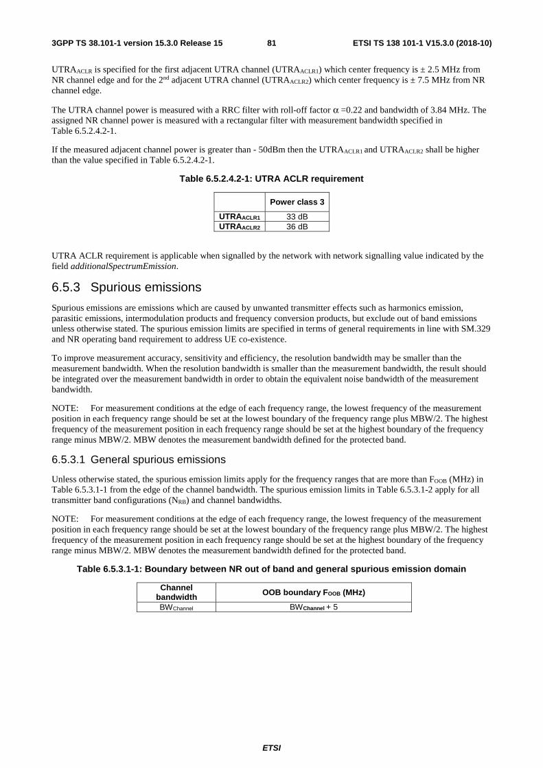
ETSI
ETSI TS 138 101-1 V15.3.0 (2018-10)813GPP TS 38.101-1 version 15.3.0 Release 15
UTRAACLR is specified for the first adjacent UTRA channel (UTRAACLR1) which center frequency is ± 2.5 MHz from NR channel edge and for the 2nd adjacent UTRA channel (UTRAACLR2) which center frequency is ± 7.5 MHz from NR channel edge.
The UTRA channel power is measured with a RRC filter with roll-off factor α =0.22 and bandwidth of 3.84 MHz. The assigned NR channel power is measured with a rectangular filter with measurement bandwidth specified in Table 6.5.2.4.2-1.
If the measured adjacent channel power is greater than - 50dBm then the UTRAACLR1 and UTRAACLR2 shall be higher than the value specified in Table 6.5.2.4.2-1.
Table 6.5.2.4.2-1: UTRA ACLR requirement
Power class 3
UTRAACLR1 33 dB UTRAACLR2 36 dB
UTRA ACLR requirement is applicable when signalled by the network with network signalling value indicated by the field additionalSpectrumEmission.
6.5.3 Spurious emissions
Spurious emissions are emissions which are caused by unwanted transmitter effects such as harmonics emission, parasitic emissions, intermodulation products and frequency conversion products, but exclude out of band emissions unless otherwise stated. The spurious emission limits are specified in terms of general requirements in line with SM.329 and NR operating band requirement to address UE co-existence.
To improve measurement accuracy, sensitivity and efficiency, the resolution bandwidth may be smaller than the measurement bandwidth. When the resolution bandwidth is smaller than the measurement bandwidth, the result should be integrated over the measurement bandwidth in order to obtain the equivalent noise bandwidth of the measurement bandwidth.
NOTE: For measurement conditions at the edge of each frequency range, the lowest frequency of the measurement position in each frequency range should be set at the lowest boundary of the frequency range plus MBW/2. The highest frequency of the measurement position in each frequency range should be set at the highest boundary of the frequency range minus MBW/2. MBW denotes the measurement bandwidth defined for the protected band.
6.5.3.1 General spurious emissions
Unless otherwise stated, the spurious emission limits apply for the frequency ranges that are more than FOOB (MHz) in Table 6.5.3.1-1 from the edge of the channel bandwidth. The spurious emission limits in Table 6.5.3.1-2 apply for all transmitter band configurations (NRB) and channel bandwidths.
NOTE: For measurement conditions at the edge of each frequency range, the lowest frequency of the measurement position in each frequency range should be set at the lowest boundary of the frequency range plus MBW/2. The highest frequency of the measurement position in each frequency range should be set at the highest boundary of the frequency range minus MBW/2. MBW denotes the measurement bandwidth defined for the protected band.
Table 6.5.3.1-1: Boundary between NR out of band and general spurious emission domain
Channel bandwidth OOB boundary FOOB (MHz)
BWChannel BWChannel + 5

ETSI
ETSI TS 138 101-1 V15.3.0 (2018-10)823GPP TS 38.101-1 version 15.3.0 Release 15
Table 6.5.3.1-2: Requirement for general spurious emissions limits
Frequency Range Maximum Level
Measurement bandwidth
NOTE
9 kHz ≤ f < 150 kHz -36 dBm 1 kHz 150 kHz ≤ f < 30 MHz -36 dBm 10 kHz
30 MHz ≤ f < 1000 MHz -36 dBm 100 kHz 1 GHz ≤ f < 12.75 GHz -30 dBm 1 MHz
-25 dBm 1 MHz 12.75 GHz ≤ f < 5th
harmonic of the upper frequency edge of the UL operating band in
GHz
-30 dBm 1 MHz 1
12.75 GHz < f < 26 GHz -30 dBm 1 MHz 2 NOTE 1: Applies for Band that the upper frequency edge of the UL Band more
than 2.69 GHz NOTE 2: Applies for Band that the upper frequency edge of the UL Band more
than 5.2 GHz NOTE 3: Applies for EN-DC combinations that include n41 when NS_04 is
signalled.
6.5.3.2 Spurious emissions for UE co-existence
This clause specifies the requirements for NR bands for coexistence with protected bands.

ETSI
ETSI TS 138 101-1 V15.3.0 (2018-10)833GPP TS 38.101-1 version 15.3.0 Release 15
Table 6.5.3.2-1: Requirements for spurious emissions for UE co-existence

ETSI
ETSI TS 138 101-1 V15.3.0 (2018-10)843GPP TS 38.101-1 version 15.3.0 Release 15
NR Band
Spurious emission for UE co-existence
Protected band Frequency range (MHz) Maximum Level (dBm)
MBW (MHz)
NOTE
n1, n84 E-UTRA Band 1, 5, 7, 8, 11, 18, 19, 20, 21, 22, 26, 27, 28, 31, 32, 38, 40, 41, 42, 43, 44, 45, 50, 51, 65, 67, 68, 69, 72, 73,
74, 75, 76, NR Band n78, n79
FDL_low - FDL_high -50 1
NR Band n77 FDL_low - FDL_high -50 1 2 E-UTRA Band 3, 34 FDL_low - FDL_high -50 1 15
Frequency range 1880 - 1895 -40 1 15, 27
Frequency range 1895 - 1915 -15.5 5 15, 26, 27
Frequency range 1915 - 1920 +1.6 5 15, 26, 27
n2
E-UTRA Band 4, 5, 10, 12, 13, 14, 17, 24, 26, 27, 28, 29, 30,
41, 42, 48, 50, 51, 66, 70, 71, 74
FDL_low - FDL_high -50 1
E-UTRA Band 2, 25 FDL_low - FDL_high -50 1 15 E-UTRA Band 43 FDL_low - FDL_high -50 1 2
n3, n80
E-UTRA Band 1, 5, 7, 8, 20, 26, 27, 28, 31, 32, 33, 34, 38, 39, 40, 41, 43, 44, 45, 50, 51, 65, 67, 68, 69, 72, 73,74, 75, 76.
NR Band n79
FDL_low - FDL_high -50 1
E-UTRA Band 3 FDL_low - FDL_high -50 1 15 E-UTRA Band 11, 18, 19, 21 FDL_low - FDL_high -50 1 13
E-UTRA Band 22, 42, NR Band n77, n78
FDL_low - FDL_high -50 1 2
Frequency range 1884.5 - 1915.7 -41 0.3 13 n5 E-UTRA Band 1, 2, 3, 4, 5, 7, 8,
10, 12, 13, 14, 17, 18, 19, 24, 25, 26, 28, 29, 30, 31, 34, 38, 40, 42, 43, 45, 48, 50, 51, 65,
66, 70, 71, 73, 74, 85
FDL_low - FDL_high -50
E-UTRA Band 41, 52 FDL_low - FDL_high -50 1 2 E-UTRA Band 11, 21 FDL_low - FDL_high -50 1 39
Frequency range 1884.5 - 1915.7 -41 0.3 8,39 n7
E-UTRA Band 1, 2, 3, 4, 5, 7, 8, 10, 12, 13, 14, 17, 20, 22, 26, 27, 28, 29, 30, 31, 32, 33, 34, 40, 42, 43, 50, 51, 65, 66, 67,
68, 72, 74, 75, 76, NR Band n77, n78
FDL_low - FDL_high -50 1
Frequency range 2570 - 2575 +1.6 5 15, 21, 26
Frequency range 2575 - 2595 -15.5 5 15, 21, 26
Frequency range 2595 - 2620 -40 1 15, 21 n8, n81
E-UTRA Band 1, 20, 28, 31, 32, 33, 34, 38, 39, 40, 45, 50, 51,
65, 67, 68, 69, 72, 73, 74, 75, 76
FDL_low - FDL_high -50 1
E-UTRA band 3, 7, 22, 41, 42, 43,
NR Band n77, n78, n79
FDL_low - FDL_high -50 1 2
E-UTRA 8 FDL_low - FDL_high -50 1 15 E-UTRA Band 11, 21 FDL_low - FDL_high -50 1
Frequency range 1884.5 - 1915.7 -41 0.3 8 n12 E-UTRA Band 2, 5, 13, 14, 17,
24, 25, 26, 27, 30, 41, 48, 50, 51, 71, 74
FDL_low
- FDL_high
-50 1
E-UTRA Band 4, 10, 66, 70 FDL_low
- FDL_high
-50 1 2

ETSI
ETSI TS 138 101-1 V15.3.0 (2018-10)853GPP TS 38.101-1 version 15.3.0 Release 15
NR Band
Spurious emission for UE co-existence
Protected band Frequency range (MHz) Maximum Level (dBm)
MBW (MHz)
NOTE
E-UTRA Band 12, 85 FDL_low
- FDL_high
-50 1 15
n20, n82
E-UTRA Band 1, 3, 7, 8, 22, 31, 32, 33, 34, 40, 43, 50, 51, 65,
67, 68, 72, 74, 75, 76
FDL_low - FDL_high -50 1
E-UTRA Band 20 FDL_low - FDL_high -50 1 15 E-UTRA Band 38, 42, 69,
NR Band n77, n78 FDL_low - FDL_high -50 1 2
Frequency range 758 - 788 -50 1 n25 E-UTRA Band 4, 5, 10,12, 13,
14, 17, 24, 26, 27, 28, 29, 30, 41, 42, 48, 66, 70, 71, 85
FDL_low - FDL_high -50 1
E-UTRA Band 2 FDL_low - FDL_high -50 1 15 E-UTRA Band 25 FDL_low - FDL_high -50 1 15 E-UTRA Band 43 FDL_low - FDL_high -50 1 2
n28, n83
E-UTRA Band 1, 4, 10, 22, 42, 43, 50, 51, 65, 73, 74, 75, 76,
NR Band n77, n78
FDL_low - FDL_high -50 1 2
E-UTRA Band 1 FDL_low - FDL_high -50 1 19, 25 E-UTRA Band 2, 3, 5, 7, 8, 18, 19, 20, 25, 26, 27, 31, 34, 38,
40, 41, 66, 72, NR Band n79
FDL_low - FDL_high -50 1
E-UTRA Band 11, 21 FDL_low - FDL_high -50 1 19, 24 Frequency range 470 - 694 -42 8 15, 35 Frequency range 470 - 710 -26.2 6 34 Frequency range 662 - 694 -26.2 6 15 Frequency range 758 - 773 -32 1 15 Frequency range 773 - 803 -50 1 Frequency range 1884.5 - 1915.7 -41 0.3 8, 19
n34 E-UTRA Band 1, 3, 7, 8, 11, 18, 19, 20, 21, 22, 26, 28, 31, 32,
33, 38,39, 40, 41, 42, 43, 44, 45, 50, 51, 65, 67, 69, 72, 74, 75,
76, NR Band n78, n79
FDL_low - FDL_high -50 1 5
NR Band n77 FDL_low - FDL_high -50 1 2 Frequency range 1884.5 - 1915.7 -41 0.3 8
n38
E-UTRA Band 1, 2, 3, 4, 5, 8, 10, 12, 13, 14, 17, 20, 22, 27, 28, 29, 30, 31, 32, 33, 34, 40, 42, 43, 50, 51, 65, 66, 67, 68,
72, 74, 75, 76
FDL_low - FDL_high -50 1
Frequency range 2620 - 2645 -15.5 5 15, 22, 26
Frequency range 2645 - 2690 -40 1 15, 22 n39 E-UTRA Band 1, 8, 22, 26, 34,
40, 41, 42, 44, 45, 50, 51, 74, NR Band n79
FDL_low - FDL_high -50 1
NR Band n77, n78 FDL_low - FDL_high -50 1 2 Frequency range 1805 - 1855 -40 1 33 Frequency range 1855 - 1880 -15.5 5 15, 26,
33 n40 E-UTRA Band 1, 3, 5, 7, 8, 20,
22, 26, 27, 28, 31, 32, 33, 34, 38, 39, 41, 42, 43, 44, 45, 50, 51, 65, 67, 68, 69, 72, 74, 75,
76, NR Band n77, n78
FDL_low - FDL_high -50 1
NR Band n79 FDL_low - FDL_high -50 1 2

ETSI
ETSI TS 138 101-1 V15.3.0 (2018-10)863GPP TS 38.101-1 version 15.3.0 Release 15
NR Band
Spurious emission for UE co-existence
Protected band Frequency range (MHz) Maximum Level (dBm)
MBW (MHz)
NOTE
n41
E-UTRA Band 1, 2, 3, 4, 5, 8, 10, 12, 13, 14, 17, 24, 25, 26, 27, 28, 29, 30, 34, 39, 40, 42, 44, 45, 48, 50, 51, 65, 66, 70,
71, 73, 74, NR Band n77, n78
FDL_low - FDL_high -50 1
NR Band n79 FDL_low - FDL_high -50 1 2 E-UTRA Band 9, 11, 18, 19, 21 FDL_low - FDL_high -50 1 30
Frequency range 1884.5 1915.7 -41 0.3 8, 30 n50 E-UTRA Band 1, 2, 3, 4, 5, 7, 8,
12, 13, 17, 20, 26, 28, 29, 31, 34, 38, 39, 40, 41, 42, 43, 48,
65, 66, 67, 68
FDL_low - FDL_high -50 1
n51 E-UTRA Band 1, 2, 3, 4, 5, 7, 8, 12, 13, 17, 20, 26, 28, 29, 31, 34, 38, 39, 40, 41, 42, 43, 48,
65, 66, 67, 68
FDL_low - FDL_high -50 1
n66, n86
E-UTRA Band 1, 2, 3, 4, 5, 7, 8, 12, 13, 17, 20, 26, 28, 29, 31, 34, 38, 39, 40, 41, 42, 43, 48,
65, 66, 67, 68, 70, 71
FDL_low - FDL_high -50 1
E-UTRA Band 42, 48 FDL_low - FDL_high -50 1 2 n70 E-UTRA Band 2, 4, 5, 10, 12,
13, 14, 17, 24, 25, 29, 30, 41, 48, 66, 70, 71
FDL_low - FDL_high -50 1 2
n71
E-UTRA Band 4, 5, 12, 13, 14, 17, 24, 26, 30, 48, 66, 85
FDL_low - FDL_high -50 1
E-UTRA Band 2, 25, 41, 70 FDL_low - FDL_high -50 1 2 E-UTRA Band 29 FDL_low - FDL_high -38 1 15 E-UTRA Band 71 FDL_low - FDL_high -50 1 15
n74
E-UTRA Band 1, 2, 3, 4, 5, 7, 8, 12, 13, 17, 18, 19, 20, 26, 28, 29, 31, 34, 38, 39, 40, 41, 42,
43, 48, 65, 66, 67, 68
FDL_low - FDL_high -50 1
Frequency range 1884.5 - 1915.7 -41 0.3 8 Frequency range 1400 - 1427 -32 27 15, 41 Frequency range 1475 - 1488 -50 1 42 Frequency range 1488 - 1518 -50 1 15
n77, n78 E-UTRA Band 1, 3, 5, 7, 8, 11, 18, 19, 20, 21, 26, 28, 34, 39,
40, 41, 65
FDL_low - FDL_high -50 1
Frequency range 1884.5 - 1915.7 -41 0.3 8 NR Band n257 26500 - 29500 -5 100
n79 E-UTRA Band 1, 3, 5, 8, 11, 18, 19, 21, 28, 34, 39, 40, 41, 42, 65
FDL_low - FDL_high -50 1
Frequency range 1884.5 - 1915.7 -41 0.3 8 NR Band n257 26500 - 29500 -5 100
n80 See n3 n81 See n8 n82 See n20 n83 See n28 n84 See n1 n86 See n66

ETSI
ETSI TS 138 101-1 V15.3.0 (2018-10)873GPP TS 38.101-1 version 15.3.0 Release 15
NOTE 1: FDL_low and FDL_high refer to each frequency band specified in Table 5.2-1 or Table 5.5-1 in TS 36.101
NOTE 2: As exceptions, measurements with a level up to the applicable requirements defined in Table 6.5.3.1-2 are permitted for each assigned NR carrier used in the measurement due to 2nd, 3rd, 4th or 5th harmonic spurious emissions. Due to spreading of the harmonic emission the exception is also allowed for the first 1 MHz frequency range immediately outside the harmonic emission on both sides of the harmonic emission. This results in an overall exception interval centred at the harmonic emission of (2MHz + N x LCRB x 180kHz), where N is 2, 3, 4, 5 for the 2nd, 3rd, 4th or 5th harmonic respectively. The exception is allowed if the measurement bandwidth (MBW) totally or partially overlaps the overall exception interval.
NOTE 3: 15 kHz SCS is assumed when RB is mentioned in the note. NOTE 4: N/A NOTE 5: For non-synchronised TDD operation to meet these requirements some restriction will be needed
for either the operating band or protected band NOTE 6: N/A NOTE 7: Applicable when co-existence with PHS system operating in 1884.5 - 1919.6 MHz. NOTE 8: Applicable when co-existence with PHS system operating in 1884.5 - 1915.7 MHz. NOTE 9: N/A NOTE 10: N/A NOTE 11: Whether the applicable frequency range should be 793-805MHz instead of 799-805MHz is TBD NOTE 12: The emissions measurement shall be sufficiently power averaged to ensure a standard deviation <
0.5 dB NOTE 13: This requirement applies for 5, 10, 15 and 20 MHz NR channel bandwidth allocated within
1744.9MHz and 1784.9MHz. NOTE 14: N/A NOTE 15: These requirements also apply for the frequency ranges that are less than FOOB (MHz) in Table
6.5.3.1-1 and Table 6.5A.3.1-1 from the edge of the channel bandwidth. NOTE 16: N/A NOTE 17: N/A NOTE 18: N/A NOTE 19: Applicable when the assigned NR carrier is confined within 718 MHz and 748 MHz and when the
channel bandwidth used is 5 or 10 MHz. NOTE 20: N/A NOTE 21: This requirement is applicable for any channel bandwidths within the range 2500 - 2570 MHz with
the following restriction: for carriers of 15 MHz bandwidth when carrier centre frequency is within the range 2560.5 - 2562.5 MHz and for carriers of 20 MHz bandwidth when carrier centre frequency is within the range 2552 - 2560 MHz the requirement is applicable only for an uplink transmission bandwidth less than or equal to 54 RB.
NOTE 22: This requirement is applicable for power class 3 UE for any channel bandwidths within the range 2570 - 2615 MHz with the following restriction: for carriers of 15 MHz bandwidth when carrier centre frequency is within the range 2605.5 - 2607.5 MHz and for carriers of 20 MHz bandwidth when carrier centre frequency is within the range 2597 - 2605 MHz the requirement is applicable only for an uplink transmission bandwidth less than or equal to 54 RB. For power class 2 UE for any channel bandwidths within the range 2570 - 2615 MHz, NS_44 shall apply. For power class 2 or 3 UE for carriers with channel bandwidth overlapping the frequency range 2615 - 2620 MHz the requirement applies with the maximum output power configured to +19 dBm in the IE P-Max.
NOTE 23: Void NOTE 24: As exceptions, measurements with a level up to the applicable requirement of -38 dBm/MHz is
permitted for each assigned NR carrier used in the measurement due to 2nd harmonic spurious emissions. An exception is allowed if there is at least one individual RB within the transmission bandwidth (see Figure 5.3.3-1) for which the 2nd harmonic totally or partially overlaps the measurement bandwidth (MBW).
NOTE 25: As exceptions, measurements with a level up to the applicable requirement of -36 dBm/MHz is permitted for each assigned NR carrier used in the measurement due to 3rd harmonic spurious emissions. An exception is allowed if there is at least one individual RB within the transmission bandwidth (see Figure 5.3.3-1) for which the 3rd harmonic totally or partially overlaps the measurement bandwidth (MBW).
NOTE 26: For these adjacent bands, the emission limit could imply risk of harmful interference to UE(s) operating in the protected operating band.
NOTE 27: This requirement is applicable for any channel bandwidths within the range 1920 - 1980 MHz with the following restriction: for carriers of 15 MHz bandwidth when carrier centre frequency is within the range 1927.5 - 1929.5 MHz and for carriers of 20 MHz bandwidth when carrier centre frequency is within the range 1930 - 1938 MHz the requirement is applicable only for an uplink transmission bandwidth less than or equal to 54 RB.
NOTE 28: N/A NOTE 29: N/A NOTE 30: This requirement applies when the NR carrier is confined within 2545-2575MHz or 2595-2645MHz
and the channel bandwidth is 10 or 20 MHz

ETSI
ETSI TS 138 101-1 V15.3.0 (2018-10)883GPP TS 38.101-1 version 15.3.0 Release 15
NR Band
Spurious emission for UE co-existence
Protected band Frequency range (MHz) Maximum Level (dBm)
MBW (MHz)
NOTE
NOTE 31: N/A NOTE 32: Void NOTE 33: This requirement is only applicable for carriers with bandwidth confined within 1885-1920 MHz
(requirement for carriers with at least 1RB confined within 1880 - 1885 MHz is not specified). This requirement applies for an uplink transmission bandwidth less than or equal to 54 RB for carriers of 15 MHz bandwidth when carrier center frequency is within the range 1892.5 - 1894.5 MHz and for carriers of 20 MHz bandwidth when carrier center frequency is within the range 1895 - 1903 MHz.
NOTE 34: This requirement is applicable for 5 and 10 MHz NR channel bandwidth allocated within 718-728MHz. For carriers of 10 MHz bandwidth, this requirement applies for an uplink transmission bandwidth less than or equal to 30 RB with RBstart > 1 and RBstart<48.
NOTE 35: This requirement is applicable in the case of a 10 MHz NR carrier confined within 703 MHz and 733 MHz, otherwise the requirement of -25 dBm with a measurement bandwidth of 8 MHz applies.
NOTE 36: This requirement is applicable for NR channel bandwidth allocated within 1920-1980 MHz. NOTE 37: Applicable when the upper edge of the channel bandwidth frequency is greater than 1980MHz. NOTE 38: Applicable when NS_33 or NS_34 is configured by the pre-configured radio parameters. NOTE 39: Void. NOTE 40: In the frequency range x-5950MHz, SE requirement of -30dBm/MHz should be applied; where x =
max (5925, fc + 15), where fc is the channel centre frequency. NOTE 41: Applicable for 1.4 MHz bandwidth, and when the lower edge of the assigned NR UL channel
bandwidth frequency is greater than or equal to 1427 MHz + the channel BW assigned for 3, 5 and 10 MHz bandwidth, and when the lower edge of the assigned E-UTRA UL channel bandwidth frequency is greater than or equal to 1440 MHz for 15 and 20 MHz bandwidth.
NOTE 42: Applicable for 1.4 , 3 and 5 MHz bandwidth, and when the upper edge of the assigned NR UL channel bandwidth frequency is less than or equal to 1467 MHz assigned for10 MHz bandwidth, and when the upper edge of the assigned NR UL channel bandwidth frequency is less than or equal to 1463.8 MHz for 15 MHz bandwidth, and when the upper edge of the assigned NR UL channel bandwidth frequency is less than or equal to 1460.8 MHz for 20 MHz bandwidth.
NOTE: To simplify Table 6.5.3.2-1, E-UTRA band numbers are listed for bands which are specified only for E-UTRA operation or both E-UTRA and NR operation. NR band numbers are listed for bands which are specified only for NR operation.
6.5.3.3 Additional spurious emissions
These requirements are specified in terms of an additional spectrum emission requirement. Additional spurious emission requirements are signalled by the network to indicate that the UE shall meet an additional requirement for a specific deployment scenario as part of the cell handover/broadcast message.
NOTE: For measurement conditions at the edge of each frequency range, the lowest frequency of the measurement position in each frequency range should be set at the lowest boundary of the frequency range plus MBW/2. The highest frequency of the measurement position in each frequency range should be set at the highest boundary of the frequency range minus MBW/2. MBW denotes the measurement bandwidth defined for the protected band.
6.5.3.3.1 Requirement for network signalled value "NS_04"
When "NS 04" is indicated in the cell, the power of any UE emission shall not exceed the levels specified in Table 6.6.3.3.1-1. This requirement also applies for the frequency ranges that are less than FOOB (MHz) in Table 6.5.3.1-1 from the edge of the channel bandwidth.
Table 6.5.3.3.1-1: Additional requirements
Frequency range (MHz)
Channel bandwidth / Spectrum emission limit (dBm)
Measurement bandwidth
10, 15, 20, 40, 50, 60, 80, 90, 100 MHz
2495 ≤ f < 2496 -13 1% of Channel BW 2490.5 ≤ f < 2495 -13 1 MHz
0 < f < 2490.5 -25 1 MHz

ETSI
ETSI TS 138 101-1 V15.3.0 (2018-10)893GPP TS 38.101-1 version 15.3.0 Release 15
6.5.3.3.2 Requirement for network signalled value “NS_17”
When “NS_17” is indicated in the cell, the power of any UE emission shall not exceed the levels specified in Table 6.5.3.3.2-1. This requirement also applies for the frequency ranges that are less than FOOB (MHz) in Table 6.5.3.1-1 from the edge of the channel bandwidth.
Table 6.5.3.3.2-1: Additional requirements
Frequency range (MHz)
Channel bandwidth / Spectrum emission limit (dBm)
Measurement bandwidth
NOTE
5, 10 MHz
470 ≤ f ≤ 710 -26.2 6 MHz 1 NOTE 1: Applicable when the assigned E-UTRA carrier is confined within 718 MHz and 748 MHz and when the channel bandwidth used is 5 or 10 MHz.
6.5.3.3.3 Requirement for network signalled value “NS_18”
When “NS_18” is indicated in the cell, the power of any UE emission shall not exceed the levels specified in Table 6.5.3.3. 3-1. This requirement also applies for the frequency ranges that are less than FOOB (MHz) in Table 6.5.3.1-1 from the edge of the channel bandwidth.
Table 6.5.3.3.3-1: Additional requirements
Frequency range (MHz)
Channel bandwidth / Spectrum emission limit (dBm)
Measurement bandwidth
NOTE
5, 10, 15, 20 MHz
692-698 -26.2 6 MHz
6.5.3.3.4 Requirement for network signalled value “NS_05”
When “NS_05” is indicated in the cell, the power of any UE emission shall not exceed the levels specified in Table 6.5.3.3.4-1. This requirement also applies for the frequency ranges that are less than FOOB (MHz) in Table 6.5.3.1-1 from the edge of the channel bandwidth.
Table 6.5.3.3.4-1: Additional requirements
Frequency band (MHz)
Channel bandwidth / Spectrum emission limit (dBm)
Measurement bandwidth
NOTE
5MHz 10MHz 15MHz 20MHz 1884.5 ≤ f ≤1915.7 -41 -41 -41 -41 300 KHz
6.5.3.3.5 Requirement for network signalled value “NS_08”
When “NS08” is indicated in the cell, the power of any UE emission shall not exceed the levels specified in Table 6.5.3.3.5-1. This requirement also applies for the frequency ranges that are less than FOOB (MHz) in Table 6.5.3.1-1 from the edge of the channel bandwidth.
Table 6.5.3.3.5-1: Additional requirement
Frequency range (MHz)
Channel bandwidth / Spectrum emission limit (dBm) Measurement bandwidth
5 MHz 10 MHz 15 MHz
860 ≤ f ≤ 890 -40 -40 -40 1 MHz
6.5.3.3.6 Requirement for network signalled value “NS_37”
When “NS 37” is indicated in the cell, the power of any UE emission shall not exceed the levels specified in Table 6.5.3.3.6-1. This requirement also applies for the frequency ranges that are less than FOOB (MHz) in Table 6.5.3.1-1 from the edge of the channel bandwidth.

ETSI
ETSI TS 138 101-1 V15.3.0 (2018-10)903GPP TS 38.101-1 version 15.3.0 Release 15
Table 6.5.3.3.6-1: Additional requirement
Frequency band (MHz)
Channel bandwidth / Spectrum emission limit (dBm) Measurement bandwidth
5MHz 10MHz 15MHz 20MHz
1475.9 ≤ f ≤ 1510.9 -35 -35 -35 -35 1 MHz
6.5.3.3.7 Requirement for network signalled value “NS_38”
When “NS 38” is indicated in the cell, the power of any UE emission shall not exceed the levels specified in Table 6.5.3.3.7-1. This requirement also applies for the frequency ranges that are less than FOOB (MHz) in Table 6.5.3.1-1 from the edge of the channel bandwidth.
Table 6.5.3.3.7-1: Additional requirements
Frequency band (MHz)
Channel bandwidth / Spectrum emission limit
(dBm)
Measurement bandwidth
5 MHz, 10 MHz, 15 MHz, 20 MHz 1400 ≤ f ≤ 1427 -32 27MHz
NOTE 1: This requirement shall be verified with UE transmission power of 15 dBm.
6.5.3.3.8 Requirement for network signalled value “NS_39”
When “NS 39” is indicated in the cell, the power of any UE emission shall not exceed the levels specified in Table 6.5.3.3.8-1. This requirement also applies for the frequency ranges that are less than FOOB (MHz) in Table 6.5.3.1-1 from the edge of the channel bandwidth.
Table 6.5.3.3.8-1: Additional requirements
Frequency band (MHz)
Channel bandwidth / Spectrum emission limit
(dBm)
Measurement bandwidth
5 MHz, 10 MHz, 15 MHz, 20 MHz 1475 ≤ f ≤ 1488 -28 1MHz
6.5.4 Transmit intermodulation
The transmit intermodulation performance is a measure of the capability of the transmitter to inhibit the generation of signals in its non linear elements caused by presence of the wanted signal and an interfering signal reaching the transmitter via the antenna.
UE transmit intermodulation is defined by the ratio of the mean power of the wanted signal to the mean power of the intermodulation product when an interfering CW signal is added at a level below the wanted signal at each transmitter antenna port with the other antenna port(s) if any terminated. Both the wanted signal power and the intermodulation product power are measured through NR rectangular filter with measurement bandwidth shown in Table 6.5.4-1.
The requirement of transmit intermodulation is specified in Table 6.5.4-1.

ETSI
ETSI TS 138 101-1 V15.3.0 (2018-10)913GPP TS 38.101-1 version 15.3.0 Release 15
Table 6.5.4-1: Transmit Intermodulation
Wanted signal channel bandwidth BWChannel
Interference signal frequency offset from channel center
BWChannel 2*BWChannel
Interference CW signal level -40dBc
Intermodulation product < -29dBc < -35dBc
Measurement bandwidth The maximum transmission bandwidth configuration among the different SCSs for the channel BW as defined in Table 6.5.2.1.1-1
Measurement offset from channel center BWChannel and 2*BWChannel 2*BWChannel and 4*BWChannel
6.5A Output RF spectrum emissions for CA For inter-band carrier aggregation with one uplink carrier assigned to one NR band, the output RF spectrum emissions requirements in subclause 6.5 apply.
6.5A.1 Occupied bandwidth for CA
6.5A.1.1 Occupied bandwidth for Intra-band contiguous CA
6.5A.1.2 Occupied bandwidth for Intra-band non-contiguous CA
6.5A.1.3 Occupied bandwidth for Inter-band CA
For inter-band carrier aggregation with uplink assigned to two NR bands, the occupied bandwidth is defined per component carrier. Occupied bandwidth is the bandwidth containing 99 % of the total integrated mean power of the transmitted spectrum on assigned channel bandwidth on the component carrier. The occupied bandwidth shall be less than the channel bandwidth specified in Table 6.5.1-1.
6.5A.2 Out of band emission for CA
6.5A.2.1 General
Detailed structure of the subclause is TBD
6.5A.2.2 Spectrum emission mask
6.5A.2.2.1 Spectrum emission mask for Intra-band contiguous CA
6.5A.2.2.2 Spectrum emission mask for Intra-band non-contiguous CA
6.5A.2.2.3 Spectrum emission mask for Inter-band CA
For inter-band carrier aggregation with uplink assigned to two NR bands, the spectrum emission mask of the UE is defined per component carrier while both component carriers are active and the requirements are specified in subclauses 6.5.2.1 and 6.5.2.2. If for some frequency spectrum emission masks of component carriers overlap then spectrum emission mask allowing higher power spectral density applies for that frequency. If for some frequency a component carrier spectrum emission mask overlaps with the channel bandwidth of another component carrier, then the emission mask does not apply for that frequency.

ETSI
ETSI TS 138 101-1 V15.3.0 (2018-10)923GPP TS 38.101-1 version 15.3.0 Release 15
6.5A.2.3 Additional spectrum emission mask
6.5A.2.3.1 Additional spectrum emission mask for Intra-band contiguous CA
6.5A.2.3.2 Additional spectrum emission mask for Intra-band non-contiguous CA
6.5A.2.3.3 Additional spectrum emission mask for Inter-band CA
6.5A.2.4 Adjacent channel leakage ratio
6.5A.2.4.1 NR ACLR
6.5A.2.4.1.1 NR ACLR for Intra-band contiguous CA
6.5A.2.4.1.2 NR ACLR for Intra-band non-contiguous CA
6.5A.2.4.1.3 NR ACLR for Inter-band CA
For inter-band carrier aggregation with uplink assigned to two NR bands, the NR Adjacent Channel Leakage power Ratio (NRACLR) is defined per component carrier while both component carriers are active and the requirement is specified in subclause 6.5.2.4.1.
6.5A.2.4.2 UTRA ACLR
6.5A.2.4.2.1 UTRA ACLR for Intra-band contiguous CA
6.5A.2.4.2.2 UTRA ACLR for Intra-band non-contiguous CA
6.5A.2.4.2.3 UTRA ACLR for Inter-band CA
For inter-band carrier aggregation with uplink assigned to two NR bands, the UTRA Adjacent Channel Leakage power Ratio (UTRAACLR) is defined per component carrier while both component carrier are active and the requirement is specified in subclause 6.5.2.4.2.
6.5A.3 Spurious emission for CA
6.5A.3.1 General spurious emissions
For inter-band carrier aggregation with uplink assigned to two NR bands, the spurious emission requirement Table 6.5.3.1-2 apply for the frequency ranges that are more than FOOB as defined in Table 6.5.3.1-1 away from edges of the assigned channel bandwidth on a component carrier. If for some frequency a spurious emission requirement of individual component carrier overlaps with the spectrum emission mask or channel bandwidth of another component carrier then it does not apply.
6.5A.3.2 Spurious emissions for UE co-existence
6.5A.3.2.1 Spurious emissions for UE co-existence for Intra-band contiguous CA
6.5A.3.2.2 Spurious emissions for UE co-existence for Intra-band non-contiguous CA
6.5A.3.2.3 Spurious emissions for UE co-existence for Inter-band CA
For inter-band carrier aggregation with the uplink assigned to two NR bands, the requirements in Table 6.5A.3.2-1 apply on each component carrier with all component carriers are active.
NOTE: For inter-band carrier aggregation with uplink assigned to two NR bands the requirements in Table 6.5A.3.2-1 could be verified by measuring spurious emissions at the specific frequencies where second and third order intermodulation products generated by the two transmitted carriers can occur; in that case, the requirements for remaining applicable frequencies in Table 6.5A.3.2-1 would be considered to be verified by the measurements verifying the one uplink inter-band CA UE to UE co-existence requirements.

ETSI
ETSI TS 138 101-1 V15.3.0 (2018-10)933GPP TS 38.101-1 version 15.3.0 Release 15
Table 6.5A.3.2.3-1: Requirements for uplink inter-band carrier aggregation (two bands)
NR CA Configuration
Spurious emission Protected Band Frequency range (Mhz) Maximum
Level (dBm)
MBW (MHz)
NOTE
CA_n3A-n78A E-UTRA Band 1, 3, 5, 7, 8, 11, 18, 19, 20, 21, 26, 28, 34, 39,
40, 41, 65 FDL_low - FDL_high -50 1
Frequency range 1884.5 - 1915.7 -41 0.3 3 NR Band n257 26500 - 29500 -5 100
CA_n8A-n78A E-UTRA Band 1,8, 20, 28, 34, 39, 40,65 FDL_low - FDL_high -50 1
E-UTRA Band 3, 7,41 FDL_low - FDL_high -50 1 2 E-UTRA Band 11, 21 FDL_low - FDL_high -50 1 5
Frequency range 860 - 890 -40 1 4,5 Frequency range 1884.5 - 1915.7 -41 0.3 3 NR Band n257 26500 - 29500 -5 100 NR Band n258 24250 - 27500 -5 100
NOTE 1: FDL_low and FDL_high refer to each frequency band specified in Table 5.2-1 or Table 5.5-1 in TS 36.101 NOTE 2: As exceptions, measurements with a level up to the applicable requirements defined in Table 6.5.3.1-2 are
permitted for each assigned NR carrier used in the measurement due to 2nd, 3rd, 4th or 5th harmonic spurious emissions. Due to spreading of the harmonic emission the exception is also allowed for the first 1 MHz frequency range immediately outside the harmonic emission on both sides of the harmonic emission. This results in an overall exception interval centred at the harmonic emission of (2MHz + N x LCRB x 180kHz), where N is 2, 3, 4, 5 for the 2nd, 3rd, 4th or 5th harmonic respectively. The exception is allowed if the measurement bandwidth (MBW) totally or partially overlaps the overall exception interval.
NOTE 3: Applicable when co-existence with PHS system operating in 1884.5 -1915.7MHz NOTE 4: These requirements also apply for the frequency ranges that are less than FOOB (MHz) in Table 6.5.3.1-1
and Table 6.5A.3.1-1 from the edge of the channel bandwidth. NOTE 5: This requirement is applicable only for the following cases: - for carriers of 5 MHz channel bandwidth when
carrier centre frequency (Fc) is within the range 902.5 MHz ≤ Fc < 907.5 MHz with an uplink transmission bandwidth less than or equal to 20 RB - for carriers of 5 MHz channel bandwidth when carrier centre frequency (Fc) is within the range 907.5 MHz ≤ Fc ≤ 912.5 MHz without any restriction on uplink transmission bandwidth. - for carriers of 10 MHz channel bandwidth when carrier centre frequency (Fc) is Fc = 910 MHz with an uplink transmission bandwidth less than or equal to 32 RB with RBstart > 3.
NOTE: To simplify Table 6.5A.3.2.3-1, E-UTRA band numbers are listed for bands which are specified only for E-UTRA operation or both E-UTRA and NR operation. NR band numbers are listed for bands which are specified only for NR operation.
6.5A.4 Transmit intermodulation for CA
6.5A.3.2.1 Transmit intermodulation for Intra-band contiguous CA
6.5A.3.2.2 Transmit intermodulation for Intra-band non-contiguous CA
6.5A.3.2.3 Transmit intermodulation for Inter-band CA
For inter-band carrier aggregation with uplink assigned to two NR bands, the transmit intermodulation requirement is specified in Table 6.5.4-1 which shall apply on each component carrier with both component carriers active.
6.5D Output RF spectrum emissions for UL-MIMO
6.5D.1 Occupied bandwidth for UL-MIMO
For UE supporting UL-MIMO, the requirements for occupied bandwidth is specified at each transmit antenna connector. The occupied bandwidth is defined as the bandwidth containing 99 % of the total integrated mean power of the transmitted spectrum on the assigned channel at each transmit antenna connector.
For UE with two transmit antenna connectors in closed-loop spatial multiplexing scheme, the occupied bandwidth at each transmitter antenna shall be less than the channel bandwidth specified in table 6.5.1-1. The requirements shall be met with UL-MIMO configurations described in sub-clause 6.2D.1.

ETSI
ETSI TS 138 101-1 V15.3.0 (2018-10)943GPP TS 38.101-1 version 15.3.0 Release 15
If UE is configured for transmission on single-antenna port, the requirements in subclause 6.5.1 apply
6.5D.2 Out of band emission for UL-MIMO
For UE supporting UL-MIMO, the requirements for Out of band emissions resulting from the modulation process and non-linearity in the transmitters are specified at each transmit antenna connector.
For UEs with two transmit antenna connectors in closed-loop spatial multiplexing scheme, the requirements in subclasuse 6.5.2 apply to each transmit antenna connector. The requirements shall be met with UL-MIMO configurations described in sub-clause 6.2D.1.
If UE is configured for transmission on single-antenna port, the requirements in subclause 6.5.2 apply.
6.5D.3 Spurious emission for UL-MIMO
For UE supporting UL-MIMO, the requirements for Spurious emissions which are caused by unwanted transmitter effects such as harmonics emission, parasitic emissions, intermodulation products and frequency conversion products are specified at each transmit antenna connector.
For UEs with two transmit antenna connectors in closed-loop spatial multiplexing scheme, the requirements specified in subclasuse 6.5.3 apply to each transmit antenna connector. The requirements shall be met with the UL-MIMO configurations described in sub-clause 6.2D.1.
If UE is configured for transmission on single-antenna port, the requirements in subclause 6.5.3 apply.
6.5D.4 Transmit intermodulation for UL-MIMO
For UE supporting UL-MIMO, the transmit intermodulation requirements are specified at each transmit antenna connector and the wanted signal is defined as the sum of output power at each transmit antenna connector.
For UEs with two transmit antenna connectors in closed-loop spatial multiplexing scheme, the requirements specified in subclause 6.5.4 apply to each transmit antenna connector. The requirements shall be met with the UL-MIMO configurations described in sub-clause 6.2D.1.
If UE is configured for transmission on single-antenna port, the requirements in subclause 6.5.4 apply.

ETSI
ETSI TS 138 101-1 V15.3.0 (2018-10)953GPP TS 38.101-1 version 15.3.0 Release 15
7 Receiver characteristics
7.1 General Unless otherwise stated the receiver characteristics are specified at the antenna connector(s) of the UE. For UE(s) with an integral antenna only, a reference antenna(s) with a gain of 0 dBi is assumed for each antenna port(s). UE with an integral antenna(s) may be taken into account by converting these power levels into field strength requirements, assuming a 0 dBi gain antenna. For UEs with more than one receiver antenna connector, identical interfering signals shall be applied to each receiver antenna port if more than one of these is used (diversity).
The levels of the test signal applied to each of the antenna connectors shall be as defined in the respective sections below.
With the exception of subclause 7.3, the requirements shall be verified with the network signalling value NS_01 configured (Table 6.2.3-1).
All the parameters in clause 7 are defined using the UL reference measurement channels specified in Annexes A.2.2 and A.2.3, the DL reference measurement channels specified in Annex A.3.2 and using the set-up specified in Annex C.3.1.
7.2 Diversity characteristics The UE is required to be equipped with a minimum of two Rx antenna ports in all operating bands except for the bands n7, n38, n41, n77, n78, n79 where the UE is required to be equipped with a minimum of four Rx antenna ports. This requirement applies when the band is used as a standalone band or as part of a band combination.
For the requirements in Section 7, the UE shall be verified with two Rx antenna ports in all supported frequency bands. Additional requirements for four Rx ports shall be verified in operating bands where the UE is equipped with four Rx antenna ports.
The above rules apply for all subclauses with the exception of subclause 7.9.
7.3 Reference sensitivity
7.3.1 General
The reference sensitivity power level REFSENS is the minimum mean power applied to each one of the UE antenna ports for all UE categories, at which the throughput shall meet or exceed the requirements for the specified reference measurement channel.
In later subclauses of Section 7 where the value of REFSENS is used as a reference to set the corresponding requirement:
in all bands, the UE shall be verified against those requirements by applying the REFSENS value in Table 7.3.2-1 with 2 Rx antenna ports tested;
for bands where the UE is required to be equipped with 4 Rx antenna ports, the UE shall additionally be verified against those requirements by applying the resulting REFSENS value derived from the requirement in Table 7.3.2-2 with 4 Rx antenna ports tested.
7.3.2 Reference sensitivity power level
The throughput shall be ≥ 95% of the maximum throughput of the reference measurement channels as specified in Annexes A.2.2, A.2.3 and A.3.2 (with one sided dynamic OCNG Pattern OP.1 FDD/TDD for the DL-signal as described in Annex A.5.1.1/A.5.2.1) with parameters specified in Table 7.3.2-1 and Table 7.3.2-2.

ETSI
ETSI TS 138 101-1 V15.3.0 (2018-10)963GPP TS 38.101-1 version 15.3.0 Release 15
Table 7.3.2-1: Two antenna port reference sensitivity QPSK PREFSENS

ETSI
ETSI TS 138 101-1 V15.3.0 (2018-10)973GPP TS 38.101-1 version 15.3.0 Release 15
Operating band / SCS / Channel bandwidth / Duplex-mode
Operating Band
SCS kHz
5 MHz
(dBm)
10 MHz
(dBm)
15 MHz
(dBm)
20 MHz
(dBm)
25 MHz
(dBm)
30 MHz
(dBm)
40 MHz
(dBm)
50 MHz
(dBm)
60 MHz
(dBm)
80 MHz
(dBm)
90 MHz
(dBm)
100 MHz
(dBm)
Duplex Mode
n1
15 -100.0 -96.8 -95.0 -93.8
FDD 30 -97.1 -95.1 -94.0
60 -97.5 -95.4 -94.2
n2
15 -98.0 -94.8 -93.0 -91.8
FDD 30 -95.1 -93.1 -92.0
60 -95.5 -93.4 -92.2
n3
15 -97.0 -93.8 -92.0 -90.8 -89.7 -88.9
FDD 30 -94.1 -92.1 -91.0 -89.8 -89.0
60 -94.5 -92.4 -91.2 -90.0 -89.1
n5
15 -98.0 -94.8 -93.0 -90.8
FDD 30 -95.1 -93.1 -91.0
60
n71
15 -98.0 -94.8 -93.0 -91.8
FDD 30 -95.1 -93.1 -92.0
60 -95.5 -93.4 -92.2
n8
15 -97.0 -93.8 -92.0 -90.0
FDD 30 -94.1 -92.1 -90.2
60
n12
15 -97.0 -93.8 -92.0
FDD 30 -94.1 -92.1 60
n20
15 -97.0 -93.8 -91.0 -89.8
FDD 30 -94.1 -91.1 -90.0
60
n25
15 -96.5 -93.3 -91.5 -90.3
FDD 30 -93.6 -91.6 -90.5 60 -94.0 -91.9 -90.7
n28
15 -98.5 -95.5 -93.5 -90.8
FDD 30 -95.6 -93.6 -91.0
60
n34
15 -100.0 -96.8 -95.0
TDD 30 -97.1 -95.1 60 -97.5 -95.4
n38
15 -100.0 -96.8 -95.0 -93.8
TDD 30 -97.1 -95.1 -94.0
60 -97.5 -95.4 -94.2
n39
15 -100.0 -96.8 -95.0 -93.8 -92.7 -91.9 -90.6
TDD 30 -97.1 -95.1 -94.0 -92.8 -92.0 -90.7
60 -97.5 -95.4 -94.2 -93.0 -92.1 -90.9
n40
15 -100.0 -96.8 -95.0 -93.8 -92.7 -91.9 -90.6 -89.6
TDD 30 -97.1 -95.1 -94.0 -92.8 -92.0 -90.7 -89.7 -88.9 -87.6
60 -97.5 -95.4 -94.2 -93.0 -92.1 -90.9 -89.8 -89.1 -87.6
n411
15 -94.8 -93.0 -91.8 -88.6 -87.6
TDD 30 -95.1 -93.1 -92.0 -88.7 -87.7 -86.9 -85.6 -85.1 -84.7
60 -95.5 -93.4 -92.2 -88.9 -87.8 -87.1 -85.6 -85.1 -84.7
n50
15 -100.0 -96.8 -95.0 -93.8 -90.6 -89.6
TDD 30 -97.1 -95.1 -94.0 -90.7 -89.7 -88.9 -87.6
60 -97.5 -95.4 -94.2 -90.9 -89.8 -89.1 -87.6
n51 15 -100.0
TDD 30

ETSI
ETSI TS 138 101-1 V15.3.0 (2018-10)983GPP TS 38.101-1 version 15.3.0 Release 15
Operating band / SCS / Channel bandwidth / Duplex-mode
Operating Band
SCS kHz
5 MHz
(dBm)
10 MHz
(dBm)
15 MHz
(dBm)
20 MHz
(dBm)
25 MHz
(dBm)
30 MHz
(dBm)
40 MHz
(dBm)
50 MHz
(dBm)
60 MHz
(dBm)
80 MHz
(dBm)
90 MHz
(dBm)
100 MHz
(dBm)
Duplex Mode
60
n66
15 -99.5 -96.3 -94.5 -93.3 -90.1
FDD 30 -96.6 -94.6 -93.5 -90.2
60 -97.0 -94.9 -93.7 -90.4
n70
15 -100.0 -96.8 -95.0 -93.8 -92.7
FDD 30 -97.1 -95.1 -94.0 -92.8
60 -97.5 -95.4 -94.2 -93.0
n71
15 -97.2 -94.0 -91.6 -86.0
FDD 30 -94.3 -91.9 -87.4
60 -
n74
15 -99.53 -96.33 -94.53 -93.33
FDD 30 -96.63 -94.63 -93.53
60 -97.03 -94.93 -93.73
n77 (3.3 to 3.8 GHz)1
15 -95.8 -94.0 -92.7 -89.6 -88.6
TDD 30 -96.1 -94.1 -92.9 -89.7 -88.7 -87.9 -86.6 -86.1 -85.6
60 - -96.5 -94.4 -93.1 -89.9 -88.8 -88.0 -86.7 -86.2 -85.7
n77 1
15 -95.3 -93.5 -92.2 -89.1 -88.1 TDD 30 -95.6 -93.6 -92.4 -89.2 -88.2 -87.4 -86.1 -85.6 -85.1
60 - -96.0 -93.9 -92.6 -89.4 -88.3 -87.5 -86.2 -85.7 -85.2
n781
15 -95.8 -94.0 -92.7 -89.6 -88.6
TDD 30 -96.1 -94.1 -92.9 -89.7 -88.7 -87.9 -86.6 -86.1 -85.6 60 -96.5 -94.4 -93.1 -89.9 -88.8 -88.0 -86.7 -86.2 -85.7
n791
15 -89.6 -88.6
TDD 30 -89.7 -88.7 -87.9 -86.6 -85.6 60 -89.9 -88.8 -88.0 -86.7 -85.7
NOTE 1: Four Rx antenna ports shall be the baseline for this operating band NOTE 2: The transmitter shall be set to PUMAX as defined in subclause 6.2.4 NOTE 3: 3 indicates that the requirement is modified by -0.5 dB when the assigned NR channel bandwidth is confined within 1475.9-
1510.9 MHz.
For UE(s) equipped with 4 Rx antenna ports, reference sensitivity for 2Rx antenna ports in Table 7.3.2-1 shall be modified by the amount given in ΔRIB,4R in Table 7.3.2-2 for the applicable operating bands.
Table 7.3.2-2: Four antenna port reference sensitivity allowance ΔRIB,4R
Operating band ΔRIB,4R (dB) n7, n38, n41 -2.7
n77, n78, n79 -2.2
The reference receive sensitivity (REFSENS) requirement specified in Table 7.3.2-1 and Table 7.3.2-2 shall be met for an uplink transmission using QPSK DFT-s-OFDM waveforms and for uplink transmission bandwidth less than or equal to that specified in Table 7.3.2-3.

ETSI
ETSI TS 138 101-1 V15.3.0 (2018-10)993GPP TS 38.101-1 version 15.3.0 Release 15
Table 7.3.2-3: Uplink configuration for reference sensitivity

ETSI
ETSI TS 138 101-1 V15.3.0 (2018-10)1003GPP TS 38.101-1 version 15.3.0 Release 15
Operating band / SCS / Channel bandwidth / Duplex mode Operating
Band SCS kHz
5 MHz
10 MHz
15 MHz
20 MHz
25 MHz
30 MHz
40 MHz
50 MHz
60 MHz
80 MHz
90 MHz
100 MHz
Duplex Mode
n1
15 25 501 751 1001
FDD 30 24 361 501
60 101 18 24
n2
15 25 501 501 501
FDD 30 101 24 241 241
60 101 101 1011
n3
15 25 501 501 501 501 501
FDD 30 24 241 241 241 241
60 101 101 101 101 101
n5
15 25 251 251 251
FDD 30 101 101 101
60
n7
15 25 501 751 751
FDD 30 24 361 361
60 101 18 181
n8
15 25 251 251 251
FDD 30 101 101 101
60
n12
15 201 201 201
FDD 30 101 101 60
n20
15 25 201 202 202
FDD 30 101 102 102
60
n25
15 25 50 501 501
FDD 30 24 241 241 60 10 101 101
n28
15 25 251 251 251
FDD 30 101 101 101
60
n34
15 25 501 751
TDD 30 24 361
60 101 18
n38
15 25 501 751 1001
TDD 30 24 361 501
60 101 18 24
n39
15 25 501 751 1001 1281 160 216
TDD 30 24 361 501 641 751 1001
60 101 18 24 301 361 501
n40
15 25 501 751 1001 1281 160 216 270
TDD 30 24 361 501 641 751 1001 1281 162 2161
60 101 18 24 301 361 501 641 751 1001
n41
15 501 751 1001 216 270
TDD 30 24 361 501 1001 1281 162 2161 2431 2701
60 101 18 24 501 641 751 1001 1201 135
n50
15 25 501 751 1001 216 270
TDD 30 24 361 501 1001 1281 162 NOTE
3
60 101 18 24 501 641 751 NOTE 3
n51 15 25
TDD 30

ETSI
ETSI TS 138 101-1 V15.3.0 (2018-10)1013GPP TS 38.101-1 version 15.3.0 Release 15
Operating band / SCS / Channel bandwidth / Duplex mode Operating
Band SCS kHz
5 MHz
10 MHz
15 MHz
20 MHz
25 MHz
30 MHz
40 MHz
50 MHz
60 MHz
80 MHz
90 MHz
100 MHz
Duplex Mode
60
n66
15 25 501 751 1001 216
FDD 30 24 361 501 1001
60 101 18 24 501
n70
15 25 501 751 NOTE 3
NOTE 3
FDD 30 24 361 NOTE
3 NOTE
3
60 101 18 NOTE 3
NOTE 3
n71
15 25 251 201 201
FDD 30 121 101 101
60
N74
15 25 251 251 251
FDD 30 101 101 101
60 51 51 51
n77
15 501 751 1001 216 270
TDD 30 24 361 501 1001 1281 162 2161 2431 2701
60 - 101 18 24 501 641 751 1001 1201 135
n77 (3.8 to 4.2 GHz)
15 501 751 1001 216 270
TDD 30 24 361 501 1001 1281 162 2161 2431 2701
60 101 18 24 501 641 751 1001 1201 135
n78
15 501 751 1001 216 270
TDD 30 24 361 501 1001 1281 162 2161 2431 2701
60 101 18 24 501 641 751 1001 1201 135
n79
15 216 270
TDD 30 1001 1281 162 2161 2701
60 501 641 751 1001 135 NOTE 1: 1 Refers to the UL resource blocks shall be located as close as possible to the downlink operating band but
confined within the transmission bandwidth configuration for the channel bandwidth (Table 5.3.2-1). NOTE 2: 2 refers to Band 20; for 15kHz SCS, in the case of 15MHz channel bandwidth, the UL resource blocks shall be
located at RBstart 11 and in the case of 20MHz channel bandwidth, the UL resource blocks shall be located at RBstart 16; for 30kHz SCS, in the case of 15MHz channel bandwidth, the UL resource blocks shall be located at RBstart 6 and in the case of 20MHz channel bandwidth, the UL resource blocks shall be located at RBstart 8; for 60kHz SCS, in the case of 15MHz channel bandwidth, the UL resource blocks shall be located at RBstart 3 and in the case of 20MHz channel bandwidth, the UL resource blocks shall be located at RBstart 4;
NOTE 3: For DL channel bandwidths that do not have symmetric UL channel bandwidth, highest valid UL configuration with lowest duplex distance shall be used.
Unless given by Table 7.3.2-4, the minimum requirements specified in Tables 7.3.2-1 and 7.3.2-2 shall be verified with the network signalling value NS_01 (Table 6.2.3-1) configured.
Table 7.3.2-4: Network signaling value for reference sensitivity
Operating band
Network Signalling
value n2 NS_03
n12 NS_06 n25 NS_03 n66 NS_03 n70 NS_03 n71 NS_35

ETSI
ETSI TS 138 101-1 V15.3.0 (2018-10)1023GPP TS 38.101-1 version 15.3.0 Release 15
7.3.3 ΔRIB,c
<Editor’s note: Text to be added >
7.3A Reference sensitivity for CA
7.3A.1 General
The reference sensitivity power level REFSENS is the minimum mean power applied to each one of the UE antenna ports for all UE categories, at which the throughput shall meet or exceed the requirements for the specified reference measurement channel.
7.3A.2 Reference sensitivity power level for CA
7.3A.2.1 Reference sensitivity power level for Intra-band contiguous CA
For intra-band contiguous carrier aggregation, the throughput of each component carrier shall be ≥ 95% of the maximum throughput of the reference measurement channels as specified in Annex A (with one sided dynamic OCNG Pattern OP.1 FDD/TDD for the DL-signal) with peak reference sensitivity specified in Table 7.3.2-1.
7.3A.2.2 Reference sensitivity power level for Intra-band non-contiguous CA
7.3A.2.3 Reference sensitivity power level for Inter-band CA
For inter-band carrier aggregation with one component carrier per operating band and the uplink assigned to one NR band the throughput shall be ≥ 95% of the maximum throughput of the reference measurement channels as specified in Annex A (with one sided dynamic OCNG Pattern OP.1 FDD/TDD for the DL-signal) with parameters specified in Table 7.3.2-1, Table 7.3.2-2 and Table 7.3.2-3 modified in accordance with sub-clause 7.3A.3.2. The reference sensitivity is defined to be met with all downlink component carriers active and one of the uplink carriers active. Exceptions to reference sensitivity are allowed in accordance with sub-clause 7.3A.4.
7.3A.3 ΔRIB,c for CA
7.3A.3.1 General
For a UE supporting a CA configuration, the ΔRIB,c applies for both SC and CA operation.
7.3A.3.2 ΔRIB,c for Inter-band CA
For the UE which supports inter-band carrier aggregation, the minimum requirement for reference sensitivity in Table 7.3A.3.2-1 shall be increased by the amount given by ΔRIB,c defined in subclause 7.3A.3.2 for the applicable operating bands.

ETSI
ETSI TS 138 101-1 V15.3.0 (2018-10)1033GPP TS 38.101-1 version 15.3.0 Release 15
7.3A.3.2.1 ΔRIB,c for two bands
Table 7.3A.3.2.1-1: ΔRIB,c due to CA (two bands)
Inter-band CA configuration
NR Band ΔRIB,c (dB)
CA_n3-n77 n3 0.2
n77 0.5
CA_n3A-n78A n3 0.2
n78 0.5 CA_n3-n79 n79 0.5
CA n8A-n78A n8 0.2
n78 0.5 CA_n8-n79 n79 0.5 CA n28-n75 n28 0.2
CA_n28A-n78A n28 0.2 n78 0.5
CA_n41A-n78A1 n78 0.5 CA_n75A-n78A n78 0.5 CA_n76A-n78A n78 0.5 NOTE 1: The requirements only apply when the sub-frame and Tx-Rx timings are
synchronized between the component carriers. In the absence of synchronization, the requirements are not within scope of these specifications.
7.3A.3.2.2 ΔRIB,c for three bands
Table 7.3A.3.2.2-1: ΔRIB,c due to CA (three bands)
Inter-band CA configuration
NR Band ΔRIB,c (dB)
7.3A.4 Reference sensitivity exceptions due to UL harmonic interference for CA
Sensitivity degradation is allowed for a band in frequency range 1 if it is impacted by UL harmonic interference from another band in frequency range 1 of the same CA configuration. Reference sensitivity exceptions are specified in Table 7.3A.4-1 with uplink configuration specified in Table 7.3A.4-2.

ETSI
ETSI TS 138 101-1 V15.3.0 (2018-10)1043GPP TS 38.101-1 version 15.3.0 Release 15
Table 7.3A.4-1: Reference sensitivity exceptions due to UL harmonic for NR CA FR1
MSD due to harmonic exception for the DL band
UL band
DL band
5 MHz
10 MHz
15 MHz
20 MHz
25 MHz
30 MHz
40 MHz
50 MHz
60 MHz
80 MHz
90 MHz
100 MHz
dB dB dB dB dB dB dB dB dB dB dB dB
n3 n771,2 23.9 22.1 20.9 17.9 16.9 16.1 n773 1.1 0.8 0.3
n3 n781,2 23.9 22.1 20.9 17.9 16.9 16.1 n783 1.1 0.8 0.3
n8 n784,5 10.8 9.1 8.0 5.1 4.2 3.5 2.3 1.4 n8 n781,2 10.8 9.1 8 3.5 2.3 1.4 n8 n791,2 [6.8] 6.2 [5.6] 4.9 4.4
n28 n751,2 28.1 25.3 24.0 22.8 n781,2 [10.4] [8.9] [7.8] [4.7] [3.7] [3] [1.7] [1.2] [0.7]
NOTE 1: These requirements apply when there is at least one individual RE within the uplink transmission bandwidth of the aggressor (lower) band for which the 2nd transmitter harmonic is within the downlink transmission bandwidth of a victim (higher) band.
NOTE 2: The requirements should be verified for UL NR-ARFCN of the aggressor (lower) band (superscript LB) such that 1.02.0/HB
DLLB
UL ff = in MHz and _ _/ 2 / 2LB LB LB LB LB
UL low Channel UL UL high ChannelF BW f F BW+ ≤ ≤ − with carrier
frequency in the victim (higher) band in MHz and the channel bandwidth configured in the lower
band. NOTE 3: The requirements are only applicable to channel bandwidths with a carrier frequency at
( )2/20 HBChannelBW+± MHz offset from
LBULf2 in the victim (higher band) with
_ _/ 2 / 2LB LB LB LB LBUL low Channel UL UL high ChannelF BW f F BW+ ≤ ≤ − , where and
HBChannelBW are the channel bandwidths
configured in the aggressor (lower) and victim (higher) bands in MHz, respectively. NOTE 4: These requirements apply when there is at least one individual RE within the uplink transmission bandwidth
of a low band for which the 4th transmitter harmonic is within the downlink transmission bandwidth of a high band.
NOTE 5: The requirements should be verified for UL NR-ARFCN of a low band (superscript LB) such that
in MHz and with the
carrier frequency of a high band in MHz and the channel bandwidth configured in the low band.
Table 7.3A.4-2: Uplink configuration for reference sensitivity exceptions due to UL harmonic interference for NR CA, FR1
NR Band / Channel bandwidth of the high band
UL band
DL band
5 MHz
10 MHz
15 MHz
20 MHz
25 MHz
30 MHz
40 MHz
50 MHz
60 MHz
80 MHz
90 MHz
100 MHz
n3 n77 26 39 53 106 133 160
n3 n78 26 39 53 106 133 160 25
n8 n78 16 25 25 25 25 25 25 25 25
n8 n79 25 25 25 25 25
n28 n75 12 25 36 50
n28 n78 5 10 15 20 NOTE: 15kHz SCS is assumed for UL band.
For unsynchronized operation, Rx de-sensing in one band will be caused by another band due to lack of isolation in the band filters. Reference sensitivity exceptions for cross band are specified in Table 7.3A.4-3 with uplink configuration specified in Table 7.3A.4-4.
HBDLf
LBChannelBW
LBChannelBW
/ 0.4 0.1LB HB
UL DLf f= _ _/ 2 / 2LB LB LB LB LB
UL low Channel UL UL high ChannelF BW f F BW+ ≤ ≤ − HBDLf
LBChannelBW

ETSI
ETSI TS 138 101-1 V15.3.0 (2018-10)1053GPP TS 38.101-1 version 15.3.0 Release 15
Table 7.3A.4-3: MSD for the CA configuration for asynchronous operation and cross band isolation for CA
Channel bandwidth NR CA
Configuration NR
band 5
MHz 10
MHz 15
MHz 20
MHz 40
MHz 50
MHz 60
MHz 80
MHz 90
MHz 100 MHz
Duplex mode
CA_n41A-n78A n41 -90.3
-88.5
-87.3
-84.1
-83.1
TDD
Table 7.3A.4-3a: Uplink configuration for reference sensitivity exceptions due to cross band isolation for CA
NR Band / Channel bandwidth of the high band
UL band
DL band
SCS (kHz)
5 MHz
10 MHz
15 MHz
20 MHz
25 MHz
30 MHz
40 MHz
50 MHz
60 MHz
80 MHz
90 MHz
100 MHz
n78 n41 30 N/A 273 273 273 N/A N/A 273 273 273 273 273 273
Table 7.3A.4-4: Reference sensitivity exceptions due to harmonic mixing for CA in NR FR1
UL band
DL band
5 MHz (dB)
10 MHz (dB)
15 MHz (dB)
20 MHz (dB)
25 MHz (dB)
40 MHz (dB)
50 MHz (dB)
60 MHz (dB)
80 MHz (dB)
90 MHz (dB)
100 MHz (dB)
n41 n781 N/A 8.3 8.0 6.9 N/A 3.9 3 2.3 1.2 0.4
n78 n412 N/A 10.4 10.4 10.4 N/A 7.2 6.2 5.5 4.5 4.5 NOTE 1: The requirements should be verified for UL EARFCN of the aggressor (lower) band (superscript LB) such
that 1.015.0/HBDL
LBUL ff = in MHz and _ _/ 2 / 2LB LB LB LB LB
UL low Channel UL UL high ChannelF BW f F BW+ ≤ ≤ − with carrier
frequency in the victim (higher) band in MHz and the channel bandwidth configured in the lower band.
NOTE 2: The requirements should be verified for UL EARFCN of the aggressor (high) band (superscript HB) such
that 1.0*15 HBDL
LBUL ff = in MHz and 2/2/ __
HBChannel
HBhighUL
HBUL
HBChannel
HBlowUL BWffBWF −≤≤+ with
LBDLf carrier
frequency in the victim (lower) band in MHz and LB
ChannelBW the channel bandwidth configured in the higher band.
Table 7.3A.4-4a: Uplink configuration for reference sensitivity exceptions due to receiver harmonic mixing for CA in NR FR1
UL band
DL band
SCS (kHz)
5 MHz
10 MHz
15 MHz
20 MHz
25 MHz
40 MHz
50 MHz
60 MHz
80 MHz
90 MHz
100 MHz
n41 n78 30 N/A 24 24 24 N/A 24 24 24 24 24 24
n78 n41 30 N/A 50 50 50 N/A 50 50 50 50 50 50
7.3A.5 Reference sensitivity exceptions due to intermodulation interference due to 2UL CA
For inter-band carrier aggregation with uplink assigned to two NR bands given in Table 7.3A.5-1 the reference sensitivity is defined only for the specific uplink and downlink test points specified in Table 7.3A.5-1. For these test points the reference sensitivity requirement specified in Table 7.3.2-1 and Table 7.3.2-2 are relaxed by the amount of the corresponding parameter MSD given in Table 7.3A.5-1.
HBDLf
LBChannelBW

ETSI
ETSI TS 138 101-1 V15.3.0 (2018-10)1063GPP TS 38.101-1 version 15.3.0 Release 15
Table 7.3A.5-1: 2DL/2UL interband Reference sensitivity QPSK PREFSENS and uplink/downlink configurations
Band / Channel bandwidth / NRB / Duplex mode Source of IMD
NR CA Configuration NR band UL Fc
(MHz)
UL/DL BW
(MHz)
UL CLRB
DL Fc (MHz)
MSD (dB)
Duplex mode
CA_n3A-n78A n3 1740 5 25 1835
[26] FDD
IMD24 [28.75]
n78 3575 10 25 3575 N/A TDD N/A
CA_n3A-n78A n3 1765 5 25 1860
[8.0] FDD
IMD44 [10.75]
n78 3435 10 25 3435 N/A TDD N/A
CA_n8A-n78A n8 897.5 5 25 942.5 8.3 FDD IMD4
n78 3635 10 52 3635 N/A TDD N/A NOTE 1: Both of the transmitters shall be set min(+20 dBm, PCMAX_L,f,c) as defined in subclause 6.2A.4 NOTE 2: RBSTART = 0, 15kHz SCS is assumed. NOTE 3: No requirements apply when there is at least one individual RE within the intermodulation generated by the
dual uplink is within the downlink transmission bandwidth of the FDD band. The reference sensitivity should only be verified when this is not the case (the requirements specified in clause 7.3 apply).
NOTE4: This band is subject to IMD5 also which MSD is not specified. NOTE 5: Applicable only if operation with 4 antenna ports is supported in the band with carrier aggregation configured.
7.3B Reference sensitivity for DC
7.3C Reference sensitivity for SUL
7.3C.1 General
The reference sensitivity power level REFSENS is the minimum mean power applied to each one of the UE antenna ports for all UE categories, at which the throughput shall meet or exceed the requirements for the specified reference measurement channel.
7.3C.2 Reference sensitivity power level for SUL
For SUL operation, the reference receive sensitivity (REFSENS) requirement for downlink bands specified in Table 7.3.2-1 shall be met for an uplink transmission bandwidth less than or equal to that specified in Table 7.3.2-3 or supplementary uplink transmission bandwidth less than or equal to that specified in Table 7.3C.2-1.
Table 7.3C.2-1: Supplementary Uplink configuration for reference sensitivity
Downlink band/ Uplink band / Channel bandwidth / NRB
Downlink band
Uplink band
5 MHz
10 MHz
15 MHz
20 MHz
n78 n80 25 52 79 106
n78 n81 25 52 79 106 n78 n82 25 52 79 106
n78 n83 25 52 79 106
n78 n84 25 52 79 106
n78 n86 25 52 79 106
n79 n80 25 52 79 106
n79 n81 25 52 79 106
For the UE that supports any of the SUL operation given in Table 7.3C.2-2, exceptions to the requirements specified in Table 7.3.2-1are allowed when the uplink is active in a lower frequency band and is within a specified frequency range such that transmitter harmonics fall within the downlink transmission bandwidth assigned in a higher band as noted in Table 7.3C.2-2. For these exceptions, the UE shall meet the requirements specified in Table 7.3C.2-2 and Table 7.3C.2-3.

ETSI
ETSI TS 138 101-1 V15.3.0 (2018-10)1073GPP TS 38.101-1 version 15.3.0 Release 15
Table 7.3C.2-2: Reference sensitivity for SUL operation (exceptions due to harmonic issue)
UL band
DL band
5 MHz
10 MHz
15 MHz
20 MHz
25 MHz
30 MHz
40 MHz
50 MHz
60 MHz
80 MHz
90 MHz
100 MHz
dB dB dB dB dB dB dB dB dB dB dB dB n80 n781,2 23.9 22.1 20.9 17.9
n783 1.1 0.8 0.3 n82 n784,5 10.8 9.1 8 6 n81 n781,2 10.8 9.1 8 5.1 4.2 3.5 2.3 1.4 n81 n786,7 10.4 8.9 7.8 4.7 3.7 3 1.7 1.2 0.7
n86 n781,2 23.9 22.1 20.9 17.9 n783 1.1 0.8 0.3
n81 n796,7 [6.8] 6.2 [5.6] 4.9 4.4 NOTE 1: These requirements apply when there is at least one individual RE within the uplink transmission
bandwidth of the aggressor (lower) band for which the 2nd transmitter harmonic is within the downlink transmission bandwidth of a victim (higher) band.
NOTE 2: The requirements should be verified for UL EARFCN of the aggressor (lower) band (superscript LB) such
that 1.02.0/HBDL
LBUL ff = in MHz and
_ _/ 2 / 2LB LB LB LB LBUL low Channel UL UL high ChannelF BW f F BW+ ≤ ≤ − with carrier
frequency in the victim (higher) band in MHz and the channel bandwidth configured in the lower band.
NOTE 3: The requirements are only applicable to channel bandwidths with a carrier frequency at ( )2/20 HB
ChannelBW+± MHz offset from LB
ULf2 in the victim (higher band) with
_ _/ 2 / 2LB LB LB LB LBUL low Channel UL UL high ChannelF BW f F BW+ ≤ ≤ − , where and
HBChannelBW are the channel
bandwidths configured in the aggressor (lower) and victim (higher) bands in MHz, respectively. NOTE 4: These requirements apply when there is at least one individual RE within the uplink transmission
bandwidth of the aggressor (lower) band for which the 4th transmitter harmonic is within the downlink transmission bandwidth of a victim (higher) band.
NOTE 5: The requirements should be verified for UL EARFCN of the aggressor (lower) band (superscript LB) such that 1.04.0/HB
DLLB
UL ff = in MHz and _ _/ 2 / 2LB LB LB LB LB
UL low Channel UL UL high ChannelF BW f F BW+ ≤ ≤ − with carrier
frequency in the victim (higher) band in MHz and the channel bandwidth configured in the lower
band. NOTE 6: The requirements should be verified for UL EARFCN of the aggressor (lower) band (superscript LB) such
that 1.05.0/HBDL
LBUL ff = in MHz and
_ _/ 2 / 2LB LB LB LB LBUL low Channel UL UL high ChannelF BW f F BW+ ≤ ≤ − with carrier
frequency in the victim (higher) band in MHz and the channel bandwidth configured in the lower
band. NOTE 7: These requirements apply when there is at least one individual RE within the uplink transmission
bandwidth of the aggressor (lower) band for which the 4th transmitter harmonic is within the downlink transmission bandwidth of a victim (higher) band.
Table 7.3C.2-3: Supplementary Uplink configuration (exceptions due to harmonic issue)
NR Band / Channel bandwidth of the high band UL band
DL band
5 MHz (NRB)
10 MHz (NRB)
15 MHz (NRB)
20 MHz (NRB)
25 MHz (NRB
)
30 MHz (NRB
)
40 MHz (NRB
)
50 MHz (NRB
)
60 MHz (NRB
)
80 MHz (NRB
)
90 MHz (NRB
)
100 MHz (NRB
) n80 n78 25 36 50 100
n81 n78 16 25 25 25 25 25 25 25 25
n81 n79 25 25 25 25 25 25
n83 n78 10 15 20 25 25 25 25 25 25
n86 n78 26 39 53 100
7.3C.3 ΔRIB,c for SUL
7.3C.3.1 General
For a UE supporting a SUL configuration, the ΔRIB,c applies for both SC and SUL operation.
HBDLf
LBChannelBW
LBChannelBW
HBDLf
LBChannelBW
HBDLf
LBChannelBW

ETSI
ETSI TS 138 101-1 V15.3.0 (2018-10)1083GPP TS 38.101-1 version 15.3.0 Release 15
7.3C.3.2 SUL band combination
For the UE which supports SUL band combiantion, the minimum requirement for reference sensitivity in Table 7.3C.2-1 shall be increased by the amount given in ΔRIB,c defined in subclause 7.3C.3.2 for the applicable operating bands.
7.3C.3.2.1 ΔRIB,c for two bands
Table 7.3C.3.2.1-1: ΔRIB,c due to SUL (two bands)
Band combination
for SUL
NR Band ΔRIB,c (dB)
SUL_n78-n80 n78 0.5 n80 0.2
SUL_n78-n81 n78 0.2 n81 0.2
SUL_n78-n82 n78 0.5
SUL_n78-n83 n78 0.5 n83 0.2
SUL_n78-n84 n78 0.5
SUL_n78-n86 n78 0.5 n86 0.2
7.3D Reference sensitivity for UL-MIMO For UE with two transmitter antenna connectors in closed-loop spatial multiplexing scheme, the minimum requirements specified in subclause 7.3 shall be met with the UL-MIMO configurations described in sub-clause 6.2D.1. For UL-MIMO, the parameter PUMAX is the total transmitter power over the two transmits power over the two transmit antenna connectors.
7.4 Maximum input level Maximum input level is defined as the maximum mean power received at the UE antenna port, at which the specified relative throughput shall meet or exceed the minimum requirements for the specified reference measurement channel. The throughput shall be ≥ 95% of the maximum throughput of the reference measurement channels as specified in Annex A.3.2 (with one sided dynamic OCNG Pattern OP.1 FDD/TDD as described in Annex A.5.1.1/A.5.2.1) with parameters specified in Table 7.4-1.
Table 7.4-1: Maximum input level
Rx Parameter
Units Channel bandwidth 5
MHz 10
MHz 15
MHz 20
MHz 25
MHz 30
MHz 40
MHz 50
MHz 60
MHz 80
MHz 90
MHz 100 MHz
Power in Transmission Bandwidth Configuration
dBm
-252 -242 -232 -222 -212 -202
-273 -263 -253 -243 -233 -223
NOTE 1: The transmitter shall be set to 4dB below PCMAX_L at the minimum uplink configuration specified in Table 7.3-3 with PCMAX_L as defined in subclause 6.2.4.
NOTE 2: Reference measurement channel is [TBD] for 64-QAM. NOTE 3: Reference measurement channel is [TBD] for 256-QAM.
7.4A Maximum input level for CA
7.4A.1 Maximum input level for Intra-band contiguous CA
For carrier aggregation maximum input level is defined as the exact wording TBD, over the aggregated receiver bandwidth, at which the specified relative throughput shall meet or exceed the minimum requirements for the specified reference measurement channel over each component carrier. The minimum requirement is the same as the one specified in Table 7.4-1.

ETSI
ETSI TS 138 101-1 V15.3.0 (2018-10)1093GPP TS 38.101-1 version 15.3.0 Release 15
7.4A.2 Maximum input level for Intra-band non-contiguous CA
7.4A.3 Maximum input level for Inter-band CA
For inter-band carrier aggregation with one component carrier per operating band and the uplink assigned to one NR band, the maximum input level is defined with the uplink active on the band(s) other than the band whose downlink is being tested. The UE shall meet the requirements specified in subclause 7.4 for each component carrier while all downlink carriers are active.
7.4D Maximum input level for UL-MIMO For UE with two transmitter antenna connectors in closed-loop spatial multiplexing, the minimum requirements specified in sub-clause 7.4 shall be met with the UL-MIMO configurations described in sub-clause 6.2D.1. For UL-MIMO, the parameter PCMAX_L is defined as the total transmitter power over the two transmit antenna connectors.
7.5 Adjacent channel selectivity Adjacent channel selectivity (ACS) is a measure of a receiver's ability to receive an NR signal at its assigned channel frequency in the presence of an adjacent channel signal at a given frequency offset from the centre frequency of the assigned channel. ACS is the ratio of the receive filter attenuation on the assigned channel frequency to the receive filter attenuation on the adjacent channel(s).
The UE shall fulfil the minimum requirements specified in Table 7.5-1 for NR bands with FDL_high < 2700 MHz and FUL_high < 2700 MHz and the minimum requirements specified in Table 7.5-2. for NR bands with FDL_low ≥ 3300 MHz and FUL_low ≥ 3300 MHz. These requirements apply for all values of an adjacent channel interferer up to -25 dBm and for any SCS specified for the channel bandwidth of the wanted signal. However, it is not possible to directly measure the ACS; instead the lower and upper range of test parameters are chosen as in Table 7.5-3 and Table 7.5-4 for verification of the requirements specified in Table 7.5-1 and as in Table 7.5-5, and Table 7.5-6 for verification of the requirements specified in Table 7.5-2. For these test parameters, the throughput shall be ≥ 95% of the maximum throughput of the reference measurement channels as specified in [Annexes A.2.2, A.2.3 and A.3.2 (with one sided dynamic OCNG Pattern OP.1 FDD/TDD for the DL-signal as described in Annex A.5.1.1/A.5.2.1)]. For operating bands with an unpaired DL part (as noted in [Table 5.5-1]), the requirements only apply for carriers assigned in the paired part.
Table 7.5-1: ACS for NR bands with FDL_high < 2700 MHz and FUL_high < 2700 MHz
RX parameter Units Channel bandwidth 5 MHz 10 MHz 15 MHz 20 MHz 25 MHz
ACS dB [33] [33] [30] [27] [26] RX parameter Units Channel bandwidth
30 MHz 40 MHz 50 MHz 60 MHz 80 MHz ACS dB [25.5] [24] [23] [22.5] [21]
RX parameter Units Channel bandwidth 90 MHz 100 MHz
ACS dB [20.5] [20]
Table 7.5-2: ACS for NR bands with FDL_low ≥ 3300 MHz and FUL_low ≥ 3300 MHz
RX parameter Units Channel bandwidth 10 MHz 15 MHz 20 MHz 40 MHz 50 MHz
ACS dB [33] [33] [33] [33] [33] RX parameter Units Channel bandwidth
60 MHz 80 MHz 90 MHz 100 MHz ACS dB [33] [33] [33] [33]

ETSI
ETSI TS 138 101-1 V15.3.0 (2018-10)1103GPP TS 38.101-1 version 15.3.0 Release 15
Table 7.5-3: Test parameters for NR bands with FDL_high < 2700 MHz and FUL_high < 2700 MHz, case 1
RX parameter Units Channel bandwidth 5 MHz 10 MHz 15 MHz 20 MHz 25 MHz
Power in transmission bandwidth
configuration
dBm REFSENS + 14 dB
Pinterferer dBm REFSENS + [45.5] dB
REFSENS + [45.5] dB
REFSENS + [42.5] dB
REFSENS + [39.5] dB
REFSENS + [38.5] dB
BWinterferer MHz 5 5 5 5 5 Finterferer (offset) MHz 5
/ -5
7.5 /
-7.5
10 /
-10
12.5 /
-12.5
15 /
-15 RX parameter Units Channel bandwidth
30 MHz 40 MHz 50 MHz 60 MHz 80 MHz Power in
transmission bandwidth
configuration
dBm REFSENS + 14 dB
Pinterferer dBm REFSENS + [38] dB
REFSENS + [36.5] dB
REFSENS + [35.5] dB
REFSENS + [35] dB
REFSENS + [33.5] dB
BWinterferer MHz 5 5 5 5 5 Finterferer (offset) MHz 17.5
/ -17.5
22.5 /
-22.5
27.5 /
-27.5
32.5 /
-32.5
42.5 /
-42.5 RX parameter Units Channel bandwidth
90 MHz 100 MHz Power in
transmission bandwidth
configuration
dBm REFSENS + 14 dB
Pinterferer dBm REFSENS + [33] dB
REFSENS + [32.5] dB
BWinterferer MHz 5 5 Finterferer (offset) MHz 47.5
/ -47.5
52.5 /
-52.5
NOTE 1: The transmitter shall be set to 4dB below […]. NOTE 2: The absolute value of the interferer offset Finterferer (offset) shall be further adjusted to
( )SCSSCSF 5.0/interferer + MHz with SCS the sub-carrier spacing of the wanted signal in MHz.
The interferer is an NR signal with an SCS equal to that of the wanted signal. NOTE 3: The interferer consists of the NR interferer RMC specified in […]

ETSI
ETSI TS 138 101-1 V15.3.0 (2018-10)1113GPP TS 38.101-1 version 15.3.0 Release 15
Table 7.5-4: Test parameters for NR bands with FDL_high < 2700 MHz and FUL_high < 2700 MHz, case 2
RX parameter Units Channel bandwidth 5 MHz 10 MHz 15 MHz 20 MHz 25 MHz
Power in transmission bandwidth
configuration
dBm [-56.5] [-56.5] [-53.5] [-50.5] [-49.5]
Pinterferer dBm -25 BWinterferer MHz 5 5 5 5 5
Finterferer (offset) MHz 5 /
-5
7.5 /
-7.5
10 /
-10
12.5 /
-12.5
15 /
-15 RX parameter Units Channel bandwidth
30 MHz 40 MHz 50 MHz 60 MHz 80 MHz Power in
transmission bandwidth
configuration
dBm [-49] [-47] [-46.5] [-46] [-44.5]
Pinterferer dBm -25
BWinterferer MHz 5 5 5 5 5 Finterferer (offset) MHz 17.5
/ -17.5
22.5 /
-22.5
27.5 /
-27.5
32.5 /
-32.5
42.5 /
-42.5 RX parameter Units Channel bandwidth
90 MHz 100 MHz Power in
transmission bandwidth
configuration
dBm
[-44] [-43.5]
Pinterferer dBm -25 BWinterferer MHz 5 5
Finterferer (offset) MHz 47.5 /
-47.5
52.5 /
-52.5
NOTE 1: The transmitter shall be set to 24 dB below […]. NOTE 2: The absolute value of the interferer offset Finterferer (offset) shall be further adjusted to
( )SCSSCSF 5.0/interferer + MHz with SCS the sub-carrier spacing of the wanted signal in MHz.
The interferer is an NR signal with an SCS equal to that of the wanted signal. NOTE 3: The interferer consists of the RMC specified in […]

ETSI
ETSI TS 138 101-1 V15.3.0 (2018-10)1123GPP TS 38.101-1 version 15.3.0 Release 15
Table 7.5-5: Test parameters for NR bands with FDL_low ≥ 3300 MHz and FUL_low ≥ 3300 MHz, case 1
RX parameter Units Channel bandwidth 10 MHz 15 MHz 20 MHz 40 MHz 50 MHz
Power in transmission bandwidth
configuration
dBm REFSENS + 14 dB
Pinterferer dBm REFSENS + [45.5] dB BWinterferer MHz 10 15 20 40 50
Finterferer (offset) MHz 10 /
-10
15 /
-15
20 /
-20
40 /
-40
50 /
-50 RX parameter Units Channel bandwidth
60 MHz 80 MHz 90 MHz 100 MHz Power in
transmission bandwidth
configuration
dBm
REFSENS + 14 dB
Pinterferer dBm REFSENS + [45.5] dB
REFSENS + [45.5] dB
REFSENS + [45.5] dB
REFSENS + [45.5] dB
BWinterferer MHz 60 80 90 100 Finterferer (offset) MHz 60
/ -60
80 /
-80
90 /
-90
100 /
-100
NOTE 1: The transmitter shall be set to 4dB below […]. NOTE 2: The absolute value of the interferer offset Finterferer (offset) shall be further adjusted to
( )SCSSCSF 5.0/interferer + MHz with SCS the sub-carrier spacing of the wanted signal in MHz.
The interferer is an NR signal with an SCS equal to that of the wanted signal. NOTE 3: The interferer consists of the RMC specified in […]
Table 7.5-6: Test parameters for NR bands with FDL_low ≥ 3300 MHz and FUL_low ≥ 3300 MHz, case 2
RX parameter Units Channel bandwidth 10 MHz 15 MHz 20 MHz 40 MHz 50 MHz
Power in transmission bandwidth
configuration
dBm
[-56.5]
Pinterferer dBm -25 BWinterferer MHz 10 15 20 40 50
Finterferer (offset) MHz 10 /
-10
15 /
-15
20 /
-20
40 /
-40
50 /
-50 RX parameter Units Channel bandwidth
60 MHz 80 MHz 90 MHz 100 MHz Power in
transmission bandwidth
configuration
dBm
[-56.5]
Pinterferer dBm -25 -25 -25 -25 BWinterferer MHz 60 80 90 100
Finterferer (offset) MHz 60 /
-60
80 /
-80
90 /
-90
100 /
-100
NOTE 1: The transmitter shall be set to 24 dB below […]. NOTE 2: The absolute value of the interferer offset Finterferer (offset) shall be further adjusted to
( )SCSSCSF 5.0/interferer + MHz with SCS the sub-carrier spacing of the wanted signal in MHz.
The interferer is an NR signal with an SCS equal to that of the wanted signal. NOTE 3: The interferer consists of the RMC specified in […]

ETSI
ETSI TS 138 101-1 V15.3.0 (2018-10)1133GPP TS 38.101-1 version 15.3.0 Release 15
7.5A Adjacent channel selectivity for CA
7.5A.1 Adjacent channel selectivity for Intra-band contiguous CA
For intra-band contiguous carrier aggregation with two component carriers and aggregated bandwidth BWChannel_CA shall be configured at nominal channel spacing tothe PCC. The UE shall fulfil the minimum requirement specified in Table 7.5A.1-1 for an adjacent channel interferer on either side of the aggregated downlink signal at a specified frequency offset and for an interferer power up to -25 dBm.
The throughput of each carrier shall be ≥ 95% of the maximum throughput of the reference measurement channels as specified in Annexes A.X.X (with one sided dynamic OCNG Pattern for the DL-signal as described in Annex A.X.X.X) with parameters specified in Tables 7.5A.1-2 and 7.5A.1-3.
Table 7.5A.1-1: ACS for intra-band contiguous CA with FDL_low ≥ 3300 MHz and FUL_low ≥ 3300 MHz
RX parameter Units Channel bandwidth 110 MHz 120 MHz 130 MHz 140 MHz 150 MHz
ACS dB [33] [33] [33] [33] [33] RX parameter Units Channel bandwidth
160 MHz 180 MHz 200 MHz ACS dB [33] [33] [33]
Table 7.5A.1-2: Test parameters for intra-band contiguous CA with FDL_low ≥ 3300 MHz and FUL_low ≥ 3300 MHz, case 1
RX parameter Units Channel bandwidth 110 MHz 120 MHz 130 MHz 140 MHz 150 MHz
Power in transmission bandwidth
configuration
dBm REFSENS + 14 dB
Pinterferer dBm REFSENS + [45.5] dB BWinterferer MHz 110 120 130 140 150
Finterferer (offset) MHz 110 /
-110
120 /
-120
130 /
-130
140 /
-140
150 /
-150 RX parameter Units Channel bandwidth
160 MHz 180 MHz 200 MHz Power in
transmission bandwidth
configuration
dBm REFSENS
+ 14 dB REFSENS
+ 14 dB REFSENS
+ 14 dB
Pinterferer dBm REFSENS + [45.5] dB
REFSENS + [45.5] dB
REFSENS + [45.5] dB
BWinterferer MHz 160 180 200 Finterferer (offset) MHz 160
/ -160
180 /
-180
200 /
-200
NOTE 1: The transmitter shall be set to 4dB below […]. NOTE 2: The absolute value of the interferer offset Finterferer (offset) shall be further adjusted to
( )SCSSCSF 5.0/interferer + MHz with SCS the sub-carrier spacing of the wanted signal in MHz.
The interferer is an NR signal with an SCS equal to that of the wanted signal. NOTE 3: The interferer consists of the RMC specified in […]

ETSI
ETSI TS 138 101-1 V15.3.0 (2018-10)1143GPP TS 38.101-1 version 15.3.0 Release 15
Table 7.5A.1-3: Test parameters for intra-band contiguous CA with FDL_low ≥ 3300 MHz and FUL_low ≥ 3300 MHz, case 2
RX parameter Units Channel bandwidth 110 MHz 120 MHz 130 MHz 140 MHz 150 MHz
Power in transmission bandwidth
configuration
dBm
[-56.5]
Pinterferer dBm -25 BWinterferer MHz 110 120 130 140 150
Finterferer (offset) MHz 110 /
-110
120 /
-120
130 /
-130
140 /
-140
150 /
-150 RX parameter Units Channel bandwidth
160 MHz 180 MHz 200 MHz Power in
transmission bandwidth
configuration
dBm
[-56.5] [-56.5] [-56.5]
Pinterferer dBm -25 -25 -25 BWinterferer MHz 160 180 200 Finterferer
(offset) MHz 160
/ -160
180 /
-180
200 /
-200
NOTE 1: The transmitter shall be set to 4dB below […]. NOTE 2: The absolute value of the interferer offset Finterferer (offset) shall be further adjusted to
( )SCSSCSF 5.0/interferer + MHz with SCS the sub-carrier spacing of the wanted signal in MHz.
The interferer is an NR signal with an SCS equal to that of the wanted signal. NOTE 3: The interferer consists of the RMC specified in […]
7.5A.2 Adjacent channel selectivity Intra-band non-contiguous CA
Detailed structure of the subclause is TBD.
7.5A.3 Adjacent channel selectivity Inter-band CA
For inter-band carrier aggregation with one component carrier per operating band and the uplink assigned to one NR band, the adjacent channel requirements are defined with the uplink active on the band(s) other than the band whose downlink is being tested. The UE shall meet the requirements specified in subclause 7.5 for each component carrier while all downlink carriers are active.
The throughput of each carrier shall be ≥ 95% of the maximum throughput of the reference measurement channels as specified in Annexes A.X.X (with one sided dynamic OCNG Pattern for the DL-signal as described in Annex A.X.X.X).
7.5D Adjacent channel selectivity for UL-MIMO For UE(s) with two transmitter antenna connectors in closed-loop spatial multiplexing scheme, the minimum requirements specified in sub-clause 7.5 shall be met with the UL-MIMO configurations described in sub-clause 6.2D.1. For UL-MIMO, the parameter PCMAX_L is defined as the total transmitter power over the two transmit antenna connectors.
7.6 Blocking characteristics
7.6.1 General
The blocking characteristic is a measure of the receiver's ability to receive a wanted signal at its assigned channel frequency in the presence of an unwanted interferer on frequencies other than those of the spurious response or the adjacent channels, without this unwanted input signal causing a degradation of the performance of the receiver beyond a specified limit. The blocking performance shall apply at all frequencies except those at which a spurious response occurs.

ETSI
ETSI TS 138 101-1 V15.3.0 (2018-10)1153GPP TS 38.101-1 version 15.3.0 Release 15
7.6.2 In-band blocking
For NR bands with FDL_high < 2700 MHz and FUL_high < 2700 in-band blocking (IBB)is defined for an unwanted interfering signal falling into the UE receive band or into the first 15 MHz below or above the UE receive band. The throughput of the wanted signal shall be ≥ 95% of the maximum throughput of the reference measurement channels as specified in Annexes A.2.2, A.2.3 and A.3.2 (with one sided dynamic OCNG Pattern OP.1 FDD/TDD for the DL-signal as described in Annex A.5.1.1/A.5.2.1) with parameters specified in Table 7.6.2-1 and Table 7.6.2-2. The said relative throughput requirement shall be met for any SCS specified for the channel bandwidth of the wanted signal. For operating bands with an unpaired DL part (as noted in Table 5.5-1), the requirements only apply for carriers assigned in the paired part.
Table 7.6.2-1: In-band blocking parameters for NR bands with FDL_high < 2700 MHz and FUL_high < 2700 MHz
RX parameter Units Channel bandwidth 5 MHz 10 MHz 15 MHz 20 MHz 25 MHz
Power in transmission bandwidth configuration
dBm REFSENS + channel specific value below dB 6 6 7 9 10
BWinterferer MHz 5 FIoffset, case 1 MHz 7.5 FIoffset, case 2 MHz 12.5 RX parameter Units Channel bandwidth
30 MHz 40 MHz 50 MHz 60 MHz 80 MHz Power in transmission bandwidth configuration
dBm REFSENS + channel specific value below
dB 11 12 13 14 15
BWinterferer MHz 5 FIoffset, case 1 MHz 7.5 FIoffset, case 2 MHz 12.5 RX parameter Units Channel bandwidth
90 MHz 100 MHz Power in transmission bandwidth configuration
dBm REFSENS + channel specific
value below
dB 15.5 16 BWinterferer MHz 5 FIoffset, case 1 MHz 7.5 FIoffset, case 2 MHz 12.5 NOTE 1: The transmitter shall be set to 4dB below […]. NOTE 2: The interferer consists of the RMC specified in […]

ETSI
ETSI TS 138 101-1 V15.3.0 (2018-10)1163GPP TS 38.101-1 version 15.3.0 Release 15
Table 7.6.2-2: In-band blocking for NR bands with FDL_high < 2700 MHz and FUL_high < 2700 MHz
NR band Parameter Unit Case 1 Case 2 Case 3 Pinterferer dBm -56 -44 -15
n1, n2, n3, n5, n7, n8, n12, n20, n25, n28, n34, n38, n39, n40, n41, n50, n51, n66, n70, n74, n75, n76
Finterferer (offset) MHz -CBW/2 – FIoffset, case 1
and CBW/2 +
FIoffset, case 1
≤ -CBW/2 – FIoffset, case 2
and ≥ CBW/2 + FIoffset, case 2
Finterferer MHz
NOTE 2
FDL_low – 15 to
FDL_high + 15
n71 Finterferer MHz NOTE 2 FDL_low – 12 to FDL_high + 15
FDL_low – 12
NOTE 1: The absolute value of the interferer offset Finterferer (offset) shall be further adjusted to ( )SCSSCSF 5.0/interferer + MHz with SCS the sub-carrier spacing of the wanted signal
in MHz. The interferer is an NR signal with an SCS equal to that of the wanted signal. NOTE 2: For each carrier frequency, the requirement applies for two interferer carrier frequencies:
a: -CBW/2 – FIoffset, case 1; b: CBW/2 + FIoffset, case 1
For NR bands with FDL_low ≥ 3300 MHz and FUL_low ≥ 3300 MHz in-band blocking (IBB) is defined for an unwanted interfering signal falling into the UE receive band or into an immediately adjacent frequency range up 3CBW below or above the UE receive band with CBW is the bandwidth of the wanted signal. The throughput of the wanted signal shall be ≥ 95% of the maximum throughput of the reference measurement channels as specified in [Annexes A.2.2, A.2.3 and A.3.2 (with one sided dynamic OCNG Pattern OP.1 FDD/TDD for the DL-signal as described in Annex A.5.1.1/A.5.2.1)] with parameters specified in Table 7.6.2-3 and Table 7.6.2-4. The said relative throughput requirement shall be met for any SCS specified for the channel bandwidth of the wanted signal.
Table 7.6.2-3: In-band blocking parameters for NR bands with FDL_low ≥ 3300 MHz and FUL_low ≥ 3300 MHz
RX parameter Units Channel bandwidth 10 MHz 15 MHz 20 MHz 40 MHz 50 MHz
Power in transmission bandwidth configuration
dBm REFSENS + channel specific value below dB 6
BWinterferer MHz 10 15 20 40 50 FIoffset, case 1 MHz 15 22.5 30 60 75 FIoffset, case 2 MHz 25 37.5 50 100 125 RX parameter Units Channel bandwidth
60 MHz 80 MHz 90 MHz 100 MHz Power in transmission bandwidth configuration
dBm REFSENS + channel specific value below dB 6
BWinterferer MHz 60 80 90 100 FIoffset, case 1 MHz 90 120 135 150 FIoffset, case 2 MHz 150 200 225 250 NOTE 1: The transmitter shall be set to 4dB below […]. NOTE 2: The interferer consists of the RMC specified in […]

ETSI
ETSI TS 138 101-1 V15.3.0 (2018-10)1173GPP TS 38.101-1 version 15.3.0 Release 15
Table 7.6.2-4: In-band blocking for NR bands with FDL_low ≥ 3300 MHz and FUL_low ≥ 3300 MHz
NR band Parameter Unit Case 1 Case 2 Pinterferer dBm -56 -44
n77, n78, n79
Finterferer (offset) MHz -CBW/2 – FIoffset, case 1
and BW/2 +
FIoffset, case 1
≤ -CBW/2 – FIoffset, case 2
and ≥ CBW/2 + FIoffset, case 2
Finterferer NOTE 2
FDL_low – 3CBW to
FDL_high + 3CBW NOTE 1: The absolute value of the interferer offset Finterferer (offset) shall be
further adjusted to ( )SCSSCSF 5.0/interferer + MHz with SCS the
sub-carrier spacing of the wanted signal in MHz. The interferer is an NR signal with an SCS equal to that of the wanted signal.
NOTE 2: For each carrier frequency, the requirement applies for two interferer carrier frequencies: a: -CBW/2 – FIoffset, case 1; b: CBW/2 + FIoffset, case 1
NOTE 3: CBW denotes the channel bandwidth of the wanted signal
7.6.3 Out-of-band blocking
For NR bands with FDL_high < 2700 MHz and FUL_high < 2700 MHz out-of-band band blocking is defined for an unwanted CW interfering signal falling outside a frequency range 15 MHz below or above the UE receive band. The throughput of the wanted signal shall be ≥ 95% of the maximum throughput of the reference measurement channels as specified in Annexes A.2.2, A.2.3 and A.3.2 (with one sided dynamic OCNG Pattern OP.1 FDD/TDD for the DL-signal as described in Annex A.5.1.1/A.5.2.1) with parameters specified in Table 7.6.3-1 and Table 7.6.3-2. The said relative throughput requirement shall be met for any SCS specified for the channel bandwidth of the wanted signal. For operating bands with an unpaired DL part (as noted in Table 5.5-1), the requirements only apply for carriers assigned in the paired part.
Table 7.6.3-1: Out-of-band blocking parameters for NR bands with FDL_high < 2700 MHz and FUL_high < 2700 MHz
RX parameter Units Channel bandwidth
5 MHz 10 MHz 15 MHz 20 MHz 25 MHz Power in
transmission bandwidth
configuration
dBm REFSENS + channel specific value below dB 6 6 7 9 10
RX parameter Units Channel bandwidth
30 MHz 40 MHz 50 MHz 60 MHz 80 MHz Power in
transmission bandwidth
configuration
dBm REFSENS + channel specific value below
dB 11 12 13 14 15
RX parameter Units Channel bandwidth
90 MHz 100 MHz Power in transmission bandwidth configuration
dBm REFSENS + channel specific value below
dB 15.5 16 NOTE: The transmitter shall be set to 4dB below ….

ETSI
ETSI TS 138 101-1 V15.3.0 (2018-10)1183GPP TS 38.101-1 version 15.3.0 Release 15
Table 7.6.3-2: Out of-band blocking for NR bands with FDL_high < 2700 MHz and FUL_high < 2700 MHz
NR band Parameter Unit Range 1 Range 2 Range 3 n1, n2, n3, n5, n7, n8, n12, n20, n25, n28, n34, n38, n39, n40, n41, n50, n51, n66, n70, n71, n74, n75,
n76
Pinterferer dBm -44 -30 -15 Finterferer (CW) MHz
-60 < f – FDL_low < -15 or
15 < f – FDL_high < 60
-85 < f – FDL_low ≤ -60 or
60 ≤ f – FDL_high < 85
1 ≤ f ≤ FDL_low – 85 or
FDL_high + 85 ≤ f ≤ 12750
NOTE: The power level of the interferer (PInterferer) for Range 3 shall be modified to -20 dBm for FInterferer > 6000 MHz.
For interferer frequencies across ranges 1, 2 and 3 in Table 7.6.3-2, a maximum of
{ } { } 5,10/min6/6,24max RBRB NnNn ⋅⋅⋅
exceptions are allowed for spurious response frequencies in each assigned frequency channel when measured using a step size of )5,2/min( CBW MHz with
RBN the number of resource blocks in the downlink transmission bandwidth
configuration, CBWthe bandwidth of the frequency channel in MHz and n = 1,2,3 for SCS = 15,30,60 kHz, respectively. For these exceptions, the requirements in sub-clause 7.7 apply.
For NR bands with FDL_low ≥ 3300 MHz and FUL_low ≥ 3300 MHz out-of-band band blocking is defined for an unwanted CW interfering signal falling outside a frequency range up to 3CBW below or from 3CBW above the UE receive band, where CBW is the channel bandwidth. The throughput of the wanted signal shall be ≥ 95% of the maximum throughput of the reference measurement channels as specified in Annexes A.2.2, A.2.3 and A.3.2 (with one sided dynamic OCNG Pattern OP.1 FDD/TDD for the DL-signal as described in Annex A.5.1.1/A.5.2.1) with parameters specified in Table 7.6.3-3 and Table 7.6.3-4. The said relative throughput requirement shall be met for any SCS specified for the channel bandwidth of the wanted signal.
Table 7.6.3-3: Out-of-band blocking parameters for NR bands with FDL_low ≥ 3300 MHz and FUL_low ≥ 3300 MHz
RX parameter Units Channel bandwidth 10 MHz 15 MHz 20 MHz 40 MHz 50 MHz
Power in transmission bandwidth configuration
dBm REFSENS + channel specific value below dB 6 7 9 9 9
RX parameter Units Channel bandwidth 60 MHz 80 MHz 90 MHz 100 MHz
Power in transmission bandwidth configuration
dBm REFSENS + channel specific value below dB 9 9 9 9
NOTE: The transmitter shall be set to 4dB below ….

ETSI
ETSI TS 138 101-1 V15.3.0 (2018-10)1193GPP TS 38.101-1 version 15.3.0 Release 15
Table 7.6.3-4: Out of-band blocking for NR bands with FDL_low ≥ 3300 MHz and FUL_low ≥ 3300 MHz
NR band Parameter Unit Range1 Range 2 Range 3 n77, n78 (NOTE 3)
Pinterferer dBm -44 -30 -15 Finterferer (CW) MHz -60 < f – FDL_low ≤
-3CBW or
3CBW ≤ f – FDL_high < 60
-200 < f – FDL_low ≤ -MAX(60,3CBW)
or MAX(60,3CBW) ≤ f –
FDL_high < 200
1 ≤ f ≤ FDL_low – MAX(200,3CBW)
or FDL_high
+ MAX(200,3CBW) ≤ f ≤ 12750
n79 (NOTE 4)
Finterferer (CW) MHz
N/A
-150 < f – FDL_low ≤ -MAX(60,3CBW)
or MAX(60,3CBW) ≤ f –
FDL_high < 150
1 ≤ f ≤ FDL_low – MAX(150,3CBW)
or FDL_high
+ MAX(150,3CBW) ≤ f ≤ 12750
NOTE 1: The power level of the interferer (PInterferer) for Range 3 shall be modified to -20 dBm for FInterferer > 6000 MHz.
NOTE 2: CBW denotes the channel bandwidth of the wanted signal NOTE 3: The power level of the interferer (PInterferer) for Range 3 shall be modified to -20 dBm, for FInterferer >
2700 MHz and FInterferer < 4800 MHz. For CBW > 15 MHz, the requirement for Range 1 is not applicable and Range 2 applies from the frequency offset of 3CBW from the band edge. For CBW larger than 60 MHz, the requirement for Range 2 is not applicable and Range 3 applies from the frequency offset of 3CBW from the band edge.
NOTE 4: The power level of the interferer (PInterferer) for Range 3 shall be modified to -20 dBm, for FInterferer > 3650 MHz and FInterferer < 5750 MHz. For CBW ≥ 40 MHz, the requirement for Range 2 is not applicable and Range 3 applies from the frequency offset of 3CBW from the band edge.
For interferer frequencies across ranges 1, 2 and 3 in Table 7.6.3-4, a maximum of
{ } { } 5,10/min6/6,24max RBRB NnNn ⋅⋅⋅
exceptions are allowed for spurious response frequencies in each assigned frequency channel when measured using a step size of )5,2/min( CBW MHz with
RBN the number of resource blocks in the downlink transmission bandwidth
configuration, CBWthe bandwidth of the frequency channel in MHz and n = 1,2,3 for SCS = 15, 30, 60 kHz, respectively. For these exceptions, the requirements in sub-clause 7.7 apply.
7.6.4 Narrow band blocking
This requirement is measure of a receiver's ability to receive a NR signal at its assigned channel frequency in the presence of an unwanted narrow band CW interferer at a frequency, which is less than the nominal channel spacing.
The relative throughput shall be ≥ 95% of the maximum throughput of the reference measurement channels as specified in Annexes A.2.2, A.2.3 and A.3.2 (with one sided dynamic OCNG Pattern OP.1 FDD/TDD for the DL-signal as described in Annex A.5.1.1/A.5.2.1) with parameters specified in Table 7.6.2-1. For operating bands with an unpaired DL part (as noted in Table 5.5-1), the requirements only apply for carriers assigned in the paired part.

ETSI
ETSI TS 138 101-1 V15.3.0 (2018-10)1203GPP TS 38.101-1 version 15.3.0 Release 15
Table 7.6.4-1: Narrow Band Blocking
NR band
Parameter
Unit Channel Bandwidth 5 MHz 10 MHz 15
MHz 20 MHz 25 MHz 40 MHz 50
MHz 60
MHz 80
MHz 90
MHz 100MHz
n1,n2, n3, n5, n7, n8,
n12, n20,
n25 n28, n34, n38, n39, n40, n41, n50, n51, n66, n70, n71, n74, n75, n76
Pw dBm PREFSENS + channel-bandwidth specific value below 16 13 14 16 16 16 16 16 16 16 16
Puw (CW)
dBm -55 -55 -55 -55 -55 -55 -55 -55 -55 -55 -55
Fuw (offset SCS=
15 kHz)
MHz 2.7075 5.2125 7.7025 10.2075 13.0275 20.5575 NA NA NA NA NA
Fuw (offset SCS=
30 kHz)
MHz NA NA NA NA TBD TBD
NOTE 1: The transmitter shall be set a 4 dB below PCMAX_L at the minimum uplink configuration specified in Table 7.3.1-2 with PCMAX_L as defined in subclause 6.2.5.
NOTE 2: Reference measurement channel is specified in Annex A.3.2 with one sided dynamic OCNG Pattern OP.1 FDD/TDD as described in Annex A.5.1.1/A.5.2.1.
NOTE 3: The PREFSENS power level is specified in Table 7.3.1-1 and Table 7.3.1-1a for two and four antenna ports, respectively
7.6A Blocking characteristics for CA
7.6A.1 General
7.6A.2 In-band blocking for CA
7.6A.2.1 In-band blocking for Intra-band contiguous CA
For intra-band contiguous carrier aggregation with two component carriers and aggregated bandwidth BWChannel_CA, the SCC(s) shall be configured at nominal channel spacing to the PCC. The UE shall fulfil the minimum requirement specified in Table 7.6A.2.1-1 for an adjacent channel interferer on either side of the aggregated downlink signal at a specified frequency offset and for an interferer power up to -25 dBm. The throughput of each carrier shall be ≥ 95% of the maximum throughput of the reference measurement channels as specified in Annexes A.X.X (with one sided dynamic OCNG Pattern for the DL-signal as described in Annex A.X.X.X).

ETSI
ETSI TS 138 101-1 V15.3.0 (2018-10)1213GPP TS 38.101-1 version 15.3.0 Release 15
Table 7.6A.2.1-1: In-band blocking parameters for intra-band contiguous CA with FDL_low ≥ 3300 MHz and FUL_low ≥ 3300 MHz
RX parameter Units Channel bandwidth 110 MHz 120 MHz 130 MHz 140 MHz 150 MHz
Power in transmission bandwidth configuration
dBm REFSENS + channel specific value below dB 6
BWinterferer MHz 110 120 130 140 150 FIoffset, case 1 MHz 165 180 195 210 225 FIoffset, case 2 MHz 275 300 325 350 375 RX parameter Units Channel bandwidth
160 MHz 180 MHz 200 MHz Power in transmission bandwidth configuration
dBm REFSENS + channel specific value below
dB 6 6 6
BWinterferer MHz 160 180 200 FIoffset, case 1 MHz 240 270 300 FIoffset, case 2 MHz 400 450 500 NOTE 1: The transmitter shall be set to 4dB below […]. NOTE 2: The interferer consists of the RMC specified in […]
Table 7.6A.2.1-2: In-band blocking for intra-band contiguous CA with FDL_low ≥ 3300 MHz and FUL_low ≥ 3300 MHz
NR band Parameter Unit Case 1 Case 2 Pinterferer dBm [-56] [-44]
n77, n78, n79
Finterferer (offset) MHz -CBW/2 – FIoffset, case 1
and BW/2 +
FIoffset, case 1
≤ -CBW/2 – FIoffset, case 2
and ≥ CBW/2 + FIoffset, case 2
Finterferer NOTE 2
FDL_low – 3CBW to
FDL_high + 3CBW NOTE 1: The absolute value of the interferer offset Finterferer (offset) shall be
further adjusted to ( )SCSSCSF 5.0/interferer + MHz with SCS the
sub-carrier spacing of the wanted signal in MHz. The interferer is an NR signal with an SCS equal to that of the wanted signal.
NOTE 2: For each carrier frequency, the requirement applies for two interferer carrier frequencies: a: -CBW/2 – FIoffset, case 1; b: CBW/2 + FIoffset, case 1
NOTE 3: CBW denotes the channel bandwidth of the wanted signal
7.6A.2.2 In-band blocking for Intra-band non-contiguous CA
Detailed structure of the subclause is TBD
7.6A.2.3 In-band blocking for Inter-band CA
For inter-band carrier aggregation with one component carrier per operating band and the uplink assigned to one NR band, the in-band blocking requirements are defined with the uplink active on the band(s) other than the band whose downlink is being tested. The UE shall meet the requirements specified in subclause 7.6.2 for each component carrier while all downlink carriers are active.
For the UE which supports inter-band CA configuration in Table 7.3A.3.2, Pinterferer power defined in Table 7.6.2-2 and 7.6.2-4 is increased by the amount given by ΔRIB,c in Table 7.3A.3.2.
The throughput of each carrier shall be ≥ 95% of the maximum throughput of the reference measurement channels as specified in Annexes A.X.X (with one sided dynamic OCNG Pattern for the DL-signal as described in Annex A.X.X.X).

ETSI
ETSI TS 138 101-1 V15.3.0 (2018-10)1223GPP TS 38.101-1 version 15.3.0 Release 15
7.6A.3 Out-of-band blocking for CA
7.6A.3.1 Out-of-band blocking for Intra-band contiguous CA
For intra-band contiguous carrier aggreagations the downlink SCC(s) shall be configured at nominal channel spacing to the PCC. For FDD, the PCC shall be configured closest to the uplink band. All downlink carriers shall be active throughout the test. The uplink output power shall be set as specified in Table 7.6.X with the uplink configuration set according to Table 7.3A-1 for the applicable carrier aggregation configuration. For UE(s) supporting one uplink carrier, the uplink configuration of the PCC shall be in accordance with Table 7.3-2.
The UE shall fulfil the minimum requirement in presence of an interfering signal specified in Tables 7.6.X and Tables 7.6.Y being on either side of the aggregated signal. The throughput of each carrier shall be ≥ 95% of the maximum throughput of the reference measurement channels as specified in Annexes.
Details for exceptions are TBD.
Table 7.6A.3-1: Out-of-band blocking parameters for intra-band contiguous CA with FDL_low ≥ 3300 MHz and FUL_low ≥ 3300 MHz
RX parameter Units Channel bandwidth 110 MHz 120 MHz 130 MHz 140 MHz 150 MHz
Power in transmission bandwidth configuration
dBm REFSENS + channel specific value below dB 9 9 9 9 9
RX parameter Units Channel bandwidth 160 MHz 180 MHz 200 MHz
Power in transmission bandwidth configuration
dBm REFSENS + channel
specific value below
REFSENS + channel
specific value below
REFSENS + channel
specific value below
dB 9 9 9 NOTE 1: The transmitter shall be set to 4dB below ….
Table 7.6A.3-2: Out of-band blocking for intra-band contiguous CA with FDL_low ≥ 3300 MHz and FUL_low
≥ 3300 MHz
NR band Parameter Unit Range1 Range 2 Range 3 n77, n78 (NOTE 3)
Pinterferer dBm -45 -30 -15 Finterferer (CW) MHz
N/A N/A
1 ≤ f ≤ FDL_low – MAX(200,3CBW)
or FDL_high
+ MAX(200,3CBW) ≤ f ≤ 12750
n79 (NOTE 4)
Finterferer (CW) MHz
N/A N/A
1 ≤ f ≤ FDL_low – MAX(150,3CBW)
or FDL_high
+ MAX(150,3CBW) ≤ f ≤ 12750
NOTE 1: The power level of the interferer (PInterferer) for Range 3 shall be modified to -20 dBm for FInterferer > 6000 MHz.
NOTE 2: CBW denotes the channel bandwidth of the wanted signal NOTE 3: The power level of the interferer (PInterferer) for Range 3 shall be modified to -20 dBm, for FInterferer >
2700 MHz and FInterferer < 4800 MHz. For CBW > 15 MHz, the requirement for Range 1 is not applicable and Range 2 applies from the frequency offset of 3CBW from the band edge. For CBW larger than 60 MHz, the requirement for Range 2 is not applicable and Range 3 applies from the frequency offset of 3CBW from the band edge.
NOTE 4: The power level of the interferer (PInterferer) for Range 3 shall be modified to -20 dBm, for FInterferer > 3650 MHz and FInterferer < 5750 MHz. For CBW ≥ 40 MHz, the requirement for Range 2 is not applicable and Range 3 applies from the frequency offset of 3CBW from the band edge.

ETSI
ETSI TS 138 101-1 V15.3.0 (2018-10)1233GPP TS 38.101-1 version 15.3.0 Release 15
7.6A.3.2 Out-of-band blocking for Intra-band non-contiguous CA
Detailed structure of the subclause is TBD
7.6A.3.3 Out-of-band blocking for Inter-band CA
For inter-band carrier aggregation with one component carrier per operating band and the uplink assigned to one NR band, the out-of-band blocking requirements are defined with the uplink active on the band(s) other than the band whose downlink is being tested. The UE shall meet the requirements specified in subclause 7.6.3 for each component carrier while all downlink carriers are active.
For inter-band carrier aggregation with uplink assigned to two NR bands, the out-of-band blocking requirements specified in subclause 7.6.3 shall be met with the transmitter power for the uplink set to 7 dB below PCMAX_L,f,c for each serving cell c.
For the UE which supports inter-band CA configuration in Table 7.3A.3.2, Pinterferer power defined in Table 7.6.3-2 and 7.6.3-4 is increased by the amount given by ΔRIB,c in Table 7.3A.3.2.
The throughput of each carrier shall be ≥ 95% of the maximum throughput of the reference measurement channels as specified in Annexes A.X.X (with one sided dynamic OCNG Pattern for the DL-signal as described in Annex A.X.X.X).
7.6A.4 Narrow band blocking for CA
7.6A.4.1 Narrow band blocking for Intra-band contiguous CA
Detailed structure of the subclause is TBD
7.6A.4.2 Narrow band blocking for Intra-band non-contiguous CA
Detailed structure of the subclause is TBD
7.6A.4.3 Narrow band blocking for Inter-band CA
For inter-band carrier aggregation with one component carrier per operating band and the uplink assigned to one NR band, the narrow band blocking requirements are defined with the uplink active on the band(s) other than the band whose downlink is being tested. The UE shall meet the requirements specified in subclause 7.6.4 for each component carrier while all downlink carriers are active.
For the UE which supports inter-band CA configuration in Table 7.3A.3.2, PUW power defined in Table 7.6.4-1 is increased by the amount given by ΔRIB,c in Table 7.3A.3.2.
The throughput of each carrier shall be ≥ 95% of the maximum throughput of the reference measurement channels as specified in Annexes A.X.X (with one sided dynamic OCNG Pattern for the DL-signal as described in Annex A.X.X.X).
7.6D Blocking characteristics for UL-MIMO For UE with two transmitter antenna connectors in closed-loop spatial multiplexing scheme, the minimum requirements specified in subclause 7.6 shall be met with the UL-MIMO configurations described in sub-clause 6.2D.1. For UL-MIMO, the parameter PCMAX_L is defined as the total transmitter power over the two transmit antenna connectors.
7.7 Spurious response Spurious response is a measure of the ability of the receiver to receive a wanted signal on its assigned channel frequency without exceeding a given degradation due to the presence of an unwanted CW interfering signal at any other frequency forwhich a response is obtained, i.e. for which the out-of-band blocking limit as specified in subclause 7.6.3 is not met.
The throughput shall be ≥ 95% of the maximum throughput of the reference measurement channels as specified in Annexes A.2.2, A.2.3 and A.3.2 (with one sided dynamic OCNG Pattern OP.1 FDD/TDD for the DL-signal as described in Annex A.5.1.1/A.5.2.1) with parameters for the wanted signal as specified in Table 7.7-1 for NR bands

ETSI
ETSI TS 138 101-1 V15.3.0 (2018-10)1243GPP TS 38.101-1 version 15.3.0 Release 15
with FDL_high < 2700 MHz and FUL_high < 2700 MHz and in Table 7.7-1a for NR bands with FDL_high ≥ 3300 MHz and FUL_high ≥ 3300 MHz and for the interferer as specified in Table 7.7-2. The said relative throughput requirement shall be met for any SCS specified for the channel bandwidth of the wanted signal. For operating bands with an unpaired DL part (as noted in Table 5.5-1), the requirements only apply for carriers assigned in the paired part.
Table 7.7-1: Spurious response parameters for NR bands with FDL_high < 2700 MHz and FUL_high < 2700 MHz
RX parameter Units Channel bandwidth
5 MHz 10 MHz 15 MHz 20 MHz 25 MHz Power in transmission bandwidth configuration
dBm REFSENS + channel specific value below dB 6 6 7 9 10
RX parameter Units Channel bandwidth
30 MHz 40 MHz 50 MHz 60 MHz 80 MHz Power in transmission bandwidth configuration
dBm REFSENS + channel specific value below dB 11 12 13 14 15
RX parameter Units Channel bandwidth
90 MHz 100 MHz Power in transmission bandwidth configuration
dBm REFSENS + channel specific value below
dB 15.5 16
NOTE 1: The transmitter shall be set to 4dB below ….
Table 7.7.1-1a: Spurious response parameters for NR bands with FDL_low ≥ 3300 MHz and FUL_low ≥ 3300 MHz
RX parameter Units Channel bandwidth 10 MHz 15 MHz 20 MHz 40 MHz 50 MHz
Power in transmission bandwidth configuration
dBm REFSENS + channel specific value below dB 6 7 9 9 9
RX parameter Units Channel bandwidth 60 MHz 80 MHz 90 MHz 100 MHz
Power in transmission bandwidth configuration
dBm REFSENS + channel specific value below dB 9 9 9 9
NOTE 1: The transmitter shall be set to 4dB below ….
Table 7.7-2: Spurious response
Parameter Unit Level
PInterferer
(CW) dBm -44
FInterferer MHz Spurious response frequencies

ETSI
ETSI TS 138 101-1 V15.3.0 (2018-10)1253GPP TS 38.101-1 version 15.3.0 Release 15
7.7A Spurious response for CA
7.7A.1 Spurious response for Intra-band contiguous CA
Table 7.7A-1: Spurious response parameters for intra-band contiguous CA with FDL_low ≥ 3300 MHz and FUL_low ≥ 3300 MHz
RX parameter Units Channel bandwidth 110 MHz 120 MHz 130 MHz 140 MHz 150 MHz
Power in transmission bandwidth configuration
dBm REFSENS + channel specific value below dB 9 9 9 9 9
RX parameter Units Channel bandwidth 160 MHz 180 MHz 200 MHz
Power in transmission bandwidth configuration
dBm REFSENS + channel
specific value below
REFSENS + channel
specific value below
REFSENS + channel
specific value below
dB 9 9 9 NOTE 1: The transmitter shall be set to 4dB below ….
Table 7.7A-2: Spurious response for CA
Parameter Unit Level
PInterferer
(CW) dBm -44
FInterferer MHz Spurious response frequencies
7.7A.2 Spurious response for Intra-band non-contiguous CA
Detailed structure of the subclause is TBD
7.7A.3 Spurious response for Inter-band CA
For inter-band carrier aggregation with one component carrier per operating band and the uplink assigned to one NR band, the spurious response are defined with the uplink active on the band(s) other than the band whose downlink is being tested. The UE shall meet the requirements specified in subclause 7.7 for each component carrier while all downlink carriers are active.
For the UE which supports inter-band CA configuration in Table 7.3A.3.2, Pinterferer power defined in Table 7.7-2 is increased by the amount given by ΔRIB,c in Table 7.3A.3.2.
The throughput of each carrier shall be ≥ 95% of the maximum throughput of the reference measurement channels as specified in Annexes A.X.X (with one sided dynamic OCNG Pattern for the DL-signal as described in Annex A.X.X.X).
7.7D Spurious response for UL-MIMO For UE with two transmitter antenna connectors in closed-loop spatial multiplexing scheme, the minimum requirements specified in subclause 7.7 shall be met with the UL-MIMO configurations described in sub-clause 6.2D.1. For UL-MIMO, the parameter PCMAX_L is defined as the total transmitter power over the two transmit antenna connectors.
7.8 Intermodulation characteristics
7.8.1 General
Intermodulation response rejection is a measure of the capability of the receiver to receiver a wanted signal on its assigned channel frequency in the presence of two or more interfering signals which have a specific frequency relationship to the wanted signal

ETSI
ETSI TS 138 101-1 V15.3.0 (2018-10)1263GPP TS 38.101-1 version 15.3.0 Release 15
7.8.2 Wide band Intermodulation
The wide band intermodulation requirement is defined using a CW carrier and modulated NR signal as interferer 1 and interferer 2 respectively.
The throughput shall be ≥ 95% of the maximum throughput of the reference measurement channels as specified in Annexes A.2.2, A.2.3 and A.3.2 (with one sided dynamic OCNG Pattern OP.1 FDD/TDD for the DL-signal as described in Annex A.5.1.1/A.5.2.1) with parameters specified in Table 7.8.2-1 for NR bands with FDL_high < 2700 MHz and FUL_high < 2700 MHz and Table 7.8.2-2 for NR bands with FDL_low ≥ 3300 MHz and FUL_low ≥ 3300 MHz. The said relative throughput requirement shall be met for any SCS specified for the channel bandwidth of the wanted signal. For operating bands with an unpaired DL part (as noted in Table 5.5-1), the requirements only apply for carriers assigned in the paired part.
Table 7.8.1-1: Wide band intermodulation parameters for NR bands with FDL_high < 2700 MHz and FUL_high < 2700 MHz
Rx parameter Units Channel bandwidth 5
MHz 10
MHz 15
MHz 20
MHz 25
MHz 30
MHz 40
MHz 50
MHz 60
MHz 80
MHz 90
MHz 100 MHz
Pw in Transmission
Bandwidth Configuration,
per CC
dBm
REFSENS + channel bandwidth specific value below
6 6 7 9 10 11 12 13 14 15 15 16
PInterferer 1 (CW)
dBm -46
PInterferer 2 (Modulated)
dBm -46
BWInterferer 2 MHz 5 FInterferer 1 (Offset)
MHz -BW/2 – 7.5 /
+BW/2 + 7.5 FInterferer 2 (Offset)
MHz 2*FInterferer 1
NOTE 1: The transmitter shall be set to 4dB below PCMAX_L,c or PCMAX_L as defined in TBD. NOTE 2: Reference measurement channel is TBD. NOTE 3: The modulated interferer consists of the Reference measurement channel specified in TBD. NOTE 4: The Finterferer 1 (offset) is the frequency separation of the center frequency of the carrier closest to the interferer and the
center frequency of the CW interferer and Finterferer 2 (offset) is the frequency separation of the center frequency of the carrier closest to the interferer and the center frequency of the modulated interferer.

ETSI
ETSI TS 138 101-1 V15.3.0 (2018-10)1273GPP TS 38.101-1 version 15.3.0 Release 15
Table 7.8.2-2: Wide band intermodulation parameters for NR bands with FDL_low ≥ 3300 MHz and FUL_low ≥ 3300 MHz
Rx parameter
Units
Channel bandwidth 10
MHz 20
MHz 40
MHz 50
MHz 60
MHz 80
MHz 90
MHz 100 MHz
Pw in Transmission
Bandwidth Configuration
, per CC
dBm
REFSENS + 6
PInterferer 1 (CW)
dBm -46
PInterferer 2 (Modulated)
dBm -46
BWInterferer 2 MHz BW
FInterferer 1 (Offset) MHz
-2BW /
+2BW FInterferer 2 (Offset)
MHz 2*FInterferer 1
NOTE 1: The transmitter shall be set to 4dB below PCMAX_L,c or PCMAX_L as defined in TBD. NOTE 2: Reference measurement channel is TBD. NOTE 3: The modulated interferer consists of the Reference measurement channel specified in TBD. NOTE 4: The Finterferer 1 (offset) is the frequency separation of the center frequency of the carrier closest to the
interferer and the center frequency of the CW interferer and Finterferer 2 (offset) is the frequency separation of the center frequency of the carrier closest to the interferer and the center frequency of the modulated interferer.

ETSI
ETSI TS 138 101-1 V15.3.0 (2018-10)1283GPP TS 38.101-1 version 15.3.0 Release 15
7.8A Intermodulation characteristics for CA
7.8A.1 General
7.8A.2 Wide band intermodulation for CA
7.8A.2.1 Wide band intermodulation for Intra-band contiguous CA
Table 7.8A.2.1-1: Wide band intermodulation parameters for intra-band contiguous CA with FDL_low ≥ 3300 MHz and FUL_low ≥ 3300 MHz
Rx parameter
Units
Channel bandwidth 110 MHz
120 MHz
130 MHz
140 MHz
150 MHz
160 MHz
180 MHz
200 MHz
Pw in Transmissio
n Bandwidth
Configuration, per CC
dBm
REFSENS + 6
PInterferer 1 (CW)
dBm
-46
PInterferer 2 (Modulated)
dBm
-46
BWInterferer 2 MHz
BW
FInterferer 1 (Offset)
MHz
-2BW /
+2BW FInterferer 2 (Offset)
MHz
2*FInterferer 1
NOTE 1: The transmitter shall be set to 4dB below PCMAX_L,c or PCMAX_L as defined in TBD. NOTE 2: Reference measurement channel is TBD. NOTE 3: The modulated interferer consists of the Reference measurement channel specified in TBD. NOTE 4: The Finterferer 1 (offset) is the frequency separation of the center frequency of the carrier closest to the
interferer and the center frequency of the CW interferer and Finterferer 2 (offset) is the frequency separation of the center frequency of the carrier closest to the interferer and the center frequency of the modulated interferer.
7.8A.2.2 Wide band intermodulation for Intra-band non-contiguous CA
Detailed structure of the subclause is TBD
7.8A.2.3 Wide band intermodulation for Inter-band CA
For inter-band carrier aggregation with one component carrier per operating band and the uplink assigned to one NR band, the wide band intermodulation requirements are defined with the uplink active on the band(s) other than the band whose downlink is being tested. The UE shall meet the requirements specified in subclause 7.8 for each component carrier while all downlink carriers are active.
For the UE which supports inter-band CA configuration in Table 7.3A.3.2, Pinterferer power defined in Table 7.8.2-1 and 7.8.2-2 is increased by the amount given by ΔRIB,c in Table 7.3A.3.2.
The throughput of each carrier shall be ≥ 95% of the maximum throughput of the reference measurement channels as specified in Annexes A.X.X (with one sided dynamic OCNG Pattern for the DL-signal as described in Annex A.X.X.X).
7.8D Intermodulation characteristics for UL-MIMO For UE(s) with two transmitter antenna connectors in closed-loop spatial multiplexing scheme, the minimum requirements in subclause 7.8 shall be met with the UL-MIMO configurations described in sub-clause 6.2D.1. For UL-MIMO, the parameter PCMAX_L is defined as the total transmitter power over the two transmit antenna connectors.

ETSI
ETSI TS 138 101-1 V15.3.0 (2018-10)1293GPP TS 38.101-1 version 15.3.0 Release 15
7.9 Spurious emissions The spurious emissions power is the power of emissions generated or amplified in a receiver that appear at the UE antenna connector.
The power of any narrow band CW spurious emission shall not exceed the maximum level specified in Table 7.9-1
Table 7.9-1: General receiver spurious emission requirements
Frequency range Measurement bandwidth
Maximum level
NOTE
30 MHz ≤ f < 1 GHz 100 kHz -57 dBm 1 GHz ≤ f ≤ 12.75 GHz 1 MHz -47 dBm
12.75 GHz ≤ f ≤ 5th harmonic of the upper frequency edge of the DL operating band in
GHz
1 MHz -47 dBm 2
12.75 GHz – 26 GHz 1 MHz -47dBm 3 NOTE 1: Unused PDCCH resources are padded with resource element groups with power level given
by PDCCH_RA/RB as defined in Annex C.3.1. NOTE 2: Applies for Band that the upper frequency edge of the DL Band more than 2.69 GHz. NOTE 3: Applies for Band that the upper frequency edge of the DL Band more than 5.2 GHz.
7.9A Spurious emissions for CA
7.9A.1 Spurious emissions for Intra-band contiguous CA
Table 7.9A-1: General receiver spurious emission requirements for CA
Frequency range Measurement bandwidth
Maximum level
NOTE
30 MHz ≤ f < 1 GHz 100 kHz -57 dBm 1 GHz ≤ f ≤ 12.75 GHz 1 MHz -47 dBm
12.75 GHz ≤ f ≤ 5th harmonic of the upper frequency edge of the DL operating band in
GHz
1 MHz -47 dBm 2
12.75 GHz – 26 GHz 1 MHz -47dBm 3 NOTE 1: Unused PDCCH resources are padded with resource element groups with power level given
by PDCCH_RA/RB as defined in Annex C.3.1. NOTE 2: Applies for Band that the upper frequency edge of the DL Band more than 2.69 GHz. NOTE 3: Applies for Band that the upper frequency edge of the DL Band more than 5.2 GHz.
7.9A.2 Spurious emissions for Intra-band non-contiguous CA
Detailed structure of the subclause is TBD
7.9A.3 Spurious emissions for Inter-band CA
For inter-band carrier aggregation with one component carrier per operating band and the uplink assigned to one NR band, the UE shall meet the Rx spurious emissions requirements specified in subclause 7.9 for each component carrier while all downlink carriers are active.

ETSI
ETSI TS 138 101-1 V15.3.0 (2018-10)1303GPP TS 38.101-1 version 15.3.0 Release 15
Annex A (normative): Measurement channels
A.1 General The throughput values defined in the measurement channels specified in Annex A, are calculated and are valid per datastream (codeword). For multi-stream (more than one codeword) transmissions, the throughput referenced in the minimum requirements is the sum of throughputs of all datastreams (codewords).
The UE category entry in the definition of the reference measurement channel in Annex A is only informative and reveals the UE categories, which can support the corresponding measurement channel. Whether the measurement channel is used for testing a certain UE category or not is specified in the individual minimum requirements.
A.2 UL reference measurement channels
A.2.1 General The measurement channels in the following subclauses are defined to derive the requirements in clause 6 (Transmitter Characteristics) and clause 7 (Receiver Characteristics). The measurement channels represent example configurations of physical channels for different data rates.

ETSI
ETSI TS 138 101-1 V15.3.0 (2018-10)1313GPP TS 38.101-1 version 15.3.0 Release 15
A.2.2 Reference measurement channels for FDD
A.2.2.1 DFT-s-OFDM Pi/2-BPSK
Table A.2.2.1-1: Reference Channels for DFT-s-OFDM Pi/2-BPSK for 15kHz SCS
Parameter
Channel bandwidt
h
Subcarrier Spacing
Allocated
resource blocks
DFT-s-OFDM
Symbols per slot
(Note 1)
Modulation
MCS Index (Note
2)
Target Coding
Rate
Payload size
Transport block CRC
LDPC Base Graph
Number of code blocks per slot (Note 3)
Total number of bits
per slot
Total modulated symbols
per slot
Unit MHz KHz Bits Bits Bits 5-50 15 1 11 pi/2 BPSK 0 1/4 32 16 2 1 132 132 5 15 12 11 pi/2 BPSK 0 1/4 384 16 2 1 1584 1584 5 15 25 11 pi/2 BPSK 0 1/4 808 16 2 1 3300 3300 10 15 25 11 pi/2 BPSK 0 1/4 808 16 2 1 3300 3300 10 15 50 11 pi/2 BPSK 0 1/4 1544 16 2 1 6600 6600 15 15 36 11 pi/2 BPSK 0 1/4 1128 16 2 1 4752 4752 15 15 75 11 pi/2 BPSK 0 1/4 2408 16 2 1 9900 9900 20 15 50 11 pi/2 BPSK 0 1/4 1544 16 2 1 6600 6600 20 15 100 11 pi/2 BPSK 0 1/4 3104 16 2 1 13200 13200 25 15 64 11 pi/2 BPSK 0 1/4 2024 16 2 1 8448 8448 25 15 128 11 pi/2 BPSK 0 1/4 3976 24 2 2 16896 16896 30 15 80 11 pi/2 BPSK 0 1/4 2472 16 2 1 10560 10560 30 15 160 11 pi/2 BPSK 0 1/4 4872 24 2 2 21120 21120 40 15 108 11 pi/2 BPSK 0 1/4 3368 16 2 1 14256 14256 40 15 216 11 pi/2 BPSK 0 1/4 6664 24 2 2 28512 28512 50 15 135 11 pi/2 BPSK 0 1/4 4104 24 2 2 17820 17820 50 15 270 11 pi/2 BPSK 0 1/4 8448 24 2 3 35640 35640
NOTE 1: PUSCH mapping Type-A and single-symbol DM-RS configuration Type-1 with 2 additional DM-RS symbols, such that the DM-RS positions are set to symbols 2, 7, 11. DMRS is [TDM’ed] with PUSCH data.
NOTE 2: MCS Index is based on MCS table 6.1.4.1-1 defined in 38.214. NOTE 3: If more than one Code Block is present, an additional CRC sequence of L = 24 Bits is attached to each Code Block (otherwise L = 0 Bit)

ETSI
ETSI TS 138 101-1 V15.3.0 (2018-10)1323GPP TS 38.101-1 version 15.3.0 Release 15
Table A.2.2.1-2: Reference Channels for DFT-s-OFDM Pi/2-BPSK for 30kHz SCS
Parameter Channel bandwidth
Subcarrier Spacing
Allocated resource blocks
DFT-s-OFDM
Symbols per slot (Note 1)
Modulation MCS Index
(Note 2)
Target Coding
Rate
Payload size
Transport block CRC
LDPC Base
Graph
Number of code blocks per slot (Note 3)
Total number of bits
per slot
Total modulated symbols per slot
Unit MHz KHz Bits Bits Bits 5-50 30 1 11 pi/2 BPSK 0 1/4 32 16 2 1 132 132 5 30 5 11 pi/2 BPSK 0 1/4 160 16 2 1 660 660 5 30 10 11 pi/2 BPSK 0 1/4 320 16 2 1 1320 1320 10 30 12 11 pi/2 BPSK 0 1/4 384 16 2 1 1584 1584 10 30 24 11 pi/2 BPSK 0 1/4 768 16 2 1 3168 3168 15 30 18 11 pi/2 BPSK 0 1/4 576 16 2 1 2376 2376 15 30 36 11 pi/2 BPSK 0 1/4 1128 16 2 1 4752 4752 20 30 25 11 pi/2 BPSK 0 1/4 808 16 2 1 3300 3300 20 30 50 11 pi/2 BPSK 0 1/4 1544 16 2 1 6600 6600 25 30 32 11 pi/2 BPSK 0 1/4 1032 16 2 1 4224 4224 25 30 64 11 pi/2 BPSK 0 1/4 2024 16 2 1 8448 8448 30 30 36 11 pi/2 BPSK 0 1/4 1128 16 2 1 4752 4752 30 30 75 11 pi/2 BPSK 0 1/4 2408 16 2 1 9900 9900 40 30 50 11 pi/2 BPSK 0 1/4 1544 16 2 1 6600 6600 40 30 100 11 pi/2 BPSK 0 1/4 3104 16 2 1 13200 13200 50 30 64 11 pi/2 BPSK 0 1/4 2024 16 2 1 8448 8448 50 30 128 11 pi/2 BPSK 0 1/4 3976 24 2 2 16896 16896 60 30 81 11 pi/2 BPSK 0 1/4 2536 16 2 1 10692 10692 60 30 162 11 pi/2 BPSK 0 1/4 5000 24 2 2 21384 21384 80 30 108 11 pi/2 BPSK 0 1/4 3368 16 2 1 14256 14256 80 30 216 11 pi/2 BPSK 0 1/4 6664 24 2 2 28512 28512 90 30 120 11 pi/2 BPSK 0 1/4 3752 16 2 1 15840 15840 90 30 243 11 pi/2 BPSK 0 1/4 7560 24 2 2 32076 32076 100 30 135 11 pi/2 BPSK 0 1/4 4104 24 2 2 17820 17820 100 30 270 11 pi/2 BPSK 0 1/4 8448 24 2 3 35640 35640
NOTE 1: PUSCH mapping Type-A and single-symbol DM-RS configuration Type-1 with 2 additional DM-RS symbols, such that the DM-RS positions are set to symbols 2, 7, 11. DMRS is [TDM’ed] with PUSCH data.
NOTE 2: MCS Index is based on MCS table 6.1.4.1-1 defined in 38.214. NOTE 3: If more than one Code Block is present, an additional CRC sequence of L = 24 Bits is attached to each Code Block (otherwise L = 0 Bit)

ETSI
ETSI TS 138 101-1 V15.3.0 (2018-10)1333GPP TS 38.101-1 version 15.3.0 Release 15
Table A.2.2.1-3: Reference Channels for DFT-s-OFDM Pi/2-BPSK for 60kHz SCS
Parameter
Channel bandwidt
h
Subcarrier Spacing
Allocated
resource blocks
DFT-s-OFDM
Symbols per slot
(Note 1)
Modulation
MCS Index (Note
2)
Target Coding
Rate
Payload size
Transport block CRC
LDPC Base Graph
Number of code blocks per slot (Note 3)
Total number of bits
per slot
Total modulated symbols
per slot
Unit MHz KHz Bits Bits Bits 10-100 60 1 11 pi/2 BPSK 0 1/4 32 16 2 1 132 132 10 60 5 11 pi/2 BPSK 0 1/4 160 16 2 1 660 660 10 60 10 11 pi/2 BPSK 0 1/4 320 16 2 1 1320 1320 15 60 9 11 pi/2 BPSK 0 1/4 288 16 2 1 1188 1188 15 60 18 11 pi/2 BPSK 0 1/4 576 16 2 1 2376 2376 20 60 12 11 pi/2 BPSK 0 1/4 384 16 2 1 1584 1584 20 60 24 11 pi/2 BPSK 0 1/4 768 16 2 1 3168 3168 25 60 15 11 pi/2 BPSK 0 1/4 480 16 2 1 1980 1980 25 60 30 11 pi/2 BPSK 0 1/4 984 16 2 1 3960 3960 30 60 18 11 pi/2 BPSK 0 1/4 576 16 2 1 2376 2376 30 60 36 11 pi/2 BPSK 0 1/4 1128 16 2 1 4752 4752 40 60 25 11 pi/2 BPSK 0 1/4 808 16 2 1 3300 3300 40 60 50 11 pi/2 BPSK 0 1/4 1544 16 2 1 6600 6600 50 60 32 11 pi/2 BPSK 0 1/4 1032 16 2 1 4224 4224 50 60 64 11 pi/2 BPSK 0 1/4 2024 16 2 1 8448 8448 60 60 36 11 pi/2 BPSK 0 1/4 1128 16 2 1 4752 4752 60 60 75 11 pi/2 BPSK 0 1/4 2408 16 2 1 9900 9900 80 60 50 11 pi/2 BPSK 0 1/4 1544 16 2 1 6600 6600 80 60 100 11 pi/2 BPSK 0 1/4 3104 16 2 1 13200 13200 90 60 60 11 pi/2 BPSK 0 1/4 1864 16 2 1 7920 7920 90 60 120 11 pi/2 BPSK 0 1/4 3752 16 2 1 15840 15840 100 60 64 11 pi/2 BPSK 0 1/4 2024 16 2 1 8448 8448 100 60 135 11 pi/2 BPSK 0 1/4 4104 24 2 2 17820 17820
NOTE 1: PUSCH mapping Type-A and single-symbol DM-RS configuration Type-1 with 2 additional DM-RS symbols, such that the DM-RS positions are set to symbols 2, 7, 11. DMRS is [TDM’ed] with PUSCH data.
NOTE 2: MCS Index is based on MCS table 6.1.4.1-1 defined in 38.214. NOTE 3: If more than one Code Block is present, an additional CRC sequence of L = 24 Bits is attached to each Code Block (otherwise L = 0 Bit)

ETSI
ETSI TS 138 101-1 V15.3.0 (2018-10)1343GPP TS 38.101-1 version 15.3.0 Release 15
A.2.2.2 DFT-s-OFDM QPSK
Table A.2.2.2-1: Reference Channels for DFT-s-OFDM QPSK for 15kHz SCS
Parameter
Channel bandwidt
h
Subcarrier Spacing
Allocated
resource blocks
DFT-s-OFDM
Symbols per slot
(Note 1)
Modulation
MCS Index (Note
2)
Target Coding
Rate
Payload size
Transport block CRC
LDPC Base Graph
Number of code blocks per slot (Note 3)
Total number of bits
per slot
Total modulated symbols
per slot
Unit MHz KHz Bits Bits Bits 5-50 15 1 11 QPSK 2 1/6 56 16 2 1 264 132 5 15 12 11 QPSK 2 1/6 608 16 2 1 3168 1584 5 15 20 11 QPSK 2 1/6 1032 16 2 1 5280 2640 5 15 25 11 QPSK 2 1/6 1256 16 2 1 6600 3300 10 15 20 11 QPSK 2 1/6 1032 16 2 1 5280 2640 10 15 25 11 QPSK 2 1/6 1256 16 2 1 6600 3300 10 15 50 11 QPSK 2 1/6 2472 16 2 1 13200 6600 15 15 20 11 QPSK 2 1/6 1032 16 2 1 5280 2640 15 15 25 11 QPSK 2 1/6 1256 16 2 1 6600 3300 15 15 36 11 QPSK 2 1/6 1800 16 2 1 9504 4752 15 15 50 11 QPSK 2 1/6 2472 16 2 1 13200 6600 15 15 75 11 QPSK 2 1/6 3752 16 2 1 19800 9900 20 15 20 11 QPSK 2 1/6 1032 16 2 1 5280 2640 20 15 25 11 QPSK 2 1/6 1256 16 2 1 6600 3300 20 15 50 11 QPSK 2 1/6 2472 16 2 1 13200 6600 20 15 100 11 QPSK 2 1/6 5000 24 2 2 26400 13200 25 15 50 11 QPSK 2 1/6 2472 16 2 1 13200 6600 25 15 64 11 QPSK 2 1/6 3240 16 2 1 16896 8448 25 15 128 11 QPSK 2 1/6 6408 24 2 2 33792 16896 30 15 50 11 QPSK 2 1/6 2472 16 2 1 13200 6600 30 15 80 11 QPSK 2 1/6 3976 24 2 2 21120 10560 30 15 160 11 QPSK 2 1/6 7944 24 2 3 42240 21120 40 15 108 11 QPSK 2 1/6 5384 24 2 2 28512 14256 40 15 216 11 QPSK 2 1/6 10752 24 2 3 57024 28512 50 15 135 11 QPSK 2 1/6 6664 24 2 2 35640 17820 50 15 270 11 QPSK 2 1/6 13320 24 2 4 71280 35640
NOTE 1: PUSCH mapping Type-A and single-symbol DM-RS configuration Type-1 with 2 additional DM-RS symbols, such that the DM-RS positions are set to symbols 2, 7, 11. DMRS is [TDM’ed] with PUSCH data.
NOTE 2: MCS Index is based on MCS table 6.1.4.1-1 defined in 38.214. NOTE 3: If more than one Code Block is present, an additional CRC sequence of L = 24 Bits is attached to each Code Block (otherwise L = 0 Bit)

ETSI
ETSI TS 138 101-1 V15.3.0 (2018-10)1353GPP TS 38.101-1 version 15.3.0 Release 15
Table A.2.2.2-2: Reference Channels for DFT-s-OFDM QPSK for 30kHz SCS
Parameter
Channel bandwidt
h
Subcarrier Spacing
Allocated
resource blocks
DFT-s-OFDM
Symbols per slot
(Note 1)
Modulation
MCS Index (Note
2)
Target Coding
Rate
Payload size
Transport block CRC
LDPC Base Graph
Number of code blocks per slot (Note 3)
Total number of bits
per slot
Total modulated symbols
per slot
Unit MHz KHz Bits Bits Bits 5-50 30 1 11 QPSK 2 1/6 56 16 2 1 264 132 5 30 5 11 QPSK 2 1/6 256 16 2 1 1320 660 5 30 10 11 QPSK 2 1/6 504 16 2 1 2640 1320 10 30 12 11 QPSK 2 1/6 608 16 2 1 3168 1584 10 30 24 11 QPSK 2 1/6 1192 16 2 1 6336 3168 15 30 18 11 QPSK 2 1/6 928 16 2 1 4752 2376 15 30 36 11 QPSK 2 1/6 1800 16 2 1 9504 4752 20 30 25 11 QPSK 2 1/6 1256 16 2 1 6600 3300 20 30 50 11 QPSK 2 1/6 2472 16 2 1 13200 6600 25 30 32 11 QPSK 2 1/6 1608 16 2 1 8448 4224 25 30 64 11 QPSK 2 1/6 3240 16 2 1 16896 8448 30 30 36 11 QPSK 2 1/6 1800 16 2 1 9504 4752 30 30 75 11 QPSK 2 1/6 3752 16 2 1 19800 9900 40 30 50 11 QPSK 2 1/6 2472 16 2 1 13200 6600 40 30 100 11 QPSK 2 1/6 5000 24 2 2 26400 13200 50 30 64 11 QPSK 2 1/6 3240 16 2 1 16896 8448 50 30 128 11 QPSK 2 1/6 6408 24 2 2 33792 16896 60 30 81 11 QPSK 2 1/6 4040 24 2 2 21384 10692 60 30 162 11 QPSK 2 1/6 8064 24 2 3 42768 21384 80 30 108 11 QPSK 2 1/6 5384 24 2 2 28512 14256 80 30 216 11 QPSK 2 1/6 10752 24 2 3 57024 28512 90 30 120 11 QPSK 2 1/6 5896 24 2 2 31680 15840 90 30 243 11 QPSK 2 1/6 12040 24 2 4 64152 32076 100 30 135 11 QPSK 2 1/6 6664 24 2 2 35640 17820 100 30 270 11 QPSK 2 1/6 13320 24 2 4 71280 35640
NOTE 1: PUSCH mapping Type-A and single-symbol DM-RS configuration Type-1 with 2 additional DM-RS symbols, such that the DM-RS positions are set to symbols 2, 7, 11. DMRS is [TDM’ed] with PUSCH data.
NOTE 2: MCS Index is based on MCS table 6.1.4.1-1 defined in 38.214. NOTE 3: If more than one Code Block is present, an additional CRC sequence of L = 24 Bits is attached to each Code Block (otherwise L = 0 Bit)

ETSI
ETSI TS 138 101-1 V15.3.0 (2018-10)1363GPP TS 38.101-1 version 15.3.0 Release 15
Table A.2.2.2-3: Reference Channels for DFT-s-OFDM QPSK for 60kHz SCS
Parameter
Channel bandwidt
h
Subcarrier Spacing
Allocated
resource blocks
DFT-s-OFDM
Symbols per slot
(Note 1)
Modulation
MCS Index (Note
2)
Target Coding
Rate
Payload size
Transport block CRC
LDPC Base Graph
Number of code blocks per slot (Note 3)
Total number of bits
per slot
Total modulated symbols
per slot
Unit MHz KHz Bits Bits Bits 10-100 60 1 11 QPSK 2 1/6 56 16 2 1 264 132 10 60 5 11 QPSK 2 1/6 256 16 2 1 1320 660 10 60 10 11 QPSK 2 1/6 504 16 2 1 2640 1320 15 60 9 11 QPSK 2 1/6 456 16 2 1 2376 1188 15 60 18 11 QPSK 2 1/6 928 16 2 1 4752 2376 20 60 12 11 QPSK 2 1/6 608 16 2 1 3168 1584 20 60 24 11 QPSK 2 1/6 1192 16 2 1 6336 3168 25 60 15 11 QPSK 2 1/6 768 16 2 1 3960 1980 25 60 30 11 QPSK 2 1/6 1544 16 2 1 7920 3960 30 60 18 11 QPSK 2 1/6 928 16 2 1 4752 2376 30 60 36 11 QPSK 2 1/6 1800 16 2 1 9504 4752 40 60 25 11 QPSK 2 1/6 1256 16 2 1 6600 3300 40 60 50 11 QPSK 2 1/6 2472 16 2 1 13200 6600 50 60 32 11 QPSK 2 1/6 1608 16 2 1 8448 4224 50 60 64 11 QPSK 2 1/6 3240 16 2 1 16896 8448 60 60 36 11 QPSK 2 1/6 1800 16 2 1 9504 4752 60 60 75 11 QPSK 2 1/6 3752 16 2 1 19800 9900 80 60 50 11 QPSK 2 1/6 2472 16 2 1 13200 6600 80 60 100 11 QPSK 2 1/6 5000 24 2 2 26400 13200 90 60 60 11 QPSK 2 1/6 3104 16 2 1 15840 7920 90 60 120 11 QPSK 2 1/6 5896 24 2 2 31680 15840 100 60 64 11 QPSK 2 1/6 3240 16 2 1 16896 8448 100 60 135 11 QPSK 2 1/6 6664 24 2 2 35640 17820
NOTE 1: PUSCH mapping Type-A and single-symbol DM-RS configuration Type-1 with 2 additional DM-RS symbols, such that the DM-RS positions are set to symbols 2, 7, 11. DMRS is [TDM’ed] with PUSCH data.
NOTE 2: MCS Index is based on MCS table 6.1.4.1-1 defined in 38.214. NOTE 3: If more than one Code Block is present, an additional CRC sequence of L = 24 Bits is attached to each Code Block (otherwise L = 0 Bit)

ETSI
ETSI TS 138 101-1 V15.3.0 (2018-10)1373GPP TS 38.101-1 version 15.3.0 Release 15
A.2.2.3 DFT-s-OFDM 16QAM
Table A.2.2.3-1: Reference Channels for DFT-s-OFDM 16QAM for 15kHz SCS
Parameter
Channel bandwidt
h
Subcarrier Spacing
Allocated
resource blocks
DFT-s-OFDM
Symbols per slot
(Note 1)
Modulation
MCS Index (Note
2)
Target Coding
Rate
Payload size
Transport block CRC
LDPC Base Graph
Number of code blocks per slot (Note 3)
Total number of bits
per slot
Total modulated symbols
per slot
Unit MHz KHz Bits Bits Bits 5-50 15 1 11 16QAM 10 1/3 176 16 2 1 528 132 5 15 12 11 16QAM 10 1/3 2088 16 2 1 6336 1584 5 15 25 11 16QAM 10 1/3 4352 24 1 1 13200 3300 10 15 25 11 16QAM 10 1/3 4352 24 1 1 13200 3300 10 15 50 11 16QAM 10 1/3 8712 24 1 2 26400 6600 15 15 36 11 16QAM 10 1/3 6272 24 1 1 19008 4752 15 15 75 11 16QAM 10 1/3 13064 24 1 2 39600 9900 20 15 50 11 16QAM 10 1/3 8712 24 1 2 26400 6600 20 15 100 11 16QAM 10 1/3 17424 24 1 3 52800 13200 25 15 64 11 16QAM 10 1/3 11272 24 1 2 33792 8448 25 15 128 11 16QAM 10 1/3 22536 24 1 3 67584 16896 30 15 80 11 16QAM 10 1/3 14088 24 1 2 42240 10560 30 15 160 11 16QAM 10 1/3 28168 24 1 4 84480 21120 40 15 108 11 16QAM 10 1/3 18960 24 1 3 57024 14256 40 15 216 11 16QAM 10 1/3 37896 24 1 5 114048 28512 50 15 135 11 16QAM 10 1/3 23568 24 1 3 71280 17820 50 15 270 11 16QAM 10 1/3 47112 24 1 6 142560 35640
NOTE 1: PUSCH mapping Type-A and single-symbol DM-RS configuration Type-1 with 2 additional DM-RS symbols, such that the DM-RS positions are set to symbols 2, 7, 11. DMRS is [TDM’ed] with PUSCH data.
NOTE 2: MCS Index is based on MCS table 6.1.4.1-1 defined in 38.214. NOTE 3: If more than one Code Block is present, an additional CRC sequence of L = 24 Bits is attached to each Code Block (otherwise L = 0 Bit)

ETSI
ETSI TS 138 101-1 V15.3.0 (2018-10)1383GPP TS 38.101-1 version 15.3.0 Release 15
Table A.2.2.3-2: Reference Channels for DFT-s-OFDM 16QAM for 30kHz SCS
Parameter
Channel bandwidt
h
Subcarrier Spacing
Allocated
resource blocks
DFT-s-OFDM
Symbols per slot
(Note 1)
Modulation
MCS Index (Note
2)
Target Coding
Rate
Payload size
Transport block CRC
LDPC Base Graph
Number of code blocks per slot (Note 3)
Total number of bits
per slot
Total modulated symbols
per slot
Unit MHz KHz Bits Bits Bits 5-50 30 1 11 16QAM 10 1/3 176 16 2 1 528 132 5 30 5 11 16QAM 10 1/3 888 16 2 1 2640 660 5 30 10 11 16QAM 10 1/3 1800 16 2 1 5280 1320 10 30 12 11 16QAM 10 1/3 2088 16 2 1 6336 1584 10 30 24 11 16QAM 10 1/3 4224 24 1 1 12672 3168 15 30 18 11 16QAM 10 1/3 3240 16 2 1 9504 2376 15 30 36 11 16QAM 10 1/3 6272 24 1 1 19008 4752 20 30 25 11 16QAM 10 1/3 4352 24 1 1 13200 3300 20 30 50 11 16QAM 10 1/3 8712 24 1 2 26400 6600 25 30 32 11 16QAM 10 1/3 5632 24 1 1 16896 4224 25 30 64 11 16QAM 10 1/3 11272 24 1 2 33792 8448 30 30 36 11 16QAM 10 1/3 6272 24 1 1 19008 4752 30 30 75 11 16QAM 10 1/3 13064 24 1 2 39600 9900 40 30 50 11 16QAM 10 1/3 8712 24 1 2 26400 6600 40 30 100 11 16QAM 10 1/3 17424 24 1 3 52800 13200 50 30 64 11 16QAM 10 1/3 11272 24 1 2 33792 8448 50 30 128 11 16QAM 10 1/3 22536 24 1 3 67584 16896 60 30 81 11 16QAM 10 1/3 14088 24 1 2 42768 10692 60 30 162 11 16QAM 10 1/3 28168 24 1 4 85536 21384 80 30 108 11 16QAM 10 1/3 18960 24 1 3 57024 14256 80 30 216 11 16QAM 10 1/3 37896 24 1 5 114048 28512 90 30 120 11 16QAM 10 1/3 21000 24 1 3 63360 15840 90 30 243 11 16QAM 10 1/3 43032 24 1 6 128304 32076 100 30 135 11 16QAM 10 1/3 23568 24 1 3 71280 17820 100 30 270 11 16QAM 10 1/3 47112 24 1 6 142560 35640
NOTE 1: PUSCH mapping Type-A and single-symbol DM-RS configuration Type-1 with 2 additional DM-RS symbols, such that the DM-RS positions are set to symbols 2, 7, 11. DMRS is [TDM’ed] with PUSCH data.
NOTE 2: MCS Index is based on MCS table 6.1.4.1-1 defined in 38.214. NOTE 3: If more than one Code Block is present, an additional CRC sequence of L = 24 Bits is attached to each Code Block (otherwise L = 0 Bit)

ETSI
ETSI TS 138 101-1 V15.3.0 (2018-10)1393GPP TS 38.101-1 version 15.3.0 Release 15
Table A.2.2.3-3: Reference Channels for DFT-s-OFDM 16QAM for 60kHz SCS
Parameter
Channel bandwidt
h
Subcarrier Spacing
Allocated
resource blocks
DFT-s-OFDM
Symbols per slot
(Note 1)
Modulation
MCS Index (Note
2)
Target Coding
Rate
Payload size
Transport block CRC
LDPC Base Graph
Number of code blocks per slot (Note 3)
Total number of bits
per slot
Total modulated symbols
per slot
Unit MHz KHz Bits Bits Bits 10-100 60 1 11 16QAM 10 1/3 176 16 2 1 528 132 10 60 5 11 16QAM 10 1/3 888 16 2 1 2640 660 10 60 10 11 16QAM 10 1/3 1800 16 2 1 5280 1320 15 60 9 11 16QAM 10 1/3 1608 16 2 1 4752 1188 15 60 18 11 16QAM 10 1/3 3240 16 2 1 9504 2376 20 60 12 11 16QAM 10 1/3 2088 16 2 1 6336 1584 20 60 24 11 16QAM 10 1/3 4224 24 1 1 12672 3168 25 60 15 11 16QAM 10 1/3 2664 16 2 1 7920 1980 25 60 30 11 16QAM 10 1/3 5248 24 1 1 15840 3960 30 60 18 11 16QAM 10 1/3 3240 16 2 1 9504 2376 30 60 36 11 16QAM 10 1/3 6272 24 1 1 19008 4752 40 60 25 11 16QAM 10 1/3 4352 24 1 1 13200 3300 40 60 50 11 16QAM 10 1/3 8712 24 1 2 26400 6600 50 60 32 11 16QAM 10 1/3 5632 24 1 1 16896 4224 50 60 64 11 16QAM 10 1/3 11272 24 1 2 33792 8448 60 60 36 11 16QAM 10 1/3 6272 24 1 1 19008 4752 60 60 75 11 16QAM 10 1/3 13064 24 1 2 39600 9900 80 60 50 11 16QAM 10 1/3 8712 24 1 2 26400 6600 80 60 100 11 16QAM 10 1/3 17424 24 1 3 52800 13200 90 60 60 11 16QAM 10 1/3 10504 24 1 2 31680 7920 90 60 120 11 16QAM 10 1/3 21000 24 1 3 63360 15840 100 60 64 11 16QAM 10 1/3 11272 24 1 2 33792 8448 100 60 135 11 16QAM 10 1/3 23568 24 1 3 71280 17820
NOTE 1: PUSCH mapping Type-A and single-symbol DM-RS configuration Type-1 with 2 additional DM-RS symbols, such that the DM-RS positions are set to symbols 2, 7, 11. DMRS is [TDM’ed] with PUSCH data.
NOTE 2: MCS Index is based on MCS table 6.1.4.1-1 defined in 38.214. NOTE 3: If more than one Code Block is present, an additional CRC sequence of L = 24 Bits is attached to each Code Block (otherwise L = 0 Bit)

ETSI
ETSI TS 138 101-1 V15.3.0 (2018-10)1403GPP TS 38.101-1 version 15.3.0 Release 15
A.2.2.4 DFT-s-OFDM 64QAM
Table A.2.2.4-1: Reference Channels for DFT-s-OFDM 64QAM for 15kHz SCS
Parameter
Channel bandwidt
h
Subcarrier Spacing
Allocated
resource blocks
DFT-s-OFDM
Symbols per slot
(Note 1)
Modulation
MCS Index (Note
2)
Target Coding
Rate
Payload size
Transport block CRC
LDPC Base Graph
Number of code blocks per slot (Note 3)
Total number of bits
per slot
Total modulated symbols
per slot
Unit MHz KHz Bits Bits Bits 5 15 25 11 64QAM 18 1/2 9992 24 1 2 19800 3300 10 15 50 11 64QAM 18 1/2 19968 24 1 3 39600 6600 15 15 75 11 64QAM 18 1/2 30216 24 1 4 59400 9900 20 15 100 11 64QAM 18 1/2 39936 24 1 5 79200 13200 25 15 128 11 64QAM 18 1/2 51216 24 1 7 101376 16896 30 15 160 11 64QAM 18 1/2 63528 24 1 8 126720 21120 40 15 216 11 64QAM 18 1/2 86040 24 1 11 171072 28512 50 15 270 11 64QAM 18 1/2 108552 24 1 13 213840 35640
NOTE 1: PUSCH mapping Type-A and single-symbol DM-RS configuration Type-1 with 2 additional DM-RS symbols, such that the DM-RS positions are set to symbols 2, 7, 11. DMRS is [TDM’ed] with PUSCH data.
NOTE 2: MCS Index is based on MCS table 6.1.4.1-1 defined in 38.214. NOTE 3: If more than one Code Block is present, an additional CRC sequence of L = 24 Bits is attached to each Code Block (otherwise L = 0 Bit)

ETSI
ETSI TS 138 101-1 V15.3.0 (2018-10)1413GPP TS 38.101-1 version 15.3.0 Release 15
Table A.2.2.4-2: Reference Channels for DFT-s-OFDM 64QAM for 30kHz SCS
Parameter
Channel bandwidt
h
Subcarrier Spacing
Allocated
resource blocks
DFT-s-OFDM
Symbols per slot
(Note 1)
Modulation
MCS Index (Note
2)
Target Coding
Rate
Payload size
Transport block CRC
LDPC Base Graph
Number of code blocks per slot (Note 3)
Total number of bits
per slot
Total modulated symbols
per slot
Unit MHz KHz Bits Bits Bits 5 30 10 11 64QAM 18 1/2 3968 24 1 1 7920 1320 10 30 24 11 64QAM 18 1/2 9480 24 1 2 19008 3168 15 30 36 11 64QAM 18 1/2 14344 24 1 2 28512 4752 20 30 50 11 64QAM 18 1/2 19968 24 1 3 39600 6600 25 30 64 11 64QAM 18 1/2 25608 24 1 4 50688 8448 30 30 75 11 64QAM 18 1/2 30216 24 1 4 59400 9900 40 30 100 11 64QAM 18 1/2 39936 24 1 5 79200 13200 50 30 128 11 64QAM 18 1/2 51216 24 1 7 101376 16896 60 30 162 11 64QAM 18 1/2 64552 24 1 8 128304 21384 80 30 216 11 64QAM 18 1/2 86040 24 1 11 171072 28512 90 30 243 11 64QAM 18 1/2 96264 24 1 12 192456 32076 100 30 270 11 64QAM 18 1/2 108552 24 1 13 213840 35640
NOTE 1: PUSCH mapping Type-A and single-symbol DM-RS configuration Type-1 with 2 additional DM-RS symbols, such that the DM-RS positions are set to symbols 2, 7, 11. DMRS is [TDM’ed] with PUSCH data.
NOTE 2: MCS Index is based on MCS table 6.1.4.1-1 defined in 38.214. NOTE 3: If more than one Code Block is present, an additional CRC sequence of L = 24 Bits is attached to each Code Block (otherwise L = 0 Bit)

ETSI
ETSI TS 138 101-1 V15.3.0 (2018-10)1423GPP TS 38.101-1 version 15.3.0 Release 15
Table A.2.2.4-3: Reference Channels for DFT-s-OFDM 64QAM for 60kHz SCS
Parameter
Channel bandwidt
h
Subcarrier Spacing
Allocated
resource blocks
DFT-s-OFDM
Symbols per slot
(Note 1)
Modulation
MCS Index (Note
2)
Target Coding
Rate
Payload size
Transport block CRC
LDPC Base Graph
Number of code blocks per slot (Note 3)
Total number of bits
per slot
Total modulated symbols
per slot
Unit MHz KHz Bits Bits Bits 10 60 10 11 64QAM 18 1/2 3968 24 1 1 7920 1320 15 60 18 11 64QAM 18 1/2 7168 24 1 1 14256 2376 20 60 24 11 64QAM 18 1/2 9480 24 1 2 19008 3168 25 60 30 11 64QAM 18 1/2 12040 24 1 2 23760 3960 30 60 36 11 64QAM 18 1/2 14344 24 1 2 28512 4752 40 60 50 11 64QAM 18 1/2 19968 24 1 3 39600 6600 50 60 64 11 64QAM 18 1/2 25608 24 1 4 50688 8448 60 60 75 11 64QAM 18 1/2 30216 24 1 4 59400 9900 80 60 100 11 64QAM 18 1/2 39936 24 1 5 79200 13200 90 60 120 11 64QAM 18 1/2 48168 24 1 6 95040 15840 100 60 135 11 64QAM 18 1/2 54296 24 1 7 106920 17820
NOTE 1: PUSCH mapping Type-A and single-symbol DM-RS configuration Type-1 with 2 additional DM-RS symbols, such that the DM-RS positions are set to symbols 2, 7, 11. DMRS is [TDM’ed] with PUSCH data.
NOTE 2: MCS Index is based on MCS table 6.1.4.1-1 defined in 38.214. NOTE 3: If more than one Code Block is present, an additional CRC sequence of L = 24 Bits is attached to each Code Block (otherwise L = 0 Bit)

ETSI
ETSI TS 138 101-1 V15.3.0 (2018-10)1433GPP TS 38.101-1 version 15.3.0 Release 15
A.2.2.5 DFT-s-OFDM 256QAM
Table A.2.2.5-1: Reference Channels for DFT-s-OFDM 256QAM for 15kHz SCS
Parameter
Channel bandwidt
h
Subcarrier Spacing
Allocated
resource blocks
DFT-s-OFDM
Symbols per slot
(Note 1)
Modulation
MCS Index (Note
2)
Target Coding
Rate
Payload size
Transport block CRC
LDPC Base Graph
Number of code blocks per slot (Note 3)
Total number of bits
per slot
Total modulated symbols
per slot
Unit MHz KHz Bits Bits Bits 5 15 25 11 256QAM 20 2/3 17424 24 1 3 26400 3300 10 15 50 11 256QAM 20 2/3 34816 24 1 5 52800 6600 15 15 75 11 256QAM 20 2/3 53288 24 1 7 79200 9900 20 15 100 11 256QAM 20 2/3 69672 24 1 9 105600 13200 25 15 128 11 256QAM 20 2/3 90176 24 1 11 135168 16896 30 15 160 11 256QAM 20 2/3 112648 24 1 14 168960 21120 40 15 216 11 256QAM 20 2/3 151608 24 1 18 228096 28512 50 15 270 11 256QAM 20 2/3 188576 24 1 23 285120 35640
NOTE 1: PUSCH mapping Type-A and single-symbol DM-RS configuration Type-1 with 2 additional DM-RS symbols, such that the DM-RS positions are set to symbols 2, 7, 11. DMRS is [TDM’ed] with PUSCH data.
NOTE 2: MCS Index is based on MCS table 5.1.3.1-2 defined in 38.214. NOTE 3: If more than one Code Block is present, an additional CRC sequence of L = 24 Bits is attached to each Code Block (otherwise L = 0 Bit)

ETSI
ETSI TS 138 101-1 V15.3.0 (2018-10)1443GPP TS 38.101-1 version 15.3.0 Release 15
Table A.2.2.5-2: Reference Channels for DFT-s-OFDM 256QAM for 30kHz SCS
Parameter
Channel bandwidt
h
Subcarrier Spacing
Allocated
resource blocks
DFT-s-OFDM
Symbols per slot
(Note 1)
Modulation
MCS Index (Note
2)
Target Coding
Rate
Payload size
Transport block CRC
LDPC Base Graph
Number of code blocks per slot (Note 3)
Total number of bits
per slot
Total modulated symbols
per slot
Unit MHz KHz Bits Bits Bits 5 30 10 11 256QAM 20 2/3 7040 24 1 1 10560 1320 10 30 24 11 256QAM 20 2/3 16896 24 1 3 25344 3168 15 30 36 11 256QAM 20 2/3 25104 24 1 3 38016 4752 20 30 50 11 256QAM 20 2/3 34816 24 1 5 52800 6600 25 30 64 11 256QAM 20 2/3 45096 24 1 6 67584 8448 30 30 75 11 256QAM 20 2/3 53288 24 1 7 79200 9900 40 30 100 11 256QAM 20 2/3 69672 24 1 9 105600 13200 50 30 128 11 256QAM 20 2/3 90176 24 1 11 135168 16896 60 30 162 11 256QAM 20 2/3 114776 24 1 14 171072 21384 80 30 216 11 256QAM 20 2/3 151608 24 1 18 228096 28512 90 30 243 11 256QAM 20 2/3 172176 24 1 21 256608 32076 100 30 270 11 256QAM 20 2/3 188576 24 1 23 285120 35640
NOTE 1: PUSCH mapping Type-A and single-symbol DM-RS configuration Type-1 with 2 additional DM-RS symbols, such that the DM-RS positions are set to symbols 2, 7, 11. DMRS is [TDM’ed] with PUSCH data.
NOTE 2: MCS Index is based on MCS table 5.1.3.1-2 defined in 38.214. NOTE 3: If more than one Code Block is present, an additional CRC sequence of L = 24 Bits is attached to each Code Block (otherwise L = 0 Bit)

ETSI
ETSI TS 138 101-1 V15.3.0 (2018-10)1453GPP TS 38.101-1 version 15.3.0 Release 15
Table A.2.2.5-3: Reference Channels for DFT-s-OFDM 256QAM for 60kHz SCS
Parameter
Channel bandwidt
h
Subcarrier Spacing
Allocated
resource blocks
DFT-s-OFDM
Symbols per slot
(Note 1)
Modulation
MCS Index (Note
2)
Target Coding
Rate
Payload size
Transport block CRC
LDPC Base Graph
Number of code blocks per slot (Note 3)
Total number of bits
per slot
Total modulated symbols
per slot
Unit MHz KHz Bits Bits Bits 10 60 10 11 256QAM 20 2/3 7040 24 1 1 10560 1320 15 60 18 11 256QAM 20 2/3 12552 24 1 2 19008 2376 20 60 24 11 256QAM 20 2/3 16896 24 1 3 25344 3168 25 60 30 11 256QAM 20 2/3 21000 24 1 3 31680 3960 30 60 36 11 256QAM 20 2/3 25104 24 1 3 38016 4752 40 60 50 11 256QAM 20 2/3 34816 24 1 5 52800 6600 50 60 64 11 256QAM 20 2/3 45096 24 1 6 67584 8448 60 60 75 11 256QAM 20 2/3 53288 24 1 7 79200 9900 80 60 100 11 256QAM 20 2/3 69672 24 1 9 105600 13200 90 60 120 11 256QAM 20 2/3 83976 24 1 10 126720 15840 100 60 135 11 256QAM 20 2/3 94248 24 1 12 142560 17820
NOTE 1: PUSCH mapping Type-A and single-symbol DM-RS configuration Type-1 with 2 additional DM-RS symbols, such that the DM-RS positions are set to symbols 2, 7, 11. DMRS is [TDM’ed] with PUSCH data.
NOTE 2: MCS Index is based on MCS table 5.1.3.1-2 defined in 38.214. NOTE 3: If more than one Code Block is present, an additional CRC sequence of L = 24 Bits is attached to each Code Block (otherwise L = 0 Bit)

ETSI
ETSI TS 138 101-1 V15.3.0 (2018-10)1463GPP TS 38.101-1 version 15.3.0 Release 15
A.2.2.6 CP-OFDM QPSK
Table A.2.2.6-1: Reference Channels for CP-OFDM QPSK for 15kHz SCS
Parameter
Channel bandwidt
h
Subcarrier Spacing
Allocated
resource blocks
CP-OFDM
Symbols per slot
(Note 1)
Modulation
MCS Index (Note
2)
Target Coding
Rate
Payload size
Transport block CRC
LDPC Base Graph
Number of code blocks per slot (Note 3)
Total number of bits
per slot
Total modulated symbols
per slot
Unit MHz KHz Bits Bits Bits 5-50 15 1 11 QPSK 2 1/6 56 16 2 1 264 132 5 15 13 11 QPSK 2 1/6 672 16 2 1 3432 1716 5 15 25 11 QPSK 2 1/6 1256 16 2 1 6600 3300 10 15 26 11 QPSK 2 1/6 1288 16 2 1 6864 3432 10 15 52 11 QPSK 2 1/6 2600 16 2 1 13728 6864 15 15 40 11 QPSK 2 1/6 2024 16 2 1 10560 5280 15 15 79 11 QPSK 2 1/6 3912 24 2 2 20856 10428 20 15 53 11 QPSK 2 1/6 2664 16 2 1 13992 6996 20 15 106 11 QPSK 2 1/6 5256 24 2 2 27984 13992 25 15 67 11 QPSK 2 1/6 3368 16 2 1 17688 8844 25 15 133 11 QPSK 2 1/6 6664 24 2 2 35112 17556 30 15 80 11 QPSK 2 1/6 3976 24 2 2 21120 10560 30 15 160 11 QPSK 2 1/6 7944 24 2 3 42240 21120 40 15 108 11 QPSK 2 1/6 5384 24 2 2 28512 14256 40 15 216 11 QPSK 2 1/6 10752 24 2 3 57024 28512 50 15 135 11 QPSK 2 1/6 6664 24 2 2 35640 17820 50 15 270 11 QPSK 2 1/6 13320 24 2 4 71280 35640
NOTE 1: PUSCH mapping Type-A and single-symbol DM-RS configuration Type-1 with 2 additional DM-RS symbols, such that the DM-RS positions are set to symbols 2, 7, 11. DMRS is [TDM’ed] with PUSCH data.
NOTE 2: MCS Index is based on MCS table 5.1.3.1-1 defined in 38.214. NOTE 3: If more than one Code Block is present, an additional CRC sequence of L = 24 Bits is attached to each Code Block (otherwise L = 0 Bit)

ETSI
ETSI TS 138 101-1 V15.3.0 (2018-10)1473GPP TS 38.101-1 version 15.3.0 Release 15
Table A.2.2.6-2: Reference Channels for CP-OFDM QPSK for 30kHz SCS
Parameter
Channel bandwidt
h
Subcarrier Spacing
Allocated
resource blocks
CP-OFDM
Symbols per slot
(Note 1)
Modulation
MCS Index (Note
2)
Target Coding
Rate
Payload size
Transport block CRC
LDPC Base Graph
Number of code blocks per slot (Note 3)
Total number of bits
per slot
Total modulated symbols
per slot
Unit MHz KHz Bits Bits Bits 5-50 30 1 11 QPSK 2 1/6 56 16 2 1 264 132 5 30 6 11 QPSK 2 1/6 304 16 2 1 1584 792 5 30 11 11 QPSK 2 1/6 552 16 2 1 2904 1452 10 30 12 11 QPSK 2 1/6 608 16 2 1 3168 1584 10 30 24 11 QPSK 2 1/6 1192 16 2 1 6336 3168 15 30 19 11 QPSK 2 1/6 984 16 2 1 5016 2508 15 30 38 11 QPSK 2 1/6 1928 16 2 1 10032 5016 20 30 26 11 QPSK 2 1/6 1288 16 2 1 6864 3432 20 30 51 11 QPSK 2 1/6 2536 16 2 1 13464 6732 25 30 33 11 QPSK 2 1/6 1672 16 2 1 8712 4356 25 30 65 11 QPSK 2 1/6 3240 16 2 1 17160 8580 30 30 39 11 QPSK 2 1/6 2024 16 2 1 10296 5148 30 30 78 11 QPSK 2 1/6 3848 24 2 2 20592 10296 40 30 53 11 QPSK 2 1/6 2664 16 2 1 13992 6996 40 30 106 11 QPSK 2 1/6 5256 24 2 2 27984 13992 50 30 67 11 QPSK 2 1/6 3368 16 2 1 17688 8844 50 30 133 11 QPSK 2 1/6 6664 24 2 2 35112 17556 60 30 81 11 QPSK 2 1/6 4040 24 2 2 21384 10692 60 30 162 11 QPSK 2 1/6 8064 24 2 3 42768 21384 80 30 109 11 QPSK 2 1/6 5384 24 2 2 28776 14388 80 30 217 11 QPSK 2 1/6 10752 24 2 3 57288 28644 90 30 123 11 QPSK 2 1/6 6152 24 2 2 32472 16236 90 30 245 11 QPSK 2 1/6 12296 24 2 4 64680 32340 100 30 137 11 QPSK 2 1/6 6792 24 2 2 36168 18084 100 30 273 11 QPSK 2 1/6 13576 24 2 4 72072 36036
NOTE 1: PUSCH mapping Type-A and single-symbol DM-RS configuration Type-1 with 2 additional DM-RS symbols, such that the DM-RS positions are set to symbols 2, 7, 11. DMRS is [TDM’ed] with PUSCH data.
NOTE 2: MCS Index is based on MCS table 5.1.3.1-1 defined in 38.214. NOTE 3: If more than one Code Block is present, an additional CRC sequence of L = 24 Bits is attached to each Code Block (otherwise L = 0 Bit)

ETSI
ETSI TS 138 101-1 V15.3.0 (2018-10)1483GPP TS 38.101-1 version 15.3.0 Release 15
Table A.2.2.6-3: Reference Channels for CP-OFDM QPSK for 60kHz SCS
Parameter
Channel bandwidt
h
Subcarrier Spacing
Allocated
resource blocks
CP-OFDM
Symbols per slot
(Note 1)
Modulation
MCS Index (Note
2)
Target Coding
Rate
Payload size
Transport block CRC
LDPC Base Graph
Number of code blocks per slot (Note 3)
Total number of bits
per slot
Total modulated symbols
per slot
Unit MHz KHz Bits Bits Bits 10-100 60 1 11 QPSK 2 1/6 56 16 2 1 264 132 10 60 6 11 QPSK 2 1/6 304 16 2 1 1584 792 10 60 11 11 QPSK 2 1/6 552 16 2 1 2904 1452 15 60 9 11 QPSK 2 1/6 456 16 2 1 2376 1188 15 60 18 11 QPSK 2 1/6 928 16 2 1 4752 2376 20 60 12 11 QPSK 2 1/6 608 16 2 1 3168 1584 20 60 24 11 QPSK 2 1/6 1192 16 2 1 6336 3168 25 60 16 11 QPSK 2 1/6 808 16 2 1 4224 2112 25 60 31 11 QPSK 2 1/6 1544 16 2 1 8184 4092 30 60 19 11 QPSK 2 1/6 984 16 2 1 5016 2508 30 60 38 11 QPSK 2 1/6 1928 16 2 1 10032 5016 40 60 26 11 QPSK 2 1/6 1288 16 2 1 6864 3432 40 60 51 11 QPSK 2 1/6 2536 16 2 1 13464 6732 50 60 33 11 QPSK 2 1/6 1672 16 2 1 8712 4356 50 60 65 11 QPSK 2 1/6 3240 16 2 1 17160 8580 60 60 40 11 QPSK 2 1/6 2024 16 2 1 10560 5280 60 60 79 11 QPSK 2 1/6 3912 24 2 2 20856 10428 80 60 54 11 QPSK 2 1/6 2664 16 2 1 14256 7128 80 60 107 11 QPSK 2 1/6 5256 24 2 2 28248 14124 90 60 61 11 QPSK 2 1/6 3104 16 2 1 16104 8052 90 60 121 11 QPSK 2 1/6 6024 24 2 2 31944 15972 100 60 68 11 QPSK 2 1/6 3368 16 2 1 17952 8976 100 60 135 11 QPSK 2 1/6 6664 24 2 2 35640 17820
NOTE 1: PUSCH mapping Type-A and single-symbol DM-RS configuration Type-1 with 2 additional DM-RS symbols, such that the DM-RS positions are set to symbols 2, 7, 11. DMRS is [TDM’ed] with PUSCH data.
NOTE 2: MCS Index is based on MCS table 5.1.3.1-1 defined in 38.214. NOTE 3: If more than one Code Block is present, an additional CRC sequence of L = 24 Bits is attached to each Code Block (otherwise L = 0 Bit)

ETSI
ETSI TS 138 101-1 V15.3.0 (2018-10)1493GPP TS 38.101-1 version 15.3.0 Release 15
A.2.2.7 CP-OFDM 16QAM
Table A.2.2.7-1: Reference Channels for CP-OFDM 16QAM for 15kHz SCS
Parameter
Channel bandwidt
h
Subcarrier Spacing
Allocated
resource blocks
CP-OFDM
Symbols per slot
(Note 1)
Modulation
MCS Index (Note
2)
Target Coding
Rate
Payload size
Transport block CRC
LDPC Base Graph
Number of code blocks per slot (Note 3)
Total number of bits
per slot
Total modulated symbols
per slot
Unit MHz KHz Bits Bits Bits 5-50 15 1 11 16QAM 10 1/3 176 16 2 1 528 132 5 15 13 11 16QAM 10 1/3 2280 16 2 1 6864 1716 5 15 25 11 16QAM 10 1/3 4352 24 1 1 13200 3300 10 15 26 11 16QAM 10 1/3 4480 24 1 1 13728 3432 10 15 52 11 16QAM 10 1/3 9224 24 1 2 27456 6864 15 15 40 11 16QAM 10 1/3 7040 24 1 1 21120 5280 15 15 79 11 16QAM 10 1/3 13832 24 1 2 41712 10428 20 15 53 11 16QAM 10 1/3 9224 24 1 2 27984 6996 20 15 106 11 16QAM 10 1/3 18432 24 1 3 55968 13992 25 15 67 11 16QAM 10 1/3 11784 24 1 2 35376 8844 25 15 133 11 16QAM 10 1/3 23040 24 1 3 70224 17556 30 15 80 11 16QAM 10 1/3 14088 24 1 2 42240 10560 30 15 160 11 16QAM 10 1/3 28168 24 1 4 84480 21120 40 15 108 11 16QAM 10 1/3 18960 24 1 3 57024 14256 40 15 216 11 16QAM 10 1/3 37896 24 1 5 114048 28512 50 15 135 11 16QAM 10 1/3 23568 24 1 3 71280 17820 50 15 270 11 16QAM 10 1/3 47112 24 1 6 142560 35640
NOTE 1: PUSCH mapping Type-A and single-symbol DM-RS configuration Type-1 with 2 additional DM-RS symbols, such that the DM-RS positions are set to symbols 2, 7, 11. DMRS is [TDM’ed] with PUSCH data.
NOTE 2: MCS Index is based on MCS table 5.1.3.1-1 defined in 38.214. NOTE 3: If more than one Code Block is present, an additional CRC sequence of L = 24 Bits is attached to each Code Block (otherwise L = 0 Bit)

ETSI
ETSI TS 138 101-1 V15.3.0 (2018-10)1503GPP TS 38.101-1 version 15.3.0 Release 15
Table A.2.2.7-2: Reference Channels for CP-OFDM 16QAM for 30kHz SCS
Parameter
Channel bandwidt
h
Subcarrier Spacing
Allocated
resource blocks
CP-OFDM
Symbols per slot
(Note 1)
Modulation
MCS Index (Note
2)
Target Coding
Rate
Payload size
Transport block CRC
LDPC Base Graph
Number of code blocks per slot (Note 3)
Total number of bits
per slot
Total modulated symbols
per slot
Unit MHz KHz Bits Bits Bits 5-50 30 1 11 16QAM 10 1/3 176 16 2 1 528 132 5 30 6 11 16QAM 10 1/3 1064 16 2 1 3168 792 5 30 11 11 16QAM 10 1/3 1928 16 2 1 5808 1452 10 30 12 11 16QAM 10 1/3 2088 16 2 1 6336 1584 10 30 24 11 16QAM 10 1/3 4224 24 1 1 12672 3168 15 30 19 11 16QAM 10 1/3 3368 16 2 1 10032 2508 15 30 38 11 16QAM 10 1/3 6656 24 1 1 20064 5016 20 30 26 11 16QAM 10 1/3 4480 24 1 1 13728 3432 20 30 51 11 16QAM 10 1/3 8968 24 1 2 26928 6732 25 30 33 11 16QAM 10 1/3 5760 24 1 1 17424 4356 25 30 65 11 16QAM 10 1/3 11272 24 1 2 34320 8580 30 30 39 11 16QAM 10 1/3 6784 24 1 1 20592 5148 30 30 78 11 16QAM 10 1/3 13576 24 1 2 41184 10296 40 30 53 11 16QAM 10 1/3 9224 24 1 2 27984 6996 40 30 106 11 16QAM 10 1/3 18432 24 1 3 55968 13992 50 30 67 11 16QAM 10 1/3 11784 24 1 2 35376 8844 50 30 133 11 16QAM 10 1/3 23040 24 1 3 70224 17556 60 30 81 11 16QAM 10 1/3 14088 24 1 2 42768 10692 60 30 162 11 16QAM 10 1/3 28168 24 1 4 85536 21384 80 30 109 11 16QAM 10 1/3 18960 24 1 3 57552 14388 80 30 217 11 16QAM 10 1/3 37896 24 1 5 114576 28644 90 30 123 11 16QAM 10 1/3 21504 24 1 3 64944 16236 90 30 245 11 16QAM 10 1/3 43032 24 1 6 129360 32340 100 30 137 11 16QAM 10 1/3 24072 24 1 3 72336 18084 100 30 273 11 16QAM 10 1/3 48168 24 1 6 144144 36036
NOTE 1: PUSCH mapping Type-A and single-symbol DM-RS configuration Type-1 with 2 additional DM-RS symbols, such that the DM-RS positions are set to symbols 2, 7, 11. DMRS is [TDM’ed] with PUSCH data.
NOTE 2: MCS Index is based on MCS table 5.1.3.1-1 defined in 38.214. NOTE 3: If more than one Code Block is present, an additional CRC sequence of L = 24 Bits is attached to each Code Block (otherwise L = 0 Bit)

ETSI
ETSI TS 138 101-1 V15.3.0 (2018-10)1513GPP TS 38.101-1 version 15.3.0 Release 15
Table A.2.2.7-3: Reference Channels for CP-OFDM 16QAM for 60kHz SCS
Parameter
Channel bandwidt
h
Subcarrier Spacing
Allocated
resource blocks
CP-OFDM
Symbols per slot
(Note 1)
Modulation
MCS Index (Note
2)
Target Coding
Rate
Payload size
Transport block CRC
LDPC Base Graph
Number of code blocks per slot (Note 3)
Total number of bits
per slot
Total modulated symbols
per slot
Unit MHz KHz Bits Bits Bits 10-100 60 1 11 16QAM 10 1/3 176 16 2 1 528 132 10 60 6 11 16QAM 10 1/3 1064 16 2 1 3168 792 10 60 11 11 16QAM 10 1/3 1928 16 2 1 5808 1452 15 60 9 11 16QAM 10 1/3 1608 16 2 1 4752 1188 15 60 18 11 16QAM 10 1/3 3240 16 2 1 9504 2376 20 60 12 11 16QAM 10 1/3 2088 16 2 1 6336 1584 20 60 24 11 16QAM 10 1/3 4224 24 1 1 12672 3168 25 60 16 11 16QAM 10 1/3 2792 16 2 1 8448 2112 25 60 31 11 16QAM 10 1/3 5376 24 1 1 16368 4092 30 60 19 11 16QAM 10 1/3 3368 16 2 1 10032 2508 30 60 38 11 16QAM 10 1/3 6656 24 1 1 20064 5016 40 60 26 11 16QAM 10 1/3 4480 24 1 1 13728 3432 40 60 51 11 16QAM 10 1/3 8968 24 1 2 26928 6732 50 60 33 11 16QAM 10 1/3 5760 24 1 1 17424 4356 50 60 65 11 16QAM 10 1/3 11272 24 1 2 34320 8580 60 60 40 11 16QAM 10 1/3 7040 24 1 1 21120 5280 60 60 79 11 16QAM 10 1/3 13832 24 1 2 41712 10428 80 60 54 11 16QAM 10 1/3 9480 24 1 2 28512 7128 80 60 107 11 16QAM 10 1/3 18960 24 1 3 56496 14124 90 60 61 11 16QAM 10 1/3 10760 24 1 2 32208 8052 90 60 121 11 16QAM 10 1/3 21000 24 1 3 63888 15972 100 60 68 11 16QAM 10 1/3 11784 24 1 2 35904 8976 100 60 135 11 16QAM 10 1/3 23568 24 1 3 71280 17820
NOTE 1: PUSCH mapping Type-A and single-symbol DM-RS configuration Type-1 with 2 additional DM-RS symbols, such that the DM-RS positions are set to symbols 2, 7, 11. DMRS is [TDM’ed] with PUSCH data.
NOTE 2: MCS Index is based on MCS table 5.1.3.1-1 defined in 38.214. NOTE 3: If more than one Code Block is present, an additional CRC sequence of L = 24 Bits is attached to each Code Block (otherwise L = 0 Bit)

ETSI
ETSI TS 138 101-1 V15.3.0 (2018-10)1523GPP TS 38.101-1 version 15.3.0 Release 15
A.2.2.8 CP-OFDM 64QAM
Table A.2.2.8-1: Reference Channels for CP-OFDM 64QAM for 15kHz SCS
Parameter
Channel bandwidt
h
Subcarrier Spacing
Allocated
resource blocks
CP-OFDM
Symbols per slot
(Note 1)
Modulation
MCS Index (Note
2)
Target Coding
Rate
Payload size
Transport block CRC
LDPC Base Graph
Number of code blocks per slot (Note 3)
Total number of bits
per slot
Total modulated symbols
per slot
Unit MHz KHz Bits Bits Bits
5 15 25 11 64QAM 19 1/2 9992 24 1 2 19800 3300
10 15 52 11 64QAM 19 1/2 21000 24 1 3 41184 6864
15 15 79 11 64QAM 19 1/2 31752 24 1 4 62568 10428
20 15 106 11 64QAM 19 1/2 42016 24 1 5 83952 13992
25 15 133 11 64QAM 19 1/2 53288 24 1 7 105336 17556
30 15 160 11 64QAM 19 1/2 63528 24 1 8 126720 21120
40 15 216 11 64QAM 19 1/2 86040 24 1 11 171072 28512
50 15 270 11 64QAM 19 1/2 108552 24 1 13 213840 35640
NOTE 1: PUSCH mapping Type-A and single-symbol DM-RS configuration Type-1 with 2 additional DM-RS symbols, such that the DM-RS positions are set to symbols 2, 7, 11. DMRS is [TDM’ed] with PUSCH data.
NOTE 2: MCS Index is based on MCS table 5.1.3.1-1 defined in 38.214. NOTE 3: If more than one Code Block is present, an additional CRC sequence of L = 24 Bits is attached to each Code Block (otherwise L = 0 Bit)

ETSI
ETSI TS 138 101-1 V15.3.0 (2018-10)1533GPP TS 38.101-1 version 15.3.0 Release 15
Table A.2.2.8-2: Reference Channels for CP-OFDM 64QAM for 30kHz SCS
Parameter
Channel bandwidt
h
Subcarrier Spacing
Allocated
resource blocks
CP-OFDM
Symbols per slot
(Note 1)
Modulation
MCS Index (Note
2)
Target Coding
Rate
Payload size
Transport block CRC
LDPC Base Graph
Number of code blocks per slot (Note 3)
Total number of bits
per slot
Total modulated symbols
per slot
Unit MHz KHz Bits Bits Bits 5 30 11 11 64QAM 19 1/2 4352 24 1 1 8712 1452 10 30 24 11 64QAM 19 1/2 9480 24 1 2 19008 3168 15 30 38 11 64QAM 19 1/2 15112 24 1 2 30096 5016 20 30 51 11 64QAM 19 1/2 20496 24 1 3 40392 6732 25 30 65 11 64QAM 19 1/2 26120 24 1 4 51480 8580 30 30 78 11 64QAM 19 1/2 31240 24 1 4 61776 10296 40 30 106 11 64QAM 19 1/2 42016 24 1 5 83952 13992 50 30 133 11 64QAM 19 1/2 53288 24 1 7 105336 17556 60 30 162 11 64QAM 19 1/2 64552 24 1 8 128304 21384 80 30 217 11 64QAM 19 1/2 86040 24 1 11 171864 28644 90 30 245 11 64QAM 19 1/2 98376 24 1 12 194040 32340 100 30 273 11 64QAM 19 1/2 108552 24 1 13 216216 36036
NOTE 1: PUSCH mapping Type-A and single-symbol DM-RS configuration Type-1 with 2 additional DM-RS symbols, such that the DM-RS positions are set to symbols 2, 7, 11. DMRS is [TDM’ed] with PUSCH data.
NOTE 2: MCS Index is based on MCS table 5.1.3.1-1 defined in 38.214. NOTE 3: If more than one Code Block is present, an additional CRC sequence of L = 24 Bits is attached to each Code Block (otherwise L = 0 Bit)

ETSI
ETSI TS 138 101-1 V15.3.0 (2018-10)1543GPP TS 38.101-1 version 15.3.0 Release 15
Table A.2.2.8-3: Reference Channels for CP-OFDM 64QAM for 60kHz SCS
Parameter
Channel bandwidt
h
Subcarrier Spacing
Allocated
resource blocks
CP-OFDM
Symbols per slot
(Note 1)
Modulation
MCS Index (Note
2)
Target Coding
Rate
Payload size
Transport block CRC
LDPC Base Graph
Number of code blocks per slot (Note 3)
Total number of bits
per slot
Total modulated symbols
per slot
Unit MHz KHz Bits Bits Bits
10 60 11 11 64QAM 19 1/2 4352 24 1 1 8712 1452
15 60 18 11 64QAM 19 1/2 7168 24 1 1 14256 2376
20 60 24 11 64QAM 19 1/2 9480 24 1 2 19008 3168
25 60 31 11 64QAM 19 1/2 12296 24 1 2 24552 4092
30 60 38 11 64QAM 19 1/2 15112 24 1 2 30096 5016
40 60 51 11 64QAM 19 1/2 20496 24 1 3 40392 6732
50 60 65 11 64QAM 19 1/2 26120 24 1 4 51480 8580
60 60 79 11 64QAM 19 1/2 31752 24 1 4 62568 10428
80 60 107 11 64QAM 19 1/2 43032 24 1 6 84744 14124
90 60 121 11 64QAM 19 1/2 48168 24 1 6 95832 15972
100 60 135 11 64QAM 19 1/2 54296 24 1 7 106920 17820
NOTE 1: PUSCH mapping Type-A and single-symbol DM-RS configuration Type-1 with 2 additional DM-RS symbols, such that the DM-RS positions are set to symbols 2, 7, 11. DMRS is [TDM’ed] with PUSCH data.
NOTE 2: MCS Index is based on MCS table 5.1.3.1-1 defined in 38.214. NOTE 3: If more than one Code Block is present, an additional CRC sequence of L = 24 Bits is attached to each Code Block (otherwise L = 0 Bit)

ETSI
ETSI TS 138 101-1 V15.3.0 (2018-10)1553GPP TS 38.101-1 version 15.3.0 Release 15
A.2.2.9 CP-OFDM 256QAM
Table A.2.2.9-1: Reference Channels for CP-OFDM 256QAM for 15kHz SCS
Parameter
Channel bandwidt
h
Subcarrier Spacing
Allocated
resource blocks
CP-OFDM
Symbols per slot
(Note 1)
Modulation
MCS Index (Note
2)
Target Coding
Rate
Payload size
Transport block CRC
LDPC Base Graph
Number of code blocks per slot (Note 3)
Total number of bits
per slot
Total modulated symbols
per slot
Unit MHz KHz Bits Bits Bits
5 15 25 11 256QAM 20 2/3 17424 24 1 3 26400 3300
10 15 52 11 256QAM 20 2/3 36896 24 1 5 54912 6864
15 15 79 11 256QAM 20 2/3 55304 24 1 7 83424 10428
20 15 106 11 256QAM 20 2/3 73776 24 1 9 111936 13992
25 15 133 11 256QAM 20 2/3 94248 24 1 12 140448 17556
30 15 160 11 256QAM 20 2/3 112648 24 1 14 168960 21120
40 15 216 11 256QAM 20 2/3 151608 24 1 18 228096 28512
50 15 270 11 256QAM 20 2/3 188576 24 1 23 285120 35640
NOTE 1: PUSCH mapping Type-A and single-symbol DM-RS configuration Type-1 with 2 additional DM-RS symbols, such that the DM-RS positions are set to symbols 2, 7, 11. DMRS is [TDM’ed] with PUSCH data.
NOTE 2: MCS Index is based on MCS table 5.1.3.1-2 defined in 38.214. NOTE 3: If more than one Code Block is present, an additional CRC sequence of L = 24 Bits is attached to each Code Block (otherwise L = 0 Bit)

ETSI
ETSI TS 138 101-1 V15.3.0 (2018-10)1563GPP TS 38.101-1 version 15.3.0 Release 15
Table A.2.2.9-2: Reference Channels for CP-OFDM 256QAM for 30kHz SCS
Parameter
Channel bandwidt
h
Subcarrier Spacing
Allocated
resource blocks
CP-OFDM
Symbols per slot
(Note 1)
Modulation
MCS Index (Note
2)
Target Coding
Rate
Payload size
Transport block CRC
LDPC Base Graph
Number of code blocks per slot (Note 3)
Total number of bits
per slot
Total modulated symbols
per slot
Unit MHz KHz Bits Bits Bits
5 30 11 11 256QAM 20 2/3 7680 24 1 1 11616 1452
10 30 24 11 256QAM 20 2/3 16896 24 1 3 25344 3168
15 30 38 11 256QAM 20 2/3 26632 24 1 4 40128 5016
20 30 51 11 256QAM 20 2/3 35856 24 1 5 53856 6732
25 30 65 11 256QAM 20 2/3 46104 24 1 6 68640 8580
30 30 78 11 256QAM 20 2/3 55304 24 1 7 82368 10296
40 30 106 11 256QAM 20 2/3 73776 24 1 9 111936 13992
50 30 133 11 256QAM 20 2/3 94248 24 1 12 140448 17556
60 30 162 11 256QAM 20 2/3 114776 24 1 14 171072 21384
80 30 217 11 256QAM 20 2/3 151608 24 1 18 229152 28644
90 30 245 11 256QAM 20 2/3 172176 24 1 21 258720 32340
100 30 273 11 256QAM 20 2/3 192624 24 1 23 288288 36036
NOTE 1: PUSCH mapping Type-A and single-symbol DM-RS configuration Type-1 with 2 additional DM-RS symbols, such that the DM-RS positions are set to symbols 2, 7, 11. DMRS is [TDM’ed] with PUSCH data.
NOTE 2: MCS Index is based on MCS table 5.1.3.1-2 defined in 38.214. NOTE 3: If more than one Code Block is present, an additional CRC sequence of L = 24 Bits is attached to each Code Block (otherwise L = 0 Bit)

ETSI
ETSI TS 138 101-1 V15.3.0 (2018-10)1573GPP TS 38.101-1 version 15.3.0 Release 15
Table A.2.2.9-3: Reference Channels for CP-OFDM 256QAM for 60kHz SCS
Parameter
Channel bandwidt
h
Subcarrier Spacing
Allocated
resource blocks
CP-OFDM
Symbols per slot
(Note 1)
Modulation
MCS Index (Note
2)
Target Coding
Rate
Payload size
Transport block CRC
LDPC Base Graph
Number of code blocks per slot (Note 3)
Total number of bits
per slot
Total modulated symbols
per slot
Unit MHz KHz Bits Bits Bits
10 60 11 11 256QAM 20 2/3 7680 24 1 1 11616 1452
15 60 18 11 256QAM 20 2/3 12552 24 1 2 19008 2376
20 60 24 11 256QAM 20 2/3 16896 24 1 3 25344 3168
25 60 31 11 256QAM 20 2/3 22032 24 1 3 32736 4092
30 60 38 11 256QAM 20 2/3 26632 24 1 4 40128 5016
40 60 51 11 256QAM 20 2/3 35856 24 1 5 53856 6732
50 60 65 11 256QAM 20 2/3 46104 24 1 6 68640 8580
60 60 79 11 256QAM 20 2/3 55304 24 1 7 83424 10428
80 60 107 11 256QAM 20 2/3 75792 24 1 9 112992 14124
90 60 121 11 256QAM 20 2/3 86040 24 1 11 127776 15972
100 60 135 11 256QAM 20 2/3 94248 24 1 12 142560 17820
NOTE 1: PUSCH mapping Type-A and single-symbol DM-RS configuration Type-1 with 2 additional DM-RS symbols, such that the DM-RS positions are set to symbols 2, 7, 11. DMRS is [TDM’ed] with PUSCH data.
NOTE 2: MCS Index is based on MCS table 5.1.3.1-2 defined in 38.214. NOTE 3: If more than one Code Block is present, an additional CRC sequence of L = 24 Bits is attached to each Code Block (otherwise L = 0 Bit)

ETSI
ETSI TS 138 101-1 V15.3.0 (2018-10)1583GPP TS 38.101-1 version 15.3.0 Release 15
A.2.3 Reference measurement channels for TDD TDD slot patterns defined for reference sensitivity tests will be used for UL RMCs defined below.
A.2.3.1 DFT-s-OFDM Pi/2-BPSK
Table A.2.3.1-1: Reference Channels for DFT-s-OFDM Pi/2-BPSK for 15kHz SCS
Parameter
Channel bandwidt
h
Subcarrier Spacing
Allocated
resource blocks
DFT-s-OFDM
Symbols per slot
(Note 1)
Modulation
MCS Index (Note
2)
Target Coding
Rate
Payload size for slots 4 and 9
Transport block CRC
LDPC Base Graph
Number of code blocks per slot
for slots 4 and 9
(Note 3)
Total number of bits
per slot for
slots 4 and 9
Total modulated symbols
per slot for slots 4
and 9
Unit MHz KHz Bits Bits Bits 5-50 15 1 11 pi/2 BPSK 0 1/4 32 16 2 1 132 132 5 15 12 11 pi/2 BPSK 0 1/4 384 16 2 1 1584 1584 5 15 25 11 pi/2 BPSK 0 1/4 808 16 2 1 3300 3300 10 15 25 11 pi/2 BPSK 0 1/4 808 16 2 1 3300 3300 10 15 50 11 pi/2 BPSK 0 1/4 1544 16 2 1 6600 6600 15 15 36 11 pi/2 BPSK 0 1/4 1128 16 2 1 4752 4752 15 15 75 11 pi/2 BPSK 0 1/4 2408 16 2 1 9900 9900 20 15 50 11 pi/2 BPSK 0 1/4 1544 16 2 1 6600 6600 20 15 100 11 pi/2 BPSK 0 1/4 3104 16 2 1 13200 13200 25 15 64 11 pi/2 BPSK 0 1/4 2024 16 2 1 8448 8448 25 15 128 11 pi/2 BPSK 0 1/4 3976 24 2 2 16896 16896 30 15 80 11 pi/2 BPSK 0 1/4 2472 16 2 1 10560 10560 30 15 160 11 pi/2 BPSK 0 1/4 4872 24 2 2 21120 21120 40 15 108 11 pi/2 BPSK 0 1/4 3368 16 2 1 14256 14256 40 15 216 11 pi/2 BPSK 0 1/4 6664 24 2 2 28512 28512 50 15 135 11 pi/2 BPSK 0 1/4 4104 24 2 2 17820 17820 50 15 270 11 pi/2 BPSK 0 1/4 8448 24 2 3 35640 35640
NOTE 1: PUSCH mapping Type-A and single-symbol DM-RS configuration Type-1 with 2 additional DM-RS symbols, such that the DM-RS positions are set to symbols 2, 7, 11. DMRS is [TDM’ed] with PUSCH data.
NOTE 2: MCS Index is based on MCS table 6.1.4.1-1 defined in 38.214. NOTE 3: If more than one Code Block is present, an additional CRC sequence of L = 24 Bits is attached to each Code Block (otherwise L = 0 Bit)

ETSI
ETSI TS 138 101-1 V15.3.0 (2018-10)1593GPP TS 38.101-1 version 15.3.0 Release 15
Table A.2.3.1-2: Reference Channels for DFT-s-OFDM Pi/2-BPSK for 30kHz SCS
Parameter
Channel bandwidt
h
Subcarrier Spacing
Allocated
resource blocks
DFT-s-OFDM
Symbols per slot
(Note 1)
Modulation
MCS Index (Note
2)
Target Coding
Rate
Payload size for slots 8,
9, 18 and 19
Transport block CRC
LDPC Base Graph
Number of code blocks per slot
for slots 8,
9, 18 and 19
(Note 3)
Total number of bits
per slot for
slots 8, 9, 18
and 19
Total modulated symbols
per slot for slots 8, 9, 18 and 19
Unit MHz KHz Bits Bits Bits 5-50 30 1 11 pi/2 BPSK 0 1/4 32 16 2 1 132 132 5 30 5 11 pi/2 BPSK 0 1/4 160 16 2 1 660 660 5 30 10 11 pi/2 BPSK 0 1/4 320 16 2 1 1320 1320 10 30 12 11 pi/2 BPSK 0 1/4 384 16 2 1 1584 1584 10 30 24 11 pi/2 BPSK 0 1/4 768 16 2 1 3168 3168 15 30 18 11 pi/2 BPSK 0 1/4 576 16 2 1 2376 2376 15 30 36 11 pi/2 BPSK 0 1/4 1128 16 2 1 4752 4752 20 30 25 11 pi/2 BPSK 0 1/4 808 16 2 1 3300 3300 20 30 50 11 pi/2 BPSK 0 1/4 1544 16 2 1 6600 6600 25 30 32 11 pi/2 BPSK 0 1/4 1032 16 2 1 4224 4224 25 30 64 11 pi/2 BPSK 0 1/4 2024 16 2 1 8448 8448 30 30 36 11 pi/2 BPSK 0 1/4 1128 16 2 1 4752 4752 30 30 75 11 pi/2 BPSK 0 1/4 2408 16 2 1 9900 9900 40 30 50 11 pi/2 BPSK 0 1/4 1544 16 2 1 6600 6600 40 30 100 11 pi/2 BPSK 0 1/4 3104 16 2 1 13200 13200 50 30 64 11 pi/2 BPSK 0 1/4 2024 16 2 1 8448 8448 50 30 128 11 pi/2 BPSK 0 1/4 3976 24 2 2 16896 16896 60 30 81 11 pi/2 BPSK 0 1/4 2536 16 2 1 10692 10692 60 30 162 11 pi/2 BPSK 0 1/4 5000 24 2 2 21384 21384 80 30 108 11 pi/2 BPSK 0 1/4 3368 16 2 1 14256 14256 80 30 216 11 pi/2 BPSK 0 1/4 6664 24 2 2 28512 28512 90 30 120 11 pi/2 BPSK 0 1/4 3752 16 2 1 15840 15840 90 30 243 11 pi/2 BPSK 0 1/4 7560 24 2 2 32076 32076 100 30 135 11 pi/2 BPSK 0 1/4 4104 24 2 2 17820 17820 100 30 270 11 pi/2 BPSK 0 1/4 8448 24 2 3 35640 35640
NOTE 1: PUSCH mapping Type-A and single-symbol DM-RS configuration Type-1 with 2 additional DM-RS symbols, such that the DM-RS positions are set to symbols 2, 7, 11. DMRS is [TDM’ed] with PUSCH data.
NOTE 2: MCS Index is based on MCS table 6.1.4.1-1 defined in 38.214. NOTE 3: If more than one Code Block is present, an additional CRC sequence of L = 24 Bits is attached to each Code Block (otherwise L = 0 Bit)

ETSI
ETSI TS 138 101-1 V15.3.0 (2018-10)1603GPP TS 38.101-1 version 15.3.0 Release 15
Table A.2.3.1-3: Reference Channels for DFT-s-OFDM Pi/2-BPSK for 60kHz SCS
Parameter
Channel bandwidt
h
Subcarrier Spacing
Allocated
resource blocks
DFT-s-OFDM
Symbols per slot
(Note 1)
Modulation
MCS Index (Note
2)
Target Coding
Rate
Payload size for slots 4, 9, 14,
19, 24, 29, 34 and 39
Transport block CRC
LDPC Base Graph
Number of code blocks per slot
for slots 4, 9, 14, 19, 24, 29, 34 and 39
(Note 3)
Total number of bits
per slot for
slots 4, 9, 14,
19, 24, 29, 34 and 39
Total modulated symbols
per slot for slots 4, 9, 14,
19, 24, 29, 34 and 39
Unit MHz KHz Bits Bits Bits 10-100 60 1 11 pi/2 BPSK 0 1/4 32 16 2 1 132 132 10 60 5 11 pi/2 BPSK 0 1/4 160 16 2 1 660 660 10 60 10 11 pi/2 BPSK 0 1/4 320 16 2 1 1320 1320 15 60 9 11 pi/2 BPSK 0 1/4 288 16 2 1 1188 1188 15 60 18 11 pi/2 BPSK 0 1/4 576 16 2 1 2376 2376 20 60 12 11 pi/2 BPSK 0 1/4 384 16 2 1 1584 1584 20 60 24 11 pi/2 BPSK 0 1/4 768 16 2 1 3168 3168 25 60 15 11 pi/2 BPSK 0 1/4 480 16 2 1 1980 1980 25 60 30 11 pi/2 BPSK 0 1/4 984 16 2 1 3960 3960 30 60 18 11 pi/2 BPSK 0 1/4 576 16 2 1 2376 2376 30 60 36 11 pi/2 BPSK 0 1/4 1128 16 2 1 4752 4752 40 60 25 11 pi/2 BPSK 0 1/4 808 16 2 1 3300 3300 40 60 50 11 pi/2 BPSK 0 1/4 1544 16 2 1 6600 6600 50 60 32 11 pi/2 BPSK 0 1/4 1032 16 2 1 4224 4224 50 60 64 11 pi/2 BPSK 0 1/4 2024 16 2 1 8448 8448 60 60 36 11 pi/2 BPSK 0 1/4 1128 16 2 1 4752 4752 60 60 75 11 pi/2 BPSK 0 1/4 2408 16 2 1 9900 9900 80 60 50 11 pi/2 BPSK 0 1/4 1544 16 2 1 6600 6600 80 60 100 11 pi/2 BPSK 0 1/4 3104 16 2 1 13200 13200 90 60 60 11 pi/2 BPSK 0 1/4 1864 16 2 1 7920 7920 90 60 120 11 pi/2 BPSK 0 1/4 3752 16 2 1 15840 15840 100 60 64 11 pi/2 BPSK 0 1/4 2024 16 2 1 8448 8448 100 60 135 11 pi/2 BPSK 0 1/4 4104 24 2 2 17820 17820
NOTE 1: PUSCH mapping Type-A and single-symbol DM-RS configuration Type-1 with 2 additional DM-RS symbols, such that the DM-RS positions are set to symbols 2, 7, 11. DMRS is [TDM’ed] with PUSCH data.
NOTE 2: MCS Index is based on MCS table 6.1.4.1-1 defined in 38.214. NOTE 3: If more than one Code Block is present, an additional CRC sequence of L = 24 Bits is attached to each Code Block (otherwise L = 0 Bit)

ETSI
ETSI TS 138 101-1 V15.3.0 (2018-10)1613GPP TS 38.101-1 version 15.3.0 Release 15
A.2.3.2 DFT-s-OFDM QPSK
Table A.2.3.2-1: Reference channels for DFT-s-OFDM QPSK for 15kHz SCS
Parameter
Channel bandwidt
h
Subcarrier Spacing
Allocated
resource blocks
DFT-s-OFDM
Symbols per slot
(Note 1)
Modulation
MCS Index (Note
2)
Target Coding
Rate
Payload size for slots 4 and 9
Transport block CRC
LDPC Base Graph
Number of code blocks per slot
for slots 4 and 9
(Note 3)
Total number of bits
per slot for
slots 4 and 9
Total modulated symbols
per slot for slots 4
and 9
Unit MHz KHz Bits Bits Bits 5-50 15 1 11 QPSK 2 1/6 56 16 2 1 264 132 5 15 12 11 QPSK 2 1/6 608 16 2 1 3168 1584 5 15 20 11 QPSK 2 1/6 1032 16 2 1 5280 2640 5 15 25 11 QPSK 2 1/6 1256 16 2 1 6600 3300 10 15 20 11 QPSK 2 1/6 1032 16 2 1 5280 2640 10 15 25 11 QPSK 2 1/6 1256 16 2 1 6600 3300 10 15 50 11 QPSK 2 1/6 2472 16 2 1 13200 6600 15 15 20 11 QPSK 2 1/6 1032 16 2 1 5280 2640 15 15 25 11 QPSK 2 1/6 1256 16 2 1 6600 3300 15 15 36 11 QPSK 2 1/6 1800 16 2 1 9504 4752 15 15 50 11 QPSK 2 1/6 2472 16 2 1 13200 6600 15 15 75 11 QPSK 2 1/6 3752 16 2 1 19800 9900 20 15 20 11 QPSK 2 1/6 1032 16 2 1 5280 2640 20 15 25 11 QPSK 2 1/6 1256 16 2 1 6600 3300 20 15 50 11 QPSK 2 1/6 2472 16 2 1 13200 6600 20 15 100 11 QPSK 2 1/6 5000 24 2 2 26400 13200 25 15 50 11 QPSK 2 1/6 2472 16 2 1 13200 6600 25 15 64 11 QPSK 2 1/6 3240 16 2 1 16896 8448 25 15 128 11 QPSK 2 1/6 6408 24 2 2 33792 16896 30 15 50 11 QPSK 2 1/6 2472 16 2 1 13200 6600 30 15 80 11 QPSK 2 1/6 3976 24 2 2 21120 10560 30 15 160 11 QPSK 2 1/6 7944 24 2 3 42240 21120 40 15 108 11 QPSK 2 1/6 5384 24 2 2 28512 14256 40 15 216 11 QPSK 2 1/6 10752 24 2 3 57024 28512 50 15 135 11 QPSK 2 1/6 6664 24 2 2 35640 17820 50 15 270 11 QPSK 2 1/6 13320 24 2 4 71280 35640
NOTE 1: PUSCH mapping Type-A and single-symbol DM-RS configuration Type-1 with 2 additional DM-RS symbols, such that the DM-RS positions are set to symbols 2, 7, 11. DMRS is [TDM’ed] with PUSCH data.
NOTE 2: MCS Index is based on MCS table 6.1.4.1-1 defined in 38.214. NOTE 3: If more than one Code Block is present, an additional CRC sequence of L = 24 Bits is attached to each Code Block (otherwise L = 0 Bit)

ETSI
ETSI TS 138 101-1 V15.3.0 (2018-10)1623GPP TS 38.101-1 version 15.3.0 Release 15
Table A.2.3.2-2: Reference channels for DFT-s-OFDM QPSK for 30kHz SCS
Parameter
Channel bandwidt
h
Subcarrier Spacing
Allocated
resource blocks
DFT-s-OFDM
Symbols per slot
(Note 1)
Modulation
MCS Index (Note
2)
Target Coding
Rate
Payload size for slots 8,
9, 18 and 19
Transport block CRC
LDPC Base Graph
Number of code blocks per slot
for slots 8,
9, 18 and 19
(Note 3)
Total number of bits
per slot for
slots 8, 9, 18
and 19
Total modulated symbols
per slot for slots 8, 9, 18 and 19
Unit MHz KHz Bits Bits Bits 5-50 30 1 11 QPSK 2 1/6 56 16 2 1 264 132 5 30 5 11 QPSK 2 1/6 256 16 2 1 1320 660 5 30 10 11 QPSK 2 1/6 504 16 2 1 2640 1320 10 30 12 11 QPSK 2 1/6 608 16 2 1 3168 1584 10 30 24 11 QPSK 2 1/6 1192 16 2 1 6336 3168 15 30 18 11 QPSK 2 1/6 928 16 2 1 4752 2376 15 30 36 11 QPSK 2 1/6 1800 16 2 1 9504 4752 20 30 25 11 QPSK 2 1/6 1256 16 2 1 6600 3300 20 30 50 11 QPSK 2 1/6 2472 16 2 1 13200 6600 25 30 32 11 QPSK 2 1/6 1608 16 2 1 8448 4224 25 30 64 11 QPSK 2 1/6 3240 16 2 1 16896 8448 30 30 36 11 QPSK 2 1/6 1800 16 2 1 9504 4752 30 30 75 11 QPSK 2 1/6 3752 16 2 1 19800 9900 40 30 50 11 QPSK 2 1/6 2472 16 2 1 13200 6600 40 30 100 11 QPSK 2 1/6 5000 24 2 2 26400 13200 50 30 64 11 QPSK 2 1/6 3240 16 2 1 16896 8448 50 30 128 11 QPSK 2 1/6 6408 24 2 2 33792 16896 60 30 81 11 QPSK 2 1/6 4040 24 2 2 21384 10692 60 30 162 11 QPSK 2 1/6 8064 24 2 3 42768 21384 80 30 108 11 QPSK 2 1/6 5384 24 2 2 28512 14256 80 30 216 11 QPSK 2 1/6 10752 24 2 3 57024 28512 90 30 120 11 QPSK 2 1/6 5896 24 2 2 31680 15840 90 30 243 11 QPSK 2 1/6 12040 24 2 4 64152 32076 100 30 135 11 QPSK 2 1/6 6664 24 2 2 35640 17820 100 30 270 11 QPSK 2 1/6 13320 24 2 4 71280 35640
NOTE 1: PUSCH mapping Type-A and single-symbol DM-RS configuration Type-1 with 2 additional DM-RS symbols, such that the DM-RS positions are set to symbols 2, 7, 11. DMRS is [TDM’ed] with PUSCH data.
NOTE 2: MCS Index is based on MCS table 6.1.4.1-1 defined in 38.214. NOTE 3: If more than one Code Block is present, an additional CRC sequence of L = 24 Bits is attached to each Code Block (otherwise L = 0 Bit)

ETSI
ETSI TS 138 101-1 V15.3.0 (2018-10)1633GPP TS 38.101-1 version 15.3.0 Release 15
Table A.2.3.2-3: Reference channels for DFT-s-OFDM QPSK for 60kHz SCS
Parameter
Channel bandwidt
h
Subcarrier Spacing
Allocated
resource blocks
DFT-s-OFDM
Symbols per slot
(Note 1)
Modulation
MCS Index (Note
2)
Target Coding
Rate
Payload size for slots 4, 9, 14,
19, 24, 29, 34 and 39
Transport block CRC
LDPC Base Graph
Number of code blocks per slot
for slots 4, 9, 14, 19, 24, 29, 34 and 39
(Note 3)
Total number of bits
per slot for
slots 4, 9, 14,
19, 24, 29, 34 and 39
Total modulated symbols
per slot for slots 4, 9, 14,
19, 24, 29, 34 and 39
Unit MHz KHz Bits Bits Bits 10-100 60 1 11 QPSK 2 1/6 56 16 2 1 264 132 10 60 5 11 QPSK 2 1/6 256 16 2 1 1320 660 10 60 10 11 QPSK 2 1/6 504 16 2 1 2640 1320 15 60 9 11 QPSK 2 1/6 456 16 2 1 2376 1188 15 60 18 11 QPSK 2 1/6 928 16 2 1 4752 2376 20 60 12 11 QPSK 2 1/6 608 16 2 1 3168 1584 20 60 24 11 QPSK 2 1/6 1192 16 2 1 6336 3168 25 60 15 11 QPSK 2 1/6 768 16 2 1 3960 1980 25 60 30 11 QPSK 2 1/6 1544 16 2 1 7920 3960 30 60 18 11 QPSK 2 1/6 928 16 2 1 4752 2376 30 60 36 11 QPSK 2 1/6 1800 16 2 1 9504 4752 40 60 25 11 QPSK 2 1/6 1256 16 2 1 6600 3300 40 60 50 11 QPSK 2 1/6 2472 16 2 1 13200 6600 50 60 32 11 QPSK 2 1/6 1608 16 2 1 8448 4224 50 60 64 11 QPSK 2 1/6 3240 16 2 1 16896 8448 60 60 36 11 QPSK 2 1/6 1800 16 2 1 9504 4752 60 60 75 11 QPSK 2 1/6 3752 16 2 1 19800 9900 80 60 50 11 QPSK 2 1/6 2472 16 2 1 13200 6600 80 60 100 11 QPSK 2 1/6 5000 24 2 2 26400 13200 90 60 60 11 QPSK 2 1/6 3104 16 2 1 15840 7920 90 60 120 11 QPSK 2 1/6 5896 24 2 2 31680 15840 100 60 64 11 QPSK 2 1/6 3240 16 2 1 16896 8448 100 60 135 11 QPSK 2 1/6 6664 24 2 2 35640 17820
NOTE 1: PUSCH mapping Type-A and single-symbol DM-RS configuration Type-1 with 2 additional DM-RS symbols, such that the DM-RS positions are set to symbols 2, 7, 11. DMRS is [TDM’ed] with PUSCH data.
NOTE 2: MCS Index is based on MCS table 6.1.4.1-1 defined in 38.214. NOTE 3: If more than one Code Block is present, an additional CRC sequence of L = 24 Bits is attached to each Code Block (otherwise L = 0 Bit)

ETSI
ETSI TS 138 101-1 V15.3.0 (2018-10)1643GPP TS 38.101-1 version 15.3.0 Release 15
A.2.3.3 DFT-s-OFDM 16QAM
Table A.2.3.3-1: Reference channels for DFT-s-OFDM 16QAM for 15kHz SCS
Parameter
Channel bandwidt
h
Subcarrier Spacing
Allocated
resource blocks
DFT-s-OFDM
Symbols per slot
(Note 1)
Modulation
MCS Index (Note
2)
Target Coding
Rate
Payload size for slots 4 and 9
Transport block CRC
LDPC Base Graph
Number of code blocks per slot
for slots 4 and 9
(Note 3)
Total number of bits
per slot for
slots 4 and 9
Total modulated symbols
per slot for slots 4
and 9
Unit MHz KHz Bits Bits Bits 5-50 15 1 11 16QAM 10 1/3 176 16 2 1 528 132 5 15 12 11 16QAM 10 1/3 2088 16 2 1 6336 1584 5 15 25 11 16QAM 10 1/3 4352 24 1 1 13200 3300 10 15 25 11 16QAM 10 1/3 4352 24 1 1 13200 3300 10 15 50 11 16QAM 10 1/3 8712 24 1 2 26400 6600 15 15 36 11 16QAM 10 1/3 6272 24 1 1 19008 4752 15 15 75 11 16QAM 10 1/3 13064 24 1 2 39600 9900 20 15 50 11 16QAM 10 1/3 8712 24 1 2 26400 6600 20 15 100 11 16QAM 10 1/3 17424 24 1 3 52800 13200 25 15 64 11 16QAM 10 1/3 11272 24 1 2 33792 8448 25 15 128 11 16QAM 10 1/3 22536 24 1 3 67584 16896 30 15 80 11 16QAM 10 1/3 14088 24 1 2 42240 10560 30 15 160 11 16QAM 10 1/3 28168 24 1 4 84480 21120 40 15 108 11 16QAM 10 1/3 18960 24 1 3 57024 14256 40 15 216 11 16QAM 10 1/3 37896 24 1 5 114048 28512 50 15 135 11 16QAM 10 1/3 23568 24 1 3 71280 17820 50 15 270 11 16QAM 10 1/3 47112 24 1 6 142560 35640
NOTE 1: PUSCH mapping Type-A and single-symbol DM-RS configuration Type-1 with 2 additional DM-RS symbols, such that the DM-RS positions are set to symbols 2, 7, 11. DMRS is [TDM’ed] with PUSCH data.
NOTE 2: MCS Index is based on MCS table 6.1.4.1-1 defined in 38.214. NOTE 3: If more than one Code Block is present, an additional CRC sequence of L = 24 Bits is attached to each Code Block (otherwise L = 0 Bit)

ETSI
ETSI TS 138 101-1 V15.3.0 (2018-10)1653GPP TS 38.101-1 version 15.3.0 Release 15
Table A.2.3.3-2: Reference channels for DFT-s-OFDM 16QAM for 30kHz SCS
Parameter
Channel bandwidt
h
Subcarrier Spacing
Allocated
resource blocks
DFT-s-OFDM
Symbols per slot
(Note 1)
Modulation
MCS Index (Note
2)
Target Coding
Rate
Payload size for slots 8,
9, 18 and 19
Transport block CRC
LDPC Base Graph
Number of code blocks per slot
for slots 8,
9, 18 and 19
(Note 3)
Total number of bits
per slot for
slots 8, 9, 18
and 19
Total modulated symbols
per slot for slots 8, 9, 18 and 19
Unit MHz KHz Bits Bits Bits 5-50 30 1 11 16QAM 10 1/3 176 16 2 1 528 132 5 30 5 11 16QAM 10 1/3 888 16 2 1 2640 660 5 30 10 11 16QAM 10 1/3 1800 16 2 1 5280 1320 10 30 12 11 16QAM 10 1/3 2088 16 2 1 6336 1584 10 30 24 11 16QAM 10 1/3 4224 24 1 1 12672 3168 15 30 18 11 16QAM 10 1/3 3240 16 2 1 9504 2376 15 30 36 11 16QAM 10 1/3 6272 24 1 1 19008 4752 20 30 25 11 16QAM 10 1/3 4352 24 1 1 13200 3300 20 30 50 11 16QAM 10 1/3 8712 24 1 2 26400 6600 25 30 32 11 16QAM 10 1/3 5632 24 1 1 16896 4224 25 30 64 11 16QAM 10 1/3 11272 24 1 2 33792 8448 30 30 36 11 16QAM 10 1/3 6272 24 1 1 19008 4752 30 30 75 11 16QAM 10 1/3 13064 24 1 2 39600 9900 40 30 50 11 16QAM 10 1/3 8712 24 1 2 26400 6600 40 30 100 11 16QAM 10 1/3 17424 24 1 3 52800 13200 50 30 64 11 16QAM 10 1/3 11272 24 1 2 33792 8448 50 30 128 11 16QAM 10 1/3 22536 24 1 3 67584 16896 60 30 81 11 16QAM 10 1/3 14088 24 1 2 42768 10692 60 30 162 11 16QAM 10 1/3 28168 24 1 4 85536 21384 80 30 108 11 16QAM 10 1/3 18960 24 1 3 57024 14256 80 30 216 11 16QAM 10 1/3 37896 24 1 5 114048 28512 90 30 120 11 16QAM 10 1/3 21000 24 1 3 63360 15840 90 30 243 11 16QAM 10 1/3 43032 24 1 6 128304 32076 100 30 135 11 16QAM 10 1/3 23568 24 1 3 71280 17820 100 30 270 11 16QAM 10 1/3 47112 24 1 6 142560 35640
NOTE 1: PUSCH mapping Type-A and single-symbol DM-RS configuration Type-1 with 2 additional DM-RS symbols, such that the DM-RS positions are set to symbols 2, 7, 11. DMRS is [TDM’ed] with PUSCH data.
NOTE 2: MCS Index is based on MCS table 6.1.4.1-1 defined in 38.214. NOTE 3: If more than one Code Block is present, an additional CRC sequence of L = 24 Bits is attached to each Code Block (otherwise L = 0 Bit)

ETSI
ETSI TS 138 101-1 V15.3.0 (2018-10)1663GPP TS 38.101-1 version 15.3.0 Release 15
Table A.2.3.3-3: Reference channels for DFT-s-OFDM 16QAM for 60kHz SCS
Parameter
Channel bandwidt
h
Subcarrier Spacing
Allocated
resource blocks
DFT-s-OFDM
Symbols per slot
(Note 1)
Modulation
MCS Index (Note
2)
Target Coding
Rate
Payload size for slots 4, 9, 14,
19, 24, 29, 34 and 39
Transport block CRC
LDPC Base Graph
Number of code blocks per slot
for slots 4, 9, 14, 19, 24, 29, 34 and 39
(Note 3)
Total number of bits
per slot for
slots 4, 9, 14,
19, 24, 29, 34 and 39
Total modulated symbols
per slot for slots 4, 9, 14,
19, 24, 29, 34 and 39
Unit MHz KHz Bits Bits Bits 10-100 60 1 11 16QAM 10 1/3 176 16 2 1 528 132 10 60 5 11 16QAM 10 1/3 888 16 2 1 2640 660 10 60 10 11 16QAM 10 1/3 1800 16 2 1 5280 1320 15 60 9 11 16QAM 10 1/3 1608 16 2 1 4752 1188 15 60 18 11 16QAM 10 1/3 3240 16 2 1 9504 2376 20 60 12 11 16QAM 10 1/3 2088 16 2 1 6336 1584 20 60 24 11 16QAM 10 1/3 4224 24 1 1 12672 3168 25 60 15 11 16QAM 10 1/3 2664 16 2 1 7920 1980 25 60 30 11 16QAM 10 1/3 5248 24 1 1 15840 3960 30 60 18 11 16QAM 10 1/3 3240 16 2 1 9504 2376 30 60 36 11 16QAM 10 1/3 6272 24 1 1 19008 4752 40 60 25 11 16QAM 10 1/3 4352 24 1 1 13200 3300 40 60 50 11 16QAM 10 1/3 8712 24 1 2 26400 6600 50 60 32 11 16QAM 10 1/3 5632 24 1 1 16896 4224 50 60 64 11 16QAM 10 1/3 11272 24 1 2 33792 8448 60 60 36 11 16QAM 10 1/3 6272 24 1 1 19008 4752 60 60 75 11 16QAM 10 1/3 13064 24 1 2 39600 9900 80 60 50 11 16QAM 10 1/3 8712 24 1 2 26400 6600 80 60 100 11 16QAM 10 1/3 17424 24 1 3 52800 13200 90 60 60 11 16QAM 10 1/3 10504 24 1 2 31680 7920 90 60 120 11 16QAM 10 1/3 21000 24 1 3 63360 15840 100 60 64 11 16QAM 10 1/3 11272 24 1 2 33792 8448 100 60 135 11 16QAM 10 1/3 23568 24 1 3 71280 17820
NOTE 1: PUSCH mapping Type-A and single-symbol DM-RS configuration Type-1 with 2 additional DM-RS symbols, such that the DM-RS positions are set to symbols 2, 7, 11. DMRS is [TDM’ed] with PUSCH data.
NOTE 2: MCS Index is based on MCS table 6.1.4.1-1 defined in 38.214. NOTE 3: If more than one Code Block is present, an additional CRC sequence of L = 24 Bits is attached to each Code Block (otherwise L = 0 Bit)

ETSI
ETSI TS 138 101-1 V15.3.0 (2018-10)1673GPP TS 38.101-1 version 15.3.0 Release 15
A.2.3.4 DFT-s-OFDM 64QAM
Table A.2.3.4-1: Reference channels for DFT-s-OFDM 64QAM for 15kHz SCS
Parameter
Channel bandwidt
h
Subcarrier Spacing
Allocated
resource blocks
DFT-s-OFDM
Symbols per slot
(Note 1)
Modulation
MCS Index (Note
2)
Target Coding
Rate
Payload size for slots 4 and 9
Transport block CRC
LDPC Base Graph
Number of code blocks per slot
for slots 4 and 9
(Note 3)
Total number of bits
per slot for
slots 4 and 9
Total modulated symbols
per slot for slots 4
and 9
Unit MHz KHz Bits Bits Bits
5 15 25 11 64QAM 18 1/2 9992 24 1 2 19800 3300
10 15 50 11 64QAM 18 1/2 19968 24 1 3 39600 6600
15 15 75 11 64QAM 18 1/2 30216 24 1 4 59400 9900
20 15 100 11 64QAM 18 1/2 39936 24 1 5 79200 13200
25 15 128 11 64QAM 18 1/2 51216 24 1 7 101376 16896
30 15 160 11 64QAM 18 1/2 63528 24 1 8 126720 21120
40 15 216 11 64QAM 18 1/2 86040 24 1 11 171072 28512
50 15 270 11 64QAM 18 1/2 108552 24 1 13 213840 35640
NOTE 1: PUSCH mapping Type-A and single-symbol DM-RS configuration Type-1 with 2 additional DM-RS symbols, such that the DM-RS positions are set to symbols 2, 7, 11. DMRS is [TDM’ed] with PUSCH data.
NOTE 2: MCS Index is based on MCS table 6.1.4.1-1 defined in 38.214. NOTE 3: If more than one Code Block is present, an additional CRC sequence of L = 24 Bits is attached to each Code Block (otherwise L = 0 Bit)

ETSI
ETSI TS 138 101-1 V15.3.0 (2018-10)1683GPP TS 38.101-1 version 15.3.0 Release 15
Table A.2.3.4-2: Reference channels for DFT-s-OFDM 64QAM for 30kHz SCS
Parameter
Channel bandwidt
h
Subcarrier Spacing
Allocated
resource blocks
DFT-s-OFDM
Symbols per slot
(Note 1)
Modulation
MCS Index (Note
2)
Target Coding
Rate
Payload size for slots 8,
9, 18 and 19
Transport block CRC
LDPC Base Graph
Number of code blocks per slot
for slots 8,
9, 18 and 19
(Note 3)
Total number of bits
per slot for
slots 8, 9, 18
and 19
Total modulated symbols
per slot for slots 8, 9, 18 and 19
Unit MHz KHz Bits Bits Bits
5 30 10 11 64QAM 18 1/2 3968 24 1 1 7920 1320
10 30 24 11 64QAM 18 1/2 9480 24 1 2 19008 3168
15 30 36 11 64QAM 18 1/2 14344 24 1 2 28512 4752
20 30 50 11 64QAM 18 1/2 19968 24 1 3 39600 6600
25 30 64 11 64QAM 18 1/2 25608 24 1 4 50688 8448
30 30 75 11 64QAM 18 1/2 30216 24 1 4 59400 9900
40 30 100 11 64QAM 18 1/2 39936 24 1 5 79200 13200
50 30 128 11 64QAM 18 1/2 51216 24 1 7 101376 16896
60 30 162 11 64QAM 18 1/2 64552 24 1 8 128304 21384
80 30 216 11 64QAM 18 1/2 86040 24 1 11 171072 28512
90 30 243 11 64QAM 18 1/2 96264 24 1 12 192456 32076
100 30 270 11 64QAM 18 1/2 108552 24 1 13 213840 35640
NOTE 1: PUSCH mapping Type-A and single-symbol DM-RS configuration Type-1 with 2 additional DM-RS symbols, such that the DM-RS positions are set to symbols 2, 7, 11. DMRS is [TDM’ed] with PUSCH data.
NOTE 2: MCS Index is based on MCS table 6.1.4.1-1 defined in 38.214. NOTE 3: If more than one Code Block is present, an additional CRC sequence of L = 24 Bits is attached to each Code Block (otherwise L = 0 Bit)

ETSI
ETSI TS 138 101-1 V15.3.0 (2018-10)1693GPP TS 38.101-1 version 15.3.0 Release 15
Table A.2.3.4-3: Reference channels for DFT-s-OFDM 64QAM for 60kHz SCS
Parameter
Channel bandwidt
h
Subcarrier Spacing
Allocated
resource blocks
DFT-s-OFDM
Symbols per slot
(Note 1)
Modulation
MCS Index (Note
2)
Target Coding
Rate
Payload size for slots 4, 9, 14,
19, 24, 29, 34 and 39
Transport block CRC
LDPC Base Graph
Number of code blocks per slot
for slots 4, 9, 14, 19, 24, 29, 34 and 39
(Note 3)
Total number of bits
per slot for
slots 4, 9, 14,
19, 24, 29, 34 and 39
Total modulated symbols
per slot for slots 4, 9, 14,
19, 24, 29, 34 and 39
Unit MHz KHz Bits Bits Bits
10 60 10 11 64QAM 18 1/2 3968 24 1 1 7920 1320
15 60 18 11 64QAM 18 1/2 7168 24 1 1 14256 2376
20 60 24 11 64QAM 18 1/2 9480 24 1 2 19008 3168
25 60 30 11 64QAM 18 1/2 12040 24 1 2 23760 3960
30 60 36 11 64QAM 18 1/2 14344 24 1 2 28512 4752
40 60 50 11 64QAM 18 1/2 19968 24 1 3 39600 6600
50 60 64 11 64QAM 18 1/2 25608 24 1 4 50688 8448
60 60 75 11 64QAM 18 1/2 30216 24 1 4 59400 9900
80 60 100 11 64QAM 18 1/2 39936 24 1 5 79200 13200
90 60 120 11 64QAM 18 1/2 48168 24 1 6 95040 15840
100 60 135 11 64QAM 18 1/2 54296 24 1 7 106920 17820
NOTE 1: PUSCH mapping Type-A and single-symbol DM-RS configuration Type-1 with 2 additional DM-RS symbols, such that the DM-RS positions are set to symbols 2, 7, 11. DMRS is [TDM’ed] with PUSCH data.
NOTE 2: MCS Index is based on MCS table 6.1.4.1-1 defined in 38.214. NOTE 3: If more than one Code Block is present, an additional CRC sequence of L = 24 Bits is attached to each Code Block (otherwise L = 0 Bit)

ETSI
ETSI TS 138 101-1 V15.3.0 (2018-10)1703GPP TS 38.101-1 version 15.3.0 Release 15
A.2.3.5 DFT-s-OFDM 256QAM
Table A.2.3.5-1: Reference channels for DFT-s-OFDM 256QAM for 15kHz SCS
Parameter
Channel bandwidt
h
Subcarrier Spacing
Allocated
resource blocks
DFT-s-OFDM
Symbols per slot
(Note 1)
Modulation
MCS Index (Note
2)
Target Coding
Rate
Payload size for slots 4 and 9
Transport block CRC
LDPC Base Graph
Number of code blocks per slot
for slots 4 and 9
(Note 3)
Total number of bits
per slot for
slots 4 and 9
Total modulated symbols
per slot for slots 4
and 9
Unit MHz KHz Bits Bits Bits
5 15 25 11 256QAM 20 2/3 17424 24 1 3 26400 3300
10 15 50 11 256QAM 20 2/3 34816 24 1 5 52800 6600
15 15 75 11 256QAM 20 2/3 53288 24 1 7 79200 9900
20 15 100 11 256QAM 20 2/3 69672 24 1 9 105600 13200
25 15 128 11 256QAM 20 2/3 90176 24 1 11 135168 16896
30 15 160 11 256QAM 20 2/3 112648 24 1 14 168960 21120
40 15 216 11 256QAM 20 2/3 151608 24 1 18 228096 28512
50 15 270 11 256QAM 20 2/3 188576 24 1 23 285120 35640
NOTE 1: PUSCH mapping Type-A and single-symbol DM-RS configuration Type-1 with 2 additional DM-RS symbols, such that the DM-RS positions are set to symbols 2, 7, 11. DMRS is [TDM’ed] with PUSCH data.
NOTE 2: MCS Index is based on MCS table 5.1.3.1-2 defined in 38.214. NOTE 3: If more than one Code Block is present, an additional CRC sequence of L = 24 Bits is attached to each Code Block (otherwise L = 0 Bit)

ETSI
ETSI TS 138 101-1 V15.3.0 (2018-10)1713GPP TS 38.101-1 version 15.3.0 Release 15
Table A.2.3.5-2: Reference channels for DFT-s-OFDM 256QAM for 30kHz SCS
Parameter
Channel bandwidt
h
Subcarrier Spacing
Allocated
resource blocks
DFT-s-OFDM
Symbols per slot
(Note 1)
Modulation
MCS Index (Note
2)
Target Coding
Rate
Payload size for slots 8,
9, 18 and 19
Transport block CRC
LDPC Base Graph
Number of code blocks per slot
for slots 8,
9, 18 and 19
(Note 3)
Total number of bits
per slot for
slots 8, 9, 18
and 19
Total modulated symbols
per slot for slots 8, 9, 18 and 19
Unit MHz KHz Bits Bits Bits
5 30 10 11 256QAM 20 2/3 7040 24 1 1 10560 1320
10 30 24 11 256QAM 20 2/3 16896 24 1 3 25344 3168
15 30 36 11 256QAM 20 2/3 25104 24 1 3 38016 4752
20 30 50 11 256QAM 20 2/3 34816 24 1 5 52800 6600
25 30 64 11 256QAM 20 2/3 45096 24 1 6 67584 8448
30 30 75 11 256QAM 20 2/3 53288 24 1 7 79200 9900
40 30 100 11 256QAM 20 2/3 69672 24 1 9 105600 13200
50 30 128 11 256QAM 20 2/3 90176 24 1 11 135168 16896
60 30 162 11 256QAM 20 2/3 114776 24 1 14 171072 21384
80 30 216 11 256QAM 20 2/3 151608 24 1 18 228096 28512
90 30 243 11 256QAM 20 2/3 172176 24 1 21 256608 32076
100 30 270 11 256QAM 20 2/3 188576 24 1 23 285120 35640
NOTE 1: PUSCH mapping Type-A and single-symbol DM-RS configuration Type-1 with 2 additional DM-RS symbols, such that the DM-RS positions are set to symbols 2, 7, 11. DMRS is [TDM’ed] with PUSCH data.
NOTE 2: MCS Index is based on MCS table 5.1.3.1-2 defined in 38.214. NOTE 3: If more than one Code Block is present, an additional CRC sequence of L = 24 Bits is attached to each Code Block (otherwise L = 0 Bit)

ETSI
ETSI TS 138 101-1 V15.3.0 (2018-10)1723GPP TS 38.101-1 version 15.3.0 Release 15
Table A.2.3.5-3: Reference channels for DFT-s-OFDM 256QAM for 60kHz SCS
Parameter Channel bandwidth
Subcarrier Spacing
Allocated resource blocks
DFT-s-OFDM
Symbols per slot (Note 1)
Modulation MCS Index
(Note 2)
Target Coding
Rate
Payload size for slots 4, 9, 14, 19, 24, 29, 34 and 39
Transport block CRC
LDPC Base
Graph
Number of code blocks per slot for slots 4, 9, 14, 19, 24, 29, 34 and 39 (Note 3)
Total number of bits
per slot for
slots 4, 9, 14,
19, 24, 29, 34 and 39
Total modulated symbols per slot
for slots 4, 9, 14, 19, 24, 29, 34
and 39
Unit MHz KHz Bits Bits Bits
10 60 10 11 256QAM 20 2/3 7040 24 1 1 10560 1320
15 60 18 11 256QAM 20 2/3 12552 24 1 2 19008 2376
20 60 24 11 256QAM 20 2/3 16896 24 1 3 25344 3168
25 60 30 11 256QAM 20 2/3 21000 24 1 3 31680 3960
30 60 36 11 256QAM 20 2/3 25104 24 1 3 38016 4752
40 60 50 11 256QAM 20 2/3 34816 24 1 5 52800 6600
50 60 64 11 256QAM 20 2/3 45096 24 1 6 67584 8448
60 60 75 11 256QAM 20 2/3 53288 24 1 7 79200 9900
80 60 100 11 256QAM 20 2/3 69672 24 1 9 105600 13200
90 60 120 11 256QAM 20 2/3 83976 24 1 10 126720 15840
100 60 135 11 256QAM 20 2/3 94248 24 1 12 142560 17820
NOTE 1: PUSCH mapping Type-A and single-symbol DM-RS configuration Type-1 with 2 additional DM-RS symbols, such that the DM-RS positions are set to symbols 2, 7, 11. DMRS is [TDM’ed] with PUSCH data.
NOTE 2: MCS Index is based on MCS table 5.1.3.1-2 defined in 38.214. NOTE 3: If more than one Code Block is present, an additional CRC sequence of L = 24 Bits is attached to each Code Block (otherwise L = 0 Bit)

ETSI
ETSI TS 138 101-1 V15.3.0 (2018-10)1733GPP TS 38.101-1 version 15.3.0 Release 15
A.2.3.6 CP-OFDM QPSK
Table A.2.3.6-1: Reference channels for CP-OFDM QPSK for 15kHz SCS
Parameter
Channel bandwidt
h
Subcarrier Spacing
Allocated
resource blocks
CP-OFDM
Symbols per slot
(Note 1)
Modulation
MCS Index (Note
2)
Target Coding
Rate
Payload size for slots 4 and 9
Transport block CRC
LDPC Base Graph
Number of code blocks per slot
for slots 4 and 9
(Note 3)
Total number of bits
per slot for
slots 4 and 9
Total modulated symbols
per slot for slots 4
and 9
Unit MHz KHz Bits Bits Bits
5-50 15 1 11 QPSK 2 1/6 56 16 2 1 264 132
5 15 13 11 QPSK 2 1/6 672 16 2 1 3432 1716
5 15 25 11 QPSK 2 1/6 1256 16 2 1 6600 3300
10 15 26 11 QPSK 2 1/6 1288 16 2 1 6864 3432
10 15 52 11 QPSK 2 1/6 2600 16 2 1 13728 6864
15 15 40 11 QPSK 2 1/6 2024 16 2 1 10560 5280
15 15 79 11 QPSK 2 1/6 3912 24 2 2 20856 10428
20 15 53 11 QPSK 2 1/6 2664 16 2 1 13992 6996
20 15 106 11 QPSK 2 1/6 5256 24 2 2 27984 13992
25 15 67 11 QPSK 2 1/6 3368 16 2 1 17688 8844
25 15 133 11 QPSK 2 1/6 6664 24 2 2 35112 17556
30 15 80 11 QPSK 2 1/6 3976 24 2 2 21120 10560
30 15 160 11 QPSK 2 1/6 7944 24 2 3 42240 21120
40 15 108 11 QPSK 2 1/6 5384 24 2 2 28512 14256
40 15 216 11 QPSK 2 1/6 10752 24 2 3 57024 28512
50 15 135 11 QPSK 2 1/6 6664 24 2 2 35640 17820
50 15 270 11 QPSK 2 1/6 13320 24 2 4 71280 35640 NOTE 1: PUSCH mapping Type-A and single-symbol DM-RS configuration Type-1 with 2 additional DM-RS symbols, such that the DM-RS positions are set to symbols 2, 7,
11. DMRS is [TDM’ed] with PUSCH data. NOTE 2: MCS Index is based on MCS table 5.1.3.1-1 defined in 38.214. NOTE 3: If more than one Code Block is present, an additional CRC sequence of L = 24 Bits is attached to each Code Block (otherwise L = 0 Bit)

ETSI
ETSI TS 138 101-1 V15.3.0 (2018-10)1743GPP TS 38.101-1 version 15.3.0 Release 15
Table A.2.3.6-2: Reference channels for CP-OFDM QPSK for 30kHz SCS
Parameter
Channel bandwidt
h
Subcarrier Spacing
Allocated
resource blocks
CP-OFDM
Symbols per slot
(Note 1)
Modulation
MCS Index (Note
2)
Target Coding
Rate
Payload size for slots 8,
9, 18 and 19
Transport block CRC
LDPC Base Graph
Number of code blocks per slot
for slots 8,
9, 18 and 19
(Note 3)
Total number of bits
per slot for
slots 8, 9, 18
and 19
Total modulated symbols
per slot for slots 8, 9, 18 and 19
Unit MHz KHz Bits Bits Bits 5-50 30 1 11 QPSK 2 1/6 56 16 2 1 264 132 5 30 6 11 QPSK 2 1/6 304 16 2 1 1584 792 5 30 11 11 QPSK 2 1/6 552 16 2 1 2904 1452 10 30 12 11 QPSK 2 1/6 608 16 2 1 3168 1584 10 30 24 11 QPSK 2 1/6 1192 16 2 1 6336 3168 15 30 19 11 QPSK 2 1/6 984 16 2 1 5016 2508 15 30 38 11 QPSK 2 1/6 1928 16 2 1 10032 5016 20 30 26 11 QPSK 2 1/6 1288 16 2 1 6864 3432 20 30 51 11 QPSK 2 1/6 2536 16 2 1 13464 6732 25 30 33 11 QPSK 2 1/6 1672 16 2 1 8712 4356 25 30 65 11 QPSK 2 1/6 3240 16 2 1 17160 8580 30 30 39 11 QPSK 2 1/6 2024 16 2 1 10296 5148 30 30 78 11 QPSK 2 1/6 3848 24 2 2 20592 10296 40 30 53 11 QPSK 2 1/6 2664 16 2 1 13992 6996 40 30 106 11 QPSK 2 1/6 5256 24 2 2 27984 13992 50 30 67 11 QPSK 2 1/6 3368 16 2 1 17688 8844 50 30 133 11 QPSK 2 1/6 6664 24 2 2 35112 17556 60 30 81 11 QPSK 2 1/6 4040 24 2 2 21384 10692 60 30 162 11 QPSK 2 1/6 8064 24 2 3 42768 21384 80 30 109 11 QPSK 2 1/6 5384 24 2 2 28776 14388 80 30 217 11 QPSK 2 1/6 10752 24 2 3 57288 28644 90 30 123 11 QPSK 2 1/6 6152 24 2 2 32472 16236 90 30 245 11 QPSK 2 1/6 12296 24 2 4 64680 32340 100 30 137 11 QPSK 2 1/6 6792 24 2 2 36168 18084 100 30 273 11 QPSK 2 1/6 13576 24 2 4 72072 36036
NOTE 1: PUSCH mapping Type-A and single-symbol DM-RS configuration Type-1 with 2 additional DM-RS symbols, such that the DM-RS positions are set to symbols 2, 7, 11. DMRS is [TDM’ed] with PUSCH data.
NOTE 2: MCS Index is based on MCS table 5.1.3.1-1 defined in 38.214. NOTE 3: If more than one Code Block is present, an additional CRC sequence of L = 24 Bits is attached to each Code Block (otherwise L = 0 Bit)

ETSI
ETSI TS 138 101-1 V15.3.0 (2018-10)1753GPP TS 38.101-1 version 15.3.0 Release 15
Table A.2.3.6-3: Reference channels for CP-OFDM QPSK for 60kHz SCS
Parameter
Channel bandwidt
h
Subcarrier Spacing
Allocated
resource blocks
CP-OFDM
Symbols per slot
(Note 1)
Modulation
MCS Index (Note
2)
Target Coding
Rate
Payload size for slots 4, 9, 14,
19, 24, 29, 34 and 39
Transport block CRC
LDPC Base Graph
Number of code blocks per slot
for slots 4, 9, 14, 19, 24, 29, 34 and 39
(Note 3)
Total number of bits
per slot for
slots 4, 9, 14,
19, 24, 29, 34 and 39
Total modulated symbols
per slot for slots 4, 9, 14,
19, 24, 29, 34 and 39
Unit MHz KHz Bits Bits Bits 10-100 60 1 11 QPSK 2 1/6 56 16 2 1 264 132 10 60 6 11 QPSK 2 1/6 304 16 2 1 1584 792 10 60 11 11 QPSK 2 1/6 552 16 2 1 2904 1452 15 60 9 11 QPSK 2 1/6 456 16 2 1 2376 1188 15 60 18 11 QPSK 2 1/6 928 16 2 1 4752 2376 20 60 12 11 QPSK 2 1/6 608 16 2 1 3168 1584 20 60 24 11 QPSK 2 1/6 1192 16 2 1 6336 3168 25 60 16 11 QPSK 2 1/6 808 16 2 1 4224 2112 25 60 31 11 QPSK 2 1/6 1544 16 2 1 8184 4092 30 60 19 11 QPSK 2 1/6 984 16 2 1 5016 2508 30 60 38 11 QPSK 2 1/6 1928 16 2 1 10032 5016 40 60 26 11 QPSK 2 1/6 1288 16 2 1 6864 3432 40 60 51 11 QPSK 2 1/6 2536 16 2 1 13464 6732 50 60 33 11 QPSK 2 1/6 1672 16 2 1 8712 4356 50 60 65 11 QPSK 2 1/6 3240 16 2 1 17160 8580 60 60 40 11 QPSK 2 1/6 2024 16 2 1 10560 5280 60 60 79 11 QPSK 2 1/6 3912 24 2 2 20856 10428 80 60 54 11 QPSK 2 1/6 2664 16 2 1 14256 7128 80 60 107 11 QPSK 2 1/6 5256 24 2 2 28248 14124 90 60 61 11 QPSK 2 1/6 3104 16 2 1 16104 8052 90 60 121 11 QPSK 2 1/6 6024 24 2 2 31944 15972 100 60 68 11 QPSK 2 1/6 3368 16 2 1 17952 8976 100 60 135 11 QPSK 2 1/6 6664 24 2 2 35640 17820
NOTE 1: PUSCH mapping Type-A and single-symbol DM-RS configuration Type-1 with 2 additional DM-RS symbols, such that the DM-RS positions are set to symbols 2, 7, 11. DMRS is [TDM’ed] with PUSCH data.
NOTE 2: MCS Index is based on MCS table 5.1.3.1-1 defined in 38.214. NOTE 3: If more than one Code Block is present, an additional CRC sequence of L = 24 Bits is attached to each Code Block (otherwise L = 0 Bit)

ETSI
ETSI TS 138 101-1 V15.3.0 (2018-10)1763GPP TS 38.101-1 version 15.3.0 Release 15
A.2.3.7 CP-OFDM 16QAM
Table A.2.3.7-1: Reference channels for CP-OFDM 16QAM for 15kHz SCS
Parameter
Channel bandwidt
h
Subcarrier Spacing
Allocated
resource blocks
CP-OFDM
Symbols per slot
(Note 1)
Modulation
MCS Index (Note
2)
Target Coding
Rate
Payload size for slots 4 and 9
Transport block CRC
LDPC Base Graph
Number of code blocks per slot
for slots 4 and 9
(Note 3)
Total number of bits
per slot for
slots 4 and 9
Total modulated symbols
per slot for slots 4
and 9
Unit MHz KHz Bits Bits Bits
5-50 15 1 11 16QAM 10 1/3 176 16 2 1 528 132
5 15 13 11 16QAM 10 1/3 2280 16 2 1 6864 1716
5 15 25 11 16QAM 10 1/3 4352 24 1 1 13200 3300
10 15 26 11 16QAM 10 1/3 4480 24 1 1 13728 3432
10 15 52 11 16QAM 10 1/3 9224 24 1 2 27456 6864
15 15 40 11 16QAM 10 1/3 7040 24 1 1 21120 5280
15 15 79 11 16QAM 10 1/3 13832 24 1 2 41712 10428
20 15 53 11 16QAM 10 1/3 9224 24 1 2 27984 6996
20 15 106 11 16QAM 10 1/3 18432 24 1 3 55968 13992
25 15 67 11 16QAM 10 1/3 11784 24 1 2 35376 8844
25 15 133 11 16QAM 10 1/3 23040 24 1 3 70224 17556
30 15 80 11 16QAM 10 1/3 14088 24 1 2 42240 10560
30 15 160 11 16QAM 10 1/3 28168 24 1 4 84480 21120
40 15 108 11 16QAM 10 1/3 18960 24 1 3 57024 14256
40 15 216 11 16QAM 10 1/3 37896 24 1 5 114048 28512
50 15 135 11 16QAM 10 1/3 23568 24 1 3 71280 17820
50 15 270 11 16QAM 10 1/3 47112 24 1 6 142560 35640 NOTE 1: PUSCH mapping Type-A and single-symbol DM-RS configuration Type-1 with 2 additional DM-RS symbols, such that the DM-RS positions are set to symbols 2, 7,
11. DMRS is [TDM’ed] with PUSCH data. NOTE 2: MCS Index is based on MCS table 5.1.3.1-1 defined in 38.214. NOTE 3: If more than one Code Block is present, an additional CRC sequence of L = 24 Bits is attached to each Code Block (otherwise L = 0 Bit)

ETSI
ETSI TS 138 101-1 V15.3.0 (2018-10)1773GPP TS 38.101-1 version 15.3.0 Release 15
Table A.2.3.7-2: Reference channels for CP-OFDM 16QAM for 30kHz SCS
Parameter
Channel bandwidt
h
Subcarrier Spacing
Allocated
resource blocks
CP-OFDM
Symbols per slot
(Note 1)
Modulation
MCS Index (Note
2)
Target Coding
Rate
Payload size for slots 8,
9, 18 and 19
Transport block CRC
LDPC Base Graph
Number of code blocks per slot
for slots 8,
9, 18 and 19
(Note 3)
Total number of bits
per slot for
slots 8, 9, 18
and 19
Total modulated symbols
per slot for slots 8, 9, 18 and 19
Unit MHz KHz Bits Bits Bits 5-50 30 1 11 16QAM 10 1/3 176 16 2 1 528 132 5 30 6 11 16QAM 10 1/3 1064 16 2 1 3168 792 5 30 11 11 16QAM 10 1/3 1928 16 2 1 5808 1452 10 30 12 11 16QAM 10 1/3 2088 16 2 1 6336 1584 10 30 24 11 16QAM 10 1/3 4224 24 1 1 12672 3168 15 30 19 11 16QAM 10 1/3 3368 16 2 1 10032 2508 15 30 38 11 16QAM 10 1/3 6656 24 1 1 20064 5016 20 30 26 11 16QAM 10 1/3 4480 24 1 1 13728 3432 20 30 51 11 16QAM 10 1/3 8968 24 1 2 26928 6732 25 30 33 11 16QAM 10 1/3 5760 24 1 1 17424 4356 25 30 65 11 16QAM 10 1/3 11272 24 1 2 34320 8580 30 30 39 11 16QAM 10 1/3 6784 24 1 1 20592 5148 30 30 78 11 16QAM 10 1/3 13576 24 1 2 41184 10296 40 30 53 11 16QAM 10 1/3 9224 24 1 2 27984 6996 40 30 106 11 16QAM 10 1/3 18432 24 1 3 55968 13992 50 30 67 11 16QAM 10 1/3 11784 24 1 2 35376 8844 50 30 133 11 16QAM 10 1/3 23040 24 1 3 70224 17556 60 30 81 11 16QAM 10 1/3 14088 24 1 2 42768 10692 60 30 162 11 16QAM 10 1/3 28168 24 1 4 85536 21384 80 30 109 11 16QAM 10 1/3 18960 24 1 3 57552 14388 80 30 217 11 16QAM 10 1/3 37896 24 1 5 114576 28644 90 30 123 11 16QAM 10 1/3 21504 24 1 3 64944 16236 90 30 245 11 16QAM 10 1/3 43032 24 1 6 129360 32340 100 30 137 11 16QAM 10 1/3 24072 24 1 3 72336 18084 100 30 273 11 16QAM 10 1/3 48168 24 1 6 144144 36036
NOTE 1: PUSCH mapping Type-A and single-symbol DM-RS configuration Type-1 with 2 additional DM-RS symbols, such that the DM-RS positions are set to symbols 2, 7, 11. DMRS is [TDM’ed] with PUSCH data.
NOTE 2: MCS Index is based on MCS table 5.1.3.1-1 defined in 38.214. NOTE 3: If more than one Code Block is present, an additional CRC sequence of L = 24 Bits is attached to each Code Block (otherwise L = 0 Bit)

ETSI
ETSI TS 138 101-1 V15.3.0 (2018-10)1783GPP TS 38.101-1 version 15.3.0 Release 15
Table A.2.3.7-3: Reference channels for CP-OFDM 16QAM for 60kHz SCS
Parameter
Channel bandwidt
h
Subcarrier Spacing
Allocated
resource blocks
CP-OFDM
Symbols per slot
(Note 1)
Modulation
MCS Index (Note
2)
Target Coding
Rate
Payload size for slots 4, 9, 14,
19, 24, 29, 34 and 39
Transport block CRC
LDPC Base Graph
Number of code blocks per slot
for slots 4, 9, 14, 19, 24, 29, 34 and 39
(Note 3)
Total number of bits
per slot for
slots 4, 9, 14,
19, 24, 29, 34 and 39
Total modulated symbols
per slot for slots 4, 9, 14,
19, 24, 29, 34 and 39
Unit MHz KHz Bits Bits Bits 10-100 60 1 11 16QAM 10 1/3 176 16 2 1 528 132 10 60 6 11 16QAM 10 1/3 1064 16 2 1 3168 792 10 60 11 11 16QAM 10 1/3 1928 16 2 1 5808 1452 15 60 9 11 16QAM 10 1/3 1608 16 2 1 4752 1188 15 60 18 11 16QAM 10 1/3 3240 16 2 1 9504 2376 20 60 12 11 16QAM 10 1/3 2088 16 2 1 6336 1584 20 60 24 11 16QAM 10 1/3 4224 24 1 1 12672 3168 25 60 16 11 16QAM 10 1/3 2792 16 2 1 8448 2112 25 60 31 11 16QAM 10 1/3 5376 24 1 1 16368 4092 30 60 19 11 16QAM 10 1/3 3368 16 2 1 10032 2508 30 60 38 11 16QAM 10 1/3 6656 24 1 1 20064 5016 40 60 26 11 16QAM 10 1/3 4480 24 1 1 13728 3432 40 60 51 11 16QAM 10 1/3 8968 24 1 2 26928 6732 50 60 33 11 16QAM 10 1/3 5760 24 1 1 17424 4356 50 60 65 11 16QAM 10 1/3 11272 24 1 2 34320 8580 60 60 40 11 16QAM 10 1/3 7040 24 1 1 21120 5280 60 60 79 11 16QAM 10 1/3 13832 24 1 2 41712 10428 80 60 54 11 16QAM 10 1/3 9480 24 1 2 28512 7128 80 60 107 11 16QAM 10 1/3 18960 24 1 3 56496 14124 90 60 61 11 16QAM 10 1/3 10760 24 1 2 32208 8052 90 60 121 11 16QAM 10 1/3 21000 24 1 3 63888 15972 100 60 68 11 16QAM 10 1/3 11784 24 1 2 35904 8976 100 60 135 11 16QAM 10 1/3 23568 24 1 3 71280 17820
NOTE 1: PUSCH mapping Type-A and single-symbol DM-RS configuration Type-1 with 2 additional DM-RS symbols, such that the DM-RS positions are set to symbols 2, 7, 11. DMRS is [TDM’ed] with PUSCH data.
NOTE 2: MCS Index is based on MCS table 5.1.3.1-1 defined in 38.214. NOTE 3: If more than one Code Block is present, an additional CRC sequence of L = 24 Bits is attached to each Code Block (otherwise L = 0 Bit)

ETSI
ETSI TS 138 101-1 V15.3.0 (2018-10)1793GPP TS 38.101-1 version 15.3.0 Release 15
A.2.3.8 CP-OFDM 64QAM
Table A.2.3.8-1: Reference channels for CP-OFDM 64QAM for 15kHz SCS
Parameter
Channel bandwidt
h
Subcarrier Spacing
Allocated
resource blocks
CP-OFDM
Symbols per slot
(Note 1)
Modulation
MCS Index (Note
2)
Target Coding
Rate
Payload size for slots 4 and 9
Transport block CRC
LDPC Base Graph
Number of code blocks per slot
for slots 4 and 9
(Note 3)
Total number of bits
per slot for
slots 4 and 9
Total modulated symbols
per slot for slots 4
and 9
Unit MHz KHz Bits Bits Bits
5 15 25 11 64QAM 19 1/2 9992 24 1 2 19800 3300
10 15 52 11 64QAM 19 1/2 21000 24 1 3 41184 6864
15 15 79 11 64QAM 19 1/2 31752 24 1 4 62568 10428
20 15 106 11 64QAM 19 1/2 42016 24 1 5 83952 13992
25 15 133 11 64QAM 19 1/2 53288 24 1 7 105336 17556
30 15 160 11 64QAM 19 1/2 63528 24 1 8 126720 21120
40 15 216 11 64QAM 19 1/2 86040 24 1 11 171072 28512
50 15 270 11 64QAM 19 1/2 108552 24 1 13 213840 35640
NOTE 1: PUSCH mapping Type-A and single-symbol DM-RS configuration Type-1 with 2 additional DM-RS symbols, such that the DM-RS positions are set to symbols 2, 7, 11. DMRS is [TDM’ed] with PUSCH data
NOTE 2: MCS Index is based on MCS table 5.1.3.1-1 defined in 38.214. NOTE 3: If more than one Code Block is present, an additional CRC sequence of L = 24 Bits is attached to each Code Block (otherwise L = 0 Bit)

ETSI
ETSI TS 138 101-1 V15.3.0 (2018-10)1803GPP TS 38.101-1 version 15.3.0 Release 15
Table A.2.3.8-2: Reference channels for CP-OFDM 64QAM for 30kHz SCS
Parameter
Channel bandwidt
h
Subcarrier Spacing
Allocated
resource blocks
CP-OFDM
Symbols per slot
(Note 1)
Modulation
MCS Index (Note
2)
Target Coding
Rate
Payload size for slots 8,
9, 18 and 19
Transport block CRC
LDPC Base Graph
Number of code blocks per slot
for slots 8,
9, 18 and 19
(Note 3)
Total number of bits
per slot for
slots 8, 9, 18
and 19
Total modulated symbols
per slot for slots 8, 9, 18 and 19
Unit MHz KHz Bits Bits Bits
5 30 11 11 64QAM 19 1/2 4352 24 1 1 8712 1452
10 30 24 11 64QAM 19 1/2 9480 24 1 2 19008 3168
15 30 38 11 64QAM 19 1/2 15112 24 1 2 30096 5016
20 30 51 11 64QAM 19 1/2 20496 24 1 3 40392 6732
25 30 65 11 64QAM 19 1/2 26120 24 1 4 51480 8580
30 30 78 11 64QAM 19 1/2 31240 24 1 4 61776 10296
40 30 106 11 64QAM 19 1/2 42016 24 1 5 83952 13992
50 30 133 11 64QAM 19 1/2 53288 24 1 7 105336 17556
60 30 162 11 64QAM 19 1/2 64552 24 1 8 128304 21384
80 30 217 11 64QAM 19 1/2 86040 24 1 11 171864 28644
90 30 245 11 64QAM 19 1/2 98376 24 1 12 194040 32340
100 30 273 11 64QAM 19 1/2 108552 24 1 13 216216 36036
NOTE 1: PUSCH mapping Type-A and single-symbol DM-RS configuration Type-1 with 2 additional DM-RS symbols, such that the DM-RS positions are set to symbols 2, 7, 11. DMRS is [TDM’ed] with PUSCH data.
NOTE 2: MCS Index is based on MCS table 5.1.3.1-1 defined in 38.214. NOTE 3: If more than one Code Block is present, an additional CRC sequence of L = 24 Bits is attached to each Code Block (otherwise L = 0 Bit)

ETSI
ETSI TS 138 101-1 V15.3.0 (2018-10)1813GPP TS 38.101-1 version 15.3.0 Release 15
Table A.2.3.8-3: Reference channels for CP-OFDM 64QAM for 60kHz SCS
Parameter
Channel bandwidt
h
Subcarrier Spacing
Allocated
resource blocks
CP-OFDM
Symbols per slot
(Note 1)
Modulation
MCS Index (Note
2)
Target Coding
Rate
Payload size for slots 4, 9, 14,
19, 24, 29, 34 and 39
Transport block CRC
LDPC Base Graph
Number of code blocks per slot
for slots 4, 9, 14, 19, 24, 29, 34 and 39
(Note 3)
Total number of bits
per slot for
slots 4, 9, 14,
19, 24, 29, 34 and 39
Total modulated symbols
per slot for slots 4, 9, 14,
19, 24, 29, 34 and 39
Unit MHz KHz Bits Bits Bits
10 60 11 11 64QAM 19 1/2 4352 24 1 1 8712 1452
15 60 18 11 64QAM 19 1/2 7168 24 1 1 14256 2376
20 60 24 11 64QAM 19 1/2 9480 24 1 2 19008 3168
25 60 31 11 64QAM 19 1/2 12296 24 1 2 24552 4092
30 60 38 11 64QAM 19 1/2 15112 24 1 2 30096 5016
40 60 51 11 64QAM 19 1/2 20496 24 1 3 40392 6732
50 60 65 11 64QAM 19 1/2 26120 24 1 4 51480 8580
60 60 79 11 64QAM 19 1/2 31752 24 1 4 62568 10428
80 60 107 11 64QAM 19 1/2 43032 24 1 6 84744 14124
90 60 121 11 64QAM 19 1/2 48168 24 1 6 95832 15972
100 60 135 11 64QAM 19 1/2 54296 24 1 7 106920 17820
NOTE 1: PUSCH mapping Type-A and single-symbol DM-RS configuration Type-1 with 2 additional DM-RS symbols, such that the DM-RS positions are set to symbols 2, 7, 11. DMRS is [TDM’ed] with PUSCH data.
NOTE 2: MCS Index is based on MCS table 5.1.3.1-1 defined in 38.214. NOTE 3: If more than one Code Block is present, an additional CRC sequence of L = 24 Bits is attached to each Code Block (otherwise L = 0 Bit)

ETSI
ETSI TS 138 101-1 V15.3.0 (2018-10)1823GPP TS 38.101-1 version 15.3.0 Release 15
A.2.3.9 CP-OFDM 256QAM
Table A.2.3.9-1: Reference channels for CP-OFDM 256QAM for 15kHz SCS
Parameter
Channel bandwidt
h
Subcarrier Spacing
Allocated
resource blocks
CP-OFDM
Symbols per slot
(Note 1)
Modulation
MCS Index (Note
2)
Target Coding
Rate
Payload size for slots 4 and 9
Transport block CRC
LDPC Base Graph
Number of code blocks per slot
for slots 4 and 9
(Note 3)
Total number of bits
per slot for
slots 4 and 9
Total modulated symbols
per slot for slots 4
and 9
Unit MHz KHz Bits Bits Bits
5 15 25 11 256QAM 20 2/3 17424 24 1 3 26400 3300
10 15 52 11 256QAM 20 2/3 36896 24 1 5 54912 6864
15 15 79 11 256QAM 20 2/3 55304 24 1 7 83424 10428
20 15 106 11 256QAM 20 2/3 73776 24 1 9 111936 13992
25 15 133 11 256QAM 20 2/3 94248 24 1 12 140448 17556
30 15 160 11 256QAM 20 2/3 112648 24 1 14 168960 21120
40 15 216 11 256QAM 20 2/3 151608 24 1 18 228096 28512
50 15 270 11 256QAM 20 2/3 188576 24 1 23 285120 35640
NOTE 1: PUSCH mapping Type-A and single-symbol DM-RS configuration Type-1 with 2 additional DM-RS symbols, such that the DM-RS positions are set to symbols 2, 7, 11. DMRS is [TDM’ed] with PUSCH data.
NOTE 2: MCS Index is based on MCS table 5.1.3.1-2 defined in 38.214. NOTE 3: If more than one Code Block is present, an additional CRC sequence of L = 24 Bits is attached to each Code Block (otherwise L = 0 Bit)

ETSI
ETSI TS 138 101-1 V15.3.0 (2018-10)1833GPP TS 38.101-1 version 15.3.0 Release 15
Table A.2.3.9-2: Reference channels for CP-OFDM 256QAM for 30kHz SCS
Parameter
Channel bandwidt
h
Subcarrier Spacing
Allocated
resource blocks
CP-OFDM
Symbols per slot
(Note 1)
Modulation
MCS Index (Note
2)
Target Coding
Rate
Payload size for slots 8,
9, 18 and 19
Transport block CRC
LDPC Base Graph
Number of code blocks per slot
for slots 8,
9, 18 and 19
(Note 3)
Total number of bits
per slot for
slots 8, 9, 18
and 19
Total modulated symbols
per slot for slots 8, 9, 18 and 19
Unit MHz KHz Bits Bits Bits
5 30 11 11 256QAM 20 2/3 7680 24 1 1 11616 1452
10 30 24 11 256QAM 20 2/3 16896 24 1 3 25344 3168
15 30 38 11 256QAM 20 2/3 26632 24 1 4 40128 5016
20 30 51 11 256QAM 20 2/3 35856 24 1 5 53856 6732
25 30 65 11 256QAM 20 2/3 46104 24 1 6 68640 8580
30 30 78 11 256QAM 20 2/3 55304 24 1 7 82368 10296
40 30 106 11 256QAM 20 2/3 73776 24 1 9 111936 13992
50 30 133 11 256QAM 20 2/3 94248 24 1 12 140448 17556
60 30 162 11 256QAM 20 2/3 114776 24 1 14 171072 21384
80 30 217 11 256QAM 20 2/3 151608 24 1 18 229152 28644
90 30 245 11 256QAM 20 2/3 172176 24 1 21 258720 32340
100 30 273 11 256QAM 20 2/3 192624 24 1 23 288288 36036
NOTE 1: PUSCH mapping Type-A and single-symbol DM-RS configuration Type-1 with 2 additional DM-RS symbols, such that the DM-RS positions are set to symbols 2, 7, 11. DMRS is [TDM’ed] with PUSCH data.
NOTE 2: MCS Index is based on MCS table 5.1.3.1-2 defined in 38.214. NOTE 3: If more than one Code Block is present, an additional CRC sequence of L = 24 Bits is attached to each Code Block (otherwise L = 0 Bit)

ETSI
ETSI TS 138 101-1 V15.3.0 (2018-10)1843GPP TS 38.101-1 version 15.3.0 Release 15
Table A.2.3.9-3: Reference channels for CP-OFDM 256QAM for 60kHz SCS
Parameter
Channel bandwidt
h
Subcarrier Spacing
Allocated
resource blocks
CP-OFDM
Symbols per slot
(Note 1)
Modulation
MCS Index (Note
2)
Target Coding
Rate
Payload size for slots 4, 9, 14,
19, 24, 29, 34 and 39
Transport block CRC
LDPC Base Graph
Number of code blocks per slot
for slots 4, 9, 14, 19, 24, 29, 34 and 39
(Note 3)
Total number of bits
per slot for
slots 4, 9, 14,
19, 24, 29, 34 and 39
Total modulated symbols
per slot for slots 4, 9, 14,
19, 24, 29, 34 and 39
Unit MHz KHz Bits Bits Bits
10 60 11 11 256QAM 20 2/3 7680 24 1 1 11616 1452
15 60 18 11 256QAM 20 2/3 12552 24 1 2 19008 2376
20 60 24 11 256QAM 20 2/3 16896 24 1 3 25344 3168
25 60 31 11 256QAM 20 2/3 22032 24 1 3 32736 4092
30 60 38 11 256QAM 20 2/3 26632 24 1 4 40128 5016
40 60 51 11 256QAM 20 2/3 35856 24 1 5 53856 6732
50 60 65 11 256QAM 20 2/3 46104 24 1 6 68640 8580
60 60 79 11 256QAM 20 2/3 55304 24 1 7 83424 10428
80 60 107 11 256QAM 20 2/3 75792 24 1 9 112992 14124
90 60 121 11 256QAM 20 2/3 86040 24 1 11 127776 15972
100 60 135 11 256QAM 20 2/3 94248 24 1 12 142560 17820
NOTE 1: PUSCH mapping Type-A and single-symbol DM-RS configuration Type-1 with 2 additional DM-RS symbols, such that the DM-RS positions are set to symbols 2, 7, 11. DMRS is [TDM’ed] with PUSCH data.
NOTE 2: MCS Index is based on MCS table 5.1.3.1-2 defined in 38.214. NOTE 3: If more than one Code Block is present, an additional CRC sequence of L = 24 Bits is attached to each Code Block (otherwise L = 0 Bit)

ETSI
ETSI TS 138 101-1 V15.3.0 (2018-10)1853GPP TS 38.101-1 version 15.3.0 Release 15
A.3 DL reference measurement channels
A.3.1 General Unless otherwise stated, Tables A.3.2.2-1, A.3.2.2-2, A.3.2.2-3, A.3.3.2-1, A.3.3.2-2 and A.3.3.2-3 are applicable for measurements of the Receiver Characteristics (clause 7) with the exception of subclauses 7.4 (Maximum input level).
Unless otherwise stated, Tables A.3.2.3-1, A.3.2.3-2, A.3.2.3-3, A.3.3.3-1, A.3.3.3-2 and A.3.3.3-3 are applicable for subclauses 7.4 (Maximum input level) and for UE not supporting PDSCH 256QAM,
Unless otherwise stated, Tables A.3.2.4-1, A.3.2.4-2, A.3.2.4-3, A.3.3.4-1, A.3.3.4-2 and A.3.3.4-3 are applicable for subclauses 7.4 (Maximum input level) and for UE supporting PDSCH 256QAM,
Unless otherwise stated, Tables A.3.2.2-1, A.3.2.2-2, A.3.2.2-3, A.3.3.2-1, A.3.3.2-2 and A.3.3.2-3 also apply for the modulated interferer used in Clauses 7.5, 7.6 and 7.8 with test specific bandwidths.
Table A.3.1-1. Common reference channel parameters
Parameter Unit Value CORESET frequency domain allocation Full BW CORESET time domain allocation 2 OFDM symbols at the begin of each slot PDSCH mapping type Type A PDSCH start symbol index (S) 2 Number of consecutive PDSCH symbols (L) 12 PDSCH PRB bundling PRBs 2 Dynamic PRB bundling false Overhead value for TBS determination 0 First DMRS position for Type A PDSCH mapping 2 DMRS type Type 1 Number of additional DMRS 2 FDM between DMRS and PDSCH Disable TRS configuration 1 slot, periodicity 10 ms, offset 0 PTRS configuration PTRS is not configured
A.3.2 DL reference measurement channels for FDD
A.3.2.1 General
Table A.3.2.1-1 Additional reference channels parameters for FDD
Parameter Unit Value Number of HARQ Processes 4 K1 value 2 for all slots

ETSI
ETSI TS 138 101-1 V15.3.0 (2018-10)1863GPP TS 38.101-1 version 15.3.0 Release 15
A.3.2.2 FRC for receiver requirements for QPSK
Table A.3.2.2-1 Fixed reference channel for receiver requirements (SCS 15 kHz, FDD, QPSK 1/3)
Parameter Unit Value Channel bandwidth MHz 5 10 15 20 25 30 40 50 Subcarrier spacing kHz 15 15 15 15 15 15 15 15
Subcarrier spacing configuration μ
0 0 0 0 0 0 0 0
Allocated resource blocks 25 52 79 106 133 160 216 270 Subcarriers per resource block 12 12 12 12 12 12 12 12 Allocated slots per Frame 9 9 9 9 9 9 9 9 MCS Index 4 4 4 4 4 4 4 4 MCS Table for TBS determination 64QAM Modulation QPSK QPSK QPSK QPSK QPSK QPSK QPSK QPSK Target Coding Rate 1/3 1/3 1/3 1/3 1/3 1/3 1/3 1/3 Maximum number of HARQ transmissions 1 1 1 1 1 1 1 1
Information Bit Payload per Slot
For Slot 0 Bits N/A N/A N/A N/A N/A N/A N/A N/A For Slots 1,2,3,4,5,6,7,8,9 Bits 1672 3368 5120 6912 8712 10504 14088 17424 Transport block CRC Bits 16 16 24 24 24 24 24 24 LDPC base graph 2 2 1 1 1 1 1 1 Number of Code Blocks per Slot For Slot 0 CBs N/A N/A N/A N/A N/A N/A N/A N/A For Slots 1,2,3,4,5,6,7,8,9 CBs 1 1 1 1 2 2 2 3 Binary Channel Bits per Slot For Slot 0 Bits N/A N/A N/A N/A N/A N/A N/A N/A For Slots 1,2,3,4,5,6,7,8,9 Bits 5400 11232 17064 22896 28728 34560 46656 58320
Max. Throughput averaged over 1 frame Mbps 1.504 3.031 4.608 6.220 7.841 9.454 12.67
9 15.68
2 NOTE 1: Additional parameters are specified in Table A.3.1-1 and Table A.3.2.1-1.. NOTE 2: If more than one Code Block is present, an additional CRC sequence of L = 24 Bits is attached to each Code Block
(otherwise L = 0 Bit). NOTE 3: SS/PBCH block is transmitted in slot #0 of each frame NOTE 4: Slot i is slot index per frame, QPSK 1/3

ETSI
ETSI TS 138 101-1 V15.3.0 (2018-10)1873GPP TS 38.101-1 version 15.3.0 Release 15
Table A.3.2.2-2 Fixed reference channel for receiver requirements (SCS 30 kHz, FDD, QPSK 1/3)
arameter Unit Value MHz 5 10 15 20 25 30 40 50 60 80
g configuration μ
1 1 1 1 1 1 1 1 1 1
e blocks 11 24 38 51 65 78] 106 133 162 217
source block 12 12 12 12 12 12 12 12 12 12 r Frame 19 19 19 19 19 19 19 19 19 19
4 4 4 4 4 4 4 4 4 4 S determination 64QAM
QPSK QPSK QPSK QPSK QPSK QPSK QPSK QPSK QPSK QPSK te 1/3 1/3 1/3 1/3 1/3 1/3 1/3 1/3 1/3 1/3 r of HARQ transmissions 1 1 1 1 1 1 1 1 1 1 yload per Slot
Bits N/A N/A N/A N/A N/A N/A N/A N/A N/A N/A Bits 736 1608 2472 3368 4224 4992 6912 8712 10504 14088
RC Bits 16 16 16 16 24 24 24 24 24 24 2 2 2 2 1 1 1 1 1 1
locks per Slot CBs N/A N/A N/A N/A N/A N/A N/A N/A N/A N/A CBs 1 1 1 1 1 1 1 2 2 2
its per Slot Bits N/A N/A N/A N/A N/A N/A N/A N/A N/A N/A Bits 2376 5184 8208 11016 14040 16848 22896 28728 34992 46872
averaged over 1 frame Mbps 1.398 3.055 4.697 6.399 8.025 9.485 13.133 16.553 19.958 26.767 nal parameters are specified in Table A.3.1-1 and Table A.3.2.1-1.. than one Code Block is present, an additional CRC sequence of L = 24 Bits is attached to each Code Block (otherwise L = 0 Bit). CH block is transmitted in slot #0 of each frame slot index per frame

ETSI
ETSI TS 138 101-1 V15.3.0 (2018-10)1883GPP TS 38.101-1 version 15.3.0 Release 15
Table A.3.2.2-3 Fixed reference channel for receiver requirements (SCS 60 kHz, FDD, QPSK 1/3)
Parameter Unit Value width MHz 10 15 20 25 30 40 50 60 80
acing configuration μ
2 2 2 2 2 2 2 2 2
ource blocks 11 18 24 31 38 51 65 79 107 er resource block 12 12 12 12 12 12 12 12 12 s per Frame 38 38 38 38 38 38 38 38 38
4 4 4 4 4 4 4 4 4 r TBS Determination 64QAM
QPSK QPSK QPSK QPSK QPSK QPSK QPSK QPSK QPSK Qg Rate 1/3 1/3 1/3 1/3 1/3 1/3 1/3 1/3 1/3
ber of HARQ transmissions 1 1 1 1 1 1 1 1 1 it Payload per Slot
Bits N/A N/A N/A N/A N/A N/A N/A N/A N/A ,39 Bits 736 1192 1608 2024 2472 3368 4224 5120 6912 7
ck CRC Bits 16 16 16 16 16 16 24 24 24 raph 2 2 2 2 2 2 1 1 1 de Blocks per Slot
CBs N/A N/A N/A N/A N/A N/A N/A N/A N/A ,39 CBs 1 1 1 1 1 1 1 1 1
el Bits per Slot Bits N/A N/A N/A N/A N/A N/A N/A N/A N/A
,39 Bits 2376 3888 5184 6696 8208 11016 14040 17064 23112 26put averaged over 1 frame Mbps 2.870 4.649 6.271 7.894 9.641 13.135 16.474 19.968 26.957 30ditional parameters are specified in Table A.3.1-1 and Table A.3.2.1-1.. ore than one Code Block is present, an additional CRC sequence of L = 24 Bits is attached to each Code Block (otherwise L = 0 Bit).
/PBCH block is transmitted in slot #0 of each frame t i is slot index per frame

ETSI
ETSI TS 138 101-1 V15.3.0 (2018-10)1893GPP TS 38.101-1 version 15.3.0 Release 15
A.3.2.3 FRC for maximum input level for 64QAM
Table A.3.2.3-1 Fixed reference channel for maximum input level receiver requirements (SCS 15 kHz, FDD, 64QAM)
Parameter Unit Value Channel bandwidth MHz 5 10 15 20 25 30 40 50 Subcarrier spacing kHz 15 15 15 15 15 15 15 15
Subcarrier spacing configuration μ
0 0 0 0 0 0 0 0
Allocated resource blocks 25 52 79 106 133 [160] 216 270 Subcarriers per resource block 12 12 12 12 12 12 12 12
Allocated slots per Frame 9 9 9 9 9 9 9 9 MCS Index 24 24 24 24 24 24 24 24
MCS Table for TBS determination 64QAM
Modulation 64
QAM 64
QAM 64
QAM 64
QAM 64
QAM 64
QAM 64
QAM 64
QAM Target Coding Rate 3/4 3/4 3/4 3/4 3/4 3/4 3/4 3/4
Maximum number of HARQ transmissions 1 1 1 1 1 1 1 1
Information Bit Payload per Slot
For Slot 0 Bits N/A N/A N/A N/A N/A N/A N/A N/A
For Slots 1,2,3,4,5,6,7,8,9 Bits 12296 25608 38936 52224 64552 77896 106576
131176
Transport block CRC Bits 24 24 24 24 24 24 24 24 LDPC base graph 1 1 1 1 1 1 1 1
Number of Code Blocks per Slot For Slot 0 CBs N/A N/A N/A N/A N/A N/A N/A N/A
For Slots 1,2,3,4,5,6,7,8,9 CBs 2 4 5 7 8 10 13 16 Binary Channel Bits per Slot
For Slot 0 Bits N/A N/A N/A N/A N/A N/A N/A N/A
For Slots 1,2,3,4,5,6,7,8,9 Bits 16200 33696 51192 68688 86184 103680
139968
174960
Max. Throughput averaged over 1 frame Mbps 11.066
23.047
35.042
47.002
58.097
70.106
95.918
118.058
NOTE 1: Additional parameters are specified in Table A.3.1-1 and Table A.3.2.1-1. NOTE 2: If more than one Code Block is present, an additional CRC sequence of L = 24 Bits is attached to each Code Block
(otherwise L = 0 Bit). NOTE 3: SS/PBCH block is transmitted in slot 0 of each frame NOTE 4: Slot i is slot index per frame

ETSI
ETSI TS 138 101-1 V15.3.0 (2018-10)1903GPP TS 38.101-1 version 15.3.0 Release 15
Table A.3.2.3-2 Fixed reference channel for maximum input level receiver requirements (SCS 30 kHz, FDD, 64QAM)
Parameter Unit Value Channel bandwidth MHz 5 10 15 20 25 30 40 50 60 80 100
Subcarrier spacing configuration μ
1 1 1 1 1 1 1 1 1 1 1
Allocated resource blocks 11 24 38 51 65 [78] 106 133 162 217 273 Subcarriers per resource block 12 12 12 12 12 12 12 12 12 12 12
Allocated slots per Frame 19 19 19 19 19 19 19 19 19 19 19 MCS Index 24 24 24 24 24 24 24 24 24 24 24
MCS Table for TBS determination 64QAM Modulation 64
QAM 64
QAM 64
QAM 64
QAM 64
QAM 64
QAM 64
QAM 64
QAM 64
QAM 64
QAM 64
QAM Target Coding Rate 3/4 3/4 3/4 3/4 3/4 3/4 3/4 3/4 3/4 3/4 3/4
Maximum number of HARQ transmissions 1 1 1 1 1 1 1 1 1 1 1 Information Bit Payload per Slot
For Slot 0 Bits N/A N/A N/A N/A N/A N/A N/A N/A N/A N/A N/A For Slots 1,…,19 Bits 5376 11784 18432 25104 31752 37896 52224 64552 79896 106576 135296
Transport block CRC Bits 24 24 24 24 24 24 24 24 24 24 24 LDPC base graph 1 1 1 1 1 1 1 1 1 1 1
Number of Code Blocks per Slot For Slot 0 CBs N/A N/A N/A N/A N/A N/A N/A N/A N/A N/A N/A
For Slots 1,…,19 CBs 1 2 3 3 4 5 7 8 10 13 17 Binary Channel Bits per Slot
For Slot 0 Bits N/A N/A N/A N/A N/A N/A N/A N/A N/A N/A N/A For Slots 1,…,19 Bits 7128 15552 24624 33048 42120 50544 68688 86184 104976 140616 176904
Max. Throughput averaged over 1 frame Mbps 10.214 22.390 35.021 47.698 60.329 72.002 99.226 122.649
151.802
202.494
257.062
NOTE 1: Additional parameters are specified in Table A.3.1-1 and Table A.3.2.1-1. NOTE 2: If more than one Code Block is present, an additional CRC sequence of L = 24 Bits is attached to each Code Block (otherwise L = 0 Bit). NOTE 3: SS/PBCH block is transmitted in slot 0 of each frame NOTE 4: Slot i is slot index per frame

ETSI
ETSI TS 138 101-1 V15.3.0 (2018-10)1913GPP TS 38.101-1 version 15.3.0 Release 15
Table A.3.2.3-3 Fixed Reference Channel for Maximum input level receiver requirements (SCS 60 kHz, FDD, 64QAM)
Parameter Unit Value Channel bandwidth MHz 10 15 20 25 30 40 50 60 80 100
Subcarrier spacing configuration μ
2 2 2 2 2 2 2 2 2 2
Allocated resource blocks 11 18 24 31 [38] 51 65 79 107 135 Subcarriers per resource block 12 12 12 12 12 12 12 12 12 12
Allocated slots per Frame 38 38 38 38 38 38 38 38 38 38 MCS Index 24 24 24 24 24 24 24 24 24 24
MCS Table for TBS determination 64QAM Modulation 64
QAM 64
QAM 64
QAM 64
QAM 64
QAM 64
QAM 64
QAM 64
QAM 64
QAM 64
QAM Target Coding Rate 3/4 3/4 3/4 3/4 3/4 3/4 3/4 3/4 3/4 3/4
Maximum number of HARQ transmissions 1 1 1 1 1 1 1 1 1 1 Information Bit Payload per Slot
For Slot 0,1 Bits N/A N/A N/A N/A N/A N/A N/A N/A N/A N/A For Slots 2,…,39 Bits 5376 8712 11784 15112 18432 25104 31752 38936 52224 65576
Transport block CRC Bits 24 24 24 24 24 24 24 24 24 24 LDPC base graph 1 1 1 1 1 1 1 1 1 1
Number of Code Blocks per Slot For Slot 0,1 CBs N/A N/A N/A N/A N/A N/A N/A N/A N/A N/A
For Slots 2,…,39 CBs 1 2 2 2 3 3 4 5 7 8 Binary Channel Bits per Slot
For Slot 0,1 Bits N/A N/A N/A N/A N/A N/A N/A N/A N/A N/A For Slots 2,…,39 Bits 7128 11664 15552 20088 24624 33048 42120 51192 69336 87480
Max. Throughput averaged over 1 frame Mbps 20.429 33.106 44.779 57.426 70.042 95.395 120.658
147.957
198.451
249.189
NOTE 1: Additional parameters are specified in Table A.3.1-1 and Table A.3.2.1-1. NOTE 2: If more than one Code Block is present, an additional CRC sequence of L = 24 Bits is attached to each Code Block (otherwise L = 0 Bit). NOTE 3: SS/PBCH block is transmitted in slot #0 of each frame NOTE 4: Slot i is slot index per frame

ETSI
ETSI TS 138 101-1 V15.3.0 (2018-10)1923GPP TS 38.101-1 version 15.3.0 Release 15
A.3.2.4 FRC for maximum input level for 256 QAM
Table A.3.2.4-1 Fixed reference channel for maximum input level receiver requirements (SCS 15 kHz, FDD, 256QAM)
Parameter Unit Value Channel bandwidth MHz 5 10 15 20 25 30 40 50 Subcarrier spacing kHz 15 15 15 15 15 15 15 15
Subcarrier spacing configuration μ
0 0 0 0 0 0 0 0
Allocated resource blocks 25 52 79 106 133 [160] 216 270 Subcarriers per resource block 12 12 12 12 12 12 12 12
Allocated slots per Frame 9 9 9 9 9 9 9 9 MCS Index 23 23 23 23 23 23 23 23
MCS Table for TBS determination 64QAM
Modulation 256 QAM
256 QAM
256 QAM
256 QAM
256 QAM
256 QAM
256 QAM
256 QAM
Target Coding Rate 4/5 4/5 4/5 4/5 4/5 4/5 4/5 4/5 Maximum number of HARQ transmissions 1 1 1 1 1 1 1 1
Information Bit Payload per Slot
For Slot 0 Bits N/A N/A N/A N/A N/A N/A N/A N/A
For Slots 1,2,3,4,5,6,7,8,9 Bits 16896 34816 53288 71688 90176 108552
143400
180376
Transport block CRC Bits 24 24 24 24 24 24 24 24 LDPC base graph 1 1 1 1 1 1 1 1
Number of Code Blocks per Slot For Slot 0 CBs N/A N/A N/A N/A N/A N/A N/A N/A
For Slots 1,2,3,4,5,6,7,8,9 CBs 3 5 7 9 12 14 18 23 Binary Channel Bits per Slot
For Slot 0 Bits N/A N/A N/A N/A N/A N/A N/A N/A
For Slots 1,2,3,4,5,6,7,8,9 Bits 21600 44928 68256 91584 114912
138240
186624
233280
Max. Throughput averaged over 1 frame Mbps 15.206
31.334
47.959
64.519
81.158
97.697
129.060
162.338
NOTE 1: Additional parameters are specified in Table A.3.1-1 and Table A.3.2.1-1. NOTE 2: If more than one Code Block is present, an additional CRC sequence of L = 24 Bits is attached to each Code Block
(otherwise L = 0 Bit). NOTE 3: SS/PBCH block is transmitted in slot 0 of each frame NOTE 4: Slot i is slot index per frame

ETSI
ETSI TS 138 101-1 V15.3.0 (2018-10)1933GPP TS 38.101-1 version 15.3.0 Release 15
Table A.3.2.4-2 Fixed reference channel for maximum input level receiver requirements (SCS 30 kHz, FDD, 256QAM)
Parameter Unit Value Channel bandwidth MHz 5 10 15 20 25 30 40 50 60 80 100
Subcarrier spacing configuration μ
1 1 1 1 1 1 1 1 1 1 1
Allocated resource blocks 11 24 38 51 65 [78] 106 133 162 217 273 Subcarriers per resource block 12 12 12 12 12 12 12 12 12 12 12
Allocated slots per Frame 19 19 19 19 19 19 19 19 19 19 19 MCS Index 23 23 23 23 23 23 23 23 23 23 23
MCS Table for TBS determination 256QAM Modulation 256
QAM 256
QAM 256
QAM 256
QAM 256
QAM 256
QAM 256
QAM 256
QAM 256
QAM 256
QAM 256
QAM Target Coding Rate 4/5 4/5 4/5 4/5 4/5 4/5 4/5 4/5 4/5 4/5 4/5
Maximum number of HARQ transmissions 1 1 1 1 1 1 1 1 1 1 1 Information Bit Payload per Slot
For Slot 0 Bits N/A N/A N/A N/A N/A N/A N/A N/A N/A N/A N/A For Slots 1,…,19 Bits 7424 16136 25608 33816 44040 52224 71688 90176 108552 147576 184424
Transport block CRC Bits 24 24 24 24 24 24 24 24 24 24 24 LDPC base graph 1 1 1 1 1 1 1 1 1 1 1
Number of Code Blocks per Slot For Slot 0 CBs N/A N/A N/A N/A N/A N/A N/A N/A N/A N/A N/A
For Slots 1,…,19 CBs 1 3 4 5 6 7 9 12 14 19 23 Binary Channel Bits per Slot
For Slot 0 Bits N/A N/A N/A N/A N/A N/A N/A N/A N/A N/A N/A For Slots 1,…,19 Bits 9504 20736 32832 44064 56160 67392 91584 114912 139968 187488 235872
Max. Throughput averaged over 1 frame Mbps 14.106 30.658 48.655 64.250 83.676 99.226 136.207
171.334
206.249
280.394
350.406
Note 1: Additional parameters are specified in Table A.3.1-1 and Table A.3.2.1-1. Note 2: If more than one Code Block is present, an additional CRC sequence of L = 24 Bits is attached to each Code Block (otherwise L = 0 Bit). Note 3: SS/PBCH block is transmitted in slot 0 of each frame Note 4: Slot i is slot index per frame

ETSI
ETSI TS 138 101-1 V15.3.0 (2018-10)1943GPP TS 38.101-1 version 15.3.0 Release 15
Table A.3.2.4-3 Fixed reference channel for maximum input level receiver requirements (SCS 60 kHz, FDD, 256QAM)
Parameter Unit Value Channel bandwidth MHz 10 15 20 25 30 40 50 60 80 100
Subcarrier spacing configuration μ
2 2 2 2 2 2 2 2 2 2
Allocated resource blocks 11 18 24 31 [38] 51 65 79 107 135 Subcarriers per resource block 12 12 12 12 12 12 12 12 12 12
Allocated slots per Frame 38 38 38 38 38 38 38 38 38 38 MCS Index 23 23 23 23 23 23 23 23 23 23
MCS Table for TBS determination 256QAM Modulation 256
QAM 256
QAM 256
QAM 256
QAM 256
QAM 256
QAM 256
QAM 256
QAM 256
QAM 256
QAM Target Coding Rate 4/5 4/5 4/5 4/5 4/5 4/5 4/5 4/5 4/5 4/5
Maximum number of HARQ transmissions 1 1 1 1 1 1 1 1 1 1 Information Bit Payload per Slot
For Slot 0,1 Bits N/A N/A N/A N/A N/A N/A N/A N/A N/A N/A For Slots 2,…,39 Bits 7424 12040 16136 21000 25608 33816 44040 53288 71688 90176
Transport block CRC Bits 24 24 24 24 24 24 24 24 24 24 LDPC base graph 1 1 1 1 1 1 1 1 1 1
Number of Code Blocks per Slot For Slot 0,1 CBs N/A N/A N/A N/A N/A N/A N/A N/A N/A N/A
For Slots 2,…,39 CBs 1 2 3 3 4 5 6 7 9 12 Binary Channel Bits per Slot
For Slot 0,1 Bits N/A N/A N/A N/A N/A N/A N/A N/A N/A N/A For Slots 2,…,39 Bits 9504 15552 20736 26784 32832 44064 56160 68256 92448 116640
Max. Throughput averaged over 1 frame Mbps 28.211 45.752 61.317 79.800 97.310 128.501
167.352
202.494
272.414
342.669
NOTE 1: Additional parameters are specified in Table A.3.1-1 and Table A.3.2.1-1. NOTE 2: If more than one Code Block is present, an additional CRC sequence of L = 24 Bits is attached to each Code Block (otherwise L = 0 Bit). NOTE 3: SS/PBCH block is transmitted in slot #0 of each frame NOTE 4: Slot i is slot index per frame

ETSI
ETSI TS 138 101-1 V15.3.0 (2018-10)1953GPP TS 38.101-1 version 15.3.0 Release 15
A.3.3 DL reference measurement channels for TDD
A.3.3.1 General
Table A.3.3.1-1 Additional reference channels parameters for TDD
Parameter Value
SCS 15 kHz (µ=0) SCS 30 kHz (µ=1) SCS 60 kHz (µ=2) UL-DL configuration
referenceSubcarrierSpacing
15 kHz 30 kHz 60 kHz
dl-UL-TransmissionPeriodicity
5 ms 5 ms 1.25 ms
nrofDownlinkSlots 3 7 3 nrofDownlinkSymbols 10 6 6
nrofUplinkSlot 1 2 1 nrofUplinkSymbols 2 4 4
Number of HARQ Processes 8 8 8 K1 value
K1 = 4 if mod(i,5) = 0 K1 =3 if mod(i,5) = 1 K1 =2 if mod(i,5) = 2 where i is slot index per frame; i = {0,…,9}
K1 =8 if mod(i,10) = 0 K1 =7 if mod(i,10) = 1 K1 =6 if mod(i,10) = 2 K1 =5 if mod(i,10) = 3 K1 =4 if mod(i,10) = 4 K1 =3 if mod(i,10) = 5 K1 =2 if mod(i,10) = 6 where i is slot index per frame; i = {0,…,19}
K1 = 4 if mod(i,5) = 0 K1 =3 if mod(i,5) = 1 K1 =2 if mod(i,5) = 2 where i is slot index per frame; i = {0,…,39}
A.3.3.2 FRC for receiver requirements for QPSK
Table A.3.3.2-1 Fixed reference channel for receiver requirements (SCS 15 kHz, TDD, QPSK 1/3)
Parameter Unit Value Channel bandwidth MHz 5 10 15 20 25 30 40 50 Subcarrier spacing kHz 15 15 15 15 15 15 15 15
Subcarrier spacing configuration μ
0 0 0 0 0 0 0 0
Allocated resource blocks 25 52 79 106 133 [160] 216 270 Subcarriers per resource block 12 12 12 12 12 12 12 12 Allocated slots per Frame 5 5 5 5 5 5 5 5 MCS Index 4 4 4 4 4 4 4 4 MCS Table for TBS determination 64QAM Modulation QPSK QPSK QPSK QPSK QPSK QPSK QPSK QPSK Target Coding Rate 1/3 1/3 1/3 1/3 1/3 1/3 1/3 1/3 Maximum number of HARQ transmissions 1 1 1 1 1 1 1 1
Information Bit Payload per Slot
For Slots 0,3,4,8,9 Bits N/A N/A N/A N/A N/A N/A N/A N/A For Slots 1,2,5,6,7 Bits 1672 3368 5120 6912 8712 10504 14088 17424 Transport block CRC Bits 16 16 24 24 24 24 24 24 LDPC base graph 2 2 1 1 1 1 1 1 Number of Code Blocks per Slot For Slots 0,3,4,8,9 CBs N/A N/A N/A N/A N/A N/A N/A N/A For Slots 1,2,5,6,7 CBs 1 1 1 1 2 2 2 3 Binary Channel Bits per Slot For Slots 0,3,4,8,9 Bits N/A N/A N/A N/A N/A N/A N/A N/A For Slots 1,2,5,6,7 Bits 5400 11232 17064 22896 28728 34560 46656 58320 Max. Throughput averaged over 1 frame Mbps 0.836 1.684 2.560 3.456 4.356 5.252 7.044 8.712 Note 1: Additional parameters are specified in Table A.3.1-1 and Table A.3.3.1-1. Note 2: If more than one Code Block is present, an additional CRC sequence of L = 24 Bits is attached to each Code Block (otherwise L = 0 Bit). Note 3: SS/PBCH block is transmitted in slot 0 of each frame Note 4: Slot i is slot index per frame

ETSI
ETSI TS 138 101-1 V15.3.0 (2018-10)1963GPP TS 38.101-1 version 15.3.0 Release 15
Table A.3.3.2-2 Fixed reference channel for receiver requirements (SCS 30 kHz, TDD, QPSK 1/3)
Parameter Unit Value Channel bandwidth MHz 5 10 15 20 25 30 40 50 60 80 100
Subcarrier spacing configuration μ
1 1 1 1 1 1 1 1 1 1 1
Allocated resource blocks 11 24 38 51 65 78 106 133 162 217 273 Subcarriers per resource block 12 12 12 12 12 12 12 12 12 12 12
Allocated slots per Frame 13 13 13 13 13 13 13 13 13 13 13 MCS Index 4 4 4 4 4 4 4 4 4 4 4
MCS Table for TBS determination 64QAM Modulation QPSK QPSK QPSK QPSK QPSK QPSK QPSK QPSK QPSK QPSK QPSK
Target Coding Rate 1/3 1/3 1/3 1/3 1/3 1/3 1/3 1/3 1/3 1/3 1/3 Maximum number of HARQ transmissions 1 1 1 1 1 1 1 1 1 1 1
Information Bit Payload per Slot For Slots 0 and Slot i, if mod(i, 10) =
{7,8,9} for i from {0,…,19} Bits N/A N/A N/A N/A N/A N/A N/A N/A N/A N/A N/A
For Slot i, if mod(i, 10) = {0,1,2,3,4,5,6} for i from {1,…,19}
Bits 736 1608 2472 3368 4224 4992 6912 8712 10504 14088 17928
Transport block CRC Bits 16 16 16 16 24 24 24 24 24 24 24 LDPC base graph 2 2 2 2 1 1 1 1 1 1 1
Number of Code Blocks per Slot For Slots 0 and Slot i, if mod(i, 10) =
{7,8,9} for i from {0,…,19} CBs N/A N/A N/A N/A N/A N/A N/A N/A N/A N/A N/A
For Slot i, if mod(i, 10) = {0,1,2,3,4,5,6} for i from {1,…,19} CBs 1 1 1 1 1 1 1 2 2 2 3
Binary Channel Bits per Slot For Slots 0 and Slot i, if mod(i, 10) =
{7,8,9} for i from {0,…,19} Bits N/A N/A N/A N/A N/A N/A N/A N/A N/A N/A N/A
For Slot i, if mod(i, 10) = {0,1,2,3,4,5,6} for i from {1,…,19} Bits 2376 5184 8208 11016 14040 16848 22896 28728 34992 46872 58968
Max. Throughput averaged over 1 frame Mbps 0.957 2.090 3.214 4.378 5.491 6.490 8.986 11.326 13.655 18.314 23.306 NOTE 1: Additional parameters are specified in Table A.3.1-1 and Table A.3.3.1-1. NOTE 2: If more than one Code Block is present, an additional CRC sequence of L = 24 Bits is attached to each Code Block (otherwise L = 0 Bit). NOTE 3: SS/PBCH block is transmitted in slot #0 of each frame NOTE 4: Slot i is slot index per frame

ETSI
ETSI TS 138 101-1 V15.3.0 (2018-10)1973GPP TS 38.101-1 version 15.3.0 Release 15
Table A.3.3.2-3 Fixed reference channel for receiver requirements (SCS 60 kHz, TDD, QPSK 1/3)
Parameter Unit Value Channel bandwidth MHz 10 15 20 25 30 40 50 60 80 100
Subcarrier spacing configuration μ
2 2 2 2 2 2 2 2 2 2
Allocated resource blocks 11 18 24 31 38 51 65 79 107 135 Subcarriers per resource block 12 12 12 12 12 12 12 12 12 12
Allocated slots per Frame 22 22 22 22 22 22 22 22 22 22 MCS Index 4 4 4 4 4 4 4 4 4 4
MCS Table for TBS determination 64QAM Modulation QPSK QPSK QPSK QPSK QPSK QPSK QPSK QPSK QPSK QPSK
Target Coding Rate 1/3 1/3 1/3 1/3 1/3 1/3 1/3 1/3 1/3 1/3 Maximum number of HARQ transmissions 1 1 1 1 1 1 1 1 1 1
Information Bit Payload per Slot For Slots 0,1 and Slot i, if mod(i, 5) = {3,4}
for i from {0,…,39} Bits N/A N/A N/A N/A N/A N/A N/A N/A N/A N/A
For Slot i, if mod(i, 5) = {0,1,2} for i from {2,…,39} Bits 736 1192 1608 2024 2472 3368 4224 5120 6912 8712
Transport block CRC Bits 16 16 16 16 16 16 24 24 24 24 LDPC base graph 2 2 2 2 2 2 1 1 1 1
Number of Code Blocks per Slot For Slots 0,1 and Slot i, if mod(i, 5) = {3,4}
for i from {0,…,39} CBs N/A N/A N/A N/A N/A N/A N/A N/A N/A N/A
For Slot i, if mod(i, 5) = {0,1,2} for i from {2,…,39} CBs 1 1 1 1 1 1 1 1 1 2
Binary Channel Bits per Slot For Slots 0,1 and Slot i, if mod(i, 5) = {3,4}
for i from {0,…,39} Bits N/A N/A N/A N/A N/A N/A N/A N/A N/A N/A
For Slot i, if mod(i, 5) = {0,1,2} for i from {2,…,39} Bits 2376 3888 5184 6696 8208 11016 14040 17064 23112 29160
Max. Throughput averaged over 1 frame Mbps 1.619 2.622 3.538 4.453 5.438 7.410 9.293 11.264 15.206 19.166 NOTE 1: Additional parameters are specified in Table A.3.1-1 and Table A.3.3.1-1. NOTE 2: If more than one Code Block is present, an additional CRC sequence of L = 24 Bits is attached to each Code Block (otherwise L = 0 Bit). NOTE 3: SS/PBCH block is transmitted in slot #0 of each frame NOTE 4: Slot i is slot index per frame

ETSI
ETSI TS 138 101-1 V15.3.0 (2018-10)1983GPP TS 38.101-1 version 15.3.0 Release 15
A.3.3.3 FRC for maximum input level for 64QAM
Table A.3.3.3-1 Fixed reference channel for maximum input level receiver requirements (SCS 15 kHz, TDD, 64QAM)
Parameter Unit Value Channel bandwidth MHz 5 10 15 20 25 30 40 50 Subcarrier spacing kHz 15 15 15 15 15 15 15 15
Subcarrier spacing configuration μ
0 0 0 0 0 0 0 0
Allocated resource blocks 25 52 79 106 133 [160] 216 270 Subcarriers per resource block 12 12 12 12 12 12 12 12
Allocated slots per Frame 5 5 5 5 5 5 5 5 MCS Index 24 24 24 24 24 24 24 24
MCS Table for TBS determination 64QAM
Modulation 64 QAM
64 QAM
64 QAM
64 QAM
64 QAM
64 QAM
64 QAM
64 QAM
Target Coding Rate 3/4 3/4 3/4 3/4 3/4 3/4 3/4 3/4 Maximum number of HARQ transmissions 1 1 1 1 1 1 1 1
Information Bit Payload per Slot
For Slots 0,3,4,8,9 Bits N/A N/A N/A N/A N/A N/A N/A N/A
For Slots 1,2,5,6,7 Bits 12296 25608 38936 52224 64552 77896 106576
131176
Transport block CRC Bits 24 24 24 24 24 24 24 24 LDPC base graph 1 1 1 1 1 1 1 1
Number of Code Blocks per Slot For Slots 0,3,4,8,9 CBs N/A N/A N/A N/A N/A N/A N/A N/A For Slots 1,2,5,6,7 CBs 2 4 5 7 8 10 13 16
Binary Channel Bits per Slot For Slots 0,3,4,8,9 Bits N/A N/A N/A N/A N/A N/A N/A N/A
For Slots 1,2,5,6,7 Bits 16200 33696 51192 68688 86184 103680
139968
174960
Max. Throughput averaged over 1 frame Mbps 6.148 12.804
19.468
26.112
32.276
38.948
53.288
65.588
NOTE 1: Additional parameters are specified in Table A.3.1-1 and Table A.3.3.1-1. NOTE 2: If more than one Code Block is present, an additional CRC sequence of L = 24 Bits is attached to each Code Block
(otherwise L = 0 Bit). NOTE 3: SS/PBCH block is transmitted in slot 0 of each frame NOTE 4: Slot i is slot index per frame

ETSI
ETSI TS 138 101-1 V15.3.0 (2018-10)1993GPP TS 38.101-1 version 15.3.0 Release 15
Table A.3.3.3-2 Fixed reference channel for maximum input level receiver requirements (SCS 30 kHz, TDD, 64QAM)
Parameter Unit Value Channel bandwidth MHz 5 10 15 20 25 30 40 50 60 80 100
Subcarrier spacing configuration μ
1 1 1 1 1 1 1 1 1 1 1
Allocated resource blocks 11 24 38 51 65 78 106 133 162 217 273 Subcarriers per resource block 12 12 12 12 12 12 12 12 12 12 12
Allocated slots per Frame 13 13 13 13 13 13 13 13 13 13 13 MCS Index 24 24 24 24 24 24 24 24 24 24 24
MCS Table for TBS determination 64QAM Modulation 64
QAM 64
QAM 64
QAM 64
QAM 64
QAM 64
QAM 64
QAM 64
QAM 64
QAM 64
QAM 64
QAM Target Coding Rate 3/4 3/4 3/4 3/4 3/4 3/4 3/4 3/4 3/4 3/4 3/4
Maximum number of HARQ transmissions 1 1 1 1 1 1 1 1 1 1 1 Information Bit Payload per Slot
For Slots 0 and Slot i, if mod(i, 10) = {7,8,9} for i from {0,…,19} Bits N/A N/A N/A N/A N/A N/A N/A N/A N/A N/A N/A
For Slot i, if mod(i, 10) = {0,1,2,3,4,5,6} for i from {1,…,19} Bits 5376 11784 18432 25104 31752 37896 52224 64552 79896 106576 135296
Transport block CRC Bits 24 24 24 24 24 24 24 24 24 24 24 LDPC base graph 1 1 1 1 1 1 1 1 1 1 1
Number of Code Blocks per Slot For Slots 0 and Slot i, if mod(i, 10) =
{7,8,9} for i from {0,…,19} CBs N/A N/A N/A N/A N/A N/A N/A N/A N/A N/A N/A
For Slot i, if mod(i, 10) = {0,1,2,3,4,5,6} for i from {1,…,19}
CBs 1 2 3 3 4 5 7 8 10 13 17
Binary Channel Bits per Slot For Slots 0 and Slot i, if mod(i, 10) =
{7,8,9} for i from {0,…,19} Bits N/A N/A N/A N/A N/A N/A N/A N/A N/A N/A N/A
For Slot i, if mod(i, 10) = {0,1,2,3,4,5,6} for i from {1,…,19} Bits 7128 15552 24624 33048 42120 50544 68688 86184 104976 140616 176904
Max. Throughput averaged over 1 frame Mbps 6.989 15.319 23.962 32.635 41.278 49.265 67.891 83.918 103.865
138.549
175.885
NOTE 1: Additional parameters are specified in Table A.3.1-1 and Table A.3.3.1-1. NOTE 2: If more than one Code Block is present, an additional CRC sequence of L = 24 Bits is attached to each Code Block (otherwise L = 0 Bit). NOTE 3: SS/PBCH block is transmitted in slot #0 of each frame NOTE 4: Slot i is slot index per frame

ETSI
ETSI TS 138 101-1 V15.3.0 (2018-10)2003GPP TS 38.101-1 version 15.3.0 Release 15
Table A.3.3.3-3. Fixed reference channel for maximum input level receiver requirements (SCS 60 kHz, TDD, 64QAM)
Parameter Unit Value Channel bandwidth MHz 10 15 20 25 30 40 50 60 80 100
Subcarrier spacing configuration μ
2 2 2 2 2 2 2 2 2 2
Allocated resource blocks 11 18 24 31 38 51 65 79 107 135 Subcarriers per resource block 12 12 12 12 12 12 12 12 12 12
Allocated slots per Frame 22 22 22 22 22 22 22 22 22 22 MCS Index 24 24 24 24 24 24 24 24 24 24
MCS Table for TBS determination 64QAM Modulation 64
QAM 64
QAM 64
QAM 64
QAM 64
QAM 64
QAM 64
QAM 64
QAM 64
QAM 64
QAM Target Coding Rate 3/4 3/4 3/4 3/4 3/4 3/4 3/4 3/4 3/4 3/4
Maximum number of HARQ transmissions 1 1 1 1 1 1 1 1 1 1 Information Bit Payload per Slot
For Slots 0,1 and Slot i, if mod(i, 5) = {3,4} for i from {0,…,39} Bits N/A N/A N/A N/A N/A N/A N/A N/A N/A N/A
For Slot i, if mod(i, 5) = {0,1,2} for i from {2,…,39} Bits 5376 8712 11784 15112 18432 25104 31752 38936 52224 65576
Transport block CRC Bits 24 24 24 24 24 24 24 24 24 24 LDPC base graph 1 1 1 1 1 1 1 1 1 1
Number of Code Blocks per Slot For Slots 0,1 and Slot i, if mod(i, 5) = {3,4}
for i from {0,…,39} CBs N/A N/A N/A N/A N/A N/A N/A N/A N/A N/A
For Slot i, if mod(i, 5) = {0,1,2} for i from {2,…,39}
CBs 1 2 2 2 3 3 4 5 7 8
Binary Channel Bits per Slot For Slots 0,1 and Slot i, if mod(i, 5) = {3,4}
for i from {0,…,39} Bits N/A N/A N/A N/A N/A N/A N/A N/A N/A N/A
For Slot i, if mod(i, 5) = {0,1,2} for i from {2,…,39} Bits 7128 11664 15552 20088 24624 33048 42120 51192 69336 87480
Max. Throughput averaged over 1 frame Mbps 11.827 19.166 25.925 33.246 40.550 55.229 69.854 85.659 114.893
144.267
NOTE 1: Additional parameters are specified in Table A.3.1-1 and Table A.3.3.1-1. NOTE 2: If more than one Code Block is present, an additional CRC sequence of L = 24 Bits is attached to each Code Block (otherwise L = 0 Bit). NOTE 3: SS/PBCH block is transmitted in slot #0 of each frame NOTE 4: Slot i is slot index per frame

ETSI
ETSI TS 138 101-1 V15.3.0 (2018-10)2013GPP TS 38.101-1 version 15.3.0 Release 15
A.3.3.4 FRC for maximum input level for 256 QAM
Table A.3.3.4-1 Fixed reference channel for maximum input level receiver requirements (SCS 15 kHz, TDD, 256QAM)
Parameter Unit Value Channel bandwidth MHz 5 10 15 20 25 30 40 50 Subcarrier spacing kHz 15 15 15 15 15 15 15 15
Subcarrier spacing configuration μ
0 0 0 0 0 0 0 0
Allocated resource blocks 25 52 79 106 133 [160] 216 270 Subcarriers per resource block 12 12 12 12 12 12 12 12
Allocated slots per Frame 5 5 5 5 5 5 5 5 MCS Index 23 23 23 23 23 23 23 23
MCS table for TBS determination 256QAM
Modulation 256 QAM
256 QAM
256 QAM
256 QAM
256 QAM
256 QAM
256 QAM
256 QAM
Target Coding Rate 4/5 4/5 4/5 4/5 4/5 4/5 4/5 4/5 Maximum number of HARQ transmissions 1 1 1 1 1 1 1 1
Information Bit Payload per Slot
For Slots 0,3,4,8,9 Bits N/A N/A N/A N/A N/A N/A N/A N/A
For Slots 1,2,5,6,7 Bits 16896 34816 53288 71688 90176 108552
143400
180376
Transport block CRC Bits 24 24 24 24 24 24 24 24 LDPC base graph 1 1 1 1 1 1 1 1
Number of Code Blocks per Slot For Slots 0,3,4,8,9 CBs N/A N/A N/A N/A N/A N/A N/A N/A For Slots 1,2,5,6,7 CBs 3 5 7 9 12 14 18 23
Binary Channel Bits per Slot For Slots 0,3,4,8,9 Bits N/A N/A N/A N/A N/A N/A N/A N/A
For Slots 1,2,5,6,7 Bits 21600 44928 68256 91584 114912
138240
186624
233280
Max. Throughput averaged over 1 frame Mbps 8.448 17.408
26.644
35.844
45.088
54.276
71.700
90.188
NOTE 1: Additional parameters are specified in Table A.3.1-1 and Table A.3.3.1-1. NOTE 2: If more than one Code Block is present, an additional CRC sequence of L = 24 Bits is attached to each Code Block
(otherwise L = 0 Bit). NOTE 3: SS/PBCH block is transmitted in slot 0 of each frame NOTE 4: Slot i is slot index per frame

ETSI
ETSI TS 138 101-1 V15.3.0 (2018-10)2023GPP TS 38.101-1 version 15.3.0 Release 15
Table A.3.3.4-2 Fixed Reference channel for maximum input level receiver requirements (SCS 30 kHz, TDD, 256QAM)
Parameter Unit Value dwidth MHz 5 10 15 20 25 30 40 50 60
pacing configuration μ
1 1 1 1 1 1 1 1 1
ource blocks 11 24 38 51 65 78 106 133 162 2per resource block 12 12 12 12 12 12 12 12 12 ts per Frame 13 13 13 13 13 13 13 13 13
23 23 23 23 23 23 23 23 23 or TBS determination 256QAM
256 QAM
256 QAM
256 QAM
256 QAM
256 QAM
256 QAM
256 QAM
256 QAM
256 QAM
2Q
g Rate 4/5 4/5 4/5 4/5 4/5 4/5 4/5 4/5 4/5 4mber of HARQ transmissions 1 1 1 1 1 1 1 1 1 it Payload per Slot
and Slot i, if mod(i, 10) = rom {0,…,19} Bits N/A N/A N/A N/A N/A N/A N/A N/A N/A N
mod(i, 10) = {0,1,2,3,4,5,6} for 9} Bits 7424 16136 25608 33816 44040 52224 71688 90176 108552 147
ck CRC Bits 24 24 24 24 24 24 24 24 24 graph 1 1 1 1 1 1 1 1 1 ode Blocks per Slot
and Slot i, if mod(i, 10) = rom {0,…,19}
CBs N/A N/A N/A N/A N/A N/A N/A N/A N/A N
mod(i, 10) = {0,1,2,3,4,5,6} for 9} CBs 1 1 1 1 1 1 1 2 2
nel Bits per Slot and Slot i, if mod(i, 10) = rom {0,…,19} Bits N/A N/A N/A N/A N/A N/A N/A N/A N/A N
mod(i, 10) = {0,1,2,3,4,5,6} for 9} Bits 9504 20736 32832 44064 56160 67392 91584 114912 139968 187
hput averaged over 1 frame Mbps 9.651 20.977 33.290 43.961 57.252 67.891 93.194
117.229
141.118
19
dditional parameters are specified in Table A.3.1-1 and Table A.3.3.1-1. more than one Code Block is present, an additional CRC sequence of L = 24 Bits is attached to each Code Block (otherwise L = 0 Bit). S/PBCH block is transmitted in slot #0 of each frame lot i is slot index per frame

ETSI
ETSI TS 138 101-1 V15.3.0 (2018-10)2033GPP TS 38.101-1 version 15.3.0 Release 15
Table A.3.3.4-3 Fixed reference channel for maximum input level receiver requirements (SCS 60 kHz, TDD, 256QAM)
Parameter Unit Value l bandwidth MHz 10 15 20 25 30 40 50 60 80
ier spacing configuration μ
2 2 2 2 2 2 2 2 2
d resource blocks 11 18 24 31 38 51 65 79 107 iers per resource block 12 12 12 12 12 12 12 12 12 d slots per Frame 22 22 22 22 22 22 22 22 22 ex 23 23 23 23 23 23 23 23 23 ble for TBS determination 256QAM ion 256
QAM 256
QAM 256
QAM 256
QAM 256
QAM 256
QAM 256
QAM 256
QAM 256
QAM oding Rate 4/5 4/5 4/5 4/5 4/5 4/5 4/5 4/5 4/5
m number of HARQ transmissions 1 1 1 1 1 1 1 1 1 ion Bit Payload per Slot ts 0,1 and Slot i, if mod(i, 5) = {3,4} {0,…,39} Bits N/A N/A N/A N/A N/A N/A N/A N/A N/A
t i, if mod(i, 5) = {0,1,2} for i from Bits 7424 12040 16136 21000 25608 33816 44040 53288 71688
rt block CRC Bits 24 24 24 24 24 24 24 24 24 ase graph 1 1 1 1 1 1 1 1 1 of Code Blocks per Slot ts 0,1 and Slot i, if mod(i, 5) = {3,4} {0,…,39}
CBs N/A N/A N/A N/A N/A N/A N/A N/A N/A
t i, if mod(i, 5) = {0,1,2} for i from CBs 1 2 3 3 4 5 6 7 9
hannel Bits per Slot ts 0,1 and Slot i, if mod(i, 5) = {3,4} {0,…,39} Bits N/A N/A N/A N/A N/A N/A N/A N/A N/A
t i, if mod(i, 5) = {0,1,2} for i from Bits 9504 15552 20736 26784 32832 44064 56160 68256 92448
roughput averaged over 1 frame Mbps 16.333 26.488 35.499 46.200 56.338 74.395 96.888
117.234
157.714
Additional parameters are specified in Table A.3.1-1 and Table A.3.3.1-1. If more than one Code Block is present, an additional CRC sequence of L = 24 Bits is attached to each Code Block (otherwise L = 0 Bit). SS/PBCH block is transmitted in slot #0 of each frame Slot i is slot index per frame
A.4 CSI reference measurement channels
A.5 OFDMA Channel Noise Generator (OCNG)
A.5.1 OCNG Patterns for FDD
A.5.1.1 OCNG FDD pattern 1: Generic OCNG FDD Pattern for all unused REs
Table A.5.1.1-1: OP.1 FDD: Generic OCNG FDD Pattern for all unused REs
OCNG Appliance OCNG Parameters
Control Region (Core Set)
Data Region
Resources allocated All unused REs (Note 1) All unused REs (Note 2)

ETSI
ETSI TS 138 101-1 V15.3.0 (2018-10)2043GPP TS 38.101-1 version 15.3.0 Release 15
Structure PDCCH PDSCH Content Uncorrelated pseudo random
QPSK modulated data Uncorrelated pseudo random QPSK
modulated data Transmission scheme for multiple
antennas ports transmission Single Tx port transmission Spatial multiplexing using any
precoding matrix with dimensions same as the precoding matrix for
PDSCH Subcarrier Spacing Same as for RMC PDCCH in
the active BWP Same as for RMC PDSCH in the
active BWP Power Level Same as for RMC PDCCH Same as for RMC PDSCH
Note 1: All unused REs in the active CORESETS appointed by the search spaces in use. Note 2: Unused available REs refer to REs in PRBs not allocated for any physical channels, CORESETs,
synchronization signals or reference signals in channel bandwidth.
A.5.2 OCNG Patterns for TDD
A.5.2.1 OCNG TDD pattern 1: Generic OCNG TDD Pattern for all unused REs
Table A.5.2.1-1: OP.1 TDD: Generic OCNG TDD Pattern for all unused REs
OCNG Appliance OCNG Parameters
Control Region (Core Set)
Data Region
Resources allocated All unused REs (Note 1) All unused REs (Note 2) Structure PDCCH PDSCH Content Uncorrelated pseudo random
QPSK modulated data Uncorrelated pseudo random QPSK
modulated data Transmission scheme for multiple
antennas ports transmission Single Tx port transmission Spatial multiplexing using any
precoding matrix with dimensions same as the precoding matrix for
PDSCH Subcarrier Spacing Same as for RMC PDCCH in
the active BWP Same as for RMC PDSCH in the
active BWP Power Level Same as for RMC PDCCH Same as for RMC PDSCH
Note 1: All unused REs in the active CORESETS appointed by the search spaces in use. Note 2: Unused available REs refer to REs in PRBs not allocated for any physical channels, CORESETs,
synchronization signals or reference signals in channel bandwidth.
A.6 Void

ETSI
ETSI TS 138 101-1 V15.3.0 (2018-10)2053GPP TS 38.101-1 version 15.3.0 Release 15
Annex B (informative): Void

ETSI
ETSI TS 138 101-1 V15.3.0 (2018-10)2063GPP TS 38.101-1 version 15.3.0 Release 15
Annex C (informative): Downlink physical channels
C.1 General The following clauses, describes the downlink Physical Channels that are transmitted during a connection i.e., when measurements are done.
C.2 Setup Table C.2-1 describes the downlink Physical Channels that are required for connection set up.
Table C.2-1: Downlink Physical Channels required for connection set-up
Physical Channel PBCH SSS PSS
PDCCH PDSCH
PBCH DMRS PDCCH DMRS PDSCH DMRS
CSI-RS
C.3 Connection
C.3.1 Measurement of Receiver Characteristics
Unless otherwise stated, Table C.3.1-1 is applicable for measurements on the Receiver Characteristics (clause 7).
Table C.3.1-1: Downlink Physical Channels transmitted during a connection (FDD and TDD)
Parameter Unit Value SSS transmit power W Test specific EPRE ratio of PSS to SSS dB 0 EPRE ratio of PBCH DMRS to SSS dB 0 EPRE ratio of PBCH to PBCH DMRS dB 0 EPRE ratio of PDCCH DMRS to SSS dB 0 EPRE ratio of PDCCH to PDCCH DMRS dB 0 EPRE ratio of PDSCH DMRS to SSS (Note 1) dB 3 EPRE ratio of PDSCH to PDSCH DMRS (Note 1) dB -3 EPRE ratio of CSI-RS to SSS dB 0 EPRE ratio of PTRS to PDSCH dB Test specific EPRE ratio of OCNG DMRS to SSS dB 0 EPRE ratio of OCNG to OCNG DMRS (Note 1) dB 0 NOTE 1: No boosting is applied to any of the channels except PDSCH DMRS. For PDSCH DMRS, 3 dB power
boosting is applied assuming DMRS Type 1 configuration when DMRS and PDSCH are TDM’ed and only half of the DMRS REs are occupied.
NOTE 2: Number of DMRS CDM groups without data for PDSCH DMRS configuration for OCNG is set to 1.

ETSI
ETSI TS 138 101-1 V15.3.0 (2018-10)2073GPP TS 38.101-1 version 15.3.0 Release 15
Annex D (informative): Void

ETSI
ETSI TS 138 101-1 V15.3.0 (2018-10)2083GPP TS 38.101-1 version 15.3.0 Release 15
Annex E (normative): Environmental conditions
E.1 General This normative annex specifies the environmental requirements of the UE. Within these limits the requirements of the present documents shall be fulfilled.
E.2 Environmental The requirements in this clause apply to all types of UE(s).
E.2.1 Temperature The UE shall fulfil all the requirements in the full temperature range of:
Table E.2.1-1: Temperature conditions
+15°C to +35°C For normal conditions (with relative humidity of 25 % to 75 %)
-10°C to +55°C For extreme conditions (see IEC publications 68-2-1 and 68-2-2)
Outside this temperature range the UE, if powered on, shall not make ineffective use of the radio frequency spectrum. In no case shall the UE exceed the transmitted levels as defined in clause 6.2 for extreme operation.
E.2.2 Voltage The UE shall fulfil all the requirements in the full voltage range, i.e. the voltage range between the extreme voltages.
The manufacturer shall declare the lower and higher extreme voltages and the approximate shutdown voltage. For the equipment that can be operated from one or more of the power sources listed below, the lower extreme voltage shall not be higher, and the higher extreme voltage shall not be lower than that specified below.
Table E.2.2-1: Voltage conditions
Power source Lower extreme voltage
Higher extreme voltage
Normal conditions voltage
AC mains 0,9 * nominal 1,1 * nominal nominal Regulated lead acid battery 0,9 * nominal 1,3 * nominal 1,1 * nominal Non regulated batteries: Leclanché Lithium Mercury/nickel & cadmium
0,85 * nominal 0,95 * nominal 0,90 * nominal
Nominal
1,1 * Nominal
Nominal
1,1 * Nominal Nominal
Outside this voltage range the UE if powered on, shall not make ineffective use of the radio frequency spectrum. In no case shall the UE exceed the transmitted levels as defined in clause 6.2 for extreme operation. In particular, the UE shall inhibit all RF transmissions when the power supply voltage is below the manufacturer declared shutdown voltage.

ETSI
ETSI TS 138 101-1 V15.3.0 (2018-10)2093GPP TS 38.101-1 version 15.3.0 Release 15
E.2.3 Vibration The UE shall fulfil all the requirements when vibrated at the following frequency/amplitudes.
Table E.2.3-1: Vibration conditions
Frequency ASD (Acceleration Spectral Density) random vibration
5 Hz to 20 Hz 0,96 m2/s3
20 Hz to 500 Hz 0,96 m2/s3 at 20 Hz, thereafter –3 dB/Octave
Outside the specified frequency range the UE, if powered on, shall not make ineffective use of the radio frequency spectrum. In no case shall the UE exceed the transmitted levels as defined in TS 38.101-1 for extreme operation.

ETSI
ETSI TS 138 101-1 V15.3.0 (2018-10)2103GPP TS 38.101-1 version 15.3.0 Release 15
Annex F (normative): Transmit modulation
F.1 Measurement Point Figure F.1-1 shows the measurement point for the unwanted emission falling into non-allocated RB(s) and the EVM for the allocated RB(s).
Figure F.1-1: EVM measurement points
F.2 Basic Error Vector Magnitude measurement The EVM is the difference between the ideal waveform and the measured waveform for the allocated RB(s)
( ) ( )
0
2'
PT
vivz
EVMm
Tv m
⋅
−=
∈ ,
where
mT is a set of mT modulation symbols with the considered modulation scheme being active within the measurement
period,
( )vz ' are the samples of the signal evaluated for the EVM,
( )vi is the ideal signal reconstructed by the measurement equipment, and
0P is the average power of the ideal signal. For normalized modulation symbols 0P is equal to 1.
The basic EVM measurement interval is defined over one slot in the time domain for PUCCH and PUSCH and over one preamble sequence for the PRACH.
F.3 Basic in-band emissions measurement The in-band emissions are a measure of the interference falling into the non-allocated resources blocks. The in-band emission requirement is evaluated for PUCCH and PUSCH transmissions. The in-band emission requirement is not evaluated for PRACH transmissions.
The in-band emissions are measured as follows
DFT
IFFT
TX Front --end
Channel
RF
correction
FFT
Tx-Rx chain equalizer
In-band emissions
meas.
DFT-s-OFDM PUSCH
0
0
IDFT
DUT
Test equipment
CP-OFDM PUSCH, PUCCH
and DM-RS CP-OFDM PUSCH, PUCCH and DM-RS
Tone map
DFT-s-OFDM PUSCH modulated symbols

ETSI
ETSI TS 138 101-1 V15.3.0 (2018-10)2113GPP TS 38.101-1 version 15.3.0 Release 15
>Δ
<Δ=Δ
∈
ΔΔ⋅+
Δ−Δ⋅+
∈
Δ+Δ⋅+
ΔΔ⋅+
0,),(1
0,),(1
)( )*12,min(
*)1112(
2
*)1112(
)*12,max(
2
max
min
RBTt
fff
ffs
RBTt
ff
fffsRBabsolute
s
RBh
RBh
s
RBl
RBl
ftYT
ftYT
Emissions ,
where
sT is a set of sT OFDM symbols with the considered modulation scheme being active within the measurement period,
RBΔ is the starting frequency offset between the allocated RB and the measured non-allocated RB (e.g. 1=Δ RB or
1−=Δ RB for the first adjacent RB),
minf (resp. maxf ) is the lower (resp. upper) edge of the UL system BW,
lf and hf are the lower and upper edge of the allocated BW, and
( )ftY , is the frequency domain signal evaluated for in-band emissions as defined in the subsection (ii)
The relative in-band emissions are, given by
( )
∈
Δ−⋅+
⋅
Δ=Δ
s
RBl
lTt
fNf
fRBs
RBabsoluteRBrelative
ftYNT
EmissionsEmissions 112
2),(
1)(
)(
where
RBN is the number of allocated RBs
The basic in-band emissions measurement interval is defined over one slot in the time domain. When the PUSCH or PUCCH transmission slot is shortened due to multiplexing with SRS, the in-band emissions measurement interval is reduced by one OFDM symbol, accordingly.
In the evaluation of in-band emissions, the timing is set according to ct ~~ Δ=Δ , where sample time offsets t~Δ and c~Δ are defined in subclause F.4.
F.4 Modified signal under test Implicit in the definition of EVM is an assumption that the receiver is able to compensate a number of transmitter impairments.
The PUSCH data or PRACH signal under test is modified and, in the case of PUSCH data signal, decoded according to:
{ }
⋅⋅Δ−=
ΔΔ−
),(~
~2~
2
),(~.)~(
),('ftj
tfjvfj
efta
eetvzFFTIDFTftZ ϕ
ππ
where
)(vz is the time domain samples of the signal under test.
The PUCCH or PUSCH demodulation reference signal or PUCCH data signal under test is equalised and, in the case of PUCCH data signal decoded according to:
{ }),(~
~2~
2
),(~.)~(
),('ftj
tfjvfj
efta
eetvzFFTftZ ϕ
ππ
⋅⋅Δ−=
ΔΔ−

ETSI
ETSI TS 138 101-1 V15.3.0 (2018-10)2123GPP TS 38.101-1 version 15.3.0 Release 15
where
)(vz is the time domain samples of the signal under test.
To minimize the error, the signal under test should be modified with respect to a set of parameters following the procedure explained below.
Notation:
t~Δ is the sample timing difference between the FFT processing window in relation to nominal timing of the ideal signal.
f~Δ is the RF frequency offset.
),(~ ftϕ is the phase response of the TX chain.
),(~ fta is the amplitude response of the TX chain.
In the following c~Δ represents the middle sample of the EVM window of length W (defined in the next subsections)
or the last sample of the first window half if W is even.
The EVM analyser shall
- detect the start of each slot and estimate t~Δ and f~Δ ,
- determine c~Δ so that the EVM window of length W is centred
- on the time interval determined by the measured cyclic prefix minus 16κ samples of the considered OFDM symbol for symbol l for subcarrier spacing configuration µ in a subframe, with l = 0 or l = 7*2^µ for normal CP, i.e. the first 16κ samples of the CP should not be taken into account for this step. In the determination of the number of excluded samples, a sampling rate of 1/Tc is assumed. If a different sampling rate is used, the number of excluded samples is scaled linearly.
- on the measured cyclic prefix of the considered OFDM symbol symbol for all other symbols for normal CP and for symbol 0 to 11 for extended CP.
- on the measured preamble cyclic prefix for the PRACH
To determine the other parameters a sample timing offset equal to c~Δ is corrected from the signal under test. The EVM analyser shall then
- correct the RF frequency offset f~Δ for each time slot, and
- apply an FFT of appropriate size. The chosen FFT size shall ensure that in the case of an ideal signal under test, there is no measured inter-subcarrier interference.
The carrier leakage shall be removed from the evaluated signal before calculating the EVM and the in-band emissions; however, the removed relative carrier leakage power also has to satisfy the applicable requirement.
At this stage the allocated RBs shall be separated from the non-allocated RBs. In the case of PUCCH and PUSCH EVM, the signal on the non-allocated RB(s), ( )ftY , , is used to evaluate the in-band emissions.
Moreover, the following procedure applies only to the signal on the allocated RB(s).
- In the case of PUCCH and PUSCH, the UL EVM analyzer shall estimate the TX chain equalizer coefficients ),(~ fta and ),(~ ftϕ used by the ZF equalizer for all subcarriers by time averaging at each signal subcarrier of
the amplitude and phase of the reference and data symbols. The time-averaging length is 1 slot. This process creates an average amplitude and phase for each signal subcarrier used by the ZF equalizer. The knowledge of data modulation symbols may be required in this step because the determination of symbols by demodulation is not reliable before signal equalization.

ETSI
ETSI TS 138 101-1 V15.3.0 (2018-10)2133GPP TS 38.101-1 version 15.3.0 Release 15
- In the case of PRACH, the UL EVM analyzer shall estimate the TX chain coefficients )(~ ta and )(~ tϕ used for
phase and amplitude correction and are seleted so as to minimize the resulting EVM. The TX chain coefficients are not dependent on frequency, i.e. )(~),(~ tafta = and )(~),(~ tft ϕϕ = . The TX chain coefficient are chosen
independently for each preamble transmission and for each t~Δ .
At this stage estimates of f~Δ , ),(~ fta , ),(~ ftϕ and c~Δ are available. t~Δ is one of the extremities of the window
W , i.e. t~Δ can be
−+Δ2
~ Wc α or
+Δ2
~ Wc , where 0=α if W is odd and 1=α if W is even. The EVM
analyser shall then
- calculate EVMl with t~Δ set to
−+Δ2
~ Wc α ,
- calculate EVMh with t~Δ set to
+Δ2
~ Wc .
F.5 Window length
F.5.1 Timing offset
As a result of using a cyclic prefix, there is a range of t~Δ , which, at least in the case of perfect Tx signal quality, would give close to minimum error vector magnitude. As a first order approximation, that range should be equal to the length
of the cyclic prefix. Any time domain windowing or FIR pulse shaping applied by the transmitter reduces the t~Δ range within which the error vector is close to its minimum.
F.5.2 Window length
The window length W affects the measured EVM, and is expressed as a function of the configured cyclic prefix length. In the case where equalization is present, as with frequency domain EVM computation, the effect of FIR is reduced. This is because the equalization can correct most of the linear distortion introduced by the FIR. However, the time domain windowing effect can’t be removed.
F.5.3 Window length for normal CP Contents in this section are FFS.
F.5.4 Window length for Extended CP Contents in this section are FFS.
F.5.5 Window length for PRACH Contents in this section are FFS.
F.6 Averaged EVM The general EVM is averaged over basic EVM measurements for n slots in the time domain.
=
=n
iiEVM
nEVM
1
21,
where n is

ETSI
ETSI TS 138 101-1 V15.3.0 (2018-10)2143GPP TS 38.101-1 version 15.3.0 Release 15
� = �10, ��� 15 ��� ��20, ��� 30 ��� ��40, ��� 60 ��� ��
for PUCCH, PUSCH.
The EVM requirements shall be tested against the maximum of the RMS average at the window W extremities of the EVM measurements:
Thus lEVM is calculated using ltt ~~ Δ=Δ in the expressions above and hEVM is calculated using
htt ~~ Δ=Δ .
Thus we get:
)EVM ,EVMmax( l hEVM =
The calculation of the EVM for the demodulation reference signal, DMRSEVM , follows the same procedure as
calculating the general EVM, with the exception that the modulation symbol set mT defined in clause F.2 is restricted to
symbols containing uplink demodulation reference signals.
The basic DMRSEVM measurements are first averaged over n slots in the time domain to obtain an intermediate
average DMRSEVM .
������ = 1��������,�
�
�
��
In the determination of each , the timing is set to ltt ~~ Δ=Δ if hl EVMEVM > , and it is set to
htt ~~ Δ=Δ otherwise, where lEVM and hEVM are the general average EVM values calculated in the same n slots
over which the intermediate average DMRSEVM is calculated. Note that in some cases, the general average EVM may be calculated only for the purpose of timing selection for the demodulation reference signal EVM.
Then the results are further averaged to get the EVM for the demodulation reference signal, DMRSEVM ,
=
=6
1
2,
61
j
jDMRSDMRS EVMEVM
The PRACH EVM, PRACHEVM , is averaged over TBD preamble sequence measurements for all preamble formats.
The EVM requirements shall be tested against the maximum of the RMS average at the window W extremities of the EVM measurements:
Thus lPRACH,EVM is calculated using ltt ~~ Δ=Δ and hPRACH,EVM is calculated using
htt ~~ Δ=Δ .
Thus we get:
)EVM ,EVMmax( hPRACH,lPRACH,=PRACHEVM
F.7 Spectrum Flatness The data shall be taken from FFT coded data symbols and the demodulation reference symbols of the allocated resource block.
iDMRSEVM ,

ETSI
ETSI TS 138 101-1 V15.3.0 (2018-10)2153GPP TS 38.101-1 version 15.3.0 Release 15
Annex G (informative): Void
Annex H (informative): Void
Annex I (informative): Void

ETSI
ETSI TS 138 101-1 V15.3.0 (2018-10)2163GPP TS 38.101-1 version 15.3.0 Release 15
Annex J (informative): Change history

ETSI
ETSI TS 138 101-1 V15.3.0 (2018-10)2173GPP TS 38.101-1 version 15.3.0 Release 15
Change history Date Meeting TDoc CR Rev Cat Subject/Comment New
version
2017-08 RAN4#84 R4-1708909
Initial Skeleton 0.0.1
2017-10 RAN4#84Bis
R4-1709958
Added approved TPs in RAN4-NR-AH#3 R4-1709948, TP for TS 38.101-1: minimum output power, Huawei R4-1709454, TP for TS 38.101-1:UE Tx spurious emission for range 1, ZTE Corporation
0.1.0
2017-10 RAN4#84Bis
R4-1711978
Embedded approved TPs in RAN4#84Bis R4-1711556, “TP to TS 38.101: Draft CR to Transmitter power clause”, Nokia R4-1710962, “TP to TS 38.101-1: Draft CR to Output RF spectrum emissions” Nokia R4-1711608, “TP for TS38.101-1 on conducted UE transmitter intermodulation for FR1(section 6.5)” ZTE Corporation Number of TPs by editors
0.2.0
2017-12 RAN4#85 R4-1713805
Approved TPs in RAN4#85 R4-1713204, TP on general parts for 38.101-1 NR FR1, Ericsson R4-1714047, WF on MPR for sub6GHz, NTT DOCOMO, INC. R4-1714052, TP for TS 38.101-1 introduction of band n71 for transmitter characteristics, T-Mobile USA Inc. R4-1714162, TP to 38.101-1: ACS, Ericsson R4-1714163, TP to 36.101-1: In-band blocking, Ericsson R4-1714446, TP to 36.101-1: Out-of-band blocking and exceptions for spurious response, Ericsson R4-1714369, TP for NBB requirement for FR1, Intel Corporation R4-1714529, TP on introducing operating bands for NR-LTE DC including SUL band combinations in 38.101-1, Huawei R4-1714097, TP for TS 38.101-1: UE RF requirements for standalone SUL, Huawei R4-1714536, TP for TS 38.101-1: Channel Bandwidth Definition, Qualcomm Incorporated (Note, this TP was further discussed and edited in the reflector) R4-1714114, TP for TS 38.101-1: Channel Arrangement, Qualcomm Incorporated (Note, this TP was further discussed and edited in the reflector) R4-1714029, Sub6 Reference Sensitivity, Qualcomm Incorporated R4-1714329, TP to TR 38.101-01 v0.2.0: ON/OFF mask design for NR UE transmissions for FR1, Ericsson Band list according to R4-1714542, List of bands and band combinations to be introduced into RAN4 NR core requirements by December 2017, RAN4 Chairmen Input from: R4-1714479, TP for TR 38.817-01 NR channel bandwidth, Huawei, HiSilicon
0.3.0
2017-12 RAN4#85 R4-1714569
Further corrections and alignments with 38.104 after email review 0.4.0
2017-12 RAN#78 RP-172475 v1.0.0 submitted for plenary approval. Contents same as 0.4.0 1.0.0 2017-12 RAN#78 Approved by plenary – Rel-15 spec under change control 15.0.0

ETSI
ETSI TS 138 101-1 V15.3.0 (2018-10)2183GPP TS 38.101-1 version 15.3.0 Release 15
2018-03 RAN#79 RP-180264 0003 F Implementation of endorced CRs to 38.101-1 Endorsed draft CRs F: R4-1800400, Editorial corrections for 38.101-1, Qualcomm B: R4-1801102, Draft CR for 30 MHz CBW support, Huawei F: R4-1800032, 38.101-1 n71 draft CR for section 6.2.3 - UE A-MPR - NS values, T-Mobile USA Inc. B: R4-1801121, Draft pCR for TS 38.101-1 version 15.0.0: Remaining ON/OFF masks for FR1 NR UE transmissions, Ericsson F: R4-1800417, Correction of NR SEM table and additional requirements table, vivo F: R4-1800033, 38.101-1 n71 draft CR for section 6.5.3.2 Spurious emissions for UE co-existence, T-Mobile USA Inc. F: R4-1801114, Proposal on protected band numbering in UE specs, Sprint Corporation F: R4-1800407, Draft CR for TS 38.101-1: Mandatory 4Rx antenna performance for NR UE, Vodafone Group Plc F: R4-1800451 Draft CR for TS 38.101-1: Clarification of 4Rx NR bands, Huawei, HiSilicon F: R4-1801136, Draft CR for TS 38.101-1: REFSENS for NR bands, Huawei, HiSilicon F: R4-1801137, Draft CR: n71 REFSENS, Dish Network F: R4-1800395, Draft CR to 38.101-1: corrections to ACS and in-band blocking, Ericsson F: R4-1800396, Draft CR to 38.101-1: corrections to out-of-band blocking, Ericsson F: R4-1800397, Draft CR to 38.101-1: corrections to spurious response, Ericsson F: R4-1800305, Draft CR for NR FR1 wide band intermodulation requirements, MediaTek Inc. F: R4-1800320, Draft CR to 38.101-1: Rx Spurious emission for NR FR1 (section 7.9), ZTE Corporation F: R4-1800473, Draft CR on UE RF requirements for SUL in TS 38.101-1, Huawei F: R4-1800965, Draft CR to TS 38.101-1: Asymmetric CH BW operation, Dish Network F: R4-1800882, Draft CR for correction of UE channel bandwidth for Bands n77 and n78 for TS 38.101-1, Orange UK F: R4-1801012, Draft CR to 38.101-1: Clarifications to UE spectrum utilization section 5.3, Ericsson F: R4-1800030, 38.101-1 n71 draft CR for section 5.4.4 - TX–RX frequency separation, T-Mobile USA Inc F: R4-1801228, Draft CR to 38.101-1: Channel spacing for CA for NR FR1(section 5.4.1.2), ZTE Corporation F: R4-1801231, Correction CR for channel spacing:38.101-1, Samsung F: R4-1801235, Draft CR to TS 38.101-1: Corrections on channel raster calculation in section 5.4.2, ZTE Corporation F: R4-1801318, Draft CR on synchronization raster, Huawei RAN4#86: R4-1803053, Draft CR for new spec structure of 38.101-1, Ericsson R4-1801479, Draft CR to 38.101-1: Default Tx-RX frequency separation for NR FR1(section 5.4.4), ZTE R4-1801581, Draft CR for TS 38.101-1 update of 4Rx bands, Huawei Technologies France R4-1802211, draft CR TS 38.101-1 Uplink configuration for FR1 NR REFSENS, Skyworks Solutions Inc. R4-1802342, Draft CR for NR FR1 ACS case 2 transmitter power setting correction (Note 1), MediaTek Inc. R4-1802509, Draft CR on 38.101-1 v15.0.0: Remaining ON/OFF masks for FR1 NR UE transmissions, Ericsson R4-1802566, Draft CR to TS 38.101-1: Clarification of mixed numerology guardband size, Ericsson R4-1802978, Draft CR to TS 38.101-1: Corrections on channel raster in Section 5.4.2.3, Intel Corporation R4-1803064, Draft CR for 38.101-1: Correction of errors, Sprint Corporation R4-1803065, Draft CR for 38.101-1 Introduction of n41requirements, Sprint Corporation R4-1803242, Draft CR to 38.101-1: Corrections to n66, Dish Network R4-1803285, Draft CR to 38.101-1: Correction to CH BWs without symmetric uplink Dish Network, Skyworks Solutions Inc. R4-1803436, Introduction of UL subcarrier alignment for additional bands, AT&T R4-1803456, Draft CR for 38.101-1: Spurious Emissions for UE Coexistence, Sprint Corporation
15.1.0

ETSI
ETSI TS 138 101-1 V15.3.0 (2018-10)2193GPP TS 38.101-1 version 15.3.0 Release 15
R4-1803461, CR on configured transmitted power for TS 38.101-1, Huawei R4-1803452, draft CR for introduction of completed band combinations from 37.865-01-01 into 38.101-1, Ericsson R4-1803567, Draft CR for TS 38.101-1: Sync raster offset in re-farming bands (5.4.3), Ericsson R4-1803365, CR to introduce MPR for PC2 and PC3 and A-MPR for UTRA protection, Nokia
2018-06 RAN#80 RP-181262 0011 F CR to TS 38.101-1: Implementation of endorsed draft CRs from RAN4 #86bis and RAN4 #87
15.2.0

ETSI
ETSI TS 138 101-1 V15.3.0 (2018-10)2203GPP TS 38.101-1 version 15.3.0 Release 15
2018-09 RAN#81 RP-181896 0025 F Big CR for 38.101-1 Endorced draft CRs from RAN4#NR-AH-1807 R4-1809335, Draft CR on UL RMC for FR1 RF tests, Qualcomm Incorporated R4-1809337, Draft CR on NR UE REFSENS SNR FRC for FR1, Intel Corporation R4-1809339, Draft CR on measurement of receiver characteristics for FR1 RF Tests, Qualcomm Incorporated R4-1809396, Draft CR on NR UE maximum input level FRC for FR1, Intel R4-1809567, Draft CR on OCNG pattern for FR1 REFSENS tests, Qualcomm Incorporated, Rohde & Schwarz Endoirced draft CRs from RAN4#88 R4-1809714, Draft CR to correct in-band blocking parameters for FR1, Anritsu Corporation R4-1809784, Draft CR to 38.101-1: Corrections on CA bandwidth classes for FR1, ZTE Corporation R4-1809785, Draft CR to TS 38.101-1 for Corrections on UE transmitter power, ZTE Corporation R4-1809793, Draft CR to 38.101-1: Corrections on additional spectrum emission mask, ZTE Corporation R4-1809919, Correction on UE receiver requirement for FR1, CATT R4-1810091, Draft CR TS 38.101-1 - UE ON-OFF mask clean up, Ericsson R4-1810210, Draft CR for TS 38.101-1: MPR inner and outer RB allocations formula correction, MediaTek, Inc. R4-1810229, Draft CR for TS 38.101-1: Spurious emission for UE coexistence table corrections, MediaTek, Inc. R4-1810230, Draft CR for TS38.101-1 to correct 90MHz UE CBW, LG Electronics, Inc. R4-1810232, Draft CR for TS 38.101-1: Table 7.3.2-1 n77 reference sensitivity corrections, MediaTek, Inc. R4-1810369, Draft CR to 38.101-1: Corrections on symbols and abbreviations in section 3, ZTE Corporation R4-1810376, Draft CR: General corrections to n71 requirements, Dish Network R4-1810428, Draft CR on TS38.101-1 for UE maximum output power for UL-MIMO, OPPO R4-1810552, Correction of reference tables, OPPO R4-1810729, Draft CR for introduction of Band n74 for TS 38.101-1, NTT DOCOMO, Inc. R4-1810862, Draft CR to 38.101-1: Updates to Transmit Modulation Annex, Rohde & Schwarz R4-1810892, CR to update Table 6.2D.1-2 for FR1, Qualcomm Incorporated R4-1810961, CR on ACS minimum requirement, Intel Corporation R4-1810965, CR on Out-of-Band Blocking minimum requirement, Intel Corporation R4-1810967, CR on Rx Intermodulation characteristics for CA, Intel Corporation R4-1810974, Annex lettering change for 38.101-1, Qualcomm Incorporated R4-1811189, CR to add more details to Coherent UL MIMO spec for FR1, Qualcomm Incorporated R4-1811280, Corrections of NR receiver characteristics titles, Vivo R4-1811455, Draft CR on DL Physical Channel for FR1 RF tests, Qualcomm Europe Inc. (Spain) R4-1811457, NS numbering, Qualcomm Incorporated R4-1811459, Correction on UE transmitter requirement for FR1, CATT R4-1811463, Draft CR for 38.101-1: Addition of missing NR CA configurations n8-n75 and n28-n75, VodafoneItalia SpA R4-1811472, Addition parameters about n51 in TS 38.101-1, Huawei, Hisilicon, Etisalat R4-1811474, CR CP- OFDM almost contiguous allocation, Nokia, Nokia Shanghai Bell R4-1811477, Draft CR to 38.101-1: FR1 Power Control, Qualcomm Incorporated R4-1811478, A-MPR correction for n20 and n28, Huawei, HiSilicon R4-1811490, Draft CR to 38.101-1: Addition of Carrier Leakage table, Rohde & Schwarz R4-1811491, Draft CR for TS38.101-1 on transmit signal quality, OPPO
15.3.0

ETSI
ETSI TS 138 101-1 V15.3.0 (2018-10)2213GPP TS 38.101-1 version 15.3.0 Release 15
R4-1811493, CR to TS 38.101-1: pi/2 BPSK with Spectrum Shaping, Indian Institute of Tech (M),Indian Institute of Tech (H), CEWiT, Nokia R4-1811513, A proposal on 2UL co-ex table modification, SoftBank Corp. R4-1811514, Draft CR to TS 38.101-1: Clarification on OCNG, Keysight Technologies UK Ltd R4-1811516, Draft CR on NR DL FRCs for FR1 UE RF requirements, Intel Corporation R4-1811550, Draft CR to TS 38.101-1 on channel bandwidth and spacing descriptions, Ericsson R4-1811553, Draft CR to 38.101-1: Corrections on description of channel raster entries, ZTE Corporation R4-1811783, Measurement period of PRACH time mask, CATT R4-1811792, Draft CR for A-MPR revision for n1, NTT DOCOMO, INC. R4-1811798, Draft CR for Pcmax for FR1, Qualcomm Incorporated R4-1811799, Pcmax for inter-band NR CA FR1 draft CR, InterDigital, Inc. R4-1811812, Draft CR to 38.101-1: On FR1 AMPR Band n41 NS_04, Qualcomm Incorporated R4-1811816, CR to update the definition of Long and Short subslot for FR1, Qualcomm R4-1811894, Addition parameters about n50 in TS 38.101-1, Huawei R4-1811896, Draft CR for TS 38.101-1: n41 GSCN range modification, MediaTek Inc. R4-1811285, Draft CR TS 38.101-1: NS_04 A-MPR’ and spurious emisison corrections, Sprint

ETSI
ETSI TS 138 101-1 V15.3.0 (2018-10)2223GPP TS 38.101-1 version 15.3.0 Release 15
History
Document history
V15.2.0 July 2018 Publication
V15.3.0 October 2018 Publication