Nanoscale liquid crystal polymer Bragg polarization gratings€¦ · PGs with nanoscale periods (e.g.,

Towards Reality in Nanoscale Materials IXNanoscale Materials for Warfare Agent Detection:Nanoscience for Security
13th – 16th February 2017Levi, Finland
The NATO Science for Peace and Security Program
http://trnm.aalto.fi @TRNM workshop

2
c©Teemu Hynninen, University of Turku 2017

TRNM IX 3
OrganizersDr. Carla BittencourtUniversity of Mons, Belgium
Dr. Chris EwelsCNRS/University of Nantes, France
Prof. Adam FosterAalto University, Finland
Dr. Eero HolmströmAalto University, Finland
Dr. Teemu HynninenUniversity of Turku, Finland
Dr. Arkady KrasheninnikovHelmholtz-Zentrum Dresden-Rossendorf, Germany
Prof. Kai NordlundUniversity of Helsinki, Finland
Financial and media supportNorth Atlantic Treaty Organization
Aalto School of Science Educational Network
Ge
ne
ral

4 TRNM IX
ProgrammeMonday Tuesday Wednesday Thursday
8:40 Intro8:45 Capan
chair: Hoffmann chair: Liljeroth chair: Jelinek chair: Facsko9:00 Swager 9:00 Hofmann 9:00 Charlier 10:00 Ottaviano9:40 Liljeroth 9:40 Kotakoski 9:40 Facsko
10:20 Blood 10:20 Valerius 10:20 Tagmatarchis 10:40 Coffee
10:40 Coffee 10:40 Coffee 10:40 Coffee chair: Haigh11:20 Haluska
chair: Hierold chair: Charlier chair: Kotakoski 11:20 Hofer11:20 Jelinek 11:20 Haigh 11:20 Rosenwaks 12:00 Flores-Livas12:00 Biel 12:00 Komsa 11:20 Djurabekova 12:20 Umek12:20 Rio 12:20 Kralj 12:00 Remediakis 12:40 Legut12:40 Debliquy 12:40 Jamroz 12:20 Rinaldi
12:40 Lajaunie 13:00 Lunch13:00 Lunch 13:00 Lunch 16:40 Coffee16:40 Coffee 16:40 Coffee 13:00 Lunch
16:40 Coffee chair: Ottavianochair: McKenna chair: Jonsson 17:00 Bøggild
17:00 Kawai 17:00 McKenna chair: Swager17:40 Gulans 17:40 van Dijken 17:00 Hierold 17:40 Closing18:00 Schulz 18:00 Wolf 17:40 Kretschmer18:20 Jónsson 18:20 Büchner 18:00 Carva18:40 Granberg 18:40 Erbahar 18:20 Abergel
18:40 Posters
21:00 Dinner
Ge
ne
ral

CONTENTS 5
Contents
Organizers 3
Support 3
Programme 4
Contents 5
Monday 11Timothy Swager Chemical Sensors for Explosives and CW Detection . . . . 13Peter Liljeroth Atomically precise graphene nanoribbons through on-surface
synthesis . . . . . . . . . . . . . . . . . . . . . . . . . . . . . . . . . 14James Blood Design and Implementation of the Chemical Warfare Agent Force
Field . . . . . . . . . . . . . . . . . . . . . . . . . . . . . . . . . . . 16Pavel Jelinek Exploring structural and electronic properties of helical molecules
on surfaces. . . . . . . . . . . . . . . . . . . . . . . . . . . . . . . . . 17Blanca Biel SPM fingerprints and electronic properties of point-like and
extended defects in single-layer MoS2 . . . . . . . . . . . . . . . . . 18Jérémy Rio 1D and 2D networks of cyclo-paraphenylenes (CPPs) using co-
valent and self-assembly process by DFT . . . . . . . . . . . . . . . . 19Marc Debliquy Formaldehyde detection for indoor air quality . . . . . . . . 20Shigeki Kawai On-surface chemical reaction and its product studied by high-
resolution atomic force microscopy . . . . . . . . . . . . . . . . . . . . 22Andris Gulans Photoabsorption of adsorbed azobenzene monolayers: impact
of graphene substrate . . . . . . . . . . . . . . . . . . . . . . . . . . . 23Fabian Schulz Elemental contrast in noncontact atomic force microscopy on
a boron-nitride monolayer . . . . . . . . . . . . . . . . . . . . . . . . 24Hannes Jónsson Semi-infinite solid approach to calculations of surface prop-
erties . . . . . . . . . . . . . . . . . . . . . . . . . . . . . . . . . . . 25
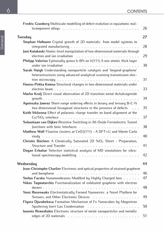
6 CONTENTS
Fredric Granberg Multiscale modelling of defect evolution in equiatomic mul-ticomponent alloys . . . . . . . . . . . . . . . . . . . . . . . . . . . . 26
Tuesday 27Stephan Hofmann Crystal growth of 2D materials: from model systems to
integrated manufacturing . . . . . . . . . . . . . . . . . . . . . . . . . 28Jani Kotakoski Atomic-level manipulation of two-dimensional materials through
electron and ion irradiation . . . . . . . . . . . . . . . . . . . . . . . 29Philipp Valerius Epitaxially grown h-BN on Ir(111) A one atomic thick layer
under ion irradiation . . . . . . . . . . . . . . . . . . . . . . . . . . . 30Sarah Haigh Understanding nanoparticle catalysts and ’beyond-graphene’
heterostructures using advanced analytical scanning transmission elec-tron microscopy . . . . . . . . . . . . . . . . . . . . . . . . . . . . . . 31
Hannu-Pekka Komsa Structural changes in two-dimensional materials underelectron beam . . . . . . . . . . . . . . . . . . . . . . . . . . . . . . . 33
Marko Kralj Direct visual observation of 2D transition metal dichalcogenidegrowth . . . . . . . . . . . . . . . . . . . . . . . . . . . . . . . . . . . 34
Agnieszka Jamroz Short-range ordering effects in binary and ternary B-C-Ntwo-dimensional hexagonal structures in the presence of defects . . . 35
Keith Mckenna Effect of polaronic charge transfer on band alignment at theCu/TiO2 interface . . . . . . . . . . . . . . . . . . . . . . . . . . . . . 37
Sebastiaan van Dijken Resistive Switching in All-Oxide Ferroelectric TunnelJunctions with Ionic Interfaces . . . . . . . . . . . . . . . . . . . . . . 38
Matthew Wolf Fluorine clusters at CeO2(111) - A DFT+U and Monte Carlostudy . . . . . . . . . . . . . . . . . . . . . . . . . . . . . . . . . . . 40
Christin Büchner A Chemically Saturated 2D SiO2 Sheet - Preparation,Structure and Transfer . . . . . . . . . . . . . . . . . . . . . . . . . . 41
Dogan Erbahar Selective statistical analysis of MD simulations for vibra-tional spectroscopy modelling . . . . . . . . . . . . . . . . . . . . . . 42
Wednesday 44Jean-Christophe Charlier Electronic and optical properties of strained graphene
and borophene . . . . . . . . . . . . . . . . . . . . . . . . . . . . . . 46Stefan Facsko Nanomembranes Modified by Highly Charged Ions . . . . . . 47Nikos Tagmatarchis Functionalization of exfoliated graphene with electron
donors . . . . . . . . . . . . . . . . . . . . . . . . . . . . . . . . . . . 48Yossi Rosenwaks Electrostatically Formed Nanowires: a Novel Platform for
Sensors, and Other Electronic Devices . . . . . . . . . . . . . . . . . 49Flyura Djurabekova Formation Mechanism of Fe Nanocubes by Magnetron
Sputtering Inert Gas Condensation . . . . . . . . . . . . . . . . . . . 50Ioannis Remediakis Electronic structure of metal nanoparticles and metallic
edges of 2D materials . . . . . . . . . . . . . . . . . . . . . . . . . . 51
Ge
ne
ral
CONTENTS 7
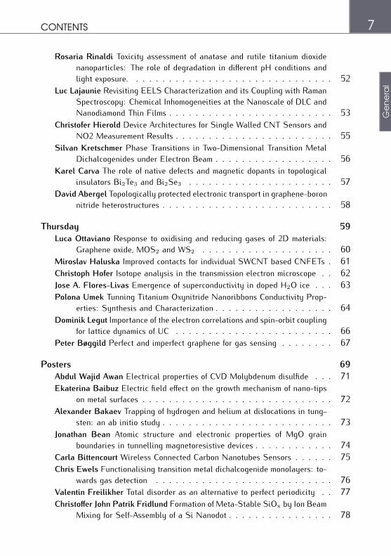
Rosaria Rinaldi Toxicity assessment of anatase and rutile titanium dioxidenanoparticles: The role of degradation in different pH conditions andlight exposure. . . . . . . . . . . . . . . . . . . . . . . . . . . . . . . 52
Luc Lajaunie Revisiting EELS Characterization and its Coupling with RamanSpectroscopy: Chemical Inhomogeneities at the Nanoscale of DLC andNanodiamond Thin Films . . . . . . . . . . . . . . . . . . . . . . . . . 53
Christofer Hierold Device Architectures for Single Walled CNT Sensors andNO2 Measurement Results . . . . . . . . . . . . . . . . . . . . . . . . 55
Silvan Kretschmer Phase Transitions in Two-Dimensional Transition MetalDichalcogenides under Electron Beam . . . . . . . . . . . . . . . . . . 56
Karel Carva The role of native defects and magnetic dopants in topologicalinsulators Bi2Te3 and Bi2Se3 . . . . . . . . . . . . . . . . . . . . . . 57
David Abergel Topologically protected electronic transport in graphene-boronnitride heterostructures . . . . . . . . . . . . . . . . . . . . . . . . . . 58
Thursday 59Luca Ottaviano Response to oxidising and reducing gases of 2D materials:
Graphene oxide, MOS2 and WS2 . . . . . . . . . . . . . . . . . . . . 60Miroslav Haluska Improved contacts for individual SWCNT based CNFETs . 61Christoph Hofer Isotope analysis in the transmission electron microscope . . 62Jose A. Flores-Livas Emergence of superconductivity in doped H2O ice . . . 63Polona Umek Tunning Titanium Oxynitride Nanoribbons Conductivity Prop-
erties: Synthesis and Characterization . . . . . . . . . . . . . . . . . . 64Dominik Legut Importance of the electron correlations and spin-orbit coupling
for lattice dynamics of UC . . . . . . . . . . . . . . . . . . . . . . . . 66Peter Bøggild Perfect and imperfect graphene for gas sensing . . . . . . . . 67
Posters 69Abdul Wajid Awan Electrical properties of CVD Molybdenum disulfide . . . 71Ekaterina Baibuz Electric field effect on the growth mechanism of nano-tips
on metal surfaces . . . . . . . . . . . . . . . . . . . . . . . . . . . . . 72Alexander Bakaev Trapping of hydrogen and helium at dislocations in tung-
sten: an ab initio study . . . . . . . . . . . . . . . . . . . . . . . . . . 73Jonathan Bean Atomic structure and electronic properties of MgO grain
boundaries in tunnelling magnetoresistive devices . . . . . . . . . . . . 74Carla Bittencourt Wireless Connected Carbon Nanotubes Sensors . . . . . . 75Chris Ewels Functionalising transition metal dichalcogenide monolayers: to-
wards gas detection . . . . . . . . . . . . . . . . . . . . . . . . . . . 76Valentin Freilikher Total disorder as an alternative to perfect periodicity . . 77Christoffer John Patrik Fridlund Formation of Meta-Stable SiOx by Ion Beam
Mixing for Self-Assembly of a Si Nanodot . . . . . . . . . . . . . . . . 78
Ge
ne
ral

8 CONTENTS
Seyed Arsalan Hashemi Petrudi Phonon in single-layer transition metaltrichalcogenides . . . . . . . . . . . . . . . . . . . . . . . . . . . . . . 79
Eero Holmstrom Adsorption of H2O onto SrTiO3 from DFT, hybrid-functionalDFT, and MP2 . . . . . . . . . . . . . . . . . . . . . . . . . . . . . . 80
Anne Holtsch Analysis of local variations of the electronic properties of mono-and bilayer graphene/HOPG . . . . . . . . . . . . . . . . . . . . . . . 81
Anne Holtsch Analysis of Atomic Moiré patterns on Graphene/Rh(111) . . . 82Stefan Hummel Mechanical and Electrical Study of 2D materials by novel
Dual-Probe Atomic force- /Scanning tunneling microscope . . . . . . . 83Sampo Inkinen In-situ TEM Observation of Oxygen Vacancy Driven Struc-
tural and Resistive Phase Transitions in La2/3Sr1/3MnO3 . . . . . . . 84Federico Iori Engineering SrTiO3/LaAlO3 heterostructures thickness: an ab
initio study . . . . . . . . . . . . . . . . . . . . . . . . . . . . . . . . 85Marc Jäger Describing MoS2 Nanoclusters with Classical Potentials . . . . 86Elvar Örn Jónsson Self-interaction corrected energy functionals and Pipek-
Mezey orbital localization . . . . . . . . . . . . . . . . . . . . . . . . 87Shawulienu Kezilebieke Local Electronic Structure of a Magnetic Dimer
Impurity in a Superconductor . . . . . . . . . . . . . . . . . . . . . . . 89Byung-Hyun Kim Multiscale modelling of CeO2 nano-interfaces . . . . . . . 90Franciszek Krok Formation of hexagonal gold nanostructures during self-
assembling on Ge(001) surface . . . . . . . . . . . . . . . . . . . . . . 91Artem Kuklin Theoretical Prediction of One-Atom-Thick Hexagonal CrN:
Electronic Structure and Magnetic Properties . . . . . . . . . . . . . 92Andreas Kyritsakis A general computational method for electron emission
and thermal effects in field emitting nanotips . . . . . . . . . . . . . . 94Eduard Llobet MHDA-Functionalized carbon nanotubes for detecting non-
aromatic VOCs and warfare agents . . . . . . . . . . . . . . . . . . . 95Alvaro Lopez Cazalilla Nanoripples production on a-Si surfaces under Ar
irradiation . . . . . . . . . . . . . . . . . . . . . . . . . . . . . . . . . 96Ursula Ludacka Straining free-standing 2D materials in a TEM . . . . . . . 97Ales Mrzel Molybdenum carbide and superconducting nitride nanowires:
facile synthesis, transport measurements and their use as transparentelectrodes . . . . . . . . . . . . . . . . . . . . . . . . . . . . . . . . . 98
Kimmo Mustonen Buckyball Sandwiches . . . . . . . . . . . . . . . . . . . 99Alexei Nazarov Study of carbon nanostructures generated by gamma irradi-
ation of graphene flakes on nickel . . . . . . . . . . . . . . . . . . . . 100Mildred Quintana Graphene processing towards applications . . . . . . . . 102Isaac Tamblyn First principles training sets and atomistic potentials for
boron-nitride nanostructures . . . . . . . . . . . . . . . . . . . . . . . 103Dmitry Terentyev Carbon-vacancy complexes controlling nano-scale irradia-
tion damage in iron and steels . . . . . . . . . . . . . . . . . . . . . . 104Camilla Tossi Conversion of light for the production of fuels using cell factories105
Ge
ne
ral

CONTENTS 9
Henrique Vazquez Muinos Creating nanoporous graphene with swift heavyions . . . . . . . . . . . . . . . . . . . . . . . . . . . . . . . . . . . . 106
David Visontai Controlling Josephson current with topological states in bi-layer graphene . . . . . . . . . . . . . . . . . . . . . . . . . . . . . . 107
Lide Yao In-Situ Transmission Electron Microscopy of Functional Materials . 108Junle Zhao Multi-step growth and emission mechanism in matrix assembly
cluster source . . . . . . . . . . . . . . . . . . . . . . . . . . . . . . . 109Shengqiang Zhou Colossal Enhancement in Magnetic Moment of Ferrimag-
netic NiCo2O4 via Strain-Doping . . . . . . . . . . . . . . . . . . . . 110
Participants 111
Index 113
Ge
ne
ral

10 CONTENTS
Ge
ne
ral

Oral presentations 11
Monday 13.02.20178:40 - 8:45 Intro8:45 - 9:00 Capan
Information on NATO SPS programmechair: Hoffmann
9:00 - 9:40 SwagerChemical Sensors for Explosives and CW Detection
9:40 - 10:20 LiljerothAtomically precise graphene nanoribbons through on-surface synthesis
10:20 - 10:40 BloodDesign and Implementation of the Chemical Warfare Agent Force Field
10:40 - 11:20 Coffee
chair: Hierold11:20 - 12:00 Jelinek
Exploring structural and electronic properties of helical molecules on surfaces.12:00 - 12:20 Biel
SPM fingerprints and electronic properties of point-like and extended defects in single-layer MoS2
12:20 - 12:40 Rio1D and 2D networks of cyclo-paraphenylenes (CPPs) using covalent and self-assemblyprocess by DFT
12:40 - 13:00 DebliquyFormaldehyde detection for indoor air quality
13:00 - 16:40 Lunch16:40 - 17:00 Coffee
chair: McKenna17:00 - 17:40 Kawai
On-surface chemical reaction and its product studied by high-resolution atomic forcemicroscopy
17:40 - 18:00 GulansPhotoabsorption of adsorbed azobenzene monolayers: impact of graphene substrate
18:00 - 18:20 SchulzElemental contrast in noncontact atomic force microscopy on a boron-nitride monolayer
18:20 - 18:40 JónssonSemi-infinite solid approach to calculations of surface properties
18:40 - 19:00 GranbergMultiscale modelling of defect evolution in equiatomic multicomponent alloys

12 Oral presentations
Mo
nd
ay

Oral presentations 13
Chemical Sensors for Explosives and CW Detection
T. M. Swager11Massachusetts Institute of Technology
This lecture will detail the creation of ultrasensitive sensors based on elec-tronically active conjugated polymers (CPs) and carbon nanotubes (CNTs). Acentral concept that a single nano- or molecular-wire spanning between twoelectrodes would create an exceptional sensor if binding of a molecule of inter-est to it would block all electronic transport. The use of molecular electroniccircuits to give signal gain is not limited to electrical transport and CP-basedfluorescent sensors can provide ultratrace detection of chemical vapors via am-plification resulting from exciton migration. Nanowire networks of CNTs providefor a practical approximation to the single nanowire scheme and selectivity isgenerated by covalent and/or non-covalent binding selectors/receptors to thecarbon nanotubes. Sensors for a variety of materials and cross-reactive sensorarrays will be described. Polar hydrogen bonding groups provide selectivityfor nitro-groups and methods for responding to electrophilic chemical weaponswill also be detailed.
[1] Yang, J.-S.; Swager, T. M. Porous Shape Persistent Fluorescent Polymer Films: An Approachto TNT Sensory Materials J. Am. Chem. Soc. 1998, 120, 5321-5322.
[2] Schnorr, J. M.; van der Zwaag, D.; Walish, J. J.; Weizmann, Y.; Swager, T. M. Sensory Arrays ofCovalently Functionalized Single-Walled Carbon Nanotubes for Explosive Detection Adv.Funct. Mater. 2013, 23, 5285-5291.
[3] Wang, F.; Gu, H.; Swager, T. M. Carbon Nanotube/Polythiophene Chemiresistive Sensors forChemical Warfare Agents J. Am. Chem. Soc. 2008, 130, 5392-5393.
[4] Weis, J. G.; Swager, T. M. Thiophene-fused Tropones as Chemical Warfare Agent-ResponsiveBuilding Blocks ACS Macro Lett., 2015, 4, 138-142.
[5] Belger, C.; Weis, J. G.; Ahmed, E.; Swager, T. M. Colorimetric Stimuli-Responsive HydrogelPolymers for the Detection of Nerve Agents Macromolecules 2015, 48, 7990-7994.
[6] Ishihara, S.; Azzarelli, J. M.; Swager T. M. Ultratrace Detection of Toxic Chemicals: TriggeredDisassembly of Supramolecular Nanotube Wrappers J. Am. Chem. Soc. 2016, 138, 8221-8227.
[7] Zhu, R.; Azzarelli, J. M.; Swager, T. M. Wireless Hazard Badges for Nerve Agent SimulantsAngew. Chem. Int. Ed. 2016, 55, 9662-9666.
Mo
nd
ay

14 Oral presentations
Atomically precise graphene nanoribbons through on-surfacesynthesis
P. Liljeroth1
1Department of Applied Physics, Aalto University School of Science, PO Box 15100, 00076Aalto, Finland
Graphene nanoribbons (GNRs) are a new class of materials that have promisingapplications in next-generation nanoelectronic, photonic and spintronic devices.GNRs have been predicted to show interesting electronic properties that dependstrongly on their width and edge structure. However, the required precisioncannot be achieved by top-down approaches, including e-beam lithographyon a sheet of graphene or unzipping carbon nanotubes. Recently, bottom-upsynthesis using molecular precursors has been shown to provide precise controlover the width and edge geometry of GNRs [1]. By changing the monomerdesign, fabrication of a wide range of different GNRs can be achieved withengineered chemical and electronic properties.
In the typical picture of the on-surface synthesis, the substrate does not playa big role in the chemical reaction. Using low-temperature scanning tunnelingmicroscopy (STM) and atomic force microscopy (AFM), I will show that thesubstrate is not always an innocent bystander in these reactions. On Au(111)surface, the prototypical precursor dibromo-bianthryl (DBBA) polymerizes viaan Ullmann route to form straight GNRs with armchair edges. However, onCu(111), the DBBA precursor forms chiral (3,1)GNRs. In contrast, dibromo-perylene (DBP) precursors do form armchair GNRs via Ullmann coupling, inclose analogy to recent results on Au(111). The reaction intermediates highlightthe role of the precursor shape, molecule-molecule interactions and substratereactivity as decisive factors in determining the reaction pathway [2]. Our find-ings help to realize new routes for previously unattainable covalently bondednanostructures.
The armchair GNRs can be divided into three families based on their widthN: GNRs with N=3m or N=3m+1, where m is an integer, are semiconduct-ing. On the other hand, GNRs with a width of N=3m+2 are predicted to benearly metallic with a very small bandgap. We have synthesized N=5 armchairGNRs and studied their electronic properties in detail using low-temperaturescanning probe techniques [3]. Scanning tunneling spectroscopy demonstratesthat N=5 ribbons show nearly metallic behavior with much smaller bandgapthan the wider N=7 GNRs belonging to the N=3m+1 family. These nar-row armchair GNRs with a small bandgap would form ideal molecular wiresto be used as interconnects in molecular scale circuitry. In addition mono-component GNRs, we have realized metal-semiconductor heterostructures by
Mo
nd
ay

Oral presentations 15
joining armchair GNRs belonging to the metallic (5-atom wide) and semicon-ducting (7-atom wide) families through on-surface synthesis. These structuresconstitute the first steps towards enco ding more functionality into a singleGNR for electronic applications.
[1] L. Talirz, P. Ruffieux, R. Fasel, Adv. Mater. 28, 6222 (2016).[2] F. Schulz et al., submitted (2016).[3] A. Kimouche et al., Nat. Commun. 6, 10177 (2015).
Mo
nd
ay

16 Oral presentations
Design and Implementation of the Chemical Warfare AgentForce Field
J. W. Blood1 K. E. Jelfs1 J. Jones21Department of Chemistry, Imperial College London, South Kensington Campus, London, SW72AZ
2 DSTL, Porton Down, Salisbury, SP4 0JQ
In recent months there have been continuing reports of chemical warfare agents(CWAs) being used in conflict situations in Syria.[1] How these chemicals reactwith the body is well understood, however it is less clear how they interactwith porous materials they can encounter in the field, such as sand, brick, soil,etc. Molecular simulations are an ideal way to investigate these highly toxicchemicals at an atomistic level. To this end we present the Chemical WarfareAgent Force Field (CWAFF), which has been parameterised to describe thenerve agents GB, VX, and VM, as well as the vesicant HD.
CWAFF has been used to model agent behaviour in a variety of substrateschosen to mimic chemical functionalities of materials with which the agentscould come into contact. In order to obtain a more comprehensive understandingof the sorption and diffusion of CWAs, both organic and inorganic host materialswere chosen, with a variety of chemical moieties and pore sizes. CWAFF hasbeen implemented with DL_POLY[2] for molecular dynamics simulations andRASPA[3] for Grand Canonical Monte Carlo simulations.
[1] Associated Press, The Guardian https://www.theguardian.com/world/2016/aug/25/assad-regime-isis-chemical-attacks-syria-un-investigators(2016).
[2] I. T. Todorov, W. Smith, K. Trachenko, M. T. Dove, M. R. S. Pinches, D. Tildesley, W. Smith, D.Rapaport, M. E. Tuckerman, B. J. Berne, G. J. Martyna, G. J. Martyna, M. E. Tuckerman, J. T.Douglas, M. L. Klein, H. C. Andersen, U. Essmann, L. Perera, M. L. Berkowtz, T. Darden, H.Lee, L. G. Pedersen, D. E. Shaw, X. L. Cao, Z. Y. Mo, I. T. Todorov, W. Smith, W. Smith, W.Smith, T. R. Forester, M. D. Segall, P. J. D. Lindan, M. J. Probert, C. J. Pickard, P. J. Hasnip, S.J. Clark, M. C. Payne1, J. P. Ryckaert, G. Ciccotti, H. J. C. Berendsen, W. C. Swope, H. C.Andersen, P. H. Berens, K. R. Wilson, J. Tersoff, P. J. D. Lindan, M. J. Gillan, S. A. Adelman, J.Doll, J. A. Izaguirre, K. Trachenko, M. T. Dove, T. G. W. Geisler, I. T. Todorov, W. Smith, K.Trachenko, M. T. Dove, E. K. H. Salje, I. T. Todorov, W. Smith, M. Pruneda, E. Artacho, K.Trachenko, I. T. Todorov, M. T. Dove, W. Smith, I. T. Todorov, J. A. Purton, N. L. Allan, M. T.Dove, M. Berkowitz, J. , J. Mater. Chem. 16, 1911 (2006).
[3] D. Dubbeldam, S. Calero, D. E. Ellis and R. Q. Snurr, Mol. Simul. 7022, 1-21 (2015).
Mo
nd
ay

Oral presentations 17
Exploring structural and electronic properties of helicalmolecules on surfaces.
P. Jelinek11Institute of Physics of the CAS, Prague, Czech republic
Molecules with helical structure fascinate chemists for many years due to theirnonplanar structure, which introduces inherently chirality and it exhibits inter-esting optical and electronic properties. We will present two different studiesof helicene molecules on metal surfaces to explore: i) chirality transfer drivenby on-surface reaction and ii) their mechanical response to an external field. Inthe first case, we will demonstrate that transfer chirality from a homochiral heli-cal precursor to enantiofacially adsorbed prochiral products through a cascadeof stereoconservative on-surface reactions is possible [1]. Detailed molecularstructure of intermediates and final products of the chemical reactions, includ-ing their chirality, are identified by means of high-resolution SPM imagessupported by extensive theoretical DFT-based analysis. In the second case, wewill report simultaneous tunneling current and force through helicene moleculesdeposited on Ag(111) surface. We will show that simultaneous AFM/STM mea-surements together with DFT calculations reveals strong piezoelectric effectdetected on a single molecule on metal surface.
[1] O. Stetsovych et al, , Nature Chemistry 10.1038/nchem.2662 (2016).
Mo
nd
ay
18 Oral presentations
SPM fingerprints and electronic properties of point-like andextended defects in single-layer MoS2
C. Gonzalez1,2,3 E. R. Ortiz1 Y. Dappe2 B. Biel1,31Departamento de Electronica y Tecnologia de Computadores, Universidad de Granada, Campusde Fuente Nueva, 18071 Granada, Spain
2SPEC, CEA, CNRS, Universite Paris-Saclay, CEA Saclay 91191 Gif-sur-Yvette Cedex, France3CITIC, Campus de Aynadamar, 18071 Granada, Spain
Defects, commonly created during the growth process in two-dimensional (2D)materials, can dramatically modify the performance of 2D-based devices. In thecase of MoS2, a transition metal dichalcogenide (TMD) semiconductor with adirect gap of 1.8 eV [1] with promising applications in nanoelectronics, manyof these defects have already been observed, of both the point-like [2] andextended kinds [3]. However, with the exception of the S monovacancy, a de-tailed characterization of their electronic, magnetic and transport features isstill lacking.
A valuable tool for identifying the properties of such defects is ScanningProbe Microscopy (SPM). However, the interpretation of the images producedvia this technique is not always straightforward and often requires the helpof atomic-scale simulations to provide a correct understanding of the sampleunder study.
In this work, we present an ab initio study of the most common point-likedefects observed in monolayer MoS2. The investigation of several types of grainboundaries that may appear in polycrystalline MoS2 has been addressed aswell. We analyze the electronic and transport features of the selected defects[4,5] and supply their simulated images for both the Scanning Tunneling (ST)[6] and Atomic Force (AF) [7] Microscopy techniques.
We expect our work to provide a valuable tool for experimentalists and tohelp improve the understanding of the electronic and transport properties ofdefected MoS2 monolayers.
[1] K.F. Mak et al., Physical Review Letters 105, 136805 (2010).[2] J. Hong et al., Nature Communications 6, 6293 (2015).[3] Y.L. Huang et al., Nature Communications 6, 6298 (2015).[4] E.R. Ortiz and B. Biel, (in preparation).[5] C. Gonzalez, Y. Dappe and B. Biel, (in preparation).[6] C. Gonzalez, B. Biel and Y. Dappe, Nanotechnology 27, 105702 (2016).[7] C. Gonzalez, Y. Dappe and B. Biel, The Journal of Physical Chemistry C 120, 17115 (2016).
Mo
nd
ay
Oral presentations 19
1D and 2D networks of cyclo-paraphenylenes (CPPs) usingcovalent and self-assembly process by DFT
J. Rio1 D. Erbahar2 P. Briddon3 N. Tagmatarchis4 H. A. Wegner5 C. Ewels11Institut des Matériaux Jean Rouxel (IMN), Université de Nantes, CNRS UMR 6502, F-44322Nantes, France
2Physics Department, Gebze Technical University, Gebze, Turkey3School of Electrical and Electronic Engineering, University of Newcastle, Newcastle upon Tyne,NE 1 7RU, UK
4Theoretical and Physical Chemistry Institute, National Hellenic Research Foundation, Athens,Greece
5Institute of Organic Chemistry, Justus Liebig University, Heinrich-Buff-Ring 17, 35392 Giessen,Germany
Cycloparaphenylenes (CPPs) represent the shortest possible segment of (n,n)armchair carbon nanotubes (CNTs), and as such may represent a new route toproducing chirally selected carbon nanotubes [1] [2]. Current approaches forthis envisage controlling synthesis of uniform-diameter single chirality CNTsusing CPPs as templates, which has met with limited success [3]. At the sametime complexes of fullerenes with CPPs have been reported, highlighting a highsize selectivity of the CPPs to the specific fullerene.
In the current study we explore a new approach, namely using covalent- andnon-covalent self-assembly of either functionalized CPPs, or CPP-C60 hybridsystems, to create new types of poly-CPP-nanotubes. These new materials,while also adopting a controlled chirality tubular morphology, show distinctlydifferent chemical, mechanical, electronic and optical behavior to conventionalcarbon nanotubes.
The first of these families involves chemical cross-linking between neigh-bouring CPPs using fullerenes as alignment templates. The resultant poly-CPP-nanotubes share some properties with conjugated polymers, notably theability to add functionality and control electronic properties through function-alisation control. The second family using self-assembly stacking between C60
and different sizes of [6]-, [8]-, [10]-CPPs to form 1D and 2D networks. While thestudy is driven by our theoretical modelling, we successfully demonstrate viaa joint experimental-theoretical study the first steps towards their production,namely trapping of 2CPP rings around a fullerene dimer (C59N)2 [4].[1] A.-F. Tran-Van, E. Huxol, J. M. Basler, M. Neuburger, J.-J. Adjizian, C. P. Ewels and H. A.
Wegner, Org. Lett. 16, 1594-1597 (2014).[2] J. Rio, D. Erbahar, M. Rayson, P. Briddon and C. P. Ewels, Phys. Chem. Chem. Phys. 18,
23257-23263 (2016).[3] H. Omachi, T. Nakayama, E. Takahashi, Y. Segawa and K. Itami, Nat. Chem. 5, 572-576
(2013).[4] J. Rio, S. Ahles, C. Ewels, D. Jacquemin, N. Tagmatarchis, H. A. Wegner, in preparation .
(2017).
Mo
nd
ay

20 Oral presentations
Formaldehyde detection for indoor air quality
M. Debliquy1 D. Lahem2 X. Tang3 L. Bilteryst4 J. Raskin3
1Materials Science Department, University of Mons2Materia Nova3ICTEAM University of Louvain-La-Neuve4CERTECH
Volatile Organic Compounds in indoor air have become these last years the sub-ject of a big concern. The main emission sources are: furniture, paintings, var-nishes, wood protection, construction materials, etc. In particular, formaldehydeis now considered by the authorities as one of the priority pollutants because ofits carcinogenic [1] character and because of the multiplication of sources in ourclose environment. The World Health Organization (WHO) guideline for indoorair formaldehyde concentration is 80 ppb (0.1 mg/m3) [2]. Methods based on airsample collection and lab measurements are available and are the most usedmethods [3]. They are accurate and reliable but these methods are expensive,are not real time and some statistics issues are raised because of that. That iswhy, it is important to detect and measure formaldehyde in real time, in situand with a low cost equipment. Devices based on chemical sensors are a goodsolution as these systems can be ve ry sensitive, low cost and easily integratedin common electronics to build portable systems [4]. Different sensing tech-nologies exist and we will focus on electrochemical systems exploiting organicor inorganic semiconductor materials. These sensors are based on the mon-itoring of the conductivity changes of a semiconducting sensitive coating dueto a reversible doping by the adsorbed gases. This paper will shortly presenta overview of the existing sensors for formaldehyde detection and new sensorsbased on metal oxides and on the use of molecularly imprinted polymers. Metaloxide gas sensors are well known for their high sensitivity allowing detectionin the ppb concentration range and their stability. The main drawback is thatthey generally need to be heated to temperatures in the range 150-350C. Inorder to reduce the power consumption, the area of the sensitive layer is minia-turized using MEMS technology. Our sensor with an area of 200x200 µm2consumes a power of 15mW when it operates continuously. The concentrationrange for formaldehyde is 10-2000 ppb. Molecularly imprinted polymers (MIP)are polymers that are synthesized incorporating the target molecule we want todetect as a template. Functional monomers form a complex around the templateand are linked afterwards to form a polymer constituted of a series of ”cages”trapping the template. Once the synthesis is complete, the template moleculeis extracted, leaving a molecular cavity imprinted in the polymer matrix thatallows the polymer to selectively recognize the target molecule [5]. These ele-ments are cheap, easy to synthesize and can be adapted to any kind of surface.
Mo
nd
ay

Oral presentations 21
Using conducting polymers for building MIPs allows to get semiconductor gassensors working at room temperature with a good selectivity. We succeededin preparing sensors based on polypyrrole deposited by electropolymerizationdetecting formaldehyde in the range [100 ppb-20 ppm].
[1] IARC Working Group, IARC monographs on the evaluation of carcinogenic risks to humans,World Health Organization 88, 39-325 (2006).
[2] World Health Organization, Regional Office for Europe, Selected pollutants: WHO guidelinefor indoor air quality ISBN: 9789289002134, 142 (2010).
[3] A. Vairavamurthy, J.M. Roberts, L. Newman, Atmos. Environ 26A, 1965-1993 (1992).[4] P.-R. Chung, C.-T. Tzeng, M.-T. Ke and C.-Y. Lee, Sensors 13, 4468-4484 (2013).[5] K. Haupt, A. V. Linares, M. Bompart, B. T. S. Bui, Molecularly Imprinted Polymers„ Ed.,
Springer Berlin Heidelberg 1-28 (2011).
Mo
nd
ay

22 Oral presentations
On-surface chemical reaction and its product studied byhigh-resolution atomic force microscopy
S. Kawai11International Center for Materials Nanoarchitectonics, National Institute for Materials Science2Department of Physics, University of Basel3PRESTO, Japan Science and Technology Agency
Since the first direct observation of the chemical structure of pentacene, atomicforce microscopy (AFM) became a powerful tool for surface chemistry [1]. Suchhigh-resolution imaging technique is quite beneficial to identify structures ofmolecules condensed by the C-H· · ·F hydrogen bonding [2], halogen bonding[3], and two-dimensional metal organic framework [4] and of the doped graphenenanoribbons [5] and novel aromatic compounds [6] synthesized by on-surfacechemical reaction. Furthermore, the synthesized products as polyfluorene [7]and graphene nanoribbon [8] can be used for measurement of the mechanicalproperties, in which the effect of the commensurability and incommensurabilityplays a role in friction during lifting and sliding the objects.
[1] L. Gross et al., Science 325, 1110 (2009).[2] S. Kawai et al., ACS Nano 7, 9098 (2013).[3] S. Kawai et al., ACS Nano 9, 2574 (2015).[4] S. Kawai et al., Nat. Commun. 7, 11559 (2016).[5] S. Kawai et al., Nat. Commun. 6, 8098 (2015).[6] S. Kawai et al., Nat. Commun. 7, 12711 (2016).[7] S. Kawai et al., Proc. Natl. Acad. Sci. USA 111, 3968 (2014).[8] S. Kawai et al., Science 351, 957 (2016).
Mo
nd
ay

Oral presentations 23
Photoabsorption of adsorbed azobenzene monolayers: impactof graphene substrate
Q. Fu1 C. Cocchi1 D. Nabok1 A. Gulans1 C. Draxl11Institut für Physik and IRIS Adlershof, Humboldt-Universität zu Berlin
We use density-functional theory and many-body perturbation theory to studythe impact of the graphene substrate on the photo-absorption properties oftrans- and cis-azobenzene monolayers. The molecules are weakly bound tographene, and their orbitals are essentially not hybridized with bands of thesubstrate. Yet graphene remarkably modulates the absorption spectra of the ad-sorbates. Firstly, it influences excitation energies via (i) substrate polarizationreducing the band-gap of azobenzene and (ii) enhanced dielectric screening,which weakens the attractive interaction between electrons and holes. Sec-ondly, graphene activates intermolecular excitations, which are dark in the iso-lated monolayers. Our results demonstrate that the photoisomerization processof weakly adsorbed azobenzene undergoes notable changes on the carbon-based substrate compared to the isolated monolayers.
Mo
nd
ay

24 Oral presentations
Elemental contrast in noncontact atomic force microscopy on aboron-nitride monolayer
F. Schulz1,2 J. Ritala2 A. P. Seitsonen3 A. S. Foster2 P. Liljeroth2
1IBM Research, Zurich Research Laboratory, 8803 Rüschlikon, Switzerland2Department of Applied Physics, Aalto University School of Science, 00076 Aalto, Finland3Départment de Chimie, École Normale Supérieure, 75005 Paris, France
Elemental contrast with atomic resolution is a key aspect of cutting-edge mi-croscopy, enabling materials research at the nanoscale. Transmission elec-tron microscopy (TEM) offers chemical sensitivity through different modes, moststrikingly as Z-contrast and via atomically resolved electron energy loss spec-troscopy (EELS) in scanning TEM [1]. However, due to the high-energy electronbeam, TEM is not suitable for more sensitive structures such as small organicmolecules. A less destructive alternative might be noncontact atomic force mi-croscopy (nc-AFM). Though not yet capable of chemical fingerprinting as pow-erful as EELS, elemental contrast is one of the most-studied topics in nc-AFM.In a seminal contribution, Sugimoto et al. identified different atomic species ina surface alloy by comparing the maximum attractive forces on different latticesites in ∆f(z) spectroscopy [2]. Measurements of the local contact potentialdifference (LCPD) in Kelvin probe force microscopy, either via an AC modulationof the tip-sample voltage or through ∆f(V ) spectroscopy, is another avenuethat achieved chemical resolution, in particular on ionic systems [3-5]. Here, weemploy nc-AFM with CO-functionalized tips [6] to investigate the atomic-scalecontrast on a monolayer of hexagonal boron nitride (hBN) on Ir(111) [7]. hBNconstitutes an interesting model system, as it is a mostly covalently bondedinsulator with a nearest-neighbour distance of only ∼ 145 pm. Yet constant-height maps of both frequency shift and local contact potential difference revealstrong contrast between the boron and nitrogen sub-lattices. nc-AFM simula-tions based on the density functional theory-optimized hBN/Ir(111) geometryallow us to match the two distinct atomic sites with the different elementsand shine light on the origin of the atomic-scale contrast. Our combinationof constant-height images and atomically resolved LCPD maps offers a robustmethod to identify different chemical species in nc-AFM.
[1] K. W. Urban, Science 321, 506 (2008).[2] Y. Sugimoto et al., Nature 446, 64 (2007).[3] F. Bocquet et al., Phys. Rev. B 78, 035410 (2008).[4] G. H. Enevoldsen et al., Phys. Rev. Lett. 100, 236104 (2008).[5] L. Gross et al., Phys. Rev. B 90, 155455 (2014).[6] L. Gross et al., Science 325, 5944 (2009).[7] F. Schulz et al., Phys. Rev. B 89, 235429 (2014).
Mo
nd
ay

Oral presentations 25
Semi-infinite solid approach to calculations of surfaceproperties
S. Smidstrup1 T. K. Ghosh2 E. Jonsson2 K. Stokbro1 H. Jónsson2,3
1QuantumWise, Copenhagen, Denmark2Department of Applied Physics, Aalto University, Finland3Faculty of Physical Sciences, University of Iceland
A method for carrying out electronic density functional theory calculations ofsurface properties using a semi-infinite solid model and a fixed chemical po-tential of electrons is presented along with various applications to metal andsemiconductor surfaces. A Green function approach [1] is used to simulate asystem consisting of two regions: (A) the bulk solid represented by a mini-mal unit cell and subject to periodic boundary conditions in three dimensions,and (B) a surface region represented by a few atomic layers subject to peri-odic boundary conditions in two dimensions with a free surface on one sidebut matched to region (A) on the other side. Not only is this a more accuratedescription of a solid surface but the computational effort is also an order ofmagnitude smaller than with the commonly used slab model. The semi-infinitesolid approach has been implemented in the ATK software using atomic basissets. Results of calculations demonstrate fast and system atic convergence of,for example, work function and band gap with the number of layers in region(B), while results of slab calculations show erratic convergence or even lack ofconvergence with the number of layers in a slab. This new methodology opensup new possibilities for simulating the properties of thin films and nanostruc-tures on surfaces where the coupling to the substrate is properly taken intoaccount.
[1] M. Brandbyge, J-L. Mozos, P. Ordejon, J. Taylor, and K. Stokbro, Phys. Rev. B 65, 165401(2002).
Mo
nd
ay

26 Oral presentations
Multiscale modelling of defect evolution in equiatomicmulticomponent alloys
F. Granberg1 E. Levo1 F. Djurabekova1,2 K. Nordlund1
1Department of Physics, University of Helsinki2Helsinki Institute of Physics, University of Helsinki
High entropy alloys, and a sub category of them, equiatomic multicomponentalloys, have shown both good mechanical and corrosion resistant properties,desired in future nuclear power plant concepts. The alloys have good mechan-ical properties both at cryogenic temperatures as well as at high temperatures.But to use them in environments where radiation is present, it is crucial to knowtheir radiation response. In recent studies it have been found, both computa-tionally and experimentally, that they also show a reduction in accumulateddefects, compared to their elemental materials [1,3]. It was found that one keymechanisms of this reduction was the mobility of dislocations [1,2,3]. The resultsshow that the binary NiFe and the ternary NiCoCr and NiCoFe all show betterresponse to irradiation damage, compared to pure Ni and binary NiCo. Simu-lations of dislocation mobility show that the dislocations can easily move in Niand NiCo, whereas the other alloys show a lower mobility and a higher onsetstress. One of the key questions regarding especially nuclear power plants isthe long time evolution of the materials, when the expected lifetime of modernpower plant are over 50 years. To answer this question, we have started to usea multiscale approach to the problem, to assess the defect annealing and evolu-tion over longer timescales. The defect production is simulated with MolecularDynamics (MD), which can capture the picosecond primary damage production,and then use a Self Evolving Atomistic Kinetic Monte Carlo (SEAKMC) methodto assess the long time evolution. These two methods will be used consecu-tively after each other, first to produce the correct damage (with MD) and thenanneal it at timescales proportional to experimental ones (with SEAKMC).
[1] Granberg et. al, Physical Review Letters 116, 135504 (2016).[2] Granberg et al., Nuclear Instruments and Methods in Physics Research Section B , Accepted
for publication (2016).[3] Levo et al., In preparation , (2016).
Mo
nd
ay

Oral presentations 27
Tuesday 14.02.2017
chair: Liljeroth9:00 - 9:40 Hofmann
Crystal growth of 2D materials: from model systems to integrated manufacturing9:40 - 10:20 Kotakoski
Atomic-level manipulation of two-dimensional materials through electron and ion irra-diation
10:20 - 10:40 ValeriusEpitaxially grown h-BN on Ir(111) – A one atomic thick layer under ion irradiation
10:40 - 11:20 Coffee
chair: Charlier11:20 - 12:00 Haigh
Understanding nanoparticle catalysts and ’beyond-graphene’ heterostructures usingadvanced analytical scanning transmission electron microscopy
12:00 - 12:20 KomsaStructural changes in two-dimensional materials under electron beam
12:20 - 12:40 KraljDirect visual observation of 2D transition metal dichalcogenide growth
12:40 - 13:00 JamrozShort-range ordering effects in binary and ternary B-C-N two-dimensional hexagonalstructures in the presence of defects
13:00 - 16:40 Lunch16:40 - 17:00 Coffee
chair: Jonsson17:00 - 17:40 McKenna
Effect of polaronic charge transfer on band alignment at the Cu/TiO2 interface17:40 - 18:00 van Dijken
Resistive Switching in All-Oxide Ferroelectric Tunnel Junctions with Ionic Interfaces18:00 - 18:20 Wolf
Fluorine clusters at CeO2(111) - A DFT+U and Monte Carlo study18:20 - 18:40 Büchner
A Chemically Saturated 2D SiO2 Sheet - Preparation, Structure and Transfer18:40 - 19:00 Erbahar
Selective statistical analysis of MD simulations for vibrational spectroscopy modelling

28 Oral presentations
Crystal growth of 2D materials: from model systems tointegrated manufacturing
S. Hofmann1
1University of Cambridge
The commercial potential of 2D materials hinges on the development of growthand process techniques that are scalable and allow an adequate level of struc-tural control. Chemical vapor deposition (CVD) can uniquely serve the demandfor integrated manufacturing of electronic-grade large-area 2D material filmsas well as potentially allows the direct growth of vertical, stacked or uniquein-plane 2D heterostructures. Understanding the underlying crystal growthmechanisms is a current bottleneck and key future enabler. This talk will reviewour current understanding of graphene and h-BN CVD based on model catalystsystems, including results from a range of in-situ characterization methods suchas environmental scanning and transmission electron microscopy, high-pressureX-ray photoelectron spectroscopy, X-ray diffraction and scanning tunneling mi-croscopy [1-3]. We will outline the potential of direct CVD of various 2D het-erostructures as well as current challenges for integrated manufacturing andindustrial device integration of these 2D materials [4,5].
[1] Weatherup et al., Nano Lett 16, 6196 (2016).[2] Caneva et al., Nano Lett 16, 1250 (2016).[3] Weatherup et al., JACS 137, 13698 (2014).[4] Piquemal-Banci et al., Appl. Phys. Lett. 108, 102404 (2016).[5] Braeuninger et al., Chem. Mater. asap, asap (2016).
Tue
sda
y

Oral presentations 29
Atomic-level manipulation of two-dimensional materialsthrough electron and ion irradiation
J. Kotakoski11Faculty of Physic, University of Vienna, Austria
Despite the great promise of two-dimensional materials due to their excitingproperties, they are not always directly suitable for applications. One wayto tune the material properties is to manipulate the atomic structure usingparticle irradiation. However, as one might expect, this is challenging to do inthe case of extremely thin materials, where careful control over the irradiationenergy and solid understanding of the underlying atomic-scale phenomena arerequired.
Despite the challenges, electron and ion irradiation have recently evolvedinto powerful techniques to manipulation the atomic structure of two-dimensionalmaterials. At the same time, the recent advancements in aberration-correctedtransmission electron microscopy both provide means to directly image the ma-nipulated structures but also to fine tune them by inducing local structuralchanges and even to move defects and impurity atoms.
In this presentation, I will describe the advances in manipulating graphenewith electron irradiation (e.g., Ref. [1]) and overview our latest progress inusing ion irradiation at a large energy scale to implant foreign atoms intographene [2], moving impurity atoms and defects at will (e.g., Refs. [3,4]), creat-ing nanopores into graphene [5] and MoS2, patterning graphene with gratingsand two-dimensional amorphized areas [6,7] as well as other recent results.
If time allows, I will also describe our new experimental setup (to be finishedin 2017) combining low-energy ion irradiation line in the same vacuum as astate-of-the-art aberration-corrected scanning transmission electron miroscopefitted for in situ manipulation during imaging.
[1] Susi et al., Nat. Commun. 7, 13040 (2016).[2] Susi et al., ArXiv 1610.03419 (2016).[3] Kotakoski et al., Nat. Commun. 5, 4991 (2014).[4] Susi et al., Phys. Rev. Lett. 113, 115501 (2014).[5] Emmrich et al., Appl. Phys. Lett. 108, 163103 (2016).[6] Kotakoski et al., Nano Lett. 15, 5944 (2016).[7] Brand et al., Nat. Nanotech. 10, 845 (2015).
Tue
sda
y

30 Oral presentations
Epitaxially grown h-BN on Ir(111) A one atomic thick layerunder ion irradiation
P. Valerius1 C. Herbig1 M. Will1 M. A. Arman2 J. Knudsen2,3 V. Caciuc4N. Atodiresei4 S. Blügel4 T. Michely1
1II. Physikalisches Institut, Universität zu Köln, Zülpicher Str. 77, 50937 Köln, Germany2Division of Synchrotron Radiation Research, Lund University, Box 118, 22100 Lund, Sweden3MAX IV Laboratory, Lund University, Box 118, 22100 Lund, Sweden4Peter Grünberg Institut (PGI) and Institute for Advanced Simulation (IAS), ForschungszentrumJülich and JARA, 52425 Jülich, Germany
Chemical vapor deposition of B3N3H6 molecules on Ir(111) results in a wellaligned monolayer of hexagonal boron nitride (h-BN) which forms an incom-mensurate (11.7 x 11.7) moiré on (10.7 x 10.7) substrate unit cells. The centerof each unit cell provides a chemisorbed valley area, where h-BN is hybridizedwith the Ir substrate. Exposing such a monolayer of h-BN on Ir(111) at roomtemperature to low energy Xe+ irradiation causes amorphization of the 2Dlayer, as evidenced by low energy electron diffraction. The recovery processis followed up to 1550 K using scanning tunneling microscopy (STM), low en-ergy electron diffraction (LEED) and X-ray photoelectron spectroscopy (XPS).Surprisingly, upon annealing the h-BN layer and the moiré recover to goodperfection, except of blisters formed due to aggregation of implanted noble gasspecies, as well as vacancy clusters and larger vacancy islands resulting fromsputtering. With STM we image through the h-BN blister lid and find a super-structure corresponding in lattice parameter to what we expect for a crystalline,pressurized Xe. The blisters survive annealing to 1550 K, a temperature wherepristine h-BN on Ir(111) is already decomposed. They transform to a triangularshape, driven by the energetic preference of boron terminated edges. The ex-traordinary stability of Xe-filled triangular, boron-terminated h-BN blisters isconfirmed by dedicated DFT calculations. The vacancy clusters form an orderedarray of holes in the h-BN layer (a nanomesh), precisely at the locations of thevalleys, as there h-BN edges bind strongest to the substrate. Such a nanomeshmembrane could be well suited for water purification applications. Finally, wereport on experiments investigating the chemical reactivity of the valley regionby deposition of metallic and non-metallic elemental species, in order to deter-mine the suitability of the h-BN layer on Ir(111) as a template for aggregationof clusters, providing opportunities for nano-catalysis or nano-magnetism.
Tue
sda
y

Oral presentations 31
Understanding nanoparticle catalysts and ’beyond-graphene’heterostructures using advanced analytical scanningtransmission electron microscopy
S. J. Haigh1
1University of Manchester, School of Materials
The current generation of aberration corrected scanning transmission electronmicroscope (STEM) instruments optimized for high spatial resolution energydispersive x-ray (EDX) spectroscopy provide exciting opportunities for struc-tural and elemental analysis of nanoscale objects. Here I will discuss recentexample applications from our studies of nanoparticle catalysts and 2D deviceheterostructures where these analytical capabilities have provided new insightsto interpret the optical, electronic and catalytic properties of such systems.
The emerging area of 2D materials has attracted a great deal of attentionin recent years. Like graphene, these materials can be exfoliated to singleatom thickness and can then be layered together to create new van der Waalscrystals with bespoke properties. We have been developing methods for inves-tigating the structure of these novel materials at the atomic scale. I will presentwork demonstrating that cross sectional STEM-EDX spectrum imaging can beused to reveal the internal atomic structure of van der Waals heterostructuredevices[1,2]. For example, we have studied light emitting diode (LED) devices,produced by mechanical exfoliation and subsequent stacking of 13 different 2Dcrystals, including four MoS2 monolayer quantum wells3. Using cross sectionalSTEM spectrum imaging we reveal that the crystal interfaces of such devicesare atomically flat and provide detailed structural information to help to explainthe photoluminescence results obtained. Other 2D crystal het erostructures willalso be discussed including those incorporating air sensitive 2D crystals, suchas black phosphorus and NbSe2, which are fabricated under an argon atmo-sphere to preserve the structure of the material.[4] Recent results where het-erostructures containing atomically engineered nanoscale channels have beenused to study water transport will also be discussed.[5]
Most (S)TEM imaging and analysis gives only a 2D projection of the struc-ture in vacuum. I will discuss the application of elementally sensitive STEMEDX electron tomography to provide a route to understanding the full 3D mor-phology and chemistry with nanometre resolution.[6] I will also discuss currentprogress and using customised modification of an in situ STEM holder systemhas allowed us to perform high spatial resolution STEM-EDX spectrum imagingduring in-situ gas and liquid phase experiments and at elevated temperature.[7]
[1] Haigh et al, , Nature Materials 11, 764 (2012).
Tue
sda
y

32 Oral presentations
[2] Georgiou et al , Nature Nanotechnology 8, 100 (2013).[3] Withers et al, Nature Materials 14, 301 (2015).[4] Cao et al , Nano Letters 15, 4914 (2015).[5] Boya et al, Nature in press, - (2016).[6] Slater et al, Nano Letters 14, 1921 (2014).[7] Lewis et al, Chemical Communications 50, 10019 (2014).
Tue
sda
y

Oral presentations 33
Structural changes in two-dimensional materials underelectron beam
H. Komsa1 E. Sutter2 Y. Huang3 M. Ghorbani-Asl4 V. Vierimaa1 P. Sutter2A. V. Krasheninnikov1,41Department of Applied Physics, Aalto University2Department of Mechanical and Materials Engineering, University of Nebraska-Lincoln3Center for Functional Nanomaterials, Brookhaven National Laboratory4Institute of Ion Beam Physics and Materials Research, Helmholtz-Zentrum Dresden-Rossendorf
During electron microscope imaging, the beam of electrons with relativisticenergies can not only cause unintentional damage, but also lead to possiblyuseful structural modifications that may further be controlled with nanoscaleresolution.
In my talk, I will cover two examples of such modifications from our recentwork. First, we have observed structural evolution of layered tin chalcogenidesfrom SnS2 to SnS, as well the corresponding selenides, upon sputtering oflarge number of chalcogen atoms [1]. First-principles calculations are used topropose how the transformation proceeds in the atomic level. A dependence ofthe layer orientation of the resulting SnS is rationalized by a transformationpathway in which vacancies group into ordered S-vacancy lines, which convertvia a Sn2S3 intermediate to SnS. Absence of a stable Sn2Se3 intermediateprecludes this pathway for the selenides, hence SnSe2 always transforms intobasal plane oriented SnSe.
Second, electron microscopy imaging of monolayer of black phosphorus hasproven challenging due to the material’s sensitivity to the impacts from theenergetic electrons. To aid in understanding the response of this material tothe beam and design imaging conditions, we performed computational studyof initial damage processes and evaluated the relevant cross sections [2]. Wealso considered the stability of the sample edges, as well as the vacancy andadatom dynamics.
[1] E. Sutter, Y. Huang, H.-P. Komsa, M. Ghorbani-Asl, A. V. Krasheninnikov, P. Sutter, Nano Lett.16, 4410 (2016).
[2] V. Vierimaa, A. V. Krasheninnikov, H.-P. Komsa, Nanoscale 8, 7949 (2016).
Tue
sda
y

34 Oral presentations
Direct visual observation of 2D transition metal dichalcogenidegrowth
D. Capeta1,2 I. Srut Rakic1 B. Pielic1 N. Vujicic1 M. Plodinec1,3 M. Kralj11Center of excellence for Advanced Materials and Sensing Devices, Zagreb2Department of Physics, Faculty of Science, University of Zagreb3Rudjer Boskovic Institute, Zagreb
Mono- and few-layer transition metal dichalcogenides (TMDs) attract increas-ing attention due to their interesting semiconducting and optoelectronic prop-erties and corresponding advantages over semimetallic graphene [1]. Typicalpreparation methods of high-quality samples are mechanical exfoliation andchemical vapor deposition (CVD). Work with TMDs is made easy by the factthat on SiO2 covered silicon, monolayer and few layer samples are clearly vis-ible due to interference effects [2]. In this work we show that this effect persistsat typical CVD growth temperatures of 700-900 degrees C and flakes are stillvisible if external illumination is stronger than the black body radiation. Wedesigned miniaturized CVD system with optical access for real time microscopythat enables observation of TMDs during growth. This makes possible directobservation and measurement of nucleation and growth rates, morphology evo-lution, in situ etching and changes during cooling, which leads to quicker andeasier optimization of growth conditions and recipes. Grown MoS2 and WS2single layers, and vertically stacked bilayer heterostructures are further charac-terized by atomic force microscopy, Raman spectroscopy and photoluminescenceemission to confirm their thickness and quality.
[1] Q. Wang, et al., Naure Nanotechnology 7, 699 (2012).[2] M. Benaumer, et al., Nanotechnology 22, 125706 (2011).
Tue
sda
y

Oral presentations 35
Short-range ordering effects in binary and ternary B-C-Ntwo-dimensional hexagonal structures in the presence of defects
A. Jamroz1 J. A. Majewski11Faculty of Physics, University of Warsaw, ul. L. Pasteura 5, 02-093 Warsaw, Poland
Boron and Nitrogen doped graphene layers constitute very important class ofmaterials, mostly because B and N are natural dopants for carbon systems (p-and n-type, respectively). At higher concentration of dopants, one should actu-ally consider such systems as binary or ternary alloys. A fundamental issue forany alloy is the degree of ordering among its constituent atoms and to quan-tify the alloy position between its extreme phases (completely random alloy orperfectly ordered crystal). In our previous studies, it has been shown that bi-nary BxC1−x and NxC1−x layered alloys constituting ideal honeycomb latticeexhibit (at least for the dopant concentration x ranging from 0 to 0.5, and temper-atures up to 1500 K) rather pronounced short range order and deviate stronglyfrom the random alloys. For ternary BxC1−x−yNy alloys, we observed for-mation of boron nitride domains surrounded by pristine graphene areas, whichalso indicates presence of short range ordering phenomena. Furthermore, westarted investigating behavior of abovementioned structures containing typicalfor graphene internal defects, such as single and multiple vacancies, 5-7 Stone-Wales defects, grain boundaries. We extent our studies also to the systems withreduced periodicity just considering the alloyed nano-ribbons and platelets. Inthe present communication, we report the detailed studies of short range orderin binary BxC1−x, and NxC1−x alloys, and of ternary BxC1−x−yNy layeredgraphene based alloys containing defects and having full or reduced periodicity.Through the studies of energetics of the system, we determine first the thermo-dynamic equilibrium morphology of the studied systems and then we analyzeshort-range ordering, as quantified by the Warren-Cowley short-range orderparameters. We focus on parameters corresponding to first, second, third andfourth coordination shell for each atom, that allow us to draw conclusions onthe trends not only for nearest neighbors but also further relations within thelattice. This comprehensive analysis covers relevant range temperatures and isbased on Monte Carlo (MC) calculations within the NVT ensemble employingMetropolis algorithm and Valence Force Field (VFF) approach to calculate thetotal energies of the of the system. We use Te rsoff like potentials for C, N,and B atoms with Matsunaga’s parameterization [1]. We have also implementedinto the computational algorithm the conjugate-gradient method to determinethe equilibrium geometry. This turns out to be essential for systems contain-ing edges and defects. To get reasonable statistics, we perform few dozen ofMonte Carlo runs for each concentration of elements and temperature (with
Tue
sda
y

36 Oral presentations
up to 2 · 105 MC steps per run), and perform simulations for temperatures upto 1500 K. Generally, the simulations for defected structures confirm the exis-tence of the short range order in alloys (at least up to 1500 K) and the findingthat the mixed C-N and B-N bonds are favorable for all dopant concentrationsup to 50 %. A number of noteworthy effects in the defects’ area is observed,and suggests that breaking the lattice symmetry disturbs locally distribution ofspecies, and additionally this may impact concentrations of atoms in the wholealloy structure.
[1] N. Matsunaga et al., Jpn. J. Appl. Phys. 39, 48 (2000).
Tue
sda
y

Oral presentations 37
Effect of polaronic charge transfer on band alignment at theCu/TiO2 interface
K. P. McKenna1
1Department of Physics, University of York, Heslington, York YO10 5DD, United Kingdom
We present a first principles investigation into the electronic properties of anextended interface between rutile TiO2 and Cu. We show that owing to thehighly polarizable nature of TiO2, the interface is unstable to the spontaneousformation of small electron polarons at the interface. The resulting dipole leadsto an increase in the conduction band offset by 0.4 eV and the presence of a bandof occupied states related to Ti d states 1.4 eV below the Fermi energy. Thiseffect should be expected more generally at interfaces between highly polariz-able oxides and metals but is missed by standard first principles approaches.Given the ubiquitous nature of such interfaces, this previously overlooked effectmay have important implications for diverse applications across science andtechnology.
[1] K P. McKenna, Phys. Rev. B in press, - (2016).
Tue
sda
y

38 Oral presentations
Resistive Switching in All-Oxide Ferroelectric Tunnel Junctionswith Ionic Interfaces
Q. H. Qin1 L. Äkäslompolo1 N. Tuomisto1 L. Yao1 S. Majumdar1J. Vijayakumar1 A. Casiraghi1 S. Inkinen1 B. Chin1 A. Zugarramurdi1M. Puska1 S. van Dijken1
1Department of Applied Physics, Aalto University, Finland
Ferroelectric tunnel junctions have opened up promising routes towards energy-efficient data storage applications and memristive devices [1]. Polarizationreversal in a ferroelectric tunnel barrier can change the electrical resistanceof a junction, a phenomenon known as tunneling electroresistance (TER). Onthe other hand, redox-based effects such as the migration of oxygen vacanciescan cause large resistive switching in transi-tion metal oxides [2]. Here, wedemonstrate nearly identical switching behavior in nominally symmetric tunneljunctions that are comprised of two La2/3Sr1/3MnO3 (LSMO) electrodes sepa-rated by a ferroelectric PbZr0.2Ti0.8O3 (PZT) or BaTiO3 (BTO) tunnel barrier,or a paraelectric SrTiO3 (STO) tunnel barrier [3]. Giant changes in electricalresistance with RH/RL ratios of up to 106 are measured on 20 nm LSMO/2.5nm barrier/20 nm LSMO junctions, whereas the effect is substantially reducedfor thicker barriers. The invariance of resistive switching with barrier mate-rial and its anomalous dependence on tunnel barrier thickness strongly pointtowards a redox-based effect that is not noticeably influenced by ferroelectricpolarization in the barrier. From transmission electron microscopy measure-ments, it can be found that the bottom LSMO/barrier interface is atomicallysharp, but that the top barrier/LSMO interface extends over three unit cells.Current-voltage characteristic and data fits based on models for direct tunnel-ing and Fowler-Nordheim tunneling indicate that the redox-based mechanismleads to the formation of an insulating layer in the LSMO bottom electrodewhen a positive bias voltage is applied to the top electrode. This conclusion isindependently verified by in-plane elect rical transport measurements on Hallbar structures. The following physical picture emerges from the experimentaldata: At positive bias voltage, oxygen vacancies migrate into the bottom LSMOelectrode. This changes the valency of the Mn ions and enhances the electricalresistance. If enough oxygen vacancies migrate into the bottom electrode, a thinlayer of LSMO next to the barrier becomes insulating, which leads to a giantincrease of the junction resistance. Under negative bias voltage, the oxygenvacancies migrate back and the low resistance state is re-established. A sim-ilar sequence of events does not take place at the top LSMO/barrier interfacebecause oxygen vacancy migration is hampered by structural roughness and
Tue
sda
y

Oral presentations 39
atomic mixing. Electric-field induced oxygen migration is reduced for thickertunnel barriers and this limits the resistive switching effect.
Tue
sda
y

40 Oral presentations
Fluorine clusters at CeO2(111) - A DFT+U and Monte Carlostudy
M. J. Wolf1 K. Hermansson1 P. Mitev1 W. Briels2,3 J. Kullgren1
1Deptartment of Chemistry - Ångström Laboratory, Uppsala University, Sweden2Computational Biophysics, University of Twente, The Netherlands3Forschungszentrum Julich, Germany
STM experiments on CeO2(111) reveal depressions in the surface oxygen sub-lattice which are observed to form clusters of various shapes and sizes [1].While these depressions were assumed to be oxygen vacancies, subsequent DFTcalculations have indicated that clusters of oxygen vacancies are energeticallyunstable [2-4]. Recently, we showed theoretically that fluorine impurities shouldappear almost identical to oxygen vacancies in STM experiments, but that theirproperties are more in line with those of the defects observed in experiments [5].Here, I will present the results of a further investigation into the distribution ofF impurity clusters at CeO2(111), using a combination of DFT+U calculations,and Monte Carlo sampling based on a simple but accurate pair potential whichwas fitted to the DFT results. The distribution is characterised in terms of thenumber of clusters of a certain size, and also on their topology, i.e. whetherthey are compact or open/linea r. Our results compare favourably with theexperiments, and also exhibit some interesting physics in their own right.
[1] F. Esch et al., Science 309, 752 (2005).[2] J. Conesa, Cat. Today 143, 315 (2009).[3] C. Zhang et al., Phys. Rev. B 79, 075433 (2009).[4] X.-P. Wu & X.-Q. Gong, Phys. Rev. Lett. 116, 086102 (2016).[5] J. Kullgren, M. J. Wolf et al., Phys. Rev. Lett. 112, 156102 (2014).
Tue
sda
y

Oral presentations 41
A Chemically Saturated 2D SiO2 Sheet - Preparation,Structure and Transfer
C. Büchner1 K. M. Burson1,2 M. Heyde1 H. Freund1
1Fritz-Haber-Institute of the Max-Planck-Society, Berlin, Germany2Hamilton College, Clinton, NY, USA
Two-dimensional (2D) materials hold immense potential for creating techno-logical solutions at the nanoscale. But in order to be utilized successfully, 2Dmaterials need to be stable under realistic conditions, as opposed to ultrahighvacuum and low-temperature environments. Recently, a 2D SiO2 sheet was pre-pared, which has an atomically flat surface and is fully chemically saturated.[1]The tetrahedral bulding blocks form complex networks with either hexagonal oramorphous topologies.
Scanning tunneling spectroscopy and density functional theory show thatthe 2D silica sheet has a band gap upwards of 6.5 eV, [2,3] which makes ita promising insulator that can complement conducting and semiconducting 2Dmaterials in heterostacks. The key aspect in making 2D silica accessible fordevice building is sufficient material stability. We investigate the stability of2D silica by imaging in a liquid-environment atomic force microscope.[4] High-resolution real space data reveal the same network structure that is observedin ultrahigh vacuum, highlighting the stability of this thin film.
Furthermore, we demonstrate a polymer-based transfer of the 2D silica film,characterized with scanning tunneling microscopy, low energy electron diffrac-tion, and Auger electron spectroscopy.[5] During a transfer from the growthsubstrate Ru(0001) to a new Pt(111) substrate, the nanosheet maintains itsmorphology without any signs of damage. Characterization using environmen-tal scanning electron microscopy shows that the silica sheet is transferred atthe millimeter scale.
[1] L. Lichtenstein, C. Büchner, B. Yang, S. Shaikhutdinov, M. Heyde, M. Sierka, R. Wlodarczyk, J.Sauer, H.-J. Freund, Angew. Chemie Int. Ed. 51, 404 (2012).
[2] L. Lichtenstein, M. Heyde, S. Ulrich, N. Nilius and H.-J. Freund , J. Phys. Condens. Matter24, 354010 (2012).
[3] E. Gao, B. Xie, Z. Xu, J. Appl. Phys. 119, 014301 (2016).[4] K. M. Burson, L. Gura, B. Kell, C. Büchner, A. L. Lewandowski, M. Heyde, H.-J. Freund, Appl.
Phys. Lett. 108, 201602 (2016).[5] C. Büchner, Z.-J. Wang, K. M. Burson, M.-G. Willinger, M. Heyde, R. Schlögl, H.-J. Freund,
ACS Nano 10, 7982 (2016).
Tue
sda
y

42 Oral presentations
Selective statistical analysis of MD simulations for vibrationalspectroscopy modelling
D. Erbahar1 C. P. Ewels21Physics Dept., Gebze Technical University, 41400, Gebze-Kocaeli, Turkey2IMN, Universite de Nantes, CNRS UMR 6502, F-44322 Nantes, France
Infrared and Raman spectroscopy are amongst the most important characteriza-tion methods in the domain of nanoscience and nanotechnology. As the analysisof raw data requires careful decomposition of the output signal, modelling playsa crucial role identifying the various physical processes that contribute to thespectrum. The most used ab initio modelling techniques like DFT are limitedby the computer time required to solve for systems with number of atoms havingan order of magnitude of 2 or more.
We present an alternative approach based on the selective statistical anal-ysis of molecular dynamics simulations to model the vibrational spectroscopyof nanostructures. We demonstrate this approach −besides having the obvi-ous advantage regarding the calculation time and system size over ab initiomethods− is also more relevant and applicable to realistic scenarios especiallywhen one has to deal with systems prone to a lot of parameters like stress,distortion, charging, etc.
We adopt this approach to calculate the radial breathing mode frequenciesof cycloparaphenylenes of various sizes and compare our results with DFTvalues and experimental observations. We also demonstrate a case where theanomaly at Raman response of a carbon nanotube under lateral stress can besuccesfully elucidated using our approach.
Tue
sda
y

Oral presentations 43

44 Oral presentations
Wednesday 15.02.2017chair: Jelinek
9:00 - 9:40 CharlierElectronic and optical properties of strained graphene and borophene
9:40 - 10:20 FacskoNanomembranes Modified by Highly Charged Ions
10:20 - 10:40 TagmatarchisFunctionalization of exfoliated graphene with electron donors
10:40 - 11:20 Coffee
chair: Kotakoski11:20 - 12:00 Rosenwaks
Electrostatically Formed Nanowires: a Novel Platform for Sensors, and Other Elec-tronic Devices
11:20 - 12:00 DjurabekovaFormation Mechanism of Fe Nanocubes by Magnetron Sputtering Inert Gas Conden-sation
12:00 - 12:20 RemediakisElectronic structure of metal nanoparticles and metallic edges of 2D materials
12:20 - 12:40 RinaldiToxicity assessment of anatase and rutile titanium dioxide nanoparticles: The role ofdegradation in different pH conditions and light exposure.
12:40 - 13:00 LajaunieRevisiting EELS Characterization and its Coupling with Raman Spectroscopy: Chemi-cal Inhomogeneities at the Nanoscale of DLC and Nanodiamond Thin Films
13:00 - 16:40 Lunch16:40 - 17:00 Coffee
chair: Swager17:00 - 17:40 Hierold
Device Architectures for Single Walled CNT Sensors and NO2 Measurement Results17:40 - 18:00 Kretschmer
Phase Transitions in Two-Dimensional Transition Metal Dichalcogenides under Elec-tron Beam
18:00 - 18:20 CarvaThe role of native defects and magnetic dopants in topological insulators Bi2Te3 andBi2Se3
18:20 - 18:40 AbergelTopologically protected electronic transport in graphene–boron nitride heterostruc-tures
18:40 - 20:40 Posters21:00 - 23:00 Dinner
We
dn
esd
ay

Oral presentations 45
We
dn
esd
ay

46 Oral presentations
Electronic and optical properties of strained graphene andborophene
J. Charlier11University of Louvain, Institute of Condensed Matter and Nanosciences, Belgium
When passing an optical medium in the presence of a magnetic field, the po-larization of light can be rotated either when reflected at the surface (Kerreffect) or when transmitted through the material (Faraday rotation). This phe-nomenon is known as a direct consequence of the optical Hall effect arisingfrom the light-charge carrier interaction in solid state systems subjected to anexternal magnetic field, in analogy with the conventional Hall effect. The op-tical Hall effect has been explored in many thin films and also more recentlyin 2D materials. Here, an alternative approach based on strain engineering isproposed to achieve an optical Hall conductivity in graphene without magneticfield [1]. Indeed, strain induces lattice symmetry breaking and hence can resultin a finite optical Hall conductivity. First-principles calculations also predictthis strain-induced optical Hall effect in other 2D materials. Combining withthe possibility of tuning the light energy and polarization, the strain amplitudeand direction, and the nature of the optical medium, large ranges of positiveand negative optical Hall conductivities are predicted, thus opening the way touse these atomistic thin materials in novel specific opto-electro-mechanical de-vices. Borophene, a recently synthesized two-dimensional monolayer of boronatoms, is expected to exhibit anisotropic metallic character with relatively highelectronic velocities [2]. At the same time, very low optical conductivities inthe infrared-visible light region have been reported. Based on its promisingelectronic transport properties and a priori high transparency, borophene couldbecome a genuine LEGO piece in the 2D materials assembling game. Suchearly suggested properties demands for an in depth investigation of boropheneelectronic structure. Moreover, borophene is naturally degraded in ambientconditions and it is therefore important to assess the mechanisms and the ef-fects of oxidation on borophene layers. Optical and electronic properties ofpristine and oxidized borophene have been investigated using first-principlestechniques [3]. Optical response of the oxidized layer is found to be stronglymodified suggesting that optical measurements can serve as an efficie nt probefor borophene surface contamination.
Viet-Hung Nguyen, Aurlien Lherbier, and J.-C. Charlier, to be published(2017). A.J. Mannix, et al., Science 350, 1513 (2015). A. Lherbier, A.R. Botello-Mndez, and J.-C. Charlier, 2D Materials 3, 045006 (2016).
We
dn
esd
ay

Oral presentations 47
Nanomembranes Modified by Highly Charged Ions
S. Facsko1 R. A. Wilhelm1,2 E. Gruber2 R. Heller1 A. Gölzhäuser3 A. Beyer3A. Turchanin4 F. Aumayr21Institute of Ion Beam Physics and Materials Research, Helmholtz-Zentrum Dresden-Rossendorf,Bautzner Landstr. 400, 01324 Dresden
2Institute of Applied Physics, TU Wien, Wiedner Hauptstr. 8-10, 1040 Wien, Austria3Faculty of Physics, Bielefeld University, Universitätsstr. 25, 33615 Bielefeld, Germany4Institute of Physical Chemistry, Friedrich Schiller University Jena, Lessingstrasse 10, 07743Jena, Germany
Smart membranes play a key role in different sensor applications, e.g. for drugand explosive detection. By tailoring the structure and properties of thesemembranes physical-chemical functionality can be added to the sensor. Oneway of modifying membranes is by particle irradiation with electrons or ions.Specifically, highly charged ions (HCI) carry a large amount of potential en-ergy (the stored ionization energy) which is released when interacting with themembrane creating nanopores by a single HCI impact. In order to be able tocontrol the ion induced modification, e.g. defining the pore size, the energydeposition in the membranes has to be determined.
For the interaction of HCI with thin membranes this is particularly interest-ing because the HCIs are still in a pre-equilibrium interaction regime for thick-nesses below a few nm. Within 1 nm thick carbon nano membranes (CNMs)for instance, holes are produced by the passage of highly charged Xeq+ ionsonly above a threshold in the potential energy of the HCI which depends onthe kinetic energy [1]. In order to study the stopping force of the HCIs in themembrane we examined the charge state and the energy loss of the Xeq+ ionsafter their passage through the CNM. Surprisingly, two distinct exit charge dis-tributions were observed [2]. While some of the ions pass the membrane withalmost no charge loss, other ions lose most of their charge. Apparently, theobserved charge distribution reflects two different impact parameter regimes.The different impact parameter regimes are also connected to different energylosses: ions with large impact parameters are not stopped, w hereas ions inclose collisions exhibit high stopping force which is strongly dependent on theincident charge state.
[1] R.A. Wilhelm, E. Gruber, R. Ritter, R. Heller, A. Beyer, A. Turchanin, N. Klingner, R. Hübner,M. Stöger-Pollach, H. Vieker, G. Hlawacek, A. Gölzhäuser, S. Facsko, and F. Aumayr, 2DMater. 2, 1 (2015).
[2] R.A. Wilhelm, E. Gruber, R. Ritter, R. Heller, S. Facsko, F. Aumayr, Phys. Rev. Lett. 112,153201 (2014).
We
dn
esd
ay

48 Oral presentations
Functionalization of exfoliated graphene with electron donors
N. Tagmatarchis11Theoretical and Physical Chemistry Institute, National Hellenic Research Foundation
The rise of graphite exfoliation, pumping up graphene’s chemistry, brings sig-nificant impact toward the preparation of novel hybrid materials combining theexceptional electronic properties of graphene sheets with those of photoinducedcharge transfer phenomena from organic chromophores or semiconducting quan-tum dots interacting with the carbon nanostructure. Applications based on suchcharge transfer processes demand both defect-free graphene sheetsand chem-ical procedures for the covalent grafting or supramolecular decoration of theelectron donors onto the sp2-honeycomb lattice of graphene.[1] Covalent chem-istry of graphene leads to strong interactions between the electron donor andthe graphitic skeleton, however, introduces defects at the anchoring sites, thusacting as insulators.[2, 3] On the other hand, when supramolecular interactionsare utilized to integrate the electron donor moieties to graphene, the resultedensembles although may suffer from weaker - interactions and the subsequentrelease of the donor units to the solution,[4] the extended aromatic lattice ofgraphene sheets remains intact and undisrupted, as no bond formation takesplace, thus allowing for ballistic transport of charges with negligible loss ofenergy. Herein, the preparation and the photophysical properties evaluationof graphene-based ensembles, in which graphene sheets supramolecularly in-teract with porphyrins[4, 5], oligothiophenes[6], perylene diimides[7] and CdSquantum dots[8], will be presented.
[1] T. Skaltsas, X. Ke, C. Bittencourt, N. Tagmatarchis, J. Phys. Chem. C 117, 23272 (2013).[2] S. P. Economopoulos, N. Tagmatarchis, Chem. Eur. J. 19, 12930 (2013).[3] A. Stergiou, G. Pagona, N. Tagmatarchis, Beilstein J. Nanotechnol. 5, 1580 (2014).[4] T. Skaltsas, S. Pispas, N. Tagmatarchis, Chem. Eur. J 19, 9286 (2013).[5] S. P. Economopoulos, N. Tagmatarchis, J. Phys. Chem. C 119, 8046 (2015).[6] A. Stergiou, H. B. Gobeze, I. D. Petsalakis, S. Zhao, H. Shinohara, F. DSouza, N.
Tagmatarchis, Nanoscale 7, 15840 (2015).[7] A. Stergiou, N. Tagmatarchis, ACS Appl. Mater. Interf. 8, 21576 (2016).[8] T. Skaltsas, N. Karousis, S. Pispas, N. Tagmatarchis, Nanotechnology 25, 445404 (2014).
We
dn
esd
ay
Oral presentations 49
Electrostatically Formed Nanowires: a Novel Platform forSensors, and Other Electronic Devices
A. Henning1 N. Swaminathan1 G. Shalev1 Y. Rosenwaks11Faculty of Engineering, Tel-Aviv University, Tel-Aviv 69978
We present a new paradigm in nanowire based devices termed ElectrostaticallyFormed Nanowires (EFN). The EFN is composed of a nanowire-like conductingchannel that is not physically fabricated, but electrostatically formed post fab-rication. The conductive channel is a doped silicon region surrounded by fourgates: a back gate, two lateral junction gates, and a top dielectric that func-tions as a molecular gate. The size and shape of the EFN is defined and tunedby controlling the bias applied to the surrounding gates. We demonstrate theuse of EFN for sensing of various gases including Ethanol, Acetone, and var-ious n-alcohols and n-alkanes.[1] By electrically tuning the EFN diameter fora particular concentration range, the sensitivity as well as the overall dynamicrange over which the sensor operates is highly enhanced; this tunable sensitiv-ity is attributed to the nanowire size and shape controlled electrically.[2] It isalso found, that in addition to polar target molecules, the EFN sensor is alsocapable of detecting non-polar alkanes, without any explicit additional surfacetreatment. The underlying mechanism responsible for the observed phenomenais attributed to interplay between the alcohol/alkane-silicon oxide interaction,induced surface EFN electric field and inherent molecular properties of ourtarget species. We also demonstrate the application of the EFN to temperaturesensing, multiple state transistors and other novel electronic devices.
[1] N. Swaminathan, Alex Henning, Yonathan Vaknin, Klimentiy Shimanovich, Andrey Godkin, GilShalev, and Yossi Rosenwaks„ ACS Sensors 688, 2016 (1).
[2] 2. A. Henning, M. Molotskii, N. Swaminathan, Y. Vaknin, A. Godkin, G. Shalev, and Y.Rosenwaks, Small 11, 4931 (2016).
We
dn
esd
ay

50 Oral presentations
Formation Mechanism of Fe Nanocubes by MagnetronSputtering Inert Gas Condensation
J. Zhao1 E. Baibuz1 J. Vernieres2 P. Grammatikopoulos2 M. Sowwan2
V. Jansson1 K. Nordlund1 F. Djurabekova1
1Department of Phyiscs and Helsinki Institute of Physics, University of Helsinki2Nanoparticles by Design Unit, Okinawa Institute of Science and Technology (OIST) GraduateUniversity
Why do iron nanocubes form during condensation process instead of usualspherical or close-to-spherical shapes? It is counter-intuitive from the surfaceminimization considerations. We address this question by applying the com-bination of three different techniques: experiment, Molecular Dynamics andKinetic Monte Carlo simulations. By these method we study kinetics of theformation mechanism of iron nanocubes. Our experiments as well as computersimulations indicate that the cubic shape of iron nanoparticles is explained bythe difference in the kinetic growth modes of (100) and (110) surfaces, ratherthan the surface formation energetics. Our results are in good agreement be-tween the different methods, showing that the final shape is defined by conden-sation temperature in combination with deposition rate. We present also thefull deposition rate–temperature diagram of iron nanocluster shapes as well asan analytical model predicting the temperature and deposition rate evolutionin nanoparticles. Combined together, the diagram and the model can be usedto tune the desired final shape of the grown iron nanoparticles.
[1] J. Zhao, E. Baibuz, J. Vernieres, P. Grammatikopoulos, V. Jansson, M. Nagel, S. Steinhauer, M.Sowwan, A. Kuronen, K. Nordlund, and F. Djurabekova, ACS Nano 10(4), 4684 (2016).
We
dn
esd
ay

Oral presentations 51
Electronic structure of metal nanoparticles and metallic edgesof 2D materials
I. N. Remediakis1 D. Davelou1 G. D. Barmparis1 G. Kioseoglou1 G. Kopidakis11Department of Materials Science and Technology, University of Crete, Greece
Gold nanoparticles and two-dimensional materials are among the most widely-used components of modern advanced materials. We present recent results fromDensity-Functional Theory (DFT) simulations for the quantum confinement andlocalization of electrons in such nanostructures. In all cases, we employ thefree-software packes GPAW and ASE.
The equilibrium shape of nanoparticles can be calculated from first-principleswith the use of the Wulff theorem and surface energies obtained from DFT cal-culations. The resulting shapes agree very well with microscopy images. CleanAu nanoparticles have truncated octahedral shape, while nanoparticles in COga have an almost spherical shape. As a general rule, stronger interactionsbetween the nanoaparticle and its host material result in higher sphericity [1].Single-electron states are found in these nanoparticles by solving the well-known "particle-in-a-box" problem of quantum mechanics. The boundary con-dition is that the wavefunction is zero outside the nanoparticle. Apart from thewell-known size-dependence of electron excitation energies, we find a strongshape-dependence for these quantum confinement levels. Therefore, the energyspectrum of a nanoparticle could be used as an indirect probe of its shape [2].
A similar analysis leads to new findings for the well-known problem ofmetallic edges on two-dimensional semiconductors. MoS2 is found to possessmetallic edges. Electrons are localized within 0.5 nm of the zigzag edge, andthe energy of these states lies in the middle of the gap of the single-layer[3]. We repeat this calculation for different transition metal dichalcogenides,with different edge terminations and reconstructions, modeled by nanoribbonsof variable width. In all cases, we find the same type of edge states that havek-dispersion and are truly metallic. We discuss the Fermi level pinning betweenthe metallic phase at the edge and the semiconducting phase at the interior ofthe nanostructures.
[1] G. D. Barmparis, Z. Lodziana, N. Lopez, I. N. Remediakis, Beilstein J. Nanotechn. 6, 361(2015).
[2] G. D. Barmparis, G. Kopidakis, I. N. Remediakis, Materials 9, 301 (2016).[3] D. Davelou, G. Kopidakis, G. Kioseoglou, I. N. Remediakis, Solid State Commun. 192, 42
(2014).
We
dn
esd
ay

52 Oral presentations
Toxicity assessment of anatase and rutile titanium dioxidenanoparticles: The role of degradation in different pHconditions and light exposure.
V. De Matteis1 M. Cascione1 V. Brunetti2 C. C. Toma1 R. Rinaldi11Université del Salento, Dipartimento di Matematica e Fisica Ennio De Giorgi, Via Arnesano,73100 Lecce, Italy
2Center for Biomolecular Nanotechnologies, Istituto Italiano di Tecnologia (CBN-IIT), viaBarsanti, 73010, Arnesano, Lecce, Italy
Recently, development in nanotechnology has promoted the use of nanomate-rials in many different fields. On other hand, increasing in the use of nano-materials has led to release of these materials to the environment. Therefore,before employing these materials in biological and environmental and livingsystems, they should be evaluated in terms of biocompatibility and distribution.Although the toxic effects of nanomaterials on living organisms, human healthand the environment have been studied by some researchers [1], however, thereare too much uncertainty about the effects and mechanisms of toxicity of nano-materials. The study of nanomaterial impacts on environment, health and safety(nanoEHS) has been largely predicated on the assumption that exposure andhazard can be predicted from and associated to physical-chemical propertiesof nanomaterials. Titanium dioxide nanoparticles (TiO2NPs), in the two crys-talline forms, rutile and anatase, have been widely used in many industrialfields, especially in cosmetics, and, more recently, in solar energy applications[2]. Therefore, a lot of details about their safety issues have been discussed bythe scientific community. Many studies have led to a general agreement aboutTiO2NPs toxicity, in particular for anatase form, but no mechanism detailshave been proved yet. In our study, data confirm the different toxic potentialof rutile and anatase TiO2NPs in two cell lines up to 5 nM nanoparticlesconcentration [3]. Moreover, we evaluated the role of titanium ions released byTiO2NPs in different conditions, at pH = 4.5 (the typical lysosomal compart-ment pH) and at pH = 5.5 (the skin physiological pH) in conditions of darknessand light, to mimic the dermal exposure of cosmetics. Anatase nanoparticleswere proner to degradation both in the acidic conditions and at skin pH. Ourstudy demonstrates that pH and sunlight are dominant factors to induce oxida-tive stress, TiO2NPs degradation and toxicity effects.
[1] P. C. Ray et al., J Environ Sci Health C Environ Carcinog Ecotoxicol Rev. 27(1), 1-35 (2009).[2] M. Milanese et al., Solar Energy Materials & Solar Cells 147, 321-326 (2016).[3] V. De Matteis et al., Toxicol In Vitro 37, 201-210 (2016).
We
dn
esd
ay

Oral presentations 53
Revisiting EELS Characterization and its Coupling with RamanSpectroscopy: Chemical Inhomogeneities at the Nanoscale ofDLC and Nanodiamond Thin Films
L. Lajaunie1 C. Pardanaud2 J. G. Buijnsters3 R. Arenal1,41Laboratorio de Microscopias Avanzadas, Instituto de Nanociencia de Aragon, Universidad deZaragoza, 50018 Zaragoza, Spain
2Aix-Marseille Université-CNRS, PIIM, 13397 Marseille cedex 20, France3Department of Precision and Microsystems Engineering, Delft University of Technology,Mekelweg 2, 2628 CD Delft, The Netherlands
4ARAID Foundation, 50018 Zaragoza, Spain
The long-term stability of the properties of hydrogenated amorphous carbon(a:C-H) thin films makes them very promising materials for numerous appli-cations, including coatings for spatial applications [1]. For improving theirperformances, a full understanding of their local chemistry is highly required.Fifteen years ago, according to the seminal work of Ferrari et al., [2] EELSwas the most used technique to get such kind of quantitative information onthese materials. Nowadays, the complexity of the physics phenomena behindEELS is well known [3], but this technique is regarded as time-consuming anddifficult to interpret properly. Other optical techniques, such as Raman spec-troscopy, are now clearly favored by the scientific community. However, thesemacroscopic techniques still lack the high spatial resolution. This limitationcan be overcome by STEM-EELS, which offers the possibility of getting directchemical information at the local (atomic) scale.
In this contribution, we will revisit the procedures to extract proper and reli-ably quantitative chemical information from EELS spectra. In addition, the cou-pling of multi-wavelength Raman and EELS spectroscopies to obtain a wealthof chemical information will be discussed. Our results provide a complete com-bination of C-hybridization, spatial elemental analyses and structural defectsstudies for shedding light on these complex materials. In particular, we willshow how the deposition process induces a gradient of sp2 ratio in the thinfilms and how this gradient is modified as a function of the annealing time [4].In addition, recent results on nanocrystalline and microcrystalline CVD dia-mond films will be presented [5]. Surprisingly, strong in-depth inhomogeneitiesof the local chemistry has been highlighted and the evolution of the morphology,nanostructure and composition of the films, as a function of methane in excessof hydrogen, will be discussed.
Acknowledgement: We acknowledge funding from the EU under Grant Agree-ment 312483-ESTEEM2, Grant Agreement 696656 Graphene Flagship and theSpanish Ministerio de Economia y Competitividad (FIS2013-46159-C3-3-P).
We
dn
esd
ay

54 Oral presentations
[1] A. Rusanov et al., Carbon 81, 788-799 (2015).[2] A.C. Ferrari et al., Phys. Rev. B 62 (16), 11089 (2000).[3] P. Schattschneider et al., Phys. Rev. B 72, 045142 (2005).[4] L. Lajaunie, C. Pardanaud, C. Martin, P. Puech, C. Hu, M.J. Biggs and R. Arenal, Carbon 112,
149-161 (2017).[5] J.G. Buijnsters, C. Pardanaud, L. Vazquez, R. Gago, J.L. Endrino, L. Lajaunie and R. Arenal, In
Preparation NT (2017).
We
dn
esd
ay
Oral presentations 55
Device Architectures for Single Walled CNT Sensors and NO2Measurement Results
C. Hierold1 S. Eberle1 L. Jenni1 C. Roman1 M. Haluska1
1ETH Zurich, Micro and Nanosystems, Department of Mechanical and Process Engineering,CH-8092 Zurich, Switzerland
We report on the concept of applying single walled carbon nanotube field ef-fect transistors (SWNT FETs) as functional building blocks in gas sensors.Advances in the device architecture, fabrication processes as well as better un-derstanding of the behavior of SWNT FETs has enabled the vision of usingindividual-tube devices directly for NO2 gas sensors [1]. Significant progresshas been made in understanding the sources of drift and hysteresis, and tech-niques have been introduced to counteract. Reducing the presence of processresidues and dielectrics close to the SWNT to the best possible level leads tothe suppression of hysteresis and significant improvement in the noise perfor-mance [2, 3, 4] as well as improvement in the cross-sensitivity to humidity [5].Suspended devices are also attractive for self-heated, ultra-low-power archi-tectures [6].
Acknowledgments: Kiran Chikkadi, Matthias Muoth, Wei Liu, Moritz Mattmann,and Lalit Kumar for their contributions to SWNT-FET NO2 sensors research,Support from ETH Zurich (TH 18/03-1, TH 13/05-3), Swiss National Sci-ence Foundation (20021-108059/1 and 200021-153292/1) and KTI/CTI (8885.2PFDP-NM) is gratefully acknowledged.
[1] Christofer Hierold, Alain Jungen, Christoph Stampfer, Thomas Helbling, Sensors and ActuatorsA 136, 51 (2007).
[2] Kiran Chikkadi, Matthias Muoth, Cosmin Roman, Miroslav Haluska and Christofer Hierold,Beilstein J. Nanotechnol 5, 2179 (2014).
[3] Kiran Chikkadi, Matthias Muoth, Wei Liu, Verena Maiwald, Christofer Hierold, Sensors andActuators B: Chemical 196, 682 (2014).
[4] Wei Liu, Kiran Chikkadi, Shih-Wei Lee, Christofer Hierold, Miroslav Haluska, Sensors andActuators B: Chemical 198, 479 (2014).
[5] Jaap M. H. Kroes, Fabio Pietrucci, Kiran Chikkadi, Cosmin Roman,Christofer Hierold, WandaAndreoni, APPLIED PHYSICS LETTERS 108, 033111 (2016).
[6] Kiran Chikkadi, Matthias Muoth, Verena Maiwald, Cosmin Roman, and Christofer Hierold,APPLIED PHYSICS LETTERS 103, 223109 (2013).
We
dn
esd
ay

56 Oral presentations
Phase Transitions in Two-Dimensional Transition MetalDichalcogenides under Electron Beam
S. Kretschmer1 H. Komsa2 A. Krasheninnikov11Institute of Ion Beam Physics and Materials Research, Helmholtz-Zentrum Dresden-Rossendorf,Dresden, Germany
2Department of Applied Physics, Aalto University, Aalto, Finland
Recently a phase transition from the hexagonal 1H to trigonal distorted 1T’-phase in two-dimensional (2D) MoS2 has been induced by electron irradiation[1]. Using density functional theory calculations, we study the energetics ofthese stable and metastable phases when electric charge, mechanical strainand vacancies are present. Based on the results of our calculations, we pro-pose an explanation for this phenomenon which is likely promoted by chargeredistribution in the monolayer combined with vacancy formation due to elec-tron beam and associated mechanical strain in the sample. We further show thatthis mechanism can be extended to other 2D transition metal dichalcogenides.
[1] Y.-C. Lin, D. O. Dumcenco, Y.-S. Huang, and K. Suenaga, Nature Nanotechnology 9, 391(2014).
We
dn
esd
ay

Oral presentations 57
The role of native defects and magnetic dopants in topologicalinsulators Bi2Te3 and Bi2Se3
K. Carva1 P. Balaz11Charles University in Prague
Magnetic doping is a way to add novel functionality to topological insulators[1], as well as a test of stability of topological properties. We calculate on abinitio level electronic structure of Bi2Te3 and Bi2Se3 doped by Mn at differentpossible positions in the lattice and also in the presence of native antisites.This provides for the first time a comprehensive map of possible behavior af-fecting strongly the bulk resistivity, carrier concentration and magnetism [2].Density of states calculations reveal in which case the Fermi level lies at lowconducting impurity Mn peak and which effects shift it. This allows us totune the bulk resistivity, and also help to uncover the location of Mn atoms.Concentration dependence of resistivity exhibits significant difference betweensubstitutional or interstitial Mn position, the resistivity for pure substitutionaldoping is significantly higher. Calculations indicate that at least two of theconsidered defects have to be present simultaneously in order to explain theobservations, and the role of interstitials may be more important than expected.Exchange interactions between the Mn magnetic moments in bulk Mn-dopedBi2Se3 and Bi2Te3 have been calculated using ab initio methods. From theseferromagnetic Curie temperature and other magnetic magnetic properties aresystematically studied by means of atomistic Monte Carlo simulations. Curietemperatures are shown to be significantly dependent on the concentration ofMn atoms in substitutional and interstitial positions. Theoretical results werecompared to recent experimental studies [2].
[1] Y. S. Hor et al., Phys. Rev. B 81, 195203 (2010).[2] K. Carva, J. Kudrnovsky, F. Maca, V. Drchal, I. Turek, P. Balaz, V. Tkac, V. Holy, V. Sechovsky,
J. Honolka, Phys. Rev. B 93, 214409 (2016).W
ed
ne
sda
y

58 Oral presentations
Topologically protected electronic transport in graphene-boronnitride heterostructures
D. Abergel11Nordita, KTH Royal Institute of Technology and Stockholm University, Roslagstullsbacken 23,Stockholm 10691, Sweden
Graphene nanoribbons have been suggested for use as nanoscale conductingwires which could connect devices in an integrated circuit. Implementing thiswould be highly advantageous for fabrication of such circuits. However, latticescale disorder was shown to be prohibitively detrimental to the transport prop-erties of such nanoribbons. In this talk, we show that topological protectiongenerated by lateral heterostructures of graphene with hexagonal boron nitridecan circumvent this difficulty, and the transport through such heterostructuresis remarkably robust against all the common forms of lattice scale disorder cre-ated by contemporary fabrication techniques. This reopens the possibility ofutilizing graphene ribbons as chip-scale conducting wires.
[1] D.S.L. Abergel, arXiv preprint 1609.01608 (2016).
We
dn
esd
ay

Oral presentations 59
Thursday 16.02.2017
chair: Facsko10:00 - 10:40 Ottaviano
Response to oxidising and reducing gases of 2D materials: Graphene oxide, MOS2
and WS2
10:40 - 11:20 Coffee
chair: Haigh11:20 - 12:00 Haluska
Improved contacts for individual SWCNT based CNFETs11:20 - 12:00 Hofer
Isotope analysis in the transmission electron microscope12:00 - 12:20 Flores-Livas
Emergence of superconductivity in doped H2O ice12:20 - 12:40 Umek
Tunning Titanium Oxynitride Nanoribbons Conductivity Properties: Synthesis andCharacterization
12:40 - 13:00 LegutImportance of the electron correlations and spin-orbit coupling for lattice dynamics ofUC
13:00 - 16:40 Lunch16:40 - 17:00 Coffee
chair: Ottaviano17:00 - 17:40 Bøggild
Perfect and imperfect graphene for gas sensing
17:40 - 17:50 Closing

60 Oral presentations
Response to oxidising and reducing gases of 2D materials:Graphene oxide, MOS2 and WS2
L. Ottaviano1 G. Taglieri2 F. Perrozzi1 M. Donarelli1 V. Paolucci2M. Emamjomeh2 C. Cantalini21Department of Physical and Chemical Sciences University of L’Aquila2Department of Chemical Engineering University of L’Aquila
2D materials are inherently "all-surface-materials", therefore they offer the ul-timate surface/mass ratio among low dimensional materials. For this reasonthey are excellent candidates for the fabrication of gas sensing devices. In thispaper we review the gas sensing response of various 2D materials (grapheneoxide [1,2], chemically exfoliated MoS2 [3], WS2 [4] and phosphorene [5]. Thegas sensing response, is discussed on the basis of a thorough study of themorphological and chemical properties of the 2D materials used.
[1] S. Prezioso et al., J. Phys. Chem. C 117, 10683 (2013).[2] M. Donarelli et al., 2D materials 2, 035018 (2015).[3] M. Donarelli et al. , Sensors & actuators 207, 602 (2015).[4] F. Perrozzi et al. , unpublished. —, — (2017).[5] M. Donarelli et al., 2D materials 3, 025002 (2016).
Thur
sda
y

Oral presentations 61
Improved contacts for individual SWCNT based CNFETs
M. Haluska1 W. Liu1 C. Roman1 C. h. Hierold1
1MNS ETH, Tannenstrasse 3, CLA G1.2, 8092 Zurich, CH
This talk will focus on a novel fabrication flow for field-effect transistors withindividual SWCNT channels (CNFETs) having electrical contacts with long life-time and narrow distribution of device on-resistances. The approach is basedon combination of a sacrificial layer protecting as-grown SWCNTs during CN-FETs fabrication process, plasma oxidation to remove photo or e-beam resistresiduals from contact areas, and deposition of optimized thickness of the Cradhesion layer prior to noble metal deposition for electrical contacts. As grownSWCNTs are covered by Al2O3 sacrificial layer deposited by atomic layer de-position (ALD) to prohibit their direct contact to resist [1] and to protect themfrom oxygen plasma impact during further processing. Al2O3 layers thickerthan 18 nm protect SWCNT sufficiently from the impact of one minute applied100 W oxygen plasma as we proved by CNFET electrical measurements andSWCNT Raman spectroscopy. The sacrificial alumina layer is then removedby hot H3PO4 prior to formation of electrical contacts. We have shown [1,2]that utilization of this protective/sacrificial layer greatly improves the clean-liness of nanotube surfaces in respect to resist residuals without detectablechange of their original properties. The median on-resistance for alumina pas-sivated, Pd/Au-contacted CNFETs reached 190 kOhm which is nearly 3x lowervalue than the one of CNFETs prepared without using sacrificial layer andoxygen plasma [2]. Imortantly, the inter-quartile dispersions of the CNFETson-resistance were narrowed from 2050 to 247 kOhm. We observed long life-time of devices prepared by this fabrication approach (longer as 90 days) evenfor non-passivated CNFETs using Cr layer thinner than 2 nm in Cr/Au contacts[3].
[1] W. Liu, et al.„ Sensors and Actuators B 198, 479 (2014).[2] W. Liu, et al.„ Phys. Status Solidi B 1-7, xxx (2016).[3] W. Liu, et al.„ Nanotechnology 27, 015201 (2016).
Thur
sda
y

62 Oral presentations
Isotope analysis in the transmission electron microscope
T. Susi1 C. Hofer1 G. Argentero1 G. Leuthner1 T. Pennycook1 C. Mangler1J. Meyer1 J. Kotakoski11Faculty of Physics, University of Vienna, Boltzmanngasse 5, 1090 Vienna, Austria
Recent advances in aberration-corrected scanning transmission electron mi-croscopy (STEM) and electron energy loss spectroscopy have allowed the iden-tity and bonding of individual atoms to be determined in two-dimensional mate-rials such as graphene. However, discerning the isotopes of a particular elementhas not yet been possible. Isotopes of carbon, in particular, have proven in-valuable for archeology through radiocarbon dating, and in materials science,isotope labeling is a powerful tool for understanding chemical vapor deposition.
Here we differentiate between two isotopes of the same element by quan-tifying how likely the energetic imaging electrons are to eject atoms. Ourtechnique rests on a crucial difference between electrons and photons whenused as a microscopy probe: due to their finite mass, electrons can transfersignificant amounts of momentum. When the transferred energy is comparableto the energy required to eject an atom from the material when probing pristineor doped single-layer graphene with 60-100 keV electrons, atomic vibrationsneed to be included for the correct description of the process. We measurethe displacement probability in graphene grown from either 12C or 13C anddescribe the process using a quantum mechanical model of lattice vibrationscoupled with density functional theory simulations. We then test our spatialresolution in a mixed sample by ejecting individual atoms from nanoscale areasspanning an interface region that is far from atomically sharp, mappi ng theisotope concentration with a precision better than 20%.
Although these results were achieved with graphene, our technique shouldwork for any low-dimensional material, including hexagonal boron nitride andtransition metal dichalcogenides such as MoS2. This could potentially extendto van der Waals heterostructures of a few layers or other thin crystallinematerials, provided a difference in the displacement probability of an atomicspecies can be uniquely determined.
[1] Susi, Hofer et al., Nat. Commun. 7, 13040 (2016).
Thur
sda
y

Oral presentations 63
Emergence of superconductivity in doped H2O ice
J. Flores-Livas1 A. Sanna2 M. Maques3 S. Goedecker11Department of Physics, Universitaet Basel, Klingelbergstr. 82, 4056 Basel, Switzerland2Max-Planck Institut fur Microstrukture Physics, Weinberg 2, 06120 Halle, Germany3Institut fuer Physik, Martin-Luther-Universitaet Halle-Wittenberg, D-06099 Halle, Germany
In my talk I will show that for realistic levels of doping, the covalent phaseX of ice becomes superconducting with a critical temperatures of about 60 Kunder pressure. The throughout of the investigation points out to the possibilityof achieving high-temperature superconductivity in hydrides under pressure byinducing metallization of otherwise insulating phases through doping, a pathpreviously used to render standard semiconductors superconducting at ambientpressure. We have taken H2O as testbed, one of the most abundant and well-studied substances in the universe, and identify nitrogen as the most likelyand promising substitution/dopant. Furthermore, I will discuss a possible pathto reach the synthesis of the nitrogen doped ice-X and the superconductingstate, which consists in starting from a similar synthesis to what is used to ob-tain H2+H2O clathrates, and then induce defect oxygen vacancies at moderatepressures. In view of the vast number o f hydrides that are strongly covalentbonded, but that remain insulating up to rather large pressures, our results opena series of new possibilities in the quest for the so dreamed room-temperaturesuperconductor.
Thur
sda
y

64 Oral presentations
Tunning Titanium Oxynitride Nanoribbons ConductivityProperties: Synthesis and Characterization
P. Umek1 M. Sluban1,2 C. Bittencourt3 J. Buh1 Z. Jaglicic4,5 A. Mrzel1M. Delville6 D. Arcon1,7
1Jozef Stefan Institute, Jamova 39, SI-1000 Ljubljana, Slovenia2Jozef Stefan International Postgraduate School, Jamova 39, SI-1000 Ljubljana, Slovenia3Chimie des Interactions Plasma Surface, CIRMAP, Université de Mons, 20 Place du Parc,B-7000 Mons, Belgium
4Faculty of Civil and Geodetic Engineering, University of Ljubljana, Jamova 2, SI-1000 Ljubljana,Slovenia
5Institute of Mathematics, Physics and Mechanics, Jadranska 19, SI-1000 Ljubljana, Slovenia6CNRS, Université de Bordeaux, ICMCB, UPR 9048, 87 Avenue du Dr Schweitzer, F-33608Pessac Cedex, France
7Faculty of Mathematics and Physics, University of Ljubljana, Jadranska 19, SI-1000 Ljubljana,Slovenia
Transition metal oxynitrides are important functional materials for a wide spec-trum of applications such as photocatalysts, pigments, dielectric and magneticmaterials. They can combine the properties of transition metal oxides and ni-trides, and are typically prepared thermally by nitridation of metal oxide wherenitrogen or ammonia gases are used as a nitrogen source. The substitutionof oxide anions with nitride ones in metal oxides enables the fine tuning ofoxynitride properties.
In our work, this paradigm was applied to formation of titanium oxynitride(Ti(O,N)) nanoribbons, transformed from hydrogen titanate (H2Ti3O7) nanorib-bons by heating in a dynamic ammonia atmosphere. The effect of reactionconditions, NH3(g) flow and reaction time, on magnetic properties, resistivityand morphology of the prepared samples was investigated. Structural and mor-phological properties of the products were characterized with X-ray diffractionand electron microscopy techniques (TEM, SEM, HRTEM). Elemental compo-sition was determined by means of X-ray photoelectron spectroscopy. Magneticproperties of the products were measured with a SQUID magnetometer, whilethe temperature dependence of the resistivity of individual nanoribbons wasmeasured with a four point method.
The transformation of H2Ti3O7 to Ti(O,N) proceeds in two stages, firstH2Ti3O7 transforms to TiO2 and in the second stage the nitridation stage éTiO2 converts to Ti(O,N). As revealed by SEM images the nanoribbon shapestays preserved but the nanoribbons became porous. The appearance of poros-ity could be a consequence of the Kirkendall effect. The nitrogen content,which determines the chemical disorder through random O/N occupancy andion vacancies in the Ti(O,N) composition, increases with the reaction time. Thepresence of disorder has paramount effect on resistivity of Ti(O,N) nanoribbons.
Thur
sda
y

Oral presentations 65
Atypically for metals, the resistivity increases with decreasing temperature dueto the weak localization effects. From this state, superconductivity developsbelow considerably or completely suppressed critical temperatures, dependingon the disorder strength. Our results thus establish the remarkable versatilityof anion exchange for tuning of the electronic properties of Ti(O,N ) nanorib-bons and suggest that similar strategies may be applied to a vast number ofnanostructures. (1)
[1] M. Sluban, P. Umek, Z. Jaglicic, J. Buh, P. Smitek, A. Mrzel, C. Bittencourt, P. Guttmann, M.-H.Delville, D. Mihailovc, D. Arcon, ACS Nano 9, 10133 (2015).
Thur
sda
y

66 Oral presentations
Importance of the electron correlations and spin-orbit couplingfor lattice dynamics of UC
D. Legut11IT4Innovations Center, VSB - Technical University of Ostrava
Uranium monocarbide, a potential fuel material for the generation IV reactors,is investigated within density functional theory. Its electronic, magnetic, elas-tic, and phonon properties are analyzed and discussed in terms of spin-orbitinteraction and localized versus itinerant behavior of the 5f electrons. Thelocalization of the 5f states is tuned by varying the local Coulomb repulsioninteraction parameter. We demonstrate that the theoretical electronic struc-ture, elastic constants, phonon dispersions, and their densities of states canreproduce accurately the results of x-ray photoemission and bremsstrahlungisochromat measurements as well as inelastic neutron scattering experimentsonly when the 5f states experience the spin-orbit interaction and simultane-ously remain partially localized. The partial localization of the 5f electronscould be represented by a moderate value of the on-site Coulomb interactionparameter of about 2 eV. The results of the pres ent studies indicate that bothstrong electron correlations and spin-orbit effects are crucial for realistic the-oretical description of the ground-state properties of uranium carbide. [1] Wecompare the novel material to the at presence used most common nuclear fuelmaterial, UO2 oxide. Here are calculations show that considering the exchangeand electron correlations effects the generalized gradient approximations wassuccesfully in descrption of the phonon dispersion spectrum, thermal expansion,and heat capacity w.r.t to the recorded data.[2] For both materials the so-calleddirect method, based on the quasiharmonic approximation, was used. To studythe pressure dependence of the phonon frequencies of UO2 we calculate phonondispersions for several lattice constants. Our computed phonon spectra demon-strate the opening of a gap between the optical and acoustic modes inducedby pressure. Taking into account the phonon contribution to the total free en-ergy of UO2 it s thermal expansion coefficient and heat capacity have beencomputed from first-principles. Both quantities are in good agreement withavailable experimental data for temperatures up to about 500 K.
[1] U.D. Wdowik et al., Phys. Rev. B 94, 054303 (2016).[2] Y. Yun et al. , J. Nucl. Mater. 426, 109 (2012).
Thur
sda
y

Oral presentations 67
Perfect and imperfect graphene for gas sensing
P. Bøggild1
1Center for Nanostructured Graphene (CNG), DTU Nanotech, Technical University of Denmark,DK-2800, Kongens Lyngby, Denmark
For many graphene and 2D material applications (such as electronics), im-perfections are systematically hunted down and eliminated, through meticu-lous materials selection and synthesis, careful assembly of van der Waals het-erostructures, and highly optimised cleaning procedures and device processing.Our recent "hot pickup" method allows batch fabrication of clean van der Waalsheterostructures with a great flexibility in device architecture, including ultra-dense patterning with moderate performance penalty. For gas sensing, "defects"and "contamination" may play a beneficial role as active binding sites and func-tionalisation. Nanopatterning has been demonstrated to significantly improvethe detection limit of chemiresistive graphene sensors, and may also provide akey to obtaining selectivity between different gas species. Graphene patternedby block copolymer lithography was used to achieve ppt-level detection limitfor NO2 gas. While disorder seems to have a bene ficial effect, the need forreproducibility, selectivity and control in real applications, as well as the needfor understanding the sensing mechanisms better, suggests that the ability ofmaking perfect graphene devices, may be still be a key issue for graphene basedgas sensing.
Thur
sda
y

68 Oral presentations
Thur
sda
y

Poster presentations 69
PostersAbdul Wajid Awan
Electrical properties of CVD Molybdenum disulfideEkaterina Baibuz
Electric field effect on the growth mechanism of nano-tips on metal surfacesAlexander Bakaev
Trapping of hydrogen and helium at dislocations in tungsten: an ab initio studyJonathan Bean
Atomic structure and electronic properties of MgO grain boundaries in tunnelling magnetoresistive devicesCarla Bittencourt
Wireless Connected Carbon Nanotubes SensorsChris Ewels
Functionalising transition metal dichalcogenide monolayers: towards gas detectionValentin Freilikher
Total disorder as an alternative to perfect periodicityChristoffer John Patrik Fridlund
Formation of Meta-Stable SiOx by Ion Beam Mixing for Self-Assembly of a Si NanodotSeyed Arsalan Hashemi Petrudi
Phonon in single-layer transition metal trichalcogenidesEero Holmstrom
Adsorption of H2O onto SrTiO3 from DFT, hybrid-functional DFT, and MP2Anne Holtsch
Analysis of local variations of the electronic properties of mono- and bilayer graphene/HOPGAnne Holtsch
Analysis of Atomic Moiré patterns on Graphene/Rh(111)Stefan Hummel
Mechanical and Electrical Study of 2D materials by novel Dual-Probe Atomic force- /Scanning tunnelingmicroscope
Sampo InkinenIn-situ TEM Observation of Oxygen Vacancy Driven Structural and Resistive Phase Transitions inLa2/3Sr1/3MnO3
Federico IoriEngineering SrTiO3/LaAlO3 heterostructures thickness: an ab initio study
Marc JägerDescribing MoS2 Nanoclusters with Classical Potentials
Elvar Örn JónssonSelf-interaction corrected energy functionals and Pipek-Mezey orbital localization
Shawulienu KezilebiekeLocal Electronic Structure of a Magnetic Dimer Impurity in a Superconductor
Byung-Hyun KimMultiscale modelling of CeO2 nano-interfaces
Franciszek KrokFormation of hexagonal gold nanostructures during self-assembling on Ge(001) surface

70 Poster presentations
Artem KuklinTheoretical Prediction of One-Atom-Thick Hexagonal CrN: Electronic Structure and Magnetic Properties
Andreas KyritsakisA general computational method for electron emission and thermal effects in field emitting nanotips
Eduard LlobetMHDA-Functionalized carbon nanotubes for detecting non-aromatic VOCs and warfare agents
Alvaro Lopez CazalillaNanoripples production on a-Si surfaces under Ar irradiation
Ursula LudackaStraining free-standing 2D materials in a TEM
Ales MrzelMolybdenum carbide and superconducting nitride nanowires: facile synthesis, transport measurementsand their use as transparent electrodes
Kimmo MustonenBuckyball Sandwiches
Alexei NazarovStudy of carbon nanostructures generated by gamma irradiation of graphene flakes on nickel
Gulzhan Shayazdarovna OspanovaUsage of carbon nanotubes
Mildred QuintanaGraphene processing towards applications
Isaac TamblynFirst principles training sets and atomistic potentials for boron-nitride nanostructures
Dmitry TerentyevCarbon-vacancy complexes controlling nano-scale irradiation damage in iron and steels
Camilla TossiConversion of light for the production of fuels using cell factories
Henrique Vazquez MuinosCreating nanoporous graphene with swift heavy ions
David VisontaiControlling Josephson current with topological states in bilayer graphene
Lide YaoIn-Situ Transmission Electron Microscopy of Functional Materials
Junle ZhaoMulti-step growth and emission mechanism in matrix assembly cluster source
Shengqiang ZhouColossal Enhancement in Magnetic Moment of Ferrimagnetic NiCo2O4 via Strain-Doping
Post
ers

Poster presentations 71
Electrical properties of CVD Molybdenum disulfide
A. Awan1 T. Schonherr1 A. George2 A. Turchanin1 S. Facsko1 A. Erbe11Helmholtz-Zentrum Dresden-Rossendorf, Germany2Friedrich-Schiller-Universität Jena, Germany
Two dimensional materials are attractive for the use in next-generation na-noelectronic devices as compared to one dimensional material because it isrelatively easy to fabricate complex structures from them. Recently the layered2D semiconducting Transition metal dichalcogenides came into the picture andgot a place in a wide range of novel applications as well as in basic research.Strikingly, MoS2oS2 receives significant attention since it undergoes transitionfrom indirect bandgap (bulk form) to a direct bandgap (1.8eV) semiconductor ifthinned out to a single atomic layer. The bandgap is an essential property fortunable 2-D nanodevices. We performed electrical transport measurements atroom temperature for CVD grown MoS2oS2 on SiO22 /Si substrate. StandardElectron beam lithography (EBL) was used to pattern Gold (Au) metal contactson MoS2oS2 flakes. For the purpose of sample characterization, we performedthe Atomic Force Microscopy (AFM) and Raman Spectro scopy techniques,respectively, which confirm that the thickness of the CVD grown MoS2oS2 tri-angular flakes corresponds to single layers. Low temperature characterizationof the electrical properties of the layers elucidates the exact mechanisms ofcharge transport in the 2d-layers. This knowledge will be used to modify theelectrical properties in a controlled way, for example by ion irradiation.
Post
ers

72 Poster presentations
Electric field effect on the growth mechanism of nano-tips onmetal surfaces
E. Baibuz1 V. Jansson1 A. Kyritsakis1 F. Djurabekova1
1Helsinki Institute of Physics and Department of Physics, P.O. Box 43 (Pehr Kalms gata 2),FI-00014 University of Helsinki, Finland
Surface evolution of metals operated under the electric field is particularly in-teresting to the wide range of applications. Recent experiments showed thatfemtosecond laser irradiation of a sharp tungsten tip exposed to strong DC elec-tric field leads to gradual and reproducible surface modifications[1]. Asymmetricsurface faceting mainly on the laser-exposed side along with the formation of afew nanometers high nano-tip were observed. A metallic nano-tip with sharp-ness of a few nanometers, can be highly beneficial for many applications suchas electron diffraction, microscopy, and holography. Therefore, investigation ofthe influence of electric field on surface evolution of metals may be an importantinput for finding technological solutions of nano-tip fabrication process.
The growth of nano-tips under intense fields is also of potential importanceto the particle accelerator community. Strong rf-field, such as planned to use inthe Compact Linear Collider (CLIC) at CERN, Switzerland [2], may induce theformation of nano-tips on the surface of copper accelerating structures. Short-lived nano-tips are believed to cause vacuum arcs, which significantly decreasethe efficiency of the accelerator.
In order to research the mechanism of nano-tip growth, the long time scaleatomic diffusion should be taken into account. We have recently developed aKinetic Monte Carlo (KMC) model of surface diffusion for fcc and bcc metals[3].This KMC model has to be parameterized for a material under study in termsof migration energy barriers and attempt frequencies for all possible diffusionjumps. In order to extend the KMC model with electric field, its effect on theenergy barriers of the migrating atoms should be researched.
In this work, we used DFT nudged elastic band (NEB) simulations to findthe minimum energy paths of the diffusion processes on W surface under electricfield. We also used DFT calculations to find dipole moments and polarisabilitiesof adatoms on W and Cu surfaces. The KMC model was used to simulate thenano-tip growth on faceted W surface under electric field.
[1] H. Yanagisawa, V. Zadin et al., APL Photonics 1, 091305 (2016).[2] V. Jansson, E. Baibuz, F. Djurabekova, Nanotechnology 27, 265708 (2016).[3] CLIC and Boland, MJ and Felzmann, U and Giansiracusa, PJ and Lucas, TG and Rassool, RP
and Balazs, C and Charles, TK and Afanaciev, K and Emeliantchik, I and others, CERN YellowReports 4, 0 (2016).
Post
ers

Poster presentations 73
Trapping of hydrogen and helium at dislocations in tungsten:an ab initio study
A. Bakaev1,2,3 P. Grigorev1,2 D. Terentyev1 E. E. Zhurkin2 M. Posselt31SCK-CEN, Belgium2Peter the Great St-Petersburg Polytechnic University, Russia3HZDR, Germany
Retention of plasma gas components such as hydrogen (H) isotopes and he-lium (He) is one of the limiting factors in selection of plasma facing materialsfor future thermonuclear fusion devices. Tungsten (W) is one of the promisingcandidates for such materials and was chosen for the divertor armor for Interna-tional Thermonuclear Experimental Reactor (ITER) and the first wall materialfor design of demonstrational fusion power plant DEMO. For the analyticalestimation of accumulation of H/He components in tungsten, it is importantto understand the relevant physical mechanisms of their trapping in the ma-terial and thoroughly parameterize them numerically. Experiments involvinghigh flux plasma exposure of tungsten at the temperature below 500 K con-clude on the significant amount of retained hydrogen, which unlike helium,does not agglomerate in the form of clusters in the bulk defect-free material.The observed hydrogen isotope trapping and deep diffusion is conventionallyattributed to the trapping at the natural lattice defects such as dislocations andgrain boundaries. Computational assessment of trapping strength and capacityof the dislocations is the subject of this work. Here, the electronic structurecalculations using density functional theory (DFT) are done to evaluate theaffinity of hydrogen and helium to the screw and edge dislocations. For this,we calculate the interaction energy map around the dislocation core for hydro-gen and helium atoms. The energetically favorable positions are rationalizedon the basis of charge density distribution and local stress concentration. Theresults obtained help to refine the input parameters of macro-scale models ofretention of plasma components, such as mean field rate theory methods. Theadditional molecular statics simulations are also performed to analyze whetherthe contemporary atomistic models using the recently developed interatomicpotentials for W-H-He system can grasp adequately the interaction of H andHe with dislocations.
Post
ers

74 Poster presentations
Atomic structure and electronic properties of MgO grainboundaries in tunnelling magnetoresistive devices
J. J. Bean1 M. Saito2,3 S. Fukami4,5,6,7 H. Sato5,6,7 S. Ikeda5,6,7
H. Ohno3,4,5,6,7 Y. Ikuhara2,3 K. P. McKenna1
1Department of Physics, Heslington, York, North Yorkshire, YO10 5DD2Institute of Engineering Innovation, The University of Tokyo, 2-11-16 Yayoi, Bunkyo-ku, Tokyo113-8656, Japan
3Advanced Institute for Materials Research, Tohoku University, 2-1-1 Katahira, Aoba-ku, Sendai980-8577, Japan
4Laboratory for Nanoelectronics and Spintronics, Research Institute of Electrical Communication,Tohoku University, 2-1-1 Katahira, Aoba-ku, Sendai 980-8577, Japan
5Center for Spintronics Integrated Systems, Tohoku University, 2-1-1 Katahira, Aoba-ku, Sendai980-8577, Japan
6Center for Innovative Integrated Electronic Systems, Tohoku University, 2-1-1 Katahira,Aoba-ku, Sendai 980-8577, Japan
7Center for Spintronics Research Network, Tohoku University, 2-1-1 Katahira, Aoba-ku, Sendai980-8577, Japan
Polycrystalline metal oxides find diverse applications in areas such as nano-electronics, photovoltaics and catalysis. Although grain boundary defects areubiquitous their structure and electronic properties are very poorly understoodsince it is extremely challenging to probe the structure of buried interfaces di-rectly. In this paper we combine novel plan-view high-resolution transmissionelectron microscopy and first principles calculations to provide atomic level un-derstanding of the structure and properties of grain boundaries in the barrierlayer of a magnetic tunnel junction. We show that the highly [001] texturedMgO films contain numerous tilt grain boundaries. First principles calculationsreveal how these grain boundaries are associated with locally reduced bandgaps (by up to 3 eV). Using a simple model we show how the shunting a pro-portion of the tunnelling current through grain boundaries imposes limits onthe maximum magnetoresistance that can be achi eved in devices.
Post
ers

Poster presentations 75
Wireless Connected Carbon Nanotubes Sensors
C. Bittencourt1 P. Clement2 A. Ramos2 A. Lazaro2 D. Girbau2 E. Llobet21University of Mons, Belgium2Universitat Rovira I Virgili, Tarragona, Spain
There is a growing interest in the development of smart global systems of wire-less, distributed sensors that can be deployed and then operated with no humanintervention. However, there are still important technological barriers relatedto sensor performance and power consumption that limit the implementationof such systems. Taking the example of carbon nanostructures, we show thatnanotechnology could help overcome these barriers. Oxygen plasma treatmenthas been used to functionalize, in a controlled way, the outer walls of multi-walled carbon nanotubes fine tuning their sensing properties towards nitrogendioxide. This treatment respects the integrity of carbon nanotubes but givesrise to carbonyl groups grafted at their sidewalls, which greatly enhance theroom-temperature sensitivity and selectivity of the nanomaterial to nitrogendioxide. Sensing at near room-temperature reduces power consumption. Thedetection mechanism of nitrogen dioxide in the presence of ambient moistureis discussed in light of computational modelling, compositional characterisationand gas sensing tests [1]. The optimized nanomaterial has been used to developa semi-passive radio frequency identification tag with the capability of sens-ing nitrogen dioxide in the environment. The tag, which is read by a low-costcommercially available ultra-wideband radar, is normally in sleep mode andincludes a wake-up circuit, so power consumption is minimised. This wirelesssensor is able to reproducibly detect nitrogen dioxide concentrations from 10ppm to 100 ppm, with a mean relative error of 0.29%.
[1] P. Clément, A. Ramos, A. Lazaro, L. Molina-Luna, C. Bittencourt, D. Girbau, E. Llobet, Sens.Act. B: Chem. 208, 444 (2015).
Post
ers

76 Poster presentations
Functionalising transition metal dichalcogenide monolayers:towards gas detection
C. P. Ewels11Institute of Materials Jean Rouxel, CNRS, Université de Nantes, France
We explore through a combination of DFT modelling and experimental syn-thesis and characterisation different covalent and physisorption strategies forfunctionalising transition metal dichalcogenide monolayers (MoS2, WS2, ...).We demonstrate differences in behaviour, notably preferential edge-site func-tionalisation for covalent attachment, and basal-plane stacking for polyaromaticphysisorbed species. Such species significantly modify TMD behaviour underlaser irradiation, and point the way towards chemical modification of TMDs foradvanced gas detection.
This work is performed in collaboration between the IMN Nantes, NationalHellenic Research Institute in Athens, and Instituto de Nanociencia de Aragón,Zaragoza, within the framework of the H2020 ITN network No 642742 "EnablingExcellence". For more details see eetraining.wordpress.com
Post
ers

Poster presentations 77
Total disorder as an alternative to perfect periodicity
V. Freilikher1 Y. Bliokh2
1Department of Physics Bar-Ilan University, Israel2Department of PhysicsTechnion Institute of Technology, Israel
Creation of new optical tunable elements is nowadays an important area ofresearch and nanotechnology. Photonic crystals are promising candidates forthis purpose. However, even small random deviations from periodicity couldaffect significantly their optical characteristics. Considerable effort and creativ-ity have therefore been invested to develop highly periodic dielectric systems.Alternatively, for many applications it may be possible to utilize disorderedsamples as tunable narrow-line resonant elements. In this talk, we will givea brief introduction to the physics of the light transport in random media, andwill present the results of the most recent theoretical and experimental studiesof the quasi-normal states (resonances) in one-and two-dimensional disorderedstructures. We will show how the unique spectral properties of these structurescould be harnessed to create and couple resonant micro-cavities, control lighttransport and spontaneous emission, etc .
Post
ers

78 Poster presentations
Formation of Meta-Stable SiOx by Ion Beam Mixing forSelf-Assembly of a Si Nanodot
C. Fridlund1 K. Nordlund1 F. Djurabekova1
1Department of Physics and Helsinki Institute of Physics, University of Helsinki
The ever-expanding "Internet of Things" requires more power efficient compo-nents and devices to keep up with the need of the users. Single electrontransistors (SET) are promising for this purpose, with very low energy con-sumptions. Nanometer-sized quantum dots are needed for the SET to workat room temperature. A reliable method of producing the needed nanodots, isthrough controlled self-assembly during phase-separation in restricted volumesof meta-stable SiOx.
Here, we present a comprehensive computer simulation model on the for-mation of SiOx restricted volumes by ion beam mixing of Si into a thin SiO2
layer embedded in Si. Systems with both one and two interfaces to the adja-cent Si layers have been used in the simulations. Atomic cascades, initiatedsubsequently by thousands of energetic Si+ ions in a volume of approximately15x15x7 nm3, are needed to provide sufficient mixing of Si recoil atoms intoSiO2, for self-assembly of the 2-3 nm wide quantum dots.
The formation of the meta-stable SiOx volume was simulated with an ac-celerated molecular dynamics (MD) method. The interactions of the Si+ ionswith the Si and O atoms were handled by splining a universal ZBL potentialto a Munetoh potential. The system was connected to a heat bath by havinga Berendsen thermostat controlling the border atoms during the cascades. Theintermixing of Si into SiO2 layer from both interfaces due to forward- and back-scattering during development of atomic cascades was analyzed in detail (onlyforward-scattering in the single interface system). The resulting concentrationprofiles of SiOx from our MD model was used for phase-separation simulationsby kMC model.
This work has been funded by the European Union’s Horizon 2020 researchand innovation program under grant agreement No 688072.
Post
ers

Poster presentations 79
Phonon in single-layer transition metal trichalcogenides
A. Hashemi1 H. P. Komsa1 A. V. Krasheninnikov1,2 M. J. Puska1
1Aalto University2 Helmholtz-Zentrum Dresden-Rossendorf, Germany
We investigate the phonon dispersion relations, Raman and Infrared (IR) spectraof two dimensional (2D) MPX3 (M = Zn, Cd, Mn and X = S, Se) transition metalchalcogenophosphates. We also discuss the character tables of all materials indetail to present more information about the behavior of active modes.
Post
ers

80 Poster presentations
Adsorption of H2O onto SrTiO3 from DFT, hybrid-functionalDFT, and MP2
E. Holmstrom1 A. S. Foster1,21COMP, Department of Applied Physics, Aalto University2Division of Electrical Engineering and Computer Science, Kanazawa University
For the past two decades, the standard quantum-mechanical approach to mod-eling adsorption of molecules onto surfaces has been density functional theory(DFT). At the same time, it has become clear that the result of a DFT calcu-lation of such an adsorption process can be very sensitive to how the compu-tation is set up, i.e., the choice of exchange-correlation functional, dispersioncorrection, and other ingredients such as a Hubbard +U correction for sys-tems containing transition metals. Choosing the adsorption of water onto theprototypical metal-oxide photocatalyst SrTiO3 as an example, we use DFT,hybrid-functional DFT, and the wavefunction-based MP2 method to break be-yond the DFT-based paradigm. Through our results, we assess the accuracy ofsemi-local and non-local DFT and established dispersion corrections to thesein describing the water-metal-oxide interaction. In addition, we probe generalimplications for the first-principles modeling of surface reacti vity.
Post
ers

Poster presentations 81
Analysis of local variations of the electronic properties ofmono- and bilayer graphene/HOPG
A. Holtsch1 U. Hartmann1
1Saarland University, P.O. Box 151150, D-66041 Saarbrücken
Cleaving a HOPG bulk material can occasionally result in formation of graphene.Compared to other substrates HOPG has the advantage that occurring Moirépatterns solely have their origin in rotation of the graphene lattice with respectto the HOPG lattice orientation. We investigate the topography of the Moirésuperstructure by scanning tunnelling measurement (STM) and changes of theelectronic properties of graphene induced by the Moiré pattern and variation inamount of graphene layers using scanning tunnelling spectroscopy (STS). Theformation of a Moiré pattern goes along with corrugation of the graphene sheet.This is the case for monolayer graphene (rotation with respect to the substrate)and bilayer graphene (rotation of both layers with respect to each other). STMmeasurements of bilayer graphene where both layers are aligned without ro-tation but the system itself is rotated towards the substrate do not show anycorrugation. A possible Moiré pattern in the lower layer does not permeateto the top layer leading to the conclusion that the occurrence of a Moiré pat-tern is an effect restricted to the topmost graphene layer. Scanning tunnellingspectroscopy shows that the hopg substrate strongly influence the electronicproperties of the graphene layer. In a monolayer graphene with corrugationdue to a Moiré pattern the distance of the graphene layer to the substrateadjusts the size of a band gap opening. For small distance the monolayer canbehave bilayer-like. With increasing distance the size of the band gap de-creases. STS on bilayer graphene reveals that the HOPG surface layer haveto be assumed as an additional graphene-like layer for low bias voltages. Forhigher bias voltages the graphene/HOPG system is dominated by the HOPGcontributions.Po
ste
rs
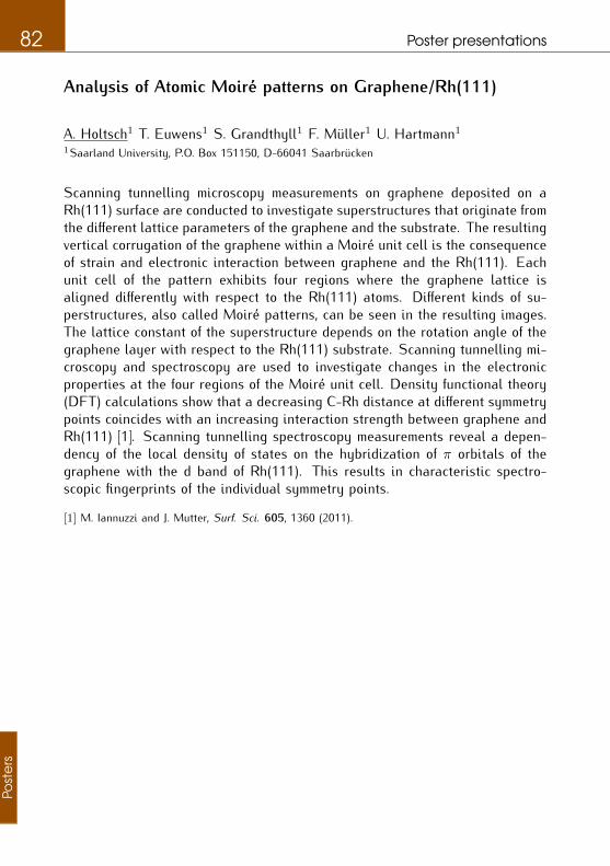
82 Poster presentations
Analysis of Atomic Moiré patterns on Graphene/Rh(111)
A. Holtsch1 T. Euwens1 S. Grandthyll1 F. Müller1 U. Hartmann1
1Saarland University, P.O. Box 151150, D-66041 Saarbrücken
Scanning tunnelling microscopy measurements on graphene deposited on aRh(111) surface are conducted to investigate superstructures that originate fromthe different lattice parameters of the graphene and the substrate. The resultingvertical corrugation of the graphene within a Moiré unit cell is the consequenceof strain and electronic interaction between graphene and the Rh(111). Eachunit cell of the pattern exhibits four regions where the graphene lattice isaligned differently with respect to the Rh(111) atoms. Different kinds of su-perstructures, also called Moiré patterns, can be seen in the resulting images.The lattice constant of the superstructure depends on the rotation angle of thegraphene layer with respect to the Rh(111) substrate. Scanning tunnelling mi-croscopy and spectroscopy are used to investigate changes in the electronicproperties at the four regions of the Moiré unit cell. Density functional theory(DFT) calculations show that a decreasing C-Rh distance at different symmetrypoints coincides with an increasing interaction strength between graphene andRh(111) [1]. Scanning tunnelling spectroscopy measurements reveal a depen-dency of the local density of states on the hybridization of π orbitals of thegraphene with the d band of Rh(111). This results in characteristic spectro-scopic fingerprints of the individual symmetry points.
[1] M. Iannuzzi and J. Mutter, Surf. Sci. 605, 1360 (2011).
Post
ers

Poster presentations 83
Mechanical and Electrical Study of 2D materials by novelDual-Probe Atomic force- /Scanning tunneling microscope
S. Hummel1 K. Elibol1 B. C. Bayer1 J. Kotakoski1 J. C. Meyer11Physics of Nanostructured Materials, University of Vienna
Scanning probe microscopy (SPM) techniques are one of the most importantexperimental methods within the field of Surface- and Nanosciences. Since onecan, in principle, obtain topographic information and spectroscopic data withatomic resolution at the same time, SPM techniques are also an invaluabletool within the relatively new field of low-dimensional materials. However, whendealing with suspended 2D materials (e.g. graphene, MoS2, etc.), interpretationof the measured data is very complicated, since the tip sample interaction isalso changing the topography of the membrane. In this work, I will show recentresults of a novel type of Dual-Probe AFM (Atomic force microscope)/STM(Scanning tunneling microscope) measurement, where the two probes approacha suspended membrane from opposite sides. Having the STM tip in tunnelingdistance to the membrane, we were able to investigate its dynamical responseas a function of the position of the cantilever of the AFM. This provides insightinto the interaction of the tip and the membrane . Additionally, we observedlocal deformations of 2D materials caused by an approaching STM tip, whileperforming AFM measurements on the same site. Furthermore, operating thedevice in STM/STM mode, we can explore electrical properties of suspendedmembranes and perform transport measurements at arbitrarily close distancesof the two probes.
Post
ers

84 Poster presentations
In-situ TEM Observation of Oxygen Vacancy Driven Structuraland Resistive Phase Transitions in La2/3Sr1/3MnO3
S. Inkinen1 L. D. Yao1 S. van Dijken1
1NanoSpin, Department of Applied Physics, Aalto University School of Science
Oxygen defects can have a profound effect on the physical properties of transi-tion metal oxides. Electric-field driven migration of oxygen vacancies providesa viable mechanism for the formation, rupture and reconstruction of conduct-ing filaments in insulating oxides, an effect that is used in nanoscale resistiveswitching devices [1,2]. In complex oxides where magnetic, ferroelectric and su-perconducting phases emerge from strong correlations between localized tran-sition metal valence electrons, oxygen vacancies can radically alter a pluralityof intrinsic properties via valence changes and structural phase transitions [3].The ability to reversibly control the concentration and profile of oxygen va-cancies in oxide nanostructures would thus open up comprehensive prospectsfor new functional ionic devices. Advancements in this direction require experi-mental techniques that allow for simultaneous measurements of oxygen vacancydynamics, atomic-scale structural effects and macroscopic physical properties.Here, we use nanoprobing in-situ transmission electron microscopy (TEM) todemonstrate reversible switching between three distinctive resistance states inan epitaxial La2/3Sr1/3MnO3 film. Simultaneous high-resolution imaging andresistance probing indicate that the switching events are caused by fast anduniform growth of new structural phases. Reversible migration of oxygen va-cancies within the manganite film and between the film and Nb-doped SrTiO3substrate, driven by combined effects of Joule heating and bias voltage, trig-gers the structural and resistive transitions. Our findings open prospects forionotronic devices based on dynamic control of physical properties in complexoxide nanostructures.
[1] R. Waser and M. Aono, Nat. Mater. 6, 833 (2007).[2] J.J. Yang, D.B. Strukov, and D.R. Stewart, Nat. Nanotech. 8, 13 (2013).[3] S. Kalinin and N.A. Spaldin, Science 341, 858 (2013).
Post
ers

Poster presentations 85
Engineering SrTiO3/LaAlO3 heterostructures thickness: an abinitio study
F. Iori11Universite’ Paris Sud - CNRS - Marie Curie fellow
The possibility to achieve conducting and superconducting properties at the in-terface between two bulk insulator oxides as SrTiO3 (STO) and LaAlO3 (LAO)in 2004 [1] has wide opened the route toward the discovery and control of broadfunctional emerging properties in different oxides heterostructures. Nonethe-less the STO/LAO system still present not clarified questions concerning thepossibility to control the presence of the 2DEG at the interface. In this work wepresent our theoretical results supported by experimental measurements con-cerning the possibility to tune the critical thickness of the LAO topmost layerthrough the deposition of a metallic capping layer at the surface. Our ab initioDensity Functional Theory calculations show how different metallic contact canlead to a reduction of the LAO critical thickness of 4 u.c. still preserving the2D electronic gas at the interface.
[1] Otomo and Hwang„ Nature 427, 423 (2004).
Post
ers

86 Poster presentations
Describing MoS2 Nanoclusters with Classical Potentials
M. J. Jäger11Aalto University, Applied Physics Department
MoS2 has recently gained research interest in various fields.This inexpensivematerial is used currently mainly as a lubricant and for the hydrodesulfurisa-tion reaction, but is gaining attention for other catalytic reactions, especiallyhydrogen evolution. Recent studies of single-layer MoS2 have shown thatits electronic band structure can be fine-tuned on the nanoscale [1]. Remark-able metallic properties occur at edges of triangularly to hexagonally shapednanoclusters which are likely to be the active site for the hydrogen evolutionreaction [1,2,3]. In this poster presentation, it will be shown how to simulateMoS2 nanoclusters with a classical Stillinger-Weber potential. Trends on elec-tronic energy and structure of MoS2 with respect to different sizes and shapeswill be presented.
[1] Sorensen et al., ACS Nano 8, 6788 (2014).[2] Bruix et al., ACS Nano 9, 9322 (2015).[3] Walton et al., J. Catal. 308, 306 (2013).
Post
ers

Poster presentations 87
Self-interaction corrected energy functionals and Pipek-Mezeyorbital localization
E. Jónsson1 M. Puska1 H. Jónsson1,2
1Department of Applied Physics, Aalto University2Faculty of Physical Sciences, University of Iceland
While Kohn-Sham density functional theory (KS-DFT) has been extremely suc-cessful and is now widely used in the studies of molecules and condensed matterit has several shortcomings. This is due to the self-interaction error (SIE) in-herent to practical implementations of the method. This, for example, makesthe description of energy levels in semi-conductors, defect states in crystals,and magnetic states of metallic nanoclusters problematic. The Perdew-Zungerself-interaction correction (PZ-SIC) [1] implemented in a fully variational andself-consistent way using complex orbitals [2] has recently been found to besuccessful where commonly used exchange-correlation functionals fail. Accu-rate band-gap estimates for semi-conductors and insulators have been obtainedwhich are in good agreement with GW calculations [3]. Furthermore, PZ-SICcalculations of localized defect states in crystals [4], charge-localized states inmolecules [5] and magnetic states of metallic n anoclusters have been found tobe in good agreement with experimental results while even hybrid functionalKS-DFT calculations were in error.
The set of orbitals produced by conventional KS-DFT calculations (canon-ical orbitals, COs) typically extend over the whole system, making the analysisof the bonding and geometrical arrangement of atoms difficult. By defining aunitary rotation on the set of COs to produce localized orbitals (LOs) the prop-erties of the system stay the same, but chemical bonding and geometry can bemore readily rationalized. Recently [2] a generalization of the Pipek Mezeyorbital localization was presented and shown to produce a clear separation ofσ and π type orbitals while being a simple and an efficient post processing tool.This method has been extended to the condensed matter case where it is shownto produce as localized orbitals as the maximally localized Wannier functions(MLWFs), while maintaining clear σ and π bond separation and hence con-forms to chemical intuition [5], while MLWFs produce mixed bonding orbitals(’banana’-shaped).
[1] J. P. Perdew and A. Zunger, Phys. Rev. B 23, 5048 (1981).[2] S. Lehtola and H. Jónsson, J. Chem. Theory Comput. 10, 5324 (2014).[3] E. ó. Jónsson, P. Rinke, M. Puska and H. Jónsson, (in preparation) . (2017).[4] H. Gudmundsdóttir, E. Ö. Jónsson and H. Jónsson, N. J. Phys. 17, 083006 (2015).[5] X. Cheng, Y. Zhang, E. Ö. Jónsson, H. Jónsson and P. M. Weber, Nat. Commun. 7, .11013
(2016). Post
ers

88 Poster presentations
[6] E. ó. Jónsson, S. Lehtola, M. Puska and H. Jónsson, J. Chem. Theory Comput. accepted forpublication, . (2016).
[7] S. Lehtola and H. Jónsson, J. Chem. Theory Comput. 10, 642 (2014).
Post
ers

Poster presentations 89
Local Electronic Structure of a Magnetic Dimer Impurity in aSuperconductor
S. Kezilebieke1 M. Dvorak2 T. Ojanen3 P. Rinke2 P. Liljeroth1
1Department of Applied Physics, Aalto University School of Science, P.O.Box 15100, 00076Aalto, Finland
2Department of Applied Physics, Computational Electronic Structure Theory3Department of applied physics (Low Temperature Laboratory) Aalto University, Finland
Magnetic impurities have a dramatic effect on superconductivity by breakingthe time-reversal symmetry and inducing low energy bound states within thesuperconducting gap[1-3]. More interestingly, coupling between the individualmagnetic impurities and superconducting substrate is essential for the forma-tion of Majorana modes which have been detected in ferromagnetic chains of Featoms on a Pb(110) surface[4]. Therefore, it is important to have a fundamen-tal understanding of the low energy bound states, their spatial extension, andthe coupling between such states. Here, we demonstrate how a single cobaltphthalocyanine (CoPC) molecule modifies 2D superconducting states and thebound state within the gap extends spatially over nanometer from its magneticcenter. The spatially extended states allow us to study the magnetic couplingbetween the impurities using a low-temperature scanning tunneling microscopyand spectroscopy. Our experimental work is supported by theo retical estimatesof the coupling between magnetic impurities on the 2D superconductor. Thiswork provides fundamental understanding of coupled bound states, which formthe basis of the proposed exotic quantum states such as topological supercon-ductivity in 2D magnetic lattices. These phenomena in artificial materials willallow the design and fabrication of new topological quantum devices.
[1] Hiroyuki Shiba, Progress of Theoretical Physics 40, 435 (1968).[2] YU LUH, Acta Physica Sinica 21, 75 (1965).[3] A.I. Rusinov, Sov. Phys.JETP 29, 11016 (1969).[4] Stevan Nadj-Perge, Ilya K. Drozdov, Jian Li, Hua Chen, Sangjun Jeon, Jungpil Seo, Allan H.
MacDonald, B. Andrei Bernevig, and Ali Yazdani, Science 346, 602 (2014).
Post
ers
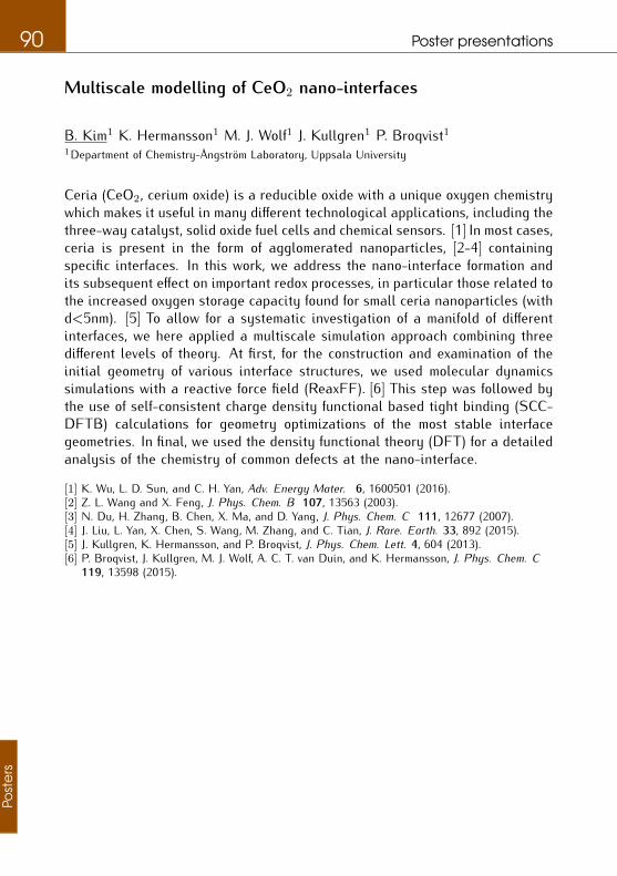
90 Poster presentations
Multiscale modelling of CeO2 nano-interfaces
B. Kim1 K. Hermansson1 M. J. Wolf1 J. Kullgren1 P. Broqvist11Department of Chemistry-Ångström Laboratory, Uppsala University
Ceria (CeO2, cerium oxide) is a reducible oxide with a unique oxygen chemistrywhich makes it useful in many different technological applications, including thethree-way catalyst, solid oxide fuel cells and chemical sensors. [1] In most cases,ceria is present in the form of agglomerated nanoparticles, [2-4] containingspecific interfaces. In this work, we address the nano-interface formation andits subsequent effect on important redox processes, in particular those related tothe increased oxygen storage capacity found for small ceria nanoparticles (withd<5nm). [5] To allow for a systematic investigation of a manifold of differentinterfaces, we here applied a multiscale simulation approach combining threedifferent levels of theory. At first, for the construction and examination of theinitial geometry of various interface structures, we used molecular dynamicssimulations with a reactive force field (ReaxFF). [6] This step was followed bythe use of self-consistent charge density functional based tight binding (SCC-DFTB) calculations for geometry optimizations of the most stable interfacegeometries. In final, we used the density functional theory (DFT) for a detailedanalysis of the chemistry of common defects at the nano-interface.
[1] K. Wu, L. D. Sun, and C. H. Yan, Adv. Energy Mater. 6, 1600501 (2016).[2] Z. L. Wang and X. Feng, J. Phys. Chem. B 107, 13563 (2003).[3] N. Du, H. Zhang, B. Chen, X. Ma, and D. Yang, J. Phys. Chem. C 111, 12677 (2007).[4] J. Liu, L. Yan, X. Chen, S. Wang, M. Zhang, and C. Tian, J. Rare. Earth. 33, 892 (2015).[5] J. Kullgren, K. Hermansson, and P. Broqvist, J. Phys. Chem. Lett. 4, 604 (2013).[6] P. Broqvist, J. Kullgren, M. J. Wolf, A. C. T. van Duin, and K. Hermansson, J. Phys. Chem. C
119, 13598 (2015).
Post
ers

Poster presentations 91
Formation of hexagonal gold nanostructures duringself-assembling on Ge(001) surface
F. Krok1 B. R. Jany1 N. Gauquelin1 M. Nikiel1 T. Wilhammar1 K. van denBos1 A. Janas1 K. Szajna1 J. Verbeeck1 G. van Tendeloo11Institute of Physics Jagiellonian University2EMAT, University of Antwerp
Nano sized gold has become an important material in various fields of scienceand technology such as nanoelectronics, catalysis, nanophotonics and medicine,where control over the size and crystallography of the structures is desired totailor the functionality. The hexagonal closed packed (hcp) structure of goldis a very unusual form only recently chemically synthesized by Huang et al.[1] in form of graphene-supported thin sheets and nanowires of a few nm inthickness [2] and theoretically studied by Wang et al. [3]. The understanding ofelectrical as well as physical properties of the system is of great importance andstrongly linked to their atomic structure. In the presentation, we will report onthermally-induced nanostructures formation after deposition of thin film of Au onreconstructed Ge(001) in UHV. It has been found that there exists preferentialAu island orientation along crystallographic direction of the substrate surfaceas provided by diffraction methods (EBSD). For an annealing temperature closeto the eutectic temperature of Au/Ge system (640 K), change in size and shapeof the Au nanoislands is observed as well as the apparition of the hexagonalphase of gold, indicating eutectic melting of the system. TEM measurements ofAu/Ge(001) sample cross sections revealed that the nanoislands created uponannealing at T<640 K are on top of the Ge(001) surface, while for T>640 K partof the island is buried beneath the substrate surface, which confirms the eutecticAuGe melting. The chemical composition of the Au/Ge interface was uncoveredusing quantitative atomically resolved HAADF-STEM and indicate the absenceof alloyin g. The crystallographic structure of the Au islands and the presenceof hexagonal gold as well as the Au/Ge interface were studied by quantitativeatomically resolved HAADF-STEM and their structure was determined.
[1] Huang, X., et al., Nat. Commun. 2, 292 (2011).[2] Fan, Z., et al., Nat. Commun. 6, 372 (2015).[3] Wang, C., et al., Scientific Reports 5, 10213 (2015).
Post
ers

92 Poster presentations
Theoretical Prediction of One-Atom-Thick Hexagonal CrN:Electronic Structure and Magnetic Properties
A. V. Kuklin1,2 A. A. Kuzubov2 S. A. Shostak2 P. V. Avramov11Department of chemistry, Kyungpook National University, 80 Daekharo, Bukgu, Daegu, 41556,South Korea
2Siberian Federal University, 79 Svobodny pr., Krasnoyarsk, 660041, Russia
The family of 2D materials is rapidly increasing since the discovery of graphene[1]. Each new material brings interesting properties, which are usually differentfrom their bulk analogues. Many theoretically predicted 2D materials with hon-eycomb structure, which are non-layered in bulk, were confirmed in experimen-tal reports where graphitic thin ZnO [2], GaN [3] and stanene [4] were fabricatedthrough different experimental techniques. Thin films of transition metal nitrides(TMNs) may provide one more possibility to obtain low-dimensional materialswith unique spin-related properties because unpaired d-electrons are respon-sible for the formation of spin-depended surface electronic states. Transitionmetal mononitrides are known as advantage class of compounds. They have,relatively, high hardness, melting point, interesting optical, electronic, catalytic,and magnetic properties. In contrast to the most of one-atom thick 2D latticeslike graphene, h-BN, transition metals dichalcogenides, etc. the TMN monolay-ers might be magnetic due to the presence of unpaired d-electrons. Therefore,no magnetic substrates or no doping with any atoms is necessary to inducespin injection into low-dimensional non-magnetic fragments for spin-relatedapplications [5,6]. Using first principle calculations, we predict the existence ofgraphene-like hexagonal chromium nitride (h-CrN) with almost flat atomicallythin structure. The results of the geometry search and phonon calculation ofh-CrN indicate the possibility to create a 2D chromium nitride monolayer of(111) crystallographic orientation. The electronic structure calculations revealthat freestanding h-CrN has 100% spin-polarized half-metallic nature with pos-sible ferromagnetic ordering. At HSE06 hybrid functional level of theory, theDOS of h-CrN displays the similar shape with the same band gap of spin-down(3.9 eV). As a possible way to stabilization and synthesis, deposition of h-CrNon 2D MoSe2 or on MoS2 is designed due to the quite good match of theircrystalline lattice with h-CrN. The formation of composites keeps half-metallicproperties and leads to reducing of spin-down band gaps up to 1.43 and 1.71eV for energetically favorable h-CrN/MoSe2 and h-CrN/MoS2 configurations,respectively. It was also found that the electronic density at the Fermi levelof h-CrN/MoS2 heterostructure is much higher one of the freestanding h-CrNsheet. The h-CrN may be considered as a potential new fundamental 2D ma-terial with promising magnetic properties.Po
ste
rs

Poster presentations 93
Authors acknowledge the Siberian Supercomputer Center (SSCC) of SBRAS, Novosibirsk; the Institute of Computational Modeling of SB RAS, Kras-noyarsk; the Joint Supercomputer Center of RAS, Moscow and the ICC ofNovosibirsk State University for providing the computing resources. This workwas supported by the government contract of the Ministry of Education andScience of the Russian Federation to Siberian Federal University (Grant No.16.1500.2014/K). A.V.K. acknowledges BK21 fund.
Post
ers

94 Poster presentations
A general computational method for electron emission andthermal effects in field emitting nanotips
A. Kyritsakis1,2 F. Djurabekova1,2
1Deparment of Physics, University of Helsinki, PO Box 43 (Pietari Kalmin katu 2), 00014Helsinki, Finland
2Helsinki Institute of Physics, Helsinki, Finland
Electron emission from nanometric size emitters becomes of increasing inter-est due to its involvement to sharp electron sources, carbon nanotubes, vac-uum breakdown phenomena and various other vacuum nanoelectronics applica-tions. The most commonly used theoretical tools for the calculation of electronemission are still nowadays the Fowler-Nordheim and the Richardson-Laue-Dushman equations although it has been shown since the 1990’s that they areinadequate for nanometrically sharp emitters or in the intermediate thermal-field regime.
In this paper we develop a computational method for the calculation of emis-sion currents and Nottingham heat, which automatically distinguishes amongdifferent emission regimes, and implements the appropriate calculation methodfor each. Our method covers all electron emission regimes (thermal, field andintermediate), aiming to maximize the calculation accuracy while minimizing thecomputational time.
As an example, we implemented it in atomistic simulations of the ther-mal evolution of Cu nanotips under strong electric fields and found that thepredicted behaviour of such nanotips by the developed technique differs sig-nificantly from estimations obtained based on the Fowler-Nordheim equation.Finally, we show that our tool can be also successfully applied in the analysisof experimental current-voltage data.
Our method has been implemented in an open-source computational tool,which is publicly available in https://github.com/AndKyr/GETELEC/. This toolcan be used for either fast and simple calculation of emission currents or as alibrary for complex simulations of phenomena that involve electron emission.
Post
ers

Poster presentations 95
MHDA-Functionalized carbon nanotubes for detectingnon-aromatic VOCs and warfare agents
A. Thamri1 H. Baccar1 C. Struzzi1 C. Bittencourt1 A. Abdelghani1 E. Llobet11Carthage University, National Institute of Applied Science and Technology, Bp676, 1080Charguia Cedex, Tunisa
2Plasma-Surface Interaction Chemistry University of Mons, 1 Copernic, 7000 Mons, Belgium.3MINOS-EMaS, Universitat Rovira i Virgili, Avda. Paisos Catalans, 26, 43007 Tarragona, Spain
The chemical modification of multiwalled carbon nanotubes (MWCNTs)is re-ported as a way to improve sensitivity and response time of gas sensors for de-tecting alcohols, acetone and warfare agents simulants such as DMMP [1,2]. Wehave developed sensors employing MWCNTs decorated with gold nanoparticlesand modified with a 16-mercaptohexadecanoic acid (MHDA) monolayer. Mor-phological and compositional analysis by Transmission Electron Microscopy(TEM), Fourier Transform Infra-red Spectroscopy (FTIR) and X-ray photoelec-tron spectroscopy were performed to characterize the gold nanoparticles and tocheck the bonding of the thiol monolayer. The detection of aromatic and non-aromatic volatiles and DMMP vapors by MWCNT/Au and MWCNT/Au/MHDAshows that the presence of the self-assembled layer increases sensitivity andselectivity towards nonaromatics. Furthermore, it ameliorates response dynam-ics, and significantly reduces nitrogen dioxide and moisture cross-sensitivity.
[1] Clement, P. et al. , Adv. Func. Mat. 25, 4011 (2015).[2] A. Thamri et al., Sci. Rep. 6, 35130 (2016).
Post
ers

96 Poster presentations
Nanoripples production on a-Si surfaces under Ar irradiation
A. Lopez-Cazalilla1 A. ILinov1 L. Bukonte1 J. Perkinson2 M. Aziz2 S. Norris3F. Djurabekova1 K. Nordlund1
1Department of Physics, P.O. 43, FI-00014 University of Helsinki, Finland2Harvard School of Engineering and Applied Sciences, Cambridge, Massachusetts, 02138, USA3Department of Mathematics, Southern Methodist University, Dallas, Texas 75205, USA
Ion beams are frequently used in industry for composition control of differentmaterials as well as thin film deposition. It was noticed that low- and medium-energy ions at high fluencies produce nanoripples and quantum dots on theirradiated surfaces. In the present work we focus our attention on the studyof irradiation of amorphous silicon (a-Si) and germanium (a-Ge) with 1 keV Arions under different angles, taking into special consideration the angles closeto grazing incidence.
This study has been carried out with Molecular Dynamics (MD), measuringthe stress generated in the simulation cell as well as the total displacementof the particles which compound the cell, following the previous work on thismatter [1]. The MD results are subsequently fed into a numerical module thatallows the prediction of the ripple wavelength, which can be directly comparedwith experimental observations.
[1] Scott Norris, Juha Samela, Laura Bukonte, Marie Backman, Flyura Djurabekova, KaiNordlund, Charbel S. Madi, Michael P. Brenner and Michael Aziz, Nature Communications 2,276 (2011).
Post
ers

Poster presentations 97
Straining free-standing 2D materials in a TEM
U. Ludacka1 M. Tripathi1 T. Susi1 C. Rentenberger1 J. Kotakoski11Faculty of Physics, University of Vienna
During the last decade, research on two-dimensional (2D) materials, epitomizedby graphene and MoS2, has spawned a number of suggested applications in-cluding stretchable electronics. Theoretical calculations have shown a maximumstrain for graphene up to 20% and about 10% for MoS2. However, measuringthe intrinsic properties of 2D materials is difficult due to their delicacy.
We demonstrate here a simple method to strain freestanding 2D materialsin situ in a transmission electron microscope (TEM). Our graphene and MoS2
samples are grown through chemical vapor deposition and suspended on asubstrate of perforated carbon films on gold TEM grids. The grids are gluedonto a stretching holder and strained with small incremental steps to avoidbreaking the membrane during the experiment.
We measure the deformation of the membranes from the diffraction patternat each step. The change in the position of the diffraction spots allows usto estimate the applied uniaxial strain and to calculate the Poisson’s ratio forboth materials. Until now, the maximum uniaxial strain we have reached isapproximately 1.5% - at larger strains the support film breaks. This problemmay be overcome by using different substrates.
At higher strains our technique should allow the direct study of crack for-mation and propagation at the atomic level. These can then be correlated withthe grain boundaries and their junctions in polycrystalline samples. Moreover,strain is also expected to have an influence on the formation and migrationof point defects, which we can introduce with the electron beam during theexperiment.Po
ste
rs

98 Poster presentations
Molybdenum carbide and superconducting nitride nanowires:facile synthesis, transport measurements and their use astransparent electrodes
A. Mrzel1 D. Vengust1 J. Buh1 J. Ravnik1 M. Vilfan1 V. Kabanov1D. Mihailovic11Jozef Stefan Institute, Jamova cesta 39, SI-1000 Ljubljana, Slovenia
We demonstrate a new and effective method of producing gram quantities ofmolybdenum carbide [1] and single-phase superconducting δ-MoN nanowires[2] from bundled Mo6SyIz (8.2 ≤ y + z ≤ 10) nanowire templates in the pres-ence of mixture of hydrogen/ethane and ammonia gas, respectively. By con-trolling the reaction conditions during the carburization, we can modify theratio between MoC and Mo2C carbide phases in nanowires and produce anew hybrid inorganic/organic nanomaterial composed of molybdenum carbidenanowires densely covered with carbon nanofibres. We used the same approachon nanowire networks and demonstrate a new use of molybdenum carbide andnitride in the form of nanowire networks as transparent electrodes. The sheetresistance of such robust and air-stable electrodes is around 1000 Ω/sq atroom temperature and their optical transmittance between 93 % and 95 % inthe range of 200 − 900 nm. The electrodes are thus suitable for electro-opticapplications, especially where high transparency in the UV region is required.Measurements of four-contact resistance on single molybdenum nitride wireswith diameters above 100 nm in a magnetic field are used to determine the criti-cal field. We show that switching between different metastable superconductingstates in δ-MoN nanowires can be very effectively manipulated by introduc-ing small amplitude electrical noise. Furthermore, we show that deterministicswitching between metastable superconducting states with different numbersof phase-slip centres can be achieved in both directions with small electricalcurrent pulse perturbations of appropriate polarity [3].
[1] D. Vengust, J. Ravnik, A. Mrzel, M. Vilfan, RSC Adv. 6, 90806 (2016).[2] J. Buh, A. Kovic, A. Mrzel, Z. Jaglicic, A. Jesih, D. Mihailovic, Nanotech 25, 025601 (2014).[3] J. Buh, V. Kabanov, V. Baranov, A. Mrzel, A. Kovic, D. Mihailovic, Nat. Comm. 6, 10250 (2015).
Post
ers

Poster presentations 99
Buckyball Sandwiches
K. Mustonen1 R. Mirzayev1 M. Monazam1 A. Mittelberger1 T. J. Pennycook1C. Mangler1 T. Susi1 J. Kotakoski1 J. C. Meyer11Physics of Nanostructured Materials, University of Vienna
Two-dimensional (2D) materials have considerably expanded the field of ma-terials science in the last decade. Very recently various 2D materials havebeen assembled into vertical van der Waals heterostacks, and it has also beenproposed to combine them with other low- dimensional structures to create newmaterials with possibly hybridized properties. In this contribution we demon-strate the first direct images of a suspended 0D/2D heterostructure incorpo-rating C60 molecules between two graphene layers in a buckyball sandwichstructure [1]. We demonstrate clean and ordered C60 islands with thicknessesdown to one molecule, shielded by the graphene layers from the microscopevacuum and partially protected from radiation damage during scanning trans-mission electron microscopy imaging. The demonstrated sandwich structureserves as a 2D nanoscale reaction chamber allowing the molecular structureand dynamics to be analyzed at atomic resolution.
[1] R. Mirzayev , K. Mustonen, M.R.A. Monazam, A. Mittelberger, T.J. Pennycook, C. Mangler, T.Susi, J. Kotakoski and J.C. Meyer, Submitted 1, 1 (2016).
Post
ers
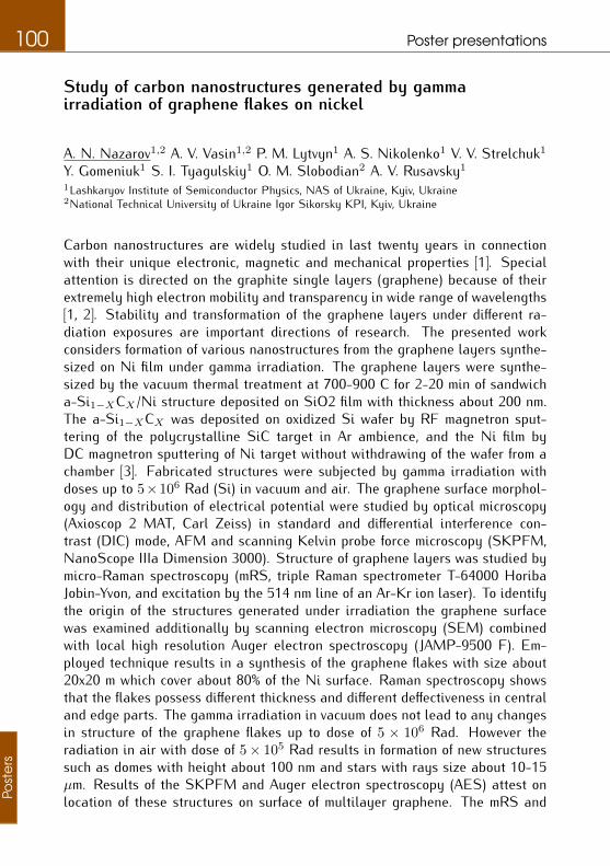
100 Poster presentations
Study of carbon nanostructures generated by gammairradiation of graphene flakes on nickel
A. N. Nazarov1,2 A. V. Vasin1,2 P. M. Lytvyn1 A. S. Nikolenko1 V. V. Strelchuk1Y. Gomeniuk1 S. I. Tyagulskiy1 O. M. Slobodian2 A. V. Rusavsky1
1Lashkaryov Institute of Semiconductor Physics, NAS of Ukraine, Kyiv, Ukraine2National Technical University of Ukraine Igor Sikorsky KPI, Kyiv, Ukraine
Carbon nanostructures are widely studied in last twenty years in connectionwith their unique electronic, magnetic and mechanical properties [1]. Specialattention is directed on the graphite single layers (graphene) because of theirextremely high electron mobility and transparency in wide range of wavelengths[1, 2]. Stability and transformation of the graphene layers under different ra-diation exposures are important directions of research. The presented workconsiders formation of various nanostructures from the graphene layers synthe-sized on Ni film under gamma irradiation. The graphene layers were synthe-sized by the vacuum thermal treatment at 700-900 C for 2-20 min of sandwicha-Si1−XCX /Ni structure deposited on SiO2 film with thickness about 200 nm.The a-Si1−XCX was deposited on oxidized Si wafer by RF magnetron sput-tering of the polycrystalline SiC target in Ar ambience, and the Ni film byDC magnetron sputtering of Ni target without withdrawing of the wafer from achamber [3]. Fabricated structures were subjected by gamma irradiation withdoses up to 5×10⁶ Rad (Si) in vacuum and air. The graphene surface morphol-ogy and distribution of electrical potential were studied by optical microscopy(Axioscop 2 MAT, Carl Zeiss) in standard and differential interference con-trast (DIC) mode, AFM and scanning Kelvin probe force microscopy (SKPFM,NanoScope IIIa Dimension 3000). Structure of graphene layers was studied bymicro-Raman spectroscopy (mRS, triple Raman spectrometer T-64000 HoribaJobin-Yvon, and excitation by the 514 nm line of an Ar-Kr ion laser). To identifythe origin of the structures generated under irradiation the graphene surfacewas examined additionally by scanning electron microscopy (SEM) combinedwith local high resolution Auger electron spectroscopy (JAMP-9500 F). Em-ployed technique results in a synthesis of the graphene flakes with size about20x20 m which cover about 80% of the Ni surface. Raman spectroscopy showsthat the flakes possess different thickness and different deffectiveness in centraland edge parts. The gamma irradiation in vacuum does not lead to any changesin structure of the graphene flakes up to dose of 5 × 10⁶ Rad. However theradiation in air with dose of 5× 10⁵ Rad results in formation of new structuressuch as domes with height about 100 nm and stars with rays size about 10-15µm. Results of the SKPFM and Auger electron spectroscopy (AES) attest onlocation of these structures on surface of multilayer graphene. The mRS andPo
ste
rs

Poster presentations 101
AES show that the structures compose of carbon. The rays are probably carbontubes with diameters about 100-120 nm. The domes have a surface potentialconsiderable lower than graphene layer that assumes either formation strainedgraphene structure or incorpo ration in the graphene layer any inclusions inthese places. Also doublet behavior of Raman G band is observed for scanningof the dome structures that can be explained by strained layers formation dur-ing the gamma-irradiation of the graphene flakes. A nature of synthesis of suchcarbon structures under the irradiation is discussed.
[1] K.S. Novoselov, A.K. Geim, S.V. Morozov, D. Jiang, Y. Zhang, S.V. Dubonos, I.V. Grigorieva, andA.A. Firsov„ Science 306, 666 (2004).
[2] T.H. Seo, K.J. Lee, A.H. Park, C.-H. Hong, E.-K. Suh, S.J. Chae, Y.H. Lee, T.V. Cuong, V.H.Pham, J.S. Chung, E.J. Kim, and S.-R. Jeon„ Opt. Exp. 19, 23111 (2011).
[3] A.N. Nazarov, S.O. Gordienko, P.M. Lytvyn, V.V. Strelchuk, A.S. Nikolenko, A.V. Vasin, A.V.Rusavsky, V.S. Lysenko, and V.P. Popov„ Phys. Stat. Sol. (c) 10, 1173 (2013).
Post
ers

102 Poster presentations
Graphene processing towards applications
M. Quintana1
1Instituto de Fisica, Universidad Autonoma de San Luis Potos
Several methods have been established for graphene preparation. However,most of them remain as demonstration techniques, mainly for basic research,and for providing proof of concept devices. Instead, the recent progress in mak-ing stable graphene dispersions allows the production of graphene sheets ona more preparative scale and permits the manipulation of the layers by chem-ical reactions. Thus, chemically manipulated graphene samples can be easilyincorporated into new functional materials or can be modified for the forma-tion of other carbon nanostructures. In this work, I will show our recent effortstoward 1) producing graphene stable dispersions [1]; 2) ultrasonic approachesperformed in graphene dispersions that modify its chemical [2], and structuralproperties [3,4], i.e. MWNTs production by rolling up a graphene sheet; andfinally 3) an applications where functionalized graphenes are used for photo-dynamic therapy [5].
[1] M. Quintana, M. Grzelczak, K. Spyrou, S. Baals, B. Kooi, G. Van Tendeloo, P. Rudolf, M.Prato, Chem. Commun. 48, 12159 (2012).
[2] M. Quintana, E. Vazquez, M. Prato, Acc. Chem. Res. 46, 138 (2013).[3] M. Quintana, M. Grzelczak, K. Spyrou, M. Calvaresi, S. Baals, B. Kooi, G. Van Tendeloo, P.
Rudolf, F. Zerbeto, M. Prato, J. Am. Chem. Soc. 134, 13310 (2012).[4] J. I. Tapia, E. Larios, C. Bittencourt, M.J. Yacamn, M. Quintana, Carbon 99, 541 (2016).[5] D. Hernandez-Sanchez, M. Scardamaglia, S. Saucedo-Anaya, C. Bittencourt, M. Quintana,
RCS Advances 6, 66634 (2016).
Post
ers

Poster presentations 103
First principles training sets and atomistic potentials forboron-nitride nanostructures
I. Tamblyn1,2
1National Research Council of Canada2Department of Physics, University of Ontario Institute of Technology
Boron nitride nanotubes are a promising material for nanoscale reinforcementof composites. An analog of the more familiar carbon nanotube family, boronnitride nanotubes exhibit exceptional structural, mechanical, and thermal prop-erties. They are optically transparent and have high thermal stability, sug-gesting a wide range of opportunities for structural reinforcement of materialsincluding glass, ceramics, and metals.
Theoretical modeling can play an important role in determining the optimalapproach to integrating nanotubes into a supporting matrix. The most promisingcomposites (with respect to mechanical load transfer) involve covalent function-alization of the supporting nanotubes. Developing accurate, atomistic scalemodels of such nanoscale interfaces embedded within composites is challeng-ing, however, due to the mismatch of length scales involved. Typical nanotubediameters range from 5-50 nm, with a length as large as a micron (i.e. a relevantlengthscale for structural reinforcement). Unlike their carbon-based counter-parts, well tested and transferable interatomic force fields are not common forBNNT. In light of this, we have developed an extensive training database ofBN rich materials, under conditions relevant for BNNT synthesis and compos-ites based on extensive first principles molecular dynamics simulations. Usingthis data, we have produced an artificial neural network poten tial capable ofreproducing the accuracy of first principles data at significantly reduced compu-tational cost, allowing for accurate simulation at the much larger length scalesneeded for composite design.Po
ste
rs

104 Poster presentations
Carbon-vacancy complexes controlling nano-scale irradiationdamage in iron and steels
D. Terentyev11SCK-CEN, Belgian Nuclear Research Centre, Boeretang 200, Mol, Belgium
Ab initio techniques was applied to compute energetic stability of Carbon-vacancy complexes and positron life time in BCC Fe. Positron lifetime isfound to be tremendously sensitive to local Carbon-vacancy, Carbon-Carbonand vacancy-vacancy arrangements. Depending on C-V multiplicity, a certaincomplex is indistinguishable or to be detected as a single or clusterized vacancyby positron annihilation spectroscopy. Combining ab intio database for the lifetime and energetics of C-V clusters, rate theory cluster dynamics calculationswere performed to model annealing of Fe-C alloys after electron irradiationin the conditions identical to experiment. Analysis of the lifetime spectrumand results of rate theory calculations allows one to qualitatively explain andaccurately reproduce the experimental data if di-Carbon-vacancy complex isconsidered to be mobile. The migration energy of 1.1 eV is drawn from the bestfit to experimental data.
Post
ers

Poster presentations 105
Conversion of light for the production of fuels using cellfactories
J. Selin1 J. Pitkänen2 V. Pale1,2 C. Tossi1 P. Blomberg2 J. Jäntti2 M. Penttila2
I. Tittonen1
1Department of Micro- and Nanosciences, School of Electrical Engineering, Aalto University,Finland
2VTT Technical Research Centre, Finland
Sunlight can promote water electrolysis in order to obtain hydrogen gas, whichin turn can be paired with CO2 to produce hydrocarbons. Phototrophic mi-crobes, instead, can combine light and carbon dioxide in a wide range of organiccompounds with a high product selectivity but exploiting only a small portionof the solar spectrum[1][2]. A third and interesting combination is microbialelectrosynthesis, the capture of sunlight-generated electrons by microbes inorder to drive the conversion of carbon dioxide to organic compounds[3]. Thecritical points in this type of processes are the low reactivity of CO2, productselectivity, poor interaction between the electrical and biological components,and finally the necessity to tailor which fractions of the solar spectrum willbe used by the device: UV light can be harmful to microbes, and some wave-lengths might need to be converted in order to exploit as much light as possible.We aim to overcome these limitations by creating new optoelectronic nanotechmaterials (using nanostructured III-V semiconductors and plasmonic nanopar-ticles), engineering new microbial species, and finding a way to interface thetwo systems. A similar scope is being successfully pursued by a research teamin Harvard, where CO2 reduction and water electrolysis were achieved thanksto the interface between a biocompatible electrode and a strain of RalstoniaEutropha[4].
[1] J. Qiao, Y. Liu, F. Hong, J. Zhang, Chem. Soc. Rev. 43, 631 (2014).[2] K. M. Weyer, D. R. Bush, A. Darzins, B. D. Willson, BioEnergy Research 3, 204 (2010).[3] D. R. Lovley, K. P. Nevin, Current Opinion in Biotechnology 24, 385 (2013).[4] C. Liu, and B. C. Colon, M. Ziesack, P. A. Silver, D. G. Nocera, Science 352, 1210 (2016).
Post
ers

106 Poster presentations
Creating nanoporous graphene with swift heavy ions
H. Vazquez1 E. H. Åhlgren1,2 O. Ochedowski3 A. A. Leino1 R. Mirzayev4R. Kozubek3 H. Lebius6 M. Karlusic7 M. Jaksic7 A. V. Krasheninnikov5,8,9J. Kotakoski4 M. Schleberger3 K. Nordlund1 F. Djurabekova1
1Department of Physics, University of Helsinki, P.O. Box 43, 00014 Helsinki, Finland2School of Chemistry, University of Nottingham, University Park, Nottingham NG7 2RD, UnitedKingdom
3Fakultät für Physik and CENIDE, Universität Duisburg-Essen, 47048 Duisburg, Germany4Fakultät für Physik, Universität Wien, Boltzmanngasse 5, 1090 Vienna, Austria5Department of Applied Physics, Aalto University, P.O. Box 1100, 00076 Helsinki, Finland6CIMAP, (CEA-CNRS-ENSICAEN-UCN), blvd Henri Becquerel, 14070 Caen, France7Ruder Boskovic Institute, Bijenicka cesta 54, 10000 Zagreb, Croatia8Helmholtz-Zentrum Dresden-Rossendorf, Institute of Ion Beam Physics and Materials Research,01328 Dresden, Germany
9National University of Science and Technology MISiS, 4 Leninskiy prospekt, Moscow, 119049,Russian Federation
We examine swift heavy ion-induced defect production in suspended singlelayer graphene using Raman spectroscopy and a two temperature moleculardynamics model that couples the ionic and electronic subsystems. We show thatan increase in the electronic stopping power of the ion results in an increase inthe size of the pore-type defects, with a defect formation threshold at 1.22-1.48keV/layer. We also report calculations of the specific electronic heat capacity ofgraphene with different chemical potentials and discuss the electronic thermalconductivity of graphene at high electronic temperatures, suggesting a value inthe range of 1 Wm −11 K −11 . These results indicate that swift heavy ionscan create nanopores in graphene, and that their size can be tuned between1-4 nm diameter by choosing a suitable stopping power.
Post
ers

Poster presentations 107
Controlling Josephson current with topological states in bilayergraphene
D. Visontai1 P. Rakyta1 A. Kormanyos21Department of Physics of Complex Systems,Eötvös University, H-1117 Budapest, PazmanyPeter setany 1/A, Hungary
2Department of Physics, University of Konstanz, D-78464 Konstanz, Germany
We present a numerical, tight-binding calculation of dc Josephson current inlong bilayer graphene (BG) junction using four, parallel doping gates (two belowand two above the scattering region) with superconducting electrodes. As itwas shown experimentally by Li et al[1]. this setup is suitable to electronicallycontrol the band gap and generate a topological state TS in the low energyregime of BG. In our calculations we show that in case the TS extends in thewhole width of the system it couples the edge states from the opposite sides,which causes the electrons to scatter and the current to decrease. The presenceof the TS lowers the critical current by an order of magnitude and the current-phi relation is clearly distinguishable from the setup where there is no TS. Thisbehavior can be clearly observed in all the samples, which are wide enough sothat the wavefunctions of edge states do not overlap. We investigate also therobustness of this effect against disorder and magnetic field. The Josephsoncurrent is calculated by the EQUUS code, developed by the Eötvös QuantumTransport Group [2]
[1] J. Li, K. Wang, K. J. McFaul, Z. Zern, Y. Ren, K. Watanabe, T. Taniguchi, Z. Qiao & J. Zhu,Nature Nanotechnology 158, 1748-3395 (2016).
[2] P. Rakyta, A. Kormanyos, J. Cserti, Phys. Rev. B 93, 224510 (2016).
Post
ers

108 Poster presentations
In-Situ Transmission Electron Microscopy of FunctionalMaterials
L. D. Yao1 S. Inkinen1 S. van Dijken1
1NanoSpin,Department of Applied Physics, Aalto University School of Science, P.O. Box 15100,FI-00076 Aalto, Finland
One of most exciting developments in nanomaterials characterization is thecommercialization of aberration corrected TEMs and STEMs [1,2]. By correct-ing for spherical aberrations, these techniques allow for the imaging of atomicpositions with a precision of a few picometers. Together with the integrationof energy dispersive X-ray spectroscopy (EDS) and electron energy loss spec-troscopy (EELS), the structural and elemental composition of nanomaterials canbe determined at the atomic level. Recently, another exciting development inTEM has emerged, namely the use of special specimen holders for in-situ TEMmeasurements under various heating, cooling, and electrical bias conditions [3].The combination of in-situ TEM/STEM imaging and EDS/EELS analysis isextremely powerful as it allows for real-time studies on nanoscale dynamicalprocesses and their direct impact on macroscopic material properties. In theNanomicroscopy Center at Aalto University, we have established a new platformfor in-situ TEM characterization. Here, we review some recent experimental re-sults, including (1) the observation of electron beam-induced structural phasetransitions in epitaxial manganite films [4], (2) in-situ spectroscopy of electric-field controlled oxygen ion migration in metal/oxide heterostructures [5], and (3)simultaneous real-time analysis of resistive and structural phase transitions incomplex oxide nanostructures. We also present an outlook on the developmentof a combined optical/electrical probing holder for in-situ TEM measurementson perovskite solar cells. The new setup will be used to address reliabilityand durability issues of this promising new type of solar cell by simultaneouscharacterization of ion migration, ionic polarization, ferroelectricity, etc., at highspatial resolution. Realization of this measurement technique will be a majorstep in the field of in-situ TEM with direct implications for the developmentof perovskite sola r cells and other opto-electronic devices. The project is fi-nancially supported by the Key Project Funding by the Academy of Finland,2016.[1] C. L. Jia, M. Lentzen and K. Urban, Science 299, 870 (2003).[2] Jannik C. Meyer, C.O. Girit, M.F. Cormmie, A. Zettle, Nature 454, 319 (2008).[3] H. Zheng, Y. S. Meng and Y. Zhu, MRS Bulletin 40, 12 (2015).[4] L. D. Yao, S. Majumdar, L. Äkäslompolo, S. Inkinen, Q. H. Qin, and S. van Dijken, Advanced
Materials 26, 2789 (2014).[5] U. Bauer, L. D. Yao, A. J. Tan, P. Agrawal, S. Emori, H. L. Tuller, S. van Dijken, and G. S. D.
Beach, Nature Materials 14, 174 (2015).Post
ers
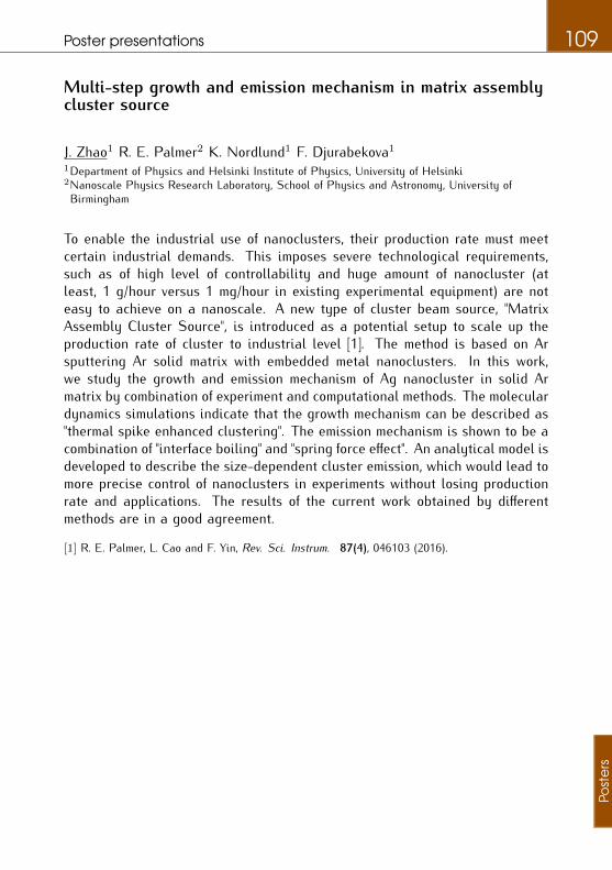
Poster presentations 109
Multi-step growth and emission mechanism in matrix assemblycluster source
J. Zhao1 R. E. Palmer2 K. Nordlund1 F. Djurabekova1
1Department of Physics and Helsinki Institute of Physics, University of Helsinki2Nanoscale Physics Research Laboratory, School of Physics and Astronomy, University ofBirmingham
To enable the industrial use of nanoclusters, their production rate must meetcertain industrial demands. This imposes severe technological requirements,such as of high level of controllability and huge amount of nanocluster (atleast, 1 g/hour versus 1 mg/hour in existing experimental equipment) are noteasy to achieve on a nanoscale. A new type of cluster beam source, "MatrixAssembly Cluster Source", is introduced as a potential setup to scale up theproduction rate of cluster to industrial level [1]. The method is based on Arsputtering Ar solid matrix with embedded metal nanoclusters. In this work,we study the growth and emission mechanism of Ag nanocluster in solid Armatrix by combination of experiment and computational methods. The moleculardynamics simulations indicate that the growth mechanism can be described as"thermal spike enhanced clustering". The emission mechanism is shown to be acombination of "interface boiling" and "spring force effect". An analytical model isdeveloped to describe the size-dependent cluster emission, which would lead tomore precise control of nanoclusters in experiments without losing productionrate and applications. The results of the current work obtained by differentmethods are in a good agreement.
[1] R. E. Palmer, L. Cao and F. Yin, Rev. Sci. Instrum. 87(4), 046103 (2016).
Post
ers
110 Poster presentations
Colossal Enhancement in Magnetic Moment of FerrimagneticNiCo2O4 via Strain-Doping
S. Zhou1
1Helmholtz-Zentrum-Dresden-Rossendorf
Strain doping has emerged as a powerful technique for efficient control of singleaxis lattice expansion to fine tune and modulates the inaccessible complex cor-related phases in the oxide thin films. We report the fine tuning of the magneticmoment and insulator-metal transition in the ferrimagnetic NiCo2O4 inverse-spinel oxide by creating oxygen deficiencies employing high energy He-ionirradiation. Application of the uniaxial tensile strain, less than 1%, can effec-tively tune the oxygen vacancy driving the system in the colossal increase of themagnetic moment by two-factors in magnitude. This magnetic moment showsscaling with the He-ion irradiation fluence. Our results corroborates well withthe X-ray absorption spectroscopic data which shows the peak-height changesand energy shifts of Co-L2,3 and Ni-L2,3 edge driven by the oxygen vacancy.These results demonstrate a new pathway of decoupling the oxygen contentfrom its typical crystal environment via He-ion ir radiation, useful for designingnew functionalities in other spinel oxide thin films.
Post
ers

TRNM IX 111
ParticipantsAbergel David Sweden [email protected] Abdul Wajid Germany [email protected] Ekaterina Finland [email protected] Alexander Belgium [email protected] Jonathan UK [email protected] Blanca Spain [email protected] Carla Belgium [email protected] James United Kingdom [email protected]üchner Christin Germany [email protected]øggild Peter Denmark [email protected] Ivana Croatia [email protected] Karel Czech Republic [email protected] Jean-Christophe Belgium [email protected] Marc Belgium [email protected] Dijken Sebastiaan Finland [email protected] Flyura Finland [email protected] Dogan Turkey [email protected] Chris France [email protected] Stefan Germany [email protected] Jose A. Switzerland [email protected] Adam Finland [email protected] Valentin Israel [email protected] Christoffer John Patrik Finland [email protected] Fredric Finland [email protected] Andris Germany [email protected] Sarah United Kingdom [email protected] Miroslav Switzerland [email protected] Petrudi Seyed Arsalan Finland [email protected] Christofer Switzerland [email protected] Christoph Austria [email protected] Stephan UK [email protected] Eero Finland [email protected] Anne Germany [email protected] Stefan Austria [email protected] Sampo Finland [email protected] Federico France [email protected] Agnieszka Poland [email protected] Pavel Czech Republic [email protected]ónsson Hannes Iceland [email protected]äger Marc Finland [email protected]ónsson Elvar Örn Finland [email protected]
Ge
ne
ral

112 TRNM IX
Kawai Shigeki Japan [email protected] Shawulienu Finland [email protected] Byung-Hyun Sweden [email protected] Hannu-Pekka Finland [email protected] Jani Austria [email protected] Marko Croatia [email protected] Arkady Germany [email protected] Silvan Germany [email protected] Franciszek Poland [email protected] Artem South Korea [email protected] Andreas Finland [email protected] Luc Spain [email protected] Dominik Czech Republic [email protected] Peter Finland [email protected] Eduard Spain [email protected] Cazalilla Alvaro Finland [email protected] Ursula Austria [email protected] Keith United Kingdom [email protected] Ales Slovenia [email protected] Kimmo Austria [email protected] Alexei Ukraine [email protected] Kai Finland [email protected] Luca Italy luca.ottaviano @aquila.infn.itQuintana Mildred Mexico [email protected] Ioannis Greece [email protected] Rosaria Italy [email protected] Jérémy France [email protected] Yossi Israel [email protected] Fabian Switzerland [email protected] Timothy USA [email protected] Nikos Greece [email protected] Isaac Canada [email protected] Dmitry Belgium [email protected] Camilla Finland [email protected] Polona Slovenia [email protected] Philipp Germany [email protected] Muinos Henrique Finland [email protected] David Hungary [email protected] Matthew Sweden [email protected] Lide Finland [email protected] Junle Finland [email protected] Shengqiang Germany [email protected]
Ge
ne
ral

INDEX 113
Index
Abdelghani, 95Abergel, 58Åhlgren, 106Äkäslompolo, 38Arcon, 64Arenal, 53Argentero, 62Arman, 30Atodiresei, 30Aumayr, 47Avramov, 92Awan, 71Aziz, 96
Baccar, 95Baibuz, 50, 72Bakaev, 73Balaz, 57Barmparis, 51Bayer, 83Bean, 74Beyer, 47Biel, 18Bilteryst, 20Bittencourt, 64, 75, 95Bliokh, 77Blomberg, 105Blood, 16Blügel, 30Briddon, 19Briels, 40Broqvist, 90Brunetti, 52
Buh, 64, 98Buijnsters, 53Bukonte, 96Burson, 41Büchner, 41Bøggild, 67
Caciuc, 30Cantalini, 60Capeta, 34Carva, 57Cascione, 52Casiraghi, 38Charlier, 46Chin, 38Clement, 75Cocchi, 23
Dappe, 18Davelou, 51De Matteis, 52Debliquy, 20Delville, 64Djurabekova, 26, 50, 72, 78, 94, 96,
106, 109Donarelli, 60Draxl, 23Dvorak, 89
Eberle, 55Elibol, 83Emamjomeh, 60Erbahar, 19, 42

114 INDEX
Erbe, 71Euwens, 82Ewels, 19, 42, 76
Facsko, 47, 71Flores-Livas, 63Foster, 24, 80Freilikher, 77Freund, 41Fridlund, 78Fu, 23Fukami, 74
Gauquelin, 91George, 71Ghorbani-Asl, 33Ghosh, 25Girbau, 75Goedecker, 63Gomeniuk, 100Gonzalez, 18Grammatikopoulos, 50Granberg, 26Grandthyll, 82Grigorev, 73Gruber, 47Gulans, 23Gölzhäuser, 47
Haigh, 31Haluska, 55, 61Hartmann, 81, 82Hashemi, 79Heller, 47Henning, 49Herbig, 30Hermansson, 40, 90Heyde, 41Hierold, 55, 61Hofer, 62Hofmann, 28Holmstrom, 80
Holtsch, 81, 82Huang, 33Hummel, 83
Ikeda, 74Ikuhara, 74ILinov, 96Inkinen, 38, 84, 108Iori, 85
Jaglicic, 64Jaksic, 106Jamroz, 35Janas, 91Jansson, 50, 72Jany, 91Jelfs, 16Jelinek, 17Jenni, 55Jones, 16Jonsson, 25Jäger, 86Jäntti, 105Jónsson, 87Jónsson, 25, 87
Kabanov, 98Karlusic, 106Kawai, 22Kezilebieke, 89Kim, 90Kioseoglou, 51Knudsen, 30Komsa, 33, 56, 79Kopidakis, 51Kormanyos, 107Kotakoski, 29, 62, 83, 97, 99, 106Kozubek, 106Kralj, 34Krasheninnikov, 33, 56, 79, 106Kretschmer, 56Krok, 91
Ge
ne
ral
INDEX 115
Kuklin, 92Kullgren, 40, 90Kuzubov, 92Kyritsakis, 72, 94
Lahem, 20Lajaunie, 53Lazaro, 75Lebius, 106Legut, 66Leino, 106Leuthner, 62Levo, 26Liljeroth, 14, 24, 89Liu, 61Llobet, 75, 95Lopez-Cazalilla, 96Ludacka, 97Lytvyn, 100
Majewski, 35Majumdar, 38Mangler, 62, 99Maques, 63McKenna, 37, 74Meyer, 62, 83, 99Michely, 30Mihailovic, 98Mirzayev, 99, 106Mitev, 40Mittelberger, 99Monazam, 99Mrzel, 64, 98Mustonen, 99Müller, 82
Nabok, 23Nazarov, 100Nikiel, 91Nikolenko, 100Nordlund, 26, 50, 78, 96, 106, 109Norris, 96
Ochedowski, 106Ohno, 74Ojanen, 89Ortiz, 18Ottaviano, 60
Pale, 105Palmer, 109Paolucci, 60Pardanaud, 53Pennycook, 62, 99Penttila, 105Perkinson, 96Perrozzi, 60Pielic, 34Pitkänen, 105Plodinec, 34Posselt, 73Puska, 38, 79, 87
Qin, 38Quintana, 102
Rakyta, 107Ramos, 75Raskin, 20Ravnik, 98Remediakis, 51Rentenberger, 97Rinaldi, 52Rinke, 89Rio, 19Ritala, 24Roman, 55, 61Rosenwaks, 49Rusavsky, 100
Saito, 74Sanna, 63Sato, 74Schleberger, 106Schonherr, 71Schulz, 24
Ge
ne
ral

116 INDEX
Seitsonen, 24Selin, 105Shalev, 49Shostak, 92Slobodian, 100Sluban, 64Smidstrup, 25Sowwan, 50Srut Rakic, 34Stokbro, 25Strelchuk, 100Struzzi, 95Susi, 62, 97, 99Sutter, 33Sutter, 33Swager, 13Swaminathan, 49Szajna, 91
Taglieri, 60Tagmatarchis, 19, 48Tamblyn, 103Tang, 20Terentyev, 73, 104Thamri, 95Tittonen, 105Toma, 52Tossi, 105Tripathi, 97Tuomisto, 38Turchanin, 47, 71Tyagulskiy, 100
Umek, 64
Valerius, 30van den Bos, 91van Dijken, 38, 84, 108van Tendeloo, 91Vasin, 100Vazquez, 106Vengust, 98
Verbeeck, 91Vernieres, 50Vierimaa, 33Vijayakumar, 38Vilfan, 98Visontai, 107Vujicic, 34
Wegner, 19Wilhammar, 91Wilhelm, 47Will, 30Wolf, 40, 90
Yao, 38, 84, 108
Zhao, 50, 109Zhou, 110Zhurkin, 73Zugarramurdi, 38
Ge
ne
ral

TRNM IX 117
Ge
ne
ral

118 TRNM IX
Ge
ne
ral

TRNM IX 119
Ge
ne
ral

120 TRNM IX
Ge
ne
ral