TMC262 / TMC262C DATASHEET - Trinamic Motion Control
62
POWER DRIVER FOR STEPPER MOTORS INTEGRATED CIRCUITS TRINAMIC Motion Control GmbH & Co. KG Hamburg, Germany TMC262 / TMC262C DATASHEET BLOCK DIAGRAM FEATURES AND BENEFITS High Motor Current up to 10A using external (N&P) MOSFETs. Highest Voltage up to 60V DC operating voltage Highest Resolution up to 256 microsteps per full step Small Size 5x5mm QFN32 package Low Power Dissipation synchronous rectification EMI-optimized slope & current controlled gate drivers Protection & Diagnostics short to GND, overtemperature & undervoltage; short to VS & overcurrent (TMC262C only) StallGuard2™ high precision sensorless motor load detection CoolStep™ load dependent current control saves up to 75% MicroPlyer™ 256 microstep smoothness with 1/16 step input. SpreadCycle™ high-precision chopper for best current sine wave form and zero crossing Improved Silent Motor operation (TMC262C only) Clock Failsafe option for external clock (TMC262C only) APPLICATIONS Textile, Sewing Machines Factory Automation Lab Automation Liquid Handling Medical Office Automation Printer and Scanner CCTV, Security ATM, Cash recycler POS Pumps and Valves Heliostat Controller CNC Machines DESCRIPTION The TMC262/TMC262C drivers for two-phase stepper motors offer an industry-leading feature set, including high-resolution micro-stepping, sensorless mechanical load measurement, load-adaptive power opti- mization, and low-resonance chopper ope- ration. Standard SPI™ and STEP/DIR interfaces simplify communication. The TMC262 uses four external N- and P- channel dual-MOSFETs for motor currents up to 8A RMS and up to 60V. Integrated protection and diagnostic features support robust and reliable operation. High integration, high energy efficiency and small form factor enable miniaturized designs with low external component count for cost-effective and highly competitive solutions. The new –C device improves motor silence and adds low side short protection. Universal, cost-effective stepper driver for two-phase bipolar motors with state-of-the-art features. External MOSFETs fit different motor sizes. With Step/Dir Interface and SPI.
Transcript of TMC262 / TMC262C DATASHEET - Trinamic Motion Control

POWER DRIVER FOR STEPPER MOTORS INTEGRATED CIRCUITS
TRINAMIC Motion Control GmbH & Co. KG Hamburg, Germany
TMC262 / TMC262C DATASHEET
BLOCK DIAGRAM
FEATURES AND BENEFITS
High Motor Current up to 10A using external (N&P) MOSFETs.
Highest Voltage up to 60V DC operating voltage
Highest Resolution up to 256 microsteps per full step
Small Size 5x5mm QFN32 package
Low Power Dissipation synchronous rectification
EMI-optimized slope & current controlled gate drivers
Protection & Diagnostics short to GND, overtemperature & undervoltage; short to VS & overcurrent (TMC262C only)
StallGuard2™ high precision sensorless motor load detection
CoolStep™ load dependent current control saves up to 75%
MicroPlyer™ 256 microstep smoothness with 1/16 step input.
SpreadCycle™ high-precision chopper for best current sine
wave form and zero crossing
Improved Silent Motor operation (TMC262C only)
Clock Failsafe option for external clock (TMC262C only)
APPLICATIONS
Textile, Sewing Machines Factory Automation Lab Automation Liquid Handling Medical Office Automation Printer and Scanner CCTV, Security ATM, Cash recycler POS Pumps and Valves Heliostat Controller CNC Machines
DESCRIPTION
The TMC262/TMC262C drivers for two-phase stepper motors offer an industry-leading feature set, including high-resolution micro-stepping, sensorless mechanical load measurement, load-adaptive power opti-mization, and low-resonance chopper ope-ration. Standard SPI™ and STEP/DIR interfaces simplify communication. The TMC262 uses four external N- and P-channel dual-MOSFETs for motor currents up to 8A RMS and up to 60V. Integrated protection and diagnostic features support robust and reliable operation. High integration, high energy efficiency and small form factor enable miniaturized designs with low external component count for cost-effective and highly competitive solutions. The new –C device improves motor silence and adds low side short protection.
Universal, cost-effective stepper driver for two-phase bipolar motors with state-of-the-art features.
External MOSFETs fit different motor sizes. With Step/Dir Interface and SPI.

TMC262/TMC262C DATASHEET (V2.25 / 2020-JUN-08) 2
www.trinamic.com
Layout for Evaluation
APPLICATION EXAMPLES: HIGH POWER – SMALL SIZE
The TMC262/TMC262C scores with its high power density and a versatility that covers a wide spectrum of applications and motor sizes, all while keeping costs down. Extensive support at the chip, board, and software levels enables rapid design cycles and fast time-to-market with competitive products. High energy efficiency from TRINAMIC’s CoolStep technology delivers further cost savings in related systems such as power supplies and cooling.
Layout with 6A MOSFETs
Miniaturized Layout
ORDER CODES
Device PN Description Size
TMC262C-LA 00-0167 CoolStep™ driver for external MOSFETs, QFN32 5 x 5 mm2
TMC262-LA 00-0075 CoolStep™ driver for external MOSFETs, QFN32 5 x 5 mm2
TMC262x-LA-T …T -T devices are packaged in tape on reel (x=empty or C)
TMC429+26x-EVAL 40-0030 Chipset evaluation board for TMC429, TMC260, TMC261, TMC262, and TMC424.
16 x 10 cm2
LANDUNGSBRÜCKE 40-0167 Baseboard for evaluation boards 85 x 55
ESELSBRÜCKE 40-0098 Connector board for plug-in evaluation board system 61 x 38
*) The Term TMC262 is used for TMC262 or TMC262C within this datasheet. Differences in the TMC262C are explicitly marked with TMC262C. See summary in section 14.
STEPROCKER™
The driver stage shown uses 6A-capable dual MOSFETs. All cooling requirements are satisfied by passive convection cooling. The stepRocker is supported by the motioncontrol-community, with forum, applications, schematics, open source projects, demos etc.:
TMCM-MODULE FOR NEMA 11 STEPPER MOTORS
This miniaturized power stage drives up to 1.2A RMS and mounts directly on a 28mm-size motor. Tiny TSOP6 dual MOSFETs enable an ultra-compact and flexible PCB layout.
TMC262-EVAL DEVELOPMENT PLATFORM
This evaluation board is a development platform for applications based on the TMC262C.
External power MOSFETs support drive currents up to 4A RMS and up to 40V peak supply voltage.
The evaluation board system based on the CPU board LANDUNGSBRÜCKE features an USB interface for communication with the learning and development control software TMCL-IDE running on a PC.
The control software provides a user-friendly GUI for setting control parameters and visualizing the dynamic response of the motor.

TMC262/TMC262C DATASHEET (V2.25 / 2020-JUN-08) 3
www.trinamic.com
TABLE OF CONTENTS
1 PRINCIPLES OF OPERATION ......................... 4
1.1 KEY CONCEPTS ............................................... 4 1.2 CONTROL INTERFACES .................................... 5 1.3 MECHANICAL LOAD SENSING ......................... 5 1.4 CURRENT CONTROL ........................................ 5
2 PIN ASSIGNMENTS ........................................... 6
2.1 PACKAGE OUTLINE ......................................... 6 2.2 SIGNAL DESCRIPTIONS .................................. 6
3 INTERNAL ARCHITECTURE ............................. 8
3.1 STANDARD APPLICATION CIRCUIT .................. 9
4 STALLGUARD2 LOAD MEASUREMENT ....... 10
4.1 TUNING THE STALLGUARD2 THRESHOLD ...... 11 4.2 STALLGUARD2 MEASUREMENT FREQUENCY
AND FILTERING ............................................ 12 4.3 DETECTING A MOTOR STALL ........................ 13 4.4 LIMITS OF STALLGUARD2 OPERATION ......... 13
5 COOLSTEP LOAD-ADAPTIVE CURRENT CONTROL ........................................................... 14
5.1 TUNING COOLSTEP ...................................... 16
6 SPI INTERFACE ................................................ 17
6.1 BUS SIGNALS............................................... 17 6.2 BUS TIMING ................................................ 17 6.3 BUS ARCHITECTURE ..................................... 18 6.4 REGISTER WRITE COMMANDS ...................... 19 6.5 DRIVER CONTROL REGISTER (DRVCTRL) .... 21 6.6 CHOPPER CONTROL REGISTER (CHOPCONF) ..
................................................................... 23 6.7 COOLSTEP CONTROL REGISTER (SMARTEN) ...
................................................................... 24 6.8 STALLGUARD2 CONTROL REGISTER
(SGCSCONF) ............................................. 25 6.9 DRIVER CONTROL REGISTER (DRVCONF) ... 26 6.10 READ RESPONSE .......................................... 27 6.11 DEVICE INITIALIZATION ............................... 28
7 STEP/DIR INTERFACE ..................................... 29
7.1 TIMING ........................................................ 29 7.2 MICROSTEP TABLE ....................................... 30 7.3 CHANGING RESOLUTION .............................. 31 7.4 MICROPLYER STEP INTERPOLATOR ............... 31 7.5 STANDSTILL CURRENT REDUCTION ............... 32
8 CURRENT SETTING .......................................... 33
8.1 SENSE RESISTORS ........................................ 34
9 CHOPPER OPERATION ................................... 35
9.1 SPREADCYCLE CHOPPER ............................... 36 9.2 CLASSIC CONSTANT OFF-TIME CHOPPER ..... 39
10 POWER MOSFET STAGE ................................ 41
10.1 BREAK-BEFORE-MAKE LOGIC ........................ 41
10.2 ENN INPUT ................................................. 41 10.3 SLOPE CONTROL .......................................... 41
11 DIAGNOSTICS AND PROTECTION ............. 43
11.1 SHORT PROTECTION..................................... 43 11.2 OPEN-LOAD DETECTION .............................. 44 11.3 TEMPERATURE SENSORS ............................... 45 11.4 UNDERVOLTAGE DETECTION ......................... 45
12 POWER SUPPLY SEQUENCING .................... 46
13 SYSTEM CLOCK ................................................ 47
13.1 FREQUENCY SELECTION ................................ 48
14 TMC262C COMPATIBILITY ........................... 49
15 MOSFET EXAMPLES ......................................... 50
16 LAYOUT CONSIDERATIONS ......................... 51
16.1 SENSE RESISTORS ........................................ 51 16.2 EXPOSED DIE PAD ....................................... 51 16.3 POWER FILTERING ....................................... 51 16.4 THERMAL RESISTANCE ................................. 51 16.5 LAYOUT EXAMPLE ........................................ 52
17 ABSOLUTE MAXIMUM RATINGS ................. 54
18 ELECTRICAL CHARACTERISTICS ................. 55
18.1 OPERATIONAL RANGE .................................. 55 18.2 DC AND AC SPECIFICATIONS ...................... 55
19 PACKAGE MECHANICAL DATA .................... 59
19.1 DIMENSIONAL DRAWINGS ........................... 59 19.2 PACKAGE CODE ........................................... 60
20 DISCLAIMER ..................................................... 60
21 ESD SENSITIVE DEVICE ................................ 60
22 TABLE OF FIGURES ......................................... 61
23 REVISION HISTORY ....................................... 62
24 REFERENCES ...................................................... 62

TMC262 / TMC262C DATASHEET (Rev. 2.25 / 2020-JUN-08) 4
www.trinamic.com
1 Principles of Operation
µC
SPI
TMC262MOSFET
Driver Stage
NSS/D
0A+
0A-
0B+
0B-
High-Level Interface
µC
SPI
SPITMC262
MOSFETDriver Stage
NSS/D
0A+
0A-
0B+
0B-
TMC429Motion
Controllerfor up to
3 Motors
High-Level Interface
Figure 1.1 Applications block diagrams
The TMC262 motor driver is the intelligence between a motion controller and the power MOSFETs for driving a two-phase stepper motor, as shown in Figure 1.1 Following power-up, an embedded microcontroller initializes the driver by sending commands over an SPI bus to write control parameters and mode bits in the TMC262. The microcontroller may implement the motion-control function as shown in the upper part of the figure, or it may send commands to a dedicated motion controller chip such as TRINAMIC’s TMC429 as shown in the lower part. The motion controller can control the motor position by sending pulses on the STEP signal while indicating the direction on the DIR signal. The TMC262 has a microstep counter and sine table to convert these signals into the coil currents which control the position of the motor. If the microcontroller implements the motion-control function, it can write values for the coil currents directly to the TMC262 over the SPI interface, in which case the STEP/DIR interface may be disabled. This mode of operation requires software to track the motor position and reference a sine table to calculate the coil currents. To optimize power consumption and heat dissipation, software may also adjust CoolStep and StallGuard2 parameters in real-time, for example to implement different tradeoffs between speed and power consumption in different modes of operation. The motion control function is a hard real-time task which may be a burden to implement reliably alongside other tasks on the embedded microcontroller. By offloading the motion-control function to the TMC429, up to three motors can be operated reliably with very little demand for service from the microcontroller. Software only needs to send target positions, and the TMC429 generates precisely timed step pulses. Software retains full control over both the TMC262 and TMC429 through the SPI bus.
1.1 Key Concepts The TMC262 motor driver implements several advanced patented features which are exclusive to TRINAMIC products. These features contribute toward greater precision, greater energy efficiency, higher reliability, smoother motion, and cooler operation in many stepper motor applications.
StallGuard2™ High-precision load measurement using the back EMF on the coils
CoolStep™ Load-adaptive current control which reduces energy consumption by as much as
75%
SpreadCycle™ High-precision chopper algorithm available as an alternative to the traditional
constant off-time algorithm
MicroPlyer™ Microstep interpolator for obtaining increased smoothness of microstepping over a STEP/DIR interface

TMC262 / TMC262C DATASHEET (Rev. 2.25 / 2020-JUN-08) 5
www.trinamic.com
In addition to these performance enhancements, TRINAMIC motor drivers also offer safeguards to detect and protect against shorted outputs, open-circuit output, overtemperature, and undervoltage conditions for enhancing safety and recovery from equipment malfunctions.
1.2 Control Interfaces There are two control interfaces from the motion controller to the motor driver: the SPI serial interface and the STEP/DIR interface. The SPI interface is used to write control information to the chip and read back status information. This interface must be used to initialize parameters and modes necessary to enable driving the motor. This interface may also be used for directly setting the currents flowing through the motor coils, as an alternative to stepping the motor using the STEP and DIR signals, so the motor can be controlled through the SPI interface alone. The STEP/DIR interface is a traditional motor control interface available for adapting existing designs to use TRINAMIC motor drivers. Using only the SPI interface requires slightly more CPU overhead to look up the sine tables and send out new current values for the coils.
1.2.1 SPI Interface The SPI interface is a bit-serial interface synchronous to a bus clock. For every bit sent from the bus master to the bus slave, another bit is sent simultaneously from the slave to the master. Communication between an SPI master and the TMC262 slave always consists of sending one 20-bit command word and receiving one 20-bit status word. For purely SPI-controlled operation, the SPI command rate typically corresponds to the microstep rate at low velocities. At high velocities, the rate may be limited by CPU bandwidth to 10-100 thousand commands per second, so the application may need to change to fullstep resolution.
1.2.2 STEP/DIR Interface The STEP/DIR interface is enabled by default. Active edges on the STEP input can be rising edges or both rising and falling edges, as controlled by another mode bit (DEDGE). Using both edges cuts the toggle rate of the STEP signal in half, which is useful for communication over slow interfaces such as optically isolated interfaces. On each active edge, the state sampled from the DIR input determines whether to step forward or back. Each step can be a fullstep or a microstep, in which there are 2, 4, 8, 16, 32, 64, 128, or 256 microsteps per fullstep. During microstepping, a low state on DIR increases the microstep counter and a high decreases the counter by an amount controlled by the microstep resolution. An internal table translates the counter value into the sine and cosine values which control the motor current for microstepping.
1.3 Mechanical Load Sensing The TMC262 provides StallGuard2 high-resolution load measurement for determining the mechanical load on the motor by measuring the back EMF. In addition to detecting when a motor stalls, this feature can be used for homing to a mechanical stop without a limit switch or proximity detector. The CoolStep power-saving mechanism uses StallGuard2 to reduce the motor current to the minimum motor current required to meet the actual load placed on the motor.
1.4 Current Control Current into the motor coils is controlled using a cycle-by-cycle chopper mode. Two chopper modes are available: a traditional constant off-time mode and the new SpreadCycle mode. SpreadCycle mode offers smoother operation and greater power efficiency over a wide range of speed and load.

TMC262 / TMC262C DATASHEET (Rev. 2.25 / 2020-JUN-08) 6
www.trinamic.com
2 Pin Assignments
2.1 Package Outline
GND
HA1
HA2
BMA2
BMA1
SRA
VCC_I
O
VS
CSN
GND
SDI
SCK
SRB
LB2
LB1
BMB1
BMB2
HB2
HB1
VHS
CLK
Top view
LA1
LA2
32 31 30 29 28 27 26 25
9 10 11 12 13 14 15 16
1718
1920
2122
2324
12
34
56
78
TMC 262-LA
ENN
SDO
5VOUT
TST_
ANA
SG_T
ST
GNDP
DIR
STE
P
TST_
MODE
Figure 2.1 TMC262 pin assignments
2.2 Signal Descriptions Pin Number Type Function
GND, GNDP, exposed pad
1 GND pads for different parts of the internal circuitry. Tie all GND pins and the die attach pad to a solid common GND plane. Directly connect the sense resistor GND side to this GND plane.
13
28
HA1 2 O (VS) High side P-channel driver output. Becomes driven to VHS to switch on MOSFET. HA2 3
HB1 23
HB2 22
BMA1 5 I (VS) Sensing input for bridge outputs. Used for short to GND protection. May be tied to VS if unused. BMA2 4
BMB1 20
BMB2 21
LA1 6 O 5V Low side MOSFET driver output. Becomes driven to 5VOUT to switch on MOSFET. LA2 7
LB1 19
LB2 18
SRA 8 AI Sense resistor input of chopper driver.
SRB 17

TMC262 / TMC262C DATASHEET (Rev. 2.25 / 2020-JUN-08) 7
www.trinamic.com
Pin Number Type Function
5VOUT 9 Output of internal 5V linear regulator. This voltage is used to supply the low-side drivers and internal analog circuitry. An external capacitor to GND close to the pin is required. Place the capacitor near to pin 9 and connect the other side to the GND plane. 470nF ceramic is sufficient for most applications; an additional low-ESR capacitor (10µF or more) improves performance with high gate charge MOSFETs.
SDO 10 DO VIO Data output of SPI interface (Tristate)
SDI 11 DI VIO Data input of SPI interface (Scan test input in test mode)
SCK 12 DI VIO Serial clock input of SPI interface (Scan test shift enable input in test mode)
CSN 14 DI VIO Chip select input of SPI interface
ENN 15 DI VIO Enable not input for drivers. Switches off all MOSFETs.
CLK 16 DI VIO Clock input for all internal operations. Tie low to use internal oscillator. The first high signal disables the internal oscillator until power down.
VHS 24 High side supply voltage (motor supply voltage VS - 10V)
VS 25 Motor supply voltage
TST_ANA 26 AO VIO Analog mode test output. Leave open for normal operation.
SG_TST 27 DO VIO StallGuard2™ output. Signals motor stall (high active).
VCC_IO 29 Input / output supply voltage VIO for all digital pins. Tie to digital logic supply voltage. Allows operation in 3.3V and 5V systems.
DIR 30 DI VIO Direction input. Is sampled upon detection of a step to determine stepping direction. An internal glitch filter for 60ns is provided.
STEP 31 DI VIO Step input. An internal glitch filter for 60ns is provided.
TST_MODE 32 DI VIO Test mode input. Puts IC into test mode. Tie to GND for normal operation using a short wire to GND plane.
TMC262 / TMC262C DATASHEET (Rev. 2.25 / 2020-JUN-08) 8
www.trinamic.com
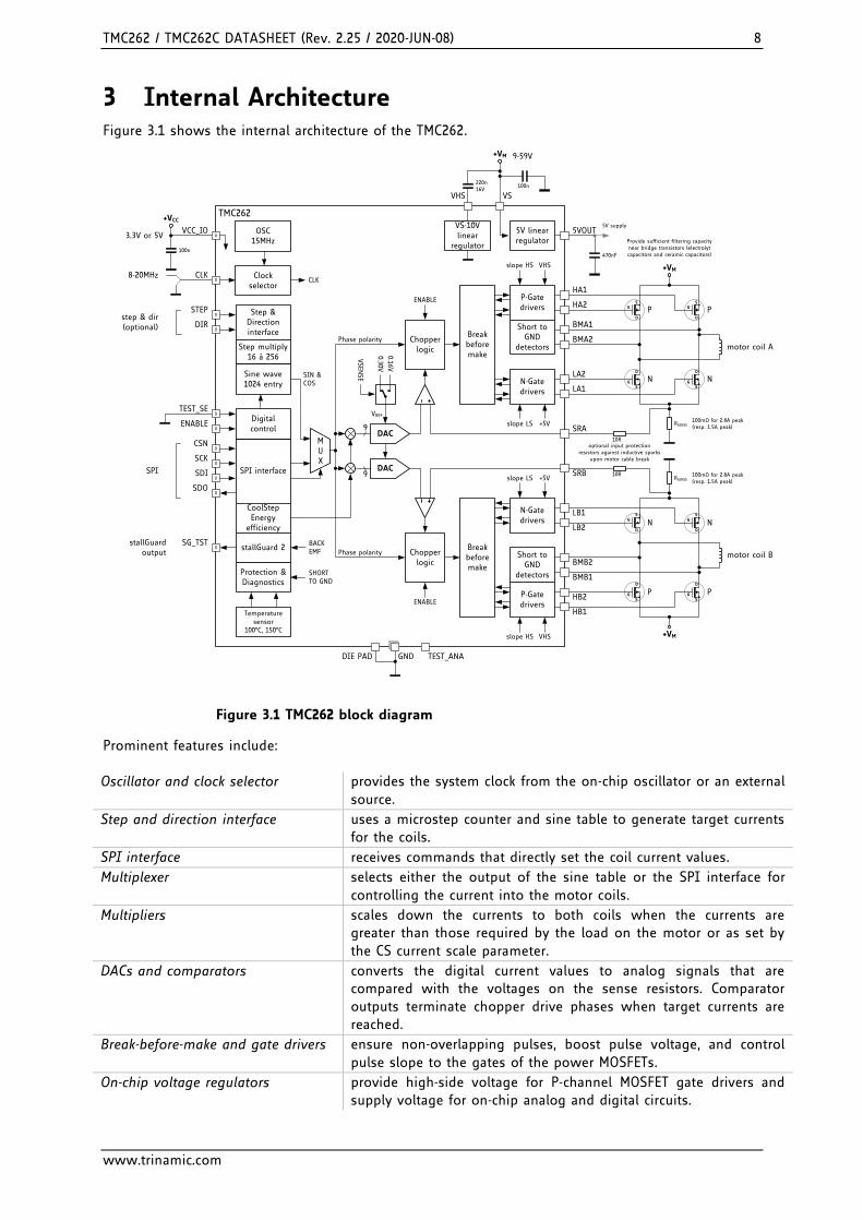
3 Internal Architecture Figure 3.1 shows the internal architecture of the TMC262.
+VM
+VM
VHS
5V linear regulator
5VOUT
470nF
VS
GND
slope HS
slope LSSRAD
ENABLE
5V supply
TMC262
OSC15MHz
CSND
SCK
SDI
D
D
SDOD
RSENSE
DIE PAD
SPI interface
Chopper logic
100mΩ for 2.8A peak (resp. 1.5A peak)
Provide sufficient filtering capacity near bridge transistors (electrolyt capacitors and ceramic capacitors)
S
D
G
S
D
G
P
N
motor coil A
HA2
HA1
BMA1
BMA2
S
D
G
S
D
G
P
NLA1
LA2
P-Gate drivers
Short to GND
detectors
N-Gate drivers
Break before make
VHS
+5V9
DAC
VS-10Vlinear
regulator
220n16V
100n
Protection & Diagnostics
+VMslope HS
slope LSSRB
RSENSE
Chopper logic
100mΩ for 2.8A peak (resp. 1.5A peak)
S
D
G
S
D
G
P
N
motor coil B
HB2
HB1
BMB1
BMB2
S
D
G
S
D
G
P
NLB1
LB2
P-Gate drivers
Short to GND
detectors
N-Gate drivers
Break before make
VHS
+5V9
DAC
ENABLE
ENABLE
Step & Direction interface
Step multiply16 à 256
Sine wave 1024 entry
MUX
STEPD
DIRD
Temperature sensor
100°C, 150°C
CoolStepEnergy
efficiency
stallGuard 2
Clock selector
CLKD
SG_TST
Digital control
D
SHORT TO GND
BACK EMF
CLK8-20MHz
SIN & COS
Phase polarity
Phase polarity
VCC_IOD
DTEST_SE
3.3V or 5V
+VCC
100n
9-59V
step & dir (optional)
SPI
stallGuard output
TEST_ANA
10R
10R
optional input protection resistors against inductive sparks
upon motor cable break
VSEN
SE
0.30V
0.16V
VREF
Figure 3.1 TMC262 block diagram
Prominent features include: Oscillator and clock selector provides the system clock from the on-chip oscillator or an external
source.
Step and direction interface uses a microstep counter and sine table to generate target currents for the coils.
SPI interface receives commands that directly set the coil current values.
Multiplexer selects either the output of the sine table or the SPI interface for
controlling the current into the motor coils.
Multipliers scales down the currents to both coils when the currents are greater than those required by the load on the motor or as set by
the CS current scale parameter.
DACs and comparators converts the digital current values to analog signals that are compared with the voltages on the sense resistors. Comparator outputs terminate chopper drive phases when target currents are reached.
Break-before-make and gate drivers ensure non-overlapping pulses, boost pulse voltage, and control
pulse slope to the gates of the power MOSFETs.
On-chip voltage regulators provide high-side voltage for P-channel MOSFET gate drivers and supply voltage for on-chip analog and digital circuits.

TMC262 / TMC262C DATASHEET (Rev. 2.25 / 2020-JUN-08) 9
www.trinamic.com
3.1 Standard Application circuit
47R
LS
VCC_IO
TMC262
SPI interface
CSN
SCK
SDO
SDI
Step&Dir input with microPlyer
STEP
DIR
stallGuard2
5V Voltage regulator
CLK
SG_TST
+VM
5VOUT
VS
2.2µ
+VIO
DRV_E
NN
GND
TST_
MODE
DIE
PAD
opt. ext. clock12-16MHz
3.3V or 5VI/O voltage
100n
100n
Sequencer
LS
steppermotor
NS
BMA2
Chopper
SRAH
CE
Must be identical
to bridge supply!
Use low inductivity SMD
type, e.g. 1210 or 2512
resistor for RS!
TST_
ANA
opt. driver enable
B.Dwersteg, ©
TRINAMIC 2014
RS
LA1
LA2
HA1
HA2
BMA1HS
HS
+VM
LS
LS
BMB2
SRBH
RS
LB1
LB2
HB1
HB2
BMB1HS
HS
+VM
VS-10V regulator
VHS
220n
TEST OUT
470n
470n
Keep inductivity of the fat
interconnections as small as
possible to avoid ringing!
47R
pdVS
VHS
5V
VS
VHS
5V
pd
Leave unconnected
C5VOUT: 470nF to 10µF
(higher for lower noise chopper)
CVHS: 220nF to 1µF
(both higher for higher MOSFET gate
charge)
SPI interface for
configuration or for driving
(optional to Step/Dir)
Configuration pins in stand
alone mode
Stall detection pulse
(react to first impulse /
ignore outside velocity
window)
Tie to the same GND plane
as the sense resistor s GND
Figure 2 Standard application circuit
The standard application uses a minimum number of external components in order to operate the stepper motor. Four N-channel and four P-channel MOSFETs are required, and shall be selected as required for the application motor current. See chapter 15 for examples. With N&P channel FETs, no charge-pump is required, making the design small and robust. Two sense resistors set the motor coil current. See chapter 8 for the calculation of the right sense resistor value. Use low ESR capacitors for filtering the power supply. A minimum of 100µF per ampere of coil current near to the power bridge is recommended for best performance. These capacitors need to cope with the current ripple caused by chopper operation, thus they should not be dimensioned too small. Current ripple in the supply capacitors also depends on the power supply internal resistance and cable length. VCC_IO can be supplied from 5VOUT, or from an external source, e.g. 3.3V.
Basic layout hints Place sense resistors and all filter capacitors as close as possible to the power MOSFETs. Place the TMC262 near to the MOSFETs and use short interconnection lines in order to minimize parasitic trace inductance. Use a solid common GND for GND and die pad GND connections, also for sense resistor GND. Connect 5VOUT filtering capacitor directly to 5VOUT and GND plane. See layout hints for more details. High capacity ceramic or low ESR electrolytic capacitors are recommended for VS filtering.

TMC262 / TMC262C DATASHEET (Rev. 2.25 / 2020-JUN-08) 10
www.trinamic.com
4 StallGuard2 Load Measurement StallGuard2 provides an accurate measurement of the load on the motor. It can be used for stall detection as well as other uses at loads below those which stall the motor, such as CoolStep load-adaptive current reduction. (StallGuard2 is a more precise evolution of the earlier StallGuard technology.) The StallGuard2 measurement value changes linearly over a wide range of load, velocity, and current settings, as shown in Figure 4.1. At maximum motor load, the value goes to zero or near to zero. This corresponds to a load angle of 90° between the magnetic field of the coils and magnets in the rotor. This also is the most energy-efficient point of operation for the motor.
motor load (% max. torque)
stallGuard2 reading
100
200
300
400
500
600
700
800
900
1000
0 10 20 30 40 50 60 70 80 90 100
Start value depends on motor and operating conditions
Motor stalls above this point. Load angle exceeds 90° and available torque sinks.
stallGuard value reaches zero and indicates danger of stall.
This point is set by stallGuard threshold value SGT.
Figure 4.1 StallGuard2 load measurement SG as a function of load
Two parameters control StallGuard2 and one status value is returned.
Parameter Description Setting Comment
SGT 7-bit signed integer that sets the StallGuard2 threshold level for asserting the SG_TST output and sets the optimum measurement range for readout. Negative values increase sensitivity, and positive values reduce sensitivity so more torque is required to indicate a stall. Zero is a good starting value. Operating at values below -10 is not recommended.
0 indifferent value
+1… +63 less sensitivity
-1… -64 higher sensitivity
SFILT Mode bit which enables the StallGuard2 filter for more precision. If set, reduces the measurement frequency to one measurement per four fullsteps. If cleared, no filtering is performed. Filtering compensates for mechanical asymmetries in the construction of the motor, but at the expense of response time. Unfiltered operation is recommended for rapid stall detection. Filtered operation is recommended for more precise load measurement.
0 standard mode
1 filtered mode
TMC262 / TMC262C DATASHEET (Rev. 2.25 / 2020-JUN-08) 11
www.trinamic.com
Status word Description Range Comment
SG 10-bit unsigned integer StallGuard2 measure-ment value. A higher value indicates lower mechanical load. A lower value indicates a higher load and therefore a higher load angle. For stall detection, adjust SGT to return an SG value of 0 or slightly higher upon maximum motor load before stall.
0… 1023 0: highest load low value: high load high value: less load
4.1 Tuning the StallGuard2 Threshold Due to the dependency of the StallGuard2 value SG from motor-specific characteristics and application-specific demands on load and velocity the easiest way to tune the StallGuard2 threshold SGT for a specific motor type and operating conditions is interactive tuning in the actual application. The procedure is:
1. Operate the motor at a reasonable velocity for your application and monitor SG. 2. Apply slowly increasing mechanical load to the motor. If the motor stalls before SG reaches
zero, decrease SGT. If SG reaches zero before the motor stalls, increase SGT. A good SGT starting value is zero. SGT is signed, so it can have negative or positive values.
3. The optimum setting is reached when SG is between 0 and 400 at increasing load shortly before the motor stalls, and SG increases by 100 or more without load. SGT in most cases can be tuned together with the motion velocity in a way that SG goes to zero when the motor stalls and the stall output SG_TST is asserted. This indicates that a step has been lost.
The system clock frequency affects SG. An external crystal-stabilized clock should be used for applications that demand the highest performance. The power supply voltage also affects SG, so tighter regulation results in more accurate values. SG measurement has a high resolution, and there are a few ways to enhance its accuracy, as described in the following sections.
4.1.1 Variable Velocity Operation Across a range of velocities, on-the-fly adjustment of the StallGuard2 threshold SGT improves the accuracy of the load measurement SG. This also improves the power reduction provided by CoolStep, which is driven by SG. Linear interpolation between two SGT values optimized at different velocities is a simple algorithm for obtaining most of the benefits of on-the-fly SGT adjustment, as shown in Figure 4.2. This figure shows an optimal SGT curve in black and a two-point interpolated SGT curve in red.

TMC262 / TMC262C DATASHEET (Rev. 2.25 / 2020-JUN-08) 12
www.trinamic.com
back EMF reaches supply voltage
optimum SGT setting
Motor RPM(200 FS motor)
stallGuard2 reading at
no load
2
4
6
8
10
12
14
16
100
200
300
400
500
600
700
800
900
1000
18
20
0 0 50 100 150 200 250 300 350 400 450 500 550 600
lower limit for stall detection 4 RPM
simplified SGT setting
Figure 4.2 Linear interpolation for optimizing SGT with changes in velocity
4.1.2 Small Motors with High Torque Ripple and Resonance Motors with a high detent torque show an increased variation of the StallGuard2 measurement value SG with varying motor currents, especially at low currents. For these motors, the current dependency might need correction in a similar manner to velocity correction for obtaining the highest accuracy.
4.1.3 Temperature Dependence of Motor Coil Resistance Motors working over a wide temperature range may require temperature correction, because motor coil resistance increases with rising temperature. This can be corrected as a linear reduction of SG at increasing temperature, as motor efficiency is reduced.
4.1.4 Accuracy and Reproducibility of StallGuard2 Measurement In a production environment, it may be desirable to use a fixed SGT value within an application for one motor type. Most of the unit-to-unit variation in StallGuard2 measurements results from manufacturing tolerances in motor construction. The measurement error of StallGuard2 – provided that all other parameters remain stable – can be as low as: 𝑠𝑡𝑎𝑙𝑙𝐺𝑢𝑎𝑟𝑑 𝑚𝑒𝑎𝑠𝑢𝑟𝑒𝑚𝑒𝑛𝑡 𝑒𝑟𝑟𝑜𝑟 = ±𝑚𝑎𝑥(1, |𝑆𝐺𝑇|)
4.2 StallGuard2 Measurement Frequency and Filtering The StallGuard2 measurement value SG is updated with each full step of the motor. This is enough to safely detect a stall, because a stall always means the loss of four full steps. In a practical application, especially when using CoolStep, a more precise measurement might be more important than an update for each fullstep because the mechanical load never changes instantaneously from one step to the next. For these applications, the SFILT bit enables a filtering function over four load measurements. The filter should always be enabled when high-precision measurement is required. It compensates for variations in motor construction, for example due to misalignment of the phase A to phase B magnets. The filter should only be disabled when rapid response to increasing load is required, such as for stall detection at high velocity.

TMC262 / TMC262C DATASHEET (Rev. 2.25 / 2020-JUN-08) 13
www.trinamic.com
4.3 Detecting a Motor Stall To safely detect a motor stall, a stall threshold must be determined using a specific SGT setting. Therefore, you need to determine the maximum load the motor can drive without stalling and to monitor the SG value at this load, for example some value within the range 0 to 400. The stall threshold should be a value safely within the operating limits, to allow for parameter stray. So, your microcontroller software should set a stall threshold which is slightly higher than the minimum value seen before an actual motor stall occurs. The response at an SGT setting at or near 0 gives some idea on the quality of the signal: Check the SG value without load and with maximum load. These values should show a difference of at least 100 or a few 100, which shall be large compared to the offset. If you set the SGT value so that a reading of 0 occurs at maximum motor load, an active high stall output signal will be available at SG_TST output.
4.4 Limits of StallGuard2 Operation StallGuard2 does not operate reliably at extreme motor velocities: Very low motor velocities (for many motors, less than one revolution per second) generate a low back EMF and make the measurement unstable and dependent on environment conditions (temperature, etc.). Other conditions will also lead to extreme settings of SGT and poor response of the measurement value SG to the motor load. Very high motor velocities, in which the full sinusoidal current is not driven into the motor coils also lead to poor response. These velocities are typically characterized by the motor back EMF reaching the supply voltage.

TMC262 / TMC262C DATASHEET (Rev. 2.25 / 2020-JUN-08) 14
www.trinamic.com
5 CoolStep Load-Adaptive Current Control CoolStep allows substantial energy savings, especially for motors which see varying loads or operate at a high duty cycle. Because a stepper motor application needs to work with a torque reserve of 30% to 50%, even a constant-load application allows significant energy savings because CoolStep automatically enables torque reserve when required. Reducing power consumption keeps the system cooler, increases motor life, and allows reducing cost in the power supply and cooling components.
Hint Reducing motor current by half results in reducing power by a factor of four.
Energy efficiency - power consumption decreased up to 75%. Motor generates less heat - improved mechanical precision. Less cooling infrastructure - for motor and driver. Cheaper motor - does the job.
0
0,1
0,2
0,3
0,4
0,5
0,6
0,7
0,8
0,9
0 50 100 150 200 250 300 350
Efficiency
Velocity [RPM]
Efficiency with coolStep
Efficiency with 50% torque reserve
Figure 5.1 Energy efficiency example with CoolStep
Figure 5.1 shows the efficiency gain of a 42mm stepper motor when using CoolStep compared to standard operation with 50% of torque reserve. CoolStep is enabled above 60rpm in the example. CoolStep is controlled by several parameters, but two are critical for understanding how it works:
Parameter Description Range Comment
SEMIN 4-bit unsigned integer that sets a lower threshold. If SG goes below this threshold, CoolStep increases the current to both coils. The 4-bit SEMIN value is scaled by 32 to cover the lower half of the range of the 10-bit SG value. (The name of this parameter is derived from smartEnergy, which is an earlier name for CoolStep.)
0… 15 lower StallGuard threshold: SEMINx32
SEMAX 4-bit unsigned integer that controls an upper threshold. If SG is sampled equal to or above this threshold enough times, CoolStep decreases the current to both coils. The upper threshold is (SEMIN + SEMAX + 1) x 32.
0… 15 upper StallGuard threshold: (SEMIN+SEMAX+1)x32

TMC262 / TMC262C DATASHEET (Rev. 2.25 / 2020-JUN-08) 15
www.trinamic.com
Figure 5.2 shows the operating regions of CoolStep. The black line represents the SG measurement value, the blue line represents the mechanical load applied to the motor, and the red line represents the current into the motor coils. When the load increases, SG falls below SEMIN, and CoolStep increases the current. When the load decreases and SG rises above (SEMIN + SEMAX + 1) x 32 the current becomes reduced.
stal
lGuar
d2
read
ing
0=maximum load
motor current increment area
motor current reduction area
stall possible
SEMIN
SEMAX+SEMIN+1
time
moto
r cu
rrent
current setting CS (upper limit)
½ or ¼ CS (lower limit)
mech
anical
load
current in
crem
ent due to
incr
eas
ed load
slow
current re
duct
ion d
ue
to reduce
d m
oto
r lo
ad
load angle optimized load angle optimizedload angle
optimized
Figure 5.2 CoolStep adapts motor current to the load
Four more parameters control CoolStep and one status value is returned:
Parameter Description Range Comment
CS Current scale. Scales both coil current values as taken from the internal sine wave table or from the SPI interface. For high precision motor operation, work with a current scaling factor in the range 16 to 31, because scaling down the current values reduces the effective microstep resolution by making microsteps coarser. This setting also controls the maximum current value set by CoolStep™.
0… 31 scaling factor:
1/32, 2/32, … 32/32
SEUP Number of increments of the coil current for each occurrence of an SG measurement below the lower threshold.
0… 3 step width is: 1, 2, 4, 8
SEDN Number of occurrences of SG measurements above the upper threshold before the coil current is decremented.
0… 3 number of StallGuard measurements per decrement: 32, 8, 2, 1
SEIMIN Mode bit that controls the lower limit for scaling the coil current. If the bit is set, the limit is ¼ CS. If the bit is clear, the limit is ½ CS.
0
Minimum motor current: 1/2 of CS
1 1/4 of CS
Status word Description Range Comment
SE 5-bit unsigned integer reporting the actual cur-rent scaling value determined by CoolStep. This value is biased by 1 and divided by 32, so the range is 1/32 to 32/32. The value will not be greater than the value of CS or lower than either ¼ CS or ½ CS depending on SEIMIN setting.
0… 31 Actual motor current scaling factor set by CoolStep: 1/32, 2/32, … 32/32
TMC262 / TMC262C DATASHEET (Rev. 2.25 / 2020-JUN-08) 16
www.trinamic.com
5.1 Tuning CoolStep Before tuning CoolStep, first tune the StallGuard2 threshold level SGT, which affects the range of the load measurement value SG. CoolStep uses SG to operate the motor near the optimum load angle of +90°. The current increment speed is specified in SEUP, and the current decrement speed is specified in SEDN. They can be tuned separately because they are triggered by different events that may need different responses. The encodings for these parameters allow the coil currents to be increased much more quickly than decreased, because crossing the lower threshold is a more serious event that may require a faster response. If the response is too slow, the motor may stall. In contrast, a slow response to crossing the upper threshold does not risk anything more serious than missing an opportunity to save power.
Hint CoolStep operates between limits controlled by the current scale parameter CS and the SEIMIN bit.
5.1.1 Response Time For fast response to increasing motor load, use a high current increment step SEUP. If the motor load changes slowly, a lower current increment step can be used to avoid motor current oscillations. If the filter controlled by SFILT is enabled, the measurement rate and regulation speed are cut by a factor of four.
5.1.2 Low Velocity and Standby Operation Because StallGuard2 is not able to measure the motor load in standstill and at very low RPM, the current at low velocities should be set to an application-specific default value and combined with standstill current reduction settings programmed through the SPI interface.

TMC262 / TMC262C DATASHEET (Rev. 2.25 / 2020-JUN-08) 17
www.trinamic.com
6 SPI Interface The TMC262 allows full control over all configuration parameters and mode bits through the SPI interface. An initialization is required prior to motor operation. The SPI interface also allows reading back status values and bits.
6.1 Bus Signals The SPI bus on the TMC262 has four signals:
SCK bus clock input SDI serial data input SDO serial data output CSN chip select input (active low)
The slave is enabled for an SPI transaction by a low on the chip select input CSN. Bit transfer is synchronous to the bus clock SCK, with the slave latching the data from SDI on the rising edge of SCK and driving data to SDO following the falling edge. The most significant bit is sent first. A minimum of 20 SCK clock cycles is required for a bus transaction with the TMC262. If more than 20 clocks are driven, the additional bits shifted into SDI are shifted out on SDO after a 20-clock delay through an internal shift register. This can be used for daisy chaining multiple chips. CSN must be low during the whole bus transaction. When CSN goes high, the contents of the internal shift register are latched into the internal control register and recognized as a command from the master to the slave. If more than 20 bits are sent, only the last 20 bits received before the rising edge of CSN are recognized as the command.
6.2 Bus Timing SPI interface is synchronized to the internal system clock, which limits the SPI bus clock SCK to half of the system clock frequency. If the system clock is based on the on-chip oscillator, an additional 10% safety margin must be used to ensure reliable data transmission. All SPI inputs as well as the ENN input are internally filtered to avoid triggering on pulses shorter than 20ns. Figure 6.1 shows the timing parameters of an SPI bus transaction, and the table below specifies their values.
CSN
SCK
SDI
SDO
tCC tCCtCL tCH
bit19 bit18 bit0
bit19 bit18 bit0
tDO tZC
tDU tDH
tCH
Figure 6.1 SPI Timing
Hint Usually this SPI timing is referred to as SPI MODE 3
TMC262 / TMC262C DATASHEET (Rev. 2.25 / 2020-JUN-08) 18
www.trinamic.com
SPI Interface Timing AC-Characteristics
clock period is tCLK
Parameter Symbol Conditions Min Typ Max Unit
SCK valid before or after change of CSN
tCC
10 ns
CSN high time
tCSH
*)Min time is for
synchronous CLK with SCK high one tCH before CSN high only
tCLK >2tCLK
+10 ns
SCK low time tCL
*)Min time is for
synchronous CLK only
tCLK >tCLK+10 ns
SCK high time tCH
*)Min time is for
synchronous CLK only
tCLK >tCLK+10 ns
SCK frequency using internal clock
fSCK Assumes minimum OSC frequency 4 MHz
SCK frequency using external 16MHz clock
fSCK Assumes synchronous CLK 8 MHz
SDI setup time before rising edge of SCK
tDU
10 ns
SDI hold time after rising edge of SCK
tDH
10 ns
Data out valid time after falling SCK clock edge
tDO No capacitive load on SDO tFILT+5 ns
SDI, SCK, and CSN filter delay time
tFILT Rising and falling edge 12 20 30 ns
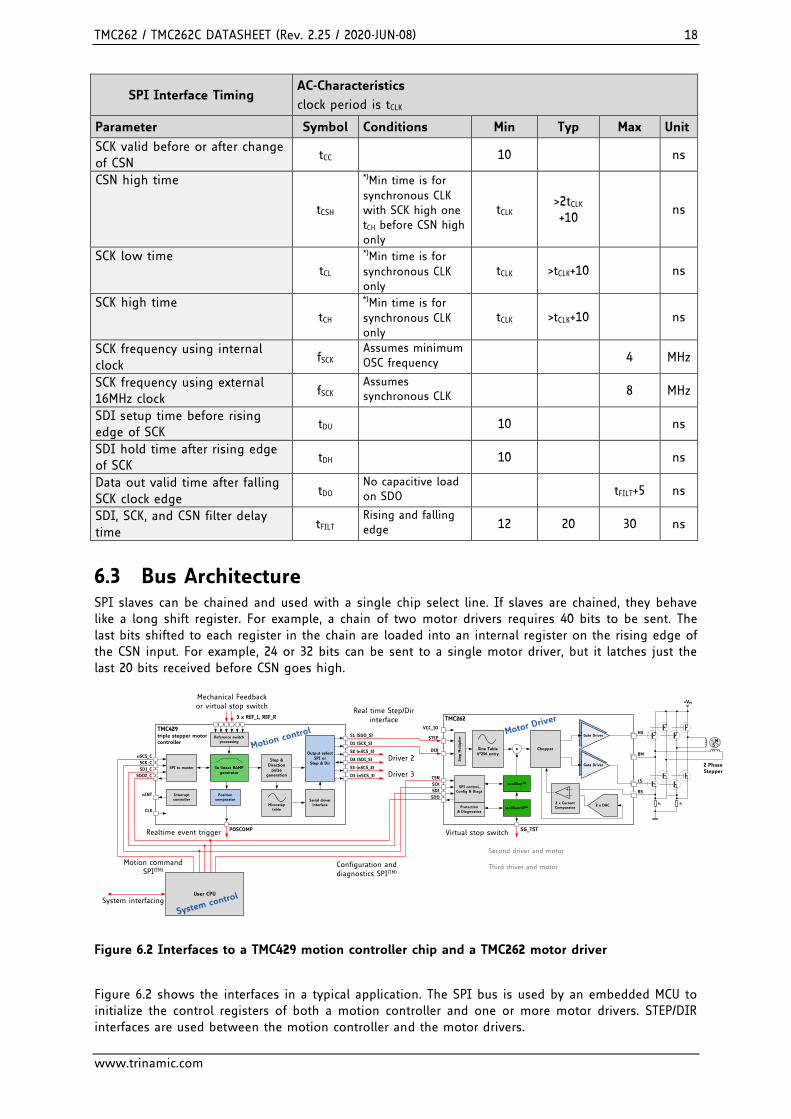
6.3 Bus Architecture SPI slaves can be chained and used with a single chip select line. If slaves are chained, they behave like a long shift register. For example, a chain of two motor drivers requires 40 bits to be sent. The last bits shifted to each register in the chain are loaded into an internal register on the rising edge of the CSN input. For example, 24 or 32 bits can be sent to a single motor driver, but it latches just the last 20 bits received before CSN goes high.
Driver 3
STEP
DIR
CSN
SCK
SDO
SDI
VCC_IOTMC429 triple stepper motor controller
SPI to master
nSCS_C
SCK_C
SDOZ_C
SDI_C
CLK
3x linear RAMP generator
Position comparator
Interruptcontroller
nINT
Reference switch processing
Step & Direction
pulse generation
Output selectSPI or
Step & Dir
Microstep table
Serial driver interface
POSCOMP
3 x REF_L, REF_R
S1 (SDO_S)
D1 (SCK_S)
S2 (nSCS_S)
D2 (SDI_S)
S3 (nSCS_2)
D3 (nSCS_3)
Driver 2
Real time Step/Dir interface
User CPU
Motion command SPI(TM)
Configuration and diagnostics SPI(TM)
Mechanical Feedback or virtual stop switch
Realtime event trigger Virtual stop switch
Third driver and motor
Second driver and motor
System interfacing
System control
Motion control
Gate driver
Gate driverGate Driver
Gate Driver
2 x Current Comparator
TMC262
Protection& Diagnostics
Sine Table4*256 entry
2 x DAC
SPI control,Config & Diags
stallGuard2™
coolStep™
x
Ste
p M
ultip
lier
SG_TST
Chopper
+VM
HS
LS
2 Phase Stepper
NS
BM
RS RS
RS
Motor Driver
Figure 6.2 Interfaces to a TMC429 motion controller chip and a TMC262 motor driver
Figure 6.2 shows the interfaces in a typical application. The SPI bus is used by an embedded MCU to initialize the control registers of both a motion controller and one or more motor drivers. STEP/DIR interfaces are used between the motion controller and the motor drivers.
TMC262 / TMC262C DATASHEET (Rev. 2.25 / 2020-JUN-08) 19
www.trinamic.com
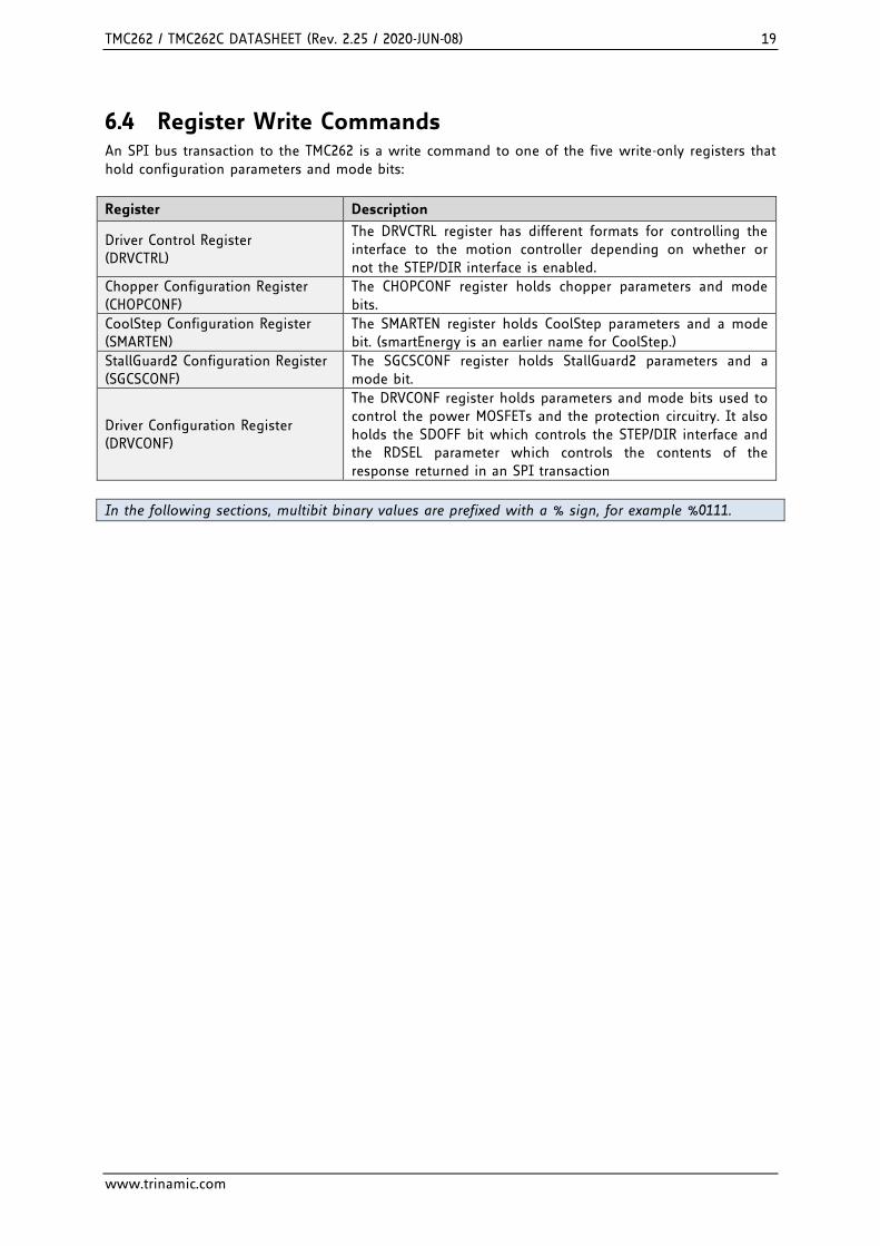
6.4 Register Write Commands An SPI bus transaction to the TMC262 is a write command to one of the five write-only registers that hold configuration parameters and mode bits:
Register Description
Driver Control Register (DRVCTRL)
The DRVCTRL register has different formats for controlling the interface to the motion controller depending on whether or not the STEP/DIR interface is enabled.
Chopper Configuration Register (CHOPCONF)
The CHOPCONF register holds chopper parameters and mode bits.
CoolStep Configuration Register (SMARTEN)
The SMARTEN register holds CoolStep parameters and a mode bit. (smartEnergy is an earlier name for CoolStep.)
StallGuard2 Configuration Register (SGCSCONF)
The SGCSCONF register holds StallGuard2 parameters and a mode bit.
Driver Configuration Register (DRVCONF)
The DRVCONF register holds parameters and mode bits used to control the power MOSFETs and the protection circuitry. It also holds the SDOFF bit which controls the STEP/DIR interface and the RDSEL parameter which controls the contents of the response returned in an SPI transaction
In the following sections, multibit binary values are prefixed with a % sign, for example %0111.

TMC262 / TMC262C DATASHEET (Rev. 2.25 / 2020-JUN-08) 20
www.trinamic.com
6.4.1 Write Command Overview The table below shows the formats for the five register write commands. Bits 19, 18, and sometimes 17 select the register being written, as shown in bold. The DRVCTRL register has two formats, as selected by the SDOFF bit. Bits shown as 0 must always be written as 0, and bits shown as 1 must always be written with 1. Detailed descriptions of each parameter and mode bit are given in the following sections.
Register/
Bit
DRVCTRL
(SDOFF=1)
DRVCTRL
(SDOFF=0)
CHOPCONF
SMARTEN
SGCSCONF DRVCONF
19 0 0 1 1 1 1
18 0 0 0 0 1 1
17 PHA 0 0 1 0 1
16 CA7 0 TBL1 0 SFILT TST
15 CA6 0 TBL0 SEIMIN 0 SLPH1
14 CA5 0 CHM SEDN1 SGT6 SLPH0
13 CA4 0 RNDTF SEDN0 SGT5 SLPL1
12 CA3 0 HDEC1 0 SGT4 SLPL0
11 CA2 0 HDEC0 SEMAX3 SGT3 0
10 CA1 0 HEND3 SEMAX2 SGT2 DISS2G
9 CA0 INTPOL HEND2 SEMAX1 SGT1 TS2G1
8 PHB DEDGE HEND1 SEMAX0 SGT0 TS2G0
7 CB7 0 HEND0 0 0 SDOFF
6 CB6 0 HSTRT2 SEUP1 0 VSENSE
5 CB5 0 HSTRT1 SEUP0 0 RDSEL1
4 CB4 0 HSTRT0 0 CS4 RDSEL0
3 CB3 MRES3 TOFF3 SEMIN3 CS3 OTSENS *)
2 CB2 MRES2 TOFF2 SEMIN2 CS2 SHRTSENS *)
1 CB1 MRES1 TOFF1 SEMIN1 CS1 0
0 CB0 MRES0 TOFF0 SEMIN0 CS0 EN_S2VS *)
*) Additional option for TMC262C only. Setting these bits for TMC262 does not have any effect.
6.4.2 Read Response Overview The table below shows the formats for the read response. The RDSEL parameter in the DRVCONF register selects the format of the read response.
Bit RDSEL=%00 RDSEL=%01 RDSEL=%10
19 MSTEP9 SG9 SG9
18 MSTEP8 SG8 SG8
17 MSTEP7 SG7 SG7
16 MSTEP6 SG6 SG6
15 MSTEP5 SG5 SG5
14 MSTEP4 SG4 SE4
13 MSTEP3 SG3 SE3
12 MSTEP2 SG2 SE2
11 MSTEP1 SG1 SE1
10 MSTEP0 SG0 SE0
9 - - -
8 - - -
7 STST
6 OLB
5 OLA
4 S2GB
3 S2GA
2 OTPW
1 OT
0 SG

TMC262 / TMC262C DATASHEET (Rev. 2.25 / 2020-JUN-08) 21
www.trinamic.com
6.5 Driver Control Register (DRVCTRL) The format of the DRVCTRL register depends on the state of the SDOFF mode bit. SPI Mode SDOFF bit is set, the STEP/DIR interface is disabled, and DRVCTRL is the interface for
specifying the currents through each coil.
STEP/DIR Mode SDOFF bit is clear, the STEP/DIR interface is enabled, and DRVCTRL is a configuration register for the STEP/DIR interface.
6.5.1 DRVCTRL Register in SPI Mode
DRVCTRL Driver Control in SPI Mode (SDOFF=1)
Bit Name Function Comment
19 0 Register address bit
18 0 Register address bit
17 PHA Polarity A Sign of current flow through coil A: 0: Current flows from OA1 pins to OA2 pins. 1: Current flows from OA2 pins to OA1 pins.
16 CA7 Current A MSB Magnitude of current flow through coil A. The range is 0 to 248, if hysteresis or offset are used up to their full extent. The resulting value after applying hysteresis or offset must not exceed 255.
15 CA6
14 CA5
13 CA4
12 CA3
11 CA2
10 CA1
9 CA0 Current A LSB
8 PHB Polarity B Sign of current flow through coil B: 0: Current flows from OB1 pins to OB2 pins. 1: Current flows from OB2 pins to OB1 pins.
7 CB7 Current B MSB Magnitude of current flow through coil B. The range is 0 to 248, if hysteresis or offset are used up to their full extent. The resulting value after applying hysteresis or offset must not exceed 255.
6 CB6
5 CB5
4 CB4
3 CB3
2 CB2
1 CB1
0 CB0 Current B LSB

TMC262 / TMC262C DATASHEET (Rev. 2.25 / 2020-JUN-08) 22
www.trinamic.com
6.5.2 DRVCTRL Register in STEP/DIR Mode
DRVCTRL Driver Control in STEP/DIR Mode (SDOFF=0)
Bit Name Function Comment
19 0 Register address bit
18 0 Register address bit
17 0 Reserved
16 0 Reserved
15 0 Reserved
14 0 Reserved
13 0 Reserved
12 0 Reserved
11 0 Reserved
10 0 Reserved
9 INTPOL Enable STEP interpolation
0: Disable STEP pulse interpolation. 1: Enable MicroPlyer STEP pulse multiplication by 16.
8 DEDGE Enable double edge STEP pulses
0: Rising STEP pulse edge is active, falling edge is inactive. 1: Both rising and falling STEP pulse edges are active.
7 0 Reserved
6 0 Reserved
5 0 Reserved
4 0 Reserved
3 MRES3 Microstep resolution for STEP/DIR mode
Microsteps per 90°: %0000: 256 %0001: 128 %0010: 64 %0011: 32 %0100: 16 %0101: 8 %0110: 4 %0111: 2 (halfstep) %1000: 1 (fullstep)
2 MRES2
1 MRES1
0 MRES0

TMC262 / TMC262C DATASHEET (Rev. 2.25 / 2020-JUN-08) 23
www.trinamic.com
6.6 Chopper Control Register (CHOPCONF)
CHOPCONF Chopper Configuration
Bit Name Function Comment
19 1 Register address bit
18 0 Register address bit
17 0 Register address bit
16 TBL1 Blanking time Blanking time interval, in system clock periods: %00: 16 %01: 24 %10: 36 %11: 54
15 TBL0
14 CHM Chopper mode This mode bit affects the interpretation of the HDEC, HEND, and HSTRT parameters shown below.
0 Standard mode (SpreadCycle)
1
Constant tOFF with fast decay time. Fast decay time is also terminated when the negative nominal current is reached. Fast decay is after on time.
13 RNDTF Random TOFF time Enable randomizing the slow decay phase duration: 0: Chopper off time is fixed as set by bits tOFF 1: Random mode, tOFF is random modulated by dNCLK= -12 … +3 clocks.
12 HDEC1 Hysteresis decrement interval or Fast decay mode
CHM=0
Hysteresis decrement period setting, in system clock periods: %00: 16 %01: 32 %10: 48 %11: 64
11 HDEC0
CHM=1 HDEC1=0: current comparator can terminate the fast decay phase before timer expires. HDEC1=1: only the timer terminates the fast decay phase.
HDEC0: MSB of fast decay time setting.
10 HEND3 Hysteresis end (low) value or Sine wave offset
CHM=0
%0000 … %1111: Hysteresis is -3, -2, -1, 0, 1, …, 12 (1/512 of this setting adds to current setting) This is the hysteresis value which becomes used for the hysteresis chopper.
9 HEND2
8 HEND1 CHM=1 %0000 … %1111: Offset is -3, -2, -1, 0, 1, …, 12 This is the sine wave offset and 1/512 of the value becomes added to the absolute value of each sine wave entry.
7 HEND0
6 HSTRT2 Hysteresis start value or Fast decay time setting
CHM=0
Hysteresis start offset from HEND: %000: 1 %100: 5 %001: 2 %101: 6 %010: 3 %110: 7 %011: 4 %111: 8 Effective: HEND+HSTRT must be ≤ 15
5 HSTRT1
4 HSTRT0
CHM=1 Three least-significant bits of the duration of the fast decay phase. The MSB is HDEC0. Fast decay time is a multiple of system clock periods: NCLK= 32 x (HDEC0+HSTRT)

TMC262 / TMC262C DATASHEET (Rev. 2.25 / 2020-JUN-08) 24
www.trinamic.com
CHOPCONF Chopper Configuration
Bit Name Function Comment
3 TOFF3 Off time/MOSFET disable
Duration of slow decay phase. If TOFF is 0, the MOSFETs are shut off. If TOFF is nonzero, slow decay time is a multiple of system clock periods: NCLK= 24 + (32 x TOFF) (Minimum time is 64clocks.) %0000: Driver disable, all bridges off %0001: 1 (use with TBL of minimum 24 clocks) %0010 … %1111: 2 … 15
2 TOFF2
1 TOFF1
0 TOFF0
6.7 CoolStep Control Register (SMARTEN)
SMARTEN CoolStep Configuration
Bit Name Function Comment
19 1 Register address bit
18 0 Register address bit
17 1 Register address bit
16 0 Reserved
15 SEIMIN Minimum CoolStep current
0: ½ CS current setting 1: ¼ CS current setting
14 SEDN1 Current decrement speed
Number of times that the StallGuard2 value must be sampled equal to or above the upper threshold for each decrement of the coil current: %00: 32 %01: 8 %10: 2 %11: 1
13 SEDN0
12 0 Reserved
11 SEMAX3 Upper CoolStep threshold as an offset from the lower threshold
If the StallGuard2 measurement value SG is sampled equal to or above (SEMIN+SEMAX+1) x 32 enough times, then the coil current scaling factor is decremented.
10 SEMAX2
9 SEMAX1
8 SEMAX0
7 0 Reserved
6 SEUP1 Current increment size
Number of current increment steps for each time that the StallGuard2 value SG is sampled below the lower threshold: %00: 1 %01: 2 %10: 4 %11: 8
5 SEUP0
4 0 Reserved
3 SEMIN3 Lower CoolStep threshold/CoolStep disable
If SEMIN is 0, CoolStep is disabled. If SEMIN is nonzero and the StallGuard2 value SG falls below SEMIN x 32, the CoolStep current scaling factor is increased.
2 SEMIN2
1 SEMIN1
0 SEMIN0
TMC262 / TMC262C DATASHEET (Rev. 2.25 / 2020-JUN-08) 25
www.trinamic.com
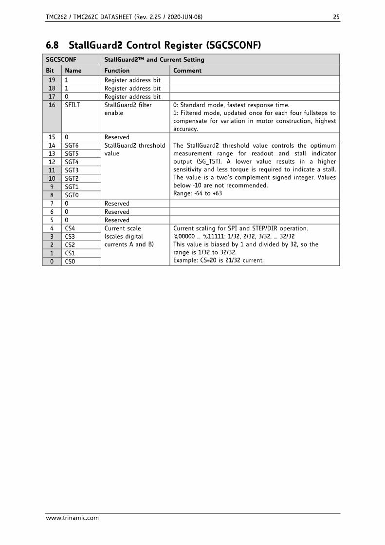
6.8 StallGuard2 Control Register (SGCSCONF)
SGCSCONF StallGuard2™ and Current Setting
Bit Name Function Comment
19 1 Register address bit
18 1 Register address bit
17 0 Register address bit
16 SFILT StallGuard2 filter enable
0: Standard mode, fastest response time. 1: Filtered mode, updated once for each four fullsteps to compensate for variation in motor construction, highest accuracy.
15 0 Reserved
14 SGT6 StallGuard2 threshold value
The StallGuard2 threshold value controls the optimum measurement range for readout and stall indicator output (SG_TST). A lower value results in a higher sensitivity and less torque is required to indicate a stall. The value is a two’s complement signed integer. Values below -10 are not recommended. Range: -64 to +63
13 SGT5
12 SGT4
11 SGT3
10 SGT2
9 SGT1
8 SGT0
7 0 Reserved
6 0 Reserved
5 0 Reserved
4 CS4 Current scale (scales digital currents A and B)
Current scaling for SPI and STEP/DIR operation. %00000 … %11111: 1/32, 2/32, 3/32, … 32/32 This value is biased by 1 and divided by 32, so the range is 1/32 to 32/32. Example: CS=20 is 21/32 current.
3 CS3
2 CS2
1 CS1
0 CS0

TMC262 / TMC262C DATASHEET (Rev. 2.25 / 2020-JUN-08) 26
www.trinamic.com
6.9 Driver Control Register (DRVCONF)
DRVCONF Driver Configuration
Bit Name Function Comment
19 1 Register address bit
18 1 Register address bit
17 1 Register address bit
16 TST Reserved TEST mode Must be cleared for normal operation. When set, the SG_TST output exposes digital test values, and the TEST_ANA output exposes analog test values. Test value selection is controlled by SGT1 and SGT0: TEST_ANA: %00: anatest_2vth,
%01: anatest_dac_out, %10: anatest_vdd_half.
SG_TST: %00: comp_A, %01: comp_B, %10: CLK, %11: on_state_xy
15 SLPH1 Slope control, high side
%00: Minimum %01: Minimum (+tc) %10: Medium (+tc) %11: Maximum In temperature compensated mode (tc), the high-side MOSFET gate driver strength is increased if the overtemperature warning temperature is reached. This compensates for temperature dependency of high-side slope control.
14 SLPH0
13 SLPL1 Slope control, low side 12 SLPL0
11 0 Reserved
10 DISS2G Short to GND protection disable
0: Short to GND protection is enabled. 1: Short to GND protection is disabled.
9 TS2G1 Short to GND detection timer
%00: 3.2µs. %01: 1.6µs. %10: 1.2µs. %11: 0.8µs.
8 TS2G0
7 SDOFF STEP/DIR interface disable
0: Enable STEP/DIR operation. 1: Disable STEP/DIR operation. SPI interface is used to move motor.
6 VSENSE Sense resistor voltage-based current scaling
0: Full-scale sense resistor voltage is 310mV. 1: Full-scale sense resistor voltage is 165mV. (Full-scale refers to a current setting of 31 and a DAC value of 255.)
5 RDSEL1 Select value for read out (RD bits)
%00 Microstep position read back
4 RDSEL0 %01 StallGuard2 level read back
%10 StallGuard2 & CoolStep current level read back
%11 Reserved, do not use
3 OTSENS *)
Overtemperature sensitivity
0: Shutdown at 150°C 1: Sensitive shutdown at 136°C
2 SHRTSENS *)
Short to GND detection sensitivity
0: Low sensitivity 1: High sensitivity – better protection for high side FETs
1 0 Reserved
0 EN_S2VS *)
Enable short to VS & CLK fail protection
0: Short to VS and clock failsafe protection disabled 1: Short to VS / overcurrent protection enabled. In addition, enables protection against clock input CLK fail, when using an external clock source.
*) These three bits have a function for TMC262C only. Setting these bits for TMC262 does not have any effect. The TMC262 and TMC262C behave identically with setting 0.
TMC262 / TMC262C DATASHEET (Rev. 2.25 / 2020-JUN-08) 27
www.trinamic.com
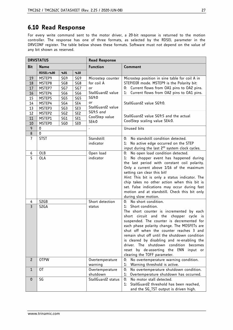
6.10 Read Response For every write command sent to the motor driver, a 20-bit response is returned to the motion controller. The response has one of three formats, as selected by the RDSEL parameter in the DRVCONF register. The table below shows these formats. Software must not depend on the value of any bit shown as reserved.
DRVSTATUS Read Response
Bit Name Function Comment
RDSEL=%00 %01 %10
19 MSTEP9 SG9 SG9 Microstep counter for coil A or StallGuard2 value SG9:0 or StallGuard2 value SG9:5 and CoolStep value SE4:0
Microstep position in sine table for coil A in STEP/DIR mode. MSTEP9 is the Polarity bit: 0: Current flows from OA1 pins to OA2 pins. 1: Current flows from OA2 pins to OA1 pins.
18 MSTEP8 SG8 SG8
17 MSTEP7 SG7 SG7
16 MSTEP6 SG6 SG6
15 MSTEP5 SG5 SG5 StallGuard2 value SG9:0.
14 MSTEP4 SG4 SE4
13 MSTEP3 SG3 SE3
12 MSTEP2 SG2 SE2 StallGuard2 value SG9:5 and the actual CoolStep scaling value SE4:0.
11 MSTEP1 SG1 SE1
10 MSTEP0 SG0 SE0
9 0 - Unused bits
8 0
7 STST Standstill indicator
0: No standstill condition detected. 1: No active edge occurred on the STEP input during the last 220 system clock cycles.
6 OLB Open load indicator
0: No open load condition detected. 1: No chopper event has happened during the last period with constant coil polarity. Only a current above 1/16 of the maximum setting can clear this bit! Hint: This bit is only a status indicator. The chip takes no other action when this bit is set. False indications may occur during fast motion and at standstill. Check this bit only during slow motion.
5 OLA
4 S2GB Short detection status
0: No short condition. 1: Short condition. The short counter is incremented by each short circuit and the chopper cycle is suspended. The counter is decremented for each phase polarity change. The MOSFETs are shut off when the counter reaches 3 and remain shut off until the shutdown condition is cleared by disabling and re-enabling the driver. The shutdown condition becomes reset by de-asserting the ENN input or clearing the TOFF parameter.
3 S2GA
2 OTPW Overtemperature warning
0: No overtemperature warning condition. 1: Warning threshold is active.
1 OT Overtemperature shutdown
0: No overtemperature shutdown condition. 1: Overtemperature shutdown has occurred.
0 SG StallGuard2 status 0: No motor stall detected. 1: StallGuard2 threshold has been reached,
and the SG_TST output is driven high.

TMC262 / TMC262C DATASHEET (Rev. 2.25 / 2020-JUN-08) 28
www.trinamic.com
6.11 Device Initialization The following sequence of SPI commands is an example of enabling the driver and initializing the chopper:
SPI = $901B4; // Hysteresis mode or
SPI = $94557; // Constant toff mode
SPI = $D001F; // Current setting: $d001F (max. current)
SPI = $EF010; // high gate driver strength, StallGuard read, SDOFF=0
SPI = $00000; // 256 microstep setting First test of CoolStep current control:
SPI = $A0222; // Enable CoolStep with minimum current ½ CS
The configuration parameters should be tuned to the motor and application for optimum performance.
TMC262 / TMC262C DATASHEET (Rev. 2.25 / 2020-JUN-08) 29
www.trinamic.com
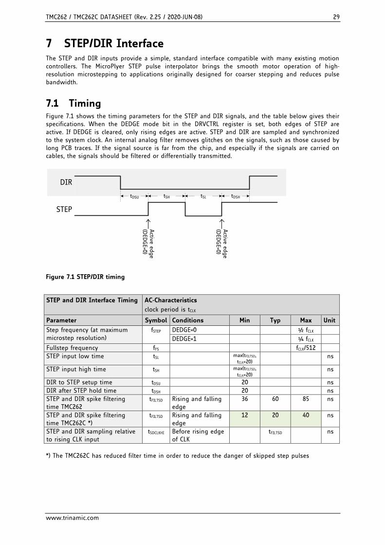
7 STEP/DIR Interface The STEP and DIR inputs provide a simple, standard interface compatible with many existing motion controllers. The MicroPlyer STEP pulse interpolator brings the smooth motor operation of high-resolution microstepping to applications originally designed for coarser stepping and reduces pulse bandwidth.
7.1 Timing Figure 7.1 shows the timing parameters for the STEP and DIR signals, and the table below gives their specifications. When the DEDGE mode bit in the DRVCTRL register is set, both edges of STEP are active. If DEDGE is cleared, only rising edges are active. STEP and DIR are sampled and synchronized to the system clock. An internal analog filter removes glitches on the signals, such as those caused by long PCB traces. If the signal source is far from the chip, and especially if the signals are carried on cables, the signals should be filtered or differentially transmitted.
DIR
STEP
tDSHtSH tSLtDSU
Active ed
ge
(DED
GE=0)
Active ed
ge
(DED
GE=0)
Figure 7.1 STEP/DIR timing
STEP and DIR Interface Timing AC-Characteristics
clock period is tCLK
Parameter Symbol Conditions Min Typ Max Unit
Step frequency (at maximum microstep resolution)
fSTEP DEDGE=0 ½ fCLK
DEDGE=1 ¼ fCLK
Fullstep frequency fFS fCLK/512
STEP input low time tSL max(tFILTSD, tCLK+20)
ns
STEP input high time tSH max(tFILTSD, tCLK+20)
ns
DIR to STEP setup time tDSU 20 ns
DIR after STEP hold time tDSH 20 ns
STEP and DIR spike filtering time TMC262
tFILTSD Rising and falling edge
36 60 85 ns
STEP and DIR spike filtering time TMC262C *)
tFILTSD Rising and falling edge
12 20 40 ns
STEP and DIR sampling relative to rising CLK input
tSDCLKHI Before rising edge of CLK
tFILTSD ns
*) The TMC262C has reduced filter time in order to reduce the danger of skipped step pulses

TMC262 / TMC262C DATASHEET (Rev. 2.25 / 2020-JUN-08) 30
www.trinamic.com
7.2 Microstep Table The internal microstep table maps the sine function from 0° to 90°, and symmetries allow mapping the sine and cosine functions from 0° to 360° with this table. The angle is encoded as a 10-bit unsigned integer MSTEP provided by the microstep counter. The size of the increment applied to the counter while microstepping through this table is controlled by the microstep resolution setting MRES in the DRVCTRL register. Depending on the DIR input, the microstep counter is increased (DIR=0) or decreased (DIR=1) by the step size with each STEP active edge. Despite many entries in the last quarter of the table being equal, the electrical angle continuously changes, because either the sine wave or cosine wave is in an area, where the current vector changes monotonically from position to position. Figure 7.2 shows the table. The largest values are 248, which leaves headroom used for adding an offset.
Entry 0-31 32-63 64-95 96-127 128-159 160-191 192-223 224-255
0 1 49 96 138 176 207 229 243
1 2 51 97 140 177 207 230 244
2 4 52 98 141 178 208 231 244
3 5 54 100 142 179 209 231 244
4 7 55 101 143 180 210 232 244
5 8 57 103 145 181 211 232 245
6 10 58 104 146 182 212 233 245
7 11 60 105 147 183 212 233 245
8 13 61 107 148 184 213 234 245
9 14 62 108 150 185 214 234 246
10 16 64 109 151 186 215 235 246
11 17 65 111 152 187 215 235 246
12 19 67 112 153 188 216 236 246
13 21 68 114 154 189 217 236 246
14 22 70 115 156 190 218 237 247
15 24 71 116 157 191 218 237 247
16 25 73 118 158 192 219 238 247
17 27 74 119 159 193 220 238 247
18 28 76 120 160 194 220 238 247
19 30 77 122 161 195 221 239 247
20 31 79 123 163 196 222 239 247
21 33 80 124 164 197 223 240 247
22 34 81 126 165 198 223 240 248
23 36 83 127 166 199 224 240 248
24 37 84 128 167 200 225 241 248
25 39 86 129 168 201 225 241 248
26 40 87 131 169 201 226 241 248
27 42 89 132 170 202 226 242 248
28 43 90 133 172 203 227 242 248
29 45 91 135 173 204 228 242 248
30 46 93 136 174 205 228 243 248
31 48 94 137 175 206 229 243 248
Figure 7.2 Internal microstep table showing the first quarter of the sine wave
TMC262 / TMC262C DATASHEET (Rev. 2.25 / 2020-JUN-08) 31
www.trinamic.com
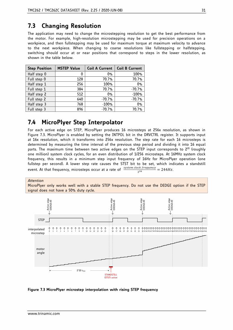
7.3 Changing Resolution The application may need to change the microstepping resolution to get the best performance from the motor. For example, high-resolution microstepping may be used for precision operations on a workpiece, and then fullstepping may be used for maximum torque at maximum velocity to advance to the next workpiece. When changing to coarse resolutions like fullstepping or halfstepping, switching should occur at or near positions that correspond to steps in the lower resolution, as shown in the table below.
Step Position MSTEP Value Coil A Current Coil B Current
Half step 0 0 0% 100%
Full step 0 128 70.7% 70.7%
Half step 1 256 100% 0%
Full step 1 384 70.7% -70.7%
Half step 2 512 0% -100%
Full step 2 640 -70.7% -70.7%
Half step 3 768 -100% 0%
Full step 3 896 -70.7% 70.7%
7.4 MicroPlyer Step Interpolator For each active edge on STEP, MicroPlyer produces 16 microsteps at 256x resolution, as shown in Figure 7.3. MicroPlyer is enabled by setting the INTPOL bit in the DRVCTRL register. It supports input at 16x resolution, which it transforms into 256x resolution. The step rate for each 16 microsteps is determined by measuring the time interval of the previous step period and dividing it into 16 equal parts. The maximum time between two active edges on the STEP input corresponds to 220 (roughly one million) system clock cycles, for an even distribution of 1/256 microsteps. At 16MHz system clock frequency, this results in a minimum step input frequency of 16Hz for MicroPlyer operation (one fullstep per second). A lower step rate causes the STST bit to be set, which indicates a standstill
event. At that frequency, microsteps occur at a rate of 𝑠𝑦𝑠𝑡𝑒𝑚 𝑐𝑙𝑜𝑐𝑘 𝑓𝑟𝑒𝑞𝑢𝑒𝑛𝑐𝑦
216 = 244𝐻𝑧.
Attention MicroPlyer only works well with a stable STEP frequency. Do not use the DEDGE option if the STEP signal does not have a 50% duty cycle.
STEP
interpolated microstep
Act
ive e
dge
(DED
GE=
0)
Act
ive e
dge
(DED
GE=
0)
Act
ive e
dge
(DED
GE=
0)
0 1 2 3 4 5 6 7 8 9 10 11 12 13 14 15 16 17 18 19 20 21 22 23 32
Act
ive e
dge
(DED
GE=
0)
STANDSTILL (STST) active
33 34 35 36 37 38 39 40 41 42 43 44 45 46 47 48 49 50
motorangle
52 53 54 55 56 57 58 59 60 61 62 63 64 65 6651
2^20 tCLK
Figure 7.3 MicroPlyer microstep interpolation with rising STEP frequency
TMC262 / TMC262C DATASHEET (Rev. 2.25 / 2020-JUN-08) 32
www.trinamic.com
In Figure 7.3, the first STEP cycle is long enough to set the STST bit. This bit is cleared on the next STEP active edge. Then, the STEP frequency increases and after one cycle at the higher rate MicroPlyer increases the interpolated microstep rate. During the last cycle at the slower rate, MicroPlyer did not generate all 16 microsteps, so there is a tiny jump in motor angle between the first and second cycles at the higher rate.
7.5 Standstill Current Reduction When a standstill event is detected, the motor current should be reduced to save energy and to reduce heat dissipation in the power MOSFET stage. Especially halfstep positions are worst-case for motor and driver with regard to the distribution of the power dissipation, because the full energy is consumed in one bridge and one motor coil.
Hint Implement a current reduction to 10% to 75% of the required run current for motor standstill. This saves more than 50% to more than 90% of energy. The actual level depends on the required holding force and on the required microstep precision during standstill. In standalone mode, a reduction to
50% current is possible using a configuration input.

TMC262 / TMC262C DATASHEET (Rev. 2.25 / 2020-JUN-08) 33
www.trinamic.com
8 Current Setting The internal 5V supply voltage available at the pin 5VOUT is used as a reference for the coil current regulation based on the sense resistor voltage measurement. The desired maximum motor current is set by selecting an appropriate value for the sense resistor. The sense resistor voltage range can be selected by the VSENSE bit in the DRVCONF register. The low sensitivity (high sense resistor voltage, VSENSE=0) brings best and most robust current regulation, while high sensitivity (low sense resistor voltage, VSENSE=1) reduces power dissipation in the sense resistor. This setting reduces the power dissipation in the sense resistor by nearly half. After choosing the VSENSE setting and selecting the sense resistor, the currents to both coils are scaled by the 5-bit current scale parameter CS in the SGCSCONF register. The sense resistor value is chosen so that the maximum desired current (or slightly more) flows at the maximum current setting (CS = %11111). Using the internal sine wave table, which has amplitude of 248, the RMS motor current can be calculated by:
𝐼𝑅𝑀𝑆 =𝐶𝑆 + 1
32∗
𝑉𝐹𝑆
𝑅𝑆𝐸𝑁𝑆𝐸
∗1
√2
The momentary motor current is calculated as:
𝐼𝑀𝑂𝑇 =𝐶𝑈𝑅𝑅𝐸𝑁𝑇𝐴/𝐵
248∗
𝐶𝑆 + 1
32∗
𝑉𝐹𝑆
𝑅𝑆𝐸𝑁𝑆𝐸
where: CS is the effective current scale setting as set by the CS bits and modified by CoolStep. The effective value ranges from 0 to 31.
VFS is the sense resistor voltage at full scale, as selected by the VSENSE control bit (refer to the electrical characteristics). CURRENTA/B is the value set by the current setting in SPI mode or the internal sine table in STEP/DIR mode.
Parameter Description Setting Comment
CS Current scale. Scales both coil current values as taken from the internal sine wave table or from the SPI interface. For high precision motor operation, work with a current scaling factor in the range 16 to 31, because scaling down the current values reduces the effective microstep resolution by making microsteps coarser. This setting also controls the maximum current value set by CoolStep™.
0 … 31 Scaling factor: 1/32, 2/32, … 32/32
VSENSE Allows control of the sense resistor voltage range or adaptation of one electronic module to different maximum motor currents.
0 310mV
1 165mV

TMC262 / TMC262C DATASHEET (Rev. 2.25 / 2020-JUN-08) 34
www.trinamic.com
8.1 Sense Resistors Sense resistors should be carefully selected. The full motor current flows through the sense resistors. As they also see the switching spikes from the MOSFET bridges, a low-inductance type such as film or composition resistors is required to prevent spikes causing ringing. A compact power stage layout with massive GND plane for low-inductance and low-resistance is essential to avoid disturbance by parasitic effects. Any common GND path for the two sense resistors must be avoided, because this would lead to coupling between the two current sense signals. Use the massive ground plane for all GND connections. When using high currents or long motor cables, spike damping with parallel capacitors to ground may be needed, as shown in Figure 8.1. Because the sense resistor inputs are susceptible to damage from negative overvoltages, an additional input protection resistor helps protect against a motor cable break or ringing on long motor cables.
SRA
RSENSE
SRB
RSENSE
10R to 47R
10R to 47R
optional input protection resistors
MOSFET bridge
MOSFET bridge
GNDTMC262 Power
supply GND
no common GND path not visible to TMC262470nF
470nFoptional filter
capacitors
Figure 8.1 Sense resistor grounding and protection components
The sense resistor needs to be able to conduct the peak motor coil current in motor standstill conditions, unless standby power is reduced. Under normal conditions, the sense resistor sees less than 50% of the coil RMS current, because no current flows through the sense resistor during the slow decay phases. The peak sense resistor power dissipation is:
𝑃𝑅𝑆𝑀𝐴𝑋 =(𝑉𝑆𝐸𝑁𝑆𝐸 ∗
𝐶𝑆 + 132
)2
𝑅𝑆𝐸𝑁𝑆𝐸
For high-current applications, halve power dissipation by using the lower sense resistor voltage setting and the corresponding lower resistance value. Set the desired maximum motor current by selecting an appropriate value for the sense resistor. The following table shows the RMS current values which are reached using standard resistors. The resulting application current may vary due to slow decay phase effects and trace resistance.
CHOICE OF RSENSE AND RESULTING MAX. MOTOR CURRENT FOR CS=31
RSENSE [Ω] RMS current [A] VSENSE=0 RMS current [A] VSENSE=1
0.33 0.7 0.35
0.27 0.8 0.43
0.22 1.0 0.53
0.15 1.5 0.8
0.12 1.8 1.0
0.10 2.2 1.2
0.075 3 1.6
0.066 3.3 1.8
0.050 4.4 2.3

TMC262 / TMC262C DATASHEET (Rev. 2.25 / 2020-JUN-08) 35
www.trinamic.com
9 Chopper Operation The currents through both motor coils are controlled using choppers. The choppers work independently of each other. Figure 9.1 shows the three chopper phases:
RSENSE
ICOIL
On Phase: current flows in direction of target current
RSENSE
ICOIL
Fast Decay Phase: current flows in opposite direction of target current
RSENSE
ICOIL
Slow Decay Phase: current re-circulation
+VM +VM +VM
Figure 9.1 Chopper phases
Although the current could be regulated using only on phases and fast decay phases, insertion of the slow decay phase is important to reduce electrical losses and current ripple in the motor. The duration of the slow decay phase is specified in a control parameter and sets an upper limit on the chopper frequency. The current comparator can measure coil current during phases when the current flows through the sense resistor, but not during the slow decay phase, so the slow decay phase is terminated by a timer. The on phase is terminated by the comparator when the current through the coil reaches the target current. The fast decay phase may be terminated by either the comparator or another timer. When the coil current is switched, spikes at the sense resistors occur due to charging and discharging parasitic capacitances. During this time, typically one or two microseconds, the current cannot be measured. Blanking is the time when the input to the comparator is masked to block these spikes. There are two chopper modes available: a new high-performance chopper algorithm called SpreadCycle and a proven constant off-time chopper mode. The constant off-time mode cycles through three phases: on, fast decay, and slow decay. The SpreadCycle mode cycles through four phases: on, slow decay, fast decay, and a second slow decay. Three parameters are used for controlling both chopper modes:
Parameter Description Setting Comment
TOFF Off time. This setting controls the duration of the slow decay time and limits the maximum chopper frequency. For most applications an off time within the range of 5µs to 20µs will fit. If the value is 0, the MOSFETs are all shut off and the motor can freewheel. A value of 1 to 15 sets the number of system clock cycles in the slow decay phase to:
𝑁𝐶𝐿𝐾 = (𝑇𝑂𝐹𝐹 ∙ 32) + 12 The SD-Time is
𝑡 = 1
𝑓𝐶𝐿𝐾∙ 𝑁𝐶𝐿𝐾
0 Chopper off.
1… 15 Off time setting. A setting in the range of 2-5 is recommended for SpreadCycle, higher values for classic chopper.

TMC262 / TMC262C DATASHEET (Rev. 2.25 / 2020-JUN-08) 36
www.trinamic.com
Parameter Description Setting Comment
TBL Blanking time. This time needs to cover the switching event and the duration of the ringing on the sense resistor. For most low-current applications, a setting of 16 or 24 is good. For high-current applications, a setting of 36 or 54 may be required.
0 16 system clock cycles
1 24 system clock cycles
2 36 system clock cycles
3 54 system clock cycles
CHM Chopper mode bit 0 SpreadCycle mode
1 Constant off time mode
9.1 SpreadCycle Chopper The SpreadCycle (patented) chopper algorithm is a precise and simple to use chopper mode which automatically determines the optimum length for the fast-decay phase. The SpreadCycle will provide superior microstepping quality even with default settings. Several parameters are available to optimize the chopper to the application. Each chopper cycle is comprised of an on phase, a slow decay phase, a fast decay phase and a second slow decay phase (see Figure 9.4). The two slow decay phases and the two blank times per chopper cycle put an upper limit to the chopper frequency. The slow decay phases typically make up for about 30%-70% of the chopper cycle in standstill and are important for low motor and driver power dissipation. Calculation of a starting value for the slow decay time TOFF:
EXAMPLE: Target Chopper frequency: 25kHz. Assumption: Two slow decay cycles make up for 50% of overall chopper cycle time
𝑡𝑂𝐹𝐹 =1
25𝑘𝐻𝑧∗
50
100∗
1
2= 10µ𝑠
For the TOFF setting this means: 𝑇𝑂𝐹𝐹 = (𝑡𝑂𝐹𝐹 ∗ 𝑓𝐶𝐿𝐾 − 24)/32
With 12 MHz clock this gives a setting of TOFF=3.0, i.e. 3. With 16 MHz clock this gives a setting of TOFF=4.25, i.e. 4 or 5.
The hysteresis start setting forces the driver to introduce a minimum amount of current ripple into the motor coils. The current ripple must be higher than the current ripple which is caused by resistive losses in the motor in order to give best microstepping results. This will allow the chopper to precisely regulate the current both for rising and for falling target current. The time required to introduce the current ripple into the motor coil also reduces the chopper frequency. Therefore, a higher hysteresis setting will lead to a lower chopper frequency. The motor inductance limits the ability of the chopper to follow a changing motor current. Further the duration of the on phase and the fast decay must be longer than the blanking time, because the current comparator is disabled during blanking. It is easiest to find the best setting by starting from a low hysteresis setting (e.g. HSTRT=0, HEND=0) and increasing HSTRT, until the motor runs smoothly at low velocity settings. This can best be checked when measuring the motor current either with a current probe or by probing the sense resistor voltages (see Figure 9.2). Checking the sine wave shape near zero transition will show a small ledge between both half waves in case the hysteresis setting is too small. At medium velocities (i.e. 100 to 400 fullsteps per second), a too low hysteresis setting will lead to increased humming and vibration of the motor.
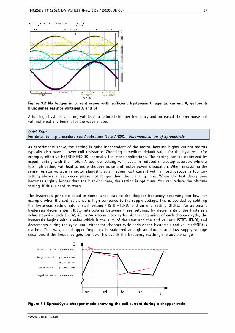
TMC262 / TMC262C DATASHEET (Rev. 2.25 / 2020-JUN-08) 37
www.trinamic.com
Figure 9.2 No ledges in current wave with sufficient hysteresis (magenta: current A, yellow & blue: sense resistor voltages A and B)
A too high hysteresis setting will lead to reduced chopper frequency and increased chopper noise but will not yield any benefit for the wave shape.
Quick Start For detail tuning procedure see Application Note AN001 - Parameterization of SpreadCycle
As experiments show, the setting is quite independent of the motor, because higher current motors typically also have a lower coil resistance. Choosing a medium default value for the hysteresis (for example, effective HSTRT+HEND=10) normally fits most applications. The setting can be optimized by experimenting with the motor: A too low setting will result in reduced microstep accuracy, while a too high setting will lead to more chopper noise and motor power dissipation. When measuring the sense resistor voltage in motor standstill at a medium coil current with an oscilloscope, a too low setting shows a fast decay phase not longer than the blanking time. When the fast decay time becomes slightly longer than the blanking time, the setting is optimum. You can reduce the off-time setting, if this is hard to reach. The hysteresis principle could in some cases lead to the chopper frequency becoming too low, for example when the coil resistance is high compared to the supply voltage. This is avoided by splitting the hysteresis setting into a start setting (HSTRT+HEND) and an end setting (HEND). An automatic hysteresis decrementer (HDEC) interpolates between these settings, by decrementing the hysteresis value stepwise each 16, 32, 48, or 64 system clock cycles. At the beginning of each chopper cycle, the hysteresis begins with a value which is the sum of the start and the end values (HSTRT+HEND), and decrements during the cycle, until either the chopper cycle ends or the hysteresis end value (HEND) is reached. This way, the chopper frequency is stabilized at high amplitudes and low supply voltage situations, if the frequency gets too low. This avoids the frequency reaching the audible range.
t
I
target current
target current - hysteresis start
target current + hysteresis start
on sd fd sd
target current + hysteresis end
target current - hysteresis end
HDEC
Figure 9.3 SpreadCycle chopper mode showing the coil current during a chopper cycle

TMC262 / TMC262C DATASHEET (Rev. 2.25 / 2020-JUN-08) 38
www.trinamic.com
Three parameters control SpreadCycle mode:
Parameter Description Setting Comment
HSTRT Hysteresis start setting. Please remark, that this value is an offset to the hysteresis end value HEND.
0… 7 This setting adds to HEND. %000: 1 %100: 5 %001: 2 %101: 6 %010: 3 %110: 7 %011: 4 %111: 8
HEND Hysteresis end setting. Sets the hysteresis end value after a number of decrements. Decrement interval time is controlled by HDEC. The sum HSTRT+HEND must be <16. At a current setting CS of max. 30 (amplitude reduced to 240), the sum is not limited.
0… 2 Negative HEND: -3… -1 %0000: -3 %0001: -2 %0010: -1
3 Zero HEND: 0 %0011: 0
4… 15 Positive HEND: 1… 12 %0100: 1 %1010: 7 1100: 9 %0101: 2 %1011: 8 1101: 10 %0110: 3 %1100: 9 1110: 11 %0111: 4 %1101: 10 %1000: 5 %1110: 11 %1001: 6 %1111: 12
HDEC Hysteresis decrement setting. This setting determines the slope of the hysteresis during on time and during fast decay time. It sets the number of system clocks for each decrement.
0… 3 0: fast decrement 3: very slow decrement
%00: 16 %01: 32 %10: 48 %11: 64
EXAMPLE: A hysteresis of 4 has been chosen. You might decide to not use hysteresis decrement. In this case set: HEND=6 (sets an effective end value of 6-3=3) HSTRT=0 (sets minimum hysteresis, i.e. 1: 3+1=4) In order to take advantage of the variable hysteresis, we can set most of the value to the HSTRT, i.e. 4, and the remaining 1 to hysteresis end. The resulting configuration register values are as follows: HEND=0 (sets an effective end value of -3) HSTRT=6 (sets an effective start value of hysteresis end +7: 7-3=4)
Hint Highest motor velocities benefit from setting TOFF to 2 or 3 and a short TBL of 2 or 1.

TMC262 / TMC262C DATASHEET (Rev. 2.25 / 2020-JUN-08) 39
www.trinamic.com
9.2 Classic Constant Off-Time Chopper The classic constant off-time chopper uses a fixed-time fast decay following each on phase. While the duration of the on phase is determined by the chopper comparator, the fast decay time needs to be fast enough for the driver to follow the falling slope of the sine wave, but it should not be so long that it causes excess motor current ripple and power dissipation. This can be tuned using an oscilloscope or evaluating motor smoothness at different velocities. A good starting value is a fast decay time setting similar to the slow decay time setting.
t
I
mean value = target current
target current + offset
on sdfd sdon fd
Figure 9.4 Constant off-time chopper with offset showing the coil current during two cycles
After tuning the fast decay time, the offset should be tuned for a smooth zero crossing. This is necessary because the fast decay phase makes the absolute value of the motor current lower than the target current (see Figure 9.5). If the zero offset is too low, the motor stands still for a short moment during current zero crossing. If it is set too high, it makes a larger microstep. Typically, a positive offset setting is required for smoothest operation.
t
ITarget current
Coil current
t
ITarget current
Coil current
Coil current does not have optimum shape Target current corrected for optimum shape of coil current
Figure 9.5 Zero crossing with correction using sine wave offset

TMC262 / TMC262C DATASHEET (Rev. 2.25 / 2020-JUN-08) 40
www.trinamic.com
Three parameters control constant off-time mode:
Parameter Description Setting Comment
TFD (HSTART & HDEC0)
Fast decay time setting. With CHM=1, these bits control the portion of fast decay for each chopper cycle.
0 Slow decay only.
1… 15 Duration of fast decay phase.
OFFSET (HEND)
Sine wave offset. With CHM=1, these bits control the sine wave offset. A positive offset corrects for zero crossing error.
0…2 Negative offset: -3… -1
3 No offset: 0
4… 15 Positive offset: 1… 12
NCCFD (HDEC1)
Selects usage of the current comparator for termination of the fast decay cycle. If current comparator is enabled, it terminates the fast decay cycle in case the current reaches a higher negative value than the actual positive value.
0 Enable comparator termination of fast decay cycle.
1 End by time only.
9.2.1 Random Off Time In the constant off-time chopper mode, both coil choppers run freely without synchronization. The frequency of each chopper mainly depends on the coil current and the motor coil inductance. The inductance varies with the microstep position. With some motors, a slightly audible beat can occur between the chopper frequencies when they are close together. This typically occurs at a few microstep positions within each quarter wave. This effect is usually not audible when compared to mechanical noise generated by ball bearings, etc. Another factor which can cause a similar effect is a poor layout of the sense resistor GND connections.
Hint A common cause of motor noise is a bad PCB layout causing coupling of both sense resistor
voltages. Noise caused by an insufficient PCB layout cannot be overcome by chopper settings.
To minimize the effect of a beat between both chopper frequencies, an internal random generator is provided. It modulates the slow decay time setting when switched on by the RNDTF bit. The RNDTF feature further spreads the chopper spectrum, reducing electromagnetic emission on single frequencies.
Parameter Description Setting Comment
RNDTF Enables a random off-time generator, which slightly modulates the off-time tOFF using a random polynomial.
0 Disable.
1 Random modulation enabled.

TMC262 / TMC262C DATASHEET (Rev. 2.25 / 2020-JUN-08) 41
www.trinamic.com
10 Power MOSFET Stage The TMC262 provides gate drivers for two full-bridges using N- and P-channel power MOSFETs. The gate current for the MOSFETs can be adapted to influence the slew rate at the coil outputs. The main features of the stage are:
- 5V gate drive voltage for low-side N-MOS transistors, 8V-10V for high-side P-MOS transistors.
- The gate drivers protect the bridges actively against cross-conduction using an internal QGD protection that holds the MOSFETs safely off.
- Automatic break-before-make logic minimizes dead time and diode-conduction time.
- Integrated short to ground protection detects a short of the motor wires and protects the MOSFETs.
The low-side gate driver is supplied by the 5VOUT pin. The low-side driver supplies 0V to the MOSFET gate to close the MOSFET, and 5VOUT to open it. The high-side gate driver voltage is supplied by the VS and the VHS pin. VHS is more negative than VS and allows opening the VS referenced high-side MOSFET. The high-side driver supplies VS to the P channel MOSFET gate to close the MOSFET and VHS to open it. The effective low-side gate voltage is roughly 5V; the effective high-side gate voltage is roughly 8V, respectively 10V for TMC262C.
Parameter Description Setting Comment
SLPL Low-side slope control. Controls the MOSFET gate driver current. Set to a value appropriate for the external MOSFET gate charge and the desired slope.
0… 3 %00: Minimum. %01: Minimum. %10: Medium. %11: Maximum.
SLPH High-side slope control. Controls the MOSFET gate driver current. Set to a value appropriate for the external MOSFET gate charge and the desired slope.
0… 3 %00: Minimum. %01: Minimum+TC. %10: Medium+TC. %11: Maximum.
10.1 Break-Before-Make Logic Each half-bridge has to be protected against cross-conduction during switching events. When switching off the low-side MOSFET, its gate first needs to be discharged before the high-side MOSFET is allowed to switch on. The same goes when switching off the high-side MOSFET and switching on the low-side MOSFET. The time for charging and discharging of the MOSFET gates depends on the MOSFET gate charge and the gate driver current set by SLPL and SLPH. The BBM (break-before-make) logic measures the gate voltage and automatically delays turning on the opposite bridge transistor until its counterpart is discharged. This way, the bridge will always switch with optimized timing independent of the slope setting.
10.2 ENN Input The MOSFETs can be completely disabled in hardware by pulling the ENN input high. This allows the motor to free-wheel. An equivalent function can be performed in software by setting the parameter TOFF to zero. The hardware disable is available for allowing the motor to be hot plugged. If a hardware disable function is not needed, tie ENN low.
10.3 Slope Control The TMC262 provides constant-current gate drivers for slope control. This allows adapting the driver strength to the drive requirements of the power MOSFETs and adjusting the output slope of the controlled gate charge and discharge. A slower slope reduces electromagnetic emissions, but it increases power dissipation in the MOSFETs.

TMC262 / TMC262C DATASHEET (Rev. 2.25 / 2020-JUN-08) 42
www.trinamic.com
The duration of the complete switching event depends on the total gate charge of the MOSFETs. In Figure 10.1, the voltage transition of the gate-charge output (dotted line) takes place during the so-called Miller plateau. The Miller plateau results from the gate-to-drain capacitance of the MOSFET charging or discharging during switching. The datasheet for the MOSFETs typically will show a Miller plateau that only covers a part (for example, one quarter) of the complete charging/discharging event. The gate voltage level at which the Miller plateau starts depends on the threshold voltage of the MOSFET and on the actual load current.
MOSFET gate charge vs. switching event
QG – Total gate charge (nC)
VGS –
Gat
e to
sourc
e vo
ltag
e (V
)
5
4
3
2
1
00 2 4 6 8 10
VDS –
Dra
in to s
ourc
e vo
ltag
e (V
)
25
20
15
10
5
0
VS
QMILLER
Figure 10.1 MOSFET gate charge vs. VDS for a typical MOSFET during a switching event
The slope time tSLOPE can be calculated as:
𝑡𝑆𝐿𝑂𝑃𝐸 =𝑄𝑀𝐼𝐿𝐿𝐸𝑅
𝐼𝐺𝐴𝑇𝐸
Where: QMILLER is the charge the MOSFET needs for the switching event.
IGATE is the driver current setting. The chopper frequency is typically slightly above the audible range, around 18 kHz to 40 kHz. The lower limit for the slope is dictated by the reverse recovery time of the MOSFET internal diodes, unless additional Schottky diodes are used in parallel to the MOSFETs source-drain diode. For most applications a switching time between 20ns and 250ns is best. Example:
A circuit using the transistor in Figure 10.1 is operated with a gate current setting of 15mA. The Miller charge of the transistor is about 2.5nC.
𝑡𝑆𝐿𝑂𝑃𝐸 = 2.5𝑛𝐶
15𝑚𝐴= 166𝑛𝑠
Hint Test the best driver strength setting in the application. A good value is found, if a further increment of driver strength does not lead to lower supply current (and thus reduced power dissipation).

TMC262 / TMC262C DATASHEET (Rev. 2.25 / 2020-JUN-08) 43
www.trinamic.com
11 Diagnostics and Protection
11.1 Short Protection The TMC262 protects the MOSFET power stages against a short circuit or overload condition by monitoring the voltage drop in the high-side MOSFETs (Figure 11.1). The TMC262C also allows monitoring the voltage drop in sense resistor and low-side MOSFETs. A programmable short detection delay (shortdelay) allows adjusting the detector to work with different power stages and load conditions. Additionally, the short detection is protected against single events, e.g. caused by ESD discharges, by retrying three times before switching off the motor continuously. The low side short detector provides a good overcurrent detection. It needs to be explicitly enabled by programming. The short detection status is indicated by two bits:
Status Description Range Comment
S2GA These bits identify a short to GND condition on coil A and coil B persisting for multiple chopper cycles. The bits are cleared when the MOSFETs are disabled. For TMC262C, a short detected on the low-side also is signaled by these bits.
0 / 1 0: No short detected. 1: Short condition
detected. S2GB
An overload condition on the high-side MOSFET (“short to GND”) is detected by monitoring the coil voltage during the high-side on phase. Under normal conditions, the high-side power MOSFET reaches the bridge supply voltage minus a small voltage drop during the on-phase. If the bridge is overloaded, the voltage cannot rise to the detection level within the time defined by the internal detection delay setting. When an overload is detected, the bridge is switched off. The short to GND detection delay needs to be adjusted for the slope time, because it must be longer than slope, but should not be unnecessarily long.
Short detection
Valid areaBMxy
Hxy
VVS-VBMS2G
0V
0V
VVS
tS2G
BM voltage monitored
Short to GND monitor phase
Driver enabled
0V
tS2G
Short detecteddelaydelay inactiveinactive
Short to GND detected
Driver off
Figure 11.1 Short to GND detection timing
TMC262C allows short to supply detection in the same way, by measuring voltage drop across sense resistors plus low-side MOSFETs during the conduction phase. As the low-side short detection includes the sense resistor, it is sensitive to the actual sense resistor and provides a good precision of overcurrent detection. This way, it will safely cover most overcurrent conditions. For compatibility, short to VS protection is disabled by default.

TMC262 / TMC262C DATASHEET (Rev. 2.25 / 2020-JUN-08) 44
www.trinamic.com
The short detector is controlled by a mode bit and a parameter:
Mode bit / Parameter
Description Setting Comment
DISS2G Short to ground detection disable bit. 0/1 0: Short to ground detection enabled
1: Short to ground detection disabled
TS2G This setting controls the short detection delay time. It needs to cover the switching slope time. A higher setting reduces sensitivity to capacitive loads.
0… 3 %00: 3.2µs. %01: 1.6µs. %10: 1.2µs. %11: 0.8µs.
EN_S2VS (TMC262C, only)
Explicitly enable short to VS and overcurrent protection by setting this bit.
0/1 Enable detection for normal use (1).
SHRTSENS (TMC262C, only)
The high-side overcurrent detector can be set to a higher sensitivity by setting this flag. This will allow detection of wrong cabling even with higher resistive motors.
0/1 0: Low sensitivity 1: High sensitivity
Hint Once a short condition is safely detected, the corresponding driver bridge (A or B) becomes switched off, and the s2ga or s2gb flag becomes set. To restart the motor, disable and re-enable the driver.
Attention Short protection cannot protect the system and the power stages for all possible short events, as a short event is rather undefined and a complex network of external components may be involved. Therefore, short circuits should basically be avoided.
11.2 Open-Load Detection Interrupted cables are a common cause for systems failing, e.g. when connectors are not firmly plugged. The TMC2590 detects open load conditions by checking, if it can reach the desired motor coil current. This way, also undervoltage conditions, high motor velocity settings or short and overtemperature conditions may cause triggering of the open load flag, and inform the user, that motor torque may suffer. In motor stand still, open load cannot be measured, as the coils might eventually have zero current.
Hint Open load detection is provided for system debugging. Open load detection does not necessarily indicate a malfunction of the driver. In order to safely detect an interrupted coil connection, read out the open load flags at low or nominal motor velocity operation, only. However, the ola and olb flags have just informative character and do not cause any action of the driver. False indication may result with full- or halfstep operation. Use microstepping for a safe result.
The open-load detection status is indicated by two bits:
Status flag Description Range Comment
OLA These bits indicate an open-load condition on coil A and coil B. The flags become set, if no chopper event has happened during the last period with constant coil polarity. The flag is not updated with too low actual coil current below 1/16 of maximum setting. It is a pure indicator. No action is taken depending on these flags.
0 / 1 0: No open-load detected
1: Open-load detected
OLB
TMC262 / TMC262C DATASHEET (Rev. 2.25 / 2020-JUN-08) 45
www.trinamic.com
11.3 Temperature Sensors The TMC262 integrates a two-level temperature sensor (100°C warning and 150°C shutdown) for diagnostics and for protection of the power MOSFETs. The temperature detector can be triggered by heat accumulation on the board, for example due to missing convection cooling. Most critical situations, in which the MOSFETs could be overheated, are avoided when using the short protection. For most applications, the overtemperature warning indicates an abnormal operation situation and can be used to trigger an alarm or power-reduction measures. If continuous operation in hot environments is necessary, a more precise mechanism based on temperature measurement should be used. The thermal shutdown is strictly an emergency measure and temperature rising to the shutdown level should be prevented by design. The shutdown temperature is above the specified operating temperature range of the chip.
Hint for TMC262C, only After triggering the overtemperature sensor (ot flag), the driver remains switched off until the system temperature falls below the overtemperature release level (120°C) to avoid continuous heating to the shutdown level. Cool down typically needs a few 100ms to 1 second.
The high-side P-channel gate drivers have a temperature dependency which can be compensated to some extent by increasing the gate driver current when the warning temperature threshold is reached. The chip automatically corrects for the temperature dependency above the warning temperature when the temperature-compensated modes of SLPH is used. In these modes, the gate driver current is increased by one step when the temperature warning threshold is reached.
11.4 Undervoltage Detection The undervoltage detector monitors both the internal logic supply voltage and the supply voltage. It prevents operation of the chip when the MOSFETs cannot be guaranteed to operate properly because the gate drive voltage is too low. It also initializes the chip at power up. In undervoltage conditions, the logic control block becomes reset and the driver is disabled. All MOSFETs are switched off. All internal registers are reset to zero. Software also should monitor the supply voltage to detect an undervoltage condition. If software cannot measure the supply voltage, an undervoltage condition can be detected when the response to an SPI command returns only zero bits in the response and no bits are shifted through the internal shift register from SDI to SDO. After a reset due to undervoltage occurs, the CS parameter is cleared, which is reflected in an SE status of 0 in the read response.
Status Description Range Comment
OTPW Overtemperature warning. This bit indicates whether the warning threshold is reached. Software can react to this setting by reducing current.
0 / 1 1: temperature prewarning level reached
OT Overtemperature shutdown. This bit indicates whether the shutdown threshold has been reached and the driver has been disabled.
0 / 1 1: driver shut down due to over-temperature
OTSENS (TMC262C only)
Program overtemperature threshold to a reduced level in order to give better protection for the external power stage and other components. The driver re-enables when the temperature falls below 120°C.
0 / 1 0: 150°C 1: 136°C

TMC262 / TMC262C DATASHEET (Rev. 2.25 / 2020-JUN-08) 46
www.trinamic.com
Time
VVS
Device in reset: all registers cleared to 0
Reset
VUV
ca. 100µs ca. 100µs
Figure 11.2 Undervoltage reset timing
Note Be sure to operate the IC significantly above the undervoltage threshold to ensure reliable operation! Check for SE reading back as zero to detect an undervoltage event.
12 Power Supply Sequencing The TMC262 generates its own 5V supply for all internal operations. The internal reset of the chip is derived from the supply voltage regulator in order to ensure a clean start-up of the device after power up. During start up, the SPI unit is in reset and cannot be addressed. All registers become cleared. VCC_IO limits the voltage allowable on the inputs and outputs and is used for driving the outputs, but input levels thresholds are not depending on the actual level of VCC_IO. VCC_IO may start up before or after VS. However, with a delayed start-up of VCC_IO, care must be taken for systems using an external clock signal (see next chapter). For TMC262C, VCC_IO is monitored, and the IC becomes reset upon undervoltage. This way, the power-up restriction for VCC_IO with external clock signal is relaxed.

TMC262 / TMC262C DATASHEET (Rev. 2.25 / 2020-JUN-08) 47
www.trinamic.com
13 System Clock The system clock is the timing reference for all functions. The internal system clock frequency for all operations is nominally 15MHz. An external clock of 8MHz to 20MHz can be supplied for more exact timing, especially when using CoolStep and StallGuard2.
USING THE INTERNAL CLOCK
To use the on-chip oscillator of the TMC262, tie CLK to GND near the chip. The actual on-chip oscillator clock frequency can be determined by measuring the delay time between the last step and assertion of the STST (standstill) status bit, which is 220 clocks. There is some delay in reading the STST bit through the SPI interface, but it is easily possible to measure the oscillator frequency within 1%. Chopper timing parameters can then be corrected using this measurement, because the oscillator is relatively stable over a wide range of environmental temperatures.
Hint In case well defined precise motor chopper operation are desired, it is supposed to work with an external clock source.
USING EXTERNAL CLOCK
An external clock frequency of up to 20MHz can be supplied (up to 16MHz for first batch of TMC262C, production date 1837). It is recommended to use an external clock frequency between 10MHz and 16MHz for best performance. Pay attention to using a near 50% duty-cycle. The external clock is enabled and the on-chip oscillator is disabled with the first logic high driven on the CLK input.
Attention: Never leave the external clock input floating. It is not allowed to remain within the transition region (between valid low and high levels), as spurious clock signals might lead to short impulses and can corrupt internal logic state. Provide an external pull-down resistor, in case the driver pin (i.e. microcontroller output) does not provide a safe level directly after power up. If the external clock is suspended or disabled after the internal oscillator has been disabled, the chip will not operate. Be careful to switch off the power MOSFETs (by driving the ENN input high or setting the TOFF parameter to 0) before switching off the clock, because otherwise the chopper would stop and the motor current level could rise uncontrolled. If the short to GND detection is enabled, it stays active even without clock. The TMC262C provides a clock failover option to switch back to internal clock, in case of the external clock failing. The function is coupled to enabling short to VS protection (EN_S2VS).
Status Description Range Comment
EN_S2VS Set this bit to enable protection against a failing external CLK source. If set, the IC switches back to external clock after 32 to 48 internal clock cycles. At the same time, this bit controls the higher side short detector sensitivity
0 / 1 Undervoltage level 0: Stopping clock will
stop the IC. 1: CLK fail safe
protection

TMC262 / TMC262C DATASHEET (Rev. 2.25 / 2020-JUN-08) 48
www.trinamic.com
Time
VVS
Device in reset: all registers cleared to 0
VUV
VVCC_IO
max. VCC_IO
Device in reset: all registers cleared to 0
Defined clock, no intermediate levels allowedC
LK m
ust
be
low
, w
hile
VCC_I
O is
belo
w V
INHI
VINHI
3.3V/5V
Operation, CLK is not allowed to have undefined levels between VINLO and VINHI and timing must
satisfy TCLK (min)
VCLK
Figure 13.1 Start-up requirements of CLK input
13.1 Frequency Selection A higher frequency allows faster step rates, faster SPI operation, and higher chopper frequencies. On the other hand, it may cause more electromagnetic emission and more power dissipation in the digital logic. Generally, a system clock frequency of 10MHz to 16MHz is best for most applications, unless the motor is to operate at the highest velocities. If the application can tolerate reduced motor velocity and increased chopper noise, a clock frequency of 4MHz to 10MHz should be considered.
CLK frequency Comment
internal 13-16MHz, typical. Tie clock input firmly to GND. See electrical characteristics for limits. The internal clock is sufficient, unless a good reproducibility of StallGuard values is desired.
4-10 MHz Lower range sufficient for higher inductance motors
10-16 MHz Recommended for best results
16-20 MHz Option in case a lower frequency is not available Ensure 40-60% duty cycle
>14 MHz Attention for TMC262C, date code 1837 only: Minimum high-level time of 27ns is required for switching to external clock. Ensure min. 45% duty cycle of CLK signal up to 16Mhz. > 16MHz not recommended.

TMC262 / TMC262C DATASHEET (Rev. 2.25 / 2020-JUN-08) 49
www.trinamic.com
14 TMC262C compatibility The TMC262C is a new derivative of the TMC262 family. It is designed for compatibility to existing applications, while offering a number of enhancements and options, which can be activated using the interface. Care has been taken to ensure compatibility for both devices, even if the enhanced options are switched on.
ENHANCEMENTS IN TMC262C
• More silent chopper operation, silent motor at low motor velocity.
• VCC_IO is monitored by internal reset circuitry to ensure clean power-up and power-down.
• Overtemperature shutdown has added hysteresis, to avoid spurious switching off. Following overtemperature, the driver stage remains switched off until the IC cools down below 120°C.
• Increased drive-level for P-MOSMETs for lower power dissipation in the external power-stage.
• Reduced power dissipation of internal circuitry, leading to lower heat-up.
• CMOS input levels are increased with 5V VCC_IO level to increase noise rejection.
• Reduced filtering time for STEP & DIR inputs to reduce the risk of missed step pulses.
OPTIONAL ENHANCEMENTS IN TMC262C (ENABLE VIA CONFIGURATION BITS)
• Clock fail-safe option. In case the external clock fails, the IC defaults back to internal clock. This avoids damage to motor and driver stage. (Enable: EN_S2VS, together with short protection)
• Low-Side short detection (Short to VS). The low-side short detector provides improved robustness in case of mis-wiring or wrongly attached motor. (Enable: EN_S2VS)
• Optional higher sensitivity high-side protection. Especially in combination with low-RDSon MOSFETs, this feature gives a better protection. (Enable: SHRTSENS)
• Optional lower overtemperature threshold of 136°C for more sensitive protection of the power driver. Enable: OTSENSE
The additional settings for TMC262C are highlighted in this document using green background.
The major differences to be considered when exchanging the TMC262 and TMC262C, are summed up in the following table:
Item Change in TMC262C Impact
More silent chopper with TMC262C
Internal noise sources have been reduced. Noise caused by internal wiring voltage drop makes up for up to 10mV within the TMC262. This reflects in a slightly lower sense input threshold voltage.
Reduced motor noise, especially with low velocity. TMC262C effective motor current about 2-3% higher.
Undervoltage monitoring of VCC_IO
IO voltage VCC_IO is monitored by the internal reset circuitry. The device becomes reset upon VCC_IO undervoltage.
Increased VCC_IO supply current (50µA), device resets upon VCC_IO undervoltage.
Hysteresis for overtemperature detector
Following overtemperature detection at 136°C or 150°C, the driver stage remains switched off until the IC cools down below 120°C.
Longer shutdown time upon overtemperature detection, safe detection by interface.
Increased P-MOS drive level
The drive level for the P-MOS has been increased from roughly 8V to 10V.
Reduced heat up of driver FETs.
Input levels depend on VCC_IO voltage
TMC262 input level detectors are supplied by internal 5V supply, leading to fixed 0.8V and 2.4V levels. TMC262C uses VCC_IO supplied CMOS Schmitt-Trigger inputs instead.
Higher positive logic level for 5V VCC_IO supply. No change with 3.3V VCC_IO supply. Check levels in 5V systems.
Spike filtering time on STEP/DIR input
The filtering has been improved, while reducing the filtering time in order to reduce the risk of missing short step pulses.
Potential impact in systems with high noise level on STEP & DIR input pins.
CLK input filter TMC262C provides better filtering against short pulses (10ns typ.). Attention: Date code 1837 requires>27ns high level for switching to ext. CLK
Increased robustness against reflections on CLK line.
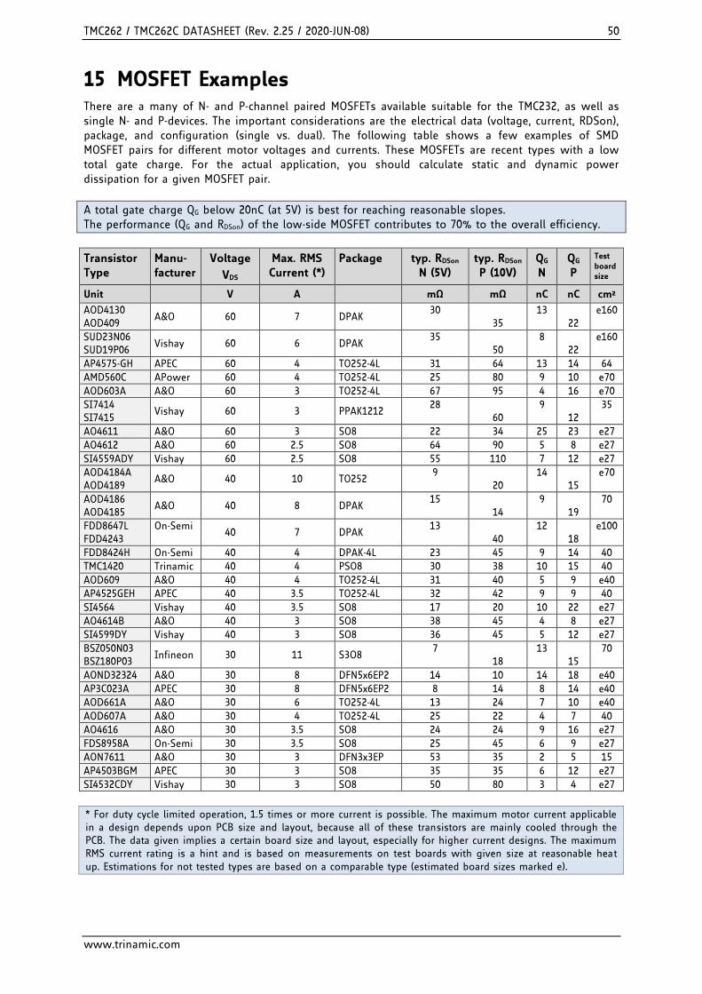
TMC262 / TMC262C DATASHEET (Rev. 2.25 / 2020-JUN-08) 50
www.trinamic.com
15 MOSFET Examples There are a many of N- and P-channel paired MOSFETs available suitable for the TMC232, as well as single N- and P-devices. The important considerations are the electrical data (voltage, current, RDSon), package, and configuration (single vs. dual). The following table shows a few examples of SMD MOSFET pairs for different motor voltages and currents. These MOSFETs are recent types with a low total gate charge. For the actual application, you should calculate static and dynamic power dissipation for a given MOSFET pair.
A total gate charge QG below 20nC (at 5V) is best for reaching reasonable slopes. The performance (QG and RDSon) of the low-side MOSFET contributes to 70% to the overall efficiency.
Transistor Type
Manu-facturer
Voltage
VDS
Max. RMS Current (*)
Package typ. RDSon N (5V)
typ. RDSon P (10V)
QG N
QG P
Test board size
Unit V A mΩ mΩ nC nC cm²
AOD4130 AOD409
A&O 60 7 DPAK 30
35 13
22
e160
SUD23N06 SUD19P06
Vishay 60 6 DPAK 35
50 8
22
e160
AP4575-GH APEC 60 4 TO252-4L 31 64 13 14 64
AMD560C APower 60 4 TO252-4L 25 80 9 10 e70
AOD603A A&O 60 3 TO252-4L 67 95 4 16 e70
SI7414 SI7415
Vishay 60 3 PPAK1212 28
60 9
12 35
AO4611 A&O 60 3 SO8 22 34 25 23 e27
AO4612 A&O 60 2.5 SO8 64 90 5 8 e27
SI4559ADY Vishay 60 2.5 SO8 55 110 7 12 e27
AOD4184A AOD4189
A&O 40 10 TO252 9
20 14
15
e70
AOD4186 AOD4185
A&O 40 8 DPAK 15
14 9
19
70
FDD8647L FDD4243
On-Semi 40 7 DPAK
13 40
12 18
e100
FDD8424H On-Semi 40 4 DPAK-4L 23 45 9 14 40
TMC1420 Trinamic 40 4 PSO8 30 38 10 15 40
AOD609 A&O 40 4 TO252-4L 31 40 5 9 e40
AP4525GEH APEC 40 3.5 TO252-4L 32 42 9 9 40
SI4564 Vishay 40 3.5 SO8 17 20 10 22 e27
AO4614B A&O 40 3 SO8 38 45 4 8 e27
SI4599DY Vishay 40 3 SO8 36 45 5 12 e27
BSZ050N03 BSZ180P03
Infineon 30 11 S3O8 7
18 13
15
70
AOND32324 A&O 30 8 DFN5x6EP2 14 10 14 18 e40
AP3C023A APEC 30 8 DFN5x6EP2 8 14 8 14 e40
AOD661A A&O 30 6 TO252-4L 13 24 7 10 e40
AOD607A A&O 30 4 TO252-4L 25 22 4 7 40
AO4616 A&O 30 3.5 SO8 24 24 9 16 e27
FDS8958A On-Semi 30 3.5 SO8 25 45 6 9 e27
AON7611 A&O 30 3 DFN3x3EP 53 35 2 5 15
AP4503BGM APEC 30 3 SO8 35 35 6 12 e27
SI4532CDY Vishay 30 3 SO8 50 80 3 4 e27
* For duty cycle limited operation, 1.5 times or more current is possible. The maximum motor current applicable in a design depends upon PCB size and layout, because all of these transistors are mainly cooled through the PCB. The data given implies a certain board size and layout, especially for higher current designs. The maximum RMS current rating is a hint and is based on measurements on test boards with given size at reasonable heat up. Estimations for not tested types are based on a comparable type (estimated board sizes marked e).

TMC262 / TMC262C DATASHEET (Rev. 2.25 / 2020-JUN-08) 51
www.trinamic.com
16 Layout Considerations The PCB layout is critical to good performance, because the environment includes both high-sensitivity analog signals and high-current motor drive signals. A massive GND plane is required for good results, both for heat conduction as well as electrical.
16.1 Sense Resistors The sense resistors are susceptible to ground differences and ground ripple voltage, as the microstep current steps result in voltages down to 0.5mV. Each sense resistor should have an individual and short connection to the GND plane. Place the sense resistors close to the power MOSFETs with one or more vias to the ground plane for each sense resistor. This also helps to keep harmful parasitic inductance small. The sense resistor layout is also sensitive to coupling between the axes. The two sense resistors should not share a common ground connection trace or vias, because PCB traces have some resistance. A symmetrical layout for both fullbridges on both sides of the TMC262 makes it easiest to ensure symmetry as well as minimum coupling and disturbance between both coil current regulators.
16.2 Exposed Die Pad The exposed die pad and all GND pins must be connected to a solid ground plane spreading heat into the board and providing for a stable GND reference. All signals of the TMC262 are referenced to GND. Directly connect all GND pins to a common ground area.
16.3 Power Filtering The 470nF to 10µF (6.3V, min.) ceramic filtering capacitor on 5VOUT should be placed as close as possible to the 5VOUT pin, with its GND return going directly to the nearest GND pin. Use as short and as thick connections as possible. A 100nF filtering capacitor should be placed as close as possible from the VS pin to the ground plane. The motor MOSFET bridge supply pins should be decoupled with an electrolytic (>47 μF is recommended) capacitor and a ceramic capacitor, placed close to the device. Take into account that the switching motor coil outputs have a high dV/dt, and thus capacitive stray into high resistive signals can occur, if the motor traces are near other traces over longer distances.
16.4 Thermal Resistance For the QFN-32, a thermal resistance of roughly 35°C/W Rthja can be expected with a thermally optimized design (12-16 vias to GND plane). As the TMC262 does not have much power dissipation, a few vias (4 recommended) for the GND plane are enough. This will give a higher thermal resistance of roughly 50-70°C/W.
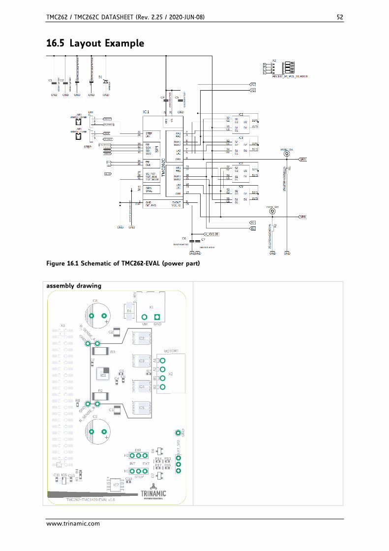
TMC262 / TMC262C DATASHEET (Rev. 2.25 / 2020-JUN-08) 52
www.trinamic.com
16.5 Layout Example
Figure 16.1 Schematic of TMC262-EVAL (power part)
assembly drawing

TMC262 / TMC262C DATASHEET (Rev. 2.25 / 2020-JUN-08) 53
www.trinamic.com
top layer (assembly side)
inner layer (GND)
inner layer (VS)
bottom layer (solder side)
Figure 16.2 Layout example
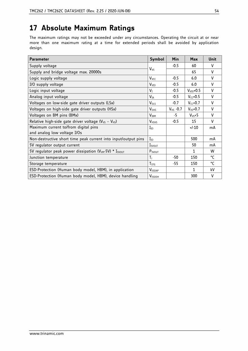
TMC262 / TMC262C DATASHEET (Rev. 2.25 / 2020-JUN-08) 54
www.trinamic.com
17 Absolute Maximum Ratings The maximum ratings may not be exceeded under any circumstances. Operating the circuit at or near more than one maximum rating at a time for extended periods shall be avoided by application design.
Parameter Symbol Min Max Unit
Supply voltage VVS
-0.5 60 V
Supply and bridge voltage max. 20000s 65 V
Logic supply voltage VVCC -0.5 6.0 V
I/O supply voltage VVIO -0.5 6.0 V
Logic input voltage VI -0.5 VVIO+0.5 V
Analog input voltage VIA -0.5 VCC+0.5 V
Voltages on low-side gate driver outputs (LSx) VOLS -0.7 VCC+0.7 V
Voltages on high-side gate driver outputs (HSx) VOHS VHS -0.7 VVS+0.7 V
Voltages on BM pins (BMx) VIBM -5 VVS+5 V
Relative high-side gate driver voltage (VVS – VHS) VHSVS -0.5 15 V
Maximum current to/from digital pins
and analog low voltage I/Os IIO +/-10 mA
Non-destructive short time peak current into input/output pins IIO 500 mA
5V regulator output current I5VOUT 50 mA
5V regulator peak power dissipation (VVM-5V) * I5VOUT P5VOUT 1 W
Junction temperature TJ -50 150 °C
Storage temperature TSTG -55 150 °C
ESD-Protection (Human body model, HBM), in application VESDAP 1 kV
ESD-Protection (Human body model, HBM), device handling VESDDH 300 V

TMC262 / TMC262C DATASHEET (Rev. 2.25 / 2020-JUN-08) 55
www.trinamic.com
18 Electrical Characteristics
18.1 Operational Range
Parameter Symbol Min Max Unit
Junction temperature TJ -40 125 °C
Supply voltage VVS 9 59 V
I/O supply voltage VVIO 3.00 5.25 V
18.2 DC and AC Specifications DC characteristics contain the spread of values guaranteed within the specified supply voltage range unless otherwise specified. Typical values represent the average value of all parts measured at +25°C. Temperature variation also causes some values to stray. A device with typical values will not leave Min/Max range within the full temperature range.
Power Supply Current DC Characteristics
VVS = 24.0V
Parameter Symbol Conditions Min Typ Max Unit
Supply current, operating IVS fCLK=16MHz, 40kHz chopper, QG=10nC
12 mA
Supply current, MOSFETs off IVS fCLK=16MHz, TMC262 10 mA
fCLK=16MHz, TMC262C 5 mA
Supply current, MOSFETs off, dependency on CLK frequency
IVS fCLK variable, TMC262
additional to IVS0
0.32 mA/
MHz
fCLK variable, TMC262C
additional to IVS0
0.1 mA/
MHz
Static supply current IVS0 fCLK=0Hz, digital inputs at +5V or GND
TMC262
3.2 4 mA
fCLK=0Hz, digital inputs at +5V or GND
TMC262C
3.5 5 mA
Part of supply current NOT consumed from 5V supply
IVSHV MOSFETs off 1.2 mA
IO supply current IVIO No load on outputs, inputs at VIO or GND
TMC262
0.3 µA
No load on outputs, inputs at VIO or GND
TMC262C
50 100 µA

TMC262 / TMC262C DATASHEET (Rev. 2.25 / 2020-JUN-08) 56
www.trinamic.com
NMOS Low-Side Driver DC Characteristics
VLSX = 2.5V, slope setting controlled by SLPL
Parameter Symbol Conditions Min Typ Max Unit
Gate drive current LSx low-side switch ON a)
ILSON SLPL=%00/%01 12 mA
Gate drive current LSx low-side switch ON a)
ILSON SLPL=%10 21 mA
Gate drive current LSx low-side switch ON a)
ILSON SLPL=%11, TMC262 20 31 50 mA
SLPL=%11, TMC262C 25 36 60 mA
Gate drive current LSx low-side switch OFF a)
ILSOFF SLPL=%00/%01 -13 mA
Gate drive current LSx low-side switch OFF a)
ILSOFF SLPL=%10 -25 mA
Gate drive current LSx low-side switch OFF a)
ILSOFF SLPL=%11, TMC262 -25 -37 -60 mA
SLPL=%11, TMC262C -35 -45 -70 mA
Gate off detector threshold VGOD VLSX falling 1 V
QGD protection resistance after detection of gate off
RLSOFFQGD SLPL=%11
VLSX = 1V
26 50
Driver active output voltage VLSON VVCC V
Notes:
a) Low-side drivers behave similar to a constant-current source between 0V and 2.5V (switching on) and between 2.5V and 5V (switching off), because switching MOSFETs go into saturation. At 2.5V, the output current is about 85% of peak value. This is the value specified.
PMOS High-Side Driver DC Characteristics
VVS = 24.0V, VVS - VHSX = 2.5V, slope setting controlled by SLPH
Parameter Symbol Conditions Min Typ Max Unit
Gate drive current HSx high-side switch ON b)
IHSON SLPH=%00/%01
-15 mA
Gate drive current HSx high-side switch ON b)
IHSON SLPH=%10 -29 mA
Gate drive current HSx high-side switch ON b)
IHSON SLPH=%11 -25 -42 -70 mA
Gate drive current HSx high-side switch OFF c)
IHSOFF SLPH=%00/%01 15 mA
Gate drive current HSx high-side switch OFF c)
IHSOFF SLPH=%10 29 mA
Gate drive current HSx high-side switch OFF c)
IHSOFF SLPH=%11 28 43 70 mA
Gate off detector threshold VGOD VHSX rising VVS-1 V
QGD protection resistance after detection of gate off
RHSOFFQGD SLPH=%11
VHSX = VVS - 1V
32 60
Driver active output voltage VHSON IOUT = 0mA, TMC262 VVHS+2.8 VVHS+2.3 VVHS+1.8 V
IOUT = 0mA, TMC262C VVHS-0 VVHS VVHS+0 V
Notes:
b) High-side switch on drivers behave similar to a constant-current source between VVS and VVS–2.5V. At VVS-2.5V, the output current is about 90% of peak value. This is the value specified.
c) High-side switch off drivers behave similar to a constant current source between VVS-8V and VVS-2.5V. At VVS-2.5V, the output current is about 65% of peak value. This is the value specified.

TMC262 / TMC262C DATASHEET (Rev. 2.25 / 2020-JUN-08) 57
www.trinamic.com
High-Side Voltage Regulator DC-Characteristics
VVS = 24.0V
Parameter Symbol Conditions Min Typ Max Unit
Output voltage (VVS – VHS) VHSVS IOUT = 0mA
TJ = 25°C
9.3 10.0 10.8 V
Output resistance RVHS Static load 50
Deviation of output voltage over the full temperature range
VVHS(DEV) TJ = full range 60 200 mV
DC Output current IVHS (from VS to VHS) 4 mA
Current limit IVHSMAX (from VS to VHS) 15 mA
Series regulator transistor output resistance (determines voltage drop at low supply
voltages)
RVHSLV 400 1000
Linear Regulator DC Characteristics
Parameter Symbol Conditions Min Typ Max Unit
Output voltage V5VOUT I5VOUT = 10mA
TJ = 25°C
4.75 5.0 5.25 V
Output resistance R5VOUT Static load 3
Deviation of output voltage over the full temperature range
V5VOUT(DEV) I5VOUT = 10mA
TJ = full range
30 60 mV
Output current capability
(attention, do not exceed maximum ratings with DC current)
I5VOUT VVS = 12V 100 mA
VVS = 8V 60 mA
VVS = 6.5V 20 mA
Clock Oscillator and CLK Input
Timing Characteristics
Parameter Symbol Conditions Min Typ Max Unit
Clock oscillator frequency fCLKOSC tJ=-50°C 10.0 14.3 MHz
Clock oscillator frequency fCLKOSC tJ=50°C 10.8 15.2 20.0 MHz
Clock oscillator frequency fCLKOSC tJ=150°C 15.4 20.3 MHz
External clock frequency (operating)
fCLK 4 20 MHz
External clock high / low level time
tCLK 12 ns
External clock high / low level time TMC262C
tCLK 15 ns
External clock transition time tTRCLK VINLO to VINHI or back 20 ns

TMC262 / TMC262C DATASHEET (Rev. 2.25 / 2020-JUN-08) 58
www.trinamic.com
Detector Levels DC Characteristics
Parameter Symbol Conditions Min Typ Max Unit
VVS undervoltage threshold VUV 6.5 8 8.5 V
Short to GND detector threshold
(VVS - VBMx)
VBMS2G 1.0 1.5 2.3 V
Short to GND detector threshold (sensitive setting)
(VVS - VBMx)
VBMS2G Option available for TMC262C, only
0.7 1.0 1.3 V
Short to GND detector delay (low-side gate off detected to short detection)
tS2G TS2G=00 2.0 3.2 4.5 µs
TS2G=10 1.6 µs
TS2G=01 1.2 µs
TS2G=11 0.8 µs
Overtemperature warning tOTPW 80 100 120 °C
Overtemperature shutdown tOT Temperature rising 135 150 170 °C
Overtemperature shutdown option
tOTLO Option available for TMC262C, only
136 °C
Sense Resistor Voltage Levels DC Characteristics
Parameter Symbol Conditions Min Typ Max Unit
Sense input peak threshold voltage (low sensitivity)
VSRTRIPL VSENSE=0, TMC262 Cx=248; Hyst.=0
290 310 330 mV
VSENSE=0, TMC262C Cx=248; Hyst.=0
310 323 340 mV
Sense input peak threshold voltage (high sensitivity)
VSRTRIPH VSENSE=1, TMC262 Cx=248; Hyst.=0
153 165 180 mV
VSENSE=1, TMC262C Cx=248; Hyst.=0
155 173 190 mV
Digital Logic Levels DC Characteristics
Parameter Symbol Conditions Min Typ Max Unit
Input voltage low level d) VINLO TMC262 -0.3 0.8 V
TMC262C -0.3 0.3 VVIO V
Input voltage high level d) VINHI TMC262 2.4 VVIO+0.3 V
TMC262C 0.7 VVIO VVIO+0.3 V
Output voltage low level VOUTLO IOUTLO = 1mA 0.4 V
Output voltage high level VOUTHI IOUTHI = -1mA 0.8VVIO V
Input leakage current IILEAK -10 10 µA
Notes:
d) Digital inputs left within or near the transition region substantially increase power supply current by drawing power from the internal 5V regulator. Make sure that digital inputs become driven near to 0V and up to the VIO I/O voltage. There are no on-chip pull-up or pull-down resistors on inputs.
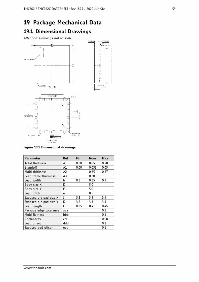
TMC262 / TMC262C DATASHEET (Rev. 2.25 / 2020-JUN-08) 59
www.trinamic.com
19 Package Mechanical Data
19.1 Dimensional Drawings Attention: Drawings not to scale.
Parameter Ref Min Nom Max
Total thickness A 0.80 0.85 0.90
Standoff A1 0.00 0.035 0.05
Mold thickness A2 - 0.65 0.67
Lead frame thickness A3 0.203
Lead width b 0.2 0.25 0.3
Body size X D 5.0
Body size Y E 5.0
Lead pitch e 0.5
Exposed die pad size X J 3.2 3.3 3.4
Exposed die pad size Y K 3.2 3.3 3.4
Lead length L 0.35 0.4 0.45
Package edge tolerance aaa 0.1
Mold flatness bbb 0.1
Coplanarity ccc 0.08
Lead offset ddd 0.1
Exposed pad offset eee 0.1
Figure 19.1 Dimensional drawings

TMC262 / TMC262C DATASHEET (Rev. 2.25 / 2020-JUN-08) 60
www.trinamic.com
19.2 Package Code
Device Package Temperature range Code/ Marking
TMC262 QFN32 (RoHS) -40° to +125°C Logo / TMC262-LA / YYWW
TMC262C QFN32 (RoHS) -40° to +125°C Logo / TMC262C-LA / WWYY
WW=Week, YY=Year Hint: Coding of date has been changed from TMC262 to TMC262C.
20 Disclaimer TRINAMIC Motion Control GmbH & Co. KG does not authorize or warrant any of its products for use in life support systems, without the specific written consent of TRINAMIC Motion Control GmbH & Co. KG. Life support systems are equipment intended to support or sustain life, and whose failure to perform, when properly used in accordance with instructions provided, can be reasonably expected to result in personal injury or death. Information given in this data sheet is believed to be accurate and reliable. However no responsibility is assumed for the consequences of its use nor for any infringement of patents or other rights of third parties which may result from its use. Specifications are subject to change without notice. All trademarks used are property of their respective owners.
21 ESD Sensitive Device The TMC262 is an ESD-sensitive CMOS device and sensitive to electrostatic discharge. Take special care to use adequate grounding of personnel and machines in manual handling. After soldering the devices to the board, ESD requirements are more relaxed. Failure to do so can result in defects or decreased reliability.
Note: In a modern SMD manufacturing process, ESD voltages well below 100V are standard. A major source for ESD is hot-plugging the motor during operation. As the power MOSFETs are discrete devices, the device in fact is very rugged concerning any ESD event on the motor outputs. All other connections are typically protected due to external circuitry on the PCB.
TMC262 / TMC262C DATASHEET (Rev. 2.25 / 2020-JUN-08) 61
www.trinamic.com
22 Table of Figures Figure 1.1 Applications block diagrams ......................................................................................................................... 4 Figure 2.1 TMC262 pin assignments ................................................................................................................................ 6 Figure 3.1 TMC262 block diagram .................................................................................................................................... 8 Figure 2 Standard application circuit .............................................................................................................................. 9 Figure 4.1 StallGuard2 load measurement SG as a function of load .................................................................. 10 Figure 4.2 Linear interpolation for optimizing SGT with changes in velocity .................................................. 12 Figure 5.1 Energy efficiency example with CoolStep ............................................................................................... 14 Figure 5.2 CoolStep adapts motor current to the load ........................................................................................... 15 Figure 6.1 SPI Timing ........................................................................................................................................................ 17 Figure 6.2 Interfaces to a TMC429 motion controller chip and a TMC262 motor driver ............................... 18 Figure 7.1 STEP/DIR timing .............................................................................................................................................. 29 Figure 7.2 Internal microstep table showing the first quarter of the sine wave ........................................... 30 Figure 7.3 MicroPlyer microstep interpolation with rising STEP frequency ...................................................... 31 Figure 8.1 Sense resistor grounding and protection components ...................................................................... 34 Figure 9.1 Chopper phases .............................................................................................................................................. 35 Figure 9.2 No ledges in current wave with sufficient hysteresis (magenta: current A, yellow & blue: sense resistor voltages A and B) ................................................................................................................................... 37 Figure 9.3 SpreadCycle chopper mode showing the coil current during a chopper cycle ........................... 37 Figure 9.4 Constant off-time chopper with offset showing the coil current during two cycles ................ 39 Figure 9.5 Zero crossing with correction using sine wave offset ........................................................................ 39 Figure 10.1 MOSFET gate charge vs. VDS for a typical MOSFET during a switching event ............................ 42 Figure 11.1 Short to GND detection timing ................................................................................................................ 43 Figure 11.2 Undervoltage reset timing ......................................................................................................................... 46 Figure 13.1 Start-up requirements of CLK input ........................................................................................................ 48 Figure 16.1 Schematic of TMC262-EVAL (power part) ............................................................................................... 52 Figure 16.2 Layout example ............................................................................................................................................. 53 Figure 19.1 Dimensional drawings ................................................................................................................................ 59

TMC262 / TMC262C DATASHEET (Rev. 2.25 / 2020-JUN-08) 62
www.trinamic.com
23 Revision History
Version Date Author BD = Bernhard Dwersteg
SD – Sonja Dwersteg
Description
1.00 2010-AUG-09 BD V2 silicon results, increased chopper thresholds (identical ratio of VCC power supply as in V1 and V1.2 silicon) VSENSE bit description corrected based on actual values
2.00 2012-FEB-03 SD Amended datasheet version for TMC262 (design and wording), Figure 5.1 new, Application examples on second front page new.
2.01 2012-FEB-20 SD Microstep resolution corrected (6.5.2).
2.02 2012-MAR-29 SD Description for CS parameter corrected (5) New table design for signal descriptions (2.2)
2.03 2012-JUN-07 SD Information about power supply sequencing added (12).
2.04 2012-AUG-01 SD Chapter 0: table layout corrected. Information about power supply sequencing updated.
2.05 2012-AUG-13 SD - Figure 11.2 (undervoltage reset timing) new
2.06 2012-NOV-05 SD Chapter 8 corrected: The low sensitivity (high sense resistor voltage, VSENSE=0) brings best and most robust current regulation, while high sensitivity (low sense resistor voltage; VSENSE=1) reduces power dissipation in the sense resistor.
2.08 2013-MAY-14 BD Updated MOSFET reference list Updated current ratings after tests / more coarse rating
2.09 2013-JUL-30 SD System clock information updated.
2.09a 2013-OKT-31 BD Updated MOSFET list and blue box, corrected table width for chapter 6.6
2.10 2013-NOV-29 BD Added hint not to leave CLK input floating (blue box), added external clock transition time parameter.
2.11 2014-MAY-12 SD Updated MOSFET list.
2.12 2015-JAN-13 BD Update to MOSFET list, rename some VM to VS, update chapter 16.3 and 16.1.
2.14 2016-JUL-14 BD Added figure for start-up requirements for CLK input
2.21 2.22
2018-NOV-16 2019-FEB-22
BD Added TMC262C device, Updated MOSFET list, added TMC262C electrical ratings, where different. Corrected error in TOFF calculation. Removed external gate driver example.
2.23 2020-JAN-15 BD Added marking for date coding, added thermal resistance
2.24 2020-MAR-10 BD Minor layout
2.25 2020-JUN-08 BD Updated Logo
24 References [TMC260] TMC260/261 Datasheet – TMC262 compatible driver with internal FETs for 40V, 2A [TMC261] TMC260/261 Datasheet – TMC262 compatible driver with internal FETs for 60V, 2A [TMC2660] TMC2660 Datasheet – TMC262 compatible driver with internal FETs for 30V, 4A [TMC262-EVAL] TMC262-EVAL Manual [AN-001] Application note for configuring SpreadCycle chopper Please refer to our web page http://www.trinamic.com.