TMC2225 Datasheet - Trinamic
75
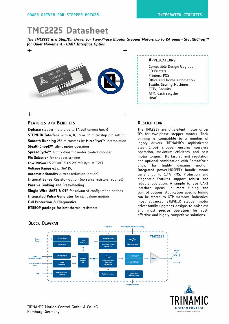
POWER DRIVER FOR STEPPER MOTORS INTEGRATED CIRCUITS TRINAMIC Motion Control GmbH & Co. KG Hamburg, Germany TMC2225 Datasheet APPLICATIONS Compatible Design Upgrade 3D Printers Printers, POS Office and home automation Textile, Sewing Machines CCTV, Security ATM, Cash recycler HVAC FEATURES AND BENEFITS 2-phase stepper motors up to 2A coil current (peak) STEP/DIR Interface with 4, 8, 16 or 32 microstep pin setting Smooth Running 256 microsteps by MicroPlyer™ interpolation StealthChop2™ silent motor operation SpreadCycle™ highly dynamic motor control chopper Pin Selection for chopper scheme Low RDSon LS 280mΩ & HS 290mΩ (typ. at 25°C) Voltage Range 4.75… 36V DC Automatic Standby current reduction (option) Internal Sense Resistor option (no sense resistors required) Passive Braking and Freewheeling Single Wire UART & OTP for advanced configuration options Integrated Pulse Generator for standalone motion Full Protection & Diagnostics HTSSOP package for best thermal resistance DESCRIPTION The TMC2225 are ultra-silent motor driver ICs for two-phase stepper motors. Their pinning is compatible to a number of legacy drivers. TRINAMICs sophisticated StealthChop2 chopper ensures noiseless operation, maximum efficiency and best motor torque. Its fast current regulation and optional combination with SpreadCycle allow for highly dynamic motion. Integrated power-MOSFETs handle motor current up to 1.4A RMS. Protection and diagnostic features support robust and reliable operation. A simple to use UART interface opens up more tuning and control options. Application specific tuning can be stored to OTP memory. Industries’ most advanced STEP/DIR stepper motor driver family upgrades designs to noiseless and most precise operation for cost- effective and highly competitive solutions. The TMC2225 is a Step/Dir Driver for Two-Phase Bipolar Stepper Motors up to 2A peak - StealthChop™ for Quiet Movement - UART Interface Option. BLOCK DIAGRAM
Transcript of TMC2225 Datasheet - Trinamic
POWER DRIVER FOR STEPPER MOTORS INTEGRATED CIRCUITS
TRINAMIC Motion Control GmbH & Co. KG Hamburg, Germany
TMC2225 Datasheet
APPLICATIONS
Compatible Design Upgrade 3D Printers Printers, POS Office and home automation Textile, Sewing Machines CCTV, Security ATM, Cash recycler HVAC
FEATURES AND BENEFITS
2-phase stepper motors up to 2A coil current (peak)
STEP/DIR Interface with 4, 8, 16 or 32 microstep pin setting
Smooth Running 256 microsteps by MicroPlyer™ interpolation
StealthChop2™ silent motor operation
SpreadCycle™ highly dynamic motor control chopper
Pin Selection for chopper scheme
Low RDSon LS 280mΩ & HS 290mΩ (typ. at 25°C)
Voltage Range 4.75… 36V DC
Automatic Standby current reduction (option)
Internal Sense Resistor option (no sense resistors required)
Passive Braking and Freewheeling
Single Wire UART & OTP for advanced configuration options
Integrated Pulse Generator for standalone motion
Full Protection & Diagnostics
HTSSOP package for best thermal resistance
DESCRIPTION
The TMC2225 are ultra-silent motor driver ICs for two-phase stepper motors. Their pinning is compatible to a number of legacy drivers. TRINAMICs sophisticated StealthChop2 chopper ensures noiseless operation, maximum efficiency and best motor torque. Its fast current regulation and optional combination with SpreadCycle allow for highly dynamic motion. Integrated power-MOSFETs handle motor current up to 1.4A RMS. Protection and diagnostic features support robust and reliable operation. A simple to use UART interface opens up more tuning and control options. Application specific tuning can be stored to OTP memory. Industries’ most advanced STEP/DIR stepper motor driver family upgrades designs to noiseless and most precise operation for cost-effective and highly competitive solutions.
The TMC2225 is a Step/Dir Driver for Two-Phase Bipolar Stepper Motors up to 2A peak - StealthChop™ for Quiet Movement - UART Interface Option.
BLOCK DIAGRAM

TMC2225 DATASHEET (Rev. 1.11 / 2020-JUN-02) 2
www.trinamic.com
APPLICATION EXAMPLES: SIMPLE SOLUTIONS – HIGHLY EFFECTIVE
The TMC2225 scores with power density, integrated power MOSFETs, smooth and quiet operation, and a congenial simplicity. The TMC2225 covers a wide spectrum of applications from battery systems to embedded applications with up to 2A motor current per coil. TRINAMICs unique chopper modes SpreadCycle and StealthChop2 optimize drive performance. StealthChop reduces motor noise to the point of silence at low velocities. Standby current reduction keeps costs for power dissipation and cooling down. Extensive support enables rapid design cycles and fast time-to-market with competitive products.
STANDALONE REPLACEMENT FOR LEGACY STEPPER DRIVER
S/D NS
0A+
0A-
0B+
TMC2225
0B-
ERROR, INDEX
S/D NS
0A+
0A-
0B+
TMC2225
0B-
UARTCPUHigh-Level Interface
UART INTERFACE FOR FULL DIAGNOSTICS AND CONTROL
Sense Resistors may be omitted
ORDER CODES
Order code PN Description Size [mm2]
TMC2225-SA 00-0174 StealthChop driver; HTSSOP28 (RoHS) 9.7 x 6.4
TMC2225-EVAL 40-0177 Evaluation board for TMC2225 stepper motor driver 85 x 55
ESELSBRÜCKE 40-0098 Connector board fitting to Landungsbrücke 61 x 38
LANDUNGSBRÜCKE 40-0167 Baseboard for TMC2225-EVAL and further evaluation boards
85 x 55
In this example, configuration is hard wired via pins. Software based motion control generates STEP and DIR (direction) signals, INDEX and ERROR signals report back status information.
A CPU operates the driver via step and direction signals. It accesses diagnostic information and configures the TMC2225 via the UART interface. The CPU manages motion control and the TMC2225 drives the motor and smoo-thens and optimizes drive performance.
The TMC2225-EVAL is part of TRINAMICs universal evaluation board system which provides a convenient handling of the hardware as well as a user-friendly software tool for evaluation. The TMC2225 evaluation board system consists of three parts: LANDUNGSBRÜCKE (base board), ESELSBRÜCKE (connector board with test points), and TMC2225-EVAL.

TMC2225 DATASHEET (Rev. 1.11 / 2020-JUN-02) 3
www.trinamic.com
Table of Contents
1 PRINCIPLES OF OPERATION ......................... 4
1.1 KEY CONCEPTS ................................................ 5 1.2 CONTROL INTERFACES ..................................... 6 1.3 MOVING AND CONTROLLING THE MOTOR ........ 6 1.4 STEALTHCHOP2 & SPREADCYCLE DRIVER ....... 6 1.5 PRECISE CLOCK GENERATOR AND CLK INPUT... 7 1.6 AUTOMATIC STANDSTILL POWER DOWN......... 7 1.7 INDEX OUTPUT ................................................ 7
2 PIN ASSIGNMENTS ........................................... 8
2.1 PACKAGE OUTLINE TMC2225 ........................ 8 2.2 SIGNAL DESCRIPTIONS TMC2225 .................. 8
3 SAMPLE CIRCUITS .......................................... 10
3.1 STANDARD APPLICATION CIRCUIT ................ 10 3.2 INTERNAL RDSON SENSING .......................... 10 3.3 5V ONLY SUPPLY .......................................... 11 3.4 CONFIGURATION PINS .................................. 12 3.5 HIGH MOTOR CURRENT ................................. 12 3.6 DRIVER PROTECTION AND EME CIRCUITRY ... 13
4 UART SINGLE WIRE INTERFACE ................ 14
4.1 DATAGRAM STRUCTURE ................................. 14 4.2 CRC CALCULATION ....................................... 16 4.3 UART SIGNALS ............................................ 16 4.4 ADDRESSING MULTIPLE SLAVES .................... 17
5 REGISTER MAP ................................................. 18
5.1 GENERAL REGISTERS ..................................... 19 5.2 VELOCITY DEPENDENT CONTROL ................... 24 5.3 SEQUENCER REGISTERS ................................. 25 5.4 CHOPPER CONTROL REGISTERS ..................... 26
6 STEALTHCHOP™ .............................................. 32
6.1 AUTOMATIC TUNING ..................................... 32 6.2 STEALTHCHOP OPTIONS ................................ 35 6.3 STEALTHCHOP CURRENT REGULATOR ............. 35 6.4 VELOCITY BASED SCALING ............................ 37 6.5 COMBINING STEALTHCHOP AND SPREADCYCLE . ..................................................................... 39 6.6 FLAGS IN STEALTHCHOP ............................... 40 6.7 FREEWHEELING AND PASSIVE BRAKING ........ 41
7 SPREADCYCLE CHOPPER ............................... 43
7.1 SPREADCYCLE SETTINGS ............................... 44
8 SELECTING SENSE RESISTORS .................... 47
9 MOTOR CURRENT CONTROL ........................ 48
9.1 ANALOG CURRENT SCALING VREF ............... 49
10 INTERNAL SENSE RESISTORS ..................... 51
11 STEP/DIR INTERFACE .................................... 53
11.1 TIMING ......................................................... 53 11.2 CHANGING RESOLUTION ............................... 54 11.3 MICROPLYER STEP INTERPOLATOR AND STAND
STILL DETECTION ....................................................... 55 11.4 INDEX OUTPUT ............................................. 56
12 INTERNAL STEP PULSE GENERATOR ......... 57
13 DRIVER DIAGNOSTIC FLAGS ...................... 58
13.1 TEMPERATURE MEASUREMENT ....................... 58 13.2 SHORT PROTECTION ...................................... 58 13.3 OPEN LOAD DIAGNOSTICS ........................... 59 13.4 DIAGNOSTIC OUTPUT ................................... 59
14 QUICK CONFIGURATION GUIDE ................ 60
15 EXTERNAL RESET ............................................. 63
16 CLOCK OSCILLATOR AND INPUT ............... 63
17 ABSOLUTE MAXIMUM RATINGS ................. 64
18 ELECTRICAL CHARACTERISTICS ................. 64
18.1 OPERATIONAL RANGE ................................... 64 18.2 DC AND TIMING CHARACTERISTICS .............. 65 18.3 THERMAL CHARACTERISTICS.......................... 69
19 LAYOUT CONSIDERATIONS ......................... 70
19.1 EXPOSED DIE PAD ........................................ 70 19.2 WIRING GND .............................................. 70 19.3 SUPPLY FILTERING ........................................ 70 19.4 LAYOUT EXAMPLE TMC2225 ........................ 71
20 PACKAGE MECHANICAL DATA .................... 72
20.1 DIMENSIONAL DRAWINGS HTSSOP28 ........ 72 20.2 PACKAGE CODES ........................................... 73
21 TABLE OF FIGURES ......................................... 74
22 REVISION HISTORY ....................................... 75
23 REFERENCES ...................................................... 75
TMC2225 DATASHEET (Rev. 1.11 / 2020-JUN-02) 4
www.trinamic.com
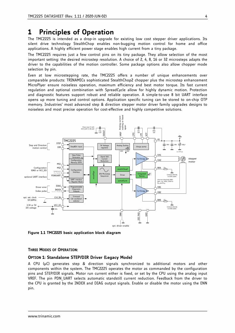
1 Principles of Operation The TMC2225 is intended as a drop-in upgrade for existing low cost stepper driver applications. Its silent drive technology StealthChop enables non-bugging motion control for home and office applications. A highly efficient power stage enables high current from a tiny package.
The TMC2225 requires just a few control pins on its tiny package. They allow selection of the most important setting: the desired microstep resolution. A choice of 2, 4, 8, 16 or 32 microsteps adapts the driver to the capabilities of the motion controller. Some package options also allow chopper mode selection by pin.
Even at low microstepping rate, the TMC2225 offers a number of unique enhancements over comparable products: TRINAMICs sophisticated StealthChop2 chopper plus the microstep enhancement MicroPlyer ensure noiseless operation, maximum efficiency and best motor torque. Its fast current regulation and optional combination with SpreadCycle allow for highly dynamic motion. Protection and diagnostic features support robust and reliable operation. A simple-to-use 8 bit UART interface opens up more tuning and control options. Application specific tuning can be stored to on-chip OTP memory. Industries’ most advanced step & direction stepper motor driver family upgrades designs to noiseless and most precise operation for cost-effective and highly competitive solutions.
22n50V
100n 16V
ENN
GND
DIE
PAD
mic
roPly
er
Full Bridge A
Full Bridge B
+VM
VS
steppermotor
NS
OA1
OA2
OB1
OB2
Driver
100n
BRB
100µF
CPI
CPO
BRA RSA
Use low inductivity SMD
type, e.g. 1206, 0.5W for
RSA and RSB
RSB
100nVCP
VREF
opt. driver enable
stealthChop2
spreadCycle
Integrated Rsense
IREF256 Microstep Sequencer
Stand Still Current
Reduction
2.2µ6.3V
5VOUT
Anal
og c
urren
t sc
alin
g o
r le
ave
open
Low ESR type
Place near IC with
short path to die pad
Connect directly
to GND plane
Connect directly
to GND plane
VCC_IO
TMC2225
Step&Dir input5V Voltage regulator
charge pump
CLK_INopt. ext. clock10-16MHz
3.3V or 5VI/O voltage
100n
Analog Scaling
VREF
Programmable Diagnostic Outputs
Configuration Interface
MS1
MS2
SPREAD
INDEX
DIAG
Configuration (GND or VCC_IO)
Index pulse
Driver error
PDN/UART B. Dwersteg, ©
TRINAMIC 2016
Trimmed CLK oscillator/
selector
UART interface + Register Block
Configuration Memory (OTP)
(not with TMC2202)
(only TMC222x)
optional UART interface
IREF
Step Pulse Generator
STEP
DIRStep and Direction
motion control
Figure 1.1 TMC2225 basic application block diagram
THREE MODES OF OPERATION:
OPTION 1: Standalone STEP/DIR Driver (Legacy Mode)
A CPU (µC) generates step & direction signals synchronized to additional motors and other components within the system. The TMC2225 operates the motor as commanded by the configuration pins and STEP/DIR signals. Motor run current either is fixed, or set by the CPU using the analog input VREF. The pin PDN_UART selects automatic standstill current reduction. Feedback from the driver to the CPU is granted by the INDEX and DIAG output signals. Enable or disable the motor using the ENN pin.

TMC2225 DATASHEET (Rev. 1.11 / 2020-JUN-02) 5
www.trinamic.com
OPTION 2: Standalone STEP/DIR Driver with OTP pre-configuration
Additional options enabled by pre-programming OTP memory (label UART & OTP):
+ Tuning of the chopper to the application for application tailored performance
+ Cost reduction by switching the driver to internal sense resistor mode
+ Adapting the automatic power down level and timing for best application efficiency
S/D NS
0A+
0A-
0B+
TMC2225
0B-
ERROR, INDEXCPUHigh-Level Interface
TXD only or bit bang UART
Other drivers External pre-programming
Figure 1.2 Stand-alone driver with pre-configuration
To enable the additional options, either one-time program the driver’s OTP memory, or store configuration in the CPU and transfer it to the on-chip registers following each power-up. Operation uses the same signals as Option 1. Programming does not need to be done within the application - it can be executed during testing of the PCB! Alternatively, use bit-banging by CPU firmware to configure the driver. Multiple drivers can be programmed at the same time using a single TXD line.
OPTION 3: STEP/DIR Driver with Full Diagnostics and Control
Similar to Option 2, but pin PDN_UART is connected to the CPU UART interface.
Additional options (label UART):
+ Detailed diagnostics and thermal management
+ Passive braking and freewheeling for flexible, lowest power stop modes
+ More options for microstep resolution setting (fullstep to 256 microstep)
+ Software controlled motor current setting and more chopper options
This mode allows replacing all control lines like ENN, DIAG, INDEX, MS1, MS2, and analog current setting VREF by a single interface line. This way, only three signals are required for full control: STEP, DIR and PDN_UART. Even motion without external STEP pulses is provided by an internal programmable step pulse generator: Just set the desired motor velocity. However, no ramping is provided by the TMC2225. Access to multiple driver ICs is possible using an analog multiplexer IC.
1.1 Key Concepts The TMC2225 implements advanced features which are exclusive to TRINAMIC products. These features contribute toward greater precision, greater energy efficiency, higher reliability, smoother motion, and cooler operation in many stepper motor applications. StealthChop2™ No-noise, high-precision chopper algorithm for inaudible motion and inaudible
standstill of the motor. Allows faster motor acceleration and deceleration than StealthChop™ and extends StealthChop to low stand still motor currents.
SpreadCycle™ High-precision cycle-by-cycle current control algorithm for highest dynamic movements.
MicroPlyer™ Microstep interpolator for obtaining full 256 microstep smoothness with lower
resolution step inputs starting from fullstep
In addition to these performance enhancements, TRINAMIC motor drivers offer safeguards to detect and protect against shorted outputs, output open-circuit, overtemperature, and undervoltage conditions for enhancing safety and recovery from equipment malfunctions.
UART
UART OTP

TMC2225 DATASHEET (Rev. 1.11 / 2020-JUN-02) 6
www.trinamic.com
1.2 Control Interfaces The TMC2225 supports both, discrete control lines for basic mode selection and a UART based single wire interface with CRC checking. The UART interface automatically becomes enabled when correct UART data is sent. When using UART, the pin selection may be disabled by control bits.
1.2.1 UART Interface The single wire interface allows unidirectional operation (for parameter setting only), or bi-directional operation for full control and diagnostics. It can be driven by any standard microcontroller UART or even by bit banging in software. Baud rates from 9600 Baud to 500k Baud or even higher (when using an external clock) may be used. No baud rate configuration is required, as the TMC2225 automatically adapts to the masters’ baud rate. The frame format is identical to the intelligent TRINAMIC controller & driver ICs TMC5130 and TMC5072. A CRC checksum allows data transmission over longer distance. For fixed initialization sequences, store the data including CRC into the µC, thus consuming only a few 100 bytes of code for a full initialization. CRC may be ignored during read access, if not desired. This makes CRC use an optional feature! The IC has a fixed address. Multiple drivers can be programmed in parallel by tying together all interface pins, in case no read access is required. An optional addressing can be provided by analog multiplexers, like 74HC4066.
From a software point of view the TMC2225 is a peripheral with a number of control and status registers. Most of them can either be written only or are read only. Some of the registers allow both, read and write access. In case read-modify-write access is desired for a write only register, a shadow register can be realized in master software.
1.3 Moving and Controlling the Motor
1.3.1 STEP/DIR Interface The motor is controlled by a step and direction input. Active edges on the STEP input can be rising edges or both rising and falling edges as controlled by a special mode bit (DEDGE). Using both edges cuts the toggle rate of the STEP signal in half, which is useful for communication over slow interfaces such as optically isolated interfaces. The state sampled from the DIR input upon an active STEP edge determines whether to step forward or back. Each step can be a fullstep or a microstep, in which there are 2, 4, 8, 16, 32, 64, 128, or 256 microsteps per fullstep. A step impulse with a low state on DIR increases the microstep counter and a high state decreases the counter by an amount controlled by the microstep resolution. An internal table translates the counter value into the sine and cosine values which control the motor current for microstepping.
1.3.2 Internal Step Pulse Generator Some applications do not require a precisely co-ordinate motion – the motor just is required to move for a certain time and at a certain velocity. The TMC2225 comes with an internal pulse generator for these applications: Just provide the velocity via UART interface to move the motor. The velocity sign automatically controls the direction of the motion. However, the pulse generator does not integrate a ramping function. Motion at higher velocities will require ramping up and ramping down the velocity value via software.
STEP/DIR mode and internal pulse generator mode can be mixed in an application!
1.4 StealthChop2 & SpreadCycle Driver StealthChop is a voltage chopper based principle. It especially guarantees that the motor is absolutely quiet in standstill and in slow motion, except for noise generated by ball bearings. Unlike other voltage mode choppers, StealthChop2 does not require any configuration. It automatically learns the best settings during the first motion after power up and further optimizes the settings in subsequent motions. An initial homing sequence is sufficient for learning. Optionally, initial learning parameters can be stored to OTP. StealthChop2 allows high motor dynamics, by reacting at once to a change of motor velocity.
UART
UART

TMC2225 DATASHEET (Rev. 1.11 / 2020-JUN-02) 7
www.trinamic.com
For highest velocity applications, SpreadCycle is an option to StealthChop2. It can be enabled via input pin (TMC222x) or via UART and OTP. StealthChop2 and SpreadCycle may even be used in a combined configuration for the best of both worlds: StealthChop2 for no-noise stand still, silent and smooth performance, SpreadCycle at higher velocity for high dynamics and highest peak velocity at low vibration.
SpreadCycle is an advanced cycle-by-cycle chopper mode. It offers smooth operation and good resonance dampening over a wide range of speed and load. The SpreadCycle chopper scheme automatically integrates and tunes fast decay cycles to guarantee smooth zero crossing performance.
Benefits of using StealthChop2:
- Significantly improved microstepping with low cost motors
- Motor runs smooth and quiet
- Absolutely no standby noise
- Reduced mechanical resonance yields improved torque
1.5 Precise clock generator and CLK input The TMC2225 provides a factory trimmed internal clock generator for precise chopper frequency and performance. However, an optional external clock input is available for cases, where quartz precision is desired, or where a lower or higher frequency is required. For safety, the clock input features timeout detection, and switches back to internal clock upon fail of the external source.
1.6 Automatic Standstill Power Down An automatic current reduction drastically reduces application power dissipation and cooling requirements. Per default, the stand still current reduction is enabled by pulling PDN_UART input to GND. It reduces standstill power dissipation to less than 33% by going to slightly more than half of the run current. Modify stand still current, delay time and decay via UART, or pre-programmed via internal OTP. Automatic freewheeling and passive motor braking are provided as an option for stand still. Passive braking reduces motor standstill power consumption to zero, while still providing effective dampening and braking!
t
CURRENT
TPOWERDOWNpower down delay timeRMS motor current trace with pin PDN=0
IHOLD
IRUN
IHOLDDELAYpower down ramp time
STEP
Figure 1.3 Automatic Motor Current Power Down
1.7 Index Output The index output gives one pulse per electrical rotation, i.e. one pulse per each four fullsteps. It shows the internal sequencer microstep 0 position (MSTEP near 0). This is the power on position. In combination with a mechanical home switch, a more precise homing is enabled.

TMC2225 DATASHEET (Rev. 1.11 / 2020-JUN-02) 8
www.trinamic.com
2 Pin Assignments The TMC2225 family comes in a thermally optimized HTSSOP package.
2.1 Package Outline TMC2225
MS2
INDEX
GND
CPO
VS
-
DIR
OB2
BRB
OA1
OB1
TEST
GND
5VOUT
VCC_IO
PDN_UART
DIAG
CPI
VCP
VS
BRA
OA2
ENN
STEP
CLK
MS1
SPREAD
VREF
12
34
56
7
21
20
19
18
17
16
15
TMC2225HTSSOP28
Pad=GND
© B. Dwersteg,
TRINAMIC
89
10
11
12
13
14
28
27
26
25
24
23
22
Figure 2.1 TMC2225 Pinning Top View – type: HTSSOP28, 9.7x6.4mm² over pins, 0.65mm pitch
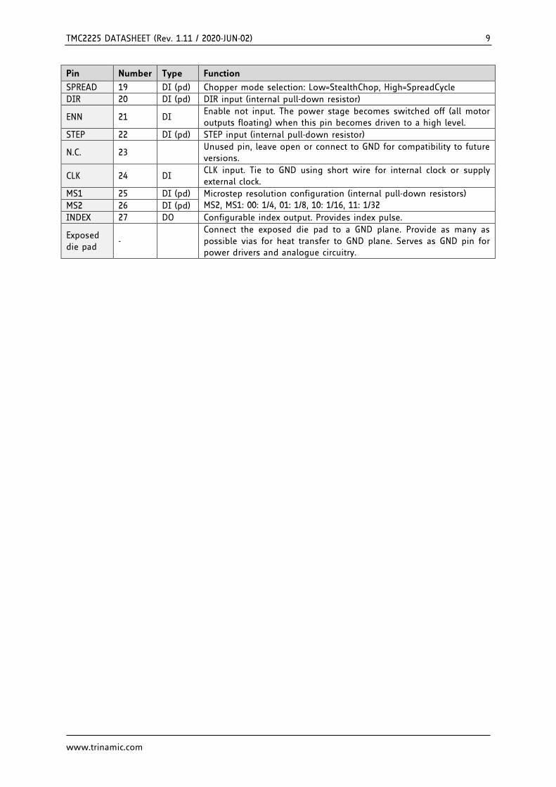
2.2 Signal Descriptions TMC2225 Pin Number Type Function
CPO 1 Charge pump capacitor output.
CPI 2 Charge pump capacitor input. Tie to CPO using 22nF 50V capacitor.
VCP 3 Charge pump voltage. Tie to VS using 100nF capacitor.
VS 4, 11 Motor supply voltage. Provide filtering capacity near pin with shortest possible loop to GND pad.
OA2 5 Motor coil A output 2
BRA 6 Sense resistor connection for coil A. Place sense resistor to GND near pin. Tie to GND when using internal sense resistor.
OA1 7 Motor coil A output 1
OB1 8 Motor coil B output 1
BRB 9 Sense resistor connection for coil B. Place sense resistor to GND near pin. Tie to GND when using internal sense resistor.
OB2 10 Motor coil B output 2
VREF 12 AI Analog reference voltage for current scaling or reference current for use of internal sense resistors (optional mode)
TEST 13 Connect to GND. May alternatively be left open or connected to VREF.
GND 14, 28 GND. Connect to GND plane near pin.
5VOUT 15 Output of internal 5V regulator. Attach 2.2µF to 4.7µF ceramic capacitor to GND near to pin for best performance. Provide the shortest possible loop to the GND pad.
VCC_IO 16 3.3V to 5V IO supply voltage for all digital pins.
PDN_UART 17 DIO (pd)
Power down not control input (low = automatic standstill current reduction). (internal pull-down resistor) Optional UART Input/Output. Power down function can be disabled in UART mode.
DIAG 18 DO Diagnostic output. Hi level upon driver error. Reset by ENN=high.
TMC2225 DATASHEET (Rev. 1.11 / 2020-JUN-02) 9
www.trinamic.com
Pin Number Type Function
SPREAD 19 DI (pd) Chopper mode selection: Low=StealthChop, High=SpreadCycle
DIR 20 DI (pd) DIR input (internal pull-down resistor)
ENN 21 DI Enable not input. The power stage becomes switched off (all motor outputs floating) when this pin becomes driven to a high level.
STEP 22 DI (pd) STEP input (internal pull-down resistor)
N.C. 23 Unused pin, leave open or connect to GND for compatibility to future versions.
CLK 24 DI CLK input. Tie to GND using short wire for internal clock or supply external clock.
MS1 25 DI (pd) Microstep resolution configuration (internal pull-down resistors) MS2, MS1: 00: 1/4, 01: 1/8, 10: 1/16, 11: 1/32 MS2 26 DI (pd)
INDEX 27 DO Configurable index output. Provides index pulse.
Exposed die pad
- Connect the exposed die pad to a GND plane. Provide as many as possible vias for heat transfer to GND plane. Serves as GND pin for power drivers and analogue circuitry.

TMC2225 DATASHEET (Rev. 1.11 / 2020-JUN-02) 10
www.trinamic.com
3 Sample Circuits The sample circuits show the connection of external components in different operation and supply modes. The connection of the bus interface and further digital signals is left out for clarity.
3.1 Standard Application Circuit
22n50V
100n 16V
ENN
GND
DIE
PAD
mic
roPly
er
Full Bridge A
Full Bridge B
+VM
VS
steppermotor
NS
OA1
OA2
OB1
OB2
Driver
100n
BRB
100µF
CPI
CPO
BRA RSA
Use low inductivity SMD
type, e.g. 1206, 0.5W for
RSA and RSB
RSB
100n
VCP
VREF
opt. driver enable
stealthChop2
spreadCycle
Integrated Rsense
IREF256 Microstep Sequencer
Stand Still Current
Reduction
2.2µ6.3V
5VOUT
Anal
og c
urren
t sc
alin
g o
r le
ave
open
Low ESR type
Place near IC with
short path to die pad
Connect directly
to GND plane
Connect directly
to GND plane
VCC_IO
TMC2225
Step&Dir input5V Voltage regulator
charge pump
CLK_INopt. ext. clock10-16MHz
3.3V or 5VI/O voltage
100n
Analog Scaling
VREF
Programmable Diagnostic Outputs
Configuration Interface
MS1
MS2
SPREAD
INDEX
DIAG
Configuration (GND or VCC_IO)
Index pulse
Driver error
PDN/UART B. Dwersteg, ©
TRINAMIC 2016
Trimmed CLK oscillator/
selector
UART interface + Register Block
Configuration Memory (OTP)
(not with TMC2202)
(only TMC222x)
optional UART interface
IREF
Step Pulse Generator
STEP
DIRStep and Direction
motion control
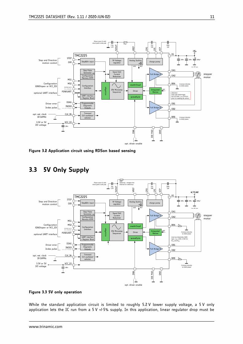
Figure 3.1 Standard application circuit
The standard application circuit uses a minimum set of additional components. Two sense resistors set the motor coil current. See chapter 8 to choose the right sense resistors. Use low ESR capacitors for filtering the power supply. The capacitors need to cope with the current ripple cause by chopper operation. A minimum capacity of 100µF near the driver is recommended for best performance. Current ripple in the supply capacitors also depends on the power supply internal resistance and cable length. VCC_IO can be supplied from 5VOUT, or from an external source, e.g. a 3.3V regulator.
Basic layout hints Place sense resistors and all filter capacitors as close as possible to the related IC pins. Use a solid common GND for all GND connections, also for sense resistor GND. Connect 5VOUT filtering capacitor directly to 5VOUT and the die pad. See layout hints for more details. Low ESR electrolytic capacitors are recommended for VS filtering.
3.2 Internal RDSon Sensing For cost critical or space limited applications, sense resistors can be omitted. For internal current sensing, a reference current set by a tiny external resistor programs the output current. For calculation of the reference resistor, refer chapter 9.1.
Attention Be sure to switch the IC to RDSon mode, before enabling drivers: Set otp_internalRsense = 1.
TMC2225 DATASHEET (Rev. 1.11 / 2020-JUN-02) 11
www.trinamic.com
VCC_IO
TMC2225
Step&Dir input5V Voltage regulator
charge pump
22n50V
100n 16V
CLK_IN
ENN
GND
DIE
PAD
opt. ext. clock10-16MHz
3.3V or 5VI/O voltage
100n
mic
roPly
er
Full Bridge A
Full Bridge B
+VM
VS
steppermotor
NS
OA1
OA2
OB1
OB2
Driver
100n
BRB
100µF
CPI
CPO
BRA
100n
VCP
Analog Scaling
VREF
VREF
opt. driver enable
Programmable Diagnostic Outputs
Configuration Interface
MS1
MS2
SPREAD
INDEX
DIAG
Configuration (GND/open or VCC_IO)
Index pulse
Driver error
PDN/UART B. Dwersteg, ©
TRINAMIC 2016
Trimmed CLK oscillator/
selector
UART interface + Register Block
Configuration Memory (OTP)
(not with TMC2202)
(only TMC222x)
stealthChop2
spreadCycle
Integrated Rsense
IREF
IREF256 Microstep Sequencer
Step Pulse Generator Stand Still
Current Reduction
STEP
DIR
2.2µ6.3V
5VOUT
Step and Direction motion control
RREF
Attention:
Start with ENN=high!
Set GCONF.1 or OTP0.6
prior to enabling the driver!
Low ESR type
Connect directly
to GND plane
Connect directly
to GND plane
Place near IC with
short path to die pad
optional UART interface
Figure 3.2 Application circuit using RDSon based sensing
3.3 5V Only Supply
22n50V
100n 16V
ENN
GND
DIE
PAD
mic
roPly
er
Full Bridge A
Full Bridge B
4.7-5.4V
VS
steppermotor
NS
OA1
OA2
OB1
OB2
Driver
100n
BRB
100µF
CPI
CPO
BRA RSA
RSB
100n
VCP
VREF
opt. driver enable
stealthChop2
spreadCycle
Integrated Rsense
IREF256 Microstep Sequencer
Stand Still Current
Reduction
10µ6.3V
5VOUT
10R
Use low inductivity SMD
type, e.g. 1206, 0.5W for
RSA and RSB
Low ESR type
Place near IC with
short path to die pad
Connect directly
to GND plane
Connect directly
to GND plane
VCC_IO
TMC2225
Step&Dir input5V Voltage regulator
charge pump
CLK_INopt. ext. clock10-16MHz
3.3V or 5VI/O voltage
100n
Analog Scaling
VREF
Programmable Diagnostic Outputs
Configuration Interface
MS1
MS2
SPREAD
INDEX
DIAG
Configuration (GND/open or VCC_IO)
Index pulse
Driver error
PDN/UART B. Dwersteg, ©
TRINAMIC 2016
Trimmed CLK oscillator/
selector
UART interface + Register Block
Configuration Memory (OTP)
(not with TMC2202)
(only TMC222x)
IREF
Step Pulse Generator
STEP
DIRStep and Direction
motion control
Optional – bridges the
internal 5V reference
optional UART interface
Figure 3.3 5V only operation
While the standard application circuit is limited to roughly 5.2 V lower supply voltage, a 5 V only application lets the IC run from a 5 V +/-5% supply. In this application, linear regulator drop must be

TMC2225 DATASHEET (Rev. 1.11 / 2020-JUN-02) 12
www.trinamic.com
minimized. Therefore, the internal 5V regulator is filtered with a higher capacitance. An optional resistor bridges the internal 5V regulator by connecting 5VOUT to the external power supply. This RC filter keeps chopper ripple away from 5VOUT. With this resistor, the external supply is the reference for the absolute motor current and must not exceed 5.5V.
3.4 Configuration Pins The TMC2225 family members provide three or four configuration pins depending on the package option. These pins allow quick configuration for standalone operation. Several additional options can be set by OTP programming. In UART mode, the configuration pins can be disabled in order to set a different configuration via registers.
PDN_UART: CONFIGURATION OF STANDSTILL POWER DOWN
PDN_UART Current Setting
GND Enable automatic power down in standstill periods
VCC_IO Disable
UART interface When using the UART interface, the configuration pin should be disabled via GCONF.pdn_disable = 1. Program IHOLD as desired for standstill periods.
SPREAD: SELECTION OF CHOPPER MODE
SPREAD Chopper Setting
GND or Pin open / not available
StealthChop is selected. Automatic switching to SpreadCycle in dependence of the step frequency can be programmed via OTP.
VCC_IO SpreadCycle operation.
MS1/MS2: CONFIGURATION OF MICROSTEP RESOLUTION FOR STEP INPUT
MS2 MS1 Microstep Setting
GND GND 4 microsteps (quarter step)
GND VCC_IO 8 microsteps
VCC_IO GND 16 microsteps
VCC_IO VCC_IO 32 microsteps
3.5 High Motor Current When operating at a high motor current, the driver power dissipation due to MOSFET switch on-resistance significantly heats up the driver. This power dissipation will significantly heat up the PCB cooling infrastructure, if operated at an increased duty cycle. This in turn leads to a further increase of driver temperature. An increase of temperature by about 100°C increases MOSFET resistance by roughly 50%. This is a typical behavior of MOSFET switches. Therefore, under high duty cycle, high load conditions, thermal characteristics have to be carefully taken into account, especially when increased environment temperatures are to be supported. Refer the thermal characteristics and the layout hints for more information. As a thumb rule, thermal properties of the PCB design become critical for the HTSSOP28 package at or above 1.2A RMS motor current for increased periods of time. Keep in mind that resistive power dissipation raises with the square of the motor current. On the other hand, this means that a small reduction of motor current significantly saves heat dissipation and energy.
Pay special attention to good thermal properties of your PCB layout, when going for 1.2A RMS current or more.
An effect which might be perceived at medium motor velocities and motor sine wave peak currents above roughly 1.4A peak is a slight sine distortion of the current wave when using SpreadCycle. It results from an increasing negative impact of parasitic internal diode conduction, which in turn
TMC2225 DATASHEET (Rev. 1.11 / 2020-JUN-02) 13
www.trinamic.com
negatively influences the duration of the fast decay cycle of the SpreadCycle chopper. This is, because the current measurement does not see the full coil current during this phase of the sine wave, because an increasing part of the current flows directly from the power MOSFETs’ drain to GND and does not flow through the sense resistor. This effect with most motors does not negatively influence the smoothness of operation, as it does not impact the critical current zero transition. The effect does not occur with StealthChop.
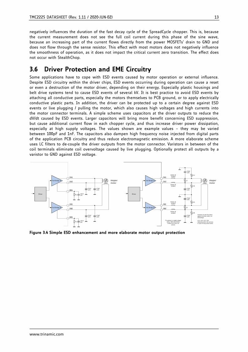
3.6 Driver Protection and EME Circuitry Some applications have to cope with ESD events caused by motor operation or external influence. Despite ESD circuitry within the driver chips, ESD events occurring during operation can cause a reset or even a destruction of the motor driver, depending on their energy. Especially plastic housings and belt drive systems tend to cause ESD events of several kV. It is best practice to avoid ESD events by attaching all conductive parts, especially the motors themselves to PCB ground, or to apply electrically conductive plastic parts. In addition, the driver can be protected up to a certain degree against ESD events or live plugging / pulling the motor, which also causes high voltages and high currents into the motor connector terminals. A simple scheme uses capacitors at the driver outputs to reduce the dV/dt caused by ESD events. Larger capacitors will bring more benefit concerning ESD suppression, but cause additional current flow in each chopper cycle, and thus increase driver power dissipation, especially at high supply voltages. The values shown are example values – they may be varied between 100pF and 1nF. The capacitors also dampen high frequency noise injected from digital parts of the application PCB circuitry and thus reduce electromagnetic emission. A more elaborate scheme uses LC filters to de-couple the driver outputs from the motor connector. Varistors in between of the coil terminals eliminate coil overvoltage caused by live plugging. Optionally protect all outputs by a varistor to GND against ESD voltage.
Full Bridge A
Full Bridge B
steppermotor
NS
OA1
OA2
OB1
OB2
Driver
470pF
100V
470pF
100V
470pF
100V
470pF
100V
Full Bridge A
Full Bridge B
steppermotor
NS
OA1
OA2
OB1
OB2
Driver
470pF
100V
470pF
100V
50Ohm @
100MHz
50Ohm @
100MHz
50Ohm @
100MHz
50Ohm @
100MHz
V1
V2
Fit varistors to supply voltage
rating. SMD inductivities
conduct full motor coil
current.
470pF
100V
470pF
100V
Varistors V1 and V2 protect
against inductive motor coil
overvoltage.
V1A, V1B, V2A, V2B:
Optional position for varistors
in case of heavy ESD events.
BRB
RSA
BRA
100nF
16V
RSB100nF
16V
V1A
V1B
V2A
V2B
Figure 3.4 Simple ESD enhancement and more elaborate motor output protection

TMC2225 DATASHEET (Rev. 1.11 / 2020-JUN-02) 14
www.trinamic.com
4 UART Single Wire Interface The UART single wire interface allows control of the TMC2225 with any microcontroller UART. It shares transmit and receive line like an RS485 based interface. Data transmission is secured using a cyclic redundancy check, so that increased interface distances (e.g. over cables between two PCBs) can be bridged without danger of wrong or missed commands even in the event of electro-magnetic disturbance. The automatic baud rate detection makes this interface easy to use.
4.1 Datagram Structure
4.1.1 Write Access
UART WRITE ACCESS DATAGRAM STRUCTURE
each byte is LSB…MSB, highest byte transmitted first
0 … 63
sync + reserved 8 bit slave address
RW + 7 bit register addr.
32 bit data CRC
0…7 8…15 16…23 24…55 56…63
1 0 1 0 Reserved (don’t cares but included in CRC)
SLAVEADDR=0 register address
1 data bytes 3, 2, 1, 0 (high to low byte)
CRC
0
1
2
3
4
5
6
7
8
…
15
16 …
23
24 …
55
56 …
63
A sync nibble precedes each transmission to and from the TMC2225 and is embedded into the first transmitted byte, followed by an addressing byte (0 for TMC2225). Each transmission allows a synchronization of the internal baud rate divider to the master clock. The actual baud rate is adapted and variations of the internal clock frequency are compensated. Thus, the baud rate can be freely chosen within the valid range. Each transmitted byte starts with a start bit (logic 0, low level on SWIOP) and ends with a stop bit (logic 1, high level on SWIOP). The bit time is calculated by measuring the time from the beginning of start bit (1 to 0 transition) to the end of the sync frame (1 to 0 transition from bit 2 to bit 3). All data is transmitted bytewise. The 32 bit data words are transmitted with the highest byte first. A minimum baud rate of 9000 baud is permissible, assuming 20 MHz clock (worst case for low baud rate). Maximum baud rate is fCLK/16 due to the required stability of the baud clock. The slave address SLAVEADDR is always 0 for the TMC2225. The communication becomes reset if a pause time of longer than 63 bit times between the start bits of two successive bytes occurs. This timing is based on the last correctly received datagram. In this case, the transmission needs to be restarted after a failure recovery time of minimum 12 bit times of bus idle time. This scheme allows the master to reset communication in case of transmission errors. Any pulse on an idle data line below 16 clock cycles will be treated as a glitch and leads to a timeout of 12 bit times, for which the data line must be idle. Other errors like wrong CRC are also treated the same way. This allows a safe re-synchronization of the transmission after any error conditions. Remark, that due to this mechanism an abrupt reduction of the baud rate to less than 15 percent of the previous value is not possible. Each accepted write datagram becomes acknowledged by the receiver by incrementing an internal cyclic datagram counter (8 bit). Reading out the datagram counter allows the master to check the success of an initialization sequence or single write accesses. Read accesses do not modify the counter.
UART
TMC2225 DATASHEET (Rev. 1.11 / 2020-JUN-02) 15
www.trinamic.com
The UART line must be logic high during idle state. Therefore, the power down function cannot be assigned by the pin PDN_UART in between of transmissions. In an application using the UART interface, set the desired power down function by register access and set pdn_disable in GCONF to disable the pin function.
4.1.2 Read Access
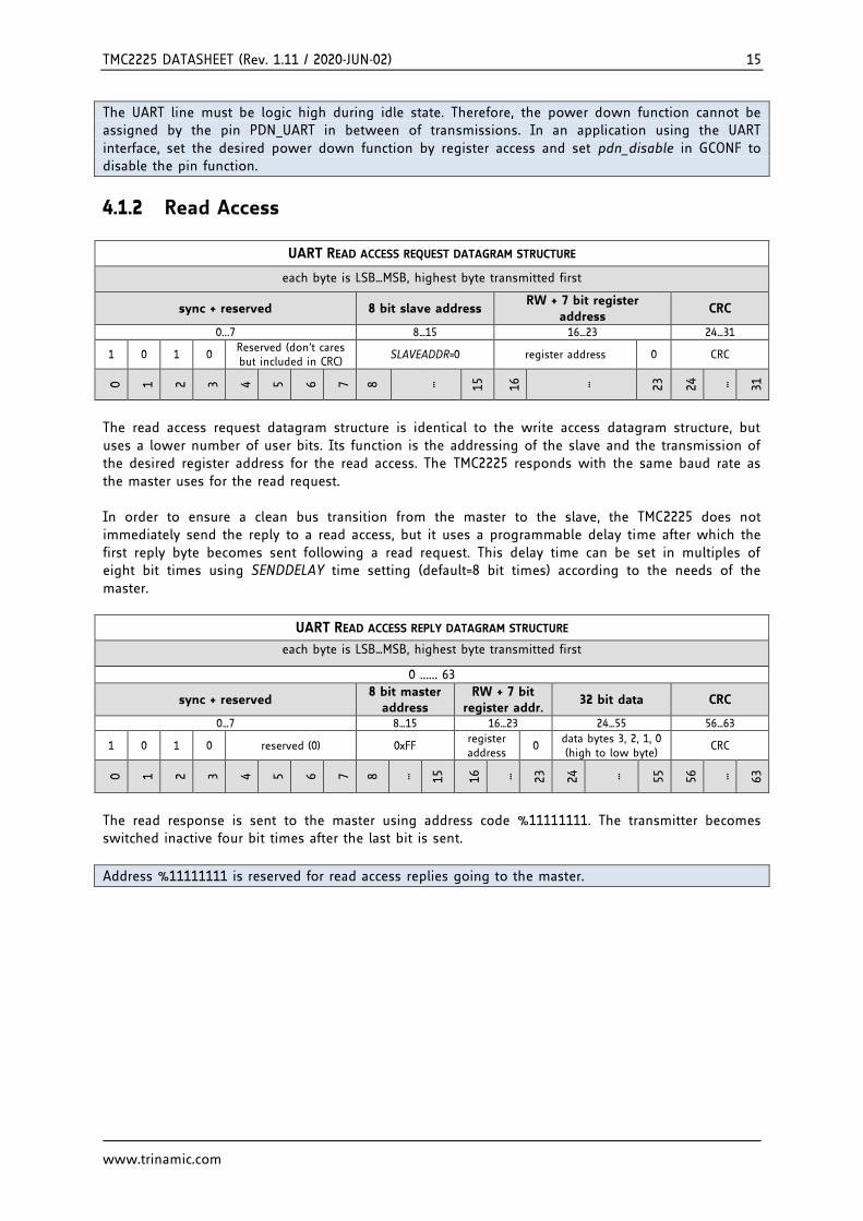
UART READ ACCESS REQUEST DATAGRAM STRUCTURE
each byte is LSB…MSB, highest byte transmitted first
sync + reserved 8 bit slave address RW + 7 bit register
address CRC
0...7 8…15 16…23 24…31
1 0 1 0 Reserved (don’t cares but included in CRC)
SLAVEADDR=0 register address 0 CRC
0
1
2
3
4
5
6
7
8
…
15
16 …
23
24 …
31
The read access request datagram structure is identical to the write access datagram structure, but uses a lower number of user bits. Its function is the addressing of the slave and the transmission of the desired register address for the read access. The TMC2225 responds with the same baud rate as the master uses for the read request. In order to ensure a clean bus transition from the master to the slave, the TMC2225 does not immediately send the reply to a read access, but it uses a programmable delay time after which the first reply byte becomes sent following a read request. This delay time can be set in multiples of eight bit times using SENDDELAY time setting (default=8 bit times) according to the needs of the master.
UART READ ACCESS REPLY DATAGRAM STRUCTURE
each byte is LSB…MSB, highest byte transmitted first
0 ...... 63
sync + reserved 8 bit master
address RW + 7 bit
register addr. 32 bit data CRC
0…7 8…15 16…23 24…55 56…63
1 0 1 0 reserved (0) 0xFF register address
0 data bytes 3, 2, 1, 0 (high to low byte)
CRC
0
1
2
3
4
5
6
7
8
…
15
16 …
23
24 …
55
56 …
63
The read response is sent to the master using address code %11111111. The transmitter becomes switched inactive four bit times after the last bit is sent.
Address %11111111 is reserved for read access replies going to the master.
TMC2225 DATASHEET (Rev. 1.11 / 2020-JUN-02) 16
www.trinamic.com
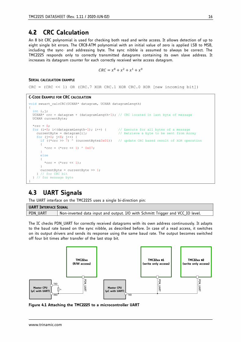
4.2 CRC Calculation An 8 bit CRC polynomial is used for checking both read and write access. It allows detection of up to eight single bit errors. The CRC8-ATM polynomial with an initial value of zero is applied LSB to MSB, including the sync- and addressing byte. The sync nibble is assumed to always be correct. The TMC2225 responds only to correctly transmitted datagrams containing its own slave address. It increases its datagram counter for each correctly received write access datagram.
𝐶𝑅𝐶 = 𝑥8 + 𝑥2 + 𝑥1 + 𝑥0 SERIAL CALCULATION EXAMPLE
CRC = (CRC << 1) OR (CRC.7 XOR CRC.1 XOR CRC.0 XOR [new incoming bit])
C-CODE EXAMPLE FOR CRC CALCULATION
void swuart_calcCRC(UCHAR* datagram, UCHAR datagramLength)
int i,j;
UCHAR* crc = datagram + (datagramLength-1); // CRC located in last byte of message
UCHAR currentByte;
*crc = 0;
for (i=0; i<(datagramLength-1); i++) // Execute for all bytes of a message
currentByte = datagram[i]; // Retrieve a byte to be sent from Array
for (j=0; j<8; j++)
if ((*crc >> 7) ^ (currentByte&0x01)) // update CRC based result of XOR operation
*crc = (*crc << 1) ^ 0x07;
else
*crc = (*crc << 1);
currentByte = currentByte >> 1;
// for CRC bit
// for message byte
4.3 UART Signals The UART interface on the TMC2225 uses a single bi-direction pin:
UART INTERFACE SIGNAL
PDN_UART Non-inverted data input and output. I/O with Schmitt Trigger and VCC_IO level.
The IC checks PDN_UART for correctly received datagrams with its own address continuously. It adapts to the baud rate based on the sync nibble, as described before. In case of a read access, it switches on its output drivers and sends its response using the same baud rate. The output becomes switched off four bit times after transfer of the last stop bit.
Master CPU (µC with UART)
TMC22xx(R/W access)
PDN_U
ART
TXD
RXD
1kMaster CPU
(µC with UART)
TMC22xx #1(write only access)
PDN_U
ART
TXD
TMC22xx #2(write only access)
PDN_U
ART
Figure 4.1 Attaching the TMC2225 to a microcontroller UART

TMC2225 DATASHEET (Rev. 1.11 / 2020-JUN-02) 17
www.trinamic.com
4.4 Addressing Multiple Slaves WRITE ONLY ACCESS
If read access is not used, and all slaves are to be programmed with the same initialization values, no addressing is required. All slaves can be programmed in parallel like a single device (Figure 4.1.).
ADDRESSING MULTIPLE SLAVES
As the TMC2225 uses a fixed UART address, in principle only one IC can be accessed per UART interface channel. Adding analog switches allows separated access to individual ICs. This scheme is similar to an SPI bus with individual slave select lines (Figure 4.2).
Master CPU (µC with UART)
TMC22xx#1
PDN_U
ART
TMC22xx#2
TMC22xx#3
TXD
RXD
+VIO
1k
22k
SW
O ¼ 74HC4066Select#1Port pin
Port pin
Port pin
PDN_U
ART
+VIO
22kS
WO ¼ 74HC4066
PDN_U
ART
+VIO
22k
SW
O ¼ 74HC4066
Select#2
Select#3
74HC1G125
Optional buffer for transmission over long lines or many slaves.
Port pin
Figure 4.2 Addressing multiple TMC2225 via single wire interface using analog switches
PROCEED AS FOLLOWS TO CONTROL MULTIPLE SLAVES:
- Set the UART to 8 bits, no parity. Select a baud rate safely within the valid range. At 250kBaud, a write access transmission requires 320µs (=8 Bytes * (8+2) bits * 4µs).
- Before starting an access, activate the select pin going to the analog switch by setting it high. All other slaves select lines shall be off, unless a broadcast is desired.
- When using the optional buffer, set TMC2225 transmission send delay to an appropriate value allowing the µC to switch off the buffer before receiving reply data.
- To start a transmission, activate the TXD line buffer by setting the control pin low. - When sending a read access request, switch off the buffer after transmission of the last stop
bit is finished. - Take into account, that all transmitted data also is received by the RXD input.

TMC2225 DATASHEET (Rev. 1.11 / 2020-JUN-02) 18
www.trinamic.com
5 Register Map This chapter gives an overview of the complete register set. Some of the registers bundling a number of single bits are detailed in extra tables. The functional practical application of the settings is detailed in dedicated chapters.
Note - Reset default: All registers become reset to 0 upon power up, unless otherwise noted. - Add 0x80 to the address Addr for write accesses!
NOTATION OF HEXADECIMAL AND BINARY NUMBERS
0x precedes a hexadecimal number, e.g. 0x04
% precedes a multi-bit binary number, e.g. %100
NOTATION OF R/W FIELD
R Read only
W Write only
R/W Read- and writable register
R+C Clear upon read
OVERVIEW REGISTER MAPPING
REGISTER DESCRIPTION
General Configuration Registers These registers contain
- global configuration
- global status flags
- OTP read access and programming
- interface configuration
Velocity Dependent Driver Feature Control Register Set
This register set offers registers for
- driver current control, stand still reduction
- setting thresholds for different chopper modes
- internal pulse generator control
Chopper Register Set This register set offers registers for
- optimization of StealthChop2 and SpreadCycle and read out of internal values
- passive braking and freewheeling options
- driver diagnostics
- driver enable / disable
UART

TMC2225 DATASHEET (Rev. 1.11 / 2020-JUN-02) 19
www.trinamic.com
5.1 General Registers
GENERAL CONFIGURATION REGISTERS (0X00…0X0F)
R/W Addr n Register Description / bit names
RW 0x00 10 GCONF
Bit GCONF – Global configuration flags
0 I_scale_analog (Reset default=1) 0: Use internal reference derived from 5VOUT 1: Use voltage supplied to VREF as current reference
1 internal_Rsense (Reset default: OTP) 0: Operation with external sense resistors 1: Internal sense resistors. Use current supplied into
VREF as reference for internal sense resistor. VREF pin internally is driven to GND in this mode.
2 en_SpreadCycle (Reset default: OTP) 0: StealthChop PWM mode enabled (depending on
velocity thresholds). Initially switch from off to on state while in stand still, only.
1: SpreadCycle mode enabled A high level on the pin SPREAD (TMC222x, only) inverts this flag to switch between both chopper modes.
3 shaft 1: Inverse motor direction
4 index_otpw 0: INDEX shows the first microstep position of
sequencer 1: INDEX pin outputs overtemperature prewarning
flag (otpw) instead
5 index_step 0: INDEX output as selected by index_otpw 1: INDEX output shows step pulses from internal
pulse generator (toggle upon each step)
6 pdn_disable 0: PDN_UART controls standstill current reduction 1: PDN_UART input function disabled. Set this bit,
when using the UART interface!
7 mstep_reg_select 0: Microstep resolution selected by pins MS1, MS2 1: Microstep resolution selected by MSTEP register
8 multistep_filt (Reset default=1) 0: No filtering of STEP pulses 1: Software pulse generator optimization enabled
when fullstep frequency > 750Hz (roughly). TSTEP shows filtered step time values when active.
9 test_mode 0: Normal operation 1: Enable analog test output on pin ENN (pull-down
resistor off), ENN treated as enabled. IHOLD[1..0] selects the function of DCO:
0…2: T120, DAC, VDDH Attention: Not for user, set to 0 for normal operation!

TMC2225 DATASHEET (Rev. 1.11 / 2020-JUN-02) 20
www.trinamic.com
GENERAL CONFIGURATION REGISTERS (0X00…0X0F)
R/W Addr n Register Description / bit names
R+ WC
0x01 3 GSTAT
Bit GSTAT – Global status flags (Re-Write with ‘1’ bit to clear respective flags)
0 reset 1: Indicates that the IC has been reset since the last
read access to GSTAT. All registers have been cleared to reset values.
1 drv_err 1: Indicates, that the driver has been shut down
due to overtemperature or short circuit detection since the last read access. Read DRV_STATUS for details. The flag can only be cleared when all error conditions are cleared.
2 uv_cp 1: Indicates an undervoltage on the charge pump.
The driver is disabled in this case. This flag is not latched and thus does not need to be cleared.
R 0x02 8 IFCNT
Interface transmission counter. This register becomes incremented with each successful UART interface write access. Read out to check the serial transmission for lost data. Read accesses do not change the content. The counter wraps around from 255 to 0.
W 0x03 4 SLAVECONF
Bit SLAVECONF
11..8 SENDDELAY for read access (time until reply is sent): 0, 1: 8 bit times 2, 3: 3*8 bit times 4, 5: 5*8 bit times 6, 7: 7*8 bit times 8, 9: 9*8 bit times 10, 11: 11*8 bit times 12, 13: 13*8 bit times 14, 15: 15*8 bit times
W 0x04 16 OTP_PROG
Bit OTP_PROGRAM – OTP programming Write access programs OTP memory (one bit at a time), Read access refreshes read data from OTP after a write
2..0 OTPBIT Selection of OTP bit to be programmed to the selected byte location (n=0..7: programs bit n to a logic 1)
5..4
OTPBYTE Selection of OTP programming location (0, 1 or 2)
15..8 OTPMAGIC Set to 0xbd to enable programming. A programming time of minimum 10ms per bit is recommended (check by reading OTP_READ).
R 0x05 24 OTP_READ
Bit OTP_READ (Access to OTP memory result and update) See separate table!
7..0 OTP0 byte 0 read data
15..8 OTP1 byte 1 read data
23..16 OTP2 byte 2 read data
R 0x06 10 + 8
IOIN
Bit INPUT (Reads the state of all input pins available)
0 ENN (TMC220x)
1 PDN_UART (TMC222x)
2 MS1 (TMC220x), SPREAD (TMC222x)
3 MS2 (TMC220x), DIR (TMC222x)
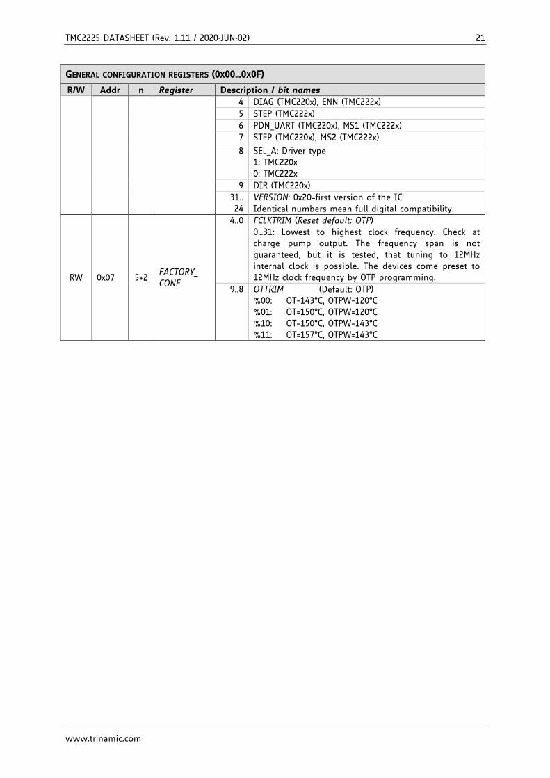
TMC2225 DATASHEET (Rev. 1.11 / 2020-JUN-02) 21
www.trinamic.com
GENERAL CONFIGURATION REGISTERS (0X00…0X0F)
R/W Addr n Register Description / bit names
4 DIAG (TMC220x), ENN (TMC222x)
5 STEP (TMC222x)
6 PDN_UART (TMC220x), MS1 (TMC222x)
7 STEP (TMC220x), MS2 (TMC222x)
8 SEL_A: Driver type 1: TMC220x 0: TMC222x
9 DIR (TMC220x)
31.. 24
VERSION: 0x20=first version of the IC Identical numbers mean full digital compatibility.
RW 0x07 5+2 FACTORY_ CONF
4..0 FCLKTRIM (Reset default: OTP) 0…31: Lowest to highest clock frequency. Check at charge pump output. The frequency span is not guaranteed, but it is tested, that tuning to 12MHz internal clock is possible. The devices come preset to 12MHz clock frequency by OTP programming.
9..8 OTTRIM (Default: OTP) %00: OT=143°C, OTPW=120°C %01: OT=150°C, OTPW=120°C %10: OT=150°C, OTPW=143°C %11: OT=157°C, OTPW=143°C

TMC2225 DATASHEET (Rev. 1.11 / 2020-JUN-02) 22
www.trinamic.com
5.1.1 OTP_READ – OTP configuration memory The OTP memory holds power up defaults for certain registers. All OTP memory bits are cleared to 0 by default. Programming only can set bits, clearing bits is not possible. Factory tuning of the clock frequency affects otp0.0 to otp0.4. The state of these bits therefore may differ between individual ICs.
0X05: OTP_READ – OTP MEMORY MAP
Bit Name Function Comment
23 otp2.7 otp_en_SpreadCycle This flag determines if the driver defaults to SpreadCycle or to StealthChop.
0 Default: StealthChop (GCONF.en_SpreadCycle=0) OTP 1.0 to 1.7 and 2.0 used for StealthChop SpreadCycle settings: HEND=0; HSTART=5; TOFF=3
1
Default: SpreadCycle (GCONF.en_SpreadCycle=1) OTP 1.0 to 1.7 and 2.0 used for SpreadCycle StealthChop settings: PWM_GRAD=0; TPWM_THRS=0; PWM_OFS=36; pwm_autograd=1
22 otp2.6 OTP_IHOLD Reset default for standstill current IHOLD (used only if current reduction enabled, e.g. pin PDN_UART low). %00: IHOLD= 16 (53% of IRUN) %01: IHOLD= 2 ( 9% of IRUN) %10: IHOLD= 8 (28% of IRUN) %11: IHOLD= 24 (78% of IRUN) (Reset default for run current IRUN=31)
21 otp2.5
20 otp2.4 OTP_IHOLDDELAY Reset default for IHOLDDELAY %00: IHOLDDELAY= 1 %01: IHOLDDELAY= 2 %10: IHOLDDELAY= 4 %11: IHOLDDELAY= 8
19 otp2.3
18 otp2.2 otp_PWM_FREQ Reset default for PWM_FREQ: 0: PWM_FREQ=%01=2/683 1: PWM_FREQ=%10=2/512
17 otp2.1 otp_PWM_REG Reset default for PWM_REG: 0: PWM_REG=%1000: max. 4 increments / cycle 1: PWM_REG=%0010: max. 1 increment / cycle
16 otp2.0 otp_PWM_OFS
Depending on otp_en_SpreadCycle
0 0: PWM_OFS=36 1: PWM_OFS=00 (no feed forward scaling); pwm_autograd=0
OTP_CHOPCONF8 1 Reset default for CHOPCONF.8 (hend1)
15 otp1.7 OTP_TPWMTHRS
Depending on otp_en_SpreadCycle
14 otp1.6 0 Reset default for TPWM_THRS as defined by (0..7): 0: TPWM_THRS= 0 1: TPWM_THRS= 200 2: TPWM_THRS= 300 3: TPWM_THRS= 400 4: TPWM_THRS= 500 5: TPWM_THRS= 800 6: TPWM_THRS= 1200 7: TPWM_THRS= 4000
13 otp1.5
OTP_CHOPCONF7...5 1 Reset default for CHOPCONF.5 to CHOPCONF.7 (hstrt1, hstrt2 and hend0)
12 otp1.4 otp_pwm_autograd
Depending on otp_en_SpreadCycle
0 0: pwm_autograd=1 1: pwm_autograd=0
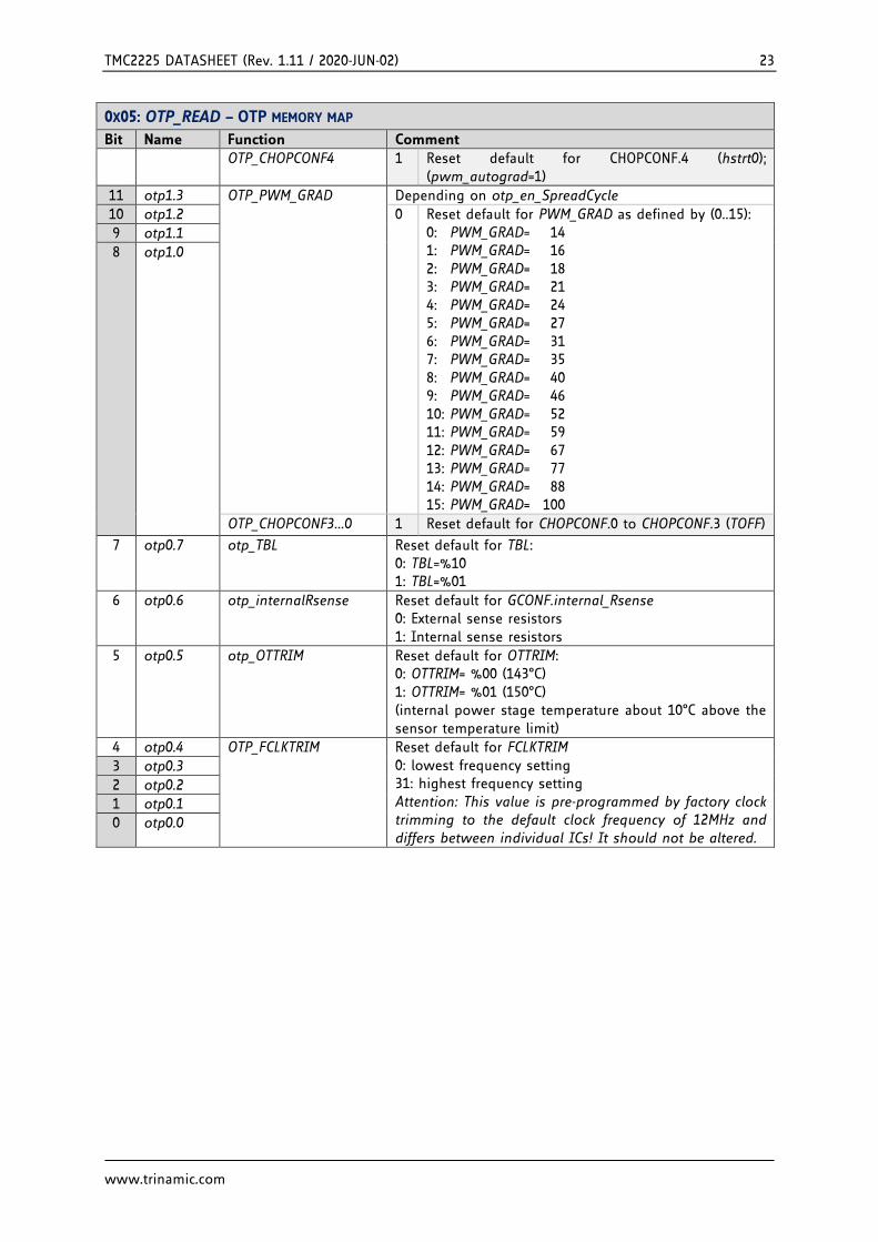
TMC2225 DATASHEET (Rev. 1.11 / 2020-JUN-02) 23
www.trinamic.com
0X05: OTP_READ – OTP MEMORY MAP
Bit Name Function Comment
OTP_CHOPCONF4 1 Reset default for CHOPCONF.4 (hstrt0); (pwm_autograd=1)
11 otp1.3 OTP_PWM_GRAD
Depending on otp_en_SpreadCycle
10 otp1.2 0
Reset default for PWM_GRAD as defined by (0..15): 0: PWM_GRAD= 14 1: PWM_GRAD= 16 2: PWM_GRAD= 18 3: PWM_GRAD= 21 4: PWM_GRAD= 24 5: PWM_GRAD= 27 6: PWM_GRAD= 31 7: PWM_GRAD= 35 8: PWM_GRAD= 40 9: PWM_GRAD= 46 10: PWM_GRAD= 52 11: PWM_GRAD= 59 12: PWM_GRAD= 67 13: PWM_GRAD= 77 14: PWM_GRAD= 88 15: PWM_GRAD= 100
9 otp1.1
8 otp1.0
OTP_CHOPCONF3...0 1 Reset default for CHOPCONF.0 to CHOPCONF.3 (TOFF)
7 otp0.7 otp_TBL Reset default for TBL: 0: TBL=%10 1: TBL=%01
6 otp0.6 otp_internalRsense Reset default for GCONF.internal_Rsense 0: External sense resistors 1: Internal sense resistors
5 otp0.5 otp_OTTRIM Reset default for OTTRIM: 0: OTTRIM= %00 (143°C) 1: OTTRIM= %01 (150°C) (internal power stage temperature about 10°C above the sensor temperature limit)
4 otp0.4 OTP_FCLKTRIM Reset default for FCLKTRIM 0: lowest frequency setting 31: highest frequency setting Attention: This value is pre-programmed by factory clock trimming to the default clock frequency of 12MHz and differs between individual ICs! It should not be altered.
3 otp0.3
2 otp0.2
1 otp0.1
0 otp0.0

TMC2225 DATASHEET (Rev. 1.11 / 2020-JUN-02) 24
www.trinamic.com
5.2 Velocity Dependent Control
VELOCITY DEPENDENT DRIVER FEATURE CONTROL REGISTER SET (0X10…0X1F)
R/W Addr n Register Description / bit names
W 0x10
5 + 5 + 4
IHOLD_IRUN
Bit IHOLD_IRUN – Driver current control
4..0 IHOLD (Reset default: OTP) Standstill current (0=1/32 … 31=32/32) In combination with StealthChop mode, setting IHOLD=0 allows to choose freewheeling or coil short circuit (passive braking) for motor stand still.
12..8 IRUN (Reset default=31) Motor run current (0=1/32 … 31=32/32) Hint: Choose sense resistors in a way, that normal IRUN is 16 to 31 for best microstep performance.
19..16 IHOLDDELAY (Reset default: OTP) Controls the number of clock cycles for motor power down after standstill is detected (stst=1) and TPOWERDOWN has expired. The smooth transition avoids a motor jerk upon power down. 0: instant power down 1..15: Delay per current reduction step in multiple
of 2^18 clocks
W 0x11 8 TPOWER DOWN
TPOWERDOWN (Reset default=20) Sets the delay time from stand still (stst) detection to motor current power down. Time range is about 0 to 5.6 seconds. 0…((2^8)-1) * 2^18 tCLK
Attention: A minimum setting of 2 is required to allow automatic tuning of StealthChop PWM_OFFS_AUTO.
R 0x12 20 TSTEP
Actual measured time between two 1/256 microsteps derived from the step input frequency in units of 1/fCLK. Measured value is (2^20)-1 in case of overflow or stand still. The TSTEP related threshold uses a hysteresis of 1/16 of the compare value to compensate for jitter in the clock or the step frequency: (Txxx*15/16)-1 is the lower compare value for each TSTEP based comparison. This means, that the lower switching velocity equals the calculated setting, but the upper switching velocity is higher as defined by the hysteresis setting.
W 0x13 20 TPWMTHRS
Sets the upper velocity for StealthChop voltage PWM mode. TSTEP ≥ TPWMTHRS
- StealthChop PWM mode is enabled, if configured When the velocity exceeds the limit set by TPWMTHRS, the driver switches to SpreadCycle. 0: Disabled
W 0x22 24 VACTUAL
VACTUAL allows moving the motor by UART control. It gives the motor velocity in +-(2^23)-1 [µsteps / t] 0: Normal operation. Driver reacts to STEP input. /=0: Motor moves with the velocity given by VACTUAL. Step pulses can be monitored via INDEX output. The motor direction is controlled by the sign of VACTUAL.

TMC2225 DATASHEET (Rev. 1.11 / 2020-JUN-02) 25
www.trinamic.com
5.3 Sequencer Registers The sequencer registers have a pure informative character and are read-only. They help for special cases like storing the last motor position before power off in battery powered applications.
MICROSTEPPING CONTROL REGISTER SET (0X60…0X6B)
R/W Addr n Register Description / bit names Range [Unit]
R 0x6A 10 MSCNT
Microstep counter. Indicates actual position in the microstep table for CUR_A. CUR_B uses an offset of 256 into the table. Reading out MSCNT allows determination of the motor position within the electrical wave.
0…1023
R 0x6B 9 + 9
MSCURACT
bit 8… 0: CUR_A (signed): Actual microstep current for
motor phase A as read from the internal sine wave table (not scaled by current setting)
bit 24… 16: CUR_B (signed): Actual microstep current for
motor phase B as read from the internal sine wave table (not scaled by current setting)
+/-0...255

TMC2225 DATASHEET (Rev. 1.11 / 2020-JUN-02) 26
www.trinamic.com
5.4 Chopper Control Registers
DRIVER REGISTER SET (0X6C…0X7F)
R/W Addr n Register Description / bit names Range [Unit]
RW 0x6C 32 CHOPCONF Chopper and driver configuration See separate table!
Reset default= 0x10000053
R 0x6F 32 DRV_ STATUS
Driver status flags and current level read back See separate table!
RW 0x70 22 PWMCONF StealthChop PWM chopper configuration See separate table!
Reset default= 0xC10D0024
R 0x71 9+8 PWM_SCALE
Results of StealthChop amplitude regulator. These values can be used to monitor automatic PWM amplitude scaling (255=max. voltage).
bit 7… 0
PWM_SCALE_SUM: Actual PWM duty cycle. This value is used for scaling the values CUR_A and CUR_B read from the sine wave table.
0…255
bit 24… 16
PWM_SCALE_AUTO: 9 Bit signed offset added to the calculated PWM duty cycle. This is the result of the automatic amplitude regulation based on current measurement.
signed -255…+255
R 0x72 8+8 PWM_AUTO
These automatically generated values can be read out in order to determine a default / power up setting for PWM_GRAD and PWM_OFS.
bit 7… 0
PWM_OFS_AUTO: Automatically determined offset value
0…255
bit 23… 16
PWM_GRAD_AUTO: Automatically determined gradient value
0…255

TMC2225 DATASHEET (Rev. 1.11 / 2020-JUN-02) 27
www.trinamic.com
5.4.1 CHOPCONF – Chopper Configuration
0X6C: CHOPCONF – CHOPPER CONFIGURATION
Bit Name Function Comment
31 diss2vs Low side short protection disable
0: Short protection low side is on 1: Short protection low side is disabled
30 diss2g short to GND protection disable
0: Short to GND protection is on 1: Short to GND protection is disabled
29 dedge enable double edge step pulses
1: Enable step impulse at each step edge to reduce step frequency requirement. This mode is not compatible with the step filtering function (multistep_filt)
28 intpol interpolation to 256 microsteps
1: The actual microstep resolution (MRES) becomes extrapolated to 256 microsteps for smoothest motor operation. (Default: 1)
27 mres3 MRES micro step resolution
%0000: Native 256 microstep setting. 26 mres2
25 mres1 %0001 … %1000: 128, 64, 32, 16, 8, 4, 2, FULLSTEP Reduced microstep resolution. The resolution gives the number of microstep entries per sine quarter wave. When choosing a lower microstep resolution, the driver automatically uses microstep positions which result in a symmetrical wave.
Number of microsteps per step pulse = 2^MRES (Selection by pins unless disabled by GCONF. mstep_reg_select)
24 mres0
23 - reserved set to 0
22
21
20
19
18
17 vsense sense resistor voltage based current scaling
0: Low sensitivity, high sense resistor voltage 1: High sensitivity, low sense resistor voltage
16 tbl1 TBL blank time select
%00 … %11: Set comparator blank time to 16, 24, 32 or 40 clocks Hint: %00 or %01 is recommended for most applications (Default: OTP)
15 tbl0
14 - reserved set to 0
13
12
11
10 hend3 HEND hysteresis low value OFFSET sine wave offset
%0000 … %1111: Hysteresis is -3, -2, -1, 0, 1, …, 12 (1/512 of this setting adds to current setting) This is the hysteresis value which becomes used for the hysteresis chopper. (Default: OTP, resp. 5 in StealthChop mode)
9 hend2
8 hend1
7 hend0
6 hstrt2 HSTRT hysteresis start value added to HEND
%000 … %111: Add 1, 2, …, 8 to hysteresis low value HEND (1/512 of this setting adds to current setting) Attention: Effective HEND+HSTRT ≤ 16. Hint: Hysteresis decrement is done each 16 clocks
5 hstrt1
4 hstrt0

TMC2225 DATASHEET (Rev. 1.11 / 2020-JUN-02) 28
www.trinamic.com
0X6C: CHOPCONF – CHOPPER CONFIGURATION
Bit Name Function Comment
(Default: OTP, resp. 0 in StealthChop mode)
3 toff3 TOFF off time and driver enable
Off time setting controls duration of slow decay phase NCLK= 24 + 32*TOFF %0000: Driver disable, all bridges off %0001: 1 – use only with TBL ≥ 2 %0010 … %1111: 2 … 15 (Default: OTP, resp. 3 in StealthChop mode)
2 toff2
1 toff1
0 toff0

TMC2225 DATASHEET (Rev. 1.11 / 2020-JUN-02) 29
www.trinamic.com
5.4.2 PWMCONF – Voltage PWM Mode StealthChop
0X70: PWMCONF – VOLTAGE MODE PWM STEALTHCHOP
Bit Name Function Comment
31 PWM_LIM PWM automatic scale amplitude limit when switching on
Limit for PWM_SCALE_AUTO when switching back from SpreadCycle to StealthChop. This value defines the upper limit for bits 7 to 4 of the automatic current control when switching back. It can be set to reduce the current jerk during mode change back to StealthChop. It does not limit PWM_GRAD or PWM_GRAD_AUTO offset. (Default = 12)
30
29
28
27 PWM_REG Regulation loop gradient
User defined maximum PWM amplitude change per half wave when using pwm_autoscale=1. (1…15): 1: 0.5 increments (slowest regulation) 2: 1 increment (default with OTP2.1=1) 3: 1.5 increments 4: 2 increments … 8: 4 increments (default with OTP2.1=0) ... 15: 7.5 increments (fastest regulation)
26
25
24
23 - reserved set to 0
22 - reserved set to 0
21 freewheel1 Allows different standstill modes
Stand still option when motor current setting is zero (I_HOLD=0). %00: Normal operation %01: Freewheeling %10: Coil shorted using LS drivers %11: Coil shorted using HS drivers
20 freewheel0
19 pwm_ autograd
PWM automatic gradient adaptation
0 Fixed value for PWM_GRAD (PWM_GRAD_AUTO = PWM_GRAD)
1 Automatic tuning (only with pwm_autoscale=1) PWM_GRAD_AUTO is initialized with PWM_GRAD and becomes optimized automatically during motion. Preconditions 1. PWM_OFS_AUTO has been automatically
initialized. This requires standstill at IRUN for >130ms in order to a) detect standstill b) wait > 128 chopper cycles at IRUN and c) regulate PWM_OFS_AUTO so that -1 < PWM_SCALE_AUTO < 1
2. Motor running and 1.5 * PWM_OFS_AUTO < PWM_SCALE_SUM < 4* PWM_OFS_AUTO and PWM_SCALE_SUM < 255.
Time required for tuning PWM_GRAD_AUTO About 8 fullsteps per change of +/-1.
18 pwm_ autoscale
PWM automatic amplitude scaling
0 User defined feed forward PWM amplitude. The current settings IRUN and IHOLD have no influence! The resulting PWM amplitude (limited to 0…255) is: PWM_OFS * ((CS_ACTUAL+1) / 32) + PWM_GRAD * 256 / TSTEP
1 Enable automatic current control (Reset default)
17 pwm_freq1 PWM frequency %00: fPWM=2/1024 fCLK

TMC2225 DATASHEET (Rev. 1.11 / 2020-JUN-02) 30
www.trinamic.com
0X70: PWMCONF – VOLTAGE MODE PWM STEALTHCHOP
Bit Name Function Comment
16 pwm_freq0 selection %01: fPWM=2/683 fCLK
%10: fPWM=2/512 fCLK
%11: fPWM=2/410 fCLK
15 PWM_ GRAD
User defined amplitude gradient
Velocity dependent gradient for PWM amplitude: PWM_GRAD * 256 / TSTEP This value is added to PWM_AMPL to compensate for the velocity-dependent motor back-EMF. Use PWM_GRAD as initial value for automatic scaling to speed up the automatic tuning process. To do this, set PWM_GRAD to the determined, application specific value, with pwm_autoscale=0. Only afterwards, set pwm_autoscale=1. Enable StealthChop when finished. Alternatively program the determined value to OTP. It automatically will be loaded upon power up, even when StealthChop becomes enabled right away. Hint: After initial tuning, the required initial value can be read out from PWM_GRAD_AUTO.
14
13
12
11
10
9
8
7 PWM_ OFS
User defined amplitude (offset)
User defined PWM amplitude offset (0-255) related to full motor current (CS_ACTUAL=31) in stand still. (Reset default=36) Use PWM_OFS as initial value for automatic scaling to speed up the automatic tuning process. To do this, set PWM_OFS to the determined, application specific value, with pwm_autoscale=0. Only afterwards, set pwm_autoscale=1. Enable StealthChop when finished. PWM_OFS = 0 will disable scaling down motor current below a motor specific lower measurement threshold. This setting should only be used under certain conditions, i.e. when the power supply voltage can vary up and down by a factor of two or more. It prevents the motor going out of regulation, but it also prevents power down below the regulation limit. PWM_OFS > 0 allows automatic scaling to low PWM duty cycles even below the lower regulation threshold. This allows low (standstill) current settings based on the actual (hold) current scale (register IHOLD_IRUN).
6
5
4
3
2
1
0
TMC2225 DATASHEET (Rev. 1.11 / 2020-JUN-02) 31
www.trinamic.com
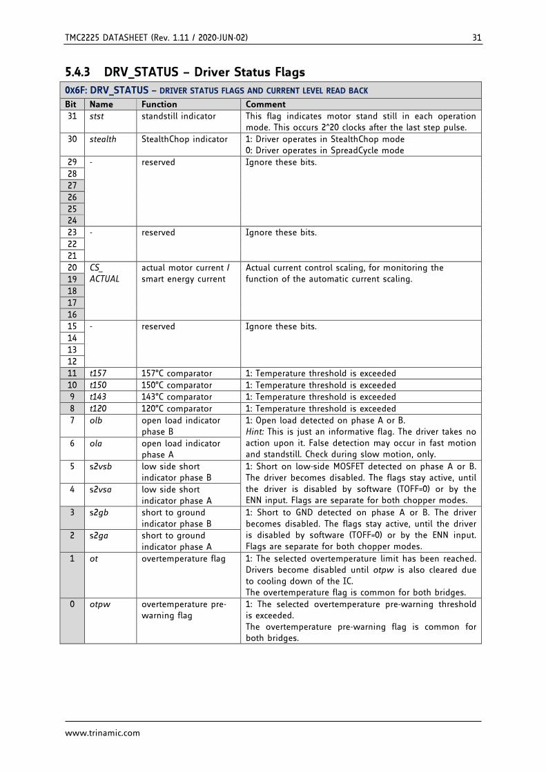
5.4.3 DRV_STATUS – Driver Status Flags
0X6F: DRV_STATUS – DRIVER STATUS FLAGS AND CURRENT LEVEL READ BACK
Bit Name Function Comment
31 stst standstill indicator This flag indicates motor stand still in each operation mode. This occurs 2^20 clocks after the last step pulse.
30 stealth StealthChop indicator 1: Driver operates in StealthChop mode 0: Driver operates in SpreadCycle mode
29 - reserved Ignore these bits.
28
27
26
25
24
23 - reserved Ignore these bits.
22
21
20 CS_ ACTUAL
actual motor current / smart energy current
Actual current control scaling, for monitoring the function of the automatic current scaling. 19
18
17
16
15 - reserved Ignore these bits.
14
13
12
11 t157 157°C comparator 1: Temperature threshold is exceeded
10 t150 150°C comparator 1: Temperature threshold is exceeded
9 t143 143°C comparator 1: Temperature threshold is exceeded
8 t120 120°C comparator 1: Temperature threshold is exceeded
7 olb open load indicator phase B
1: Open load detected on phase A or B. Hint: This is just an informative flag. The driver takes no action upon it. False detection may occur in fast motion and standstill. Check during slow motion, only.
6 ola open load indicator phase A
5 s2vsb low side short indicator phase B
1: Short on low-side MOSFET detected on phase A or B. The driver becomes disabled. The flags stay active, until the driver is disabled by software (TOFF=0) or by the ENN input. Flags are separate for both chopper modes.
4 s2vsa low side short indicator phase A
3 s2gb short to ground indicator phase B
1: Short to GND detected on phase A or B. The driver becomes disabled. The flags stay active, until the driver is disabled by software (TOFF=0) or by the ENN input. Flags are separate for both chopper modes.
2 s2ga short to ground indicator phase A
1 ot overtemperature flag 1: The selected overtemperature limit has been reached. Drivers become disabled until otpw is also cleared due to cooling down of the IC. The overtemperature flag is common for both bridges.
0 otpw overtemperature pre-warning flag
1: The selected overtemperature pre-warning threshold is exceeded. The overtemperature pre-warning flag is common for both bridges.

TMC2225 DATASHEET (Rev. 1.11 / 2020-JUN-02) 32
www.trinamic.com
6 StealthChop™ StealthChop is an extremely quiet mode of operation for stepper motors. It is based on a voltage mode PWM. In case of standstill and at low velocities, the motor is absolutely noiseless. Thus, StealthChop operated stepper motor applications are very suitable for indoor or home use. The motor operates absolutely free of vibration at low velocities. With StealthChop, the motor current is applied by driving a certain effective voltage into
the coil, using a voltage mode PWM. With the enhanced StealthChop2, the driver automatically adapts to the application for best performance. No more configurations are required. Optional configuration allows for tuning the setting in special cases, or for storing initial values for the automatic adaptation algorithm. For high velocity drives consider SpreadCycle in combination with StealthChop.
Figure 6.1 Motor coil sine wave current with StealthChop (measured with current probe)
6.1 Automatic Tuning StealthChop2 integrates an automatic tuning procedure (AT), which adapts the most important operating parameters to the motor automatically. This way, StealthChop2 allows high motor dynamics and supports powering down the motor to very low currents. Just two steps have to be respected by the motion controller for best results: Start with the motor in standstill, but powered with nominal run current (AT#1). Move the motor at a medium velocity, e.g. as part of a homing procedure (AT#2). Figure 6.2 shows the tuning procedure. Border conditions in for AT#1 and AT#2 are shown in the following table:
AUTOMATIC TUNING TIMING AND BORDER CONDITIONS
Step Parameter Conditions Duration
AT#1
PWM_ OFS_AUTO
- Motor in standstill and actual current scale (CS) is identical to run current (IRUN).
- If standstill reduction is enabled (pin PDN_UART=0), an initial step pulse switches the drive back to run current.
- Pins VS and VREF at operating level.
≤ 2^20+2*2^18 tCLK, ≤ 130ms (with internal clock)
AT#2
PWM_ GRAD_AUTO
- Motor must move at a velocity, where a significant amount of back EMF is generated and where the full run current can be reached. Conditions:
- 1.5 * PWM_OFS_AUTO < PWM_SCALE_SUM < 4 * PWM_OFS_AUTO
- PWM_SCALE_SUM < 255. Hint: A typical range is 60-300 RPM. Determine best conditions with the evaluation board and monitor PWM_SCALE_AUTO going down to zero during tuning.
8 fullsteps are required for a change of +/-1. For a typical motor with PWM_GRAD_AUTO optimum at 64 or less, up to 400 fullsteps are required when starting from OTP default 14.

TMC2225 DATASHEET (Rev. 1.11 / 2020-JUN-02) 33
www.trinamic.com
Determine best conditions for automatic tuning with the evaluation board. Monitor PWM_SCALE_AUTO going down to zero during the constant velocity phase in AT#2 tuning. This indicates a successful tuning.
Attention: Operating in StealthChop without proper tuning can lead to high motor currents during a deceleration ramp, especially with low resistive motors and fast deceleration settings. Follow the automatic tuning process and check optimum tuning conditions using the evaluation board. It is recommended to use an initial value for settings PWM_OFS and PWM_GRAD determined per motor type. Avoid hard stops from high velocities, even after tuning StealthChop settings. A deceleration ramp is required in each case. When powering up in StealthChop, make sure that the supply voltage ramps to the final voltage. Powering up to a lower voltage (e.g. 5V) will lead to wrong tuning, in case the motor becomes enabled at the lower voltage. Alternatively disable the motor during power-up.
Known Limitations: Successful completion of AT#1 tuning phase is not safely detected in all cases. It might require multiple motor start / stop events to safely detect completion. Successful determination is mandatory for AT#2: Tuning of PWM_GRAD will not start when AT#1 has not completed. Solution a): Complete automatic tuning phase AT#1 process, by using a slow-motion sequence which leads to standstill detection in between of each two steps. Use a velocity of 8 (6 Hz) or lower and execute minimum 10 steps during AT#1 phase. Solution b): Complete automatic tuning phase AT#1 process, by a doing sequence of four or more initial motions (using reduced acceleration, to match the fact that AT#2 has not yet completed) after power up. Make sure, that the driver is at standstill more than 130ms in between of each two motions. Solution c): Store application specific PWM_GRAD to OTP memory. Or, store initial parameters for PWM_GRAD_AUTO for the application and initialize by UART interface. Therefore, use the motor and operating conditions determined for the application and do a complete automatic tuning sequence (refer to a)). Note the resulting PWM_GRAD_AUTO value and use it for initialization of PWM_GRAD, or program the value to OTP memory. With this, tuning of AT#2 phase is not mandatory in the application and can be skipped. Automatic tuning will optimize settings during further operation. Combine with a) if desired.
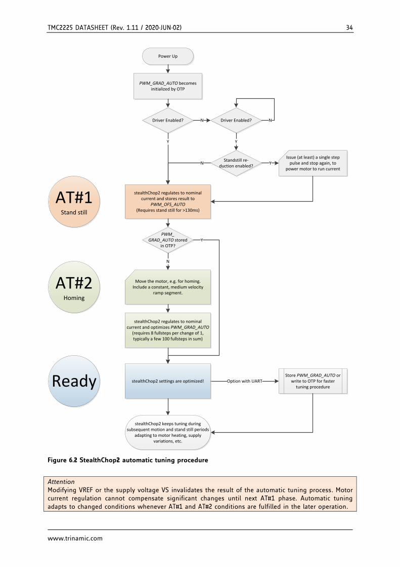
TMC2225 DATASHEET (Rev. 1.11 / 2020-JUN-02) 34
www.trinamic.com
AT#1Stand still
AT#2Homing
Ready
Power Up
stealthChop2 regulates to nominal current and stores result to
PWM_OFS_AUTO(Requires stand still for >130ms)
N
PWM_GRAD_AUTO becomes initialized by OTP
Driver Enabled? N
Standstill re- duction enabled?
Y
Issue (at least) a single step pulse and stop again, to
power motor to run currentY
Driver Enabled? N
Y
Move the motor, e.g. for homing. Include a constant, medium velocity
ramp segment.
Store PWM_GRAD_AUTO or write to OTP for faster
tuning procedureOption with UART
PWM_GRAD_AUTO stored
in OTP?
N
Y
stealthChop2 regulates to nominal current and optimizes PWM_GRAD_AUTO
(requires 8 fullsteps per change of 1, typically a few 100 fullsteps in sum)
stealthChop2 settings are optimized!
stealthChop2 keeps tuning during subsequent motion and stand still periods
adapting to motor heating, supply variations, etc.
Figure 6.2 StealthChop2 automatic tuning procedure
Attention Modifying VREF or the supply voltage VS invalidates the result of the automatic tuning process. Motor current regulation cannot compensate significant changes until next AT#1 phase. Automatic tuning adapts to changed conditions whenever AT#1 and AT#2 conditions are fulfilled in the later operation.

TMC2225 DATASHEET (Rev. 1.11 / 2020-JUN-02) 35
www.trinamic.com
6.2 StealthChop Options In order to match the motor current to a certain level, the effective PWM voltage becomes scaled depending on the actual motor velocity. Several additional factors influence the required voltage level to drive the motor at the target current: The motor resistance, its back EMF (i.e. directly proportional to its velocity) as well as the actual level of the supply voltage. Two modes of PWM regulation are provided: The automatic tuning mode (AT) using current feedback (pwm_autoscale = 1, pwm_autograd = 1) and a feed forward velocity-controlled mode (pwm_autoscale = 0). The feed forward velocity-controlled mode will not react to a change of the supply voltage or to events like a motor stall, but it provides very stable amplitude. It does not use nor require any means of current measurement. This is perfect when motor type and supply voltage are well known. Therefore, we recommend the automatic mode, unless current regulation is not satisfying in the given operating conditions.
It is recommended to operate in automatic tuning mode.
Non-automatic mode (pwm_autoscale=0) should be taken into account only with well-known motor and operating conditions. In this case, programming via the UART interface is required. The operating parameters PWM_GRAD and PWM_OFS can be determined in automatic tuning mode initially.
Hint: In non-automatic mode the power supply current directly reflects mechanical load on the motor.
The StealthChop PWM frequency can be chosen in four steps in order to adapt the frequency divider to the frequency of the clock source. A setting in the range of 20-50kHz is good for most applications. It balances low current ripple and good higher velocity performance vs. dynamic power dissipation.
CHOICE OF PWM FREQUENCY FOR STEALTHCHOP
Clock frequency fCLK
PWM_FREQ=%00 fPWM=2/1024 fCLK
PWM_FREQ=%01 fPWM=2/683 fCLK
(default)
PWM_FREQ=%10 fPWM=2/512 fCLK
(OTP option)
PWM_FREQ=%11 fPWM=2/410 fCLK
18MHz 35.2kHz 52.7kHz 70.3kHz 87.8kHz
16MHz 31.3kHz 46.9kHz 62.5kHz 78.0kHz
12MHz (internal) 23.4kHz 35.1kHz 46.9kHz 58.5kHz
10MHz 19.5kHz 29.3kHz 39.1kHz 48.8kHz
8MHz 15.6kHz 23.4kHz 31.2kHz 39.0kHz
Table 6.1 Choice of PWM frequency – green / light green: recommended
6.3 StealthChop Current Regulator In StealthChop voltage PWM mode, the autoscaling function (pwm_autoscale = 1, pwm_auto_grad = 1) regulates the motor current to the desired current setting. Automatic scaling is used as part of the automatic tuning process (AT), and for subsequent tracking of changes within the motor parameters. The driver measures the motor current during the chopper on time and uses a proportional regulator to regulate PWM_SCALE_AUTO in order match the motor current to the target current. PWM_REG is the proportionality coefficient for this regulator. Basically, the proportionality coefficient should be as small as possible in order to get a stable and soft regulation behavior, but it must be large enough to allow the driver to quickly react to changes caused by variation of the motor target current (e.g. change of VREF). During initial tuning step AT#2, PWM_REG also compensates for the change of motor velocity. Therefore, a high acceleration during AT#2 will require a higher setting of PWM_REG. With careful selection of homing velocity and acceleration, a minimum setting of the regulation gradient often is sufficient (PWM_REG=1). PWM_REG setting should be optimized for the fastest required acceleration and deceleration ramp (compare Figure 6.3 and Figure 6.4). The quality of the setting PWM_REG in phase AT#2 and the finished automatic tuning procedure (or non-automatic settings for PWM_OFS and PWM_GRAD) can be examined when monitoring motor current during an acceleration phase Figure 6.5.
UART
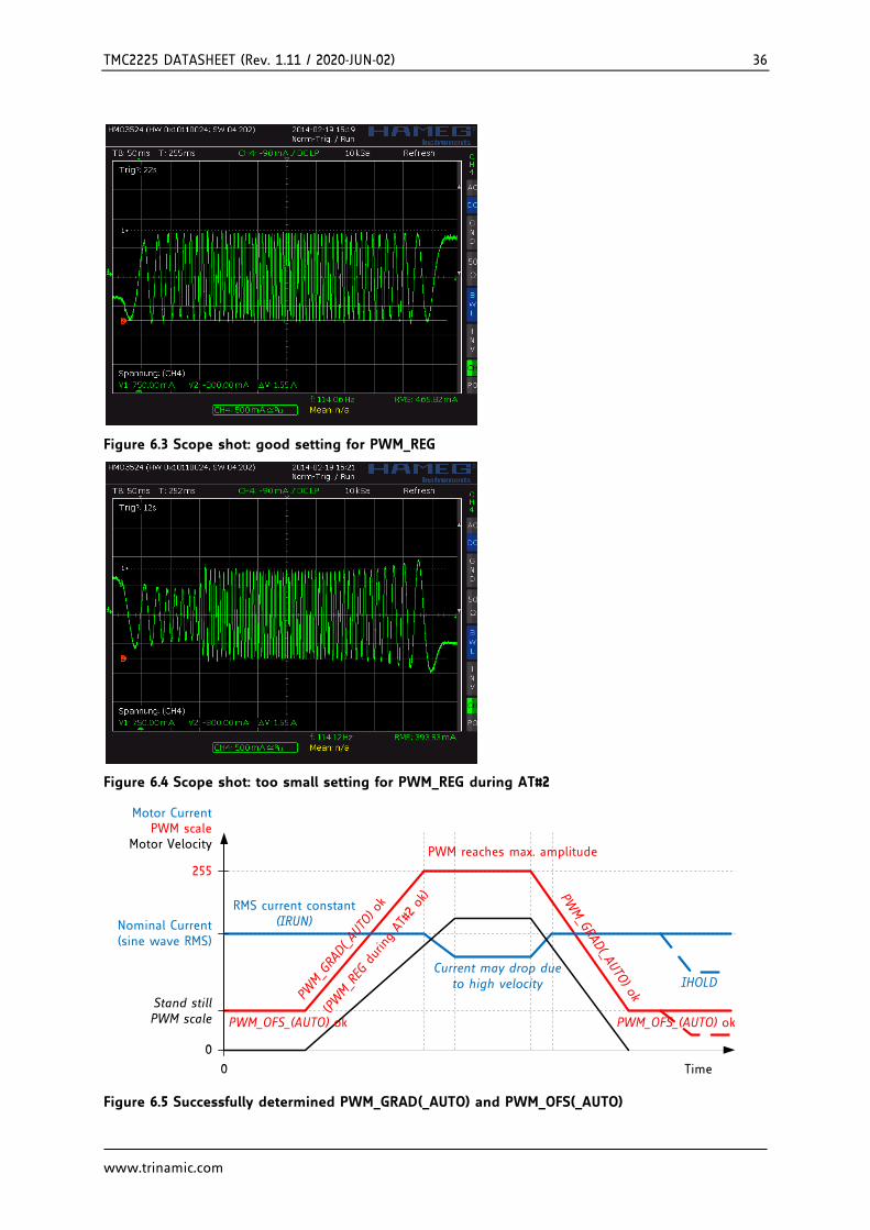
TMC2225 DATASHEET (Rev. 1.11 / 2020-JUN-02) 36
www.trinamic.com
Figure 6.3 Scope shot: good setting for PWM_REG
Figure 6.4 Scope shot: too small setting for PWM_REG during AT#2
Motor Velocity
Time
Stand still PWM scale
PWM reaches max. amplitude
255
0
Motor Current
Nominal Current(sine wave RMS)
RMS current constant (IRUN)
0
PWM scale
Current may drop due to high velocity
PWM_G
RAD(
_AUT
O) o
k
PWM_G
RAD(_AUTO
) ok
PWM_OFS_(AUTO) ok
(PWM_R
EG during AT
#2 o
k)
IHOLD
PWM_OFS_(AUTO) ok
Figure 6.5 Successfully determined PWM_GRAD(_AUTO) and PWM_OFS(_AUTO)
TMC2225 DATASHEET (Rev. 1.11 / 2020-JUN-02) 37
www.trinamic.com
Quick Start For a quick start, see the Quick Configuration Guide in chapter 14.
6.3.1 Lower Current Limit The StealthChop current regulator imposes a lower limit for motor current regulation. As the coil current can be measured in the shunt resistor during chopper on phase only, a minimum chopper duty cycle allowing coil current regulation is given by the blank time as set by TBL and by the chopper frequency setting. Therefore, the motor specific minimum coil current in StealthChop autoscaling mode rises with the supply voltage and with the chopper frequency. A lower blanking time allows a lower current limit. It is important for the correct determination of PWM_OFS_AUTO, that in AT#1 the run current set by the sense resistor, VREF and IRUN is well within the regulation range. Lower currents (e.g. for standstill power down) are automatically realized based on PWM_OFS_AUTO and PWM_GRAD_AUTO respectively based on PWM_OFS and PWM_GRAD with non-automatic current scaling. The freewheeling option allows going to zero motor current. Lower motor coil current limit for StealthChop2 automatic tuning:
𝐼𝐿𝑜𝑤𝑒𝑟 𝐿𝑖𝑚𝑖𝑡 = 𝑡𝐵𝐿𝐴𝑁𝐾 ∗ 𝑓𝑃𝑊𝑀 ∗𝑉𝑀
𝑅𝐶𝑂𝐼𝐿
With VM the motor supply voltage and RCOIL the motor coil resistance. ILower Limit can be treated as a thumb value for the minimum nominal IRUN motor current setting.
EXAMPLE: A motor has a coil resistance of 5Ω, the supply voltage is 24V. With TBL=%01 and PWM_FREQ=%00, tBLANK is 24 clock cycles, fPWM is 2/(1024 clock cycles):
𝐼𝐿𝑜𝑤𝑒𝑟 𝐿𝑖𝑚𝑖𝑡 = 24 𝑡𝐶𝐿𝐾 ∗2
1024 𝑡𝐶𝐿𝐾
∗24𝑉
5Ω=
24
512∗
24𝑉
5Ω= 225𝑚𝐴
This means, the motor target current for automatic tuning must be 225mA or more, taking into account all relevant settings. This lower current limit also applies for modification of the motor current via the analog input VREF.
Attention For automatic tuning, a lower coil current limit applies. The motor current in automatic tuning phase AT#1 must exceed this lower limit. ILOWER LIMIT can be calculated or measured using a current probe. Setting the motor run-current or hold-current below the lower current limit during operation by modifying IRUN and IHOLD is possible after successful automatic tuning. The lower current limit also limits the capability of the driver to respond to changes of VREF.
6.4 Velocity Based Scaling Velocity based scaling scales the StealthChop amplitude based on the time between each two steps, i.e. based on TSTEP, measured in clock cycles. This concept basically does not require a current measurement, because no regulation loop is necessary. A pure velocity-based scaling is available via UART programming, only, when setting pwm_autoscale = 0. The basic idea is to have a linear approximation of the voltage required to drive the target current into the motor. The stepper motor has a certain coil resistance and thus needs a certain voltage amplitude to yield a target current based on the basic formula I=U/R. With R being the coil resistance, U the supply voltage scaled by the PWM value, the current I results. The initial value for PWM_AMPL can be calculated:
UART

TMC2225 DATASHEET (Rev. 1.11 / 2020-JUN-02) 38
www.trinamic.com
𝑃𝑊𝑀_𝐴𝑀𝑃𝐿 =374 ∗ 𝑅𝐶𝑂𝐼𝐿 ∗ 𝐼𝐶𝑂𝐼𝐿
𝑉𝑀
With VM the motor supply voltage and ICOIL the target RMS current The effective PWM voltage UPWM (1/SQRT(2) x peak value) results considering the 8 bit resolution and 248 sine wave peak for the actual PWM amplitude shown as PWM_SCALE:
𝑈𝑃𝑊𝑀 = 𝑉𝑀 ∗𝑃𝑊𝑀_𝑆𝐶𝐴𝐿𝐸
256∗
248
256∗
1
√2= 𝑉𝑀 ∗
𝑃𝑊𝑀_𝑆𝐶𝐴𝐿𝐸
374
With rising motor velocity, the motor generates an increasing back EMF voltage. The back EMF voltage is proportional to the motor velocity. It reduces the PWM voltage effective at the coil resistance and thus current decreases. The TMC2225 provides a second velocity dependent factor (PWM_GRAD) to compensate for this. The overall effective PWM amplitude (PWM_SCALE_SUM) in this mode automatically is calculated in dependence of the microstep frequency as:
𝑃𝑊𝑀_𝑆𝐶𝐴𝐿𝐸_𝑆𝑈𝑀 = 𝑃𝑊𝑀_𝑂𝐹𝑆 + 𝑃𝑊𝑀_𝐺𝑅𝐴𝐷 ∗ 256 ∗𝑓𝑆𝑇𝐸𝑃
𝑓𝐶𝐿𝐾
With fSTEP being the microstep frequency for 256 microstep resolution equivalent and fCLK the clock frequency supplied to the driver or the actual internal frequency As a first approximation, the back EMF subtracts from the supply voltage and thus the effective current amplitude decreases. This way, a first approximation for PWM_GRAD setting can be calculated:
𝑃𝑊𝑀_𝐺𝑅𝐴𝐷 = 𝐶𝐵𝐸𝑀𝐹 [𝑉
𝑟𝑎𝑑𝑠
] ∗ 2𝜋 ∗𝑓𝐶𝐿𝐾 ∗ 1.46
𝑉𝑀 ∗ 𝑀𝑆𝑃𝑅
CBEMF is the back EMF constant of the motor in Volts per radian/second. MSPR is the number of microsteps per rotation, e.g. 51200 = 256µsteps multiplied by 200 fullsteps for a 1.8° motor.
PWM scaling(PWM_SCALE_SUM)
Velocity
PWM_OFS
PWM reaches max. amplitude
255
0
PWM_G
RAD
Motor current
Nominal current(e.g. sine wave RMS)
Current drops (depends on
motor load)
Constant motor RMS current
0
VPWMMAX
Figure 6.6 Velocity based PWM scaling (pwm_autoscale=0)
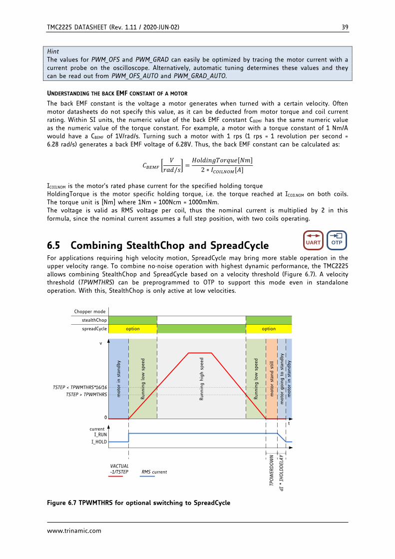
TMC2225 DATASHEET (Rev. 1.11 / 2020-JUN-02) 39
www.trinamic.com
Hint The values for PWM_OFS and PWM_GRAD can easily be optimized by tracing the motor current with a current probe on the oscilloscope. Alternatively, automatic tuning determines these values and they can be read out from PWM_OFS_AUTO and PWM_GRAD_AUTO.
UNDERSTANDING THE BACK EMF CONSTANT OF A MOTOR
The back EMF constant is the voltage a motor generates when turned with a certain velocity. Often motor datasheets do not specify this value, as it can be deducted from motor torque and coil current rating. Within SI units, the numeric value of the back EMF constant CBEMF has the same numeric value as the numeric value of the torque constant. For example, a motor with a torque constant of 1 Nm/A would have a CBEMF of 1V/rad/s. Turning such a motor with 1 rps (1 rps = 1 revolution per second = 6.28 rad/s) generates a back EMF voltage of 6.28V. Thus, the back EMF constant can be calculated as:
𝐶𝐵𝐸𝑀𝐹 [𝑉
𝑟𝑎𝑑/𝑠] =
𝐻𝑜𝑙𝑑𝑖𝑛𝑔𝑇𝑜𝑟𝑞𝑢𝑒[𝑁𝑚]
2 ∗ 𝐼𝐶𝑂𝐼𝐿𝑁𝑂𝑀[𝐴]
ICOILNOM is the motor’s rated phase current for the specified holding torque HoldingTorque is the motor specific holding torque, i.e. the torque reached at ICOILNOM on both coils. The torque unit is [Nm] where 1Nm = 100Ncm = 1000mNm. The voltage is valid as RMS voltage per coil, thus the nominal current is multiplied by 2 in this formula, since the nominal current assumes a full step position, with two coils operating.
6.5 Combining StealthChop and SpreadCycle For applications requiring high velocity motion, SpreadCycle may bring more stable operation in the upper velocity range. To combine no-noise operation with highest dynamic performance, the TMC2225 allows combining StealthChop and SpreadCycle based on a velocity threshold (Figure 6.7). A velocity threshold (TPWMTHRS) can be preprogrammed to OTP to support this mode even in standalone operation. With this, StealthChop is only active at low velocities.
Runnin
g low
speed
optionoption
Runnin
g low
speed
Runnin
g h
igh s
peed
moto
r st
and s
till
moto
r goin
g to s
tandby
moto
r in
sta
ndby
moto
r in
sta
ndby
v
t
TSTEP < TPWMTHRS*16/16
TSTEP > TPWMTHRS
0
VACTUAL~1/TSTEP
current
TPOW
ERDOW
N
RMS current
I_HOLD
I_RUN
dI
* IH
OLD
DEL
AY
stealthChop
spreadCycle
Chopper mode
TRINAMIC, B. Dwersteg, 14.3.14
Figure 6.7 TPWMTHRS for optional switching to SpreadCycle
UART OTP

TMC2225 DATASHEET (Rev. 1.11 / 2020-JUN-02) 40
www.trinamic.com
As a first step, both chopper principles should be parameterized and optimized individually (SpreadCycle settings may be programmed to OTP memory). In a next step, a transfer velocity has to be fixed. For example, StealthChop operation is used for precise low speed positioning, while SpreadCycle shall be used for highly dynamic motion. TPWMTHRS determines the transition velocity. Read out TSTEP when moving at the desired velocity and program the resulting value to TPWMTHRS. Use a low transfer velocity to avoid a jerk at the switching point.
A jerk occurs when switching at higher velocities, because the back-EMF of the motor (which rises with the velocity) causes a phase shift of up to 90° between motor voltage and motor current. So when switching at higher velocities between voltage PWM and current PWM mode, this jerk will occur with increased intensity. A high jerk may even produce a temporary overcurrent condition (depending on the motor coil resistance). At low velocities (e.g. 1 to a few 10 RPM), it can be completely neglected for most motors. Therefore, consider the switching jerk when choosing TPWMTHRS. Set TPWMTHRS zero if you want to work with StealthChop only.
When enabling the StealthChop mode the first time using automatic current regulation, the motor must be at stand still in order to allow a proper current regulation. When the drive switches to StealthChop at a higher velocity, StealthChop logic stores the last current regulation setting until the motor returns to a lower velocity again. This way, the regulation has a known starting point when returning to a lower velocity, where StealthChop becomes re-enabled. Therefore, neither the velocity threshold nor the supply voltage must be considerably changed during the phase while the chopper is switched to a different mode, because otherwise the motor might lose steps or the instantaneous current might be too high or too low.
A motor stall or a sudden change in the motor velocity may lead to the driver detecting a short circuit or to a state of automatic current regulation, from which it cannot recover. Clear the error flags and restart the motor from zero velocity to recover from this situation.
Hint Start the motor from standstill when switching on StealthChop the first time and keep it stopped for at least 128 chopper periods to allow StealthChop to do initial standstill current control.
6.6 Flags in StealthChop As StealthChop uses voltage mode driving, status flags based on current measurement respond slower, respectively the driver reacts delayed to sudden changes of back EMF, like on a motor stall.
Attention A motor stall, or abrupt stop of the motion during operation in StealthChop can trigger an overcurrent condition. Depending on the previous motor velocity, and on the coil resistance of the motor, it significantly increases motor current for a time of several 10ms. With low velocities, where the back EMF is just a fraction of the supply voltage, there is no danger of triggering the short detection.
6.6.1 Open Load Flags In StealthChop mode, status information is different from the cycle-by-cycle regulated SpreadCycle mode. OLA and OLB show if the current regulation sees that the nominal current can be reached on both coils.
- A flickering OLA or OLB can result from asymmetries in the sense resistors or in the motor coils.
- An interrupted motor coil leads to a continuously active open load flag for the coil. - One or both flags are active, if the current regulation did not succeed in scaling up to the full
target current within the last few fullsteps (because no motor is attached or a high velocity exceeds the PWM limit).
If desired, do an on-demand open load test using the SpreadCycle chopper, as it delivers the safest result. With StealthChop, PWM_SCALE_SUM can be checked to detect the correct coil resistance.
UART

TMC2225 DATASHEET (Rev. 1.11 / 2020-JUN-02) 41
www.trinamic.com
6.6.2 PWM_SCALE_SUM Informs about the Motor State Information about the motor state is available with automatic scaling by reading out PWM_SCALE_SUM. As this parameter reflects the actual voltage required to drive the target current into the motor, it depends on several factors: motor load, coil resistance, supply voltage, and current setting. Therefore, an evaluation of the PWM_SCALE_SUM value allows checking the motor operation point. When reaching the limit (255), the current regulator cannot sustain the full motor current, e.g. due to a drop in supply voltage.
6.7 Freewheeling and Passive Braking StealthChop provides different options for motor standstill. These options can be enabled by setting the standstill current IHOLD to zero and choosing the desired option using the FREEWHEEL setting. The desired option becomes enabled after a time period specified by TPOWERDOWN and IHOLD_DELAY. Current regulation becomes frozen once the motor target current is at zero current in order to ensure a quick startup. With the freewheeling options, both freewheeling and passive braking can be realized. Passive braking is an effective eddy current motor braking, which consumes a minimum of energy, because no active current is driven into the coils. However, passive braking will allow slow turning of the motor when a continuous torque is applied.
Hint Operate the motor within your application when exploring StealthChop. Motor performance often is better with a mechanical load, because it prevents the motor from stalling due mechanical oscillations which can occur without load.
UART
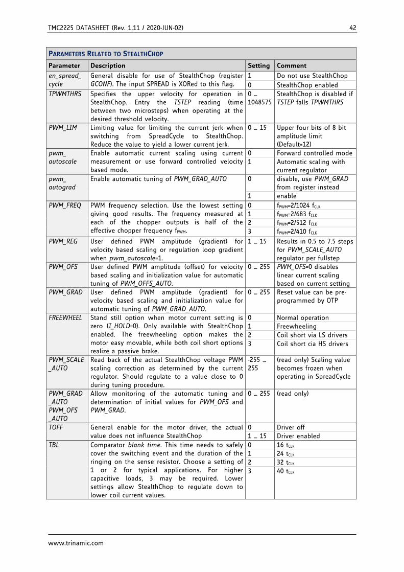
TMC2225 DATASHEET (Rev. 1.11 / 2020-JUN-02) 42
www.trinamic.com
PARAMETERS RELATED TO STEALTHCHOP
Parameter Description Setting Comment
en_spread_ cycle
General disable for use of StealthChop (register GCONF). The input SPREAD is XORed to this flag.
1 Do not use StealthChop
0 StealthChop enabled
TPWMTHRS Specifies the upper velocity for operation in StealthChop. Entry the TSTEP reading (time between two microsteps) when operating at the desired threshold velocity.
0 … 1048575
StealthChop is disabled if TSTEP falls TPWMTHRS
PWM_LIM Limiting value for limiting the current jerk when switching from SpreadCycle to StealthChop. Reduce the value to yield a lower current jerk.
0 … 15 Upper four bits of 8 bit amplitude limit (Default=12)
pwm_ autoscale
Enable automatic current scaling using current measurement or use forward controlled velocity based mode.
0 Forward controlled mode
1 Automatic scaling with current regulator
pwm_ autograd
Enable automatic tuning of PWM_GRAD_AUTO 0 disable, use PWM_GRAD from register instead
1 enable
PWM_FREQ PWM frequency selection. Use the lowest setting giving good results. The frequency measured at each of the chopper outputs is half of the effective chopper frequency fPWM.
0 fPWM=2/1024 fCLK
1 fPWM=2/683 fCLK
2 fPWM=2/512 fCLK
3 fPWM=2/410 fCLK
PWM_REG User defined PWM amplitude (gradient) for velocity based scaling or regulation loop gradient when pwm_autoscale=1.
1 … 15 Results in 0.5 to 7.5 steps for PWM_SCALE_AUTO regulator per fullstep
PWM_OFS User defined PWM amplitude (offset) for velocity based scaling and initialization value for automatic tuning of PWM_OFFS_AUTO.
0 … 255 PWM_OFS=0 disables linear current scaling based on current setting
PWM_GRAD User defined PWM amplitude (gradient) for velocity based scaling and initialization value for automatic tuning of PWM_GRAD_AUTO.
0 … 255 Reset value can be pre-programmed by OTP
FREEWHEEL Stand still option when motor current setting is zero (I_HOLD=0). Only available with StealthChop enabled. The freewheeling option makes the motor easy movable, while both coil short options realize a passive brake.
0 Normal operation
1 Freewheeling
2 Coil short via LS drivers
3 Coil short cia HS drivers
PWM_SCALE _AUTO
Read back of the actual StealthChop voltage PWM scaling correction as determined by the current regulator. Should regulate to a value close to 0 during tuning procedure.
-255 … 255
(read only) Scaling value becomes frozen when operating in SpreadCycle
PWM_GRAD _AUTO PWM_OFS _AUTO
Allow monitoring of the automatic tuning and determination of initial values for PWM_OFS and PWM_GRAD.
0 … 255
(read only)
TOFF General enable for the motor driver, the actual value does not influence StealthChop
0 Driver off
1 … 15 Driver enabled
TBL Comparator blank time. This time needs to safely cover the switching event and the duration of the ringing on the sense resistor. Choose a setting of 1 or 2 for typical applications. For higher capacitive loads, 3 may be required. Lower settings allow StealthChop to regulate down to lower coil current values.
0 16 tCLK
1 24 tCLK
2 32 tCLK
3 40 tCLK

TMC2225 DATASHEET (Rev. 1.11 / 2020-JUN-02) 43
www.trinamic.com
7 SpreadCycle Chopper While StealthChop is a voltage mode PWM controlled chopper, SpreadCycle is a cycle-by-cycle current control. Therefore, it can react extremely fast to changes in motor velocity or motor load. SpreadCycle will give better performance in medium to high velocity range for motors and applications which tend to resonance. The currents through both motor coils are controlled using choppers. The choppers work independently of each other. In Figure 7.1 the different chopper phases are shown.
RSENSE
ICOIL
On Phase: current flows in direction of target current
RSENSE
ICOIL
Fast Decay Phase: current flows in opposite direction of target current
RSENSE
ICOIL
Slow Decay Phase: current re-circulation
+VM +VM +VM
Figure 7.1 Chopper phases
Although the current could be regulated using only on phases and fast decay phases, insertion of the slow decay phase is important to reduce electrical losses and current ripple in the motor. The duration of the slow decay phase is specified in a control parameter and sets an upper limit on the chopper frequency. The current comparator can measure coil current during phases when the current flows through the sense resistor, but not during the slow decay phase, so the slow decay phase is terminated by a timer. The on phase is terminated by the comparator when the current through the coil reaches the target current. The fast decay phase may be terminated by either the comparator or another timer.
When the coil current is switched, spikes at the sense resistors occur due to charging and discharging parasitic capacitances. During this time, typically one or two microseconds, the current cannot be measured. Blanking is the time when the input to the comparator is masked to block these spikes.
The SpreadCycle chopper mode cycles through four phases: on, slow decay, fast decay, and a second slow decay.
The chopper frequency is an important parameter for a chopped motor driver. A too low frequency might generate audible noise. A higher frequency reduces current ripple in the motor, but with a too high frequency magnetic losses may rise. Also power dissipation in the driver rises with increasing frequency due to the increased influence of switching slopes causing dynamic dissipation. Therefore, a compromise needs to be found. Most motors are optimally working in a frequency range of 16 kHz to 30 kHz. The chopper frequency is influenced by a number of parameter settings as well as by the motor inductivity and supply voltage.
Hint A chopper frequency in the range of 16 kHz to 30 kHz gives a good result for most motors when using SpreadCycle. A higher frequency leads to increased switching losses.
TMC2225 DATASHEET (Rev. 1.11 / 2020-JUN-02) 44
www.trinamic.com
7.1 SpreadCycle Settings The SpreadCycle (patented) chopper algorithm is a precise and simple to use chopper mode which automatically determines the optimum length for the fast-decay phase. The SpreadCycle will provide superior microstepping quality even with default settings. Several parameters are available to optimize the chopper to the application. Each chopper cycle is comprised of an on phase, a slow decay phase, a fast decay phase and a second slow decay phase (see Figure 7.3). The two slow decay phases and the two blank times per chopper cycle put an upper limit to the chopper frequency. The slow decay phases typically make up for about 30%-70% of the chopper cycle in standstill and are important for low motor and driver power dissipation. Calculation of a starting value for the slow decay time TOFF:
EXAMPLE: Target Chopper frequency: 25kHz. Assumption: Two slow decay cycles make up for 50% of overall chopper cycle time
𝑡𝑂𝐹𝐹 =1
25𝑘𝐻𝑧∗
50
100∗
1
2= 10µ𝑠
For the TOFF setting this means: 𝑇𝑂𝐹𝐹 = (𝑡𝑂𝐹𝐹 ∗ 𝑓𝐶𝐿𝐾 − 24)/32
With 12 MHz clock this gives a setting of TOFF=3.0, i.e. 3. With 16 MHz clock this gives a setting of TOFF=4.25, i.e. 4 or 5.
The hysteresis start setting forces the driver to introduce a minimum amount of current ripple into the motor coils. The current ripple must be higher than the current ripple which is caused by resistive losses in the motor in order to give best microstepping results. This will allow the chopper to precisely regulate the current both for rising and for falling target current. The time required to introduce the current ripple into the motor coil also reduces the chopper frequency. Therefore, a higher hysteresis setting will lead to a lower chopper frequency. The motor inductance limits the ability of the chopper to follow a changing motor current. Further the duration of the on phase and the fast decay must be longer than the blanking time, because the current comparator is disabled during blanking. It is easiest to find the best setting by starting from a low hysteresis setting (e.g. HSTRT=0, HEND=0) and increasing HSTRT, until the motor runs smoothly at low velocity settings. This can best be checked when measuring the motor current either with a current probe or by probing the sense resistor voltages (see Figure 7.2). Checking the sine wave shape near zero transition will show a small ledge between both half waves in case the hysteresis setting is too small. At medium velocities (i.e. 100 to 400 fullsteps per second), a too low hysteresis setting will lead to increased humming and vibration of the motor.
UART OTP

TMC2225 DATASHEET (Rev. 1.11 / 2020-JUN-02) 45
www.trinamic.com
Figure 7.2 No ledges in current wave with sufficient hysteresis (magenta: current A, yellow & blue: sense resistor voltages A and B)
A too high hysteresis setting will lead to reduced chopper frequency and increased chopper noise but will not yield any benefit for the wave shape.
Quick Start For a quick start, see the Quick Configuration Guide in chapter 14. For detail procedure see Application Note AN001 - Parameterization of SpreadCycle
As experiments show, the setting is quite independent of the motor, because higher current motors typically also have a lower coil resistance. Therefore choosing a low to medium default value for the hysteresis (for example, effective hysteresis = 4) normally fits most applications. The setting can be optimized by experimenting with the motor: A too low setting will result in reduced microstep accuracy, while a too high setting will lead to more chopper noise and motor power dissipation. When measuring the sense resistor voltage in motor standstill at a medium coil current with an oscilloscope, a too low setting shows a fast decay phase not longer than the blanking time. When the fast decay time becomes slightly longer than the blanking time, the setting is optimum. You can reduce the off-time setting, if this is hard to reach. The hysteresis principle could in some cases lead to the chopper frequency becoming too low, e.g. when the coil resistance is high when compared to the supply voltage. This is avoided by splitting the hysteresis setting into a start setting (HSTRT+HEND) and an end setting (HEND). An automatic hysteresis decrementer (HDEC) interpolates between both settings, by decrementing the hysteresis value stepwise each 16 system clocks. At the beginning of each chopper cycle, the hysteresis begins with a value which is the sum of the start and the end values (HSTRT+HEND), and decrements during the cycle, until either the chopper cycle ends or the hysteresis end value (HEND) is reached. This way, the chopper frequency is stabilized at high amplitudes and low supply voltage situations, if the frequency gets too low. This avoids the frequency reaching the audible range.
Hint Highest motor velocities sometimes benefit from setting TOFF to 1 or 2 and a short TBL of 1 or 0.
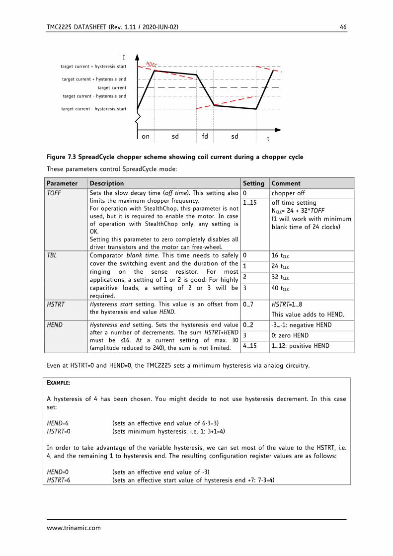
TMC2225 DATASHEET (Rev. 1.11 / 2020-JUN-02) 46
www.trinamic.com
t
I
target current
target current - hysteresis start
target current + hysteresis start
on sd fd sd
target current + hysteresis end
target current - hysteresis end
HDEC
Figure 7.3 SpreadCycle chopper scheme showing coil current during a chopper cycle
These parameters control SpreadCycle mode:
Even at HSTRT=0 and HEND=0, the TMC2225 sets a minimum hysteresis via analog circuitry.
EXAMPLE: A hysteresis of 4 has been chosen. You might decide to not use hysteresis decrement. In this case set: HEND=6 (sets an effective end value of 6-3=3) HSTRT=0 (sets minimum hysteresis, i.e. 1: 3+1=4) In order to take advantage of the variable hysteresis, we can set most of the value to the HSTRT, i.e. 4, and the remaining 1 to hysteresis end. The resulting configuration register values are as follows: HEND=0 (sets an effective end value of -3) HSTRT=6 (sets an effective start value of hysteresis end +7: 7-3=4)
Parameter Description Setting Comment
TOFF Sets the slow decay time (off time). This setting also limits the maximum chopper frequency. For operation with StealthChop, this parameter is not used, but it is required to enable the motor. In case of operation with StealthChop only, any setting is OK. Setting this parameter to zero completely disables all driver transistors and the motor can free-wheel.
0 chopper off
1…15 off time setting NCLK= 24 + 32*TOFF (1 will work with minimum blank time of 24 clocks)
TBL Comparator blank time. This time needs to safely cover the switching event and the duration of the ringing on the sense resistor. For most applications, a setting of 1 or 2 is good. For highly capacitive loads, a setting of 2 or 3 will be required.
0 16 tCLK
1 24 tCLK
2 32 tCLK
3 40 tCLK
HSTRT Hysteresis start setting. This value is an offset from the hysteresis end value HEND.
0…7 HSTRT=1…8
This value adds to HEND.
HEND Hysteresis end setting. Sets the hysteresis end value after a number of decrements. The sum HSTRT+HEND must be ≤16. At a current setting of max. 30 (amplitude reduced to 240), the sum is not limited.
0…2 -3…-1: negative HEND
3 0: zero HEND
4…15 1…12: positive HEND

TMC2225 DATASHEET (Rev. 1.11 / 2020-JUN-02) 47
www.trinamic.com
8 Selecting Sense Resistors Set the desired maximum motor current by selecting an appropriate value for the sense resistor. The following table shows the RMS current values which can be reached using standard resistors and motor types fitting without additional motor current scaling.
CHOICE OF RSENSE AND RESULTING MAX. MOTOR CURRENT
RSENSE [Ω] RMS current [A] VREF=2.5V (or open), IRUN=31, vsense=0 (standard)
Fitting motor type (examples)
1.00 0.22
300mA motor
0.82 0.27
0.75 0.29
0.68 0.32 400mA motor
0.50 0.43
500mA motor 470m 0.46
390m 0.55 600mA motor
330m 0.64 700mA motor
270m 0.77 800mA motor
220m 0.92 1A motor
180m 1.09 1.2A motor
150m 1.28
1.5A motor
120m 1.53*)
100m 1.77*)
*) Value exceeds upper current rating, scaling down required, e.g. by reduced VREF. Sense resistors should be carefully selected. The full motor current flows through the sense resistors. Due to chopper operation the sense resistors see pulsed current from the MOSFET bridges. Therefore, a low-inductance type such as film or composition resistors is required to prevent voltage spikes causing ringing on the sense voltage inputs leading to unstable measurement results. Also, a low-inductance, low-resistance PCB layout is essential. Any common GND path for the two sense resistors must be avoided, because this would lead to coupling between the two current sense signals. A massive ground plane is best. Please also refer to layout considerations in chapter 19.
The sense resistor needs to be able to conduct the peak motor coil current in motor standstill conditions, unless standby power is reduced. Under normal conditions, the sense resistor conducts less than the coil RMS current, because no current flows through the sense resistor during the slow decay phases. A 0.5W type is sufficient for most applications up to 1.2A RMS current.
Attention Be sure to use a symmetrical sense resistor layout and short and straight sense resistor traces of identical length. Well matching sense resistors ensure best performance. A compact layout with massive ground plane is best to avoid parasitic resistance effects.
TMC2225 DATASHEET (Rev. 1.11 / 2020-JUN-02) 48
www.trinamic.com
9 Motor Current Control The basic motor current is set by the resistance of the sense resistors. Several possibilities allow scaling down motor current, e.g. to adapt for different motors, or to reduce motor current in standstill or low load situations.
METHODS FOR SCALING MOTOR CURRENT
Method Parameters Range Primary Use
Pin VREF voltage (chapter 9.1)
VREF input scales IRUN and IHOLD. Can be disabled by GCONF.i_scale_analog
2.5V: 100% … 0.5V: 20% >2.5V or open: 100% <0.5V: not recommended
- Fine tuning of motor current to fit the motor type
- Manual tuning via poti - Delayed or soft power-up - Standstill current reduction
(preferred only with SpreadCycle)
Pin ENN Disable / enable driver stage
0: Motor enable 1: Motor disable
- Disable motor to allow freewheeling
Pin PDN_UART Disable / enable standstill current reduction to IHOLD
0: Standstill current reduction enabled. 1: Disable
- Enable current reduction to reduce heat up in stand still
OTP memory OTP_IHOLD, OTP_IHOLDDELAY
9% to 78% standby current. Reduction in about 300ms to 2.5s
- Program current reduction to fit application for highest efficiency and lowest heat up
OTP memory otp_internalRsense 0: Use sense resistors 1: Internal resistors
- Save two sense resistors on BOM, set current by single inexpensive 0603 resistor.
UART interface IHOLD_IRUN TPOWERDOWN OTP
IRUN, IHOLD: 1/32 to 32/32 of full scale current.
- Fine programming of run and hold (stand still) current
- Change IRUN for situation specific motor current
- Set OTP options
UART interface CHOPCONF.vsense flag
0: Normal, most robust 1: Reduced voltage level
- Set vsense for half power dissipation in sense resistor to use smaller 0.25W resistors.
Select the sense resistor to deliver enough current for the motor at full current scale (VREF=2.5V). This is the default current scaling (IRUN = 31). STANDALONE MODE RMS RUN CURRENT CALCULATION:
𝐼𝑅𝑀𝑆 =325𝑚𝑉
𝑅𝑆𝐸𝑁𝑆𝐸 + 30𝑚Ω∗
1
√2∗
𝑉𝑉𝑅𝐸𝐹
2.5𝑉
IRUN and IHOLD allow for scaling of the actual current scale (CS) from 1/32 to 32/32 when using UART interface, or via automatic standstill current reduction:
RMS CURRENT CALCULATION WITH UART CONTROL OPTIONS OR HOLD CURRENT SETTING:
𝐼𝑅𝑀𝑆 =𝐶𝑆 + 1
32∗
𝑉𝐹𝑆
𝑅𝑆𝐸𝑁𝑆𝐸 + 20𝑚Ω∗
1
√2
CS is the current scale setting as set by the IHOLD and IRUN. VFS is the full scale voltage as determined by vsense control bit (please refer to electrical characteristics, VSRTL and VSRTH). Default is 325mV. With analog scaling of VFS (I_scale_analog=1, default), the resulting voltage VFS‘ is calculated by:

TMC2225 DATASHEET (Rev. 1.11 / 2020-JUN-02) 49
www.trinamic.com
𝑉𝐹𝑆′ = 𝑉𝐹𝑆 ∗
𝑉𝑉𝑅𝐸𝐹
2.5𝑉
with VVREF the voltage on pin VREF in the range 0V to V5VOUT/2
Hint For best precision of current setting, measure and fine tune the current in the application.
PARAMETERS FOR MOTOR CURRENT CONTROL
Parameter Description Setting Comment
IRUN Current scale when motor is running. Scales coil current values as taken from the internal sine wave table. For high precision motor operation, work with a current scaling factor in the range 16 to 31, because scaling down the current values reduces the effective microstep resolution by making microsteps coarser.
0 … 31
scaling factor 1/32, 2/32, … 32/32 IRUN is full scale (setting 31) in standalone mode.
IHOLD Identical to IRUN, but for motor in stand still.
IHOLD DELAY
Allows smooth current reduction from run current to hold current. IHOLDDELAY controls the number of clock cycles for motor power down after TPOWERDOWN in increments of 2^18 clocks: 0=instant power down, 1..15: Current reduction delay per current step in multiple of 2^18 clocks. Example: When using IRUN=31 and IHOLD=16, 15 current steps are required for hold current reduction. A IHOLDDELAY setting of 4 thus results in a power down time of 4*15*2^18 clock cycles, i.e. roughly one second at 16MHz clock frequency.
0 instant IHOLD
1 … 15
1*218 … 15*218 clocks per current decrement
TPOWER DOWN
Sets the delay time from stand still (stst) detection to motor current power down. Time range is about 0 to 5.6 seconds. Setting 0 is no delay, 1 a minimum delay. Further increment is in discrete steps of 2^18 clock cycles.
0 … 255 0…((2^8)-1) * 2^18 tCLK A minimum setting of 2 is required to allow automatic tuning of PWM_OFFS_AUTO
vsense Allows control of the sense resistor voltage range for full scale current. The low voltage range allows a reduction of sense resistor power dissipation.
0 VFS = 0.32 V
1 VFS = 0.18 V
9.1 Analog Current Scaling VREF When a high flexibility of the output current scaling is desired, the analog input of the driver can be used for current control, rather than choosing a different set of sense resistors or scaling down the run current via the interface using IRUN or IHOLD parameters. This way, a simple voltage divider adapts a board to different motors.
VREF SCALES THE MOTOR CURRENT
The TMC2225 provides an internal reference voltage for current control, directly derived from the 5VOUT supply output. Alternatively, an external reference voltage can be used. This reference voltage becomes scaled down for the chopper comparators. The chopper comparators compare the voltages on BRA and BRB to the scaled reference voltage for current regulation. When I_scale_analog in GCONF is enabled (default), the external voltage on VREF is amplified and filtered and becomes used as reference voltage. A voltage of 2.5V (or any voltage between 2.5V and 5V) gives the same current

TMC2225 DATASHEET (Rev. 1.11 / 2020-JUN-02) 50
www.trinamic.com
scaling as the internal reference voltage. A voltage between 0V and 2.5V linearly scales the current between 0 and the current scaling defined by the sense resistor setting. It is not advised to work with reference voltages below about 0.5V to 1V for full scale, because relative analog noise caused by digital circuitry and power supply ripple has an increased impact on the chopper precision at low VREF voltages. For best precision, choose the sense resistors in a way that the desired maximum current is reached with VREF in the range 2V to 2.4V. Be sure to optimize the chopper settings for the normal run current of the motor.
DRIVING VREF
The easiest way to provide a voltage to VREF is to use a voltage divider from a stable supply voltage or a microcontroller’s DAC output. A PWM signal also allows current control. The PWM becomes transformed to an analog voltage using an additional R/C low-pass at the VREF pin. The PWM duty cycle controls the analog voltage. Choose the R and C values to form a low pass with a corner frequency of several milliseconds while using PWM frequencies well above 10 kHz. VREF additionally provides an internal low-pass filter with 3.5kHz bandwidth.
Hint Using a low reference voltage (e.g. below 1V), for adaptation of a high current driver to a low current motor will lead to reduced analog performance. Adapt the sense resistors to fit the desired motor current for the best result.
VREF
8 Bit DAC
Digital current control
2.5V
precision
reference
0-2.4V for current scaling
VREF
PWM output of µC with
>20kHz
0-2.4V for current scaling
22k
1µ
Precision current scaler Simple PWM based current scaler
VREF
1-2.4V for fixed current scaling
R1
Fixed resistor divider to set current scale (use external reference for enhanced precision)
R2
5VOUT or precise reference voltage
R1+R2»10K
R3
100k
Optional digital control
BC847
Analog ScalingAnalog Scaling Analog Scaling
Figure 9.1 Scaling the motor current using the analog input

TMC2225 DATASHEET (Rev. 1.11 / 2020-JUN-02) 51
www.trinamic.com
10 Internal Sense Resistors The TMC2225 provides the option to eliminate external sense resistors. In this mode the external sense resistors become omitted (shorted) and the internal on-resistance of the power MOSFETs is used for current measurement (see chapter 3.2). As MOSFETs are both, temperature dependent and subject to production stray, a tiny external resistor connected from +5VOUT to VREF provides a precise absolute current reference. This resistor converts the 5V voltage into a reference current. Be sure to directly attach BRA and BRB pins to GND in this mode near the IC package. The mode is enabled by setting internal_Rsense in GCONF (OTP option).
COMPARING INTERNAL SENSE RESISTORS VS. SENSE RESISTORS
Item Internal Sense Resistors External Sense Resistors
Ease of use Need to set OTP parameter first (+) Default
Cost (+) Save cost for sense resistors
Current precision Slightly reduced (+) Good
Current Range Recommended
200mA RMS to 1.2A RMS 50mA to 1.4A RMS
Recommended chopper
StealthChop, SpreadCycle shows slightly reduced performance at >1A
StealthChop or SpreadCycle
While the RDSon based measurements bring benefits concerning cost and size of the driver, it gives slightly less precise coil current regulation when compared to external sense resistors. The internal sense resistors have a certain temperature dependence, which is automatically compensated by the driver IC. However, for high current motors, a temperature gradient between the ICs internal sense resistors and the compensation circuit will lead to an initial current overshoot of some 10% during driver IC heat up. While this phenomenon shows for roughly a second, it might even be beneficial to enable increased torque during initial motor acceleration.
PRINCIPLE OF OPERATION
A reference current into the VREF pin is used as reference for the motor current. In order to realize a certain current, a single resistor (RREF) can be connected between 5VOUT and VREF (pls. refer the table for the choice of the resistor). VREF input resistance is about 1kOhm. The resulting current into VREF is amplified 3000 times. Thus, a current of 0.5mA yields a motor current of 1.5A peak. For calculation of the reference resistor, the internal resistance of VREF needs to be considered additionally.
CHOICE OF RREF FOR OPERATION WITHOUT SENSE RESISTORS
RREF [Ω] Peak current [A] (CS=31, vsense=0)
RMS current [A] (CS=31, vsense=0)
6k8 1.92 1.35
7k5 1.76 1.24
8k2 1.63 1.15
9k1 1.49 1.05
10k 1.36 0.96
12k 1.15 0.81
15k 0.94 0.66
18k 0.79 0.55
22k 0.65 0.45
27k 0.60 0.42
33k 0.54 0.38
vsense=1 allows a lower peak current setting of about 55% of the value yielded with vsense=0 (as specified by VSRTH / VSRTL).
UART OTP
TMC2225 DATASHEET (Rev. 1.11 / 2020-JUN-02) 52
www.trinamic.com
In RDSon measurement mode, connect the BRA and BRB pins to GND using the shortest possible path (i.e. lowest possible PCB resistance). RDSon based measurement gives best results when combined with StealthChop. When using SpreadCycle with RDSon based current measurement, slightly asymmetric current measurement for positive currents (on phase) and negative currents (fast decay phase) may result in chopper noise. This especially occurs at high die temperature and increased motor current.
Note The absolute current levels achieved with RDSon based current sensing may depend on PCB layout exactly like with external sense resistors, because trace resistance on BR pins will add to the effective sense resistance. Therefore we recommend to measure and calibrate the current setting within the application.
Thumb rule RDSon based current sensing works best for motors with up to 1A RMS current. The best results are yielded with StealthChop operation in combination with RDSon based current sensing. For most precise current control and for best results with SpreadCycle, it is recommended to use external 1% sense resistors rather than RDSon based current control.

TMC2225 DATASHEET (Rev. 1.11 / 2020-JUN-02) 53
www.trinamic.com
11 STEP/DIR Interface The STEP and DIR inputs provide a simple, standard interface compatible with many existing motion controllers. The MicroPlyer step pulse interpolator brings the smooth motor operation of high-resolution microstepping to applications originally designed for coarser stepping.
11.1 Timing Figure 11.1 shows the timing parameters for the STEP and DIR signals, and the table below gives their specifications. Only rising edges are active. STEP and DIR are sampled and synchronized to the system clock. An internal analog filter removes glitches on the signals, such as those caused by long PCB traces. If the signal source is far from the chip, and especially if the signals are carried on cables, the signals should be filtered or differentially transmitted.
+VCC_IO
SchmittTrigger
0.44 VCC_IO
0.56 VCC_IO83k
C
Input filter
R*C = 20ns +-30%
STEP
or DIR
Input
Internal
Signal
DIR
STEP
tDSHtSH tSLtDSU
Activ
e e
dg
e
(DE
DG
E=
0)
Activ
e e
dg
e
(DE
DG
E=
0)
Figure 11.1 STEP and DIR timing, Input pin filter
STEP and DIR interface timing AC-Characteristics
clock period is tCLK
Parameter Symbol Conditions Min Typ Max Unit
step frequency (at maximum microstep resolution)
fSTEP ½ fCLK
fullstep frequency fFS fCLK/512
STEP input minimum low time tSL max(tFILTSD, tCLK+20)
100 ns
STEP input minimum high time tSH max(tFILTSD, tCLK+20)
100 ns
DIR to STEP setup time tDSU 20 ns
DIR after STEP hold time tDSH 20 ns
STEP and DIR spike filtering time *)
tFILTSD rising and falling edge
13 20 30 ns
STEP and DIR sampling relative to rising CLK input
tSDCLKHI before rising edge of CLK input
tFILTSD ns
*) These values are valid with full input logic level swing, only. Asymmetric logic levels will increase filtering delay tFILTSD, due to an internal input RC filter.

TMC2225 DATASHEET (Rev. 1.11 / 2020-JUN-02) 54
www.trinamic.com
11.2 Changing Resolution The TMC2225 includes an internal microstep table with 1024 sine wave entries to generate sinusoidal motor coil currents. These 1024 entries correspond to one electrical revolution or four fullsteps. The microstep resolution setting determines the step width taken within the table. Depending on the DIR input, the microstep counter is increased (DIR=0) or decreased (DIR=1) with each STEP pulse by the step width. The microstep resolution determines the increment respectively the decrement. At maximum resolution, the sequencer advances one step for each step pulse. At half resolution, it advances two steps. Increment is up to 256 steps for fullstepping. The sequencer has special provision to allow seamless switching between different microstep rates at any time. When switching to a lower microstep resolution, it calculates the nearest step within the target resolution and reads the current vector at that position. This behavior especially is important for low resolutions like fullstep and halfstep, because any failure in the step sequence would lead to asymmetrical run when comparing a motor running clockwise and counterclockwise.
EXAMPLES:
Fullstep: Cycles through table positions: 128, 384, 640 and 896 (45°, 135°, 225° and 315° electrical position, both coils on at identical current). The coil current in each position corresponds to the RMS-Value (0.71 * amplitude). Step size is 256 (90° electrical)
Half step: The first table position is 64 (22.5° electrical), Step size is 128 (45° steps)
Quarter step: The first table position is 32 (90°/8=11.25° electrical), Step size is 64 (22.5° steps)
This way equidistant steps result and they are identical in both rotation directions. Some older drivers also use zero current (table entry 0, 0°) as well as full current (90°) within the step tables. This kind of stepping is avoided because it provides less torque and has a worse power dissipation in driver and motor.
Step position table position current coil A current coil B
Half step 0 64 38.3% 92.4%
Full step 0 128 70.7% 70.7%
Half step 1 192 92.4% 38.3%
Half step 2 320 92.4% -38.3%
Full step 1 384 70.7% -70.7%
Half step 3 448 38.3% -92.4%
Half step 4 576 -38.3% -92.4%
Full step 2 640 -70.7% -70.7%
Half step 5 704 -92.4% -38.3%
Half step 6 832 -92.4% 38.3%
Full step 3 896 -70.7% 70.7%
Half step 7 960 -38.3% 92.4%
See chapter 3.4 for resolution settings available in stand-alone mode.

TMC2225 DATASHEET (Rev. 1.11 / 2020-JUN-02) 55
www.trinamic.com
11.3 MicroPlyer Step Interpolator and Stand Still Detection For each active edge on STEP, MicroPlyer produces microsteps at 256x resolution, as shown in Figure 11.2. It interpolates the time in between of two step impulses at the step input based on the last step interval. This way, from 2 microsteps (128 microstep to 256 microstep interpolation) up to 256 microsteps (full step input to 256 microsteps) are driven for a single step pulse. The step rate for the interpolated 2 to 256 microsteps is determined by measuring the time interval of the previous step period and dividing it into up to 256 equal parts. The maximum time between two microsteps corresponds to 220 (roughly one million system clock cycles), for an even distribution of 256 microsteps. At 12 MHz system clock frequency, this results in a minimum step input frequency of roughly 12 Hz for MicroPlyer operation. A lower step rate causes a standstill event to be detected. At that frequency, microsteps occur at a rate of (system clock frequency)/216 ~ 256 Hz. When a stand still is detected, the driver automatically begins standby current reduction if selected by pin PDN.
Attention MicroPlyer only works perfectly with a jitter-free STEP frequency.
STEP
Interpolated microstep
Act
ive e
dge
(ded
ge=
0)
Act
ive e
dge
(ded
ge=
0)
Act
ive e
dge
(ded
ge=
0)
0 1 2 3 4 5 6 7 8 9 10 11 12 13 14 15 16 17 18 19 20 21 22 23 32
Act
ive e
dge
(ded
ge=
0)
STANDSTILL (stst) active
33 34 35 36 37 38 39 40 41 42 43 44 45 46 47 48 49 50
Motorangle
52 53 54 55 56 57 58 59 60 61 62 63 64 65 6651
2^20 tCLK
Figure 11.2 MicroPlyer microstep interpolation with rising STEP frequency (Example: 16 to 256)
In Figure 11.2, the first STEP cycle is long enough to set the stst bit standstill. Detection of standstill will enable the standby current reduction. This bit is cleared on the next STEP active edge. Then, the external STEP frequency increases. After one cycle at the higher rate MicroPlyer adapts the interpolated microstep rate to the higher frequency. During the last cycle at the slower rate, MicroPlyer did not generate all 16 microsteps, so there is a small jump in motor angle between the first and second cycles at the higher rate.

TMC2225 DATASHEET (Rev. 1.11 / 2020-JUN-02) 56
www.trinamic.com
11.4 Index Output An active INDEX output signals that the sine curve of motor coil A is at its positive zero transition. This correlates to the zero point of the microstep sequence. Usually, the cosine curve of coil B is at its maximum at the same time. Thus, the index signal is active once within each electrical period, and corresponds to a defined position of the motor within a sequence of four fullsteps. The INDEX output this way allows the detection of a certain microstep pattern, and thus helps to detect a position with more precision than a stop switch can do.
COIL A
COIL B
Current
Time
Time
Time
Current
INDEX
STEPS
0
Figure 11.3 Index signal at positive zero transition of the coil A sine curve
Hint The index output allows precise detection of the microstep position within one electrical wave, i.e. within a range of four fullsteps. With this, homing accuracy and reproducibility can be enhanced to microstep accuracy, even when using an inexpensive home switch.

TMC2225 DATASHEET (Rev. 1.11 / 2020-JUN-02) 57
www.trinamic.com
12 Internal Step Pulse Generator The TMC2225 integrates a high resolution step pulse generator, allowing motor motion via the UART interface. However, no velocity ramping is provided. Ramping is not required, if the target motion velocity is smaller than the start & stop frequency of the motor. For higher velocities, ramp up the frequency in small steps to accelerate the motor, and ramp down again to decelerate the motor. Figure 12.1 shows an example motion profile ramping up the motion velocity in discrete steps. Choose the ramp velocity steps considerably smaller than the maximum start velocity of the motor, because motor torque drops at higher velocity, and motor load at higher velocity typically increases.
v
t
acceleration decelerationmotor stop
Stop velocity
Start velocity
0
Target Velocity
Theo
retic
al profile
VACTUAL
constant velocity
Figure 12.1 Software generated motion profile
PARAMETER VS. UNITS
Parameter / Symbol Unit calculation / description / comment
fCLK[Hz] [Hz] clock frequency of the TMC2225 in [Hz]
µstep velocity v[Hz] µsteps / s v[Hz] = VACTUAL[2225] * ( fCLK[Hz]/2 / 2^23 ) With internal oscillator: v[Hz] = VACTUAL[2225] * 0.715Hz
USC microstep count counts microstep resolution in number of microsteps (i.e. the number of microsteps between two fullsteps – normally 256)
rotations per second v[rps] rotations / s v[rps] = v[Hz] / USC / FSC FSC: motor fullsteps per rotation, e.g. 200
TSTEP, TPWMTHRS -
TSTEP = fCLK / fSTEP The time reference for velocity threshold is referred to the actual microstep frequency of the step input respectively velocity v[Hz].
VACTUAL Two’s complement signed internal velocity
VACTUAL[2225] = ( fCLK[Hz]/2 / 2^23 ) / v[Hz] With internal oscillator: VACTUAL[2225] = 0.715Hz / v[Hz]
Hint To monitor internal step pulse execution, program the INDEX output to provide step pulses (GCONF.index_step). It toggles upon each step. Use a timer input on your CPU to count pulses. Alternatively, regularly poll MSCNT to grasp steps done in the previous polling interval. It wraps around from 1023 to 0.
UART

TMC2225 DATASHEET (Rev. 1.11 / 2020-JUN-02) 58
www.trinamic.com
13 Driver Diagnostic Flags The TMC2225 drivers supply a complete set of diagnostic and protection capabilities, like short to GND protection, short to VS protection and undervoltage detection. A detection of an open load condition allows testing if a motor coil connection is interrupted. See the DRV_STATUS table for details.
13.1 Temperature Measurement The driver integrates a four level temperature sensor (pre-warning and thermal shutdown) for diagnostics and for protection of the IC against excess heat. The thresholds can be adapted by UART or OTP programming. Heat is mainly generated by the motor driver stages, and, at increased voltage, by the internal voltage regulator. Most critical situations, where the driver MOSFETs could be overheated, are avoided by the short to GND protection. For many applications, the overtemperature pre-warning will indicate an abnormal operation situation and can be used to initiate user warning or power reduction measures like motor current reduction. The thermal shutdown is just an emergency measure and temperature rising to the shutdown level should be prevented by design.
TEMPERATURE THRESHOLDS
Overtemperature Setting
Comment
143°C (OTPW: 120°C)
Default setting. This setting is safest to switch off the driver stage before the IC can be destroyed by overheating. On a large PCB, the power MOSFETs reach roughly 150°C peak temperature when the temperature detector is triggered with this setting. This is a trip typical point for overtemperature shut down. The overtemperature pre-warning threshold of 120°C gives lots of headroom to react to high driver temperature, e.g. by reducing motor current.
150°C (OTPW: 120°C or 143°C)
Optional setting (OTP or UART). For small PCBs with high thermal resistance between PCB and environment, this setting provides some additional headroom. The small PCB shows less temperature difference between the MOSFETs and the sensor.
157°C (OTPW: 143°C)
Optional setting (UART). For applications, where a stop of the motor cannot be tolerated, this setting provides highest headroom, e.g. at high environment temperature ratings. Using the 143°C overtemperature pre-warning to reduce motor current ensures that the motor is not switched off by the thermal threshold.
Attention Overtemperature protection cannot in all cases avoid thermal destruction of the IC. In case the rated motor current is exceed, e.g. by operating a motor in StealthChop with wrong parameters, or with automatic tuning parameters not fitting the operating conditions, excess heat generation can quickly heat up the driver before the overtemperature sensor can react. This is due to a delay in heat conduction over the IC die.
After triggering the overtemperature sensor (ot flag), the driver remains switched off until the system temperature falls below the pre-warning level (otpw) to avoid continuous heating to the shutdown level.
13.2 Short Protection The TMC2225 power stages are protected against a short circuit condition by an additional measure-ment of the current flowing through each of the power stage MOSFETs. This is important, as most short circuit conditions result from a motor cable insulation defect, e.g. when touching the conducting parts connected to the system ground. The short detection is protected against spurious triggering, e.g. by ESD discharges, by retrying three times before switching off the motor.

TMC2225 DATASHEET (Rev. 1.11 / 2020-JUN-02) 59
www.trinamic.com
Once a short condition is safely detected, the corresponding driver bridge (A or B) becomes switched off, and the s2ga or s2gb flag, respectively s2vsa or s2vsb becomes set. In order to restart the motor, disable and re-enable the driver. Note, that short protection cannot protect the system and the power stages for all possible short events, as a short event is rather undefined and a complex network of external components may be involved. Therefore, short circuits should basically be avoided.
13.3 Open Load Diagnostics Interrupted cables are a common cause for systems failing, e.g. when connectors are not firmly plugged. The TMC2225 detects open load conditions by checking, if it can reach the desired motor coil current. This way, also undervoltage conditions, high motor velocity settings or short and overtemperature conditions may cause triggering of the open load flag, and inform the user, that motor torque may suffer. In motor stand still, open load cannot always be measured, as the coils might eventually have zero current.
Open load detection is provided for system debugging. In order to safely detect an interrupted coil connection, read out the open load flags at low or nominal motor velocity operation, only. If possible, use SpreadCycle for testing, as it provides the most accurate test. However, the ola and olb flags have just informative character and do not cause any action of the driver.
13.4 Diagnostic Output The diagnostic output DIAG and the index output INDEX provide important status information. An active DIAG output shows that the driver cannot work normally. The INDEX output signals the microstep counter zero position, to allow referencing (homing) a drive to a certain current pattern. The function set of the INDEX output can be modified by UART. Figure 13.1 shows the available signals and control bits.
INDEX
DIAG
Power-on reset
Toggle upon each step
Charge pump undervoltage (uv_cp)
Short circuit (s2vs, s2g) over temperature (ot)S
R
Q
drv_err
Power stage disable (e.g. pin ENN)
Index pulse
GCONF.index_otpw
GCONF.index_step
MUX
Overtemperature prewarning (otpw)
TMC220x, only
Overtemperature (ot)
Figure 13.1 DIAG and INDEX outputs
UART

TMC2225 DATASHEET (Rev. 1.11 / 2020-JUN-02) 60
www.trinamic.com
14 Quick Configuration Guide This guide is meant as a practical tool to come to a first configuration. Do a minimum set of measurements and decisions for tuning the driver to determine UART settings or OTP parameters. The flow-charts concentrate on the basic function set to make a motor run smoothly. Once the motor runs, you may decide to explore additional features, e.g. freewheeling in more detail. A current probe on one motor coil is a good aid to find the best settings, but it is not a must.
Current Setting
Sense Resistors used?
GCONFset internal_Rsense
Store to OTP 0.6 recommended
N
Analog Scaling?
Y
GCONFset I_scale_analog
(this is default)Set VREF as desired
Y
CHOPCONFset vsense for max.
180mV at sense resistor (0R15: 1.1A peak)
Set I_RUN as desired up to 31, I_HOLD 70% of
I_RUN or lower
N
Low Current range?
N
Y
GCONFclear en_spreadCycle
(default)
Set I_HOLD_DELAY to 1 to 15 for smooth
standstill current decay
Set TPOWERDOWN up to 255 for delayed standstill current
reduction
Configure Chopper to test current settings
stealthChop Configuration
PWMCONFset pwm_autoscale, set pwm_autograd
PWMCONFselect PWM_FREQ with regard to fCLK for 20-
40kHz PWM frequency
Check hardware setup and motor
RMS current
CHOPCONFEnable chopper using basic config., e.g.: TOFF=5, TBL=2,
HSTART=4, HEND=0
Move the motor by slowly accelerating
from 0 to VMAX operation velocity
Is performance good up to VMAX?
Select a velocity threshold for switching to spreadCycle chopper
and set TPWMTHRS
N
SC2
Y
Execute automatic
tuning procedure AT
Figure 14.1 Current Setting and first steps with StealthChop
Hint Use the evaluation board to explore settings and to generate the required configuration datagrams.
UART OTP

TMC2225 DATASHEET (Rev. 1.11 / 2020-JUN-02) 61
www.trinamic.com
SC2
Try motion above TPWMTRHRS, if
used
Coil current overshoot upon deceleration?
PWMCONFdecrease PWM_LIM (do not go below about 5)
Y
Optimize spreadCycle configuration if TPWMTHRS
used
N
Go to motor stand still and check
motor current at IHOLD=IRUN
Stand still current too high?
N
CHOPCONF, PWMCONFdecrease TBL or PWM frequency and check
impact on motor motion
Y
GCONFset en_spreadCycle
spreadCycle Configuration
CHOPCONFEnable chopper using basic
config.: TOFF=5, TBL=2, HSTART=0, HEND=0
Move the motor by slowly accelerating
from 0 to VMAX operation velocity
Monitor sine wave motor coil currents with current
probe at low velocity
CHOPCONFincrease HEND (max. 15)
Current zero crossing smooth?
N
Move motor very slowly or try at stand still
CHOPCONFdecrease TOFF (min. 2), try lower / higher TBL or
reduce motor current
Audible Chopper noise?
Y
Y
Move motor at medium velocity or up to max.
velocity
N
Audible Chopper noise?
CHOPCONFdecrease HEND and
increase HSTART (max. 7)
Y
Finished
Figure 14.2 Tuning StealthChop and SpreadCycle

TMC2225 DATASHEET (Rev. 1.11 / 2020-JUN-02) 62
www.trinamic.com
OTP programming
Determine stand still current settings (IHOLD, IHOLDDELAY) and
sense resistor type (internal_Rsense)
Find nearest value fitting for PWM_GRAD initialization from
table OTP_PWM_GRAD
Determine chopper settings (CHOPCONF and PWMCONF)
spreadCycle only mode?
Go for otp_en_spreadCycle=1
Y
N
Mix spreadCylce and stealthChop?
Find nearest value fitting for TPWMTHRS from
table OTP_TPWMTHRSY
N
Note all OTP bits to be set to 1.
Are all OTP bits programmed?
N
Y
Choose a bit to be programmed and write OTP byte and bit address to OTP_PROG
including magic code 0xbd
Finished
Wait for 10ms or longer
All bits set in OTP_READ?
Y
Re-Program missing bits using 100ms delay time
N
Figure 14.3 OTP programming

TMC2225 DATASHEET (Rev. 1.11 / 2020-JUN-02) 63
www.trinamic.com
15 External Reset The chip is loaded with default values during power on via its internal power-on reset. Some of the registers are initialized from the OTP at power up. In order to reset the chip to power on defaults, any of the supply voltages monitored by internal reset circuitry (VS, +5VOUT or VCC_IO) must be cycled. As +5VOUT is the output of the internal voltage regulator, it cannot be cycled via an external source except by cycling VS. It is easiest and safest to cycle VCC_IO in order to completely reset the chip. Also, current consumed from VCC_IO is low and therefore it has simple driving requirements. Due to the input protection diodes not allowing the digital inputs to rise above VCC_IO level, all inputs must be driven low during this reset operation. When this is not possible, an input protection resistor may be used to limit current flowing into the related inputs.
16 Clock Oscillator and Input The clock is the timing reference for all functions: the chopper frequency, the blank time, the standstill power down timing, and the internal step pulse generator etc. The on-chip clock oscillator is calibrated in order to provide timing precise enough for most operation cases.
USING THE INTERNAL CLOCK
Directly tie the CLK input to GND near to the IC if the internal clock oscillator is to be used. The internal clock frequency is factory-trimmed to 12MHz by OTP programming.
USING AN EXTERNAL CLOCK
When an external clock is available, a frequency of 10 MHz to 16 MHz is recommended for optimum performance. The duty cycle of the clock signal is uncritical, as long as minimum high or low input time for the pin is satisfied (refer to electrical characteristics). Up to 18 MHz can be used, when the clock duty cycle is 50%. Make sure, that the clock source supplies clean CMOS output logic levels and steep slopes when using a high clock frequency. The external clock input is enabled with the first positive polarity seen on the CLK input. Modifying the clock frequency is an easy way to adapt the StealthChop chopper frequency or to synchronize multiple drivers. Working with a very low clock frequency down to 4 MHz can help reducing power consumption and electromagnetic emissions, but it will sacrifice some performance.
Use an external clock source to synchronize multiple drivers, or to get precise motor operation with the internal pulse generator for motion. The external clock frequency selection also allows modifying the power down timing and the chopper frequency.
Hint Switching off the external clock frequency would stop the chopper and could lead to an overcurrent condition. Therefore, TMC2225 has an internal timeout of 32 internal clocks. In case the external clock fails, it switches back to internal clock.
TMC2225 DATASHEET (Rev. 1.11 / 2020-JUN-02) 64
www.trinamic.com
17 Absolute Maximum Ratings The maximum ratings may not be exceeded under any circumstances. Operating the circuit at or near more than one maximum rating at a time for extended periods shall be avoided by application design.
Parameter Symbol Min Max Unit
Supply voltage operating with inductive load VVS -0.5 39 V
Supply and bridge voltage max. *) VVMAX 40 V
I/O supply voltage VVIO -0.5 5.5 V
digital supply voltage (when using external supply) V5VOUT -0.5 5.5 V
Logic input voltage VI -0.5 VVIO+0.5 V
VREF input voltage (Do not exceed both, VCC_IO and 5VOUT by more than 10%, as this enables a test mode)
VVREF -0.5 6 V
Maximum current to / from digital pins and analog low voltage I/Os
IIO +/-10 mA
5V regulator output current (internal plus external load) I5VOUT 25 mA
5V regulator continuous power dissipation (VVM-5V) * I5VOUT P5VOUT 0.5 W
Power bridge repetitive output current IOx 2.5 A
Junction temperature TJ -50 150 °C
Storage temperature TSTG -55 150 °C
ESD-Protection for interface pins (Human body model, HBM)
VESDAP 4 kV
ESD-Protection for handling (Human body model, HBM) VESD 1 kV
*) Stray inductivity of GND and VS connections will lead to ringing of the supply voltage when driving an inductive load. This ringing results from the fast switching slopes of the driver outputs in combination with reverse recovery of the body diodes of the output driver MOSFETs. Even small trace inductivities as well as stray inductivity of sense resistors can easily generate a few volts of ringing leading to temporary voltage overshoot. This should be considered when working near the maximum voltage.
18 Electrical Characteristics
18.1 Operational Range Parameter Symbol Min Max Unit
Junction temperature TJ -40 125 °C
Supply voltage (using internal +5V regulator) VVS 5.5 36 V
Supply voltage (using internal +5V regulator) for OTP programming
VVS 6 36 V
Supply voltage (internal +5V regulator bridged: V5VOUT=VVS) VVS 4.7 5.4 V
I/O supply voltage VVIO 3.00 5.25 V
VCC voltage when using optional external source (supplies digital logic and charge pump)
VVCC 4.6 5.25 V
RMS motor coil current per coil (value for design guideline) IRMS 1.2 A
RMS motor coil current per coil with duty cycle limit, e.g. 1s on, 1s standby (value for design guideline)
IRMS 1.4 A
Peak output current per motor coil output (sine wave peak) using external or internal current sensing
IOx 2.0 A

TMC2225 DATASHEET (Rev. 1.11 / 2020-JUN-02) 65
www.trinamic.com
18.2 DC and Timing Characteristics DC characteristics contain the spread of values guaranteed within the specified supply voltage range unless otherwise specified. Typical values represent the average value of all parts measured at +25°C. Temperature variation also causes stray to some values. A device with typical values will not leave Min/Max range within the full temperature range.
Power supply current DC-Characteristics
VVS = VVSA = 24.0V
Parameter Symbol Conditions Min Typ Max Unit
Total supply current, driver disabled IVS
IS fCLK=12MHz 7 10 mA
Total supply current, operating, IVS
IS fCLK=12MHz, 35kHz chopper, no load
7.5 mA
Supply current, driver disabled, dependency on CLK frequency
IVS fCLK variable, additional to IVS0
0.3
mA/MHz
Internal current consumption from 5V supply on VCC pin
IVCC fCLK=12MHz, 35kHz chopper
4.5 mA
IO supply current (typ. at 5V) IVIO no load on outputs, inputs at VIO or GND Excludes pullup / pull-down resistors
15 30 µA
Motor driver section DC- and Timing-Characteristics
VVS = 24.0V
Parameter Symbol Conditions Min Typ Max Unit
RDSON lowside MOSFET RONL measure at 100mA, 25°C, static state
0.28 0.38 Ω
RDSON highside MOSFET RONH measure at 100mA, 25°C, static state
0.29 0.39 Ω
slope, MOSFET turning on tSLPON measured at 700mA load current (resistive load)
40 80 160 ns
slope, MOSFET turning off tSLPOFF measured at 700mA load current (resistive load)
40 80 160 ns
Current sourcing, driver off IOIDLE OXX pulled to GND 120 180 250 µA
Charge pump DC-Characteristics
Parameter Symbol Conditions Min Typ Max Unit
Charge pump output voltage VVCP-VVS operating, typical fchop<40kHz
4.0 VVCC -0.3
VVCC V
Charge pump voltage threshold for undervoltage detection
VVCP-VVS using internal 5V regulator voltage
3.3 3.6 4.0 V
Charge pump frequency fCP 1/16 fCLKOSC
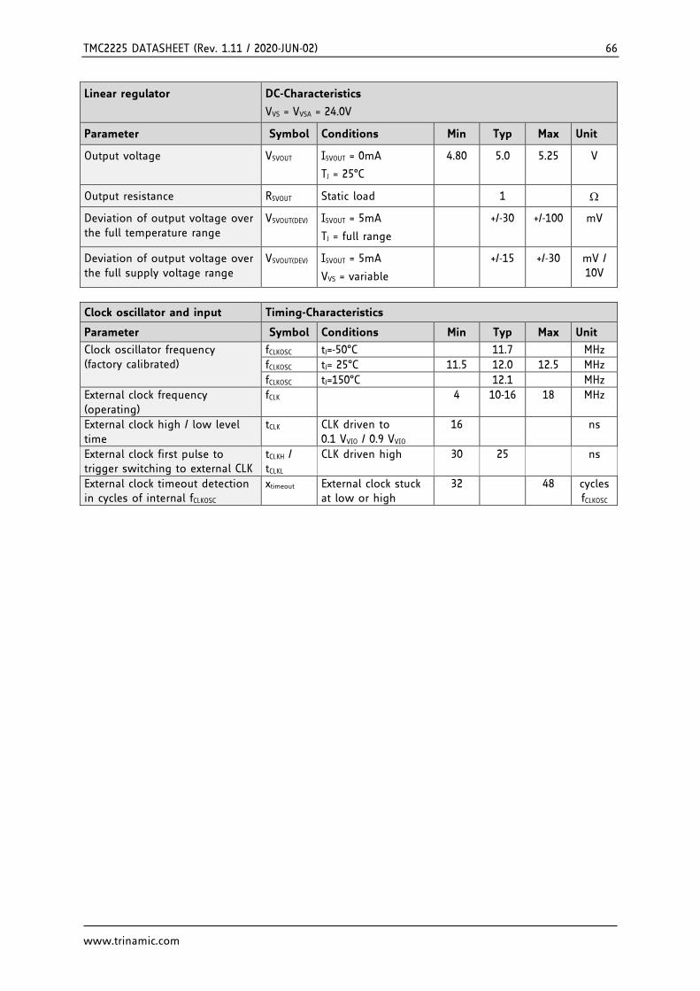
TMC2225 DATASHEET (Rev. 1.11 / 2020-JUN-02) 66
www.trinamic.com
Linear regulator DC-Characteristics
VVS = VVSA = 24.0V
Parameter Symbol Conditions Min Typ Max Unit
Output voltage V5VOUT I5VOUT = 0mA
TJ = 25°C
4.80 5.0 5.25 V
Output resistance R5VOUT Static load 1
Deviation of output voltage over the full temperature range
V5VOUT(DEV) I5VOUT = 5mA
TJ = full range
+/-30 +/-100 mV
Deviation of output voltage over the full supply voltage range
V5VOUT(DEV) I5VOUT = 5mA
VVS = variable
+/-15 +/-30 mV / 10V
Clock oscillator and input Timing-Characteristics
Parameter Symbol Conditions Min Typ Max Unit
Clock oscillator frequency (factory calibrated)
fCLKOSC tJ=-50°C 11.7 MHz
fCLKOSC tJ= 25°C 11.5 12.0 12.5 MHz
fCLKOSC tJ=150°C 12.1 MHz
External clock frequency (operating)
fCLK 4 10-16 18 MHz
External clock high / low level time
tCLK CLK driven to 0.1 VVIO / 0.9 VVIO
16 ns
External clock first pulse to trigger switching to external CLK
tCLKH / tCLKL
CLK driven high 30 25 ns
External clock timeout detection in cycles of internal fCLKOSC
xtimeout External clock stuck at low or high
32 48 cycles fCLKOSC

TMC2225 DATASHEET (Rev. 1.11 / 2020-JUN-02) 67
www.trinamic.com
Detector levels DC-Characteristics
Parameter Symbol Conditions Min Typ Max Unit
VVS undervoltage threshold for RESET
VUV_VS VVS rising 3.5 4.2 4.6 V
V5VOUT undervoltage threshold for RESET
VUV_5VOUT V5VOUT rising 3.5 V
VVCC_IO undervoltage threshold for RESET
VUV_VIO VVCC_IO rising (delay typ. 10µs)
2.1 2.55 3.0 V
VVCC_IO undervoltage detector hysteresis
VUV_VIOHYST 0.3 V
Short to GND detector threshold (VVS - VOx)
VOS2G 2 2.5 3 V
Short to VS detector threshold (VOx)
VOS2VS 1.6 2 2.3 V
Short detector delay (high side / low side switch on to short detected)
tS2G High side output clamped to VSP-3V
0.8 1.3 2 µs
Overtemperature prewarning 120°C
tOTPW Temperature rising 100 120 140 °C
Overtemperature shutdown or prewarning 143°C (appr. 153°C IC peak temp.)
tOT143 Temperature rising 128 143 163 °C
Overtemperature shutdown 150°C (appr. 160°C IC peak temp.)
tOT150 Temperature rising 135 150 170 °C
Overtemperature shutdown 157°C (appr. 167°C IC peak temp.)
tOT157 Temperature rising 142 157 177 °C
Difference between temperature detector and power stage temperature, slow heat up
tOTDIFF Power stage causing high temperature, normal 4 Layer PCB
10 °C
Sense resistor voltage levels DC-Characteristics
fCLK=16MHz
Parameter Symbol Conditions Min Typ Max Unit
Sense input peak threshold voltage (low sensitivity)
VSRTL vsense=0 csactual=31 CUR_A/B=248 Hyst.=0; IBRxy=0
325 mV
Sense input peak threshold voltage (high sensitivity)
VSRTH vsense=1 csactual=31 CUR_A/B=248 Hyst.=0; IBRxy=0
180 mV
Sense input tolerance / motor current full scale tolerance -using internal reference
ICOIL I_scale_analog=0, vsense=0
-5 +5 %
Sense input tolerance / motor current full scale tolerance -using external reference voltage
ICOIL I_scale_analog=1, VAIN=2V, vsense=0
-2 +2 %
Internal resistance from pin BRxy to internal sense comparator (additional to sense resistor)
RBRxy 30 mΩ

TMC2225 DATASHEET (Rev. 1.11 / 2020-JUN-02) 68
www.trinamic.com
Digital pins DC-Characteristics
Parameter Symbol Conditions Min Typ Max Unit
Input voltage low level VINLO -0.3 0.3 VVIO V
Input voltage high level VINHI 0.7 VVIO VVIO+0.3 V
Input Schmitt trigger hysteresis VINHYST 0.12 VVIO
V
Output voltage low level VOUTLO IOUTLO = 2mA 0.2 V
Output voltage high level VOUTHI IOUTHI = -2mA VVIO-0.2 V
Input leakage current IILEAK -10 10 µA
Pullup / pull-down resistors RPU/RPD 132 166 200 kΩ
Digital pin capacitance C 3.5 pF
AIN/IREF input DC-Characteristics
Parameter Symbol Conditions Min Typ Max Unit
AIN_IREF input resistance to 2.5V (=5VOUT/2)
RAIN Measured to GND (internalRsense=0)
260 330 400 kΩ
AIN_IREF input voltage range for linear current scaling
VAIN Measured to GND (IscaleAnalog=1)
0 0.5-2.4 V5VOUT/2 V
AIN_IREF open input voltage level
VAINO Open circuit voltage
(internalRsense=0)
V5VOUT/2 V
AIN_IREF input resistance to GND for reference current input
RIREF Measured to GND (internalRsense=1)
0.5 0.7 1.0 kΩ
AIN_IREF current amplification for reference current to coil current at maximum setting
IREFAMPL IIREF = 0.25mA 3000 Times
Motor current full scale tolerance -using RDSon measurement (value for design guideline to calculate reproduction of certain motor current & torque)
ICOIL Internal_Rsense=1, vsense=0, IIREF = 0.25mA (after reaching thermal balance)
-10 +10 %

TMC2225 DATASHEET (Rev. 1.11 / 2020-JUN-02) 69
www.trinamic.com
18.3 Thermal Characteristics The following table shall give an idea on the thermal resistance of the package. The thermal resistance for a four-layer board will provide a good idea on a typical application. Actual thermal characteristics will depend on the PCB layout, PCB type and PCB size. The thermal resistance will benefit from thicker CU (inner) layers for spreading heat horizontally within the PCB. Also, air flow will reduce thermal resistance. A thermal resistance of 26K/W for a typical board means, that the package is capable of continuously dissipating 3.8W at an ambient temperature of 25°C with the die temperature staying below 125°C. Note, that a thermally optimized layout is required.
Parameter Symbol Conditions Typ Unit
Typical power dissipation PD StealthChop or SpreadCycle, 1A RMS in two phase motor, sinewave, 40 or 20kHz chopper, 24V, 110°C peak surface of package (motor QSH4218-035-10-027)
2.5 W
Typical power dissipation PD StealthChop or SpreadCycle, 0.7A RMS in two phase motor, sinewave, 40 or 20kHz chopper, 24V, 68°C peak surface of package (motor QSH4218-035-10-027)
1.36 W
Thermal resistance junction to ambient on a multilayer board
HTSSOP28
RTMJA Dual signal and two internal power plane board (2s2p) as defined in JEDEC EIA JESD51-5 and JESD51-7 (FR4, 35µm CU, 70mm x 133mm, d=1.5mm)
26 K/W
Thermal resistance junction to case
RTJC Junction to heat slug of package 6 K/W
Table 18.1 Thermal characteristics TMC2225
Note A spread-sheet for calculating TMC2225 power dissipation is available on www.trinamic.com.
TMC2225 DATASHEET (Rev. 1.11 / 2020-JUN-02) 70
www.trinamic.com
19 Layout Considerations
19.1 Exposed Die Pad The TMC2225 uses its die attach pad to dissipate heat from the drivers and the linear regulator to the board. For best electrical and thermal performance, use a reasonable amount of solid, thermally conducting vias between the die attach pad and the ground plane. The printed circuit board should have a solid ground plane spreading heat into the board and providing for a stable GND reference.
19.2 Wiring GND All signals of the TMC2225 are referenced to their respective GND. Directly connect all GND pins under the device to a common ground area (GND and die attach pad). The GND plane right below the die attach pad should be treated as a virtual star point. For thermal reasons, the PCB top layer shall be connected to a large PCB GND plane spreading heat within the PCB.
Attention Especially the sense resistors are susceptible to GND differences and GND ripple voltage, as the microstep current steps make up for voltages down to 0.5 mV. No current other than the sense resistor current should flow on their connections to GND and to the TMC2225. Optimally place them close to the IC, with one or more vias to the GND plane for each sense resistor. The two sense resistors for one coil should not share a common ground connection trace or vias, as also PCB traces have a certain resistance.
19.3 Supply Filtering The 5VOUT output voltage ceramic filtering capacitor (2.2 to 4.7 µF recommended) should be placed as close as possible to the 5VOUT pin, with its GND return going directly to the die pad or the nearest GND pin. This ground connection shall not be shared with other loads or additional vias to the GND plane. Use as short and as thick connections as possible. The motor supply pins VS should be decoupled with an electrolytic capacitor (47 μF or larger is recommended) and a ceramic capacitor, placed close to the device. Take into account that the switching motor coil outputs have a high dV/dt. Thus, capacitive stray into high resistive signals can occur, if the motor traces are near other traces over longer distances.

TMC2225 DATASHEET (Rev. 1.11 / 2020-JUN-02) 71
www.trinamic.com
19.4 Layout Example TMC2225 Schematic
Placement (Excerpt) Top Layout (Excerpt, showing die pad vias)
The complete schematics and layout data for all TMC2225 evaluation boards are available on the TRINAMIC website.

TMC2225 DATASHEET (Rev. 1.11 / 2020-JUN-02) 72
www.trinamic.com
20 Package Mechanical Data
20.1 Dimensional Drawings HTSSOP28
Figure 20.1 Dimensional drawings HTSSOP28

TMC2225 DATASHEET (Rev. 1.11 / 2020-JUN-02) 73
www.trinamic.com
Parameter [mm] Ref Min Nom Max
total thickness A 1.2
stand off A1 0.05 0.15
mold thickness A2 0.90 1.00 1.10
mold thickness over LF A3 0.34 0.44 0.54
lead width b 0.2 0.29
width w/o plating b1 0.19 0.22 0.25
(optional plating) b2 0.19 0.25
lead frame thickness c 0.13 0.18
thickness w/o plating c1 0.12 0.13 0.14
(optional plating) c2 0.12 0.14
body size X D 9.60 9.70 9.80
exposed die pad size Y D1 6.20REF
width over pins E 6.20 6.40 6.60
body size Y E1 4.30 4.40 4.50
exposed die pad size X E2 2.75REF
lead pitch e 0.55 0.65 0.75
lead L 0.45 0.60 0.75
lead length L1 1.00REF
L2 0.25BSC
R 0.09
R1 0.09
lead stand off S 0.20
0° 8°
1 10° 12° 14°
2 10° 12° 14°
3 10° 12° 14°
20.2 Package Codes
Type Package Temperature range Code & marking
TMC2225-SA HTSSOP28 (RoHS) -40°C ... +125°C TMC2225-SA
TMC… -T -T suffix denotes tape on reel packed products
TMC2225 DATASHEET (Rev. 1.11 / 2020-JUN-02) 74
www.trinamic.com
21 Table of Figures FIGURE 1.1 TMC2225 BASIC APPLICATION BLOCK DIAGRAM ...................................................................................................... 4 FIGURE 1.2 STAND-ALONE DRIVER WITH PRE-CONFIGURATION .................................................................................................... 5 FIGURE 1.3 AUTOMATIC MOTOR CURRENT POWER DOWN .......................................................................................................... 7 FIGURE 2.1 TMC2225 PINNING TOP VIEW – TYPE: HTSSOP28, 9.7X6.4MM² OVER PINS, 0.65MM PITCH ............................... 8 FIGURE 3.1 STANDARD APPLICATION CIRCUIT ........................................................................................................................... 10 FIGURE 3.2 APPLICATION CIRCUIT USING RDSON BASED SENSING ........................................................................................... 11 FIGURE 3.3 5V ONLY OPERATION .............................................................................................................................................. 11 FIGURE 3.4 SIMPLE ESD ENHANCEMENT AND MORE ELABORATE MOTOR OUTPUT PROTECTION .................................................. 13 FIGURE 4.1 ATTACHING THE TMC2225 TO A MICROCONTROLLER UART .................................................................................. 16 FIGURE 4.2 ADDRESSING MULTIPLE TMC2225 VIA SINGLE WIRE INTERFACE USING ANALOG SWITCHES .................................. 17 FIGURE 6.1 MOTOR COIL SINE WAVE CURRENT WITH STEALTHCHOP (MEASURED WITH CURRENT PROBE) .................................. 32 FIGURE 6.2 STEALTHCHOP2 AUTOMATIC TUNING PROCEDURE ................................................................................................... 34 FIGURE 6.3 SCOPE SHOT: GOOD SETTING FOR PWM_REG ....................................................................................................... 36 FIGURE 6.4 SCOPE SHOT: TOO SMALL SETTING FOR PWM_REG DURING AT#2 ....................................................................... 36 FIGURE 6.5 SUCCESSFULLY DETERMINED PWM_GRAD(_AUTO) AND PWM_OFS(_AUTO) ................................................... 36 FIGURE 6.6 VELOCITY BASED PWM SCALING (PWM_AUTOSCALE=0) ......................................................................................... 38 FIGURE 6.7 TPWMTHRS FOR OPTIONAL SWITCHING TO SPREADCYCLE ................................................................................... 39 FIGURE 7.1 CHOPPER PHASES ................................................................................................................................................... 43 FIGURE 7.2 NO LEDGES IN CURRENT WAVE WITH SUFFICIENT HYSTERESIS (MAGENTA: CURRENT A, YELLOW & BLUE: SENSE
RESISTOR VOLTAGES A AND B) ......................................................................................................................................... 45 FIGURE 7.3 SPREADCYCLE CHOPPER SCHEME SHOWING COIL CURRENT DURING A CHOPPER CYCLE ............................................ 46 FIGURE 9.1 SCALING THE MOTOR CURRENT USING THE ANALOG INPUT...................................................................................... 50 FIGURE 11.1 STEP AND DIR TIMING, INPUT PIN FILTER ......................................................................................................... 53 FIGURE 11.2 MICROPLYER MICROSTEP INTERPOLATION WITH RISING STEP FREQUENCY (EXAMPLE: 16 TO 256) ..................... 55 FIGURE 11.3 INDEX SIGNAL AT POSITIVE ZERO TRANSITION OF THE COIL A SINE CURVE .......................................................... 56 FIGURE 12.1 SOFTWARE GENERATED MOTION PROFILE ............................................................................................................. 57 FIGURE 13.1 DIAG AND INDEX OUTPUTS ............................................................................................................................... 59 FIGURE 14.1 CURRENT SETTING AND FIRST STEPS WITH STEALTHCHOP .................................................................................... 60 FIGURE 14.2 TUNING STEALTHCHOP AND SPREADCYCLE .......................................................................................................... 61 FIGURE 14.3 OTP PROGRAMMING ............................................................................................................................................ 62 FIGURE 20.1 DIMENSIONAL DRAWINGS HTSSOP28 ................................................................................................................ 72

TMC2225 DATASHEET (Rev. 1.11 / 2020-JUN-02) 75
www.trinamic.com
22 Revision History
Version Date Author BD= Bernhard Dwersteg
Description
V1.09 2019-Jul-25 BD Added dimensioning for HTSSOP package First version of dedicated TMC2225 datasheet
V1.10 2019-Sep-13 BD Corrected TMC2225 package code and type in table
V1.11 2020-Jun-02 BD Minor corrections, Logo
Table 22.1 Document Revisions
23 References [TMC2225-EVAL] TMC2225 Evaluation board: Manuals, software and PCB data available on
www.trinamic.com [AN001] Trinamic Application Note 001 - Parameterization of SpreadCycle™,
www.trinamic.com
Calculation sheet TMC2225_Calculations.xlsx www.trinamic.com