
Time-Resolved Photoemission Electron Microscopy ...
125
Time-Resolved Photoemission Electron Microscopy: Development and Applications Wittenbecher, Lukas 2021 Document Version: Publisher's PDF, also known as Version of record Link to publication Citation for published version (APA): Wittenbecher, L. (2021). Time-Resolved Photoemission Electron Microscopy: Development and Applications. Lund University , Department of physics. Total number of authors: 1 General rights Unless other specific re-use rights are stated the following general rights apply: Copyright and moral rights for the publications made accessible in the public portal are retained by the authors and/or other copyright owners and it is a condition of accessing publications that users recognise and abide by the legal requirements associated with these rights. • Users may download and print one copy of any publication from the public portal for the purpose of private study or research. • You may not further distribute the material or use it for any profit-making activity or commercial gain • You may freely distribute the URL identifying the publication in the public portal Read more about Creative commons licenses: https://creativecommons.org/licenses/ Take down policy If you believe that this document breaches copyright please contact us providing details, and we will remove access to the work immediately and investigate your claim. Download date: 26. Jan. 2022
Transcript of Time-Resolved Photoemission Electron Microscopy ...
LUND UNIVERSITY
PO Box 117221 00 Lund+46 46-222 00 00
Time-Resolved Photoemission Electron Microscopy: Development and Applications
Wittenbecher, Lukas
2021
Document Version:Publisher's PDF, also known as Version of record
Link to publication
Citation for published version (APA):Wittenbecher, L. (2021). Time-Resolved Photoemission Electron Microscopy: Development and Applications.Lund University , Department of physics.
Total number of authors:1
General rightsUnless other specific re-use rights are stated the following general rights apply:Copyright and moral rights for the publications made accessible in the public portal are retained by the authorsand/or other copyright owners and it is a condition of accessing publications that users recognise and abide by thelegal requirements associated with these rights. • Users may download and print one copy of any publication from the public portal for the purpose of private studyor research. • You may not further distribute the material or use it for any profit-making activity or commercial gain • You may freely distribute the URL identifying the publication in the public portal
Read more about Creative commons licenses: https://creativecommons.org/licenses/Take down policyIf you believe that this document breaches copyright please contact us providing details, and we will removeaccess to the work immediately and investigate your claim.
Download date: 26. Jan. 2022
Time-Resolved Photoemission Electron Microscopy: Development and ApplicationsLUKAS WITTENBECHER
DEPARTMENT OF PHYSICS | FACULTY OF SCIENCE | LUND UNIVERSITY

ISBN 978-91-7895-977-8
Division of Synchrotron Radiation ResearchDepartment of Physics
Faculty of ScienceLund University 9
789178
959778
NO
RDIC
SW
AN
EC
OLA
BEL
3041
090
3Pr
inte
d by
Med
ia-T
ryck
, Lun
d 20
21
Time-Resolved Photoemission Electron Microscopy: Development
and Applications
Lukas Wittenbecher
DOCTORAL DISSERTATION
by due permission of the Faculty of Science, Lund University, Sweden. To be defended in the Rydberg Lecture Hall at the Department of Physics on
Thursday, the 7th of October 2021 at 9:15.
Faculty opponent Professor Tobias Brixner, Universität Würzburg

Organization LUND UNIVERSITY
Division of Synchrotron Radiation Research
Document name Doctoral thesis
Department of Physics, Box 118 S-22100 Lund
Date of issue 2021-10-07
Author: Lukas Wittenbecher
Sponsoring organization
Title and subtitle Time-Resolved Photoemission Electron Microscopy: Development and Applications Abstract Time-resolved photoemission electron microscopy (TR-PEEM) belongs to a class of experimental techniques combining the spatial resolution of electron-based microscopy with the time resolution of ultrafast optical spectroscopy. This combination provides insight into fundamental processes on the nanometer spatial and femto/picosecond time scale, such as charge carrier transport in semiconductors or collective excitations of conduction band electrons at metal surfaces. The high spatiotemporal resolution also offers a detailed view of the relationship between local structure and ultrafast photoexcitation dynamics in nanostructures and nanostructured materials, which is beneficial in exploring new materials and applications in opto-electronics and nano-optics.
This thesis describes the investigation of ultrafast photoexcitation dynamics in metal- and III-V semiconductor nanostructures using TR-PEEM. We investigate hot carrier cooling in individual InAs nanowires where we find evidence that electron-hole scattering strongly contributes to the intra-band energy relaxation of photoexcited electrons on a sub-picosecond time scale and we observe ultrafast hot electron transport towards the nanowire surface due to an in-built electric field. We demonstrate the combination of TR-PEEM with optical time-domain spectroscopy to enable time- and excitation frequency-resolved PEEM imaging. The technique is applied to GaAs substrates and nanowires. TR-PEEM is further used to investigate localized and propagating surface plasmon polaritons. We explore the optical properties of disordered, porous gold nano-particles (nanosponges). Using TR-PEEM, we can resolve several plasmonic hotspots with different resonance frequencies and lifetimes within single nanosponges. We also explore excitation and temporal control of surface plasmon polaritons by means of single-layered crystals of the transition metal dichalcogenide WSe2.
In addition, this thesis includes developments in ultrafast optics, aiming to expand the capabilities of the TR-PEEM setup. We present a setup for generating tunable broadband ultraviolet (UV) laser pulses via achromatic second harmonic generation. The setup is suitable for operation at high repetition rates and low pulse energies due to its high conversion efficiency. Further, we describe a transmission grating-based interferometer for the generation of stable, phase-locked pulse pairs. Pulse shaping based on liquid crystal technology allows accurate control over the temporal shape of femtosecond laser pulses. We characterize Fabry-Perot interferences affecting the accuracy of such pulse shapers, and we demonstrate a calibration scheme to compensate for these interference effects.
Key words PEEM, time-resolved PEEM, ultrafast optics, pulse shaping, plasmonics, semiconductor nanowires, hot electrons, ultrafast microscopy, charge carrier relaxation Classification system and/or index terms (if any)
Supplementary bibliographical information Language English
ISSN and key title ISBN 978-91-7895-977-8 (print) 978-91-7895-978-5 (pdf)
Recipient’s notes Number of pages 306 Price
Security classification
I, the undersigned, being the copyright owner of the abstract of the above-mentioned dissertation, hereby grant to all reference sources permission to publish and disseminate the abstract of the above-mentioned dissertation.
Signature Date 2021-08-27
Time-Resolved Photoemission Electron Microscopy: Development
and Applications
Lukas Wittenbecher

Cover photo:
Photo of a PEEM sample under laser illumination, placed in the experimental chamber in front of the microscope’s extractor cone.
Pages i to 106 © Lukas Wittenbecher
Paper I © 2021 Optical Society of America under the OSA Open Access Publishing Agreement.
Paper II © 2020 Optical Society of America under the OSA Open Access Publishing Agreement.
Paper III © 2019 Optical Society of America under the OSA Open Access Publishing Agreement.
Paper IV © 2021 The Authors, licensed under CC-BY 4.0. Published by American Chemical Society.
Paper V © 2021 The Authors.
Paper VI © 2020 The authors, licensed under CC-BY 4.0. Published by Nature Publishing Group.
Paper VII © 2021 The authors, licensed under CC-BY 4.0. Published by American Chemical Society.
Division of Synchrotron Radiation Research Department of Physics, Faculty of Science Lund University
ISBN 978-91-7895-977-8 (print)978-91-7895-978-5 (pdf)
Printed in Sweden by Media-Tryck, Lund University Lund 2021
i
Table of Contents
List of Publications ............................................................................................... iii
Popular Science Summary ...................................................................................... vi
Abbreviations and Symbols ................................................................................. viii
1 Introduction ................................................................................................ 1 1.1 Scope of this work ................................................................................. 3 1.2 Outline .................................................................................................. 4
2 Elements of Ultrafast Optics ........................................................................ 5 2.1 Femtosecond Laser pulses ...................................................................... 6
2.1.1 Basic description of laser pulses .................................................. 6 2.1.2 Dispersion and dispersion control ............................................ 10
2.2 Fourier Transform Pulse Shaping ......................................................... 12 2.2.1 Liquid crystal spatial light modulators ...................................... 14
2.3 Nonlinear optics .................................................................................. 16 2.3.1 Phase-matching ........................................................................ 18 2.3.2 Optical parametric amplification .............................................. 20
3 Light-Matter Interaction at the Nanoscale.................................................. 23 3.1 III-V compound semiconductors ......................................................... 23
3.1.1 III-V semiconductor nanowires ................................................ 26 3.2 Photoexcited electrons in semiconductors ............................................ 29
3.2.1 Carrier relaxation ..................................................................... 29 3.2.2 Electron transport .................................................................... 34
3.3 Surface plasmon polaritons .................................................................. 37 3.3.1 The dielectric function of noble metals .................................... 38 3.3.2 Surface plasmon polaritons at metal-dielectric interfaces .......... 40 3.3.3 Localized plasmons polaritons .................................................. 42
4 Photoemission ........................................................................................... 45 4.1 Direct photoemission ........................................................................... 45
ii
4.2 Perturbative multiphoton photoemission ............................................. 48 4.3 Other electron emission processes ........................................................ 49
4.3.1 Strong-field photoemission ...................................................... 49 4.3.2 Thermionic emission ............................................................... 49 4.3.3 Secondary electron emission ..................................................... 50
5 Time-Resolved Photoemission Electron Microscopy .................................. 51 5.1 Principle of PEEM ............................................................................... 51
5.1.1 Contrast mechanisms ............................................................... 52 5.1.2 Spatial resolution ..................................................................... 54 5.1.3 Surface sensitivity ..................................................................... 56
5.2 Time-resolved PEEM .......................................................................... 57 5.2.1 Pump-probe PEEM ................................................................. 58 5.2.2 Interferometric time-resolved PEEM ....................................... 62 5.2.3 Space charge effects .................................................................. 65
6 Summary of Results ................................................................................... 67 6.1 Developments in Ultrafast Optics ........................................................ 67
6.1.1 Generation of UV pulses via achromatic phase-matching ......... 69 6.1.2 Grating-based interferometer ................................................... 72 6.1.3 Correction of Fabry-Perot interferences in liquid crystal spatial light modulators ................................................................................... 74
6.2 PEEM applications .............................................................................. 76 6.2.1 Hot electron relaxation in InAs nanowires ............................... 76 6.2.2 Excitation frequency resolved PEEM ....................................... 79 6.2.3 Plasmonic hotspots in gold nanosponges .................................. 82 6.2.4 Excitation and control of SPPs using 2D transition metal dichalcogenides ..................................................................................... 83
7 Concluding Remarks and Outlook ............................................................. 87
References ............................................................................................................ 91
Acknowledgements ............................................................................................ 107
iii
List of Publications
This doctoral thesis is based on the following papers, which will be referred to in the text by their Roman numerals.
I Generation and compression of 10-fs deep ultraviolet pulses at high repetition rate using standard optics L. Bruder, L. Wittenbecher, P. Kolesnichenko, D. Zigmantas. Opt. Express 2021, 29 (16), 25593.
I was involved in the construction of the experimental setup, and I took part in the experiments. I performed and analyzed the ray tracing calculations, and I took part in writing and discussing the manuscript.
II Fully Symmetric Dispersionless Stable Transmission-Grating Michelson Interferometer P. Kolesnichenko, L. Wittenbecher, D. Zigmantas. Opt. Express 2020, 28 (25), 37752.
I participated in the experiments, performed, and analyzed the ray tracing calculations and I took part in writing and discussing the manuscript.
III Correction of Fabry-Pérot Interference Effects in Phase and Amplitude Pulse Shapers Based on Liquid Crystal Spatial Light Modulators L. Wittenbecher, D. Zigmantas. Opt. Express 2019, 27 (16), 22970.
I constructed the experimental setup, planned, and carried out the experiments. I analyzed the data and wrote the manuscript.
iv
IV Unraveling the Ultrafast Hot Electron Dynamics in Semiconductor Nanowires L. Wittenbecher, E. Viñas Boström, J. Vogelsang, S. Lehman, K. A. Dick, C.Verdozzi, D. Zigmantas, A. Mikkelsen.ACS Nano 2021, 15 (1), 1133–1144
I assembled the experimental setup, planned and carried out the experiments. I analyzed the data and wrote the manuscript.
V Excitation frequency-resolved ultrafast photoemission electron microscopy for imaging of carrier dynamics at semiconductor surfaces L. Wittenbecher, P. Kolesnichenko, S. Lehmann, A. Mikkelsen, D.Zigmantas. In manuscript
I was involved in planning the experiments and I was the main responsible for carrying out the measurements. I analyzed the data and wrote the manuscript.
VI Nonlinear Plasmon-Exciton Coupling Enhances Sum-Frequency Generation from a Hybrid Metal/Semiconductor Nanostructure J. H. Zhong, J. Vogelsang, J. M. Yi, D. Wang, L. Wittenbecher, S. Mikaelsson, A. Korte, A. Chimeh, C. L. Arnold, P. Schaaf, E. Runge, A. L’Huillier, A. Mikkelsen, C. Lienau. Nat. Commun. 2020, 11 (1), 1–10.
I participated in the time-resolved PEEM experiments, and I contributed to the discussion of the manuscript.
VII Coherent Excitation and Control of Plasmons on Gold Using Two-Dimensional Transition Metal Dichalcogenides J. Vogelsang, L. Wittenbecher, D. Pan, J. Sun, S. Mikaelsson, C. L. Arnold, A.L’Huillier, H. Xu, A. Mikkelsen.ACS Photonics 2021, 8 (6), 1607–1615.
I participated in the experiments, and I contributed to the discussion of the manuscript.

v
Publications not included in this thesis:
VIII Understanding Radiative Transitions and Relaxation Pathways in Plexcitons D. Finkelstein-Shapiro, P. A. Mante, S. Sarisozen, L. Wittenbecher, I. Minda, S. Balci, T. Pullerits, D. Zigmantas. Chem 2021, 7 (4), 1092–1107.
vi
Popular Science Summary
Throughout the last decades, we have become better and better at creating and manipulating structures at the nanometer scale (one nanometer is a billionth of a meter). One motivation for this is miniaturization: Transistors, which are the basic building blocks of our computers and mobile phones, are today only few tens of nanometers in size, making it possible to integrate many billions of them in computer chips as small as your fingertip.
Another reason for the immense interest in nanostructures is that the behavior of many materials changes dramatically when their size approaches the nanoscale. In the research field of nano-photonics, scientists make use of this phenomenon to create nanoscale structures that interact with light in a specific way. For example, nanometer-sized semiconductor needles (‘nanowires’) can be designed to show enhanced absorption of light, useful for converting sunlight into electric power in a solar cell. Another example are nanoparticles made of gold or silver, which can be designed to focus light into tiny spots. This might, among other things, lead to sensors able to detect single molecules or to less invasive treatments for cancer.
In this thesis, we have studied the processes unfolding within single nanostructures when interacting with light. This is challenging for two reasons:
First, nanostructures are, by definition, very small. So small, in fact, that conventional light microscopes can at best produce blurry images of single nanostructures in which much of the interesting information is hidden. This is a consequence of the so-called optical diffraction limit, which fundamentally restricts the resolution of optical microscopes. One way to circumvent this limitation is the use of electron microscopy, where electrons are used instead of light to form an image. In this thesis, we used a photoemission electron microscope, or PEEM in short, which creates high-resolution images of nanostructures using electrons released from their surface.
The second challenge is that many processes triggered by light take place on an incredibly short time scale, sometimes within only a few femtoseconds (10-15 seconds). It is hard to comprehend how short one femtosecond really is because this unit of time is so utterly detached from our everyday experience. I will try to illustrate this by embarking on an imaginary journey through time:
vii
We are traveling back in time to the beginning of the Oligocene epoch about 34 million years ago. The Himalayas have begun to slowly rise from the ocean, and early ancestors of mammals we know today are roaming the landscape. Another 26 to 30 million years will pass until a new branch in the evolution of apes emerges, leading eventually to the appearance of the homo sapiens. Civilizations will rise and fall. The alphabet, the printing press, and modern technology will be invented, allowing me to type these words on my computer on a Saturday in late August in 2021. During all this time, about 1015seconds have passed. Likewise, 1015 femtoseconds make up one second.
Not even the most advanced electronics available today are fast enough to follow events on the femtosecond time scale. Instead, researchers use short pulses of laser light. Often, these pulses are used in so-called pump-probe experiments, where a first laser pulse (the pump) triggers a process in the sample before a second laser pulse (the probe) is used to take a snapshot, much like the flash of a camera. By taking snapshots at different times, a slow-motion movie of the whole process can be assembled.
In this thesis, we have carried out such pump-probe experiments inside an electron microscope. That way, we could combine the best of both worlds and record sharp images of nanostructures with femtosecond time resolution. We have studied a variety of nanoparticles, from ‘nanowires’ to ‘nanosponges’ (small, porous particles). Some of our studies have focused on relaxation processes: light interacting with nanostructures transfers part of its energy to the electrons in the material. We tried to understand how fast, and through which mechanisms, the electrons lose this energy again. In other cases, we have investigated how light itself can be concentrated and manipulated on the nanoscale. Our results contribute to the collective effort of understanding the interaction between light and matter at the nanoscale and might – one day – contribute to the development of new nano-technologies.

viii
Abbreviations and Symbols
2D Two-dimensionalAPM Achromatic phase-matchingBBO 𝛽 barium borate CB Conduction bandCCD Charge coupled device DFG Difference-frequency generationFWHM Full width at half maximum IS-PEEM Integral sample stage photoemission electron microscope ITR-PEEM Interferometric time-resolved photoemission electron microscopy LC Liquid crystalLC-SLM Liquid crystal spatial light modulator LED Light emitting diode LEED Low energy electron diffraction LEEM Low energy electron microscopy LO Longitudinal optical LSP Localized surface plasmon MBE Molecular beam epitaxy MOVPE Metal-organic vapor phase epitaxy NIR Near-infraredNOPA Non-collinear optical parametric amplification/amplifier OPA Optical parametric amplification/amplifier PE PhotoemissionPEEM Photoemission electron microscopy/microscope SCR Space charge regionSEM Scanning electron microscope SFG Sum-frequency generationSHG Second harmonic generation SPP Surface plasmon polariton TR-PEEM Time-resolved photoemission electron microscopy UV UltravioletVB Valence band

ix
VIS Visible WZ Wurtzite XUV Extreme ultraviolet ZB Zincblende 𝑐 Speed of light in vacuum e-/h+ Electron/hole 𝐸 Fermi level 𝐸 Bandgap 𝐸 Vacuum level ℏ𝜔 Photon energy Δ𝑡, Δ𝑇 Time delay 𝜒 Electron affinity 𝑊 Work function


1
1 Introduction
Scientists across disciplines have always been striving to expand their experimental capacities, whether to find elusive particles, record the echo of distant cosmic events, resolve smaller and smaller structures, or monitor some of the fastest processes occurring in nature. A case in point is the field of microscopy – from the ancient Greek words mikrós (small) and skopeĩn (to observe) – which has undergone an astonishing development since the early 20th century. Conventional optical microscopes cannot resolve features smaller than roughly half the optical wavelength due to the diffraction of light, limiting the spatial resolution to a few hundred nanometers. To overcome this limitation, researchers resorted to imaging with electrons, which – just like light – can behave as waves but have substantially shorter wavelengths, pushing the fundamental limit on resolution into the picometer range. As electron optics have become more sophisticated, the resolution of electron microscopes has continuously improved. Today, transmission electron microscopes can resolve the arrangement of atoms in materials with Ångström resolution1, rivaled only by scanning probe microscopy techniques which can also produce spectacular images of the (atomic) structure of surfaces and molecules with comparable resolution2,3.
In a parallel development initiated by the realization of the first laser in 19604, spectroscopists and laser physicists began to explore light-induced dynamic processes unfolding within picoseconds or faster, such as energy transfer through the photosynthetic apparatus5 or the relaxation of excited electrons in solids6. In monitoring dynamics on this time scale (often referred to as ultrafast dynamics), the coherent nature of light emitted by lasers plays a critical role: it enables the creation of laser pulses as short as a few femtoseconds by ‘locking’ laser modes of different frequency in phase7. In a typical time-resolved experiment, a first laser pulse (‘pump’) repeatedly pushes the sample out of equilibrium. In each such cycle, a delayed second pulse probes the system's current state, much like a short flash of light in stroboscopic imaging. By repeating this process for different time delays between the pulses, it is possible to follow ultrafast processes directly in the time domain. Such pump-probe measurements are nowadays routinely carried out, and they have contributed
2
immensely to our current understanding of ultrafast processes in, e.g., solids, molecules, and biological systems.
Both developments described above at first proceeded independently. However, as advances in microscopy and laser technology made the instruments more reliable and accessible, researchers began to combine electron-based imaging with approaches from optical time-resolved spectroscopy1,8–10, capitalizing on the strengths of each method to accomplish nanoscale imaging with femtosecond time resolution. This combination offers many intriguing possibilities: First, to study fundamental processes directly on their natural time and length scales, such as the collective excitation of surface electrons in metals (surface plasmon polaritons) or transport of photoexcited electrons in semiconductors. Second, the possibility to gain new insights into the relationship between local structure and excitation dynamics in spatially heterogeneous materials, exploring, for instance, the effect of grain boundaries11 or local morphology on nanostructured surfaces12. Lastly, we consider the context of nanoscience, where size-effects emerging on the nanoscale are often exploited to design nanostructures with new physical properties compared to bulk materials. Here, the ability to spatially resolve ultrafast dynamics is especially valuable. It allows the characterization of dynamics within single nanostructures, illuminating the interplay between several components in heterostructures and providing statistical information not accessible in ensemble-averaged methods.
The exploration of ultrafast phenomena on the nanometer scale is not merely of academic interest. Several essential technologies, such as laser diodes, solar cells, light detectors, and fiber-optic communication, rely on the interaction between light and matter. And while many such devices operate in a steady-state regime, electrons excited by light may still undergo various ultrafast relaxation processes which can severely affect the overall device efficiency, such as intraband relaxation and trapping in solar cell materials. Conversely, numerous proposals for new technologies suggest specifically exploiting or manipulating ultrafast photoexcitation processes to construct new types of devices with increased efficiency or new functionality13–15. A detailed characterization of the spatiotemporal photoexcitation dynamics is a substantial benefit in developing new materials and devices.
One technique that combines the spatial resolution of electron-based imaging with the femtosecond time resolution of laser-based spectroscopy is time-resolved photoemission electron microscopy (TR-PEEM) – the subject of this thesis. This microscopy technique relies on photoelectrons emitted from the sample upon optical excitation to form a high-resolution image of the sample surface. PEEM instruments for ‘conventional’ imaging are typically operated with table-top UV sources such as Hg or He lamps or at synchrotron facilities. However, when these light sources are

3
replaced by femtosecond laser pulses, sample excitation and the generation of photoelectrons can be timed with femtosecond precision, enabling time-resolved imaging of ultrafast processes at surfaces. The first PEEM experiments of this kind were reported in 200216. Since then, the technique has been extensively applied to study surface plasmon polaritons17–20. More recently, as more TR-PEEM setups around the globe have come into use, the range of applications has been extended to relaxation and transport dynamics in semiconductor systems21–23.
1.1 Scope of this work
In this thesis, I will summarize the results of the research carried out during my PhD studies dedicated to further development of TR-PEEM and the application of the technique to study ultrafast photoexcitation dynamics in metal- and semiconductor systems, including surfaces and nanostructures.
The research projects included in this thesis can be divided into two categories: first, developments in ultrafast optics for the generation and manipulation of femtosecond laser pulses, aiming to extend the experimental capabilities of the TR-PEEM setup. This line of research is represented by papers I to III. In paper I, we describe a setup for the generation of short, broadband UV pulses suitable for photoemission experiments with very high temporal resolution. Paper II presents a grating-based interferometer for use in time-resolved interferometric PEEM measurements. In Paper III, we characterize artifacts occurring in femtosecond pulse shapers based on liquid crystal technology and present a method for compensation of these artifacts.
The second line of research concerns the application of TR-PEEM to study photoexcitation dynamics in various systems. In Paper IV, we apply TR-PEEM to study the intra-band relaxation of photoexcited ‘hot’ electrons in InAs nanowires, illuminating which energy relaxation mechanisms are relevant on the sub-picosecond time scale and also investigating the effect of the local crystal phase. Paper V introduces a combination of two-color pump-probe PEEM with Fourier transform spectroscopy for time-resolved measurements with excitation energy resolution. Proof-of-principle experiments on GaAs nanowires and surfaces are presented. Papers VI and VII focus on the properties on surface plasmon polaritons. In Paper VI, we use TR-PEEM to investigate localized resonances in disordered gold nanostructures (‘nanosponges’). Finally, Paper VII explores the possibility to excite and control surface plasmon polaritons on gold using monolayers of WSe2, a two-dimensional semiconductor material belonging to the class of transition metal dichalcogenides.
4
1.2 Outline
This thesis consists of two parts, the first of which introduces the concepts, methods, and systems relevant for the included research papers. The second part is a collection of papers and manuscripts (Papers I to VII) which discuss the main results of my PhD studies.
The first part is organized as follows. Chapter 2 introduces relevant aspects of ultrafast optics, in particular the concepts and methods relevant for Papers I to III. Chapter 3 introduces the systems that have been studied in Papers IV to VII and gives an overview of the relevant optical properties and relaxation processes. Chapter 4 is dedicated to the photoemission process, which is of essential importance for the TR-PEEM. The technique itself is introduced in chapter 5, which discusses both general aspects of imaging with photoelectrons and the combination of PEEM with femtosecond laser pulses. Chapter 6 briefly introduces the main results of the papers. Finally, in chapter 7, I give some concluding remarks and venture a guess or two regarding future developments of TR-PEEM.
5
2 Elements of Ultrafast Optics
Since the first demonstration of the laser in 19604, lasers as a source of coherent light have revolutionized science and technology. Among countless applications in research, lasers have afforded scientists with the ability to observe ultrafast processes directly in the time domain by using pulses of laser light as short as a few femtoseconds. The range of time scales and processes which are accessible in such experiments has always been closely linked to progress in laser technology. Over the decades, key technologies such as mode-locking7, chirped pulse amplification24, and optical parametric amplification25 in conjunction with many other technological improvements have led to shorter and more intense laser pulses in a wide spectral range and at high laser repetition rates, greatly expanding the experimental capabilities of ultrafast spectroscopy laboratories. With the relatively recent advances in the generation of pulses in the extreme ultraviolet region via high harmonic generation26,27, even time scales as short as a few hundreds of attoseconds are now within experimental reach. Nowadays, ultrafast laser physics is a highly active research field and improved methods for generating, manipulating and characterizing ultrashort laser pulses are continuously developed, often with the incentive to extend the experimental capabilities of ultrafast spectroscopy techniques.
In the present work, ultrashort laser pulses have been employed in combination with PEEM for time-resolved imaging of photoexcitation dynamics in nanostructures and at surfaces. Since the technique probes ultrafast dynamics via photoemission in a photon-in/electron-out scheme, it puts specific demands on the laser system. For example, to be able to access charge carrier dynamics in semiconductors around the conduction band minimum via a one-photon ionization process, probe pulses with around to 5 eV photon energy are typically required. In addition, the laser system should be able to operate at high repetition rates and low pulse energies in order to avoid detrimental space charge effectsA. A considerable part of the work behind this thesis has therefore been dedicated to adapting and expanding the existing laser system in the 2D spectroscopy laboratory at the Division of Chemical Physics with the aim to provide laser pulses optimized for photoemission-based pump-probe
A A more detailed discussion of space charge effects can be found in the chapter on time-resolved PEEM.
6
measurements and to enable complex time-resolved PEEM experiments with down to ~10 fs time resolution. Some important results from these efforts are discussed in Papers I, II and III. In this chapter, I will discuss certain elements of ultrafast optics – the research field dealing with the generation, manipulation and characterization of ultrashort laser pulses – and introduce the concepts and methods which provide the basis for Papers I to III.
2.1 Femtosecond Laser pulses
2.1.1 Basic description of laser pulses
Classical electrodynamics describes light as an electromagnetic wave oscillating in space and time. In this context, a pulse of laser light is an electromagnetic wave packet of finite duration and finite spatial extent, that can be constructed as a coherent superposition of monochromatic waves, as illustrated in Fig. 2.1. A laser pulse is typically described in terms of its electric field 𝑬(𝒓, 𝑡) which is a real-valued vectorial quantity. Here, we are mostly interested in the temporal characteristics of laser pulses, and we thus consider a linearly polarized pulse with infinite spatial extent perpendicular to the propagation direction. The spatial properties of laser beams are typically discussed within the framework of Gaussian beam optics28,29. With the assumptions made above, the temporal characteristics of the pulse are fully captured by a scalar field 𝐸(𝑡), or the corresponding frequency domain field 𝐸(𝜔) which is obtained via Fourier transform of the time domain field: 𝐸(𝜔) = 1√2𝜋 𝑑𝑡 𝐸(𝑡)𝑒 (2.1)
If the laser pulse duration is significantly longer than one optical cycle, it is often convenient to decompose the time domain field into a slowly varying envelope function 𝐴(𝑡) and a rapidly oscillating carrier term: 𝐸(𝑡) = 𝐴(𝑡) cos[𝜔 𝑡 + 𝜑 (𝑡) + Δ𝜑] (2.2)
Here, 𝜔 is the centre frequency, Δ𝜑 is a constant phase offset and the term 𝜑 (𝑡) contains phase contributions which are nonlinear in 𝑡 and give rise to temporal variations of the instantaneous frequency. Similarly, the frequency domain field is typically factorized into the real-valued spectral amplitude 𝐴(𝜔) and a phase term:

7
Figure 2.1: Principle of mode-locking. Figure (a) shows several modes oscillating at frequencies between 0.3 fs-1 and 0.7fs-1 with a Gaussian amplitude distribution and random phases. The superposition of these modes – shown in the bottom panel – results in random fluctuations of the electric field. (b) Once the modes are locked, constructive interference of all modes leads to the formation of an intense pulse centered at t=0 while the modes interfere destructively at other times.
𝐸(𝜔) = 𝐴(𝜔)𝑒 ( ) (2.3)
where 𝜑(𝜔) is the spectral phase. Since 𝐸(𝑡) is real-valued, positive and negative frequency components are related by 𝐸(𝜔) = 𝐸∗(−𝜔) and we can thus restrict the discussion to the positive frequencies.
In order to achieve pulse durations on the order of ~10 fs or less, two requirements are to be met. First, a broad spectrum 𝐴(𝜔) is needed as the shortest possible pulse duration Δ𝑡 is inversely proportional to the spectral width Δ𝜈 due to the Fourier transform relationship between the frequency and time domain field. For a Gaussian pulse shape, a lower bound for the pulse duration is given by Δ𝑡 ≥ 0.44/Δ𝜈, such that at least 44 THz of optical bandwidth are required to achieve 10 fs pulse duration. The second requirement for achieving short pulses concerns the spectral phase 𝜑(𝜔). Taking another look at Fig. 2.1, we can already guess that all frequency components of the pulse should interfere constructively at a single point in time to achieve the shortest possible pulse. Indeed, the minimum pulse duration is achieved if the spectral phase is constant or only linear in 𝜔 in which case the pulse is said to be transform limited. Any contributions to the phase which are nonlinear in 𝜔, on the other hand, generally cause pulse broadening and may introduce other distortions of the temporal pulse shape. Typically, the spectral phase is expressed in terms of a Taylor expansion around the center frequency 𝜔 :
8
𝜑(𝜔) = 1𝑛! 𝜕 𝜑𝜕𝜔 (𝜔 − 𝜔 ) = 𝜑𝑛! (𝜔 − 𝜔 ) (2.4)
In many situations, the phase varies sufficiently slowly such that the expansion can be truncated after the first few terms, in particular for narrow-band pulses. This allows a fairly accurate description of the spectral phase using only a few coefficients (typically terms up to 3rd or 4th order are considered) each of which affects the pulse in the time domain in a characteristic way.
The zero-order term 𝜑 , known as the carrier-envelope-phase (CEP), determines the phase offset between the temporal envelope and the carrier term (see equation (2.2)). The pulse envelope is unaffected, but CEP-related effects can become significant when the pulse is no longer than a few optical cycles30,31 and relative differences in CEP in multi-pulse sequences are employed in Fourier transform spectroscopy methods to isolate signals of interest via phase cycling32. The first order term 𝜑 simply corresponds to a translation of the entire pulse in time.
Higher-order contributions result in changes of the temporal envelope and are associated with characteristic distortions of the pulse shapes, as illustrated in Fig. 2.2. To gain a more intuitive understanding of the relation between higher-order phase contributions and temporal pulse shape, it is often more instructive to consider the group delay 𝜏 = 𝑑𝜑(𝜔)/𝑑𝜔 instead, which can be understood as the time delay where the frequency components in a small frequency band around 𝜔 interfere constructively (see right column in Fig. 2.2). The related group velocity is the speed at which energy is transported through a medium33. A quadratic phase variation, known as group delay dispersion (GDD) or chirp, corresponds to a linear variation in group delay and thus leads to pulse stretching and a gradual increase or decrease of the instantaneous frequency, depending on the sign of 𝜑 . Quadratic phases are purposefully introduced in e.g., chirped pulse amplification schemes which virtually every modern amplified laser system is based on, and chirped pulses have been used in numerous studies to manipulate interaction between laser pulses and matter34.
With increasing polynomial order of the phase contribution, the group delay curve becomes successively flatter around the center frequency and consequently pulse broadening is less pronounced. However, large group delays may be introduced at the edges of the pulse spectrum, leading to wings or satellite pulses in the time domain. This is illustrated in Fig. 2.2 for a third and fourth order phase polynomial. In case of a positive third order phase, spectral components both at the high and low frequency wing of the spectrum experience large positive group delays. In the time domain, interference between high and low frequency wings of the pulse then leads to a characteristic series of satellite pulses. For a fourth-order phase (Fig. 2.2d), spectral
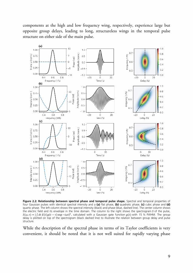
9
components at the high and low frequency wing, respectively, experience large but opposite group delays, leading to long, structureless wings in the temporal pulse structure on either side of the main pulse.
Figure 2.2: Relationship between spectral phase and temporal pulse shape. Spectral and temporal properties of four Gaussian pulses with identical spectral intensity and a (a) flat phase, (b) quadratic phase, (c) cubic phase and (d) quartic phase. The left column shows the spectral intensity (black) and phase (blue, dashed line). The center column shows the electric field and its envelope in the time domain. The column to the right shows the spectrogram 𝑆 of the pulse, 𝑆(𝜔, 𝜏) = | 𝑑𝑡 𝐸(𝑡)𝑔(𝑡 − 𝜏) exp −𝑖𝜔𝑡| , calculated with a Gaussian gate function 𝑔(𝑡) with 15 fs FWHM. The group delay is plotted on top of the spectrogram (black dashed line) to illustrate the relation between group delay and pulse structure.
While the description of the spectral phase in terms of its Taylor coefficients is very convenient, it should be noted that it is not well suited for rapidly varying phase
10
functions such as sinusoidal phases35 or phase jumps which occur in the context of pulse sequence generation36,37 or coherent control experiments38.
2.1.2 Dispersion and dispersion control
As shown above, the spectral phase can dramatically alter the shape and duration of an ultrashort laser pulse. In any laser application where short pulses are required it is therefore essential to control the spectral phase to ensure that the pulses have the shortest possible duration when interacting with the sample. The principal source of undesired spectral phase contributions in ultrafast optics setups is material dispersion from transmissive optical elements such as lenses, optical windows, or filters. These elements typically consist of optical glasses such as fused silica, which are practically transparent in the visible and near-infrared spectral region. Their optical properties can therefore be accurately described by a real-valued refractive index 𝑛. In dispersive materials, the refractive index varies with frequency and therefore both the phase velocity and the group velocity are frequency-dependent, causing broadband pulses to stretch in time as they propagate through the medium.
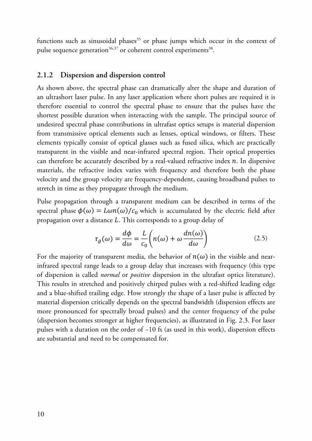
Pulse propagation through a transparent medium can be described in terms of the spectral phase 𝜙(𝜔) = 𝐿𝜔𝑛(𝜔)/𝑐 which is accumulated by the electric field after propagation over a distance 𝐿. This corresponds to a group delay of 𝜏 (𝜔) = 𝑑𝜙𝑑𝜔 = 𝐿𝑐 𝑛(𝜔) + 𝜔 𝑑𝑛(𝜔)𝑑𝜔 (2.5)
For the majority of transparent media, the behavior of 𝑛(𝜔) in the visible and near-infrared spectral range leads to a group delay that increases with frequency (this type of dispersion is called normal or positive dispersion in the ultrafast optics literature). This results in stretched and positively chirped pulses with a red-shifted leading edge and a blue-shifted trailing edge. How strongly the shape of a laser pulse is affected by material dispersion critically depends on the spectral bandwidth (dispersion effects are more pronounced for spectrally broad pulses) and the center frequency of the pulse (dispersion becomes stronger at higher frequencies), as illustrated in Fig. 2.3. For laser pulses with a duration on the order of ~10 fs (as used in this work), dispersion effects are substantial and need to be compensated for.

11
Figure 2.3: Pulse stretching due to material dispersion. The graph shows the initial and final pulse duration of a transform limited pulse propagating through 5 mm of fused silica (FS) glass which is commonly used for optical elements. Here, only second-order phase contributions are taken into account. The final pulse duration is shown for pulses centered at 700 nm (red) and 265 nm (blue).
Expanding the group delay 𝜏 (𝜔) in powers of the optical frequency 𝜔 reveals that pulse shape distortions due to dispersion are dominated by a linear group delay variation (corresponding to the quadratic phase term in equation (2.4)). To compensate for this, an optical setup with negative dispersion is required, i.e., a setup that introduces larger group delays for the low-frequency components of a laser pulse. Fortunately, various such setups are available: In prism compressors33,39 and grating compressors33, angular dispersion is used to create a frequency dependent optical path length with negative dispersion. So-called chirped mirrors40 have a specially designed coating that reflects different spectral components at a frequency-dependent penetration depth, also resulting in negative dispersion. Using either of these setups, it is possible to compensate for the linear group delay variation from material dispersion and achieve efficient pulse compression. However, higher-order variations of 𝜏 (𝜔) – which are relevant for the compression of pulses in the sub-10 fs regime – are more challenging to compensate since none of the above-mentioned components is capable of compensating first and higher-order group delay variations simultaneously. Prism compressors, for instance, overcompensate the quadratic group delay variation (third-order phase), leading to satellite pulses when compressing large bandwidth pulses. A more flexible (but also more complex) approach to dispersion compensation is adaptive pulse shaping, which can correct for dispersion contributions of all orders simultaneously37,41. Pulse shaping is discussed in more detail below.
2.1.2.1 Dispersive ray tracing Optical setups that rely on angular dispersion of spectral components to achieve temporal dispersion compensation – such as prism sequences or grating compressors –
12
are nowadays routinely used in laser setups, and analytic expressions are available to evaluate their temporal dispersion. These expressions are typically based on some approximations and simplifying assumptions (for instance, only paraxial rays are considered, or prisms are assumed to be oriented for minimum deviation) and they quickly become lengthy if more than a few optical elements are involved. For complex setups where these assumptions do not hold, it is therefore more convenient to calculate the temporal dispersion numerically using dispersive ray tracing. As the name suggests, the technique is based on ray optics, i.e., different spectral components are treated as optical rays whose path through the optical setup is traced numerically taking dispersion, reflection, refraction at interfaces and grating diffraction into account. By repeatedly tracing rays of different optical frequencies, it is possible to obtain the frequency-dependent optical path length 𝑃(𝜔) which contains the full information about the temporal dispersion of the setup33. In addition, ray tracing provides useful information about the angular and spatial dispersion introduced by optical setups. In Paper I, we investigated the temporal dispersion of a setup for broadband UV-pulse generation. Due to the complexity of the setup, an analytic evaluation of the dispersion was unfeasible and numerical ray tracing was employed instead. In addition, ray tracing was used to determine the setup configuration resulting in optimum phase-matching conditions for UV generation. In Paper II, dispersive ray tracing was employed to investigate how temporal and spatial dispersion of a grating-based interferometer are affected if deviations from the ideal (dispersion-free) alignment are introduced.
2.2 Fourier Transform Pulse Shaping
In the previous section on dispersion and pulse compression, we have already encountered several ways to manipulate the temporal shape of femtosecond laser pulses by controlling their spectral phase. For example, by combining a pulse compressor with a variable amount of glass in the beam path, one may create pulses with a tunable chirp30,42. Even the action of a Michelson interferometer, which creates two replica pulses at a controllable time separation, may be considered as a form of femtosecond pulse shaping. While these ‘conventional’ approaches to pulse shaping are of essential importance and ubiquitous within ultrafast optics, they typically provide only a few free control parameters, and the space of available temporal pulse shapes is limited. Efforts to overcome this limitation have been ongoing since the 1980s43. Nowadays, a range of advanced femtosecond pulse shaping techniques for the generation of nearly arbitrarily shaped optical pulses are available37,44, and these

13
methods are widely used in applications such as coherent control45,46, pulse compression, and multidimensional spectroscopy36,47. In combination with TR-PEEM, pulse shaping has been used to control spatial and temporal behavior of plasmonic excitations48,49 and in implementations of spatially-resolved two-dimensional spectroscopy50. Part of the work behind this thesis was the construction and calibration of a liquid crystal-based pulse shaper which will be incorporated into the TR-PEEM setup for future experiments. Special care was taken to compensate for interference artifacts which impair the accuracy of such devices, and the results from these efforts are reported in Paper III. In the remaining part of this section, I will introduce some general aspects of Fourier transform pulse shaping and provide a brief description of liquid crystal based pulse shapers.
Figure 2.4: The 4f-line. The spectral components of the ingoing pulse are angularly dispersed using a grating before being recollimated and focused by a lens or curved mirror. For pulse shaping, a spatial mask is placed in the Fourier plane at the center of the setup to manipulate the spatially separated spectral components.
Many pulse shaping implementations are based on the concept of Fourier transform pulse shaping, where the desired temporal pulse shape is synthesized by manipulating the pulse in the frequency domain. In practice, this is accomplished by spatially separating the frequency components of the input pulse and applying a spatial mask that modifies the spectral components according to the desired pulse shape. The optical setup commonly used for this purpose – known as 4f-line – is shown in Fig. 2.4. This setup separates different spectral components spatially by first introducing an angular dispersion using a diffraction gratingB before collimating and focusing the spectral components with a lens or focusing mirror. A spatial mask is placed in the central Fourier plane of the setup, where the individual spectral components are spatially dispersed and focused. Depending on the type of mask, spectral phase and/or
B In principle, a prism can also be used, see ref. 250. Prism-based pulse shapers offer high throughput and
put no constraints on the spectral pulse width, but the material dispersion introduced by the prism itself is substantial.
14
amplitude and/or polarization of the spectral components can be adjusted before they are recombined again to form the pulse with the desired temporal shape.
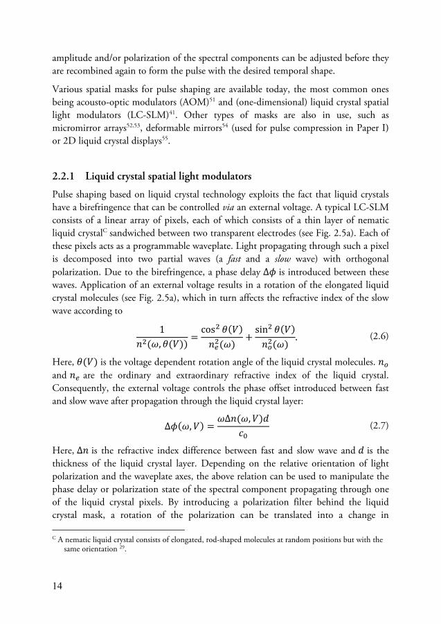
Various spatial masks for pulse shaping are available today, the most common ones being acousto-optic modulators (AOM)51 and (one-dimensional) liquid crystal spatial light modulators (LC-SLM)41. Other types of masks are also in use, such as micromirror arrays52,53, deformable mirrors54 (used for pulse compression in Paper I) or 2D liquid crystal displays55.
2.2.1 Liquid crystal spatial light modulators
Pulse shaping based on liquid crystal technology exploits the fact that liquid crystals have a birefringence that can be controlled via an external voltage. A typical LC-SLM consists of a linear array of pixels, each of which consists of a thin layer of nematic liquid crystalC sandwiched between two transparent electrodes (see Fig. 2.5a). Each of these pixels acts as a programmable waveplate. Light propagating through such a pixel is decomposed into two partial waves (a fast and a slow wave) with orthogonal polarization. Due to the birefringence, a phase delay Δ𝜙 is introduced between these waves. Application of an external voltage results in a rotation of the elongated liquid crystal molecules (see Fig. 2.5a), which in turn affects the refractive index of the slow wave according to 1𝑛 (𝜔, 𝜃(𝑉)) = cos 𝜃(𝑉)𝑛 (𝜔) + sin 𝜃(𝑉)𝑛 (𝜔) . (2.6)
Here, 𝜃(𝑉) is the voltage dependent rotation angle of the liquid crystal molecules. 𝑛 and 𝑛 are the ordinary and extraordinary refractive index of the liquid crystal. Consequently, the external voltage controls the phase offset introduced between fast and slow wave after propagation through the liquid crystal layer: Δ𝜙(𝜔, 𝑉) = 𝜔Δ𝑛(𝜔, 𝑉)𝑑𝑐 (2.7)
Here, Δ𝑛 is the refractive index difference between fast and slow wave and 𝑑 is the thickness of the liquid crystal layer. Depending on the relative orientation of light polarization and the waveplate axes, the above relation can be used to manipulate the phase delay or polarization state of the spectral component propagating through one of the liquid crystal pixels. By introducing a polarization filter behind the liquid crystal mask, a rotation of the polarization can be translated into a change in
C A nematic liquid crystal consists of elongated, rod-shaped molecules at random positions but with the same orientation 29.
15
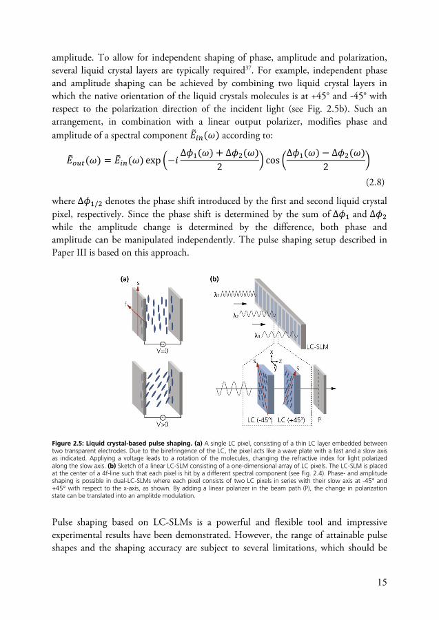
amplitude. To allow for independent shaping of phase, amplitude and polarization, several liquid crystal layers are typically required37. For example, independent phase and amplitude shaping can be achieved by combining two liquid crystal layers in which the native orientation of the liquid crystals molecules is at +45° and -45° with respect to the polarization direction of the incident light (see Fig. 2.5b). Such an arrangement, in combination with a linear output polarizer, modifies phase and amplitude of a spectral component 𝐸 (𝜔) according to: 𝐸 (𝜔) = 𝐸 (𝜔) exp −𝑖 Δ𝜙 (𝜔) + Δ𝜙 (𝜔)2 cos Δ𝜙 (𝜔) − Δ𝜙 (𝜔)2
(2.8)
where Δ𝜙 / denotes the phase shift introduced by the first and second liquid crystal pixel, respectively. Since the phase shift is determined by the sum of Δ𝜙 and Δ𝜙 while the amplitude change is determined by the difference, both phase and amplitude can be manipulated independently. The pulse shaping setup described in Paper III is based on this approach.
Figure 2.5: Liquid crystal-based pulse shaping. (a) A single LC pixel, consisting of a thin LC layer embedded between two transparent electrodes. Due to the birefringence of the LC, the pixel acts like a wave plate with a fast and a slow axis as indicated. Appliying a voltage leads to a rotation of the molecules, changing the refractive index for light polarized along the slow axis. (b) Sketch of a linear LC-SLM consisting of a one-dimensional array of LC pixels. The LC-SLM is placed at the center of a 4f-line such that each pixel is hit by a different spectral component (see Fig. 2.4). Phase- and amplitude shaping is possible in dual-LC-SLMs where each pixel consists of two LC pixels in series with their slow axis at -45° and +45° with respect to the x-axis, as shown. By adding a linear polarizer in the beam path (P), the change in polarization state can be translated into an amplitde modulation.
Pulse shaping based on LC-SLMs is a powerful and flexible tool and impressive experimental results have been demonstrated. However, the range of attainable pulse shapes and the shaping accuracy are subject to several limitations, which should be

16
considered in the planning and evaluation of pulse shaper-based experiments. Certain limitations arise from the general concept of Fourier transform pulse shaping in a 4f-line, such as spatio-temporal coupling56 (a change in the spatial pulse profile which is coupled to the frequency domain modulation introduced by the spatial mask) and the presence of a limited time window in which the real output pulse can accurately represent the programmed pulse shape57,58. Other limitations are related to specific classes of spatial masks. In the case of LC-SLMs, thermal motion of the liquid crystal introduces phase noise59 and the pixelation of the mask can lead to replica pulses in the time domain60. Another source of distortions in LC-SLMs is the multi-layer structure of these devices. Differences in refractive index between consecutive layers give rise to partial reflections which interfere with the main pulse, leading to unwanted spectral modulations of the output pulses. In Paper III, we characterize these interferences and describe how to correct for them by extending the standard calibration procedure for LC-SLMs.
2.3 Nonlinear optics
So far, we have limited the discussion of ultrafast pulses interacting with dielectric media to the linear regime, where the polarization induced by a laser pulse in the material is proportional to the optical field amplitude. In a non-dispersive medium, this polarization 𝑷(𝑡) is given by: 𝑃 (𝑡) = 𝜀 𝜒( )𝐸 (𝑡) (2.9)
The relation between electric field and polarization is determined by the linear susceptibility 𝜒( ) which is a 3 × 3 matrix in an anisotropic medium. One of the outstanding characteristics of ultrashort laser pulses is the extremely high peak intensity that can be reached since the output energy of femtosecond lasers is concentrated within an exceptionally short time interval. With focused laser pulses it is therefore rather straightforward to reach the regime where the response of the medium can no longer considered to be linear and where nonlinear interaction between the laser field and the material becomes relevant. To describe this nonlinear regime, equation (2.9) is extended by adding terms of higher order in the electric field: 𝑃 = 𝜀 𝜒( )𝐸 + 𝜀 𝜒( )𝐸 𝐸 + 𝜀 𝜒( ) 𝐸 𝐸 𝐸 + ⋯ (2.10)
17
Second-order nonlinear effects are characterized by 𝜒( ), third-order effects by 𝜒( ) and so on. The higher-order terms appearing in the above equation describe a wide range of nonlinear optical phenomena, a detailed discussion of which can be found in the literature61,62. To illustrate some of the nonlinear processes relevant in this work, we consider the example of an external field 𝐸(𝑡) interacting with a dispersionless medium with a 𝜒( )-nonlinearity. For the sake of simplicity, we will consider only a single cartesian component of 𝑷 and 𝑬, related by one component of the 𝜒( ) tensor, so that we can express the second-order polarization as 𝑃( )(𝑡) = 𝜀 𝜒( )𝐸 (𝑡). For an electric field with two frequency components,
𝐸(𝑡) = 𝐸 exp(𝑖𝜔 𝑡) + 𝐸 exp(𝑖𝜔 𝑡) + 𝑐. 𝑐. (2.11)
the second-order polarization becomes:
𝑃( )(𝑡) = 𝜀 𝜒( )(𝐸 𝑒 + 𝐸 𝑒 + 𝑐. 𝑐. ) +𝜀 𝜒( )2(𝐸 𝐸 𝑒 ( ) + 𝑐. 𝑐. ) +𝜀 𝜒( )2(𝐸 𝐸∗𝑒 ( ) + 𝑐. 𝑐. ) +𝜀 𝜒( )2(|𝐸 | + |𝐸 | )
(2.12)
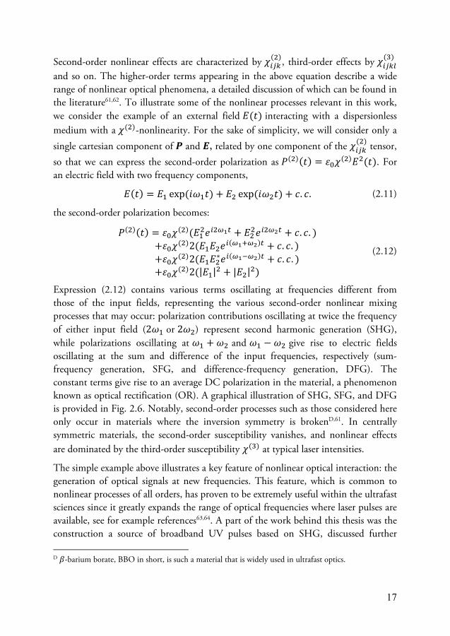
Expression (2.12) contains various terms oscillating at frequencies different from those of the input fields, representing the various second-order nonlinear mixing processes that may occur: polarization contributions oscillating at twice the frequency of either input field (2𝜔 or 2𝜔 ) represent second harmonic generation (SHG), while polarizations oscillating at 𝜔 + 𝜔 and 𝜔 − 𝜔 give rise to electric fields oscillating at the sum and difference of the input frequencies, respectively (sum-frequency generation, SFG, and difference-frequency generation, DFG). The constant terms give rise to an average DC polarization in the material, a phenomenon known as optical rectification (OR). A graphical illustration of SHG, SFG, and DFG is provided in Fig. 2.6. Notably, second-order processes such as those considered here only occur in materials where the inversion symmetry is brokenD,61. In centrally symmetric materials, the second-order susceptibility vanishes, and nonlinear effects are dominated by the third-order susceptibility 𝜒( ) at typical laser intensities.
The simple example above illustrates a key feature of nonlinear optical interaction: the generation of optical signals at new frequencies. This feature, which is common to nonlinear processes of all orders, has proven to be extremely useful within the ultrafast sciences since it greatly expands the range of optical frequencies where laser pulses are available, see for example references63,64. A part of the work behind this thesis was the construction a source of broadband UV pulses based on SHG, discussed further
D 𝛽-barium borate, BBO in short, is such a material that is widely used in ultrafast optics.
18
below and in Paper I. Nonlinear optical interactions are also the basis for the vast majority of methods for characterizing the temporal structure of ultrashort laser pulses, which have been essential in the pursuit of shorter and shorter laser pulse durations.
Figure 2.6: Second-order nonlinear frequency mixing processes. (a) Sum-frequency generation (SFG), (b) second harmonic generation (SHG), and (c) difference-frequency generation (DFG).
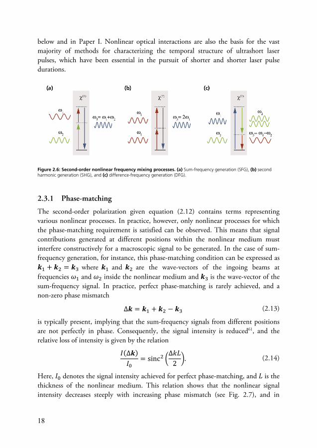
2.3.1 Phase-matching
The second-order polarization given equation (2.12) contains terms representing various nonlinear processes. In practice, however, only nonlinear processes for which the phase-matching requirement is satisfied can be observed. This means that signal contributions generated at different positions within the nonlinear medium must interfere constructively for a macroscopic signal to be generated. In the case of sum-frequency generation, for instance, this phase-matching condition can be expressed as 𝒌 + 𝒌 = 𝒌 where 𝒌 and 𝒌 are the wave-vectors of the ingoing beams at frequencies 𝜔 and 𝜔 inside the nonlinear medium and 𝒌 is the wave-vector of the sum-frequency signal. In practice, perfect phase-matching is rarely achieved, and a non-zero phase mismatch Δ𝒌 = 𝒌 + 𝒌 − 𝒌 (2.13)
is typically present, implying that the sum-frequency signals from different positions are not perfectly in phase. Consequently, the signal intensity is reduced61, and the relative loss of intensity is given by the relation 𝐼(Δ𝒌)𝐼 = sinc Δ𝑘𝐿2 . (2.14)
Here, 𝐼 denotes the signal intensity achieved for perfect phase-matching, and 𝐿 is the thickness of the nonlinear medium. This relation shows that the nonlinear signal intensity decreases steeply with increasing phase mismatch (see Fig. 2.7), and in
19
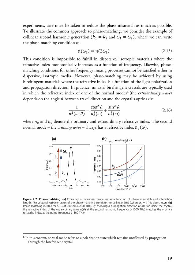
experiments, care must be taken to reduce the phase mismatch as much as possible. To illustrate the common approach to phase-matching, we consider the example of collinear second harmonic generation (𝒌 = 𝒌 and 𝜔 = 𝜔 ), where we can write the phase-matching condition as
𝑛(𝜔 ) = 𝑛(2𝜔 ). (2.15)
This condition is impossible to fulfill in dispersive, isotropic materials where the refractive index monotonically increases as a function of frequency. Likewise, phase-matching conditions for other frequency mixing processes cannot be satisfied either in dispersive, isotropic media. However, phase-matching may be achieved by using birefringent materials where the refractive index is a function of the light polarization and propagation direction. In practice, uniaxial birefringent crystals are typically used in which the refractive index of one of the normal modesE (the extraordinary wave) depends on the angle 𝜗 between travel direction and the crystal’s optic axis:
1𝑛 (𝜔, 𝜗) = cos 𝜗𝑛 (𝜔) + sin 𝜗𝑛 (𝜔) (2.16)
where 𝑛 and 𝑛 denote the ordinary and extraordinary refractive index. The second normal mode – the ordinary wave – always has a refractive index 𝑛 (𝜔).
Figure 2.7: Phase-matching. (a) Efficiency of nonlinear processes as a function of phase mismatch and interaction length. The vectorial representation of the phase-matching condition for collinear SHG (where 𝑘 = 𝑘 ) is also shown. (b) Phase-matching in BBO for SHG at 600 nm (~500 THz). By choosing a propagation direction at 40.24° inside the crystal, the refractive index of the extraordinary wave 𝑛(𝜗) at the second harmonic frequency (~1000 THz) matches the ordinary refractive index at the pump frequency (~500 THz).
E In this context, normal mode refers to a polarization state which remains unaffected by propagation
through the birefringent crystal.
20
The angular dependence of the refractive index introduces an additional degree of freedom that can be used to minimize the phase mismatch by choosing a suitable light polarization and crystal orientation. For example, in the widely used birefringent nonlinear crystal BBO, one finds that 𝑛 (𝜔) < 𝑛 (𝜔) at relevant optical frequencies, such that the phase-matching relation for SHG can be fulfilled with the pump beam (𝜔 ) as ordinary wave and the SHG signal (2𝜔 ) as extraordinary wave, as illustrated in Fig. 2.7b.
In the context of ultrafast optics, where nonlinear processes are often employed for amplification or frequency conversion of broadband pulses, an important parameter is the phase-matching bandwidth, i.e., the spectral bandwidth over which the phase mismatch is sufficiently small to allow for efficient nonlinear signal generation. In non-collinear geometries, a large phase-matching bandwidth can be achieved by carefully setting the angles of the ingoing beams and the crystal orientation65. A general approach, which also applies to collinear geometries, is the use of very thin nonlinear crystals, as the relative efficiency is determined by the product of phase mismatch and crystal length (see equation (2.14)). This approach has the disadvantage that a short interaction length limits the overall intensity of the nonlinear signal, and it is thus not feasible at low pulse energies. In Paper I, we use an alternative scheme known as achromatic phase-matching, where phase-matching for SHG over a large bandwidth is achieved by introducing a suitable angular dispersion in the incident pump beam. The small phase mismatch allows the use of relatively thick nonlinear crystals, making the approach attractive for generating broad UV pulses via SHG at low pulse energies.
2.3.2 Optical parametric amplification
Another second-order nonlinear process that is especially relevant for this work is DFG since this process can be used for the amplification of low-energy laser pulses in a scheme called optical parametric amplification (OPA). The amplification process is most conveniently illustrated in the photon picture, where we can understand DFG of light with energies ℏ𝜔 and ℏ𝜔 (with ℏ𝜔 > ℏ𝜔 ) as the destruction of a photon with ℏ𝜔 and the creation of a photon with the energy difference, ℏ(ω −ω ), see Fig. 2.6c. To satisfy energy and momentum conservation, an additional photon at energy ℏ𝜔 is generated in the process. The light at frequency 𝜔 – the pump beam – is thus depleted in the DFG process while the beam at 𝜔 – the seed – is amplified. In the amplification process, no energy is transferred to the nonlinear medium since the energy difference between pump and seed beam is released in the form photons (the process is said to be parametric). This immensely facilitates the
21
generation of intense laser pulses, since technical difficulties related to heating of the amplification medium are largely avoided. In a typical parametric amplification scheme, intense, narrow-band laser pulses are used as pump, while seed pulses are created through nonlinear white-light continuum generation via third-order nonlinear processes. Alternatively, the seed pulses may be generated directly by broadband oscillator systems65. By choosing suitable phase-matching conditions, a specific portion of the seed spectrum is amplified, enabling the generation of amplified, tunable, and spectrally broad laser pulses. OPA systems based on amplified solid-state lasers such as Ti:sapphire or Yb:KGWF lasers can generate femtosecond laser pulses throughout the visible (VIS) and near-infrared (NIR) spectral range66 and are nowadays widely used in ultrafast spectroscopy laboratories. Both the laser system used in Papers I to V and the system employed in Papers VI and VII are built around non-collinear optical parametric amplifiers (NOPAs). In NOPAs, the seed beam and the pump beam propagate non-collinearly through the amplification crystal, and the relative angle serves as an additional degree of freedom for adjusting the phase-matching conditions. Very large phase-matching bandwidths can be achieved in this fashion, enabling the generation of amplified few-fs pulses in the VIS spectral range25.
F Yb:KGW refers to ytterbium-doped potassium gadolinium tungstate, a gain medium used in
femtosecond lasers with a lasing transition around 1030 nm.

23
3 Light-Matter Interaction at the Nanoscale
This chapter is going to introduce the second main direction of research in this thesis: the photoexcitation dynamics triggered by femtosecond laser pulses when interacting with metal- and semiconductor nanostructures or surfaces. The discussion will focus on the systems and processes that are relevant for Papers IV to VII. The systems investigated in these papers can be divided into two categories: in Papers IV and V, we studied dynamics of photoexcited charge carriers in III-V semiconductor materials, in the form of bulk semiconductors (Paper V) and in the form of nanowires (Papers IV and V), needle-shaped nanocrystals with interesting properties. Section 3.1 introduces the III-V materials and III-V semiconductor nanowires. The relaxation dynamics of photoexcited electrons in these materials will be discussed in section 3.2, with a focus on intraband relaxation and transport processes unfolding on the femto- and picosecond time scale. In Papers VI and VII, we used TR-PEEM to investigate surface plasmon polaritons, excitations inherent to metal-dielectric interfaces that arise from the coupling between surface charge density oscillations and the optical electromagnetic field. Especially surface plasmon polaritons confined to the surfaces of nanoparticles have received much attention in recent decades (localized surface plasmons) since they can be used to create strongly localized and enhanced optical near-fields. Surface plasmon polaritons on surfaces and nanoparticles are introduced in section 3.3.
3.1 III-V compound semiconductors
III-V materials are semiconducting alloys consisting of one (or several) of the group III elements (mostly Al, Ga, In) of the periodic table and one (or several) of the group V elements (mostly N, P, As, Sb). These materials have been the subject of intense research for many decades, in large part due to their favorable optoelectronic properties: III-V semiconductors have large electron mobilities (especially the narrow-gap semiconductors InAs and InSb), and many III-V materials have a direct bandgap
24
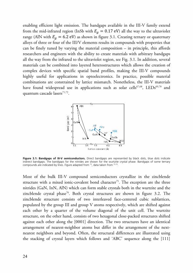
enabling efficient light emission. The bandgaps available in the III-V family extend from the mid-infrared region (InSb with 𝐸 = 0.17 eV) all the way to the ultraviolet range (AlN with 𝐸 = 6.2 eV) as shown in figure 3.1. Creating ternary or quaternary alloys of three or four of the III/V elements results in compounds with properties that can be finely tuned by varying the material composition – in principle, this affords researchers and engineers with the ability to create materials with arbitrary bandgaps all the way from the infrared to the ultraviolet region, see Fig. 3.1. In addition, several materials can be combined into layered heterostructures which allows the creation of complex devices with specific spatial band profiles, making the III-V compounds highly useful for applications in optoelectronics. In practice, possible material combinations are constrained by lattice mismatch. Nonetheless, the III-V materials have found widespread use in applications such as solar cells67,68, LEDs69,70 and quantum cascade lasers71,72.
Figure 3.1: Bandgaps of III-V semiconductors. Direct bandgaps are represented by black dots, blue dots indicate indirect bandgaps. The bandgaps for the nitrides are shown for the wurtzite crystal phase. Bandgaps of some ternary compounds are indicated by lines. Figure adapted from 73, data taken from 73,74.
Most of the bulk III-V compound semiconductors crystallize in the zincblende structure with a mixed ionic-covalent bond character75. The exception are the three nitrides (GaN, InN, AlN) which can form stable crystals both in the wurtzite and the zincblende crystal phase76. Both crystal structures are shown in figure 3.2. The zincblende structure consists of two interleaved face-centered cubic sublattices, populated by the group III and group V atoms respectively, which are shifted against each other by a quarter of the volume diagonal of the unit cell. The wurtzite structure, on the other hand, consists of two hexagonal close-packed structures shifted against each other along the [0001] direction. The two structures have an identical arrangement of nearest-neighbor atoms but differ in the arrangement of the next-nearest neighbors and beyond. Often, the structural differences are illustrated using the stacking of crystal layers which follows and ‘ABC’ sequence along the [111]
25
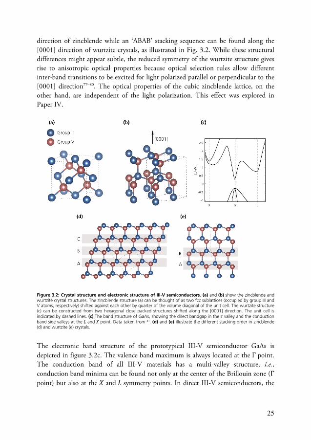
direction of zincblende while an ‘ABAB’ stacking sequence can be found along the [0001] direction of wurtzite crystals, as illustrated in Fig. 3.2. While these structural differences might appear subtle, the reduced symmetry of the wurtzite structure gives rise to anisotropic optical properties because optical selection rules allow different inter-band transitions to be excited for light polarized parallel or perpendicular to the [0001] direction77–80. The optical properties of the cubic zincblende lattice, on the other hand, are independent of the light polarization. This effect was explored in Paper IV.
Figure 3.2: Crystal structure and electronic structure of III-V semiconductors. (a) and (b) show the zincblende and wurtzite crystal structures. The zincblende structure (a) can be thought of as two fcc sublattices (occupied by group III and V atoms, respectively) shifted against each other by quarter of the volume diagonal of the unit cell. The wurtzite structure (c) can be constructed from two hexagonal close packed structures shifted along the [0001] direction. The unit cell is indicated by dashed lines. (c) The band structure of GaAs, showing the direct bandgap in the Γ valley and the conduction band side valleys at the 𝐿 and 𝑋 point. Data taken from 81. (d) and (e) illustrate the different stacking order in zincblende (d) and wurtzite (e) crystals.
The electronic band structure of the prototypical III-V semiconductor GaAs is depicted in figure 3.2c. The valence band maximum is always located at the Γ point. The conduction band of all III-V materials has a multi-valley structure, i.e., conduction band minima can be found not only at the center of the Brillouin zone (Γ point) but also at the 𝑋 and 𝐿 symmetry points. In direct III-V semiconductors, the

26
global conduction band minimum is located at the Γ point while it is located at the 𝑋 point in III-V semiconductor with an indirect bandgap such as GaP. The presence of conduction band side valleys has strong implications for the electronic properties of III-V materials because electrons that are either accelerated by strong electric fields or optically excited with high photon energies efficiently scatter into the side valleys via electron-phonon scattering82. This scattering mechanism reduces electron mobility in high fields. On the other hand, the inter-valley transfer may also be exploited in devices such as the Gunn oscillator82 and has been suggested as a mechanism to ‘store’ hot electrons for increased solar cell efficiency83,84.
3.1.1 III-V semiconductor nanowires
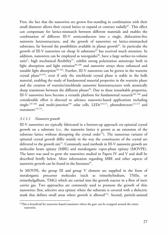
III-V semiconductor nanowires are needle-shaped single-crystalline nanostructures consisting of one or several of the III-V materials. III-V nanowires are characterized by a high aspect ratio, with the nanowire diameter typically in the range from 10 nm to 200 nm and nanowire lengths typically in the range of a few μm.
Growth of III-V nanowires was first observed in studies on planar semiconductor growth methods85,86 where nanowires could occur unintentionally under certain conditions87. First studies to systematically understand and optimize growth of III-V nanowires were undertaken in the early 1990s88,89 and efforts to fully understand the growth mechanisms involved are still ongoing90,91 although a high degree of control over the nanowire structure has been achieved by today92–94. This long-lasting interest in III-V nanowires is motivated by the unique properties of these quasi one-dimensional nanostructures in comparison with their bulk counterparts.
Figure 3.3: III-V semiconductor nanowires. (a) SEM image of a regular array of InAs nanowires grown via particle-assisted MOVPE. Image courtesy of Sebastian Lehman. (b) SEM image of InAs nanowires after transfer onto a silicon substrate for PEEM measurements. (c) SEM image of the top section of two GaAs nanowires, showing the characteristic gold seed particle at the nanowire top.
27
First, the fact that the nanowires are grown free-standing in combination with their small diameter allows their crystal lattice to expand or contract radially87. This effect can compensate for lattice-mismatch between different materials and enables the combination of different III-V semiconductors into a single, dislocation-free nanowire heterostructures, and the growth of nanowires on lattice-mismatched substrates, far beyond the possibilities available in planar growth87. In particular the growth of III-V nanowires on cheap Si substrates95 has received much attention. In addition, nanowires can be employed as waveguides96, have a large surface-to-volume ratioG, high mechanical flexibility97, exhibit strong polarization anisotropy both in light absorption and light emission98–100 and nanowire arrays show enhanced and tunable light absorption101,102. Further, III-V nanowires can be grown in the wurtzite crystal phase92,103, even if only the zincblende crystal phase is stable in the bulk material, enabling the study of fundamental material properties in the wurtzite phase and the creation of wurtzite/zincblende nanowire heterostructures with atomically sharp transitions between the different phases92. Due to these remarkable properties, III-V nanowires have become a versatile platform for fundamental research104–106 and considerable effort is directed to advance nanowire-based applications including single-107,108 and multi-junction109 solar cells, LEDs110,111, photodetectors112,113 and transistors114,115.
3.1.1.1 Nanowire growth III-V nanowires are typically fabricated in a bottom-up approach via epitaxial crystal growth on a substrate (i.e., the nanowire lattice is grown as an extension of the substrate lattice without disrupting the crystal order75). The numerous variants of epitaxial crystal growth differ mainly in the way the constituents of the crystal are delivered to the growth site75. Commonly used methods in III-V nanowire growth are molecular beam epitaxy (MBE) and metalorganic vapor-phase epitaxy (MOVPE). The latter was used to grow the nanowires studied in Papers IV and V and shall be described briefly below. More information regarding MBE and other aspects of nanowire growth can be found in the literature87.
In MOVPE, the group III and group V element are supplied in the form of metalorganic precursor molecules (such as trimethylindium, TMIn, or trimethylgallium, TMG) which are carried into the growth reactor in a flow of inert carrier gas. Two approaches are commonly used to promote the growth of thin nanowires: first, selective area epitaxy where the substrate is covered with a dielectric mask that defines small areas where growth is allowed116. Second, particle-assisted
GThis is beneficial for nanowire-based transistors where the gate can be wrapped around the entire
nanowire.
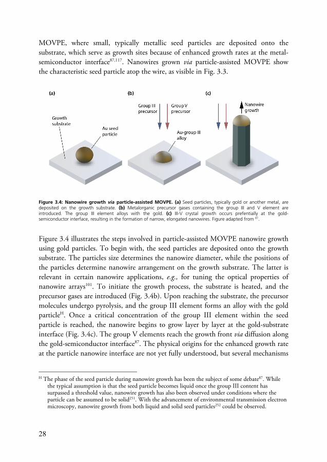
28
MOVPE, where small, typically metallic seed particles are deposited onto the substrate, which serve as growth sites because of enhanced growth rates at the metal-semiconductor interface87,117. Nanowires grown via particle-assisted MOVPE show the characteristic seed particle atop the wire, as visible in Fig. 3.3.
Figure 3.4: Nanowire growth via particle-assisted MOVPE. (a) Seed particles, typically gold or another metal, are deposited on the growth substrate. (b) Metalorganic precursor gases containing the group III and V element are introduced. The group III element alloys with the gold. (c) III-V crystal growth occurs prefentially at the gold-semiconductor interface, resulting in the formation of narrow, elongated nanowires. Figure adapted from 87.
Figure 3.4 illustrates the steps involved in particle-assisted MOVPE nanowire growth using gold particles. To begin with, the seed particles are deposited onto the growth substrate. The particles size determines the nanowire diameter, while the positions of the particles determine nanowire arrangement on the growth substrate. The latter is relevant in certain nanowire applications, e.g., for tuning the optical properties of nanowire arrays101. To initiate the growth process, the substrate is heated, and the precursor gases are introduced (Fig. 3.4b). Upon reaching the substrate, the precursor molecules undergo pyrolysis, and the group III element forms an alloy with the gold particleH. Once a critical concentration of the group III element within the seed particle is reached, the nanowire begins to grow layer by layer at the gold-substrate interface (Fig. 3.4c). The group V elements reach the growth front via diffusion along the gold-semiconductor interface87. The physical origins for the enhanced growth rate at the particle nanowire interface are not yet fully understood, but several mechanisms
H The phase of the seed particle during nanowire growth has been the subject of some debate87. While the typical assumption is that the seed particle becomes liquid once the group III content has surpassed a threshold value, nanowire growth has also been observed under conditions where the particle can be assumed to be solid251. With the advancement of environmental transmission electron microscopy, nanowire growth from both liquid and solid seed particles252 could be observed.
29
which are thought to be relevant have been identified: nucleation at the gold/nanowire interface is thermodynamically favored118, the gold particle may act as a catalyst lowering the activation energy for precursor pyrolysis119,120 and the gold particle may have an increased sticking coefficient, leading to accumulation of the growth materials at the nanowire top121.
Doping and material composition of the nanowire can be controlled by introducing dopants and by varying the precursor composition, respectively. In this fashion, complex nanowire heterostructures may be created, with both axial and radial segments. In addition, abrupt switching between wurtzite and zincblende crystal growth in the axial direction is possible by controlling the precursor ratios92.
3.2 Photoexcited electrons in semiconductors
The electronic structure of semiconductor materials is characterized by a forbidden gap separating the occupied valence band and the (nearly) empty conduction band. In the optical spectrum of a semiconductor, this shows as a sharp absorption onset at the bandgap energy 𝐸 . Exciting a semiconductor with an ultrashort optical pulse with photon energies ℏ𝜔 ≥ 𝐸 thus creates a nonequilibrium distribution of photoexcited electrons in the conduction band. Following such an excitation event, the semiconductor returns to equilibrium through a multitude of relaxation and transport processes, many of which take place on a femto- or picosecond time scale. Studies of this relaxation cascade, such as Papers IV and V, provide insight into fundamental processes in semiconductors and are immensely useful for the improvement of (opto-) electronic devices. The following section will provide a short overview on electron relaxation (3.3.1) and transport (3.3.2) on ultrashort time scales.
3.2.1 Carrier relaxation
The relaxation of photoexcited electrons in semiconductors is a complex interplay of numerous scattering and recombination processes, leading to dissipation of excess energy, momentum randomization and eventually to the restoration of equilibrium via recombination of photoexcited electrons and holes. For a discussion of this relaxation cascade, it is convenient to break down the entire process into four regimes6: (i) the coherent regime where excitations in the material have a well-defined phase, (ii) the emergence of a thermal hot carrier distribution via fast scattering processes, (iii) cooling of the hot carrier distribution and (iv) recombination of excited carriers. This picture is justified by the difference in the typical time scales of
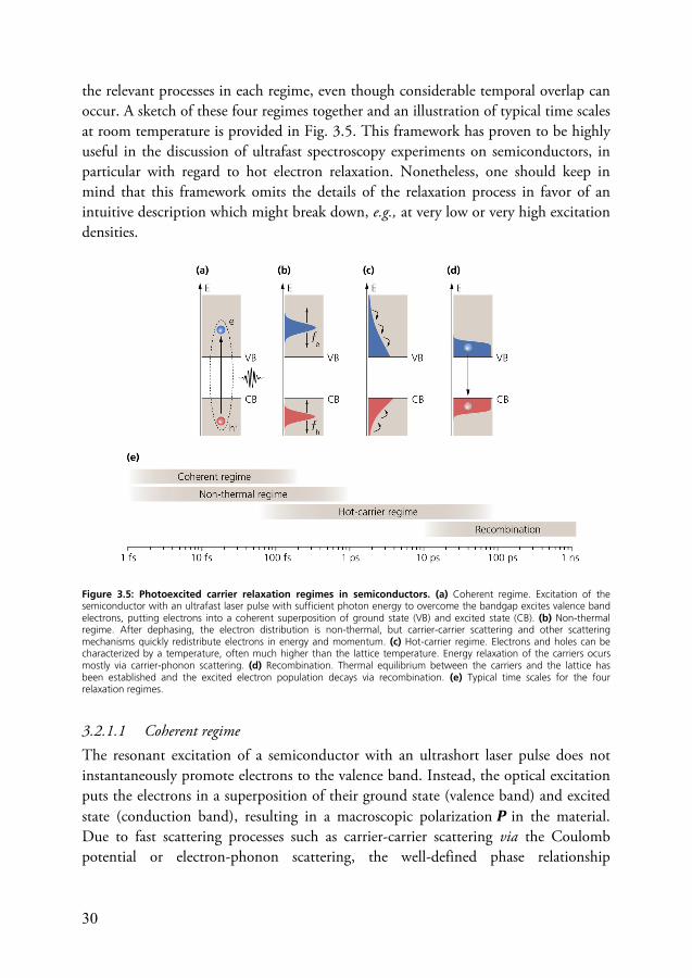
30
the relevant processes in each regime, even though considerable temporal overlap can occur. A sketch of these four regimes together and an illustration of typical time scales at room temperature is provided in Fig. 3.5. This framework has proven to be highly useful in the discussion of ultrafast spectroscopy experiments on semiconductors, in particular with regard to hot electron relaxation. Nonetheless, one should keep in mind that this framework omits the details of the relaxation process in favor of an intuitive description which might break down, e.g., at very low or very high excitation densities.
Figure 3.5: Photoexcited carrier relaxation regimes in semiconductors. (a) Coherent regime. Excitation of the semiconductor with an ultrafast laser pulse with sufficient photon energy to overcome the bandgap excites valence band electrons, putting electrons into a coherent superposition of ground state (VB) and excited state (CB). (b) Non-thermal regime. After dephasing, the electron distribution is non-thermal, but carrier-carrier scattering and other scattering mechanisms quickly redistribute electrons in energy and momentum. (c) Hot-carrier regime. Electrons and holes can be characterized by a temperature, often much higher than the lattice temperature. Energy relaxation of the carriers ocurs mostly via carrier-phonon scattering. (d) Recombination. Thermal equilibrium between the carriers and the lattice has been established and the excited electron population decays via recombination. (e) Typical time scales for the four relaxation regimes.
3.2.1.1 Coherent regime The resonant excitation of a semiconductor with an ultrashort laser pulse does not instantaneously promote electrons to the valence band. Instead, the optical excitation puts the electrons in a superposition of their ground state (valence band) and excited state (conduction band), resulting in a macroscopic polarization 𝑷 in the material. Due to fast scattering processes such as carrier-carrier scattering via the Coulomb potential or electron-phonon scattering, the well-defined phase relationship
31
(coherence) between the excitations in the material rapidly decays. The time scale of this decay is influenced by numerous factors such as excitation energy, excited electron density, temperature and electron-phonon coupling strength. In GaAs at room temperature, for example, polarization dephasing times around 10 fs have been reported122 for excitation densities on the order of ~1017 cm-3, while a dephasing time of 7 ps has been measured in the same material123 at liquid helium temperature and at excitation densities around ~1014 cm-3. In the experiments carried in this work (room temperature, excitation densities around ~1017 cm-3) dephasing times no longer than few tens of femtoseconds can be expected.
3.2.1.2 Non-thermal regime After dephasing, the excited carrier population in the material generally can be expected to be non-thermal, i.e., the energy distribution of the carriers does not follow a Fermi-Dirac distribution and it is therefore not possible to assign a temperature to the carriers. For sufficiently high excitation densities, this non-thermal distribution rapidly evolves into a thermal Fermi-Dirac distribution through carrier-carrier and carrier-phonon scattering in a process referred to as thermalizationI. The process often occurs on extremely short time scales (few tens of femtoseconds) and results in a redistribution of the excited electrons over a wide energy range124,125. On a similar time scale, carrier-carrier and carrier-phonon scattering processes also reshape the momentum distribution of the excited carriers and can lead to rapid and efficient electron transfer to conduction band side valleys126,127. In III-V semiconductors, for instance, electrons at high energies in the Γ-valley of the conduction band can be transferred into the 𝐿-valley via electron-phonon scattering within 100 fs or less126–130. The return from the side valleys to the Γ-valley is often substantially slower.
3.2.1.3 Hot carrier regime After thermalization, the electron distribution function follows the Fermi-Dirac statistics, i.e., it is possible to assign a temperature to the excited electrons (and holes). The initial electron temperature depends on excitation fluence and photon energy and can reach up to several thousands of Kelvins131, motivating the term ‘hot carriers’ which is often applied in this context. Mainly through interaction with phonons, the excess energy of the hot carriers is dissipated until thermal equilibrium between the hot carriers and the lattice is established. The time scale of this carrier cooling may
I Some authors use the term thermalization to describe the thermal equilibration of electrons and
phonons. In this thesis, and in Paper IV, thermalization refers to the evolution of the non-thermal electron distribution towards a thermal distribution.
32
vary between ~1 ps and hundreds of ps, depending on parameters such as electron-phonon coupling strength, lattice temperature, and density of excited electrons.
Electrons scatter with phonons via the deformation potential (the perturbation of the periodic lattice potential due to lattice deformations by phonons) and via the polarization induced by optical phonons in polar crystals, such as the III-V semiconductors. Longitudinal optical (LO) phonons, in particular, couple strongly to electrons in polar materials, and electron-LO-phonon scattering is typically assumed to be the dominant intra-band relaxation mechanism in such materials. Interestingly, the contributions of different phonon modes to the overall hot electron relaxation rate are still actively investigated132, with some studies challenging the established notion that hot carriers in polar materials lose their energy mainly through LO-phonon scattering133. At high excitation densities, the energy loss rate of hot carriers can decrease significantly due to the so-called hot-phonon effect (or phonon bottleneck effect), a phenomenon which has been explored intensely in the 1980s and 90s and which has recently received renewed attention in the context of lead-halide perovskite materials131. The effect occurs when the comparatively slow anharmonic decay of optical phonons into acoustic phonons leads to a large non-equilibrium optical phonon population, increasing the rate of phonon reabsorption by electrons and thus lowering the net cooling rate of the hot carriers6,131,132. The change in the effective cooling time due to hot phonon effects can be dramatic, extending the time scale for equilibration between electrons and lattice by a factor of up to ~100131,134.
While electron-phonon scattering is often the prevalent mechanism for hot electron cooling, other energy relaxation channels may also play an important role. In narrow-gap semiconductors like InAs or InSb, for example, hot electrons can relax via impact ionization126,130, an inelastic scattering process in which a conduction band electron transfers energy to a valence band electron, thereby promoting it to the conduction band135. Impact ionization thus both reduces the average kinetic energy of the conduction band electrons (cooling) and also leads to an increased number of free carriers in the conduction band.
Another mechanism which can lead to rapid cooling of the hot electron distribution is electron-hole scattering136–140. In semiconductors where the effective hole mass 𝑚∗ significantly exceeds the effective electron mass 𝑚∗ , the electrons obtain most of the excess energy after optical excitation. After thermalization of each subsystem, this results in a large electron temperature 𝑇 and a comparatively low hole temperature 𝑇 ( 𝑇 ≫ 𝑇 ). Inelastic collisions between electrons and holes then lead to energy transfer from the hot electron distribution to the cold hole distribution, effectively cooling the electrons. Thermal equilibrium between electrons and holes with 𝑇 = 𝑇
33
is typically observed within less than 1 ps. However, large carrier densities are required for the energy loss rate due to electron-hole scattering to be relevant (in comparison to electron-phonon scattering)137,138 since the electron-hole collision rate strongly depends on the carrier density. In Paper IV, we discuss hot electron relaxation in InAs nanowires and find evidence that electron-hole scattering plays a major role in the electron cooling dynamics at early times (≤ 1ps).
3.2.1.4 Recombination Eventually, a photoexcited semiconductor returns to its ground state through recombination of the photoexcited charge carriers. Recombination can occur through multiple pathways whose relative importance depends on the material properties and the density of excited carriers. Generally, these processes can be divided into radiative processes where the excess energy is released in form of a photon, and non-radiative processes in which recombination occurs via the emission of multiple phonons.
Radiative recombination is significant only in direct bandgap semiconductors due to the small photon momentum. The direct recombination of a conduction band electron with a valence band hole under the release of a photon is referred to as bimolecular recombination. At low excitation densities, non-radiative recombination is dominated by trap states within the bandgap which capture free electrons or holes, which then recombine with free charges, releasing the excess energy in the form of phonons. Trap states are especially common at semiconductor surface, and surface-trap-assisted recombination (or simply ‘surface recombination’) can be the dominant carrier recombination process if the surface is not passivated141. Traps can also show optical activity, i.e., the recombination of trapped carriers can be accompanied by the release of a photon, observable as below-bandgap luminescence from semiconductors142. At high densities of excited carriers, Auger recombination where the excess energy is transferred to another charge carrier can become relevant.
The evolution of the excited carrier density in semiconductors is typically described by a set of rate equations143,144. A simple description of the decay of the excited electron density 𝑛 is provided by the so-called ‘ABC model’145 which gives the expression
𝑑𝑛 𝑑𝑡⁄ = −𝐴𝑛 − 𝐵𝑛 − 𝐶𝑛 . (3.1)
Here, 𝐴 is the (monomolecular) trapping rate constant, 𝐵 describes bimolecular recombination and the third-order term with coefficient 𝐶 accounts for Auger recombination. The density dependence of the different terms arises from the different number of carriers involved in the processes. Accordingly, an experimental
34
determination of the relationship between decay rate and carrier density provides clues about the relevant recombination channels.
3.2.2 Electron transport
Transport of photoexcited charge carriers on ultrashort time scales occurs as a result of internal or external electric fields or due to spatial charge density variations146. Understanding such light-induced transport processes is of crucial importance in the development of improved solar cells and light detectors. This section provides a brief overview over ultrafast (electron) transport processes at semiconductor surfaces which can be observed by surface-sensitive techniques such as time-resolved PEEM.
3.2.2.1 Diffusion A spatially inhomogeneous density of photoexcited electrons results in a diffusion current directed against the charge density gradient. In experiments where excited electrons are generated by focused laser pulses, a spatially non-uniform charge density inherently arises due to finite spot size of the excitation beam. However, whether or not diffusion becomes relevant strongly depends on the exact size of the excitation spot. In GaAs, for example, the electron diffusion coefficient can reach up to ~200 cm2/s at room temperature147, corresponding to typical diffusion lengths of ~1 μm and ~4 μm after 100 ps and 1 ns, respectively. If the initial excitation is confined on a length scale on the order the typical diffusion lengthJ, diffusion effects will be significant, while they might go unnoticed in experiments with weakly focused excitation beams. Notably, hot electrons show distinctly larger diffusivity as compared to ‘cold’ electrons148,149 and diffusion effects are hence particularly pronounced during the hot carrier regime of charge carrier relaxation.
In addition to lateral density variations, vertical variations of the density naturally occur when a strongly absorbing bulk material is optically excited due to the limited penetration depth of the light. The excitation depth can be estimated as 𝑑 ≈ 1/𝛼(𝜆) where 𝛼(𝜆) is the wavelength-dependent absorption coefficient. For example, for GaAs at photon energies just above the bandgap, we find 𝛼 ∼ 10 cm such that carriers will be predominantly generated in layer with a depth of ~1 μm at the sample surface. Provided that carriers have a sufficiently long lifetime, diffusion into the bulk can then lead to a depletion of charge carriers in the surface region.
J The characteristic length scale d depends on the time-span 𝑇 covered by the experiment via 𝑑 = √𝐷𝑇 where 𝐷 is the diffusion coefficient.
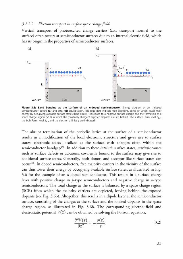
35
3.2.2.2 Electron transport in surface space charge fields Vertical transport of photoexcited charge carriers (i.e., transport normal to the surface) often occurs at semiconductor surfaces due to an internal electric field, which has its origin in the properties of semiconductor surfaces.
Figure 3.6: Band bending at the surface of an n-doped semiconductor. Energy diagram of an n-doped semiconductor before (a) and after (b) equilibration. The blue dots indicate free electrons, some of which lower their energy by occupying available surface states (blue arrow). This leads to a negative surface charge and the formation of a space charge region (SCR) in which the (positively charged) exposed dopants are left behind. The surface Fermi level 𝐸 , , the bulk Fermi level 𝐸 , and the electron affinity 𝜒 are indicated.
The abrupt termination of the periodic lattice at the surface of a semiconductor results in a modification of the local electronic structure and gives rise to surface states: electronic states localized at the surface with energies often within the semiconductor bandgap150. In addition to these intrinsic surface states, extrinsic causes such as surface defects or ad-atoms covalently bound to the surface may give rise to additional surface states. Generally, both donor- and acceptor-like surface states can occur150. In doped semiconductors, free majority carriers in the vicinity of the surface can thus lower their energy by occupying available surface states, as illustrated in Fig. 3.6 for the example of an n-doped semiconductor. This results in a surface charge layer with positive charge in p-type semiconductors and negative charge in n-type semiconductors. The total charge at the surface is balanced by a space charge region (SCR) from which the majority carriers are depleted, leaving behind the exposed dopants (see Fig. 3.6b). Altogether, this results in a dipole layer at the semiconductor surface, consisting of the charges at the surface and the ionized dopants in the space charge region, as illustrated in Fig. 3.6b. The corresponding electric field and electrostatic potential 𝑉(𝑧) can be obtained by solving the Poisson equation,
𝜕 𝑉(𝑧)𝜕𝑧 = − 𝜌(𝑧)𝜀 . (3.2)
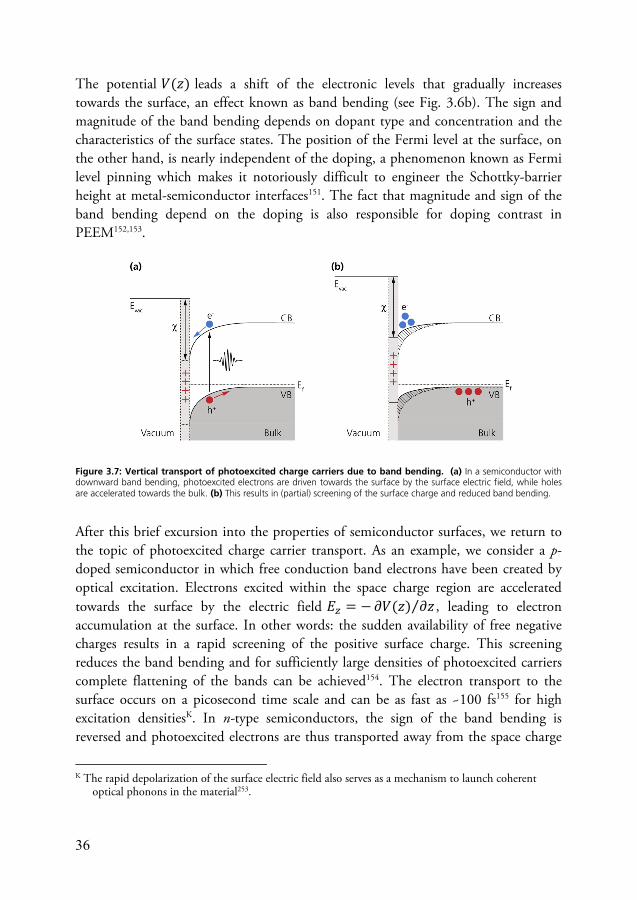
36
The potential 𝑉(𝑧) leads a shift of the electronic levels that gradually increases towards the surface, an effect known as band bending (see Fig. 3.6b). The sign and magnitude of the band bending depends on dopant type and concentration and the characteristics of the surface states. The position of the Fermi level at the surface, on the other hand, is nearly independent of the doping, a phenomenon known as Fermi level pinning which makes it notoriously difficult to engineer the Schottky-barrier height at metal-semiconductor interfaces151. The fact that magnitude and sign of the band bending depend on the doping is also responsible for doping contrast in PEEM152,153.
Figure 3.7: Vertical transport of photoexcited charge carriers due to band bending. (a) In a semiconductor with downward band bending, photoexcited electrons are driven towards the surface by the surface electric field, while holes are accelerated towards the bulk. (b) This results in (partial) screening of the surface charge and reduced band bending.
After this brief excursion into the properties of semiconductor surfaces, we return to the topic of photoexcited charge carrier transport. As an example, we consider a p-doped semiconductor in which free conduction band electrons have been created by optical excitation. Electrons excited within the space charge region are accelerated towards the surface by the electric field 𝐸 = − 𝜕𝑉(𝑧) 𝜕𝑧⁄ , leading to electron accumulation at the surface. In other words: the sudden availability of free negative charges results in a rapid screening of the positive surface charge. This screening reduces the band bending and for sufficiently large densities of photoexcited carriers complete flattening of the bands can be achieved154. The electron transport to the surface occurs on a picosecond time scale and can be as fast as ~100 fs155 for high excitation densitiesK. In n-type semiconductors, the sign of the band bending is reversed and photoexcited electrons are thus transported away from the space charge
K The rapid depolarization of the surface electric field also serves as a mechanism to launch coherent optical phonons in the material253.
37
region into the bulk. A notable exception is InAs which is well-known to have a large density of donor-like surface states above the conduction band minimum. For low to moderate n-doping concentrations, InAs thus exhibits downward band bending, resulting in the formation of a electron accumulation layer (as opposed to the more common electron depletion layer) at the surface. Ultrafast transport of photoexcited electrons in space charge fields at surfaces is observed in the TR-PEEM experiments reported in Papers IV and V.
3.3 Surface plasmon polaritons
Surface plasmon polaritons (SPPs) are electromagnetic waves confined to metal-dielectric interfaces, coupled to collective oscillations to the free electron plasma at the metal surface. While extended interfaces support propagating SPP modes, small metal nanoparticles give rise to non-propagating oscillations of the surface electrons coupled to an electromagnetic field. These resonances are called localized surface plasmons (LSPs). The research field that deals with the properties of these excitations is called plasmonics.
Both localized and propagating surface plasmons have been the subject of intense research, in large parts due to the fact that optical excitation of LSPs in metal nanostructures can result in strongly localized and enhanced optical near-fields156. This effect is, for instance, used to enhance nonlinear frequency mixing processes157, to dramatically increase otherwise weak signals in surface-enhanced Raman spectroscopy158, for molecular sensing159, or to localize optical excitations far beyond the optical diffraction limit160. In addition, the possibility for nanoscale confinement and guiding of electromagnetic waves at optical frequencies has spurred efforts to create nanoscale plasmonic circuitry with the aim to bridge the gap between small, but slow semiconductor components and fast, but bulky conventional photonics14. While resistive losses in metals pose an immense challenge to these ambitions14, efforts to integrate plasmonic circuits with established technologies still continue161.
In Papers VI and VII, we have used TR-PEEM to investigate both propagating and localized surface plasmons. The aim of this section is to introduce some basic aspects of surface plasmon polaritons in order to provide the background for these studies. In section 3.3.1, I will describe the optical properties of the noble metals which are the most commonly used materials in plasmonic research. Propagating and localized surface plasmons are introduced in the following sections. The discussion of surface plasmon polaritons loosely follows the more detailed treatment given by Maier156.
38
3.3.1 The dielectric function of noble metals
In this section, we will briefly review the interaction between an optical electromagnetic field and a material (in particular the noble metals gold, silver, and copper) within the framework of classical electrodynamics. The behavior of electromagnetic fields in a medium is fully determined by the macroscopic Maxwell equations, which are discussed in the standard literature on classical electrodynamics162. Here, only non-magnetic materials are considered, and the discussion will thus focus on the electric field. In a material, an oscillating external electric field leads to a relative displacement of the atomic nuclei and the surrounding electron clouds, and thus induces a polarization 𝑷 in the material. Both the induced polarization and the external field contribute to the auxiliary displacement field 𝑫, which is given by
𝑫(𝒓, 𝑡) = 𝜀 𝑬(𝒓, 𝑡) + 𝑷(𝒓, 𝑡). (3.3)
The vacuum permittivity is denoted 𝜀 . In a material without permanent dipoles, the polarization 𝑷 only depends on the electric field, and the material’s response to optical fields is characterized by relationship between 𝑬 and 𝑷. In case of a dispersive, isotropic, and spatially homogeneous material, and for sufficiently weak fields, this relation is given by
𝑷(𝑡) = 𝜀 𝑑𝑡 𝜒(𝑡 − 𝑡 )𝑬(𝑡 ). (3.4)
Here, 𝜒 denotes the (linear) susceptibility of the material which we have already encountered in chapter 2. It contains all information about the linear optical properties of the material and depends on the instantaneous field amplitude as well as the field strength at past time points if the material is dispersive. In the frequency domain, the relation between polarization and electric field becomes 𝑷(𝜔) =𝜀 𝜒(𝜔)𝑬(𝜔), and the displacement field is then given by
𝑫(𝜔) = 𝜀 𝜀(𝜔)𝑬(𝜔). (3.5)
Here, we have introduced the dielectric function 𝜀(𝜔) = 1 + 𝜒(𝜔). While we have thus far treated the electromagnetic field and the material response in the classical picture, the electronic structure of the material (and thus its quantum mechanical description) enter the picture via the dielectric function. The electronic structure of the three noble metals most relevant in plasmonics (Au, Ag and Cu) is characterized by a partly filled sp-band with a free electron-like parabolic dispersion, and completely filled, flat d-bands, as sketched in Fig. 3.8a. The optical properties of these metals are then determined by the quasi-free electrons occupying the sp-band around the Fermi level, and by inter-band transitions from the d-band to the sp-band.
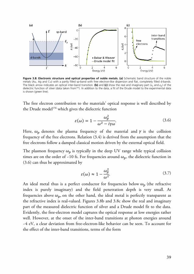
39
Figure 3.8: Electronic structure and optical properties of noble metals. (a) Schematic band structure of the noble metals (Au, Ag and Cu) with a partly filled sp-band with free electron-like dispersion and flat, completely filled d-bands. The black arrow indicates an optical inter-band transition. (b) and (c) show the real and imaginary part (𝜀 and 𝜀 ) of the dielectric function of silver (data taken from163). In addition to the data, a fit of the Drude model to the experimental data is shown (green line).
The free electron contribution to the materials’ optical response is well described by the Drude model156 which gives the dielectric function
𝜀(𝜔) = 1 − 𝜔𝜔 − 𝑖γ𝜔. (3.6)
Here, 𝜔 denotes the plasma frequency of the material and 𝛾 is the collision frequency of the free electrons. Relation (3.4) is derived from the assumption that the free electrons follow a damped classical motion driven by the external optical field.
The plasmon frequency 𝜔 is typically in the deep UV range while typical collision times are on the order of ~10 fs. For frequencies around 𝜔 , the dielectric function in (3.6) can thus be approximated by
𝜀(𝜔) ≈ 1 − 𝜔𝜔 . (3.7)
An ideal metal thus is a perfect conductor for frequencies below 𝜔 (the refractive index is purely imaginary) and the field penetration depth is very small. At frequencies above 𝜔 , on the other hand, the ideal metal is perfectly transparent as the refractive index is real-valued. Figures 3.8b and 3.8c show the real and imaginary part of the measured dielectric function of silver and a Drude model fit to the data. Evidently, the free-electron model captures the optical response at low energies rather well. However, at the onset of the inter-band transitions at photon energies around ~4 eV, a clear deviation from free-electron-like behavior can be seen. To account for the effect of the inter-band transitions, terms of the form
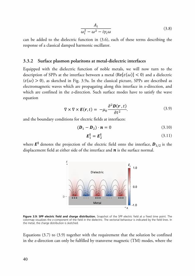
40
𝐴𝜔 − 𝜔 − 𝑖𝛾 𝜔 (3.8)
can be added to the dielectric function in (3.6), each of these terms describing the response of a classical damped harmonic oscillator.
3.3.2 Surface plasmon polaritons at metal-dielectric interfaces
Equipped with the dielectric function of noble metals, we will now turn to the description of SPPs at the interface between a metal (Re[𝜀(𝜔)] < 0) and a dielectric (𝜀(𝜔) > 0), as sketched in Fig. 3.9a. In the classical picture, SPPs are described as electromagnetic waves which are propagating along this interface in x-direction, and which are confined in the z-direction. Such surface modes have to satisfy the wave equation ∇ × ∇ × 𝑬(𝒓, 𝑡) = −𝜇 𝜕 𝑫(𝒓 , 𝑡)𝜕𝑡 . (3.9)
and the boundary conditions for electric fields at interfaces: (𝑫 − 𝑫 ) ⋅ 𝒏 = 0 (3.10) 𝑬∥ = 𝑬∥ (3.11)
where 𝑬∥ denotes the projection of the electric field onto the interface, 𝑫 / is the displacement field at either side of the interface and 𝒏 is the surface normal.
Figure 3.9: SPP electric field and charge distribution. Snapshot of the SPP electric field at a fixed time point. The colormap visualizes the z-component of the field in the dielectric. The vectorial behaviour is indicated by the field lines. In the metal, the charge distribution is sketched.
Equations (3.7) to (3.9) together with the requirement that the solution be confined in the z-direction can only be fulfilled by transverse magnetic (TM) modes, where the
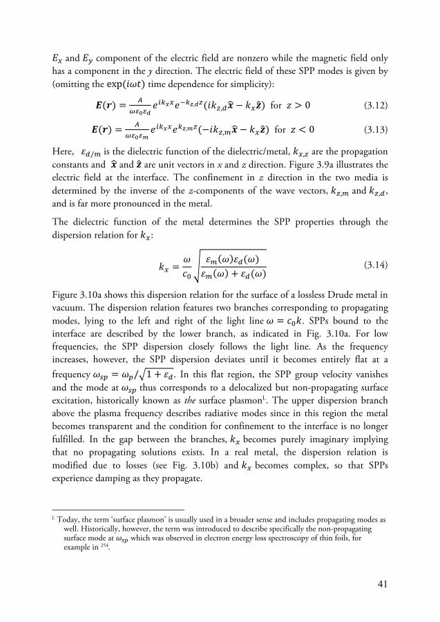
41
𝐸 and 𝐸 component of the electric field are nonzero while the magnetic field only has a component in the y direction. The electric field of these SPP modes is given by (omitting the exp(𝑖𝜔𝑡) time dependence for simplicity): 𝑬(𝒓) = 𝑒 𝑒 , (𝑖𝑘 , 𝒙 − 𝑘 𝒛) for 𝑧 > 0 (3.12) 𝑬(𝒓) = 𝑒 𝑒 , (−𝑖𝑘 , 𝒙 − 𝑘 𝒛) for 𝑧 < 0 (3.13)
Here, 𝜀 / is the dielectric function of the dielectric/metal, 𝑘 , are the propagation constants and 𝒙 and 𝒛 are unit vectors in x and z direction. Figure 3.9a illustrates the electric field at the interface. The confinement in z direction in the two media is determined by the inverse of the z-components of the wave vectors, 𝑘 , and 𝑘 , , and is far more pronounced in the metal.
The dielectric function of the metal determines the SPP properties through the dispersion relation for 𝑘 :
𝑘 = 𝜔𝑐 𝜀 (𝜔)𝜀 (𝜔) 𝜀 (𝜔) + 𝜀 (𝜔) (3.14)
Figure 3.10a shows this dispersion relation for the surface of a lossless Drude metal in vacuum. The dispersion relation features two branches corresponding to propagating modes, lying to the left and right of the light line 𝜔 = 𝑐 𝑘. SPPs bound to the interface are described by the lower branch, as indicated in Fig. 3.10a. For low frequencies, the SPP dispersion closely follows the light line. As the frequency increases, however, the SPP dispersion deviates until it becomes entirely flat at a frequency 𝜔 = 𝜔 / 1 + 𝜀 . In this flat region, the SPP group velocity vanishes and the mode at 𝜔 thus corresponds to a delocalized but non-propagating surface excitation, historically known as the surface plasmonL. The upper dispersion branch above the plasma frequency describes radiative modes since in this region the metal becomes transparent and the condition for confinement to the interface is no longer fulfilled. In the gap between the branches, 𝑘 becomes purely imaginary implying that no propagating solutions exists. In a real metal, the dispersion relation is modified due to losses (see Fig. 3.10b) and 𝑘 becomes complex, so that SPPs experience damping as they propagate.
L Today, the term ‘surface plasmon’ is usually used in a broader sense and includes propagating modes as
well. Historically, however, the term was introduced to describe specifically the non-propagating surface mode at 𝜔 which was observed in electron energy loss spectroscopy of thin foils, for example in 254.
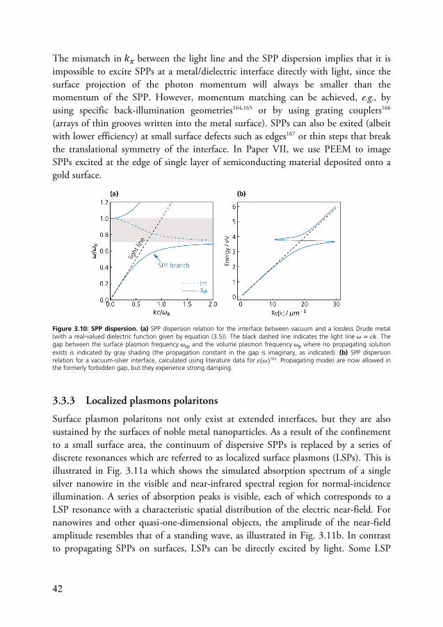
42
The mismatch in 𝑘 between the light line and the SPP dispersion implies that it is impossible to excite SPPs at a metal/dielectric interface directly with light, since the surface projection of the photon momentum will always be smaller than the momentum of the SPP. However, momentum matching can be achieved, e.g., by using specific back-illumination geometries164,165 or by using grating couplers166 (arrays of thin grooves written into the metal surface). SPPs can also be exited (albeit with lower efficiency) at small surface defects such as edges167 or thin steps that break the translational symmetry of the interface. In Paper VII, we use PEEM to image SPPs excited at the edge of single layer of semiconducting material deposited onto a gold surface.
Figure 3.10: SPP dispersion. (a) SPP dispersion relation for the interface between vacuum and a lossless Drude metal (with a real-valued dielectric function given by equation (3.5)). The black dashed line indicates the light line 𝜔 = 𝑐𝑘. The gap between the surface plasmon frequency 𝜔 and the volume plasmon frequency 𝜔 where no propagating solution exists is indicated by gray shading (the propagation constant in the gap is imaginary, as indicated). (b) SPP dispersion relation for a vacuum-silver interface, calculated using literature data for 𝜀(𝜔)163. Propagating modes are now allowed in the formerly forbidden gap, but they experience strong damping.
3.3.3 Localized plasmons polaritons
Surface plasmon polaritons not only exist at extended interfaces, but they are also sustained by the surfaces of noble metal nanoparticles. As a result of the confinement to a small surface area, the continuum of dispersive SPPs is replaced by a series of discrete resonances which are referred to as localized surface plasmons (LSPs). This is illustrated in Fig. 3.11a which shows the simulated absorption spectrum of a single silver nanowire in the visible and near-infrared spectral region for normal-incidence illumination. A series of absorption peaks is visible, each of which corresponds to a LSP resonance with a characteristic spatial distribution of the electric near-field. For nanowires and other quasi-one-dimensional objects, the amplitude of the near-field amplitude resembles that of a standing wave, as illustrated in Fig. 3.11b. In contrast to propagating SPPs on surfaces, LSPs can be directly excited by light. Some LSP
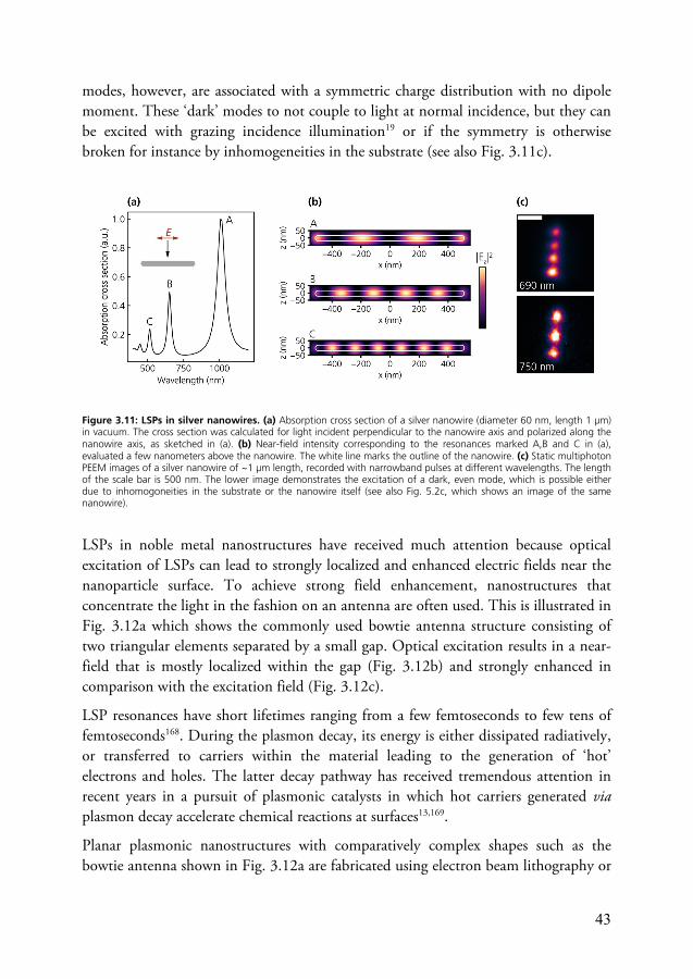
43
modes, however, are associated with a symmetric charge distribution with no dipole moment. These ‘dark’ modes to not couple to light at normal incidence, but they can be excited with grazing incidence illumination19 or if the symmetry is otherwise broken for instance by inhomogeneities in the substrate (see also Fig. 3.11c).
Figure 3.11: LSPs in silver nanowires. (a) Absorption cross section of a silver nanowire (diameter 60 nm, length 1 μm) in vacuum. The cross section was calculated for light incident perpendicular to the nanowire axis and polarized along the nanowire axis, as sketched in (a). (b) Near-field intensity corresponding to the resonances marked A,B and C in (a), evaluated a few nanometers above the nanowire. The white line marks the outline of the nanowire. (c) Static multiphoton PEEM images of a silver nanowire of ~1 μm length, recorded with narrowband pulses at different wavelengths. The length of the scale bar is 500 nm. The lower image demonstrates the excitation of a dark, even mode, which is possible either due to inhomogoneities in the substrate or the nanowire itself (see also Fig. 5.2c, which shows an image of the same nanowire).
LSPs in noble metal nanostructures have received much attention because optical excitation of LSPs can lead to strongly localized and enhanced electric fields near the nanoparticle surface. To achieve strong field enhancement, nanostructures that concentrate the light in the fashion on an antenna are often used. This is illustrated in Fig. 3.12a which shows the commonly used bowtie antenna structure consisting of two triangular elements separated by a small gap. Optical excitation results in a near-field that is mostly localized within the gap (Fig. 3.12b) and strongly enhanced in comparison with the excitation field (Fig. 3.12c).
LSP resonances have short lifetimes ranging from a few femtoseconds to few tens of femtoseconds168. During the plasmon decay, its energy is either dissipated radiatively, or transferred to carriers within the material leading to the generation of ‘hot’ electrons and holes. The latter decay pathway has received tremendous attention in recent years in a pursuit of plasmonic catalysts in which hot carriers generated via plasmon decay accelerate chemical reactions at surfaces13,169.
Planar plasmonic nanostructures with comparatively complex shapes such as the bowtie antenna shown in Fig. 3.12a are fabricated using electron beam lithography or
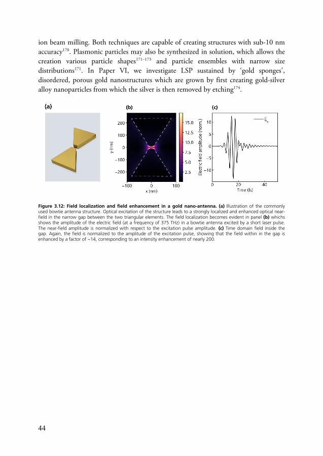
44
ion beam milling. Both techniques are capable of creating structures with sub-10 nm accuracy170. Plasmonic particles may also be synthesized in solution, which allows the creation various particle shapes171–173 and particle ensembles with narrow size distributions171. In Paper VI, we investigate LSP sustained by ‘gold sponges’, disordered, porous gold nanostructures which are grown by first creating gold-silver alloy nanoparticles from which the silver is then removed by etching174.
Figure 3.12: Field localization and field enhancement in a gold nano-antenna. (a) Illustration of the commonly used bowtie antenna structure. Optical excitation of the structure leads to a strongly localized and enhanced optical near-field in the narrow gap between the two triangular elements. The field localization becomes evident in panel (b) whichs shows the amplitude of the electric field (at a frequency of 375 THz) in a bowtie antenna excited by a short laser pulse. The near-field amplitude is normalized with respect to the excitation pulse amplitude. (c) Time domain field inside the gap. Again, the field is normalized to the amplitude of the excitation pulse, showing that the field within in the gap is enhanced by a factor of ~14, corresponding to an intensity enhancement of nearly 200.
45
4 Photoemission
Illuminating the surface of a solid with light of sufficiently high photon energy leads to electrons being emitted from the material. This phenomenon, which is referred to as photoemission or the photoelectric effect, was first experimentally observed in the late 19th century. In 1905, Albert Einstein described the photoemission process in terms of discrete quanta of light – photons – which transfer their energy to the electrons within the material175. The photoemission process is not only the basis of PEEM, but also of numerous other experimental techniques which have become indispensable tools across the natural sciences such as photoelectron spectroscopy or scanning electron microscopy (SEM). This chapter briefly introduces the basic description of the photoemission process and describes different photoemission mechanisms which are relevant in PEEM.
4.1 Direct photoemission
In a direct photoemission process, a photon with energy ℏ𝜔 transfers its energy to an electron in a solid, causing the emission of the electron from the surface of the material. The kinetic energy of the photoelectron is given by
𝐸 = ℏ𝜔 − (𝑊 + 𝐸 ) (4.1)
which is the difference between the photon energy ℏ𝜔 and the energy (𝑊 + 𝐸 ) which the electron requires to overcome the potential barrier at the surface. Here, 𝑊 is the work function of the solid which is the minimum energy required to remove an electron located at the Fermi level 𝐸 from the solid and place it outside the surface at a distance where it no longer interacts with the material. 𝐸 is the electron binding energy with respect to the Fermi level. In semiconductors, the Fermi level lies within the bandgap and a more intuitive quantity for discussing photoemission is the electron affinity 𝜒 which is defined as the energy difference between the bottom of the conduction band just inside the material and the vacuum level just outside the surface.

46
Photoemission from surfaces can be divided into two contributions, a surface effect and a volume effect176,177. The surface contribution arises from electrons which are located in the vicinity of the surface such that their wavefunction has a decaying tail which extends into the vacuum region. An optical field can directly excite these electrons into free electron states outside the surface, with a transition rate given by 𝑟 = ℏ 𝜓 𝐻′ 𝜓 𝛿 𝐸 − 𝐸 − ℏ𝜔 , (4.2)
where |𝜓 ⟩ is the initial (𝑁-electron) state of the solid and |𝜓 ⟩ is the final state where one electron has been removed and occupies a free electron state outside the surface. The interaction Hamiltonian 𝐻′ describes the interaction between an oscillating electric field and the electrons62, and the 𝛿-term guarantees energy conservation. The matrix element ⟨𝜓 |𝐻′|𝜓 ⟩ is proportional to the amplitude of the electric field, and the transition rate thus increases linearly with light intensity. The energy of the final state, on the other hand, only depends on the frequency 𝜔 of the excitation light and is independent of its intensity. Notably, the surface photoelectric effect only occurs if the excitation light has a component normal to the surface176,178.
The volume photoelectric effect is typically discussed in terms of the “three-step-model”179,180 which divides the photoemission process into the following steps:
1. Excitation of an electron within the material.
2. Transport of the excited electron to the surface.
3. Escape through the surface into the vacuum.
The total photoemission current then depends on the photoexcitation rate, the probability for an excited electron to reach the surface and the probability for an electron to be transmitted through the surface. The excitation probability per unit time (step 1) is again given by expression (4.2), the difference being that the final state is now an excited state within the material instead of a free electron state in vacuum. Inelastic scattering events occurring during electron transport (step 2) can prevent electrons from leaving the material surface, implying that the emitted photoelectrons originate from a thin layer at the surface whose depth is of the same order as the electron inelastic mean free path.
In addition to energy conservation, momentum conservation also must be satisfied in the photoemission process. Specifically, the momentum component parallel to the surface is conserved when the electron escapes into vacuum180: 𝐾∥ = 𝑘∥ (4.3)
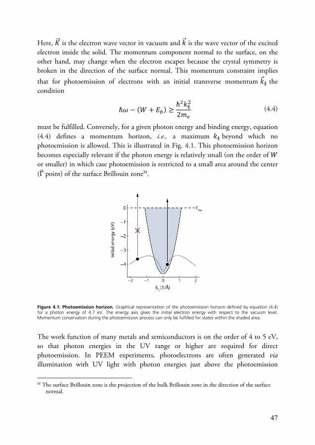
47
Here, 𝐾 is the electron wave vector in vacuum and 𝑘 is the wave vector of the excited electron inside the solid. The momentum component normal to the surface, on the other hand, may change when the electron escapes because the crystal symmetry is broken in the direction of the surface normal. This momentum constraint implies that for photoemission of electrons with an initial transverse momentum 𝑘∥ the condition
ℏ𝜔 − (𝑊 + 𝐸 ) ≥ ℏ 𝑘∥2𝑚 (4.4)
must be fulfilled. Conversely, for a given photon energy and binding energy, equation (4.4) defines a momentum horizon, i.e., a maximum 𝑘∥ beyond which no photoemission is allowed. This is illustrated in Fig. 4.1. This photoemission horizon becomes especially relevant if the photon energy is relatively small (on the order of 𝑊 or smaller) in which case photoemission is restricted to a small area around the center (Γ point) of the surface Brillouin zoneM.
Figure 4.1: Photoemission horizon. Graphical representation of the photoemission horizon defined by equation (4.4) for a photon energy of 4.7 eV. The energy axis gives the initial electron energy with respect to the vacuum level. Momentum conservation during the photoemission process can only be fulfilled for states within the shaded area.
The work function of many metals and semiconductors is on the order of 4 to 5 eV, so that photon energies in the UV range or higher are required for direct photoemission. In PEEM experiments, photoelectrons are often generated via illumination with UV light with photon energies just above the photoemission
M The surface Brillouin zone is the projection of the bulk Brillouin zone in the direction of the surface
normal.
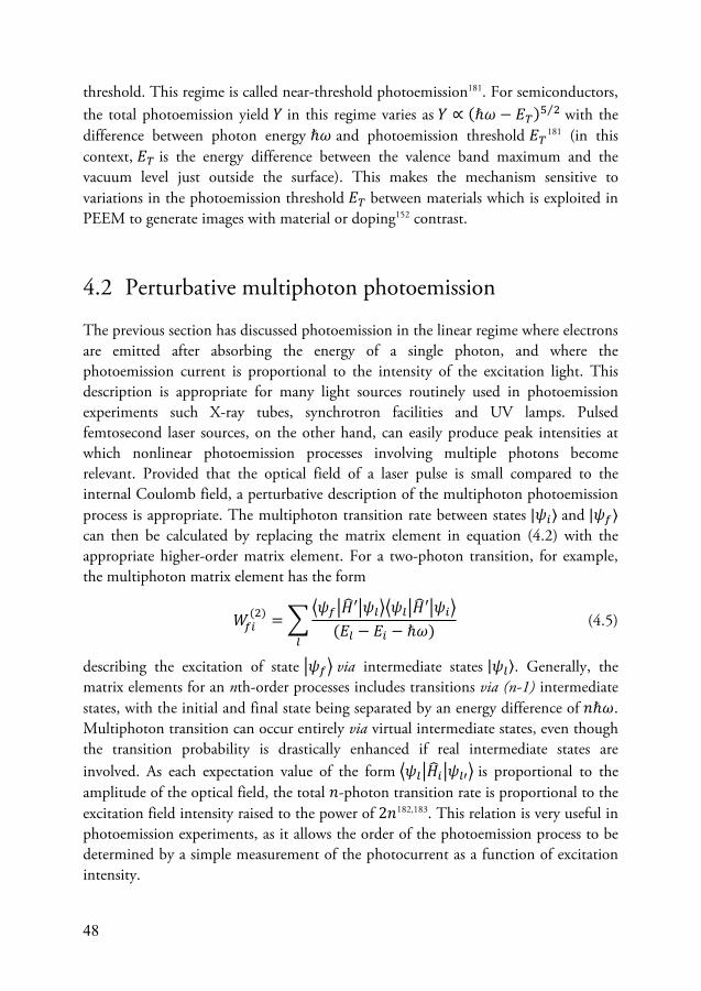
48
threshold. This regime is called near-threshold photoemission181. For semiconductors, the total photoemission yield 𝑌 in this regime varies as 𝑌 ∝ (ℏ𝜔 − 𝐸 ) ⁄ with the difference between photon energy ℏ𝜔 and photoemission threshold 𝐸 181 (in this context, 𝐸 is the energy difference between the valence band maximum and the vacuum level just outside the surface). This makes the mechanism sensitive to variations in the photoemission threshold 𝐸 between materials which is exploited in PEEM to generate images with material or doping152 contrast.
4.2 Perturbative multiphoton photoemission
The previous section has discussed photoemission in the linear regime where electrons are emitted after absorbing the energy of a single photon, and where the photoemission current is proportional to the intensity of the excitation light. This description is appropriate for many light sources routinely used in photoemission experiments such X-ray tubes, synchrotron facilities and UV lamps. Pulsed femtosecond laser sources, on the other hand, can easily produce peak intensities at which nonlinear photoemission processes involving multiple photons become relevant. Provided that the optical field of a laser pulse is small compared to the internal Coulomb field, a perturbative description of the multiphoton photoemission process is appropriate. The multiphoton transition rate between states |𝜓 ⟩ and |𝜓 ⟩ can then be calculated by replacing the matrix element in equation (4.2) with the appropriate higher-order matrix element. For a two-photon transition, for example, the multiphoton matrix element has the form 𝑊( ) = 𝜓 𝐻′ 𝜓 𝜓 𝐻′ 𝜓(𝐸 − 𝐸 − ℏ𝜔) (4.5)
describing the excitation of state 𝜓 via intermediate states |𝜓 ⟩. Generally, the matrix elements for an nth-order processes includes transitions via (n-1) intermediate states, with the initial and final state being separated by an energy difference of 𝑛ℏ𝜔. Multiphoton transition can occur entirely via virtual intermediate states, even though the transition probability is drastically enhanced if real intermediate states are involved. As each expectation value of the form 𝜓 𝐻 𝜓 is proportional to the amplitude of the optical field, the total 𝑛-photon transition rate is proportional to the excitation field intensity raised to the power of 2𝑛182,183. This relation is very useful in photoemission experiments, as it allows the order of the photoemission process to be determined by a simple measurement of the photocurrent as a function of excitation intensity.
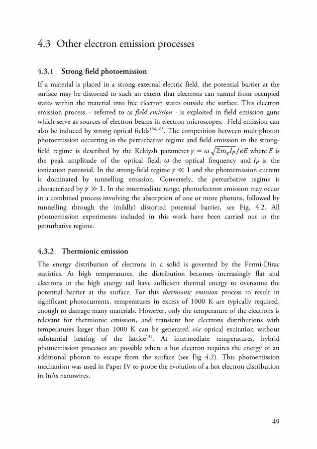
49
4.3 Other electron emission processes
4.3.1 Strong-field photoemission
If a material is placed in a strong external electric field, the potential barrier at the surface may be distorted to such an extent that electrons can tunnel from occupied states within the material into free electron states outside the surface. This electron emission process – referred to as field emission - is exploited in field emission guns which serve as sources of electron beams in electron microscopes. Field emission can also be induced by strong optical fields184,185. The competition between multiphoton photoemission occurring in the perturbative regime and field emission in the strong-field regime is described by the Keldysh parameter 𝛾 = 𝜔 2𝑚 𝐼 𝑒𝐸⁄ where 𝐸 is the peak amplitude of the optical field, 𝜔 the optical frequency and 𝐼 is the ionization potential. In the strong-field regime 𝛾 ≪ 1 and the photoemission current is dominated by tunnelling emission. Conversely, the perturbative regime is characterized by 𝛾 ≫ 1. In the intermediate range, photoelectron emission may occur in a combined process involving the absorption of one or more photons, followed by tunnelling through the (mildly) distorted potential barrier, see Fig. 4.2. All photoemission experiments included in this work have been carried out in the perturbative regime.
4.3.2 Thermionic emission
The energy distribution of electrons in a solid is governed by the Fermi-Dirac statistics. At high temperatures, the distribution becomes increasingly flat and electrons in the high energy tail have sufficient thermal energy to overcome the potential barrier at the surface. For this thermionic emission process to result in significant photocurrents, temperatures in excess of 1000 K are typically required, enough to damage many materials. However, only the temperature of the electrons is relevant for thermionic emission, and transient hot electrons distributions with temperatures larger than 1000 K can be generated via optical excitation without substantial heating of the lattice131. At intermediate temperatures, hybrid photoemission processes are possible where a hot electron requires the energy of an additional photon to escape from the surface (see Fig 4.2). This photoemission mechanism was used in Paper IV to probe the evolution of a hot electron distribution in InAs nanowires.
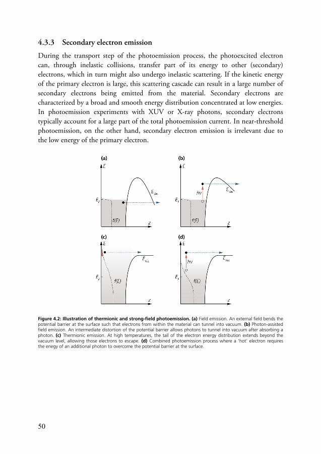
50
4.3.3 Secondary electron emission
During the transport step of the photoemission process, the photoexcited electron can, through inelastic collisions, transfer part of its energy to other (secondary) electrons, which in turn might also undergo inelastic scattering. If the kinetic energy of the primary electron is large, this scattering cascade can result in a large number of secondary electrons being emitted from the material. Secondary electrons are characterized by a broad and smooth energy distribution concentrated at low energies. In photoemission experiments with XUV or X-ray photons, secondary electrons typically account for a large part of the total photoemission current. In near-threshold photoemission, on the other hand, secondary electron emission is irrelevant due to the low energy of the primary electron.
Figure 4.2: Illustration of thermionic and strong-field photoemission. (a) Field emission. An external field bends the potential barrier at the surface such that electrons from within the material can tunnel into vacuum. (b) Photon-assisted field emission. An intermediate distortion of the potential barrier allows photons to tunnel into vacuum after absorbing a photon. (c) Thermionic emission. At high temperatures, the tail of the electron energy distribution extends beyond the vacuum level, allowing those electrons to escape. (d) Combined photoemission process where a ‘hot’ electron requires the enegy of an additional photon to overcome the potential barrier at the surface.
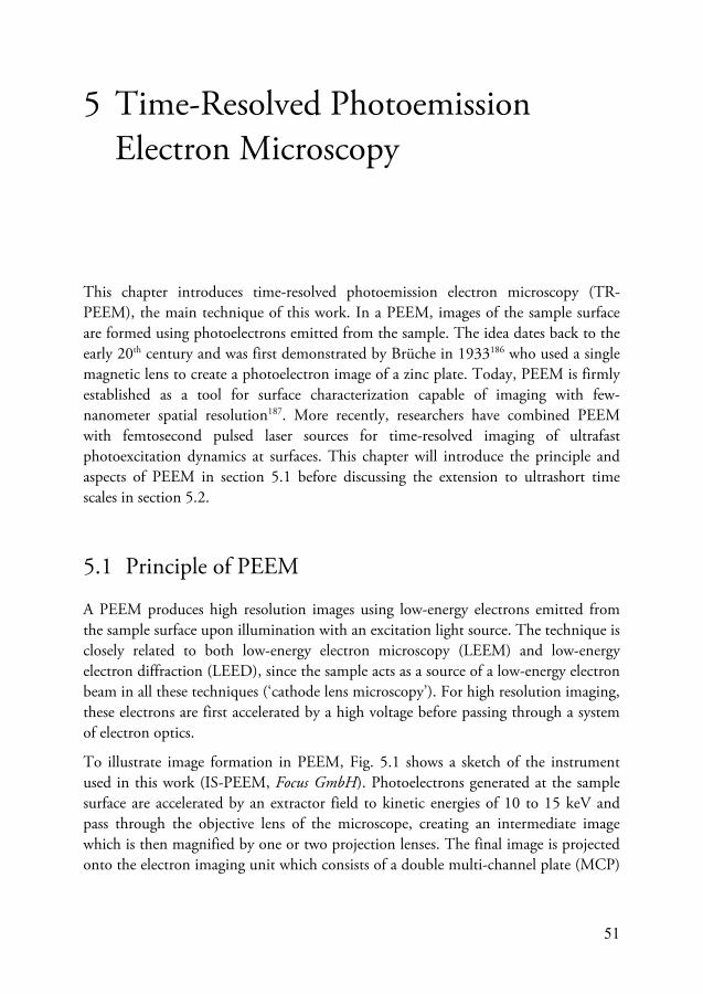
51
5 Time-Resolved Photoemission Electron Microscopy
This chapter introduces time-resolved photoemission electron microscopy (TR-PEEM), the main technique of this work. In a PEEM, images of the sample surface are formed using photoelectrons emitted from the sample. The idea dates back to the early 20th century and was first demonstrated by Brüche in 1933186 who used a single magnetic lens to create a photoelectron image of a zinc plate. Today, PEEM is firmly established as a tool for surface characterization capable of imaging with few-nanometer spatial resolution187. More recently, researchers have combined PEEM with femtosecond pulsed laser sources for time-resolved imaging of ultrafast photoexcitation dynamics at surfaces. This chapter will introduce the principle and aspects of PEEM in section 5.1 before discussing the extension to ultrashort time scales in section 5.2.
5.1 Principle of PEEM
A PEEM produces high resolution images using low-energy electrons emitted from the sample surface upon illumination with an excitation light source. The technique is closely related to both low-energy electron microscopy (LEEM) and low-energy electron diffraction (LEED), since the sample acts as a source of a low-energy electron beam in all these techniques (‘cathode lens microscopy’). For high resolution imaging, these electrons are first accelerated by a high voltage before passing through a system of electron optics.
To illustrate image formation in PEEM, Fig. 5.1 shows a sketch of the instrument used in this work (IS-PEEM, Focus GmbH). Photoelectrons generated at the sample surface are accelerated by an extractor field to kinetic energies of 10 to 15 keV and pass through the objective lens of the microscope, creating an intermediate image which is then magnified by one or two projection lenses. The final image is projected onto the electron imaging unit which consists of a double multi-channel plate (MCP)
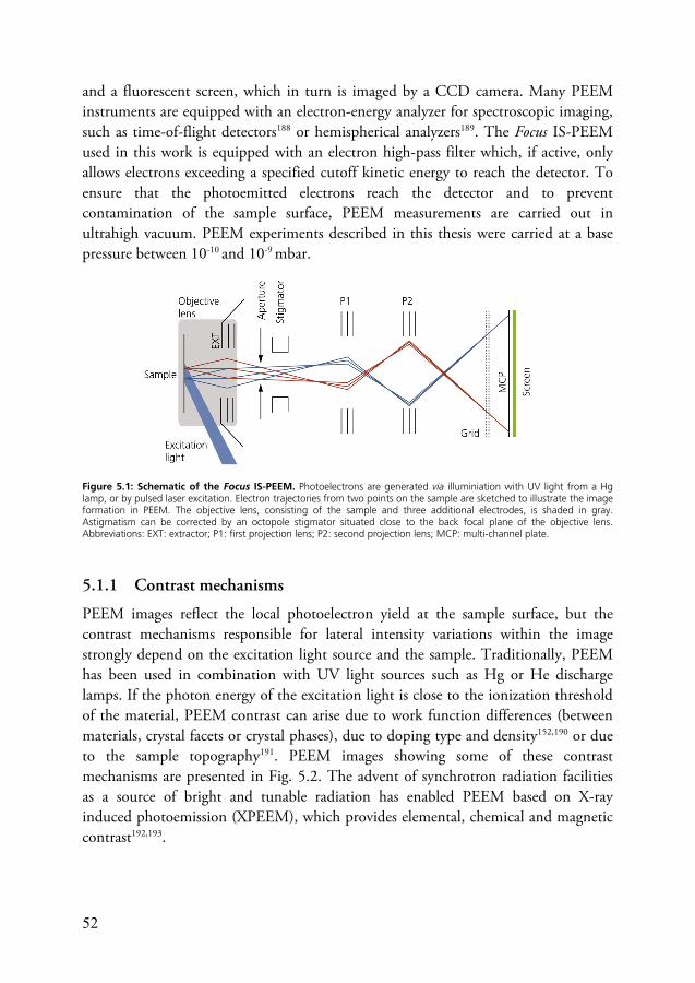
52
and a fluorescent screen, which in turn is imaged by a CCD camera. Many PEEM instruments are equipped with an electron-energy analyzer for spectroscopic imaging, such as time-of-flight detectors188 or hemispherical analyzers189. The Focus IS-PEEM used in this work is equipped with an electron high-pass filter which, if active, only allows electrons exceeding a specified cutoff kinetic energy to reach the detector. To ensure that the photoemitted electrons reach the detector and to prevent contamination of the sample surface, PEEM measurements are carried out in ultrahigh vacuum. PEEM experiments described in this thesis were carried at a base pressure between 10-10 and 10-9 mbar.
Figure 5.1: Schematic of the Focus IS-PEEM. Photoelectrons are generated via illuminiation with UV light from a Hg lamp, or by pulsed laser excitation. Electron trajectories from two points on the sample are sketched to illustrate the image formation in PEEM. The objective lens, consisting of the sample and three additional electrodes, is shaded in gray. Astigmatism can be corrected by an octopole stigmator situated close to the back focal plane of the objective lens. Abbreviations: EXT: extractor; P1: first projection lens; P2: second projection lens; MCP: multi-channel plate.
5.1.1 Contrast mechanisms
PEEM images reflect the local photoelectron yield at the sample surface, but the contrast mechanisms responsible for lateral intensity variations within the image strongly depend on the excitation light source and the sample. Traditionally, PEEM has been used in combination with UV light sources such as Hg or He discharge lamps. If the photon energy of the excitation light is close to the ionization threshold of the material, PEEM contrast can arise due to work function differences (between materials, crystal facets or crystal phases), due to doping type and density152,190 or due to the sample topography191. PEEM images showing some of these contrast mechanisms are presented in Fig. 5.2. The advent of synchrotron radiation facilities as a source of bright and tunable radiation has enabled PEEM based on X-ray induced photoemission (XPEEM), which provides elemental, chemical and magnetic contrast192,193.
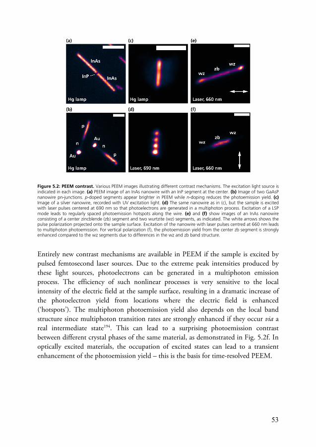
53
Figure 5.2: PEEM contrast. Various PEEM images illustrating different contrast mechanisms. The excitation light source is indicated in each image. (a) PEEM image of an InAs nanowire with an InP segment at the center. (b) Image of two GaAsP nanowire pn-junctions. p-doped segments appear brighter in PEEM while n-doping reduces the photoemission yield. (c) Image of a silver nanowire, recorded with UV excitation light. (d) The same nanowire as in (c), but the sample is excited with laser pulses centered at 690 nm so that photoelectrons are generated in a multiphoton process. Excitation of a LSP mode leads to regularly spaced photoemission hotspots along the wire. (e) and (f) show images of an InAs nanowire consisting of a center zincblende (zb) segment and two wurtzite (wz) segments, as indicated. The white arrows shows the pulse polarization projected onto the sample surface. Excitation of the nanowire with laser pulses centred at 660 nm leads to multiphoton photoemission. For vertical polarization (f), the photoemission yield from the center zb segment is strongly enhanced compared to the wz segments due to differences in the wz and zb band structure.
Entirely new contrast mechanisms are available in PEEM if the sample is excited by pulsed femtosecond laser sources. Due to the extreme peak intensities produced by these light sources, photoelectrons can be generated in a multiphoton emission process. The efficiency of such nonlinear processes is very sensitive to the local intensity of the electric field at the sample surface, resulting in a dramatic increase of the photoelectron yield from locations where the electric field is enhanced (‘hotspots’). The multiphoton photoemission yield also depends on the local band structure since multiphoton transition rates are strongly enhanced if they occur via a real intermediate state194. This can lead to a surprising photoemission contrast between different crystal phases of the same material, as demonstrated in Fig. 5.2f. In optically excited materials, the occupation of excited states can lead to a transient enhancement of the photoemission yield – this is the basis for time-resolved PEEM.

54
5.1.2 Spatial resolution
The spatial resolution of PEEM is ultimately limited by diffraction effects. Photoelectrons emitted with a kinetic energy of ~1 eV have a wavelength on the order of ~1 nm, such that imaging with a resolution better than 1 nm is fundamentally possible at these energies. In practice, however, the spatial resolution of the Focus IS-PEEM is limited to ~40 nm due to aberrations introduced by the objective lens of the microscope. The Focus IS-PEEM includes an electrostatic tetrode objective lens consisting of four electrodes, arranged as shown in the sketch in Fig. 5.3b. Notably, one of these electrodes is the sample itself which is thus an integral part of the electron optics. In a first approximation, the objective lens can be divided into an acceleration field, defined by the potential difference between the sample and the extractor electrode, and a focusing part195, as indicated in Fig. 5.3b, with both parts contributing to the total aberration of the lens. To minimize the aberrations introduced by the acceleration field, it must be as homogeneous and stable as possible. This implies that the sample has to be flat, (semi-) conductive, and precisely aligned with respect to the axis of the microscope to achieve the optimum resolution.
As a result of diffraction and aberrations, photoelectrons emitted from a single point on the sample will be imaged as a disc with radius 𝑟 = 𝑟 + 𝑟 + 𝑟 (5.1)
where 𝑟 and 𝑟 describe the effect of the spherical and chromatic aberration of the (entire) objective lens while 𝑟 describes diffraction effects. These contributions are given by: 𝑟 ≈ 0.73 nm𝐸 /𝑒𝑉 sin 𝛼 (5.2)
𝑟 ≈ 14 𝑙 𝐸𝐸 + 𝐶 𝐸𝐸 𝛼 (5.3)
𝑟 ≈ 𝑙 𝐸𝐸 + 𝐶 𝐸𝐸 Δ𝐸𝐸 𝛼 (5.4)
Here, 𝐸 is the starting energy of the photoelectrons, 𝐸 is the energy after acceleration by the extractor field, 𝛼 is the emission angle, 𝑙 is the sample-extractor distance and Δ𝐸 is the energy spread of the emitted electrons. 𝐶 and 𝐶 are the

55
spherical and chromatic aberration coefficients of the objective lens. In order to achieve the best possible spatial resolution, it is thus necessary to
(i) Use a high extractor voltage so that the ratio 𝐸 /𝐸 remains small.
(ii) Image electrons with small starting angle 𝛼 .
(iii) Ensure a small energy spread of the photoemitted electrons.
The energy spread Δ𝐸 can in principle be controlled if the PEEM is equipped with an energy filter. However, the PEEM instrument used in this work was usually operated in energy-integrated mode in which case the relative energy spread is determined by the properties of the excitation light and its interaction with the sample. A contrast aperture placed in the back focal plane of the objective lens can be used to block electrons that are emitted with large starting angles 𝛼 . In the Focus IS-PEEM, contrast apertures with diameters ranging from 30 μm to 1.5 mm are available. While a small aperture is required to achieve the best possible spatial resolution, it also severely reduces the fraction of photoelectrons reaching the detector. For example, at a starting energy of 1 eV and a cosine distribution of the starting angles, a 500 μm aperture results in a microscope transmission of 100% while the 30 μm aperture only permits 2% of the photoelectrons to reach the detector.
Figure 5.3: Spatial resolution of PEEM. (a) Radius of the resolution disk in PEEM for typical imaging conditions using a UV-discharge lamp as excitation source. The individual contributions from diffraction, spherical and chromatic aberration are shown. The maximum starting angles corresponding to different contrast aperture diameters, as marked. Aberration coefficients 𝐶 = 300 mm and 𝐶 = 130 mm and a sample-extractor distance of 1.8 mm were assumed, as appropriate for the Focus IS-PEEM. (b) Sketch of a tetrode objective lens, adapted from3. The lens consists of four electrodes, sample (SPL), extractor (EXT), focus (FOC) and column (COL). Typical potential differences between the electrodes and the sample (ground) are indicated. The electrons are accelerated between SPL and EXT. For the voltages given here, focusing occurs mostly between the EXT and the FOC electrode.
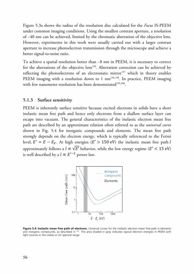
56
Figure 5.3a shows the radius of the resolution disc calculated for the Focus IS-PEEM under common imaging conditions. Using the smallest contrast aperture, a resolution of ~40 nm can be achieved, limited by the chromatic aberration of the objective lens. However, experiments in this work were usually carried out with a larger contrast aperture to increase photoelectron transmission through the microscope and achieve a better signal-to-noise ratio.
To achieve a spatial resolution better than ~8 nm in PEEM, it is necessary to correct for the aberrations of the objective lens196. Aberration correction can be achieved by reflecting the photoelectrons of an electrostatic mirror197 which in theory enables PEEM imaging with a resolution down to 1 nm196,198. In practice, PEEM imaging with few nanometer resolution has been demonstrated199,200.
5.1.3 Surface sensitivity
PEEM is inherently surface sensitive because excited electrons in solids have a short inelastic mean free path and hence only electrons from a shallow surface layer can escape into vacuum. The general characteristics of the inelastic electron mean free path are described by an approximate relation often referred to as the universal curve shown in Fig. 5.4 for inorganic compounds and elements. The mean free path strongly depends on the electron energy, which is typically referenced to the Fermi level, 𝐸 = 𝐸 − 𝐸 . At high energies (𝐸′ > 150 eV) the inelastic mean free path 𝑙 approximately follows a 𝑙 ∝ √𝐸′ behavior, while the low energy regime (𝐸′ < 15 eV) is well described by a 𝑙 ∝ 𝐸′ power law.
Figure 5.4: Inelastic mean free path of electrons. Universal curves for the inelastic electron mean free path in elements and inorganic compounds, as described in 201. The area shaded in gray indicates typical electron energies in PEEM with light sources in the visible or UV spectral range.
57
The minimum mean free path is found in the transition region at energies around 50 to 100 eV. At its minimum, the mean free path corresponds to a single monolayer or less, such that the majority of the primary photoelectrons originates in the topmost atomic layer of the sample, allowing for extremely surface sensitive measurements. It should be noted that while the universal curve captures the general characteristics of the inelastic mean free path, the values for specific materials might show significant deviation from the curve.
PEEM can be operated with a wide range of light sources at photon energies ranging from the near-infrared to the hard X-ray range, and the electron mean free path varies accordingly. In this work, PEEM experiments were carried out using light sources of relatively low photon energies below 5 eV, which results in excited electrons with energies of a few eV with respect to the Fermi level. This energy range, which is highlighted in Fig. 5.4, corresponds the values of 𝑙 ranging from a few nanometers to around 10 nm, implying that PEEM experiments in these conditions are still mostly sensitive to surface-related phenomena.
5.2 Time-resolved PEEM
In conventional PEEM, as well as in other electron microscopy techniques, the imaging speed is limited to video rates. In TR-PEEM, this limitation is circumvented by using femtosecond laser pulses as excitation light source, making it possible to time excitation and imaging of the sample with femtosecond accuracy. In comparison to other ultrafast electron microscopy techniques such as ultrafast transmission electron microscopy (UTEM)1 or ultrafast scanning electron microscopy (USEM)202, TR-PEEM benefits from the fact that generation and control of short electron wave packets is not required. As a consequence, it is comparatively easy to reach time-resolutions better than 10 fs in TR-PEEM19 and several groups are working towards imaging with attosecond resolution203,204.
PEEM imaging with femtosecond laser pulses in the visible or near-infrared spectral range is highly sensitive to optical near-fields at surfaces. The technique has thus been used extensively to study localized and propagating surface plasmon polaritons at noble metal surfaces, with pioneering experiments carried out by Schmidt et al.16 and Kubo et al.17 in the early 2000s. PEEM experiments on plasmonic systems are almost exclusively based on an approach called interferometric time-resolved PEEM (ITR-PEEM) where the spatiotemporal properties of plasmonic resonances are derived from
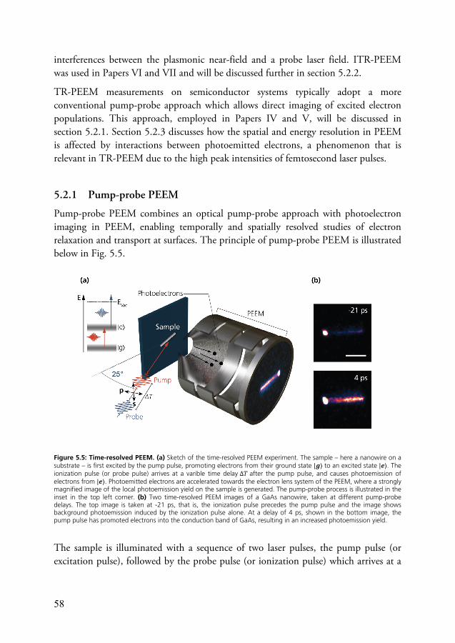
58
interferences between the plasmonic near-field and a probe laser field. ITR-PEEM was used in Papers VI and VII and will be discussed further in section 5.2.2.
TR-PEEM measurements on semiconductor systems typically adopt a more conventional pump-probe approach which allows direct imaging of excited electron populations. This approach, employed in Papers IV and V, will be discussed in section 5.2.1. Section 5.2.3 discusses how the spatial and energy resolution in PEEM is affected by interactions between photoemitted electrons, a phenomenon that is relevant in TR-PEEM due to the high peak intensities of femtosecond laser pulses.
5.2.1 Pump-probe PEEM
Pump-probe PEEM combines an optical pump-probe approach with photoelectron imaging in PEEM, enabling temporally and spatially resolved studies of electron relaxation and transport at surfaces. The principle of pump-probe PEEM is illustrated below in Fig. 5.5.
Figure 5.5: Time-resolved PEEM. (a) Sketch of the time-resolved PEEM experiment. The sample – here a nanowire on a substrate – is first excited by the pump pulse, promoting electrons from their ground state |𝒈⟩ to an excited state |𝒆⟩. The ionization pulse (or probe pulse) arrives at a varible time delay Δ𝑇 after the pump pulse, and causes photoemission of electrons from |𝒆⟩. Photoemitted electrons are accelerated towards the electron lens system of the PEEM, where a strongly magnified image of the local photoemission yield on the sample is generated. The pump-probe process is illustrated in the inset in the top left corner. (b) Two time-resolved PEEM images of a GaAs nanowire, taken at different pump-probe delays. The top image is taken at -21 ps, that is, the ionization pulse precedes the pump pulse and the image shows background photoemission induced by the ionization pulse alone. At a delay of 4 ps, shown in the bottom image, the pump pulse has promoted electrons into the conduction band of GaAs, resulting in an increased photoemission yield.
The sample is illuminated with a sequence of two laser pulses, the pump pulse (or excitation pulse), followed by the probe pulse (or ionization pulse) which arrives at a
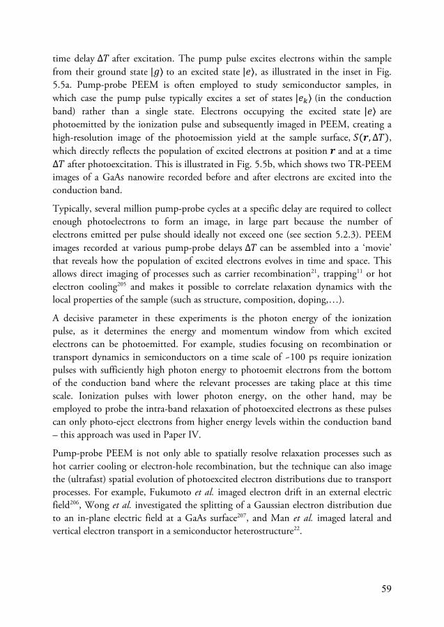
59
time delay Δ𝑇 after excitation. The pump pulse excites electrons within the sample from their ground state |𝑔⟩ to an excited state |𝑒⟩, as illustrated in the inset in Fig. 5.5a. Pump-probe PEEM is often employed to study semiconductor samples, in which case the pump pulse typically excites a set of states |𝑒 ⟩ (in the conduction band) rather than a single state. Electrons occupying the excited state |𝑒⟩ are photoemitted by the ionization pulse and subsequently imaged in PEEM, creating a high-resolution image of the photoemission yield at the sample surface, 𝑆(𝒓, Δ𝑇), which directly reflects the population of excited electrons at position 𝒓 and at a time Δ𝑇 after photoexcitation. This is illustrated in Fig. 5.5b, which shows two TR-PEEM images of a GaAs nanowire recorded before and after electrons are excited into the conduction band.
Typically, several million pump-probe cycles at a specific delay are required to collect enough photoelectrons to form an image, in large part because the number of electrons emitted per pulse should ideally not exceed one (see section 5.2.3). PEEM images recorded at various pump-probe delays Δ𝑇 can be assembled into a ‘movie’ that reveals how the population of excited electrons evolves in time and space. This allows direct imaging of processes such as carrier recombination21, trapping11 or hot electron cooling205 and makes it possible to correlate relaxation dynamics with the local properties of the sample (such as structure, composition, doping,…).
A decisive parameter in these experiments is the photon energy of the ionization pulse, as it determines the energy and momentum window from which excited electrons can be photoemitted. For example, studies focusing on recombination or transport dynamics in semiconductors on a time scale of ~100 ps require ionization pulses with sufficiently high photon energy to photoemit electrons from the bottom of the conduction band where the relevant processes are taking place at this time scale. Ionization pulses with lower photon energy, on the other hand, may be employed to probe the intra-band relaxation of photoexcited electrons as these pulses can only photo-eject electrons from higher energy levels within the conduction band – this approach was used in Paper IV.
Pump-probe PEEM is not only able to spatially resolve relaxation processes such as hot carrier cooling or electron-hole recombination, but the technique can also image the (ultrafast) spatial evolution of photoexcited electron distributions due to transport processes. For example, Fukumoto et al. imaged electron drift in an external electric field206, Wong et al. investigated the splitting of a Gaussian electron distribution due to an in-plane electric field at a GaAs surface207, and Man et al. imaged lateral and vertical electron transport in a semiconductor heterostructure22.
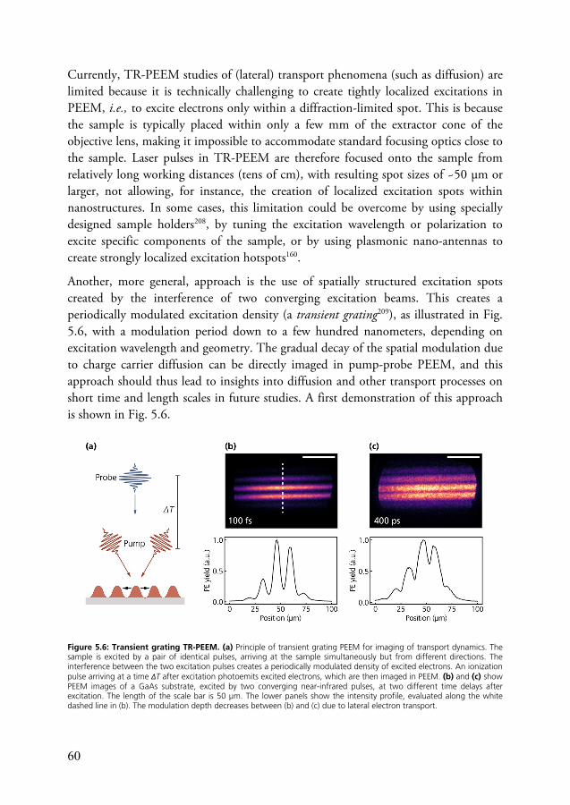
60
Currently, TR-PEEM studies of (lateral) transport phenomena (such as diffusion) are limited because it is technically challenging to create tightly localized excitations in PEEM, i.e., to excite electrons only within a diffraction-limited spot. This is because the sample is typically placed within only a few mm of the extractor cone of the objective lens, making it impossible to accommodate standard focusing optics close to the sample. Laser pulses in TR-PEEM are therefore focused onto the sample from relatively long working distances (tens of cm), with resulting spot sizes of ~50 μm or larger, not allowing, for instance, the creation of localized excitation spots within nanostructures. In some cases, this limitation could be overcome by using specially designed sample holders208, by tuning the excitation wavelength or polarization to excite specific components of the sample, or by using plasmonic nano-antennas to create strongly localized excitation hotspots160.
Another, more general, approach is the use of spatially structured excitation spots created by the interference of two converging excitation beams. This creates a periodically modulated excitation density (a transient grating209), as illustrated in Fig. 5.6, with a modulation period down to a few hundred nanometers, depending on excitation wavelength and geometry. The gradual decay of the spatial modulation due to charge carrier diffusion can be directly imaged in pump-probe PEEM, and this approach should thus lead to insights into diffusion and other transport processes on short time and length scales in future studies. A first demonstration of this approach is shown in Fig. 5.6.
Figure 5.6: Transient grating TR-PEEM. (a) Principle of transient grating PEEM for imaging of transport dynamics. The sample is excited by a pair of identical pulses, arriving at the sample simultaneously but from different directions. The interference between the two excitation pulses creates a periodically modulated density of excited electrons. An ionization pulse arriving at a time ΔT after excitation photoemits excited electrons, which are then imaged in PEEM. (b) and (c) show PEEM images of a GaAs substrate, excited by two converging near-infrared pulses, at two different time delays after excitation. The length of the scale bar is 50 μm. The lower panels show the intensity profile, evaluated along the white dashed line in (b). The modulation depth decreases between (b) and (c) due to lateral electron transport.

61
In addition to lateral electron transport (parallel to the sample surface) TR-PEEM is also able to probe vertical electron transport, i.e., transport of electrons from the interior of the sample towards the surface or vice versa. This is related to the surface sensitivity of PEEM. Since all photoelectrons originate from a thin surface layer, accumulation or depletion of electrons near the sample surface due to transport will appear as a rise or decay of the photoemission signal. This is a common phenomenon at semiconductor surfaces where band bending can drive photoexcited electrons towards or away from the surface (see section 3.2).
Interpretation of TR-PEEM experiments can be challenging since various ultrafast processes can contribute to changes in the total photoelectron yield from a given position on the sample. For example, most TR-PEEM studies on semiconductors rely on UV ionization pulse with photon energies around ~4.5 eV to probe the population of excited electrons in the conduction band around the center of the Brillouin zone. Such an experiment probes the electronic population within a specific energy range, within a limited region in reciprocal space (see chapter 4), and within a limited region in real space (due to the surface sensitivity of PEEM). Correspondingly, a decay in photoemission yield could be attributed to energy relaxation (recombination), to electrons scattering to conduction band side valleys beyond the photoemission horizon of the probe pulse, or to electron transport away from the sample surface. In some cases, this ambiguity can be lifted based on the observed decay rates since the general time scales for many relaxation processes are well established in the literature, especially for thoroughly studied materials such as GaAs or other III-V compounds.
The excitation fluence dependence of the photoemission yield evolution also provides valuable clues, as many relaxation processes show a characteristic dependence on the density of excited electrons. Recombination rates due to mono-molecular, bi-molecular, or Auger recombination, for instance, can be identified based on the excitation density dependence of the decay dynamics210. Likewise, hot carrier cooling due to carrier-carrier scattering or electron-phonon scattering can be distinguished based on the density dependence of these scattering mechanisms. To allow a more detailed view of the relaxation dynamics, the emitted photoelectrons are often resolved in energy in TR-PEEM experiments. This provides insight into the energy distribution of the excited electrons within the sample, which is very valuable in studies of hot electron cooling211.
Another way to extend the ‘standard’ pump-probe TR-PEEM approach and access additional spectral information is the combination of TR-PEEM with optical Fourier transform spectroscopy. In Paper V, for example, we demonstrate TR-PEEM with excitation frequency resolution by incorporating one-dimensional Fourier transform spectroscopy. A more detailed description of the approach and the results of Paper V
62
is provided in chapter 6. In fact, even highly complex optical spectroscopy techniques can be combined with PEEM for spectroscopic imaging with nanoscale resolution, provided that the spectra can be recorded using an incoherent signalN such as photoelectron emission. Aeschlimann et al., for instance, combined PEEM with time-resolved 2D Fourier transform spectroscopy12,50, an advanced ultrafast spectroscopy technique often employed to explore electronic coupling and photoexcitation dynamics in complex molecular systems212. In combination with PEEM, the technique can provide a detailed view of the local electronic structure and shed light on processes such as dephasing or energy transfer, even though the recording of a sequence of transient 2D spectra in PEEM has so far not been demonstrated in the literature. While the spectral information available in these extended experimental schemes can be very valuable, they come at the cost of an increasingly complex experimental apparatus and substantially longer data acquisition times.
5.2.2 Interferometric time-resolved PEEM
PEEM in combination with femtosecond laser pulses has been intensely utilized in the study of localized and propagating surface plasmon polaritons17,19,20,168,178,213. These experiments are almost exclusively based on an approach referred to as interferometric time-resolved PEEM (ITR-PEEM), which relies on multiphoton photoemission to investigate the spatiotemporal evolution of optical near-fields at surfaces.
The technique is illustrated in Fig. 5.7. The sample – here a metallic nanoparticle supporting LSP resonances – is illuminated by a pair of identical femtosecond laser pulses separated by a time delay τ which is controlled with sub-cycle accuracy. Each of the two pulses excites plasmonic resonances of the nanoparticle, resulting in an optical near-field 𝐸 (𝑟, 𝑡) at the sample surface whose spatial and temporal properties are characteristic of the excited LSP resonances. The total field induced by two time-delayed pulses is then obtained as the linear superposition of the contributions from the individual pulses: 𝐸 (𝑟, 𝑡, 𝜏) = 𝐸 (𝑟, 𝑡) + 𝐸 (𝑟, 𝑡 − 𝜏) (5.5)
ITR-PEEM experiments use excitation pulses with photon energies below the work function of the sample, such that photoelectrons can only be emitted in a multiphoton process, typically requiring 2 or 3 photons. In an ITR-PEEM experiment, the local multiphoton photoemission yield 𝑆(𝑟, 𝜏) is imaged as a
N Here, ‘incoherent signal’ refers to a signal without phase information, as opposed to, e.g., a coherently detected optical signal.
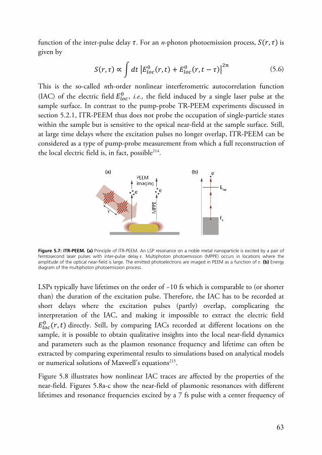
63
function of the inter-pulse delay 𝜏. For an n-photon photoemission process, 𝑆(𝑟, 𝜏) is given by
𝑆(𝑟, 𝜏) ∝ 𝑑𝑡 𝐸 (𝑟, 𝑡) + 𝐸 (𝑟, 𝑡 − 𝜏) (5.6)
This is the so-called nth-order nonlinear interferometric autocorrelation function (IAC) of the electric field 𝐸 , i.e., the field induced by a single laser pulse at the sample surface. In contrast to the pump-probe TR-PEEM experiments discussed in section 5.2.1, ITR-PEEM thus does not probe the occupation of single-particle states within the sample but is sensitive to the optical near-field at the sample surface. Still, at large time delays where the excitation pulses no longer overlap, ITR-PEEM can be considered as a type of pump-probe measurement from which a full reconstruction of the local electric field is, in fact, possible214.
Figure 5.7: ITR-PEEM. (a) Principle of ITR-PEEM. An LSP resonance on a noble metal nanoparticle is excited by a pair of femtosecond laser pulses with inter-pulse delay 𝜏. Multiphoton photoemission (MPPE) occurs in locations where the amplitude of the optical near-field is large. The emitted photoelectrons are imaged in PEEM as a function of 𝜏. (b) Energy diagram of the multiphoton photoemission process.
LSPs typically have lifetimes on the order of ~10 fs which is comparable to (or shorter than) the duration of the excitation pulse. Therefore, the IAC has to be recorded at short delays where the excitation pulses (partly) overlap, complicating the interpretation of the IAC, and making it impossible to extract the electric field 𝐸 (𝑟, 𝑡) directly. Still, by comparing IACs recorded at different locations on the sample, it is possible to obtain qualitative insights into the local near-field dynamics and parameters such as the plasmon resonance frequency and lifetime can often be extracted by comparing experimental results to simulations based on analytical models or numerical solutions of Maxwell’s equations215.
Figure 5.8 illustrates how nonlinear IAC traces are affected by the properties of the near-field. Figures 5.8a-c show the near-field of plasmonic resonances with different lifetimes and resonance frequencies excited by a 7 fs pulse with a center frequency of
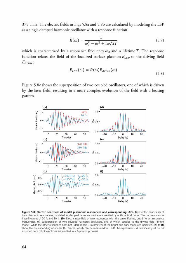
64
375 THz. The electric fields in Figs 5.8a and 5.8b are calculated by modeling the LSP as a single damped harmonic oscillator with a response function
𝑅(𝜔) = 1𝜔 − 𝜔 + 𝑖𝜔 2𝑇⁄ (5.7)
which is characterized by a resonance frequency 𝜔 and a lifetime 𝑇. The response function relates the field of the localized surface plasmon 𝐸 to the driving field 𝐸 :
𝐸 (𝜔) = 𝑅(𝜔)𝐸 (𝜔)
(5.8)
Figure 5.8c shows the superposition of two coupled oscillators, one of which is driven by the laser field, resulting in a more complex evolution of the field with a beating pattern.
Figure 5.8: Electric near-field of model plasmonic resonances and corresponding IACs. (a) Electric near-fields of two plasmonic resonances, modeled as damped harmonic oscillators, excited by a 7fs optical pulse. The two resonances have lifetimes of 20 fs and 30 fs. (b) Electric near-field of two resonances with the same lifetime, but different resonance frequencies. (c) Superposition of two coupled harmonic oscillators, one of which couples to the driving field (‘bright mode’) while the other resonance does not (‘dark mode’). Parameters of the bright and dark mode are indicated. (d) to (f) show the corresponding nonlinear IAC traces, which can be measured in ITR-PEEM experiments. A nonlinearity of n=3 is assumed here (photoelectrons are emitted in a 3-photon process).
65
Despite the simplicity of these models, LSP resonances in simple systems can often be successfully described in terms of a single or a few harmonic oscillators. IACs of the electric fields in Figs. 5.8a to 5.8c are shown in Figs. 5.8e to 5.8f for a nonlinearity n=3. Not surprisingly, a slower decay of the electric field amplitude also leads to a slower decay of the IAC, while a difference in resonance frequency results in a shift of the IAC maxima (Fig. 5.8e). Beating patterns, as visible in the IAC in Fig. 5.8f, indicate that two or more resonances of different frequencies contribute to the electric near-field.
ITR-PEEM is not only useful in studying LSP modes but has also been very successfully applied to investigate propagating SPPs on noble metal surfaces. Propagating plasmon modes typically have much longer lifetimes (few hundreds of fs), which allows ITR-PEEM experiments where the two excitation pulses are well-separated in time. The experiment then takes on a pump-probe character where the first pulse launches a propagating SPP, while the second pulse images the electric near-field at a variable time delay. Contrast is provided by an increase in the multiphoton photoemission yield due to constructive interference between the plasmon field and the probe pulse. In PEEM setups with normal-incidence illumination, this allows for direct imaging of propagating electromagnetic fields at surfaces18. For grazing incidence illumination (as in Paper VII), the interpretation of the PEEM images becomes slightly more complicated since the apparent plasmon wavelength becomes a function of the plasmon propagation direction18.
5.2.3 Space charge effects
In PEEM experiments using intense excitation light sources, the density of photoelectrons in the imaging column of the PEEM can become high enough for the Coulomb interaction between the propagating electrons to become relevant. In particular in PEEM experiments using amplified femtosecond laser pulses, the high peak intensity can easily lead to the generation of many photoelectrons by a single laser pulse, resulting in a bunch of electrons propagating through the imaging system in close proximity to each other. The Coulomb interaction between these electrons – referred to as space charge effects – leads to image blurring and loss of energy resolution216–218. This is illustrated in Fig. 5.9, which shows two PEEM images of GaAs nanowires recorded with different numbers of photoelectrons emitted per pulse.
The Coulomb interaction of the photoelectrons is typically divided into two contributions: deterministic space charge effects and stochastic Coulomb interactions217,219. The former can be seen as the interaction of each electron with an effective background charge density due to the presence of other electrons. If this
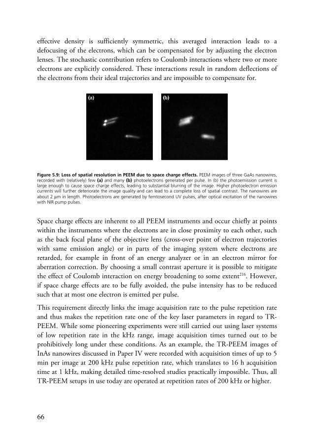
66
effective density is sufficiently symmetric, this averaged interaction leads to a defocusing of the electrons, which can be compensated for by adjusting the electron lenses. The stochastic contribution refers to Coulomb interactions where two or more electrons are explicitly considered. These interactions result in random deflections of the electrons from their ideal trajectories and are impossible to compensate for.
Figure 5.9: Loss of spatial resolution in PEEM due to space charge effects. PEEM images of three GaAs nanowires, recorded with (relatively) few (a) and many (b) photoelectrons generated per pulse. In (b) the photoemission current is large enough to cause space charge effects, leading to substantial blurring of the image. Higher photoelectron emission currents will further deteriorate the image quality and can lead to a complete loss of spatial contrast. The nanowires are about 2 μm in length. Photoelectrons are generated by femtosecond UV pulses, after optical excitation of the nanowires with NIR pump pulses.
Space charge effects are inherent to all PEEM instruments and occur chiefly at points within the instruments where the electrons are in close proximity to each other, such as the back focal plane of the objective lens (cross-over point of electron trajectories with same emission angle) or in parts of the imaging system where electrons are retarded, for example in front of an energy analyzer or in an electron mirror for aberration correction. By choosing a small contrast aperture it is possible to mitigate the effect of Coulomb interaction on energy broadening to some extent216. However, if space charge effects are to be fully avoided, the pulse intensity has to be reduced such that at most one electron is emitted per pulse.
This requirement directly links the image acquisition rate to the pulse repetition rate and thus makes the repetition rate one of the key laser parameters in regard to TR-PEEM. While some pioneering experiments were still carried out using laser systems of low repetition rate in the kHz range, image acquisition times turned out to be prohibitively long under these conditions. As an example, the TR-PEEM images of InAs nanowires discussed in Paper IV were recorded with acquisition times of up to 5 min per image at 200 kHz pulse repetition rate, which translates to 16 h acquisition time at 1 kHz, making detailed time-resolved studies practically impossible. Thus, all TR-PEEM setups in use today are operated at repetition rates of 200 kHz or higher.
67
6 Summary of Results
This chapter introduces the papers included in this work and provides a brief summary of the main results of each study. As mentioned in the introduction, the work behind this thesis follows two main lines: first, technical developments of the laser setup used for many of the TR-PEEM measurements carried out during my PhD studies. The main results of these efforts can be found in Papers I, II and III, and a summary is given in section 6.1. The second focus of this work was the application of TR-PEEM to investigate photoexcitation dynamics in nanostructures and at surfaces, represented by Papers IV to VII. These results are briefly summarized and discussed in section 6.2.
6.1 Developments in Ultrafast Optics
Several of the TR-PEEM experiments I was involved in - including those presented in Papers IV and V - were carried out using a laser setup initially designed for time-resolved 2D electronic spectroscopy. While only small adjustments were made for the initial, exploratory TR-PEEM experiments, several adjustments and extensions were introduced later to enable a broader range of time-resolved experiments in combination with PEEM. Figure 6.1 provides an overview of the setup in its state at the time of writing this thesis.
The optical setup is based on a Yb:KGW laser system (Pharos, Light Conversion) producing amplified laser pulses at a wavelength of 1030 nm, with pulse energies of ~30 μJ at a pulse repetition rate of 200 kHz. The pulse duration is around 170 fs. A 50/50 beam splitter divides the output pulses from the Pharos laser. Each half is used to pump a NOPA, each of which generates broadband pulses with ~10 fs pulse duration, tunable through the visible and near-infrared spectral range, with pulse energies of up to 250 nJ. The output from NOPA I (lab-built) is guided through a transmission grating-based interferometer (Paper II), generating phase-locked pulse pairs for interferometric measurements before being guided to the PEEM vacuum chamber. The arrival time of the pulses is adjusted by a magnetic-drive translation
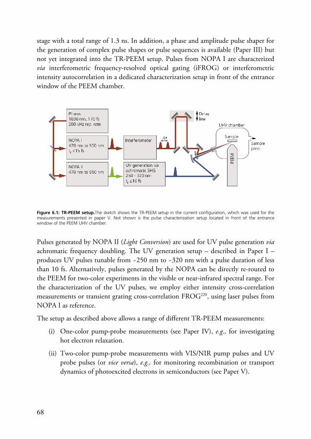
68
stage with a total range of 1.3 ns. In addition, a phase and amplitude pulse shaper for the generation of complex pulse shapes or pulse sequences is available (Paper III) but not yet integrated into the TR-PEEM setup. Pulses from NOPA I are characterized via interferometric frequency-resolved optical gating (iFROG) or interferometric intensity autocorrelation in a dedicated characterization setup in front of the entrance window of the PEEM chamber.
Figure 6.1: TR-PEEM setup.The sketch shows the TR-PEEM setup in the current configuration, which was used for the measurements presented in paper V. Not shown is the pulse characterization setup located in front of the entrance window of the PEEM UHV chamber.
Pulses generated by NOPA II (Light Conversion) are used for UV pulse generation via achromatic frequency doubling. The UV generation setup – described in Paper I – produces UV pulses tunable from ~250 nm to ~320 nm with a pulse duration of less than 10 fs. Alternatively, pulses generated by the NOPA can be directly re-routed to the PEEM for two-color experiments in the visible or near-infrared spectral range. For the characterization of the UV pulses, we employ either intensity cross-correlation measurements or transient grating cross-correlation FROG220, using laser pulses from NOPA I as reference.
The setup as described above allows a range of different TR-PEEM measurements:
(i) One-color pump-probe measurements (see Paper IV), e.g., for investigatinghot electron relaxation.
(ii) Two-color pump-probe measurements with VIS/NIR pump pulses and UVprobe pulses (or vice versa), e.g., for monitoring recombination or transportdynamics of photoexcited electrons in semiconductors (see Paper V).
69
(iii) Interferometric time-resolved PEEM to the study propagating and localized surface plasmon polaritons (as in Papers VI and VII).
(iv) Time-domain spectroscopy pump-probe measurements for the study of excitation-energy dependent carrier dynamics, as described in Paper V.
(v) After incorporation of the pulse shaper, further experiments are possible. For example, coherent control measurements or multidimensional Fourier-transform spectroscopy (‘2D-nanoscopy’)50,199.
The experiments described in Papers VI and VII are based on a different laser source described in detail elsewhere65. The setup is designed to generate attosecond XUV pulses via high harmonic generation at high repetition rates for various photoemission experiments, including PEEM221. The laser system generates spectrally broad few-cycle laser pulses shorter than 6 fs, well-suited for the study of short-lived LSP resonances.
6.1.1 Generation of UV pulses via achromatic phase-matching
TR-PEEM experiments probing the charge carrier dynamics around the Fermi level require UV ionization pulses with photon energies around 5 eV to overcome the work function (electron affinity) of many materials. Additionally, TR-PEEM requires laser systems operating at high pulse repetition rates (~100 kHz or more) to achieve reasonable measurement durations while avoiding space charge effects. Nowadays, the generation of such UV pulses is straightforward as frequency mixing processes in nonlinear crystals provide a direct route to generate laser pulses at the required energies. For example, frequency tripling or quadrupling of pulses at 800 nm (1.55 eV), as generated by the widely used Ti:Sapphire laser systems, can be readily accomplished and yields UV pulses at ~4.7 eV and ~6.2 eV, respectively, often used in time-resolved photoemission experiments11.
However, to achieve efficient frequency conversion over a large bandwidth necessary for pulses in the ~10 fs range, extremely thin nonlinear crystals are required. This, in turn, strongly reduces the overall efficiency of the process61 and complicates the generation of broad UV pulses at high repetition rates where pulse energies are typically low. Several alternative schemes for the generation of broad UV pulses have been demonstrated, such as up-conversion in noble gasses222 or nonlinear spectral broadening in hollow-core fibres223,224. These approaches, again, require high pulse energies and are therefore not applicable in combination with regular high-repetition rate laser systems.
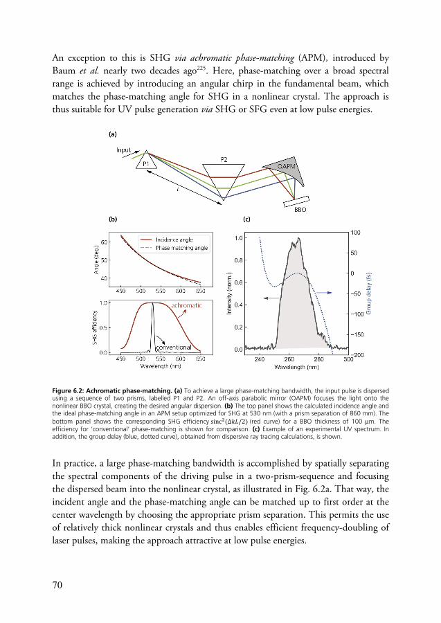
70
An exception to this is SHG via achromatic phase-matching (APM), introduced by Baum et al. nearly two decades ago225. Here, phase-matching over a broad spectral range is achieved by introducing an angular chirp in the fundamental beam, which matches the phase-matching angle for SHG in a nonlinear crystal. The approach is thus suitable for UV pulse generation via SHG or SFG even at low pulse energies.
Figure 6.2: Achromatic phase-matching. (a) To achieve a large phase-matching bandwidth, the input pulse is dispersed using a sequence of two prisms, labelled P1 and P2. An off-axis parabolic mirror (OAPM) focuses the light onto the nonlinear BBO crystal, creating the desired angular dispersion. (b) The top panel shows the calculated incidence angle and the ideal phase-matching angle in an APM setup optimized for SHG at 530 nm (with a prism separation of 860 mm). The bottom panel shows the corresponding SHG efficiency sinc (Δ𝑘𝐿/2) (red curve) for a BBO thickness of 100 μm. The efficiency for ‘conventional’ phase-matching is shown for comparison. (c) Example of an experimental UV spectrum. In addition, the group delay (blue, dotted curve), obtained from dispersive ray tracing calculations, is shown.
In practice, a large phase-matching bandwidth is accomplished by spatially separating the spectral components of the driving pulse in a two-prism-sequence and focusing the dispersed beam into the nonlinear crystal, as illustrated in Fig. 6.2a. That way, the incident angle and the phase-matching angle can be matched up to first order at the center wavelength by choosing the appropriate prism separation. This permits the use of relatively thick nonlinear crystals and thus enables efficient frequency-doubling of laser pulses, making the approach attractive at low pulse energies.
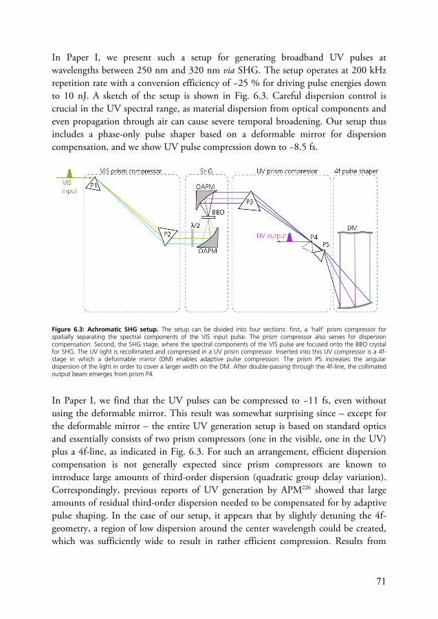
71
In Paper I, we present such a setup for generating broadband UV pulses at wavelengths between 250 nm and 320 nm via SHG. The setup operates at 200 kHz repetition rate with a conversion efficiency of ~25 % for driving pulse energies down to 10 nJ. A sketch of the setup is shown in Fig. 6.3. Careful dispersion control is crucial in the UV spectral range, as material dispersion from optical components and even propagation through air can cause severe temporal broadening. Our setup thus includes a phase-only pulse shaper based on a deformable mirror for dispersion compensation, and we show UV pulse compression down to ~8.5 fs.
Figure 6.3: Achromatic SHG setup. The setup can be divided into four sections: first, a ‘half’ prism compressor for spatially separating the spectral components of the VIS input pulse. The prism compressor also serves for dispersion compensation. Second, the SHG stage, where the spectral components of the VIS pulse are focused onto the BBO crystal for SHG. The UV light is recollimated and compressed in a UV prism compressor. Inserted into this UV compressor is a 4f-stage in which a deformable mirror (DM) enables adaptive pulse compression. The prism P5 increases the angular dispersion of the light in order to cover a larger width on the DM. After double-passing through the 4f-line, the collimated output beam emerges from prism P4.
In Paper I, we find that the UV pulses can be compressed to ~11 fs, even without using the deformable mirror. This result was somewhat surprising since – except for the deformable mirror – the entire UV generation setup is based on standard optics and essentially consists of two prism compressors (one in the visible, one in the UV) plus a 4f-line, as indicated in Fig. 6.3. For such an arrangement, efficient dispersion compensation is not generally expected since prism compressors are known to introduce large amounts of third-order dispersion (quadratic group delay variation). Correspondingly, previous reports of UV generation by APM226 showed that large amounts of residual third-order dispersion needed to be compensated for by adaptive pulse shaping. In the case of our setup, it appears that by slightly detuning the 4f-geometry, a region of low dispersion around the center wavelength could be created, which was sufficiently wide to result in rather efficient compression. Results from
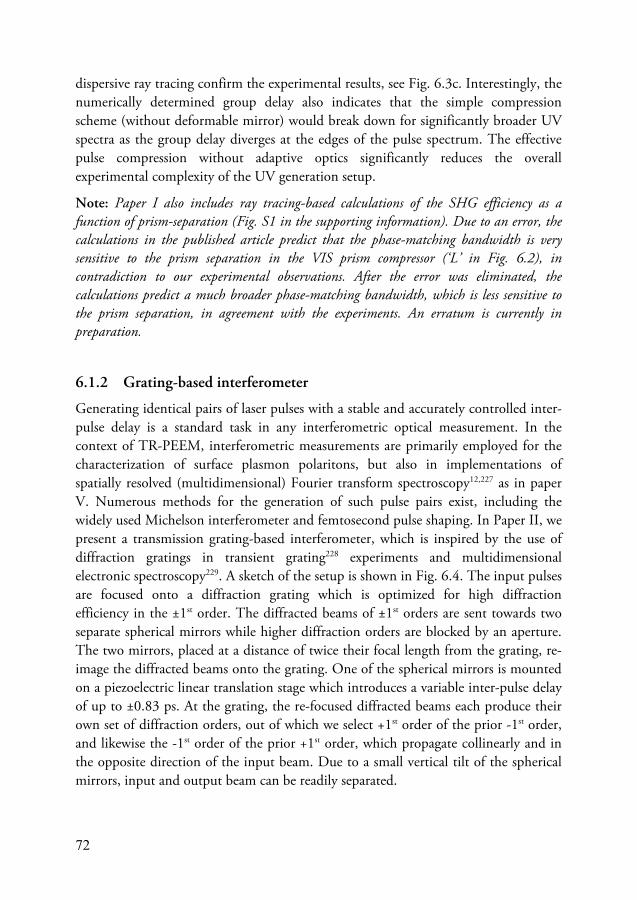
72
dispersive ray tracing confirm the experimental results, see Fig. 6.3c. Interestingly, the numerically determined group delay also indicates that the simple compression scheme (without deformable mirror) would break down for significantly broader UV spectra as the group delay diverges at the edges of the pulse spectrum. The effective pulse compression without adaptive optics significantly reduces the overall experimental complexity of the UV generation setup.
Note: Paper I also includes ray tracing-based calculations of the SHG efficiency as a function of prism-separation (Fig. S1 in the supporting information). Due to an error, the calculations in the published article predict that the phase-matching bandwidth is very sensitive to the prism separation in the VIS prism compressor (‘L’ in Fig. 6.2), in contradiction to our experimental observations. After the error was eliminated, the calculations predict a much broader phase-matching bandwidth, which is less sensitive to the prism separation, in agreement with the experiments. An erratum is currently in preparation.
6.1.2 Grating-based interferometer
Generating identical pairs of laser pulses with a stable and accurately controlled inter-pulse delay is a standard task in any interferometric optical measurement. In the context of TR-PEEM, interferometric measurements are primarily employed for the characterization of surface plasmon polaritons, but also in implementations of spatially resolved (multidimensional) Fourier transform spectroscopy12,227 as in paper V. Numerous methods for the generation of such pulse pairs exist, including thewidely used Michelson interferometer and femtosecond pulse shaping. In Paper II, wepresent a transmission grating-based interferometer, which is inspired by the use ofdiffraction gratings in transient grating228 experiments and multidimensionalelectronic spectroscopy229. A sketch of the setup is shown in Fig. 6.4. The input pulsesare focused onto a diffraction grating which is optimized for high diffractionefficiency in the ±1st order. The diffracted beams of ±1st orders are sent towards twoseparate spherical mirrors while higher diffraction orders are blocked by an aperture.The two mirrors, placed at a distance of twice their focal length from the grating, re-image the diffracted beams onto the grating. One of the spherical mirrors is mountedon a piezoelectric linear translation stage which introduces a variable inter-pulse delayof up to ±0.83 ps. At the grating, the re-focused diffracted beams each produce theirown set of diffraction orders, out of which we select +1st order of the prior -1st order,and likewise the -1st order of the prior +1st order, which propagate collinearly and inthe opposite direction of the input beam. Due to a small vertical tilt of the sphericalmirrors, input and output beam can be readily separated.
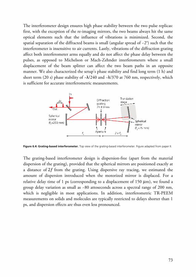
73
The interferometer design ensures high phase stability between the two pulse replicas: first, with the exception of the re-imaging mirrors, the two beams always hit the same optical elements such that the influence of vibrations is minimized. Second, the spatial separation of the diffracted beams is small (angular spread of ~2°) such that the interferometer is insensitive to air currents. Lastly, vibrations of the diffraction grating affect both interferometer arms equally and do not affect the phase delay between the pulses, as opposed to Michelson or Mach-Zehnder interferometers where a small displacement of the beam splitter can affect the two beam paths in an opposite manner. We also characterized the setup’s phase stability and find long term (1 h) and short term (20 s) phase stability of ~λ/240 and ~λ/370 at 760 nm, respectively, which is sufficient for accurate interferometric measurements.
Figure 6.4: Grating-based interferometer. Top view of the grating-based interferometer. Figure adapted from paper II.
The grating-based interferometer design is dispersion-free (apart from the material dispersion of the grating), provided that the spherical mirrors are positioned exactly at a distance of 2𝑓 from the grating. Using dispersive ray tracing, we estimated the amount of dispersion introduced when the motorized mirror is displaced. For a relative delay time of 1 ps (corresponding to a displacement of 150 μm), we found a group delay variation as small as ~80 attoseconds across a spectral range of 200 nm, which is negligible in most applications. In addition, interferometric TR-PEEM measurements on solids and molecules are typically restricted to delays shorter than 1 ps, and dispersion effects are thus even less pronounced.
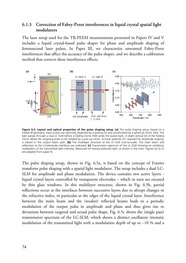
74
6.1.3 Correction of Fabry-Perot interferences in liquid crystal spatial light modulators
The laser setup used for the TR-PEEM measurements presented in Papers IV and V includes a liquid crystal-based pulse shaper for phase and amplitude shaping of femtosecond laser pulses. In Paper III, we characterize unwanted Fabry-Perot interferences that affect the accuracy of the pulse shaper, and we describe a calibration method that corrects these interference effects.
Figure 6.5: Layout and optical properties of the pulse shaping setup. (a) The pulse shaping setup, based on a folded 4f-geometry. Input pulses are spectrally dispersed by a grating (G) and recollimated by a spherical mirror (SM). The light passes through a dual LC-SLM before a folding mirror (FM) sends the pulses back. A slight vertical tilt of the folding mirror allows the outgoing pulse to be isolated by a pick-up mirror. A linear polarizer (P), required for amplitude shaping, is placed in the output beam path. (b) The multilayer structure of the LC-SLM (not-to-scale). The main beam and reflections at the LC/electrode interfaces are indicated. (c) Transmission spectrum of the LC-SLM showing an oscillatory modulation of the transmitted light intensity. Measured for linearly polarized light, as shown in the inset. Figures (a) to (c) are adapted from paper III.
The pulse shaping setup, shown in Fig. 6.5a, is based on the concept of Fourier transform pulse shaping with a spatial light modulator. The setup includes a dual LC-SLM for amplitude and phase modulation. The device contains two active layers - liquid crystal layers controlled by transparent electrodes – which in turn are encased by thin glass windows. In this multilayer structure, shown in Fig. 6.5b, partial reflections occur at the interfaces between successive layers due to abrupt changes in the refractive index, in particular at the edges of the liquid crystal layer. Interference between the main beam and the (weaker) reflected beams leads to a periodic modulation of the output pulse in amplitude and phase and thus gives rise to deviations between targeted and actual pulse shape. Fig. 6.5c shows the (single pass) transmission spectrum of the LC-SLM, which shows a distinct oscillatory intensity modulation of the transmitted light with a modulation depth of up to ~10 % and a
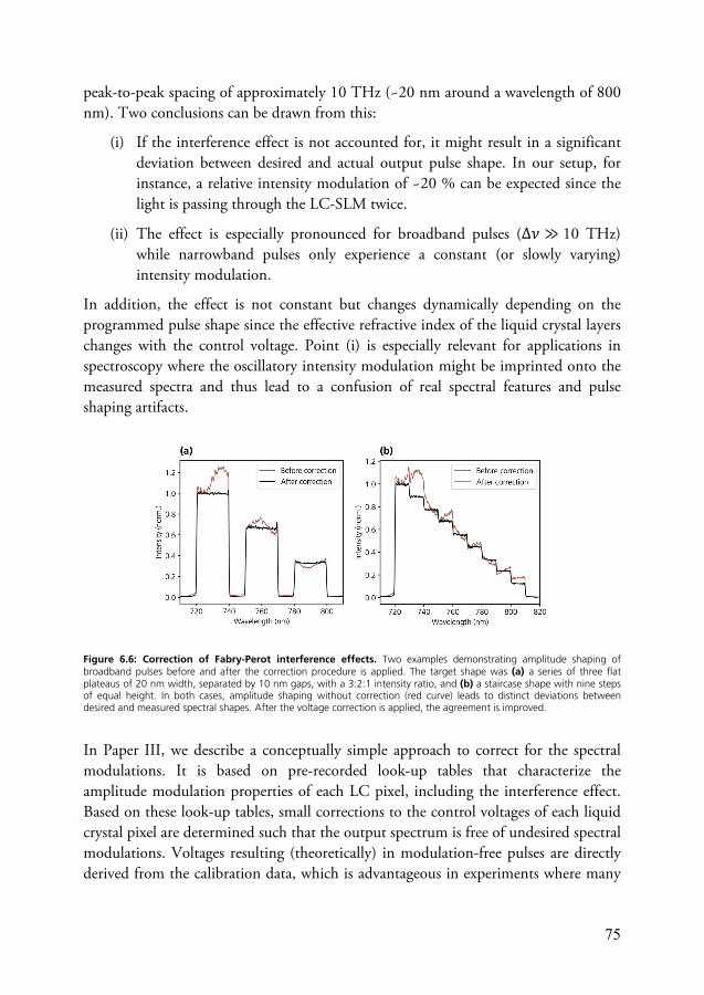
75
peak-to-peak spacing of approximately 10 THz (~20 nm around a wavelength of 800 nm). Two conclusions can be drawn from this:
(i) If the interference effect is not accounted for, it might result in a significant deviation between desired and actual output pulse shape. In our setup, for instance, a relative intensity modulation of ~20 % can be expected since the light is passing through the LC-SLM twice.
(ii) The effect is especially pronounced for broadband pulses (Δ𝜈 ≫ 10 THz) while narrowband pulses only experience a constant (or slowly varying) intensity modulation.
In addition, the effect is not constant but changes dynamically depending on the programmed pulse shape since the effective refractive index of the liquid crystal layers changes with the control voltage. Point (i) is especially relevant for applications in spectroscopy where the oscillatory intensity modulation might be imprinted onto the measured spectra and thus lead to a confusion of real spectral features and pulse shaping artifacts.
Figure 6.6: Correction of Fabry-Perot interference effects. Two examples demonstrating amplitude shaping of broadband pulses before and after the correction procedure is applied. The target shape was (a) a series of three flat plateaus of 20 nm width, separated by 10 nm gaps, with a 3:2:1 intensity ratio, and (b) a staircase shape with nine steps of equal height. In both cases, amplitude shaping without correction (red curve) leads to distinct deviations between desired and measured spectral shapes. After the voltage correction is applied, the agreement is improved.
In Paper III, we describe a conceptually simple approach to correct for the spectral modulations. It is based on pre-recorded look-up tables that characterize the amplitude modulation properties of each LC pixel, including the interference effect. Based on these look-up tables, small corrections to the control voltages of each liquid crystal pixel are determined such that the output spectrum is free of undesired spectral modulations. Voltages resulting (theoretically) in modulation-free pulses are directly derived from the calibration data, which is advantageous in experiments where many
76
different pulse shapes need to be generated. Some examples of shaped pulses before and after the voltage correction has been applied are shown in Fig. 6.6, demonstrating efficient suppression of the spectral modulations.
While the interference effect leads to a spectral modulation in both amplitude and phase, the correction procedure implemented in Paper III is specifically designed to correct for the amplitude modulation of the spectrum (This has practical reasons. The amplitude modulation introduced by each pixel can be readily measured, while a direct characterization of the phase delay is far more complicated). When the experiments of Paper III were carried out, a pulse characterization method for retrieval of the full electric field of the pulse was not yet implemented in the setup. An interesting follow-up experiment would thus be the complete characterization of shaped pulses before and after the correction is applied to investigate whether the phase modulation is also corrected for. Characterization of shaped pulses carried out thus far was based on intensity autocorrelation measurements, which only reveal information about the general pulse shape but do not provide the spectral phase. Still, no indications of oscillatory spectral phase modulations, such as satellite pulses in the time domain, could be observed.
6.2 PEEM applications
6.2.1 Hot electron relaxation in InAs nanowires
The properties and relaxation dynamics of photogenerated hot carriers in nanostructures have been intensely investigated based on the incentive that harnessing the excess thermal energy of these carriers could enable new and efficient ways to detect light230 or catalyze chemical reactions at surfaces169. Another potential application is the hot carrier solar cell: if photoexcited carriers can be extracted before their excess thermal energy is dissipated, solar cells with conversion efficiencies beyond the Shockley-Queisser limit231 are theoretically possible. While the extraction of a hot-carrier photocurrent has been demonstrated experimentally160,232,233, the construction of a hot-carrier solar cell with significant conversion efficiency has hitherto not been realized.
III-V semiconductor nanowires are an attractive platform for exploring design pattensfor hot carrier solar cells, as complex engineering of band profiles is possible innanowire heterostructures94,233. In Paper IV, we use TR-PEEM to investigate the
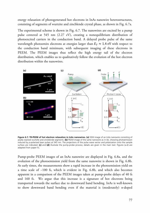
77
energy relaxation of photogenerated hot electrons in InAs nanowire heterostructures, consisting of segments of wurtzite and zincblende crystal phase, as shown in Fig. 6.7a.
The experimental scheme is shown in Fig. 6.7. The nanowires are excited by a pump pulse centered at 545 nm (2.27 eV), creating a nonequilibrium distribution of photoexcited carriers in the conduction band. A delayed probe pulse of the same wavelength photoemits electrons at energies larger than 𝐸 ≈ 1.4 eV with respect to the conduction band minimum, with subsequent imaging of these electrons in PEEM. The PEEM images thus reflect the high energy tail of the electron distribution, which enables us to qualitatively follow the evolution of the hot electron distribution within the nanowires.
Figure 6.7: TR-PEEM of hot electron relaxation in InAs nanowires. (a) SEM image of an InAs nanowire consisting of axially stacked wurtzite and zincblende segments. (b) PEEM image of the same nanowire as in (b), showing photoemission induced by p-polarized laser pulses at 545 nm. The projections of the pulse wave vector and polarization onto the sample surface are indicated. (c) and (d) illustrate the pump-probe process; details are given in the main text. Figures (a-d) are adapted from paper IV.
Pump-probe PEEM images of an InAs nanowire are displayed in Fig. 6.8a, and the evolution of the photoemission yield from the same nanowire is shown in Fig. 6.8b. At early times, the measurements show a rapid increase in the photoemission yield on a time scale of ~100 fs, which is evident in Fig. 6.8b, and which also becomes apparent in a comparison of the PEEM images taken at pump-probe delays of 40 fs and 160 fs. We argue that this increase is a signature of hot electrons being transported towards the surface due to downward band bending. InAs is well-known to show downward band bending even if the material is (moderately) n-doped
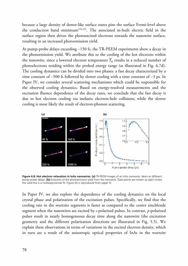
78
because a large density of donor-like surface states pins the surface Fermi-level above the conduction band minimum234,235. The associated in-built electric field in the surface region then drives the photoexcited electrons towards the nanowire surface, resulting in an increased photoemission yield.
At pump-probe delays exceeding ~150 fs, the TR-PEEM experiments show a decay in the photoemission yield. We attribute this to the cooling of the hot electrons within the nanowire, since a lowered electron temperature 𝑇 results in a reduced number of photoelectrons residing within the probed energy range (as illustrated in Fig. 6.7d). The cooling dynamics can be divided into two phases: a fast decay characterized by a time constant of ~500 fs followed by slower cooling with a time constant of ~3 ps. In Paper IV, we consider several scattering mechanisms which could be responsible for the observed cooling dynamics. Based on energy-resolved measurements and the excitation fluence dependence of the decay rates, we conclude that the fast decay is due to hot electron cooling via inelastic electron-hole collisions, while the slower cooling is most likely the result of electron-phonon scattering.
Figure 6.8: Hot electron relaxation in InAs nanowires. (a) TR-PEEM images of an InAs nanowire, taken at different pump-probe delays. (b) Evolution of the photoemission yield from the nanowire. Data points are shown as open circles; the solid line is a multiexponential fit. Figure (b) is reproduced from paper IV.
In Paper IV, we also explore the dependence of the cooling dynamics on the local crystal phase and polarization of the excitation pulses. Specifically, we find that the cooling rate in the wurtzite segments is faster as compared to the center zincblende segment when the nanowires are excited by s-polarized pulses. In contrast, p-polarized pulses result in nearly homogeneous decay time along the nanowire (the excitation geometry and the different polarization directions are illustrated in Fig. 5.5). We explain these observations in terms of variations in the excited electron density, which in turn are a result of the anisotropic optical properties of InAs in the wurtzite
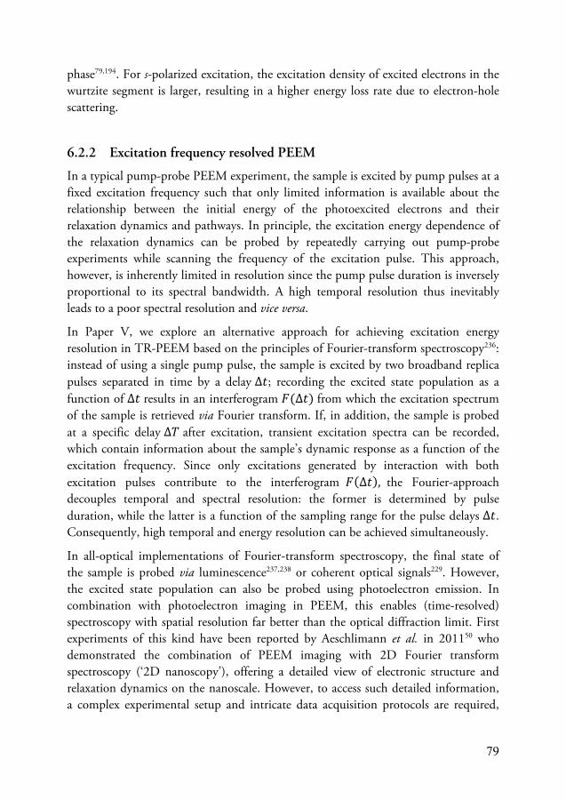
79
phase79,194. For s-polarized excitation, the excitation density of excited electrons in the wurtzite segment is larger, resulting in a higher energy loss rate due to electron-hole scattering.
6.2.2 Excitation frequency resolved PEEM
In a typical pump-probe PEEM experiment, the sample is excited by pump pulses at a fixed excitation frequency such that only limited information is available about the relationship between the initial energy of the photoexcited electrons and their relaxation dynamics and pathways. In principle, the excitation energy dependence of the relaxation dynamics can be probed by repeatedly carrying out pump-probe experiments while scanning the frequency of the excitation pulse. This approach, however, is inherently limited in resolution since the pump pulse duration is inversely proportional to its spectral bandwidth. A high temporal resolution thus inevitably leads to a poor spectral resolution and vice versa.
In Paper V, we explore an alternative approach for achieving excitation energy resolution in TR-PEEM based on the principles of Fourier-transform spectroscopy236: instead of using a single pump pulse, the sample is excited by two broadband replica pulses separated in time by a delay Δ𝑡; recording the excited state population as a function of Δ𝑡 results in an interferogram 𝐹(Δ𝑡) from which the excitation spectrum of the sample is retrieved via Fourier transform. If, in addition, the sample is probed at a specific delay Δ𝑇 after excitation, transient excitation spectra can be recorded, which contain information about the sample’s dynamic response as a function of the excitation frequency. Since only excitations generated by interaction with both excitation pulses contribute to the interferogram 𝐹(Δ𝑡), the Fourier-approach decouples temporal and spectral resolution: the former is determined by pulse duration, while the latter is a function of the sampling range for the pulse delays Δ𝑡. Consequently, high temporal and energy resolution can be achieved simultaneously.
In all-optical implementations of Fourier-transform spectroscopy, the final state of the sample is probed via luminescence237,238 or coherent optical signals229. However, the excited state population can also be probed using photoelectron emission. In combination with photoelectron imaging in PEEM, this enables (time-resolved) spectroscopy with spatial resolution far better than the optical diffraction limit. First experiments of this kind have been reported by Aeschlimann et al. in 201150 who demonstrated the combination of PEEM imaging with 2D Fourier transform spectroscopy (‘2D nanoscopy’), offering a detailed view of electronic structure and relaxation dynamics on the nanoscale. However, to access such detailed information, a complex experimental setup and intricate data acquisition protocols are required,
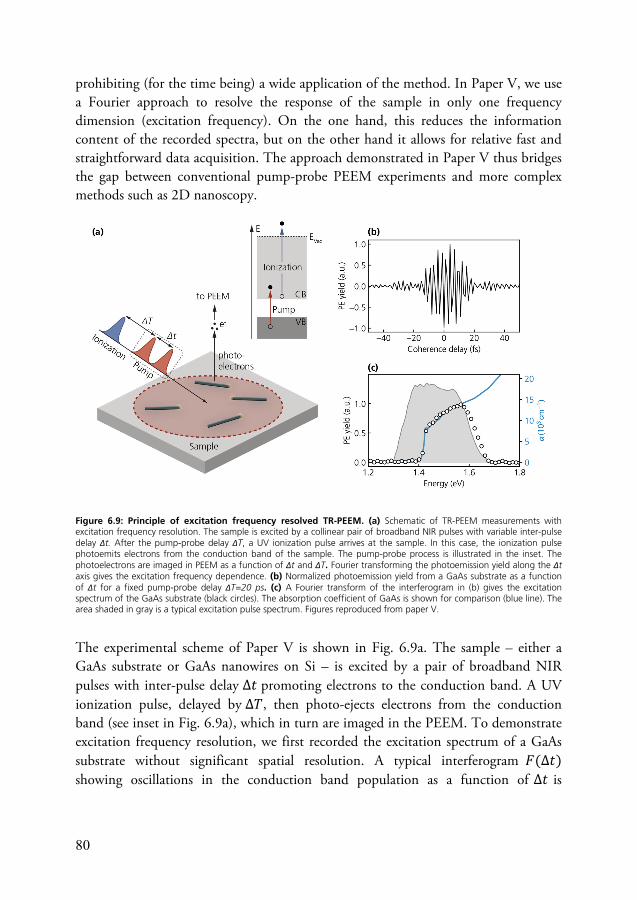
80
prohibiting (for the time being) a wide application of the method. In Paper V, we use a Fourier approach to resolve the response of the sample in only one frequency dimension (excitation frequency). On the one hand, this reduces the information content of the recorded spectra, but on the other hand it allows for relative fast and straightforward data acquisition. The approach demonstrated in Paper V thus bridges the gap between conventional pump-probe PEEM experiments and more complex methods such as 2D nanoscopy.
Figure 6.9: Principle of excitation frequency resolved TR-PEEM. (a) Schematic of TR-PEEM measurements with excitation frequency resolution. The sample is excited by a collinear pair of broadband NIR pulses with variable inter-pulse delay Δt. After the pump-probe delay ΔT, a UV ionization pulse arrives at the sample. In this case, the ionization pulse photoemits electrons from the conduction band of the sample. The pump-probe process is illustrated in the inset. The photoelectrons are imaged in PEEM as a function of Δt and ΔT. Fourier transforming the photoemission yield along the Δt axis gives the excitation frequency dependence. (b) Normalized photoemission yield from a GaAs substrate as a function of Δt for a fixed pump-probe delay ΔT=20 ps. (c) A Fourier transform of the interferogram in (b) gives the excitation spectrum of the GaAs substrate (black circles). The absorption coefficient of GaAs is shown for comparison (blue line). The area shaded in gray is a typical excitation pulse spectrum. Figures reproduced from paper V.
The experimental scheme of Paper V is shown in Fig. 6.9a. The sample – either a GaAs substrate or GaAs nanowires on Si – is excited by a pair of broadband NIR pulses with inter-pulse delay Δ𝑡 promoting electrons to the conduction band. A UV ionization pulse, delayed by Δ𝑇, then photo-ejects electrons from the conduction band (see inset in Fig. 6.9a), which in turn are imaged in the PEEM. To demonstrate excitation frequency resolution, we first recorded the excitation spectrum of a GaAs substrate without significant spatial resolution. A typical interferogram 𝐹(Δ𝑡) showing oscillations in the conduction band population as a function of Δ𝑡 is
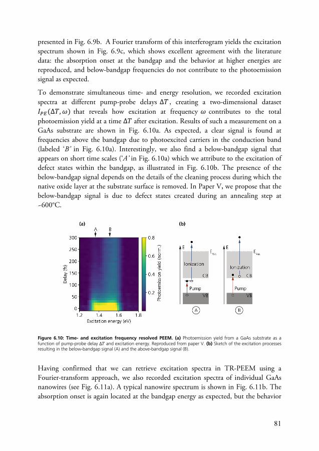
81
presented in Fig. 6.9b. A Fourier transform of this interferogram yields the excitation spectrum shown in Fig. 6.9c, which shows excellent agreement with the literature data: the absorption onset at the bandgap and the behavior at higher energies are reproduced, and below-bandgap frequencies do not contribute to the photoemission signal as expected.
To demonstrate simultaneous time- and energy resolution, we recorded excitation spectra at different pump-probe delays Δ𝑇 , creating a two-dimensional dataset 𝐼 (Δ𝑇, 𝜔) that reveals how excitation at frequency 𝜔 contributes to the total photoemission yield at a time Δ𝑇 after excitation. Results of such a measurement on a GaAs substrate are shown in Fig. 6.10a. As expected, a clear signal is found at frequencies above the bandgap due to photoexcited carriers in the conduction band (labeled ‘B’ in Fig. 6.10a). Interestingly, we also find a below-bandgap signal that appears on short time scales (‘A’ in Fig. 6.10a) which we attribute to the excitation of defect states within the bandgap, as illustrated in Fig. 6.10b. The presence of the below-bandgap signal depends on the details of the cleaning process during which the native oxide layer at the substrate surface is removed. In Paper V, we propose that the below-bandgap signal is due to defect states created during an annealing step at ~600°C.
Figure 6.10: Time- and excitation frequency resolved PEEM. (a) Photoemission yield from a GaAs substrate as a function of pump-probe delay Δ𝑇 and excitation energy. Reproduced from paper V. (b) Sketch of the excitation processes resulting in the below-bandgap signal (A) and the above-bandgap signal (B).
Having confirmed that we can retrieve excitation spectra in TR-PEEM using a Fourier-transform approach, we also recorded excitation spectra of individual GaAs nanowires (see Fig. 6.11a). A typical nanowire spectrum is shown in Fig. 6.11b. The absorption onset is again located at the bandgap energy as expected, but the behavior
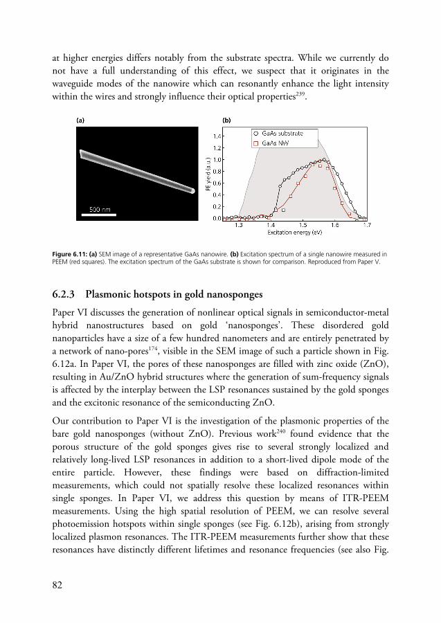
82
at higher energies differs notably from the substrate spectra. While we currently do not have a full understanding of this effect, we suspect that it originates in the waveguide modes of the nanowire which can resonantly enhance the light intensity within the wires and strongly influence their optical properties239.
Figure 6.11: (a) SEM image of a representative GaAs nanowire. (b) Excitation spectrum of a single nanowire measured in PEEM (red squares). The excitation spectrum of the GaAs substrate is shown for comparison. Reproduced from Paper V.
6.2.3 Plasmonic hotspots in gold nanosponges
Paper VI discusses the generation of nonlinear optical signals in semiconductor-metal hybrid nanostructures based on gold ‘nanosponges’. These disordered gold nanoparticles have a size of a few hundred nanometers and are entirely penetrated by a network of nano-pores174, visible in the SEM image of such a particle shown in Fig. 6.12a. In Paper VI, the pores of these nanosponges are filled with zinc oxide (ZnO), resulting in Au/ZnO hybrid structures where the generation of sum-frequency signals is affected by the interplay between the LSP resonances sustained by the gold sponges and the excitonic resonance of the semiconducting ZnO.
Our contribution to Paper VI is the investigation of the plasmonic properties of the bare gold nanosponges (without ZnO). Previous work240 found evidence that the porous structure of the gold sponges gives rise to several strongly localized and relatively long-lived LSP resonances in addition to a short-lived dipole mode of the entire particle. However, these findings were based on diffraction-limited measurements, which could not spatially resolve these localized resonances within single sponges. In Paper VI, we address this question by means of ITR-PEEM measurements. Using the high spatial resolution of PEEM, we can resolve several photoemission hotspots within single sponges (see Fig. 6.12b), arising from strongly localized plasmon resonances. The ITR-PEEM measurements further show that these resonances have distinctly different lifetimes and resonance frequencies (see also Fig.
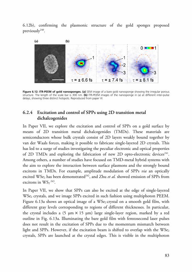
83
6.12b), confirming the plasmonic structure of the gold sponges proposed previously240.
Figure 6.12: ITR-PEEM of gold nanosponges. (a) SEM image of a bare gold nanosponge showing the irregular porous structure. The length of the scale bar is 300 nm. (b) ITR-PEEM images of the nanosponge in (a) at different inter-pulse delays, showing three distinct hotspots. Reproduced from paper VI.
6.2.4 Excitation and control of SPPs using 2D transition metal dichalcogenides
In Paper VII, we explore the excitation and control of SPPs on a gold surface by means of 2D transition metal dichalcogenides (TMDs). These materials are semiconductors whose bulk crystals consist of 2D layers weakly bound together by van der Waals forces, making it possible to fabricate single-layered 2D crystals. This has led to a surge of studies investigating the peculiar electronic and optical properties of 2D TMDs and exploring the fabrication of new 2D opto-electronic devices241. Among others, a number of studies have focused on TMD-metal hybrid systems with the aim to explore the interaction between surface plasmons and the strongly bound excitons in TMDs. For example, amplitude modulation of SPPs via an optically excited WSe2 has been demonstrated242, and Zhu et al. showed emission of SPPs from excitons in WS2
243.
In Paper VII, we show that SPPs can also be excited at the edge of single-layered WSe2 crystals, and we image SPPs excited in such fashion using multiphoton PEEM. Figure 6.13a shows an optical image of a WSe2 crystal on a smooth gold film, with different gray levels corresponding to regions of different thicknesses. In particular, the crystal includes a (5 μm × 15 μm) large single-layer region, marked by a red outline in Fig. 6.13a. Illuminating the bare gold film with femtosecond laser pulses does not result in the excitation of SPPs due to the momentum mismatch between light and SPPs. However, if the excitation beam is shifted to overlap with the WSe2 crystals, SPPs are launched at the crystal edges. This is visible in the multiphoton
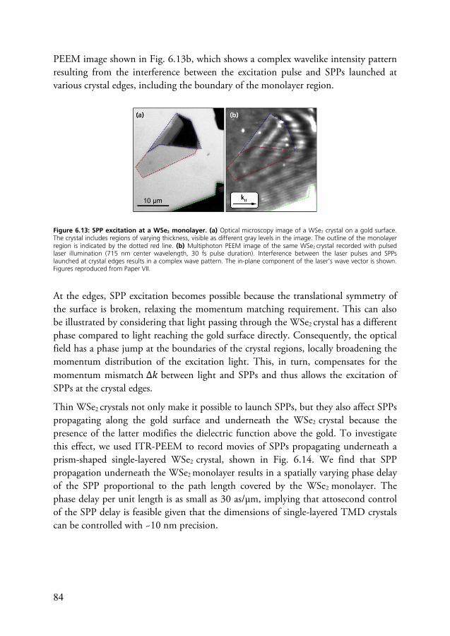
84
PEEM image shown in Fig. 6.13b, which shows a complex wavelike intensity pattern resulting from the interference between the excitation pulse and SPPs launched at various crystal edges, including the boundary of the monolayer region.
Figure 6.13: SPP excitation at a WSe2 monolayer. (a) Optical microscopy image of a WSe2 crystal on a gold surface. The crystal includes regions of varying thickness, visible as different gray levels in the image. The outline of the monolayer region is indicated by the dotted red line. (b) Multiphoton PEEM image of the same WSe2 crystal recorded with pulsed laser illumination (715 nm center wavelength, 30 fs pulse duration). Interference between the laser pulses and SPPs launched at crystal edges results in a complex wave pattern. The in-plane component of the laser’s wave vector is shown. Figures reproduced from Paper VII.
At the edges, SPP excitation becomes possible because the translational symmetry of the surface is broken, relaxing the momentum matching requirement. This can also be illustrated by considering that light passing through the WSe2 crystal has a different phase compared to light reaching the gold surface directly. Consequently, the optical field has a phase jump at the boundaries of the crystal regions, locally broadening the momentum distribution of the excitation light. This, in turn, compensates for the momentum mismatch Δ𝑘 between light and SPPs and thus allows the excitation of SPPs at the crystal edges.
Thin WSe2 crystals not only make it possible to launch SPPs, but they also affect SPPs propagating along the gold surface and underneath the WSe2 crystal because the presence of the latter modifies the dielectric function above the gold. To investigate this effect, we used ITR-PEEM to record movies of SPPs propagating underneath a prism-shaped single-layered WSe2 crystal, shown in Fig. 6.14. We find that SPP propagation underneath the WSe2 monolayer results in a spatially varying phase delay of the SPP proportional to the path length covered by the WSe2 monolayer. The phase delay per unit length is as small as 30 as/μm, implying that attosecond control of the SPP delay is feasible given that the dimensions of single-layered TMD crystals can be controlled with ~10 nm precision.
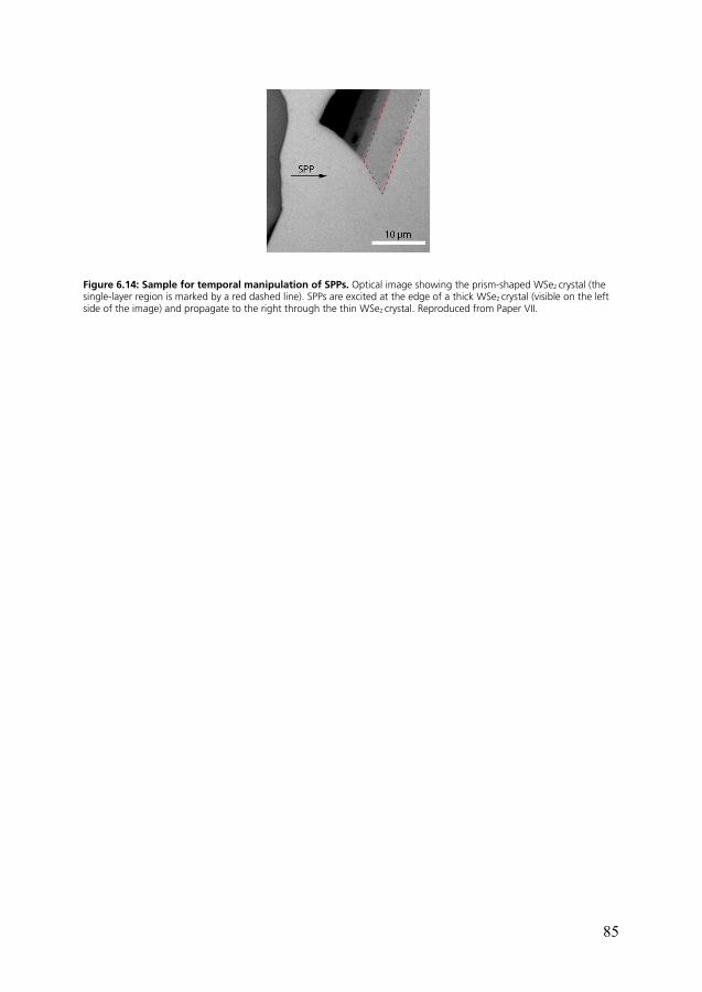
85
Figure 6.14: Sample for temporal manipulation of SPPs. Optical image showing the prism-shaped WSe2 crystal (the single-layer region is marked by a red dashed line). SPPs are excited at the edge of a thick WSe2 crystal (visible on the left side of the image) and propagate to the right through the thin WSe2 crystal. Reproduced from Paper VII.

87
7 Concluding Remarks and Outlook
This thesis describes our contributions to the field of ultrafast time-resolved photoemission electron microscopy, which fall into either of two categories: first, developments in ultrafast optics for the generation and control of femtosecond laser pulses with the aim to advance TR-PEEM experiments. And second, applications of TR-PEEM in studies of ultrafast photoexcitation dynamics in metal and semiconductor nanostructures.
As femtosecond laser pulses are an integral ingredient in any ultrafast time-resolved PEEM measurement, the range of possible experiments critically depends on the availability of advanced laser sources and the ability to accurately control ultrashort optical pulses. Parameters of particular importance in TR-PEEM are laser stability (due to the comparatively slow imaging process) and the pulse repetition rate (due to space charge effects). The latter point was addressed in Paper I where we demonstrated efficient generation of broadband UV pulses around ~4.7 eV with ~10 fs pulse duration at repetition rates of 200 kHz. Laser sources in this photon energy range are required to overcome the work function of many relevant solids, and they thus allow the investigation of charge carrier dynamics at energies down to the Fermi level in photoemission experiments. In future TR-PEEM studies, these results will be used to obtain a comprehensive picture of electron intra- and inter-band relaxation on time scales down to few tens of femtoseconds. A first application of the UV source in TR-PEEM experiments led to the results described in Paper V.
The improvement of the optical setup also included the development of a stable yet simple interferometer design and the characterization and compensation of unwanted interference effects in a liquid crystal-based pulse shaper. The pulse shaper has so far not been included in the TR-PEEM experiments. However, there are certainly many interesting possibilities for using it in the future, from flexible pulse compression to the generation of pulse sequences for time-domain spectroscopy or adaptive pulse shaping for coherent control of excitations in nanostructures. Finally, while the work presented in Papers I to III was carried out with the goal to enable new kinds of TR-PEEM experiments in our laboratory, the results can also be applied in many other
88
contexts and should be of value to the broader ultrafast optics and spectroscopy community.
TR-PEEM is today firmly established in plasmonics research as a tool for ultrafast imaging of optical near-fields at surfaces. Following the first studies carried out in the early 2000s, the technique has advanced dramatically, and correspondingly, TR-PEEM experiments on plasmonic systems have become increasingly sophisticated, as witnessed by demonstrations of spatiotemporal control of plasmonic excitations49, energy transfer between localized modes244 or full reconstruction of SPP fields214. In addition, several studies have resolved the local near-field within single plasmonic nanoparticles19,168,245. Such a study is also presented in Paper VI where we investigate porous gold nano-particles and can directly show that the disordered structure of these particles sustains several strongly localized plasmonic hotspots of varying frequencies and dephasing times. TR-PEEM studies of LSP resonances in noble metal nanoparticles, including Paper VI, commonly focus on the properties of the plasmonic near-field. An interesting extension of such studies would be (time-resolved) imaging of hot electrons which are generated as a product of plasmon decay. Evidence for correlation between the spatial characteristics of the plasmonic near-field and the local hot-carrier generation rate has been found previously246, and spatially- and time-resolved studies of hot-carrier relaxation within single plasmonic nano-particles would certainly be very intriguing.
In Paper VII we demonstrate excitation and control of SPPs on gold using single-layer WSe2 crystals. On the one hand, the efficiency of this SPP excitation mechanism is well below that of conventional SPP excitation approaches using grooves or holes cut into the metal surface. On the other hand, such grooves are at least tens of nanometers deep while the height of a WSe2 monolayer is below 1 nm, and SPP excitation at the edge of a WSe2 monolayer might thus be attractive if compactness is favored over efficiency. We also find that SPPs propagating underneath a WSe2
monolayer experience a phase delay that can, in principle, be controlled on the attosecond level with current fabrication technologies247. This raises the question of whether the SPP phase delay may also be dynamically adjusted by optical or electrical gating.
Another development within the field of TR-PEEM is the investigation of photoexcited charge carriers at semiconductor surfaces. After the first proof-of-concept experiments in 2014206, the number of TR-PEEM studies in this area has steadily increased, addressing processes such as electron transport248, hot carrier relaxation205 or carrier trapping11. Our contributions to this field are presented in Papers IV and V. In the former, we follow the intra-band relaxation of photogenerated ‘hot’ electrons in InAs nanowires and identify mechanisms relevant
89
for energy dissipation and hot electron transport on a sub-picosecond time scale. In this study we use a one-color pump-probe approach with visible pulses, which offers the benefits of a simple experimental setup, a high signal-to-background ratio and which allows us to follow hot electron cooling without the need to spectrally resolve the photoelectrons. On the downside, this approach does not provide access the full electron energy distribution, and the fastest dynamics are hidden by pulse overlap effects. In the future, Paper IV could thus be complemented by two-color experiments exploring the evolution of the electron distribution at the very early stages of the relaxation cascade.
In Paper V, we combined two-color pump-probe PEEM with a time-domain spectroscopy approach, allowing us to resolve electron relaxation dynamics with respect to the optical excitation frequency. We could demonstrate the feasibility of the approach using GaAs substrates as a benchmark system. Excitation frequency resolution should be especially valuable in contexts where the initial energy of photoexcited electrons decisively affects their relaxation pathway, for instance, at Schottky barriers or in nanowire heterostructures with energy barriers. In Papers IV and V, we could observe vertical electron transport, which sensitively depended on the surface condition, underlining the importance of having good control over the surface in TR-PEEM studies of (III-V) semiconductors.
There are many possible paths ahead for the exploration of ultrafast dynamics on the nanoscale with TR-PEEM, some of which have been sketched above. One such direction is the further integration of time-domain spectroscopy methods into TR-PEEM. First experiments of this kind combined PEEM with 2D spectroscopy50. However, the number of such studies has been limited so far, in large parts due to their experimental complexity and long acquisition times. This might change when amplified laser systems operating at MHz repetition rates become more widely available199. In the meantime, simplified approaches such as the one discussed in Paper V may also provide interesting insights while being technologically less demanding.
A long-standing goal within nano-optics research is the direct determination of optical near-fields with sub-cycle temporal resolution. This motivated a theoretical proposal in 2007249 which suggested combining PEEM with attosecond XUV pulses to achieve attosecond-resolution imaging of plasmonic fields (‘atto-PEEM’). From a technological standpoint, this combination is immensely challenging. Still, important steps towards its realization have been taken204,221, including the development of a high repetition rate source of attosecond XUV pulses at Lund University65. This is indispensable for high resolution PEEM imaging, bringing atto-PEEM closer to

90
experimental realization and possibly leading to other pump-probe PEEM experiments based on core-level photoemission.
Finally, as TR-PEEM on semiconductor systems becomes more established, I expect an increased number of studies where TR-PEEM is used in concert with other techniques in more application-oriented research, as in previous studies on light absorption12 and carrier trapping11 in solar cell materials.
91
References
(1) Arbouet, A.; Caruso, G. M.; Houdellier, F. Ultrafast Transmission Electron Microscopy: Historical Development, Instrumentation, and Applications; Elsevier Inc., 2018; Vol. 207.
(2) Gross, L.; Mohn, F.; Moll, N.; Liljeroth, P.; Meyer, G. The Chemical Structure of a Molecule Resolved by Atomic Force Microscopy. Science 2009, 325 (5944), 1110–1114.
(3) Science of Microscopy; Hawkes, P. W., Spence, J. C. H., Eds.; Springer New York: New York, NY, 2007.
(4) Maiman; T. H. Stimulated Optical Radiation in Ruby. Nature 1960, 187 (4736), 493–494.
(5) Dostál, J.; Pšenčík, J.; Zigmantas, D. In Situ Mapping of the Energy Flow through the Entire Photosynthetic Apparatus. Nat. Chem. 2016, 8 (7), 705–710.
(6) Shah, J. Ultrafast Spectroscopy of Semiconductors and Semiconductor Nanostructures; Springer Berlin Heidelberg: Berlin, 1999.
(7) Ippen, E. P. Principles of Passive Mode Locking. Appl. Phys. B Laser Opt. 1994, 58 (3), 159–170.
(8) Zewail, A. H. Four-Dimensional Electron Microscopy. 2010, 328 (April), 187–194.
(9) Vogelsang, J.; Hergert, G.; Wang, D.; Groß, P.; Lienau, C. Observing Charge Separation in Nanoantennas via Ultrafast Point-Projection Electron Microscopy. Light Sci. Appl. 2018, 7 (1), 4–11.
(10) Lloyd-Hughes, J.; Oppeneer, P. M.; Pereira dos Santos, T.; Schleife, A.; Meng, S.; Sentef, M. A.; Ruggenthaler, M.; Rubio, A.; Radu, I.; Murnane, M.; Shi, X.; Kapteyn, H.; Stadtmüller, B.; Dani, K. M.; da Jornada, F. H.; Prinz, E.; Aeschlimann, M.; Milot, R. L.; Burdanova, M.; Boland, J.; Cocker, T.; Hegmann, F. The 2021 Ultrafast Spectroscopic Probes of Condensed Matter Roadmap. J. Phys. Condens. Matter 2021, 33 (35), 353001.
(11) Doherty, T. A. S.; Winchester, A. J.; Macpherson, S.; Johnstone, D. N.; Pareek, V.; Tennyson, E. M.; Kosar, S.; Kosasih, F. U.; Anaya, M.; Abdi-Jalebi, M.; Andaji-Garmaroudi, Z.; Wong, E. L.; Madéo, J.; Chiang, Y.; Park, J.; Jung, Y.; Petoukhoff, C. E.; Divitini, G.; Man, M. K. L.; Ducati, C.; Walsh, A.; Midgley, P. A.; Dani, K. M.; Stranks, S. D. Performance-Limiting Nanoscale Trap Clusters at Grain Junctions in Halide Perovskites. Nature 2020, 580 (7803), 360–366.
(12) Aeschlimann, M.; Brixner, T.; Differt, D.; Heinzmann, U.; Hensen, M.; Kramer, C.; Lükermann, F.; Melchior, P.; Pfeiffer, W.; Piecuch, M.; Schneider, C.; Stiebig, H.; Strüber, C.; Thielen, P. Perfect Absorption in Nanotextured Thin Films via Anderson-Localized Photon Modes. Nat. Photonics 2015, 9 (10), 663–668.
(13) Brongersma, M. L.; Halas, N. J.; Nordlander, P. Plasmon-Induced Hot Carrier Science and Technology. Nat. Nanotechnol. 2015, 10 (1), 25–34.
92
(14) Brongersma, M. L.; Shalaev, V. M. The Case for Plasmonics. Science 2010, 328 (5977),440–441.
(15) Ono, M.; Hata, M.; Tsunekawa, M.; Nozaki, K.; Sumikura, H.; Chiba, H.; Notomi, M.Ultrafast and Energy-Efficient All-Optical Switching with Graphene-Loaded Deep-Subwavelength Plasmonic Waveguides. Nat. Photonics 2020, 14 (1), 37–43.
(16) Schmidt, O.; Bauer, M.; Wiemann, C.; Porath, R.; Scharte, M.; Andreyev, O.; Schönhense,G.; Aeschlimann, M. Time-Resolved Two Photon Photoemission Electron Microscopy.Appl. Phys. B Lasers Opt. 2002, 74 (3), 223–227.
(17) Kubo, A.; Onda, K.; Petek, H.; Sun, Z.; Jung, Y. S.; Kim, H. K. Femtosecond Imaging ofSurface Plasmon Dynamics. Nano Lett. 2005, 5, 1123–1127.
(18) Kahl, P.; Wall, S.; Witt, C.; Schneider, C.; Bayer, D.; Fischer, A.; Melchior, P.; Horn-vonHoegen, M.; Aeschlimann, M.; Meyer zu Heringdorf, F. J. Normal-Incidence PhotoemissionElectron Microscopy (NI-PEEM) for Imaging Surface Plasmon Polaritons. Plasmonics2014, 9 (6), 1401–1407.
(19) Mårsell, E.; Losquin, A.; Svärd, R.; Miranda, M.; Guo, C.; Harth, A.; Lorek, E.; Mauritsson,J.; Arnold, C. L.; Xu, H.; L’Huillier, A.; Mikkelsen, A. Nanoscale Imaging of Local Few-Femtosecond Near-Field Dynamics within a Single Plasmonic Nanoantenna. Nano Lett.2015, 15 (10), 6601–6608.
(20) Spektor, G.; Kilbane, D.; Mahro, A. K.; Frank, B.; Ristok, S.; Gal, L.; Kahl, P.; Podbiel, D.;Mathias, S.; Giessen, H.; Meyer Zu Heringdorf, F. J.; Orenstein, M.; Aeschlimann, M.Revealing the Subfemtosecond Dynamics of Orbital Angular Momentum in NanoplasmonicVortices. Science 2017, 355 (6330), 1187–1191.
(21) Fukumoto, K.; Onda, K.; Yamada, Y.; Matsuki, T.; Mukuta, T.; Tanaka, S.; Koshihara, S.Femtosecond Time-Resolved Photoemission Electron Microscopy for SpatiotemporalImaging of Photogenerated Carrier Dynamics in Semiconductors. Rev. Sci. Instrum. 2014,85 (8), 083705.
(22) Man, M. K. L.; Margiolakis, A.; Deckoff-Jones, S.; Harada, T.; Wong, E. L.; Krishna, M. B.M.; Madéo, J.; Winchester, A.; Lei, S.; Vajtai, R.; Ajayan, P. M.; Dani, K. M. Imaging theMotion of Electrons across Semiconductor Heterojunctions. Nat. Nanotechnol. 2017, 12 (1),36–40.
(23) Wong, E. L.; Winchester, A. J.; Pareek, V.; Madéo, J.; Man, M. K. L.; Dani, K. M. PullingApart Photoexcited Electrons by Photoinducing an In-Plane Surface Electric Field. Sci. Adv.2018, 4 (9), eaat9722.
(24) Strickland, D.; Mourou, G. Compression of Amplified Chirped Optical Pulses. Opt.Commun. 1985, 56 (3), 219–221.
(25) Cerullo, G.; De Silvestri, S. Ultrafast Optical Parametric Amplifiers. Rev. Sci. Instrum.2003, 74 (1 I), 1–18.
(26) Ferray, M.; L’Huillier, A.; Li, X. F.; Lompre, L. A.; Mainfray, G.; Manus, C. Multiple-Harmonic Conversion of 1064 Nm Radiation in Rare Gases. J. Phys. B At. Mol. Opt. Phys.1988, 21 (3).
(27) Paul, P. M.; Toma, E. S.; Breger, P.; Mullot, G.; Augé, F.; Balcou, P.; Muller, H. G.;Agostini, P. Observation of a Train of Attosecond Pulses from High Harmonic Generation.Science 2001, 292 (5522), 1689–1692.
(28) Svelto, O. Principles of Lasers; Springer US: Boston, MA, 1998.
93
(29) Saleh, B. E. A.; Teich, M. C. Fundamentals of Photonics; Wiley Series in Pure and Applied Optics; John Wiley & Sons, Inc.: New York, USA, 1991.
(30) Guo, C.; Harth, A.; Carlström, S.; Cheng, Y. C.; Mikaelsson, S.; Marsell, E.; Heyl, C.; Miranda, M.; Gisselbrecht, M.; Gaarde, M. B.; Schafer, K. J.; Mikkelsen, A.; Mauritsson, J.; Arnold, C. L.; L’Huillier, A. Phase Control of Attosecond Pulses in a Train. J. Phys. B At. Mol. Opt. Phys. 2018, 51 (3).
(31) Schiffrin, A.; Paasch-Colberg, T.; Karpowicz, N.; Apalkov, V.; Gerster, D.; Mühlbrandt, S.; Korbman, M.; Reichert, J.; Schultze, M.; Holzner, S.; Barth, J. V.; Kienberger, R.; Ernstorfer, R.; Yakovlev, V. S.; Stockman, M. I.; Krausz, F. Optical-Field-Induced Current in Dielectrics. Nature 2013, 493 (7430), 70–74.
(32) Tan, H. S. Theory and Phase-Cycling Scheme Selection Principles of Collinear Phase Coherent Multi-Dimensional Optical Spectroscopy. J. Chem. Phys. 2008, 129 (12), 1–13.
(33) Weiner, A. M. Ultrafast Optics; John Wiley & Sons, Inc.: Hoboken, NJ, USA, 2009.
(34) Ventalon, C.; Fraser, J. M.; Vos, M. H.; Alexandrou, A.; Martin, J. L.; Joffre, M. Coherent Vibrational Climbing in Carboxyhemoglobin. Proc. Natl. Acad. Sci. U. S. A. 2004, 101 (36), 13216–13220.
(35) Xu, B.; Gunn, J. M.; Cruz, J. M. Dela; Lozovoy, V. V.; Dantus, M. Quantitative Investigation of the Multiphoton Intrapulse Interference Phase Scan Method for Simultaneous Phase Measurement and Compensation of Femtosecond Laser Pulses. J. Opt. Soc. Am. B 2006, 23 (4), 750.
(36) Pres, S.; Kontschak, L.; Hensen, M.; Brixner, T. Coherent 2D Electronic Spectroscopy with Complete Characterization of Excitation Pulses during All Scanning Steps. Opt. Express 2021, 29 (3), 4191.
(37) Monmayrant, A.; Weber, S.; Chatel, B. A Newcomer’s Guide to Ultrashort Pulse Shaping and Characterization. J. Phys. B At. Mol. Opt. Phys. 2010, 43 (10), 103001.
(38) Xiang, Y.; Niu, Y.; Feng, H.; Qi, Y.; Gong, S. Coherent Control of High-Order Harmonic Generation by Phase Jump Pulses. Opt. Express 2012, 20 (17), 19289.
(39) Fork, R. L.; Martinez, O. E.; Gordon, J. P. Negative Dispersion Using Pairs of Prisms. Opt. Lett. 1984, 9 (5), 150.
(40) Kärtner, F. X.; Morgner, U.; Ell, R.; Schibli, T.; Fujimoto, J. G.; Ippen, E. P.; Scheuer, V.; Angelow, G.; Tschudi, T. Ultrabroadband Double-Chirped Mirror Pairs for Generation of Octave Spectra. J. Opt. Soc. Am. B 2001, 18 (6), 882.
(41) Weiner, A. M. Ultrafast Optical Pulse Shaping: A Tutorial Review. Opt. Commun. 2011, 284 (15), 3669–3692.
(42) Miranda, M.; Penedones, J.; Guo, C.; Harth, A.; Louisy, M.; Neoričić, L.; L’Huillier, A.; Arnold, C. L. Fast Iterative Retrieval Algorithm for Ultrashort Pulse Characterization Using Dispersion Scans. J. Opt. Soc. Am. B 2017, 34 (1), 190.
(43) Heritage, J. P.; Weiner, A. M.; Thurston, R. N. Picosecond Pulse Shaping by Spectral Phase and Amplitude Manipulation. Opt. Lett. 1985, 10 (12), 609.
(44) Weiner, A. M. Ultrafast Optical Pulse Shaping: A Tutorial Review. Opt. Commun. 2011, 284 (15), 3669–3692.
(45) Rabitz, H.; De Vivie-Riedle, R.; Motzkus, M.; Kompa, K. Whither the Future of Controlling Quantum Phenomena? Science 2000, 288 (5467), 824–828.
94
(46) Liebel, M.; Kukura, P. Lack of Evidence for Phase-Only Control of Retinal Photoisomerization in the Strict One-Photon Limit. Nat. Chem. 2017, 9 (1), 45–49.
(47) Shim, S.-H.; Zanni, M. T. How to Turn Your Pump–Probe Instrument into a Multidimensional Spectrometer: 2D IR and Vis Spectroscopiesvia Pulse Shaping. Phys. Chem. Chem. Phys. 2009, 11 (5), 748–761.
(48) Aeschlimann, M.; Bauer, M.; Bayer, D.; Brixner, T.; García De Abajo, F. J.; Pfeiffer, W.; Rohmer, M.; Spindler, C.; Steeb, F. Adaptive Subwavelength Control of Nano-Optical Fields. Nature 2007, 446 (7133), 301–304.
(49) Aeschlimann, M.; Bauer, M.; Bayer, D.; Brixner, T.; Cunovic, S.; Dimler, F.; Fischer, A.; Pfeiffer, W.; Rohmer, M.; Schneider, C.; Steeb, F.; Strüber, C.; Voronine, D. V. Spatiotemporal Control of Nanooptical Excitations. Proc. Natl. Acad. Sci. U. S. A. 2010, 107 (12), 5329–5333.
(50) Aeschlimann, M.; Brixner, T.; Fischer, A.; Kramer, C.; Melchior, P.; Pfeiffer, W.; Schneider, C.; Struber, C.; Tuchscherer, P.; Voronine, D. V. Coherent Two-Dimensional Nanoscopy. Science 2011, 333 (6050), 1723–1726.
(51) Hillegas, C. W.; Tull, J. X.; Goswami, D.; Strickland, D.; Warren, W. S. Femtosecond Laser Pulse Shaping by Use of Microsecond Radio-Frequency Pulses. Opt. Lett. 1994, 19 (10), 737.
(52) Hacker, M.; Stobrawa, G.; Sauerbrey, R.; Buckup, T.; Motzkus, M.; Wildenhain, M.; Gehner, A. Micromirror SLM for Femtosecond Pulse Shaping in the Ultraviolet. Appl. Phys. B Lasers Opt. 2003, 76 (6), 711–714.
(53) Weber, S. M.; Extermann, J.; Bonacina, L.; Noell, W.; Kiselev, D.; Waldis, S.; de Rooij, N. F.; Wolf, J.-P. Ultraviolet and Near-Infrared Femtosecond Temporal Pulse Shaping with a New High-Aspect-Ratio One-Dimensional Micromirror Array. Opt. Lett. 2010, 35 (18), 3102.
(54) Zeek, E.; Maginnis, K.; Backus, S.; Russek, U.; Murnane, M.; Mourou, G.; Kapteyn, H.; Vdovin, G. Pulse Compression by Use of Deformable Mirrors. Opt. Lett. 1999, 24 (7), 493.
(55) Vaughan, J. C.; Hornung, T.; Feurer, T.; Nelson, K. A. Diffraction-Based Femtosecond Pulse Shaping with a Two-Dimensional Spatial Light Modulator. Opt. Lett. 2005, 30 (3), 323.
(56) Wefers, M. M.; Nelson, K. A. Generation of High-Fidelity Programmable Ultrafast Optical Waveforms. Opt. Lett. 1995, 20 (9), 1047.
(57) Thurston, R. N.; Heritage, J. P.; Weiner, A. M.; Tomlinson, W. J. Analysis of Picosecond Pulse Shape Synthesis by Spectral Masking in a Grating Pulse Compressor. IEEE J. Quantum Electron. 1986, 22 (5), 682–696.
(58) Wefers, M. M.; Nelson, K. a. Analysis of Programmable Ultrashort Waveform Generation Using Liquid-Crystal Spatial Light Modulators. J. Opt. Soc. Am. B 1995, 12 (7), 1343.
(59) Brühl, E.; Buckup, T.; Motzkus, M. Minimization of 1/F^n Phase Noise in Liquid Crystal Masks for Reliable Femtosecond Pulse Shaping. Opt. Express 2017, 25 (19), 23376.
(60) Vaughan, J.; Feurer, T.; Stone, K.; Nelson, K. Analysis of Replica Pulses in Femtosecond Pulse Shaping with Pixelated Devices. Opt. Express 2006, 14 (3), 1314–1328.
(61) Boyd, R. Nonlinear Optics, 4th Editio.; Academic Press: London, 2020.

95
(62) Grynberg, G.; Aspect, A.; Fabre, C.; Cohen-Tannoudji, C. Introduction to Quantum Optics; Cambridge University Press: Cambridge, 2010.
(63) Bradler, M.; Homann, C.; Riedle, E. Broadband Difference Frequency Mixing between Visible and Near-Infrared Pulses for Few-Cycle Pulse Generation with Stable Carrier-Envelope Phase. Appl. Phys. B Lasers Opt. 2013, 113 (1), 19–25.
(64) Strauss, C. E. M.; Funk, D. J. Broadly Tunable Difference-Frequency Generation of VUV Using Two-Photon Resonances in H_2 and Kr. Opt. Lett. 1991, 16 (15), 1192.
(65) Guo, C.; Harth, A.; Cheng, Y. C.; Losquin, A.; Miranda, M.; Mikaelsson, S.; Heyl, C.; Prochnow, O.; Ahrens, J.; Morgner, U.; L’Huillier, A.; Arnold, C. Compact 200 KHz HHG Source Driven by a Few-Cycle OPCPA. Opt. InfoBase Conf. Pap. 2017, Part F82-C.
(66) Manzoni, C.; Polli, D.; Cerullo, G. Two-Color Pump-Probe System Broadly Tunable over the Visible and the near Infrared with Sub-30 Fs Temporal Resolution. Rev. Sci. Instrum. 2006, 77 (2).
(67) Geisz, J. F.; France, R. M.; Schulte, K. L.; Steiner, M. A.; Norman, A. G.; Guthrey, H. L.; Young, M. R.; Song, T.; Moriarty, T. Six-Junction III–V Solar Cells with 47.1% Conversion Efficiency under 143 Suns Concentration. Nat. Energy 2020, 5 (4), 326–335.
(68) Philipps, S. P.; Bett, A. W. III-V Multi-Junction Solar Cells and Concentrating Photovoltaic (CPV) Systems. Adv. Opt. Technol. 2014, 3 (5–6), 469–478.
(69) Denbaars, S. P.; Feezell, D.; Kelchner, K.; Pimputkar, S.; Pan, C. C.; Yen, C. C.; Tanaka, S.; Zhao, Y.; Pfaff, N.; Farrell, R.; Iza, M.; Keller, S.; Mishra, U.; Speck, J. S.; Nakamura, S. Development of Gallium-Nitride-Based Light-Emitting Diodes (LEDs) and Laser Diodes for Energy-Efficient Lighting and Displays. Acta Mater. 2013, 61 (3), 945–951.
(70) Ban, D.; Luo, H.; Liu, H. C.; Wasilewski, Z. R.; Springthorpe, A. J.; Glew, R.; Buchanan, M. Optimized GaAs/AlGaAs Light-Emitting Diodes and High Efficiency Wafer-Fused Optical up-Conversion Devices. J. Appl. Phys. 2004, 96 (9), 5243–5248.
(71) Vitiello, M. S.; Scalari, G.; Williams, B.; De Natale, P. Quantum Cascade Lasers: 20 Years of Challenges. Opt. Express 2015, 23 (4), 5167.
(72) Yao, Y.; Hoffman, A. J.; Gmachl, C. F. Mid-Infrared Quantum Cascade Lasers. Nat. Photonics 2012, 6 (7), 432–439.
(73) Vurgaftman, I.; Meyer, J. R.; Ram-Mohan, L. R. Band Parameters for III-V Compound Semiconductors and Their Alloys. J. Appl. Phys. 2001, 89 (11 I), 5815–5875.
(74) Monemar, B.; Paskov, P. P.; Kasic, A. Optical Properties of InN - The Bandgap Question. Superlattices Microstruct. 2005, 38 (1), 38–56.
(75) Cheng, K. Y. III–V Compound Semiconductors and Devices; Graduate Texts in Physics; Springer International Publishing: Cham, 2020.
(76) Vurgaftman, I.; Meyer, J. R. Band Parameters for Nitrogen-Containing Semiconductors. J. Appl. Phys. 2003, 94 (6), 3675–3696.
(77) Wilhelm, C.; Larrue, A.; Dai, X.; Soci, C. Nanoscale Anisotropic Photonic Properties of III – V Nanowires in the Zinc-Blende and Wurtzite Phase †. 2012, 1446–1454.
(78) Pournia, S.; Linser, S.; Jnawali, G.; Jackson, H. E.; Smith, L. M.; Ameruddin, A.; Caroff, P.; Wong-Leung, J.; Tan, H. H.; Jagadish, C.; Joyce, H. J. Exploring the Band Structure of Wurtzite InAs Nanowires Using Photocurrent Spectroscopy. Nano Res. 2020, 13 (6), 1586–1591.
96
(79) De, A.; Pryor, C. E. Optical Dielectric Functions of Wurtzite III-V Semiconductors. Phys.Rev. B - Condens. Matter Mater. Phys. 2012, 85 (12), 1–9.
(80) Dacal, L. C. O.; Cantarero, A. Ab Initio Calculations of Indium Arsenide in the WurtzitePhase: Structural, Electronic and Optical Properties. Mater. Res. Express 2014, 1 (1),015702.
(81) Hadley, P. TU Graz http://curry.tugraz.at/podcast/iunig/buchpraesentation/vortrag3.html.
(82) Kalt, H. Optical Properties of III–V Semiconductors; Springer Series in Solid-StateSciences; Springer Berlin Heidelberg: Berlin, Heidelberg, 1996; Vol. 120.
(83) Ferry, D. K. In Search of a True Hot Carrier Solar Cell. Semicond. Sci. Technol. 2019, 34(4), 044001.
(84) Esmaielpour, H.; Dorman, K. R.; Ferry, D. K.; Mishima, T. D.; Santos, M. B.; Whiteside,V. R.; Sellers, I. R. Exploiting Intervalley Scattering to Harness Hot Carriers in III–V SolarCells. Nat. Energy 2020, 5 (4), 336–343.
(85) Hsu, C. C.; Cohen, R. M.; Stringfellow, G. B. OMVPE Growth of InP Using TMIn. J.Cryst. Growth 1983, 63 (1), 8–12.
(86) Stringfellow, G. B. Thermodynamic Aspects of OMVPE. J. Cryst. Growth 1984, 70 (1–2),133–139.
(87) Joyce, H. J. III‐V Nanowires and Related Nanostructures: From Nitrides to Antimonides. InMetalorganic Vapor Phase Epitaxy (MOVPE) - Growth, Materials Properties, andApplications; Irvine, S., Capper, P., Eds.; John Wiley & Sons, Inc.: Hoboken, NJ, USA,2020; pp 217–241.
(88) Yazawa, M.; Koguchi, M.; Hiruma, K. Heteroepitaxial Ultrafine Wire-like Growth of InAson GaAs Substrates. Appl. Phys. Lett. 1991, 58 (10), 1080–1082.
(89) Hiruma, K.; Katsuyama, T.; Ogawa, K.; Koguchi, M.; Kakibayashi, H.; Morgan, G. P.Quantum Size Microcrystals Grown Using Organometallic Vapor Phase Epitaxy. Appl.Phys. Lett. 1991, 59 (4), 431–433.
(90) Maliakkal, C. B.; Mårtensson, E. K.; Tornberg, M. U.; Jacobsson, D.; Persson, A. R.;Johansson, J.; Wallenberg, L. R.; Dick, K. A. Independent Control of Nucleation and LayerGrowth in Nanowires. ACS Nano 2020.
(91) Mårtensson, E. K.; Lehmann, S.; Dick, K. A.; Johansson, J. Effect of Radius on CrystalStructure Selection in III-V Nanowire Growth. Cryst. Growth Des. 2020, 20 (8), 5373–5379.
(92) Lehmann, S.; Wallentin, J.; Jacobsson, D.; Deppert, K.; Dick, K. A. A General Approachfor Sharp Crystal Phase Switching in InAs, GaAs, InP, and GaP Nanowires Using OnlyGroup v Flow. Nano Lett. 2013, 13 (9), 4099–4105.
(93) Tian, B.; Xie, P.; Kempa, T. J.; Bell, D. C.; Lieber, C. M. Single-Crystalline KinkedSemiconductor Nanowire Superstructures. Nat. Nanotechnol. 2009, 4 (12), 824–829.
(94) Nylund, G.; Storm, K.; Lehmann, S.; Capasso, F.; Samuelson, L. Designed Quasi-1DPotential Structures Realized in Compositionally Graded InAs1-XPx Nanowires. Nano Lett.2016, 16 (2), 1017–1021.
(95) Tomioka, K.; Motohisa, J.; Hara, S.; Fukui, T. Control of InAs Nanowire Growth Directionson Si. Nano Lett. 2008, 8 (10), 3475–3480.

97
(96) Verardo, D.; Agnarsson, B.; Zhdanov, V. P.; Höök, F.; Linke, H. Single-Molecule Detection with Lightguiding Nanowires: Determination of Protein Concentration and Diffusivity in Supported Lipid Bilayers. Nano Lett. 2019, 19 (9), 6182–6191.
(97) Wang, Y. B.; Wang, L. F.; Joyce, H. J.; Gao, Q.; Liao, X. Z.; Mai, Y. W.; Tan, H. H.; Zou, J.; Ringer, S. P.; Gao, H. J.; Jagadish, C. Super Deformability and Young’s Modulus of Gaas Nanowires. Adv. Mater. 2011, 23 (11), 1356–1360.
(98) Wang, J.; Gudiksen, M.; Duan, X.; Cui, Y.; Lie; Ber, C. Highly Polarized Photoluminescence and Photodetection from Single Indium Phosphide Nanowires. Science 2001, 293 (5534), 1455–1457.
(99) Casadei, A.; Llado, E. A.; Amaduzzi, F.; Russo-Averchi, E.; Ruffer, D.; Heiss, M.; Negro, L. D.; Morral, A. F. I. Polarization Response of Nanowires a La Carte. Sci. Rep. 2015, 5, 1–4.
(100) Chen, G.; Wu, J.; Lu, Q.; Gutierrez, H. R.; Xiong, Q.; Pellen, M. E.; Petko, J. S.; Werner, D. H.; Eklund, P. C. Optical Antenna Effect in Semiconducting Nanowires. Nano Lett. 2008, 8 (5), 1341–1346.
(101) Anttu, N.; Xu, H. Q. Efficient Light Management in Vertical Nanowire Arrays for Photovoltaics. Opt. Express 2013, 21 (S3), A558.
(102) Guo, H.; Wen, L.; Li, X.; Zhao, Z.; Wang, Y. Analysis of Optical Absorption in GaAs Nanowire Arrays. Nanoscale Res. Lett. 2011, 6, 1–6.
(103) Joyce, H. J.; Wong-Leung, J.; Gao, Q.; Hoe Tan, H.; Jagadish, C. Phase Perfection in Zinc Blende and Wurtzite III- V Nanowires Using Basic Growth Parameters. Nano Lett. 2010, 10 (3), 908–915.
(104) Mourik, V.; Zuo, K.; Frolov, S. M.; Plissard, S. R.; Bakkers, E. P. A. M.; Kouwenhoven, L. P. Signatures of Majorana Fermions in Hybrid Superconductor-Semiconductor Nanowire Devices. Science 2012, 336 (6084), 1003–1007.
(105) Nilsson, M.; Chen, I. J.; Lehmann, S.; Maulerova, V.; Dick, K. A.; Thelander, C. Parallel-Coupled Quantum Dots in InAs Nanowires. Nano Lett. 2017, 17 (12), 7847–7852.
(106) Josefsson, M.; Svilans, A.; Burke, A. M.; Hoffmann, E. A.; Fahlvik, S.; Thelander, C.; Leijnse, M.; Linke, H. A Quantum-Dot Heat Engine Operating Close to the Thermodynamic Efficiency Limits. Nat. Nanotechnol. 2018, 13 (10), 920–924.
(107) Wallentin, J.; Anttu, N.; Asoli, D.; Huffman, M.; Aberg, I.; Magnusson, M. H.; Siefer, G.; Fuss-Kailuweit, P.; Dimroth, F.; Witzigmann, B.; Xu, H. Q.; Samuelson, L.; Deppert, K.; Borgstrom, M. T. InP Nanowire Array Solar Cells Achieving 13.8% Efficiency by Exceeding the Ray Optics Limit. Science 2013, 339 (6123), 1057–1060.
(108) Yao, M.; Huang, N.; Cong, S.; Chi, C. Y.; Seyedi, M. A.; Lin, Y. T.; Cao, Y.; Povinelli, M. L.; Dapkus, P. D.; Zhou, C. GaAs Nanowire Array Solar Cells with Axial P-i-n Junctions. Nano Lett. 2014, 14 (6), 3293–3303.
(109) Yao, M.; Cong, S.; Arab, S.; Huang, N.; Povinelli, M. L.; Cronin, S. B.; Dapkus, P. D.; Zhou, C. Tandem Solar Cells Using GaAs Nanowires on Si: Design, Fabrication, and Observation of Voltage Addition. Nano Lett. 2015, 15 (11), 7217–7224.
(110) Dai, X.; Messanvi, A.; Zhang, H.; Durand, C.; Eymery, J.; Bougerol, C.; Julien, F. H.; Tchernycheva, M. Flexible Light-Emitting Diodes Based on Vertical Nitride Nanowires. Nano Lett. 2015, 15 (10), 6958–6964.

98
(111) Monemar, B.; Ohlsson, B. J.; Gardner, N. F.; Samuelson, L. Nanowire-Based Visible LightEmitters, Present Status and Outlook, 1st ed.; Elsevier Inc., 2016; Vol. 94.
(112) Xu, T.; Wang, H.; Chen, X.; Luo, M.; Zhang, L.; Wang, Y.; Chen, F.; Shan, C.; Yu, C.Recent Progress on Infrared Photodetectors Based on InAs and InAsSb Nanowires.Nanotechnology 2020, 31 (29).
(113) Ren, D.; Meng, X.; Rong, Z.; Cao, M.; Farrell, A. C.; Somasundaram, S.; Azizur-Rahman,K. M.; Williams, B. S.; Huffaker, D. L. Uncooled Photodetector at Short-WavelengthInfrared Using InAs Nanowire Photoabsorbers on InP with p- n Heterojunctions. Nano Lett.2018, 18 (12), 7901–7908.
(114) Bryllert, T.; Wernersson, L. E.; Fröberg, L. E.; Samuelson, L. Vertical High-Mobility Wrap-Gated InAs Nanowire Transistor. IEEE Electron Device Lett. 2006, 27 (5), 323–325.
(115) Wernersson, L. E.; Thelander, C.; Lind, E.; Samuelson, L. III-V Nanowires-Extending aNarrowing Road. Proc. IEEE 2010, 98 (12), 2047–2060.
(116) Motohisa, J.; Noborisaka, J.; Takeda, J.; Inari, M.; Fukui, T. Catalyst-Free Selective-AreaMOVPE of Semiconductor Nanowires on (111)B Oriented Substrates. J. Cryst. Growth2004, 272 (1-4 SPEC. ISS.), 180–185.
(117) Hiruma, K.; Yazawa, M.; Haraguchi, K.; Ogawa, K.; Katsuyama, T.; Koguchi, M.;Kakibayashi, H. GaAs Free‐standing Quantum‐size Wires. J. Appl. Phys. 1993, 74 (5),3162–3171.
(118) Wacaser, B. A.; Dick, K. A.; Johansson, J.; Borgström, M. T.; Deppert, K.; Samuelson, L.Preferential Interface Nucleation: An Expansion of the VLS Growth Mechanism forNanowires. Adv. Mater. 2009, 21 (2), 153–165.
(119) Verheijen, M. A.; Immink, G.; De Smet, T.; Borgström, M. T.; Bakkers, E. P. A. M. GrowthKinetics of Heterostructured GaP-GaAs Nanowires. J. Am. Chem. Soc. 2006, 128 (4), 1353–1359.
(120) Dayeh, S. A.; Yu, E. T.; Wang, D. Growth of InAs Nanowires on SiO2 Substrates:Nucleation, Evolution, and the Role of Au Nanoparticles. J. Phys. Chem. C 2007, 111 (36),13331–13336.
(121) Johansson, J.; Wacaser, B. A.; Dick, K. A.; Seifert, W. Growth Related Aspects of EpitaxialNanowires. Nanotechnology 2006, 17 (11).
(122) Becker, P. C.; Fragnito, H. L.; Cruz, C. H. B.; Fork, R. L.; Cunningham, J. E.; Henry, J. E.;Shank, C. V. Femtosecond Photon Echoes from Band-to-Band Transitions in GaAs. Phys.Rev. Lett. 1988, 61 (14), 1647–1649.
(123) Schultheis, L.; Kuhl, J.; Honold, A.; Tu, C. W. Picosecond Phase Coherence andOrientational Relaxation of Excitons in GaAs. Phys. Rev. Lett. 1986, 57 (14), 1797–1800.
(124) Schoenlein, R. W.; Lin, W. Z.; Ippen, E. P.; Fujimoto, J. G. Femtosecond Hot-CarrierEnergy Relaxation in GaAs. Appl. Phys. Lett. 1987, 51 (18), 1442–1444.
(125) Richter, J. M.; Branchi, F.; Valduga De Almeida Camargo, F.; Zhao, B.; Friend, R. H.;Cerullo, G.; Deschler, F. Ultrafast Carrier Thermalization in Lead Iodide Perovskite Probedwith Two-Dimensional Electronic Spectroscopy. Nat. Commun. 2017, 8 (1), 1–7.
(126) Tanimura, H.; Kanasaki, J.; Tanimura, K. Ultrafast Scattering Processes of Hot Electrons inInSb Studied by Time- and Angle-Resolved Photoemission Spectroscopy. Phys. Rev. B -Condens. Matter Mater. Phys. 2015, 91 (4), 1–16.
99
(127) Tanimura, H.; Kanasaki, J.; Tanimura, K.; Sjakste, J.; Vast, N.; Calandra, M.; Mauri, F. Formation of Hot-Electron Ensembles Quasiequilibrated in Momentum Space by Ultrafast Momentum Scattering of Highly Excited Hot Electrons Photoinjected into the Γ Valley of GaAs. Phys. Rev. B 2016, 93 (16), 1–5.
(128) Grann, E.; Tsen, K.; Ferry, D. Nonequilibrium Phonon Dynamics and Electron Distribution Functions in InP and InAs. Phys. Rev. B - Condens. Matter Mater. Phys. 1996, 53 (15), 9847–9851.
(129) Ho, I. C.; Zhang, X. C. Driving Intervalley Scattering and Impact Ionization in InAs with Intense Terahertz Pulses. Appl. Phys. Lett. 2011, 98 (24), 15–18.
(130) Ašmontas, S.; Bumelienė, S.; Gradauskas, J.; Raguotis, R.; Sužiedėlis, A. Impact Ionization and Intervalley Electron Scattering in InSb and InAs Induced by a Single Terahertz Pulse. Sci. Rep. 2020, 10 (1), 1–7.
(131) Yang, Y.; Ostrowski, D. P.; France, R. M.; Zhu, K.; Van De Lagemaat, J.; Luther, J. M.; Beard, M. C. Observation of a Hot-Phonon Bottleneck in Lead-Iodide Perovskites. Nat. Photonics 2016, 10 (1), 53–59.
(132) Sadasivam, S.; Chan, M. K. Y.; Darancet, P. Theory of Thermal Relaxation of Electrons in Semiconductors. Phys. Rev. Lett. 2017, 119 (13), 1–6.
(133) Bernardi, M.; Vigil-Fowler, D.; Ong, C. S.; Neaton, J. B.; Louie, S. G. Ab Initio Study of Hot Electrons in GaAs. Proc. Natl. Acad. Sci. 2015, 112 (17), 5291–5296.
(134) Li, M.; Bhaumik, S.; Goh, T. W.; Kumar, M. S.; Yantara, N.; Grätzel, M.; Mhaisalkar, S.; Mathews, N.; Sum, T. C. Slow Cooling and Highly Efficient Extraction of Hot Carriers in Colloidal Perovskite Nanocrystals. Nat. Commun. 2017, 8 (May), 3–12.
(135) Curby, R. C.; Ferry, D. K. Impact Ionization in Narrow Gap Semiconductors. Phys. Status Solidi 1973, 15 (1), 319–328.
(136) Rodrigues, R.; Juen, S. A.; Lamprecht, K. F.; Hopfel, R. A. Electron-Hole Scattering in Highly Doped p-GaAs after Femtosecond Optical Excitation. Semicond. Sci. Technol. 1994, 9 (5 S), 456–458.
(137) Osman, M. A.; Ferry, D. K. Monte Carlo Investigation of the Electron-Hole-Interaction Effects on the Ultrafast Relaxation of Hot Photoexcited Carriers in GaAs. Phys. Rev. B 1987, 36 (11), 6018–6032.
(138) Furuta, T.; Yoshii, A. Ultrafast Energy Relaxation Phenomena of Photoexcited Minority Electrons in P-GaAs. Appl. Phys. Lett. 1991, 59 (27), 3607–3609.
(139) Höpfel, R. A.; Shah, J.; Wolff, P. A.; Gossard, A. C. Electron-Hole Scattering in GaAs Quantum Wells. Phys. Rev. B 1988, 37 (12), 6941–6954.
(140) Nansei, H.; Tomimoto, S.; Saito, S.; Suemoto, T. Femtosecond Luminescence from Partly Redistributed Nonequilibrium Electrons in Inas. Phys. Rev. B - Condens. Matter Mater. Phys. 1999, 59 (12), 8015–8018.
(141) Zou, X.; Li, C.; Su, X.; Liu, Y.; Finkelstein-Shapiro, D.; Zhang, W.; Yartsev, A. Carrier Recombination Processes in GaAs Wafers Passivated by Wet Nitridation. ACS Appl. Mater. Interfaces 2020, 12 (25), 28360–28367.
(142) Roca, R. C.; Fukui, K.; Mizuno, H.; Suzuki, M.; Kamiya, I. Below-Bandgap Photoluminescence from GaAs Substrates Induced by Pre-MBE-Growth Treatments. AIP Adv. 2019, 9 (7).
100
(143) Zhang, W.; Zeng, X.; Su, X.; Zou, X.; Mante, P. A.; Borgström, M. T.; Yartsev, A. CarrierRecombination Processes in Gallium Indium Phosphide Nanowires. Nano Lett. 2017, 17(7), 4248–4254.
(144) Kiligaridis, A.; Frantsuzov, P. A.; Yangui, A.; Seth, S.; Li, J.; An, Q.; Vaynzof, Y.;Scheblykin, I. G. Are Shockley-Read-Hall and ABC Models Valid for Lead HalidePerovskites? Nat. Commun. 2021, 12 (1), 1–13.
(145) Dai, Q.; Shan, Q.; Wang, J.; Chhajed, S.; Cho, J.; Schubert, E. F.; Crawford, M. H.;Koleske, D. D.; Kim, M. H.; Park, Y. Carrier Recombination Mechanisms and EfficiencyDroop in GaInN/GaN Light-Emitting Diodes. Appl. Phys. Lett. 2010, 97 (13), 30–32.
(146) Gross, R.; Marx, A. Festkörperphysik; OLDENBOURG WISSENSCHAFTSVERLAG,2014.
(147) Sotoodeh, M.; Khalid, A. H.; Rezazadeh, A. A. Empirical Low-Field Mobility Model forIII-V Compounds Applicable in Device Simulation Codes. J. Appl. Phys. 2000, 87 (6),2890–2900.
(148) Block, A.; Liebel, M.; Yu, R.; Spector, M.; Sivan, Y.; García De Abajo, F. J.; Van Hulst, N.F. Tracking Ultrafast Hot-Electron Diffusion in Space and Time by UltrafastThermomodulation Microscopy. Sci. Adv. 2019, 5 (5), 1–8.
(149) Najafi, E.; Ivanov, V.; Zewail, A.; Bernardi, M. Super-Diffusion of Excited Carriers inSemiconductors. Nat. Commun. 2017, 8 (May), 1–7.
(150) Pashley, M. D.; Haberern, K. W.; Feenstra, R. M.; Kirchner, P. D. Different Fermi-LevelPinning Behavior on n- and p-Type GaAs(001). Phys. Rev. B 1993, 48 (7), 4612–4615.
(151) Newman, N.; Spicer, W. E.; Kendelewicz, T.; Lindau, I. On the Fermi Level PinningBehavior of Metal/III–V Semiconductor Interfaces. J. Vac. Sci. Technol. B Microelectron.Nanom. Struct. 1986, 4 (4), 931.
(152) Ballarotto, V. W.; Siegrist, K.; Phaneuf, R. J.; Williams, E. D. Model for Doping-InducedContrast in Photoelectron Emission Microscopy. J. Appl. Phys. 2002, 91 (1), 469–475.
(153) Ballarotto, V. W.; Siegrist, K.; Phaneuf, R. J.; Williams, E. D.; Yang, W. C.; Nemanich, R.J. Photon Energy Dependence of Contrast in Photoelectron Emission Microscopy of SiDevices. Appl. Phys. Lett. 2001, 78 (22), 3547–3549.
(154) Kronik, L.; Shapira, Y. Surface Photovoltage Phenomena: Theory, Experiment, andApplications. Surf. Sci. Rep. 1999, 37 (1), 1–206.
(155) Dekorsy, T.; Pfeifer, T.; Kütt, W.; Kurz, H. Subpicosecond Carrier Transport in GaAsSurface-Space-Charge Fields. Phys. Rev. B 1993, 47 (7), 3842–3849.
(156) Maier, S. A. Plasmonics: Fundamentals and Applications; Springer US: New York, NY,2007.
(157) Bozhevolnyi, S. I.; Beermann, J.; Coello, V. Direct Observation of Localized Second-Harmonic Enhancement in Random Metal Nanostructures. Phys. Rev. Lett. 2003, 90 (19), 4.
(158) Langer, J.; et. al. Present and Future of Surface-Enhanced Raman Scattering. ACS Nano2020, 14 (1), 28–117.
(159) Taylor, A. B.; Zijlstra, P. Single-Molecule Plasmon Sensing: Current Status and FutureProspects. ACS Sensors 2017, 2 (8), 1103–1122.

101
(160) Chen, I.-J.; Limpert, S.; Metaferia, W.; Thelander, C.; Samuelson, L.; Capasso, F.; Burke, A. M.; Linke, H. Hot-Carrier Extraction in Nanowire-Nanoantenna Photovoltaic Devices. Nano Lett. 2020, 20 (6), 4064–4072.
(161) Tuniz, A.; Bickerton, O.; Diaz, F. J.; Käsebier, T.; Kley, E. B.; Kroker, S.; Palomba, S.; de Sterke, C. M. Modular Nonlinear Hybrid Plasmonic Circuit. Nat. Commun. 2020, 11 (1), 1–8.
(162) Jackson, J. D. Classical Electrodynamics; 2004.
(163) Babar, S.; Weaver, J. H. Optical Constants of Cu, Ag, and Au Revisited. Appl. Opt. 2015, 54 (3), 477.
(164) Kretschmann, E.; Raether, H. Notizen: Radiative Decay of Non Radiative Surface Plasmons Excited by Light. Zeitschrift für Naturforsch. A 1968, 23 (12), 2135–2136.
(165) Otto, A. Excitation of Nonradiative Surface Plasma Waves in Silver by the Method of Frustrated Total Reflection. Zeitschrift für Phys. 1968, 216 (4), 398–410.
(166) Berweger, S.; Atkin, J. M.; Olmon, R. L.; Raschke, M. B. Adiabatic Tip-Plasmon Focusing for Nano-Raman Spectroscopy. J. Phys. Chem. Lett. 2010, 1 (24), 3427–3432.
(167) Klick, A.; de la Cruz, S.; Lemke, C.; Großmann, M.; Beyer, H.; Fiutowski, J.; Rubahn, H. G.; Méndez, E. R.; Bauer, M. Amplitude and Phase of Surface Plasmon Polaritons Excited at a Step Edge. Appl. Phys. B Lasers Opt. 2016, 122 (4), 1–8.
(168) Sun, Q.; Yu, H.; Ueno, K.; Kubo, A.; Matsuo, Y.; Misawa, H. Dissecting the Few-Femtosecond Dephasing Time of Dipole and Quadrupole Modes in Gold Nanoparticles Using Polarized Photoemission Electron Microscopy. ACS Nano 2016, 10 (3), 3835–3842.
(169) Zhou, L.; Swearer, D. F.; Zhang, C.; Robatjazi, H.; Zhao, H.; Henderson, L.; Dong, L.; Christopher, P.; Carter, E. A.; Nordlander, P.; Halas, N. J. Quantifying Hot Carrier and Thermal Contributions in Plasmonic Photocatalysis. Science 2018, 362 (6410), 69–72.
(170) Horák, M.; Bukvišová, K.; Švarc, V.; Jaskowiec, J.; Křápek, V.; Šikola, T. Comparative Study of Plasmonic Antennas Fabricated by Electron Beam and Focused Ion Beam Lithography. Sci. Rep. 2018, 8 (1), 1–8.
(171) Mayer, M.; Scarabelli, L.; March, K.; Altantzis, T.; Tebbe, M.; Kociak, M.; Bals, S.; Garc, F. J.; Fery, A.; Liz-marza, L. M. Controlled Living Nanowire Growth: Precise Control over the Morphology and Optical Properties of AgAuAg Bimetallic Nanowires. 2015.
(172) Lu, X.; Rycenga, M.; Skrabalak, S. E.; Wiley, B.; Xia, Y. Chemical Synthesis of Novel Plasmonic Nanoparticles. Annu. Rev. Phys. Chem. 2009, 60, 167–192.
(173) Sun, Y.; Xia, Y. Shape-Controlled Synthesis of Gold and Silver Nanoparticles. Science 2002, 298 (5601), 2176–2179.
(174) Wang, D.; Schaaf, P. Nanoporous Gold Nanoparticles. J. Mater. Chem. 2012, 22 (12), 5344–5348.
(175) Einstein, A. Über Einen Die Erzeugung Und Verwandlung Des Lichtes Betreffenden Heuristischen Gesichtspunkt. Ann. Phys. 1905, 322 (6), 132–148.
(176) Tamm, I.; Schubin, S. Zur Theorie Des Photoeffektes an Metallen. 1931.
(177) Uskov, A. V.; Protsenko, I. E.; Ikhsanov, R. S.; Babicheva, V. E.; Zhukovsky, S. V.; Lavrinenko, A. V.; O’Reilly, E. P.; Xu, H. Internal Photoemission from Plasmonic Nanoparticles: Comparison between Surface and Volume Photoelectric Effects. Nanoscale 2014, 6 (9), 4716–4727.
102
(178) Podbiel, D.; Kahl, P.; Makris, A.; Frank, B.; Sindermann, S.; Davis, T. J.; Giessen, H.;Hoegen, M. H. Von; Meyer Zu Heringdorf, F. J. Imaging the Nonlinear PlasmoemissionDynamics of Electrons from Strong Plasmonic Fields. Nano Lett. 2017, 17 (11), 6569–6574.
(179) Suga, S.; Sekiyama, A. Photoelectron Spectroscopy; Springer Series in Optical Sciences;Springer Berlin Heidelberg: Berlin, Heidelberg, 2014; Vol. 176.
(180) Hüfner, S. Photoelectron Spectroscopy; Advanced Texts in Physics; Springer BerlinHeidelberg: Berlin, Heidelberg, 2003.
(181) Kane, E. O. Theory of Photoelectric Emission from Semiconductors. Phys. Rev. 1962, 127(1), 131–141.
(182) Ferrini, G.; Banfi, F.; Giannetti, C.; Parmigiani, F. Non-Linear Electron Photoemission fromMetals with Ultrashort Pulses. Nucl. Instruments Methods Phys. Res. Sect. A Accel.Spectrometers, Detect. Assoc. Equip. 2009, 601 (1–2), 123–131.
(183) Schertz, F.; Schmelzeisen, M.; Kreiter, M.; Elmers, H. J.; Schönhense, G. Field Emission ofElectrons Generated by the near Field of Strongly Coupled Plasmons. Phys. Rev. Lett. 2012,108 (23), 1–5.
(184) Bormann, R.; Gulde, M.; Weismann, A.; Yalunin, S. V.; Ropers, C. Tip-Enhanced Strong-Field Photoemission. Phys. Rev. Lett. 2010, 105 (14), 1–4.
(185) Lewenstein, M.; Balcou, P.; Ivanov, M. Y.; L’Huillier, A.; Corkum, P. B. Theory of High-Harmonic Generation by Low-Frequency Laser Fields. Phys. Rev. A 1994, 49 (3), 2117–2132.
(186) Brüche, E. Electron Microscopy with Light-Electrons. Zeitschrift für Phys. A 1933, 86, 448–450.
(187) Tromp, R. M.; Hannon, J. B.; Wan, W.; Berghaus, A.; Schaff, O. Ultramicroscopy A NewAberration-Corrected , Energy-Filtered LEEM / PEEM Instrument II . Operation andResults. Ultramicroscopy 2013, 127, 25–39.
(188) Spiecker, H.; Schmidt, O.; Ziethen, C.; Menke, D.; Kleineberg, U.; Ahuja, R. C.; Merkel,M.; Heinzmann, U.; Schönhense, G. Time-of-Flight Photoelectron Emission MicroscopyTOF-PEEM: First Results. Nucl. Instruments Methods Phys. Res. Sect. A Accel.Spectrometers, Detect. Assoc. Equip. 1998, 406 (3), 499–506.
(189) Tusche, C.; Chen, Y. J.; Schneider, C. M.; Kirschner, J. Imaging Properties ofHemispherical Electrostatic Energy Analyzers for High Resolution Momentum Microscopy.Ultramicroscopy 2019, 206 (July), 112815.
(190) Ballarotto, V. W.; Siegrist, K.; Phaneuf, R. J.; Williams, E. D.; Mogren, S. PEEM Imagingof Dopant Contrast in Si(001). Surf. Sci. 2000, 461 (1–3), L570–L574.
(191) Siegrist, K.; Williams, E. D.; Ballarotto, V. W. Characterizing Topography-InducedContrast in Photoelectron Emission Microscopy. J. Vac. Sci. Technol. A Vacuum, Surfaces,Film. 2003, 21 (4), 1098–1102.
(192) Locatelli, A.; Bauer, E. Recent Advances in Chemical and Magnetic Imaging of Surfacesand Interfaces by XPEEM. J. Phys. Condens. Matter 2008, 20 (9).
(193) Foerster, M.; Macià, F.; Statuto, N.; Finizio, S.; Hernández-Mínguez, A.; Lendínez, S.;Santos, P. V.; Fontcuberta, J.; Hernàndez, J. M.; Kläui, M.; Aballe, L. Direct Imaging ofDelayed Magneto-Dynamic Modes Induced by Surface Acoustic Waves. Nat. Commun.2017, 8 (1), 1–6.
103
(194) Mårsell, E.; Boström, E.; Harth, A.; Losquin, A.; Guo, C.; Cheng, Y.-C.; Lorek, E.; Lehmann, S.; Nylund, G.; Stankovski, M.; Arnold, C. L.; Miranda, M.; Dick, K. A.; Mauritsson, J.; Verdozzi, C.; L’Huillier, A.; Mikkelsen, A. Spatial Control of Multiphoton Electron Excitations in InAs Nanowires by Varying Crystal Phase and Light Polarization. Nano Lett. 2018, 18 (2), 907–915.
(195) Bauer, E. The Resolution of the Low Energy Electron Reflection Microscope. Ultramicroscopy 1985, 17 (1), 51–56.
(196) Könenkamp, R.; Jones, T.; Elstner, J.; Word, R.; Rempfer, G.; Dixon, T.; Almaraz, L.; Skoczylas, W. Image Properties in an Aberration-Corrected Photoemission Electron Microscope. Phys. Procedia 2008, 1 (1), 505–511.
(197) Rempfer, G. F. A Theoretical Study of the Hyperbolic Electron Mirror as a Correcting Element for Spherical and Chromatic Aberration in Electron Optics. J. Appl. Phys. 1990, 67 (10), 6027–6040.
(198) Fitzgerald, J. P. S.; Word, R. C.; Könenkamp, R. Adaptive Aberration Correction Using a Triode Hyperbolic Electron Mirror. Ultramicroscopy 2011, 111 (9–10), 1495–1503.
(199) Huber, B.; Pres, S.; Wittmann, E.; Dietrich, L.; Lüttig, J.; Fersch, D.; Krauss, E.; Friedrich, D.; Kern, J.; Lisinetskii, V.; Hensen, M.; Hecht, B.; Bratschitsch, R.; Riedle, E.; Brixner, T. Space- And Time-Resolved UV-to-NIR Surface Spectroscopy and 2D Nanoscopy at 1 MHz Repetition Rate. Rev. Sci. Instrum. 2019, 90 (11).
(200) Könenkamp, R.; Word, R. C.; Rempfer, G. F.; Dixon, T.; Almaraz, L.; Jones, T. 5.4Nm Spatial Resolution in Biological Photoemission Electron Microscopy. Ultramicroscopy 2010, 110 (7), 899–902.
(201) Seah, M. P.; Dench, W. A. Quantitative Electron Spectroscopy of Surfaces : Surf. Interface Anal. 1979, 1 (1), 2–11.
(202) Yang, D. S.; Mohammed, O. F.; Zewail, A. H. Scanning Ultrafast Electron Microscopy. Proc. Natl. Acad. Sci. U. S. A. 2010, 107 (34), 14993–14998.
(203) Mårsell, E.; Arnold, C. L.; Lorek, E.; Guenot, D.; Fordell, T.; Miranda, M.; Mauritsson, J.; Xu, H.; L’Huillier, A.; Mikkelsen, A. Secondary Electron Imaging of Nanostructures Using Extreme Ultra-Violet Attosecond Pulse Trains and Infra-Red Femtosecond Pulses. Ann. Phys. 2013, 525 (1–2), 162–170.
(204) Chew, S. H.; Sümann, F.; Späth, C.; Wirth, A.; Schmidt, J.; Zherebtsov, S.; Guggenmos, A.; Oelsner, A.; Weber, N.; Kapaldo, J.; Gliserin, A.; Stockman, M. I.; Kling, M. F.; Kleineberg, U. Time-of-Flight-Photoelectron Emission Microscopy on Plasmonic Structures Using Attosecond Extreme Ultraviolet Pulses. Appl. Phys. Lett. 2012, 100 (5), 3–7.
(205) Wang, L.; Xu, C.; Li, M. Y.; Li, L. J.; Loh, Z. H. Unraveling Spatially Heterogeneous Ultrafast Carrier Dynamics of Single-Layer WSe2by Femtosecond Time-Resolved Photoemission Electron Microscopy. Nano Lett. 2018, 18 (8), 5172–5178.
(206) Fukumoto, K.; Yamada, Y.; Onda, K.; Koshihara, S. Y. Direct Imaging of Electron Recombination and Transport on a Semiconductor Surface by Femtosecond Time-Resolved Photoemission Electron Microscopy. Appl. Phys. Lett. 2014, 104 (5).
(207) Wong, E. L.; Winchester, A. J.; Pareek, V.; Madéo, J.; Man, M. K. L.; Dani, K. M. Pulling Apart Photoexcited Electrons by Photoinducing an In-Plane Surface Electric Field. Sci. Adv. 2018, 4 (9).
104
(208) Gierster, L.; Pape, L.; Ünal, A. A.; Kronast, F. A Sample Holder with Integrated LaserOptics for an ELMITEC Photoemission Electron Microscope. Rev. Sci. Instrum. 2015, 86(2), 1–5.
(209) Eichler, H. J.; Günter, P.; Pohl, D. W. Laser-Induced Dynamic Gratings; Springer Series inOptical Sciences; Springer Berlin Heidelberg: Berlin, Heidelberg, 1986; Vol. 50.
(210) Zhang, W.; Lehmann, S.; Mergenthaler, K.; Wallentin, J.; Borgström, M. T.; Pistol, M. E.;Yartsev, A. Carrier Recombination Dynamics in Sulfur-Doped InP Nanowires. Nano Lett.2015, 15 (11), 7238–7244.
(211) Li, Y.; Liu, W.; Wang, Y.; Xue, Z.; Leng, Y. C.; Hu, A.; Yang, H.; Tan, P. H.; Liu, Y.;Misawa, H.; Sun, Q.; Gao, Y.; Hu, X.; Gong, Q. Ultrafast Electron Cooling and Decay inMonolayer WS2 Revealed by Time- and Energy-Resolved Photoemission ElectronMicroscopy. Nano Lett. 2020, 20 (5), 3747–3753.
(212) Gelzinis, A.; Augulis, R.; Butkus, V.; Robert, B.; Valkunas, L. Two-DimensionalSpectroscopy for Non-Specialists. Biochim. Biophys. Acta - Bioenerg. 2019, 1860 (4), 271–285.
(213) Kahl, P.; Podbiel, D.; Schneider, C.; Makris, A.; Sindermann, S.; Witt, C.; Kilbane, D.;Hoegen, M. H. von; Aeschlimann, M.; zu Heringdorf, F. M. Direct Observation of SurfacePlasmon Polariton Propagation and Interference by Time-Resolved Imaging in Normal-Incidence Two Photon Photoemission Microscopy. Plasmonics 2018, 13 (1), 239–246.
(214) Davis, T. J.; Janoschka, D.; Dreher, P.; Frank, B.; Meyer zu Heringdorf, F. J.; Giessen, H.Ultrafast Vector Imaging of Plasmonic Skyrmion Dynamics with Deep SubwavelengthResolution. Science 2020, 368 (6489).
(215) Aeschlimann, M.; Brixner, T.; Fischer, A.; Hensen, M.; Huber, B.; Kilbane, D.; Kramer, C.;Pfeiffer, W.; Piecuch, M.; Thielen, P. Determination of Local Optical Response Functionsof Nanostructures with Increasing Complexity by Using Single and Coupled LorentzianOscillator Models. Appl. Phys. B 2016, 122 (7), 199.
(216) Buckanie, N. M.; Göhre, J.; Zhou, P.; von der Linde, D.; Horn-von Hoegen, M.; Meyer ZuHeringdorf, F.-J. Space Charge Effects in Photoemission Electron Microscopy UsingAmplified Femtosecond Laser Pulses. J. Phys. Condens. Matter 2009, 21, 314003.
(217) Kruit, P.; Jansen, G. H. Space Charge and Statistical Coulomb Effecs. In Handbook ofCharged Particle Optics; Francis & Taylor, 2009; pp 341–389.
(218) Locatelli, A.; Menteş, T. O.; Niño, M. Á.; Bauer, E. Image Blur and Energy BroadeningEffects in XPEEM. Ultramicroscopy 2011, 111 (8), 1447–1454.
(219) Massey, G. A.; Jones, M. D.; Plummer, B. P. Space-Charge Aberrations in thePhotoelectron Microscope. J. Appl. Phys. 1981, 52 (6), 3780–3786.
(220) Ermolov, A.; Valtna-Lukner, H.; Travers, J.; St.J. Russell, P. Characterization of Few-FsDeep-UV Dispersive Waves by Ultra-Broadband Transient-Grating XFROG. Opt. Lett.2016, 41 (23), 5535.
(221) Mårsell, E.; Arnold, C. L.; Lorek, E.; Guenot, D.; Fordell, T.; Miranda, M.; Mauritsson, J.;Xu, H.; L’Huillier, A.; Mikkelsen, A. Secondary Electron Imaging of Nanostructures UsingExtreme Ultra-Violet Attosecond Pulse Trains and Infra-Red Femtosecond Pulses. Ann.Phys. 2013, 525 (1–2), 162–170.
(222) Graf, U.; Fieß, M.; Schultze, M.; Kienberger, R.; Krausz, F.; Goulielmakis, E. Intense Few-Cycle Light Pulses in the Deep Ultraviolet. Opt. Express 2008, 16 (23), 18956.
105
(223) Nagy, T.; Simon, P. Generation of 200-ΜJ, Sub-25-Fs Deep-UV Pulses Using a Noble-Gas-Filled Hollow Fiber. Opt. Lett. 2009, 34 (15), 2300.
(224) Nisoli, M.; De Silvestri, S.; Svelto, O. Generation of High Energy 10 Fs Pulses by a New Pulse Compression Technique. Appl. Phys. Lett. 1996, 68 (20), 2793–2795.
(225) Baum, P.; Lochbrunner, S.; Riedle, E. Tunable Sub-10-Fs Ultraviolet Pulses Generated by Achromatic Frequency Doubling. Opt. Lett. 2004, 29 (14), 1686.
(226) Prokhorenko, V. I.; Maneshi, S.; Miller, R. J. D. Measurement and Characterization of Sub-5 Fs Broadband UV Pulses in the 230-350 Nm Range. In 19th International Conference on Ultrafast Phenomena; Optical Society of America, 2014; p 08.Tue.P2.53.
(227) Aeschlimann, M.; Brixner, T.; Fischer, A.; Kramer, C.; Melchior, P.; Pfeiffer, W.; Schneider, C.; Strüber, C.; Tuchscherer, P.; Voronine, D. V. Coherent Two-Dimensional Nanoscopy. Science 2011, 333 (6050), 1723–1726.
(228) Goodno, G. D.; Dadusc, G.; Miller, R. J. D. Ultrafast Heterodyne-Detected Transient-Grating Spectroscopy Using Diffractive Optics. J. Opt. Soc. Am. B 1998, 15 (6), 1791.
(229) Brixner, T.; Mancal, T.; Stiopkin, I. V; Fleming, G. R. Phase-Stabilized Two-Dimensional Electronic Spectroscopy. J. Chem. Phys. 2004, 121 (9), 4221–4236.
(230) Knight, M. W.; Sobhani, H.; Nordlander, P.; Halas, N. J. Photodetection with Active Optical Antennas. Science 2011, 332 (6030), 702–704.
(231) Shockley, W.; Queisser, H. J. Detailed Balance Limit of Efficiency of P-n Junction Solar Cells. J. Appl. Phys. 1961, 32 (3), 510–519.
(232) Hirst, L. C.; Walters, R. J.; Führer, M. F.; Ekins-Daukes, N. J. Experimental Demonstration of Hot-Carrier Photo-Current in an InGaAs Quantum Well Solar Cell. Appl. Phys. Lett. 2014, 104 (23), 1–4.
(233) Limpert, S.; Burke, A.; Chen, I.-J.; Anttu, N.; Lehmann, S.; Fahlvik, S.; Bremner, S.; Conibeer, G.; Thelander, C.; Pistol, M.-E.; Linke, H. Single-Nanowire, Low-Bandgap Hot Carrier Solar Cells with Tunable Open-Circuit Voltage. Nanotechnology 2017, 28 (43), 434001.
(234) Piper, L. F. J.; Veal, T. D.; Lowe, M. J.; McConville, C. F. Electron Depletion at InAs Free Surfaces: Doping-Induced Acceptorlike Gap States. Phys. Rev. B - Condens. Matter Mater. Phys. 2006, 73 (19), 1–7.
(235) Speckbacher, M.; Treu, J.; Whittles, T. J.; Linhart, W. M.; Xu, X.; Saller, K.; Dhanak, V. R.; Abstreiter, G.; Finley, J. J.; Veal, T. D.; Koblmüller, G. Direct Measurements of Fermi Level Pinning at the Surface of Intrinsically N-Type InGaAs Nanowires. Nano Lett. 2016, 16 (8), 5135–5142.
(236) Kauppinen, J.; Partanen, J. Fourier Transforms in Spectroscopy; Wiley, 2001.
(237) Perri, A.; Preda, F.; D’Andrea, C.; Thyrhaug, E.; Cerullo, G.; Polli, D.; Hauer, J. Excitation-Emission Fourier-Transform Spectroscopy Based on a Birefringent Interferometer. Opt. Express 2017, 25 (12), A483.
(238) Piatkowski, L.; Gellings, E.; Van Hulst, N. F. Broadband Single-Molecule Excitation Spectroscopy. Nat. Commun. 2016, 7, 1–9.
(239) Cao, L.; White, J. S.; Park, J. S.; Schuller, J. A.; Clemens, B. M.; Brongersma, M. L. Engineering Light Absorption in Semiconductor Nanowire Devices. Nat. Mater. 2009, 8 (8), 643–647.
106
(240) Hergert, G.; Vogelsang, J.; Schwarz, F.; Wang, D.; Kollmann, H.; Groß, P.; Lienau, C.;Runge, E.; Schaaf, P. Long-Lived Electron Emission Reveals Localized Plasmon Modes inDisordered Nanosponge Antennas. Light Sci. Appl. 2017, 6 (10), e17075–e17075.
(241) Mak, K. F.; Shan, J. Photonics and Optoelectronics of 2D Semiconductor Transition MetalDichalcogenides. Nat. Photonics 2016, 10 (4), 216–226.
(242) Klein, M.; Badada, B. H.; Binder, R.; Alfrey, A.; McKie, M.; Koehler, M. R.; Mandrus, D.G.; Taniguchi, T.; Watanabe, K.; LeRoy, B. J.; Schaibley, J. R. 2D SemiconductorNonlinear Plasmonic Modulators. Nat. Commun. 2019, 10 (1), 1–7.
(243) Zhu, Z.; Yuan, J.; Zhou, H.; Hu, J.; Zhang, J.; Wei, C.; Yu, F.; Chen, S.; Lan, Y.; Yang, Y.;Wang, Y.; Niu, C.; Ren, Z.; Lou, J.; Wang, Z.; Bao, J. Excitonic Resonant Emission-Absorption of Surface Plasmons in Transition Metal Dichalcogenides for Chip-LevelElectronic-Photonic Integrated Circuits. ACS Photonics 2016, 3 (5), 869–874.
(244) Aeschlimann, M.; Brixner, T.; Cinchetti, M.; Frisch, B.; Hecht, B.; Hensen, M.; Huber, B.;Kramer, C.; Krauss, E.; Loeber, T. H.; Pfeiffer, W.; Piecuch, M.; Thielen, P. Cavity-Assisted Ultrafast Long-Range Periodic Energy Transfer between Plasmonic Nanoantennas.Light Sci. Appl. 2017, 6 (11), e17111-6.
(245) Melchior, P.; Bayer, D.; Schneider, C.; Fischer, A.; Rohmer, M.; Pfeiffer, W.; Aeschlimann,M. Optical Near-Field Interference in the Excitation of a Bowtie Nanoantenna. Phys. Rev. B- Condens. Matter Mater. Phys. 2011, 83 (23), 1–7.
(246) Hobbs, R. G.; Putnam, W. P.; Fallahi, A.; Yang, Y.; Kärtner, F. X.; Berggren, K. K.Mapping Photoemission and Hot-Electron Emission from Plasmonic Nanoantennas. NanoLett. 2017, 17 (10), 6069–6076.
(247) Stanford, M. G.; Pudasaini, P. R.; Cross, N.; Mahady, K.; Hoffman, A. N.; Mandrus, D. G.;Duscher, G.; Chisholm, M. F.; Rack, P. D. Tungsten Diselenide Patterning and NanoribbonFormation by Gas‐Assisted Focused‐Helium‐Ion‐Beam‐Induced Etching. Small Methods2017, 1 (4), 1600060.
(248) Man, M. K. L.; Margiolakis, A.; Deckoff-Jones, S.; Harada, T.; Wong, E. L.; Krishna, M. B.M.; Madéo, J.; Winchester, A.; Lei, S.; Vajtai, R.; Ajayan, P. M.; Dani, K. M. Imaging theMotion of Electrons across Semiconductor Heterojunctions. Nat. Nanotechnol. 2017, 12 (1),36–40.
(249) Stockman, M. I.; Kling, M. F.; Kleineberg, U. L. F.; Krausz, F. Attosecond Nanoplasmonic-Field Microscope. Nat. Photonics 2007, 1 (9), 539–544.
(250) Binhammer, T.; Rittweger, E.; Ell, R.; Kärtner, F. X.; Morgner, U. Prism-Based PulseShaper for Octave Spanning Spectra. IEEE J. Quantum Electron. 2005, 41 (12), 1552–1557.
(251) Dick, K. A.; Deppert, K.; Mårtensson, T.; Mandl, B.; Samuelson, L.; Seifert, W. Failure ofthe Vapor-Liquid-Solid Mechanism in Au-Assisted MOVPE Growth of InAs Nanowires.Nano Lett. 2005, 5 (4), 761–764.
(252) Chou, Y. C.; Hillerich, K.; Tersoff, J.; Reuter, M. C.; Dick, K. A.; Ross, F. M. Atomic-ScaleVariability and Control of III-V Nanowire Growth Kinetics. Science 2014, 343 (6168), 281–284.
(253) Dekorsy, T.; Kütt, W.; Pfeifer, T.; Kurz, H. Coherent Control of 1 0-Phonon Dynamics inOpaque Semiconductors by Femtosecond Laser Pulses. Epl 1993, 23 (3), 223–228.
(254) Powell, C. J.; Swan, J. B. Origin of the Characteristic Electron Energy Losses in Aluminum.Phys. Rev. 1959, 115 (4), 869–875.

107
Acknowledgements
This thesis would not have been possible without the support of many kind and smart people whom I was very fortunate to meet along the way. I would like to take this opportunity to thank all of you, and I apologize in advance should I forget to mention someone.
First of all, I want to thank both of my supervisors, Anders Mikkelsen and Donatas Zigmantas. Anders, thank you for always having a positive attitude, for your encouragement and for your seemingly infinite supply of new ideas. Despite your busy schedule, your door is always open, and I have always left our meetings with renewed motivation. Donatas, on paper you were my co-supervisor, but in reality, you have been so much more. You have taught me a great deal about science, and I have very much enjoyed our numerous discussions. Your skill in the laser lab and your persistence in solving problems are truly remarkable! I want to thank both of you for having trust in my capabilities and giving me the freedom to follow my own ideas. You are a great team of supervisors and I have grown a lot as a scientist while working with you.
I also want to thank everyone I’ve had the pleasure to collaborate with during the last years. I am indebted to Marcelo, for having taught me many of the practical skills I needed for working in the laser lab. Arthur, it was great to have you around when I started my PhD. From you I learned much about PEEM, plasmonics, and how to enjoy a lunch break the French way. Jan, it has been a pleasure working with you. Thanks for fun discussions during long measurements, and for showing me what true efficiency looks like. Thanks also to the rest of the MHz lab crew, for good spirits, and for keeping that monster of a laser running. Lukas, it’s a pity that your stay in Lund didn’t last longer! I am very grateful for all the hard work you have put into the UV setup. Thanks to Emil and Claudio for invaluable theory support and pleasant meetings. Pavel, thank you for being a great companion during countless hours in the lab.
The measurements in this thesis would not have been possible without the samples provided by our collaborators. Special thanks to Enrique and Sebastian from FTF for supplying us with a variety of excellent III-V nanowires.

108
To the 2D group & friends: thank you all for many fond memories, including countless afternoon teas together, Lundaloppet, chance encounters in Kallbadhuset and numerous barbecues. Thanks to everyone at Chemical Physics for making the division a fun and welcoming place to work at.
Many thanks to Patrik, Anne, Göran and Eskil for helping me with all the administrative things I never quite understood.
To all the friends and colleagues at SLJUS, thank you for creating such a welcoming and friendly atmosphere at the division, and for all the fun activities such as kick-offs, cooking evenings, badminton sessions and travels to Italy. You have made the time here truly enjoyable!
Finally, I want to thank my family for supporting and encouraging me through all these years! Veronika, thank you for being who you are, and for being there for me. You are the best!