THS4551 Low-Noise, Precision, 150-MHz, Fully Differential ... · Fully Differential Amplifier, + ±...
76
AINN AINP ADS127L01 22 nF + – + – 270 pF 270 pF V OCM 1.2 k 1.2 k 5 10 10 5 330 1.2 k 1.2 k 330 THS4551 470 pF Copyright © 2016, Texas Instruments Incorporated 3 V 1 nF Product Folder Order Now Technical Documents Tools & Software Support & Community An IMPORTANT NOTICE at the end of this data sheet addresses availability, warranty, changes, use in safety-critical applications, intellectual property matters and other important disclaimers. PRODUCTION DATA. THS4551 SBOS778C – APRIL 2016 – REVISED JULY 2017 THS4551 Low-Noise, Precision, 150-MHz, Fully Differential Amplifier 1 1 Features 1• Bandwidth: 150 MHz (G = 1 V/V) • Differential Output Slew Rate: 220 V/μs • Gain Bandwidth Product: 135 MHz • Negative Rail Input (NRI), Rail-to-Rail Output (RRO) • Wide Output Common-Mode Control Range • Single-Supply Operating Range: 2.7 V to 5.4 V • Trimmed-Supply Current: 1.37 mA at 5 V • 25°C Input Offset: ±175 μV (max) • Input Offset Voltage Drift: ±1.8 μV/°C (max) • Differential Input Voltage Noise: 3.3 nV/√Hz • HD2: –128 dBc at 2 V PP , 100 kHz • HD3: –139 dBc at 2 V PP , 100 kHz • < 50-ns Settling Time: 4-V Step to 0.01% • 18-Bit Settling Time: 4-V Step, < 500 ns 2 Applications • 24-Bit, Delta-Sigma (ΔΣ) ADC Drivers • 16- to 20-Bit, Differential, High-Speed SAR Drivers • Differential Active Filters • Differential Transimpedance Amplifiers • Pin-Compatible Upgrade to the THS4521 (VSSOP-8 only) 3 Description The THS4551 fully differential amplifier offers an easy interface from single-ended sources to the differential output required by high-precision analog-to-digital converters (ADCs). Designed for exceptional dc accuracy, low noise, and robust capacitive load driving, this device is well suited for data acquisition systems where high precision is required along with the best signal-to-noise ratio (SNR) and spurious-free dynamic range (SFDR) through the amplifier and ADC combination. The THS4551 features the negative rail input required when interfacing a dc-coupled, ground-centered, source signal to a single-supply differential input ADC. Very low dc error and drift terms support the emerging 16- to 20-bit successive-approximation register (SAR) input requirements. A wide-range output common-mode control supports the ADC running from 1.8-V to 5-V supplies with ADC common-mode input requirements from 0.7 V to greater than 3.0 V. The THS4551 device is characterized for operation over the wide temperature range of –40°C to +125°C, and is available in 8-pin VSSOP, 16-pin VQFN, and 10-pin WQFN packages. Low-Power ADCs Supported by the THS4551 PART NUMBER ADC TYPE RESOLUTION, SPEED ADS127L01 Delta sigma 24 bits, 0.512 MSPS ADS8881 SAR 18 bits, 1 MSPS ADS9110 SAR 18 bits, 2 MSPS ADC3241 Pipeline 14 bits, 25 MSPS (1) For all available packages, see the orderable addendum at the end of the datasheet. Simplified Schematic: Gain of 1 V/V, Single-Ended Input to Differential Output, 500-kHz, Multiple Feedback Filter Interface to the ADS127L01
Transcript of THS4551 Low-Noise, Precision, 150-MHz, Fully Differential ... · Fully Differential Amplifier, + ±...

AINN
AINP
ADS127L0122 nF+
±
+±
270 pF
270 pF
VO
CM
1.2 k
1.2 k
5 10
10 5 330 1.2 k
1.2 k 330
THS4551470 pF
Copyright © 2016, Texas Instruments Incorporated
3 V
1 nF
Product
Folder
Order
Now
Technical
Documents
Tools &
Software
Support &Community
An IMPORTANT NOTICE at the end of this data sheet addresses availability, warranty, changes, use in safety-critical applications,intellectual property matters and other important disclaimers. PRODUCTION DATA.
THS4551SBOS778C –APRIL 2016–REVISED JULY 2017
THS4551Low-Noise, Precision, 150-MHz, Fully Differential Amplifier
1
1 Features1• Bandwidth: 150 MHz (G = 1 V/V)• Differential Output Slew Rate: 220 V/µs• Gain Bandwidth Product: 135 MHz• Negative Rail Input (NRI),
Rail-to-Rail Output (RRO)• Wide Output Common-Mode Control Range• Single-Supply Operating Range: 2.7 V to 5.4 V• Trimmed-Supply Current: 1.37 mA at 5 V• 25°C Input Offset: ±175 µV (max)• Input Offset Voltage Drift: ±1.8 µV/°C (max)• Differential Input Voltage Noise: 3.3 nV/√Hz• HD2: –128 dBc at 2 VPP, 100 kHz• HD3: –139 dBc at 2 VPP, 100 kHz• < 50-ns Settling Time: 4-V Step to 0.01%• 18-Bit Settling Time: 4-V Step, < 500 ns
2 Applications• 24-Bit, Delta-Sigma (ΔΣ) ADC Drivers• 16- to 20-Bit, Differential, High-Speed SAR
Drivers• Differential Active Filters• Differential Transimpedance Amplifiers• Pin-Compatible Upgrade to the THS4521
(VSSOP-8 only)
3 DescriptionThe THS4551 fully differential amplifier offers an easyinterface from single-ended sources to the differentialoutput required by high-precision analog-to-digitalconverters (ADCs). Designed for exceptional dcaccuracy, low noise, and robust capacitive loaddriving, this device is well suited for data acquisitionsystems where high precision is required along withthe best signal-to-noise ratio (SNR) and spurious-freedynamic range (SFDR) through the amplifier andADC combination.
The THS4551 features the negative rail input requiredwhen interfacing a dc-coupled, ground-centered,source signal to a single-supply differential inputADC. Very low dc error and drift terms support theemerging 16- to 20-bit successive-approximationregister (SAR) input requirements. A wide-rangeoutput common-mode control supports the ADCrunning from 1.8-V to 5-V supplies with ADCcommon-mode input requirements from 0.7 V togreater than 3.0 V.
The THS4551 device is characterized for operationover the wide temperature range of –40°C to +125°C,and is available in 8-pin VSSOP, 16-pin VQFN, and10-pin WQFN packages.
Low-Power ADCs Supported by the THS4551PART
NUMBER ADC TYPE RESOLUTION, SPEED
ADS127L01 Delta sigma 24 bits, 0.512 MSPSADS8881 SAR 18 bits, 1 MSPSADS9110 SAR 18 bits, 2 MSPSADC3241 Pipeline 14 bits, 25 MSPS
(1) For all available packages, see the orderable addendum atthe end of the datasheet.
Simplified Schematic: Gain of 1 V/V, Single-Ended Input to Differential Output, 500-kHz,Multiple Feedback Filter Interface to the ADS127L01

2
THS4551SBOS778C –APRIL 2016–REVISED JULY 2017 www.ti.com
Product Folder Links: THS4551
Submit Documentation Feedback Copyright © 2016–2017, Texas Instruments Incorporated
Table of Contents1 Features .................................................................. 12 Applications ........................................................... 13 Description ............................................................. 14 Revision History..................................................... 25 Pin Configuration and Functions ......................... 46 Specifications......................................................... 5
6.1 Absolute Maximum Ratings ...................................... 56.2 ESD Ratings.............................................................. 56.3 Recommended Operating Conditions....................... 66.4 Thermal Information .................................................. 66.5 Electrical Characteristics: (VS+) – (VS–) = 5 V........... 66.6 Electrical Characteristics: (VS+) – (VS–) = 3 V........... 96.7 Typical Characteristics: (VS+) – (VS–) = 5 V............ 136.8 Typical Characteristics: (VS+) – (VS–) = 3 V............ 166.9 Typical Characteristics: 3-V to 5-V Supply Range.. 19
7 Parameter Measurement Information ................ 237.1 Example Characterization Circuits.......................... 237.2 Output Interface Circuit for DC-Coupled Differential
Testing ..................................................................... 257.3 Output Common-Mode Measurements................... 257.4 Differential Amplifier Noise Measurements............. 267.5 Balanced Split-Supply Versus Single-Supply
Characterization ....................................................... 267.6 Simulated Characterization Curves ........................ 267.7 Terminology and Application Assumptions ............. 27
8 Detailed Description ............................................ 288.1 Overview ................................................................. 288.2 Functional Block Diagram ....................................... 288.3 Feature Description................................................. 298.4 Device Functional Modes........................................ 38
9 Application and Implementation ........................ 429.1 Application Information............................................ 429.2 Typical Applications ................................................ 49
10 Power Supply Recommendations ..................... 5610.1 Thermal Analysis................................................... 57
11 Layout................................................................... 5711.1 Layout Guidelines ................................................. 5711.2 Layout Example .................................................... 5811.3 EVM Board............................................................ 59
12 Device and Documentation Support ................. 6012.1 Device Support...................................................... 6012.2 Documentation Support ........................................ 6212.3 Receiving Notification of Documentation Updates 6312.4 Community Resources.......................................... 6312.5 Trademarks ........................................................... 6312.6 Electrostatic Discharge Caution............................ 6312.7 Glossary ................................................................ 63
13 Mechanical, Packaging, and OrderableInformation ........................................................... 63
4 Revision HistoryNOTE: Page numbers for previous revisions may differ from page numbers in the current version.
Changes from Revision A (August 2016) to Revision B Page
• Changed IQ value in THS4551 row of Device Family Comparison ........................................................................................ 4• Added second row and footnote 2 to Voltage parameter of Absolute Maximum Ratings table............................................. 5• Added package differences and footnote 3 to ESD Ratings table ......................................................................................... 5• Changed footnotes 1 and 2 in 5-V Electrical Characteristics table ........................................................................................ 6• Added test conditions to AOL parameter in 5-V Electrical Characteristics table ..................................................................... 7• Changed Input offset voltage drift parameter ........................................................................................................................ 7• Changed IIB parameter minimum and maximum specifications in last three rows ................................................................ 7• Changed Input bias current drift parameter test conditions and specifications ..................................................................... 7• Added Input offset current drift parameter test conditions, minimum and maximum specifications, and test level
value to second row................................................................................................................................................................ 7• Changed test conditions of Common-mode input, low and Common-mode input, high parameters .................................... 7• Changed test conditions of Continuous output current and Linear output current parameters ............................................. 8• Changed test conditions of Enable voltage threshold and Disable voltage threshold parameters ........................................ 8• Changed specifications of Power-down quiescent current parameter .................................................................................. 8• Changed Common-mode loop supply headroom to negative supply parameter test conditions........................................... 9• Changed test conditions and maximum specifications of Common-mode loop supply headroom to positive supply
parameter ............................................................................................................................................................................... 9• Added test conditions to DC Performance, AOL parameter .................................................................................................. 10• Changed Input offset voltage drift parameter test conditions in first row, added second row.............................................. 10• Changed minimum and maximum specifications in last three rows of IIB parameter........................................................... 10

3
THS4551www.ti.com SBOS778C –APRIL 2016–REVISED JULY 2017
Product Folder Links: THS4551
Submit Documentation FeedbackCopyright © 2016–2017, Texas Instruments Incorporated
Revision History (continued)• Changed Input bias current drift parameter test conditions.................................................................................................. 10• Added second row to Input offset current drift parameter ................................................................................................... 10• Changed test conditions of Common-mode input, low and Common-mode input, high parameters................................... 10• Changed test conditions of Continuous output current and Linear output current parameters ........................................... 11• Changed test conditions of Enable voltage threshold and Disable voltage threshold parameters ...................................... 11• Changed IQ(PD) parameter specifications .............................................................................................................................. 11• Changed Common-mode loop supply headroom to negative supply parameter test conditions......................................... 12• Changed Common-mode loop supply headroom to positive supply parameter test conditions and maximum
specifications ....................................................................................................................................................................... 12• Changed conditions of Figure 49 to Figure 54 .................................................................................................................... 21• Changed Single-Ended Source to a Differential Gain of a 1-V/V Test Circuit figure ........................................................... 23• Changed main Device Functional Modes section: changed value of PD pin voltage ......................................................... 38• Changed the minimum value for single-supply operation in the Operating the Power Shutdown Feature section ............. 45• Added SBOS476, SBOC466, SBOC463, SBOC467, SBOS460, SBOC477, SBOC472, SLOC341, SBOC469,
SBOC462, SBOC461, SBOC465, SBOC464, SBOC475, SBOC474, SBOC471, SBOC459, SBOC470, SBOC468,and SBOC473 to Related Documentation section .............................................................................................................. 62
Changes from Revision B (November 2016) to Revision C Page
• Changed 47k Ohms , 1.3 pF to 150k Ohms , 7 pF in the Electrical Characteristics: (VS+) – (VS–) = 3 V table .................... 1
Changes from Original (April 2016) to Revision A Page
• Released to production .......................................................................................................................................................... 1

1
2
3
4
8
7
6
5
IN+
PD
VS-
OUT-
IN-
VOCM
VS+
OUT+
1315 1416
86 75
FB–
FB+
IN+
IN–
PD
OUT–
OUT+
VOCM
VS
–V
S+
VS
–
VS
–
VS
–
VS
+
VS
+
VS
+
1
3
2
4 9
10
11
12
10
1
3
2
4 6
7
8
9
IN–
PD
OUT– OUT+
VOCM
VS–
VS+
IN+
NC NC
5
4
THS4551SBOS778C –APRIL 2016–REVISED JULY 2017 www.ti.com
Product Folder Links: THS4551
Submit Documentation Feedback Copyright © 2016–2017, Texas Instruments Incorporated
Table 1. Device Comparison Table
DEVICE BW, G = 1 (MHz) IQ, 5 V(mA)
INPUT NOISE(nV/√Hz)
THD (dBc) 2 VPPAT 10 kHz RAIL-TO-RAIL DUAL VERSIONS
THS4551 150 1.37 3.3 –138 Negative in, out THS4552THS4521 145 1.14 5.6 –120 Negative in, out THS4522
THS4531A 36 0.25 10 –118 Negative in, out THS4532THS4520 620 14.2 2.0 –105 Out —THS4541 620 10.1 2.2 –140 Negative in, out —
5 Pin Configuration and Functions
RGT Package16-Pin VQFN With Exposed Thermal Pad
Top View
RUN Package10-Pin WQFN
Top View
DGK Package8-Pin VSSOP
Top View

5
THS4551www.ti.com SBOS778C –APRIL 2016–REVISED JULY 2017
Product Folder Links: THS4551
Submit Documentation FeedbackCopyright © 2016–2017, Texas Instruments Incorporated
(1) Solder the exposed thermal pad (RGT package) to a heat-spreading power or ground plane. This pad is electrically isolated from thedie, but must be connected to a power or ground plane and not floated.
Pin FunctionsPIN
I/O DESCRIPTIONNAME
NO.RGT (1) RUN DGK
FB– 1 — — O Inverting (negative) output feedbackFB+ 4 — — O Noninverting (positive) output feedbackIN– 3 6 1 I Inverting (negative) amplifier inputIN+ 2 4 8 I Noninverting (positive) amplifier inputNC — 2, 8 — — No internal connectionOUT– 11 1 5 O Inverting (negative) amplifier outputOUT+ 10 9 4 O Noninverting (positive) amplifier output
PD 12 3 7 I Power down. PD = logic low = power off mode; PD = logic high = normaloperation.
VOCM 9 7 2 I Common-mode voltage inputVS– 13-16 5 6 I Negative power-supply inputVS+ 5, 6, 7, 8 10 3 I Positive power-supply input
(1) Stresses beyond those listed under Absolute Maximum Ratings may cause permanent damage to the device. These are stress ratingsonly, which do not imply functional operation of the device at these or any other conditions beyond those indicated under RecommendedOperating Conditions. Exposure to absolute-maximum-rated conditions for extended periods may affect device reliability.
(2) Staying below this ± supply turn-on edge rate ensures that the edge-triggered ESD absorption device across the supply pins remainsoff.
(3) Long-term continuous current for electro-migration limits.
6 Specifications
6.1 Absolute Maximum Ratingsover operating free-air temperature range (unless otherwise noted) (1)
MIN MAX UNIT
Voltage
Supply voltage, (VS+) – (VS–) 5.5 VSupply turn-on/off maximum dV/dT (2) ±1 V/µsInput/output voltage range (VS–) – 0.5 (VS+) + 0.5
VDifferential input voltage ±1
Current
Continuous input current ±10mA
Continuous output current (3) ±20
Continuous power dissipation See the Thermal Information andThermal Analysis sections
TemperatureMaximum junction 150
°COperating free-air, TA –40 125Storage, Tstg –65 150
(1) JEDEC document JEP155 states that 500-V HBM allows safe manufacturing with a standard ESD control process.(2) JEDEC document JEP157 states that 250-V CDM allows safe manufacturing with a standard ESD control process.(3) ESD limit of ±1000 V for any pin to thermal pad. Pin-to-pin HBM ESD specifications are rated at ±2500 V.
6.2 ESD RatingsVALUE UNIT
A. THS4551 in DGK, RUN Pacakges
V(ESD) Electrostatic dischargeHuman body model (HBM), per ANSI/ESDA/JEDEC JS-001 (1) ±2500
VCharged device model (CDM), per JEDEC specification JESD22-C101 (2) ±1250
B. THS4551 in RGT Package
V(ESD) Electrostatic dischargeHuman body model (HBM), per ANSI/ESDA/JEDEC JS-001 (1) (3) ±1000
VCharged device model (CDM), per JEDEC specification JESD22-C101 (2) ±1250

6
THS4551SBOS778C –APRIL 2016–REVISED JULY 2017 www.ti.com
Product Folder Links: THS4551
Submit Documentation Feedback Copyright © 2016–2017, Texas Instruments Incorporated
6.3 Recommended Operating Conditionsover operating free-air temperature range (unless otherwise noted)
MIN NOM MAX UNITVS+ Single-supply positive voltage 2.7 5 5.4 VTA Ambient temperature –40 25 125 °C
(1) For more information about traditional and new thermal metrics, see the Semiconductor and IC Package Thermal Metrics applicationreport.
(2) Thermal impedance for RGT reported with backside thermal pad soldered to heat spreading plane.
6.4 Thermal Information
THERMAL METRIC (1)
THS4551
UNITRGT (2)
(VQFN)RUN
(WQFN)DGK
(VSSOP)16 PINS 10 PINS 8 PINS
RθJA Junction-to-ambient thermal resistance 54 142 185 °C/WRθJC(top) Junction-to-case (top) thermal resistance 72 78 76 °C/WRθJB Junction-to-board thermal resistance 28 97 106 °C/WψJT Junction-to-top characterization parameter 3.2 9.7 13 °C/WψJB Junction-to-board characterization parameter 28 97 105 °C/WRθJC(bot) Junction-to-case (bottom) thermal resistance 12 N/A N/A °C/W
(1) Test levels (all values set by characterization and simulation): (A) 100% tested at TA ≈ 25°C. (B) Not tested in production; limits set bycharacterization and simulation. (C) Typical value only for information.
(2) This slew rate is the average of the rising and falling time estimated from the sinusoidal large-signal bandwidth as: (VP / √2) × 2π × f–3dB.
6.5 Electrical Characteristics: (VS+) – (VS–) = 5 Vat TA ≈ 25°C, VOCM pin = open, RF = 1 kΩ, RL = 1 kΩ, VOUT = 2 VPP, 50-Ω input match, G = 1 V/V, PD = VS+, single-endedinput, differential output, and input and output referenced to default midsupply for ac-coupled tests (unless otherwise noted);see Figure 61 for a gain of 1-V/V test circuit
PARAMETER TEST CONDITIONS MIN TYP MAX UNIT TESTLEVEL (1)
AC PERFORMANCE
SSBW Small-signal bandwidth
VOUT = 20 mVPP, G = 1, peaking (< 1.0 dB) 150
MHz
C
VOUT = 20 mVPP, G = 2 75 C
VOUT = 20 mVPP, G = 10 15 C
GBP Gain-bandwidth product VOUT = 20 mVPP, G = 100 135 MHz C
LSBW Large-signal bandwidth VOUT = 2 VPP, G = 1 37 MHz C
Bandwidth for 0.1-dB flatness VOUT = 2 VPP, G = 1 15 MHz C
SR Slew rate (2) VOUT = 4 VPP, full-power bandwidth (FPBW),RL = 1 kΩ 220 V/µs C
tR, tF Rise and fall time VOUT = 0.5-V step, G = 1, input tR = 2 ns 6 ns C
tSETTLE Settling timeTo 0.1%, VOUT = 0.5-V step, input tR = 2 ns, G = 1 30
nsC
To 0.01%,VOUT = 0.5-V step, input tR = 2 ns, G = 1 50 C
Overshoot and undershoot VOUT = 0.5-V step G = 1, input tR = 2 ns 8% C
HD2 Second-order harmonic distortionf = 100 kHz, VOUT = 2 VPP, G = 1, RL = 1 kΩ –128
dBcC
f = 100 kHz, VOUT = 8 VPP, G = 1, RL = 1 kΩ –124 C
HD3 Third-order harmonic distortionf = 100 kHz, VOUT = 2 VPP, G = 1, RL = 1 kΩ –139
dBcC
f = 100 kHz, VOUT = 8 VPP, G = 1, RL = 1 kΩ –131 C
Input voltage noise f > 500 Hz, 1/f < 150 Hz 3.3 nV/√Hz C
Input current noise f > 20 kHz, 1/f <10 kHz 0.5 pA/√Hz C
Overdrive recovery time G = 2, 2X output overdrive, dc coupled 50 ns C
Closed-loop output impedance f = 100 kHz (differential), G = 1 0.02 Ω C

7
THS4551www.ti.com SBOS778C –APRIL 2016–REVISED JULY 2017
Product Folder Links: THS4551
Submit Documentation FeedbackCopyright © 2016–2017, Texas Instruments Incorporated
Electrical Characteristics: (VS+) – (VS–) = 5 V (continued)at TA ≈ 25°C, VOCM pin = open, RF = 1 kΩ, RL = 1 kΩ, VOUT = 2 VPP, 50-Ω input match, G = 1 V/V, PD = VS+, single-endedinput, differential output, and input and output referenced to default midsupply for ac-coupled tests (unless otherwise noted);see Figure 61 for a gain of 1-V/V test circuit
PARAMETER TEST CONDITIONS MIN TYP MAX UNIT TESTLEVEL (1)
(3) Currents out of pin are treated as a positive polarity (with the exception of the power-supply pins).(4) Trace mismatch measurement is dominated by the variation in contactor resistance. Internal mismatch is less than 0.1 Ω.(5) Input offset voltage drift, input bias current drift, and input offset current drift are the mean ±1-sigma values calculated by taking
measurements at the maximum-range ambient temperature end points, computing the difference, and dividing by the temperaturerange. Maximum drift specifications are set by mean ±4 σ on the device distributions tested over a –40°̊C to +125°̊C ambienttemperature range. Drift is not specified by final ATE testing or QA sample test.
DC PERFORMANCE (3)
AOL Open-loop voltage gain ±3-V differential-to-differential, 1-kΩ load 105 125 dB A
Internal feedback trace resistanceTA = 25°C, RGT only (pins 11-1, 10-4) 3.0 3.5 4.7 Ω A
TA = –40°C to +125°C, temperature drift 10 mΩ/°C B
Internal feedback trace resistancemismatch
TA = 25°C, RGT only (pins 11-1, 10-4) (4) –1 0.05 1 Ω A
TA = –40°C to +125°C, temperature drift 50 µΩ/°C B
VIO Input-referred offset voltage
TA = 25°C –175 ±50 175
µV
A
TA = 0°C to +70°C –225 265 B
TA = –40°C to +85°C –295 295 B
TA = –40°C to +125°C –295 375 B
Input offset voltage drift (5)
TA = –40°C to +125°C (DGK package) –2.0 ±0.45 2.0
µV/°C
B
TA = –40°C to +125°C (RUN package) –1.7 ±0.4 1.7 B
TA = –40°C to +125°C (RGT package) –1.8 ±0.4 1.8 B
IIBInput bias current(positive current out of node)
TA = 25°C 0.55 1.0 1.5
µA
A
TA = 0°C to +70°C 0.42 1.73 B
TA = –40°C to +85°C 0.22 1.80 B
TA = –40°C to +125°C 0.22 2.0 B
Input bias current drift (5) TA = –40°C to +125°C 2 3.3 5.0 nA/°C B
IOS Input offset current
TA = 25°C –50 ±10 50
nA
A
TA = 0°C to +70°C –57 63 B
TA = –40°C to +85°C –68 67 B
TA = –40°C to +125°C –68 78 B
Input offset current drift (5) TA = –40°C to +125°C (DGK package) –280 ±70 280pA/°C
B
TA = –40°C to +125°C (RGT and RUN package) –120 ±20 120 B
INPUT
Common-mode input, low > 90-dB CMRR at inputrange limits
TA = 25°C (VS–) – 0.2 (VS–) – 0.1V
A
TA = –40°C to +125°C (VS–) – 0.1 VS– B
Common-mode input, high > 90-dB CMRR at inputrange limits
TA = 25°C (VS+) – 1.2 (VS+) – 1.1V
A
TA = –40°C to +125°C (VS+) – 1.3 (VS+) – 1.2 B
CMRR Common-mode rejection ratio Input pins at [(VS+) – (VS–)] / 2 93 110 dB A
Input impedance differential mode Input pins at [(VS+) – (VS–)] / 2 100 || 1.2 kΩ || pF C

8
THS4551SBOS778C –APRIL 2016–REVISED JULY 2017 www.ti.com
Product Folder Links: THS4551
Submit Documentation Feedback Copyright © 2016–2017, Texas Instruments Incorporated
Electrical Characteristics: (VS+) – (VS–) = 5 V (continued)at TA ≈ 25°C, VOCM pin = open, RF = 1 kΩ, RL = 1 kΩ, VOUT = 2 VPP, 50-Ω input match, G = 1 V/V, PD = VS+, single-endedinput, differential output, and input and output referenced to default midsupply for ac-coupled tests (unless otherwise noted);see Figure 61 for a gain of 1-V/V test circuit
PARAMETER TEST CONDITIONS MIN TYP MAX UNIT TESTLEVEL (1)
(6) TA = 25°C and ICC ≈ 1.37 mA. The test limit is expanded for the ATE ambient range of 22°C to 32°C with a 4-µA/°C ICC temperaturecoefficient considered; see Figure 95.
(7) Specifications are from the input VOCM pin to the differential output average voltage.
OUTPUT
Output voltage, lowTA = 25°C (VS–) +
0.2(VS–) +
0.23V
A
TA = –40°C to +125°C (VS–) + 0.2 (VS–) +0.22 B
Output voltage, highTA = 25°C (VS+) –
0.23 (VS+) – 0.2V
A
TA = –40°C to +125°C (VS+) –0.22 (VS+) – 0.2 B
Continuous output current
TA = 25°C, ±2.5 V, RL= 40 Ω,VOCM offset < ±20 mV ±60 ±65
mAA
TA = –40°C to +125°C, ±2.1 V, RL= 40 Ω,VOCM offset < ±20 mV ±50 B
Linear output currentTA = 25°C, ±2.1 V, RL= 50 Ω, AOL > 80 dB ±40 ±45
mAA
TA = –40°C to +125°C, ±1.6 V, RL= 50 Ω,AOL > 80 dB ±30 B
POWER SUPPLY
Specified operating voltage 2.7 5 5.4 V B
IQ Quiescent operating currentTA ≈ 25°C (6), VS+ = 5 V 1.28 1.37 1.44
mAA
TA = –40°C to +125°C, VS+ = 5 V 0.97 1.92 B
dIQ/dT Quiescent current temperaturecoefficient VS+ = 5 V 2.4 3.9 5.4 µA/°C B
±PSRR Power-supply rejection ratio Either supply pin to differential VOUT 93 110 dB A
POWER-DOWN
Enable voltage threshold Specified on above (VS–) + 1.15 V (VS–) + 1.15 V A
Disable voltage threshold Specified off below (VS–) + 0.55 V (VS–) + 0.55 V A
Disable pin bias current PD = VS– → VS+ –100 ±10 100 nA B
Power-down quiescent current –2 1 5 µA A
tON Turn-on time delay Time from PD = low to VOUT = 90% of final value 700 ns C
tOFF Turn-off time delay Time from PD = low to VOUT = 10% of final value 100 ns C
OUTPUT COMMON-MODE VOLTAGE (VOCM) CONTROL (7) (See Figure 65)
SSBW Small-signal bandwidth VOCM = 100 mVPP at the control pin 40 MHz C
LSBW Large-signal bandwidth VOCM = 1 VPP at the control pin 8 MHz C
SR Slew rate (2) From 1-VPP LSBW 18 V/µs C
Output common-mode noise(≥ 2 kHz) VOCM pin driven from low impedance 15 nV/√Hz C
Gain VOCM control pin input to output average voltage(see Figure 65) 0.997 0.999 1.001 V/V A
Input bias current –100 ±10 100 nA A
DC output balance (differentialmode to common-mode output) VOUT = ±1 V 85 dB C
Output balanceSSBW VOUT = 100 mVPP (output balance drops –3 dB from
the 85-dB dc level) 300kHz
C
LSBW VOUT = 2 VPP (output balance drops –3 dB from the85-dB dc level) 300 C
Input impedance(VOCM pin input) 150 || 7 kΩ || pF C
Default voltage offset from[(VS+) – (VS–)] / 2
VOCM pin open –12 ±2 12 mV A
VOCM pin open, TA = –40°C to +125°C 15 35 55 µA/°C B

9
THS4551www.ti.com SBOS778C –APRIL 2016–REVISED JULY 2017
Product Folder Links: THS4551
Submit Documentation FeedbackCopyright © 2016–2017, Texas Instruments Incorporated
Electrical Characteristics: (VS+) – (VS–) = 5 V (continued)at TA ≈ 25°C, VOCM pin = open, RF = 1 kΩ, RL = 1 kΩ, VOUT = 2 VPP, 50-Ω input match, G = 1 V/V, PD = VS+, single-endedinput, differential output, and input and output referenced to default midsupply for ac-coupled tests (unless otherwise noted);see Figure 61 for a gain of 1-V/V test circuit
PARAMETER TEST CONDITIONS MIN TYP MAX UNIT TESTLEVEL (1)
OUTPUT COMMON-MODE VOLTAGE (VOCM) CONTROL (continued)
CMVOS
Common-mode offset voltage VOCM pin driven to[(VS+) – (VS–)] / 2
TA = 25°C –5.0 ±1 5.0
mV
A
TA = 0°C to +70°C –5.25 5.5 B
TA = –40°C to +85°C –5.7 5.6 B
TA = –40°C to +125°C –5.7 6.0 B
Common-mode offset voltagedrift (5) TA = –40°C to +125°C –10 ±2 10 µV/°C B
Common-mode loop supplyheadroom to negative supply
< ±15-mV shift frommidsupply CM VOS
TA = 25°C 0.55
V
A
TA = 0°C to +70°C 0.6 B
TA = –40°C to +85°C 0.65 B
TA = –40°C to +125°C 0.7 B
Common-mode loop supplyheadroom to positive supply
< ±15-mV shift frommidsupply CM VOS
TA = 25°C 1.2
V
A
TA = 0°C to 70°C 1.25 B
TA = –40°C to +85°C 1.3 B
TA = –40°C to +125°C 1.3 B
(1) Test levels (all values set by characterization and simulation): (A) 100% tested at TA ≈ 25°C. (B) Not tested in production; limits set bycharacterization and simulation. (C) Typical value only for information.
(2) This slew rate is the average of the rising and falling time estimated from the large-signal bandwidth as: (VPP / √2) × 2π × f–3dB.
6.6 Electrical Characteristics: (VS+) – (VS–) = 3 Vat TA ≈ 25°C, VOCM pin = open, RF = 1 kΩ, RL = 1 kΩ, VOUT = 2 VPP, 50-Ω input match, G = 1 V/V, PD = VS+, single-endedinput, differential output, and input and output referenced to default midsupply for ac-coupled tests (unless otherwise noted);see Figure 61 for a gain of 1-V/V test circuit
PARAMETER TEST CONDITIONS MIN TYP MAX UNIT TESTLEVEL (1)
AC PERFORMANCE
SSBW Small-signal bandwidth
VOUT = 20 mVPP, G = 1, peaking (< 1.0 dB) 150
MHz
C
VOUT = 20 mVPP, G = 2 80 C
VOUT = 20 mVPP, G = 10 14 C
GPB Gain-bandwidth product VOUT = 20 mVPP, G = 100 130 MHz C
LSBW Large-signal bandwidth VOUT = 1 VPP, G = 1 45 MHz C
Bandwidth for 0.1-dB flatness VOUT = 1 VPP, G = 1 14 MHz C
SR Slew rate (2) VOUT = 1 VPP, FPBW, G = 1 110 V/µs C
tR, tF Rise and fall time VOUT = 0.5-V step, G = 1, input tR = 4 ns 7.0 ns C
tSETTLE Settling timeTo 0.1%, VOUT = 0.5-V step, input tR = 4 ns, G = 1 35
nsC
To 0.01%, VOUT = 0.5-V step, input tR = 4 ns, G = 1 55 C
Overshoot and undershoot VOUT = 0.5-V step, G = 1, input tR = 4 ns 7% C
HD2 Second-order harmonic distortionf = 100 kHz, VOUT = 2 VPP, G = 1, RL = 1 kΩ –128
dBcC
f = 100 kHz, VOUT = 4 VPP, G = 1, RL = 1 kΩ –127 C
HD3 Third-order harmonic distortionf = 100 kHz, VOUT = 2 VPP, G = 1, RL = 1 kΩ –139
dBcC
f = 100 kHz, VOUT = 4 VPP, G = 1, RL = 1 kΩ –125 C
Input voltage noise f > 500 Hz, 1/f < 150 Hz 3.4 nV/√Hz C
Input current noise f > 20 kHz, 1/f < 10 kHz 0.5 pA/√Hz C
Overdrive recovery time G = 2, 2X output overdrive, dc coupled 100 ns C
Closed-loop output impedance f = 100 kHz (differential), G = 1 0.02 Ω C

10
THS4551SBOS778C –APRIL 2016–REVISED JULY 2017 www.ti.com
Product Folder Links: THS4551
Submit Documentation Feedback Copyright © 2016–2017, Texas Instruments Incorporated
Electrical Characteristics: (VS+) – (VS–) = 3 V (continued)at TA ≈ 25°C, VOCM pin = open, RF = 1 kΩ, RL = 1 kΩ, VOUT = 2 VPP, 50-Ω input match, G = 1 V/V, PD = VS+, single-endedinput, differential output, and input and output referenced to default midsupply for ac-coupled tests (unless otherwise noted);see Figure 61 for a gain of 1-V/V test circuit
PARAMETER TEST CONDITIONS MIN TYP MAX UNIT TESTLEVEL (1)
(3) Currents out of pin are treated as a positive polarity (with exception of the power-supply pin currents).(4) Trace mismatch measurement is dominated by the variation in contactor resistance. Internal mismatch is less than 0.1 Ω.(5) Input offset voltage drift, input bias current drift, and input offset current drift are the mean ±1-sigma values calculated by taking
measurements at the maximum-range ambient temperature end points, computing the difference, and dividing by the temperaturerange. Maximum drift specifications are set by mean ±4 σ on the device distributions tested over a –40°̊C to +125°̊C ambienttemperature range. Drift is not specified by final ATE testing or QA sample test.
DC PERFORMANCE (3)
AOL Open-loop voltage gain ±2-V differential to 1-kΩ differential load 100 120 dB A
Internal feedback trace resistanceTA = 25°C, RGT only (pins 11-1, 10-4) 3.0 3.45 4.7 Ω A
TA = –40°C to +125°C, temperature drift 50 mΩ/°C B
Internal feedback trace resistancemismatch
TA = 25°C, RGT only (pins 11-1, 10-4) (4) –1 0.05 1 Ω A
TA = –40°C to +125°C, temperature drift 50 µΩ/°C B
VIO Input-referred offset voltage
TA = 25°C –175 ±40 175
µV
A
TA = 0°C to +70°C –225 265 B
TA = –40°C to +85°C –295 295 B
TA = –40°C to +125°C –295 375 B
Input offset voltage drift (5)
TA = –40°C to +125°C (DGK package) –2.0 ±0.45 2.0
µV/°C
B
TA = –40°C to +125°C (RUN package) –1.7 ±0.4 1.7 B
TA = –40°C to +125°C (RGT package) –1.8 ±0.4 1.8 B
IIBInput bias current(positive current out of node)
TA = 25°C 0.55 1.0 1.5
µA
A
TA = 0°C to +70°C 0.42 1.73 B
TA = –40°C to +85°C 0.22 1.80 B
TA = –40°C to +125°C 0.22 2.0 B
Input bias current drift (5) TA = –40°C to +125°C 2 3.3 5.5 nA/°C B
IOS Input offset current
TA = 25°C –50 ±10 50
nA
A
TA = 0°C to +70°C –57 63 B
TA = –40°C to +85°C –68 67 B
TA = –40°C to +125°C –68 78 B
Input offset current drift (5) TA = –40°C to +125°C (DGK package) –280 ±70 280pA/°C
B
TA = –40°C to +125°C (RGT and RUN package) –120 ±20 120 B
INPUT
Common-mode input, low > 87-dB CMRR at inputrange limits
TA = 25°C (VS–) – 0.2 (VS–) – 0.1V
A
TA = –40°C to +125°C (VS–) – 0.1 VS– B
Common-mode input, high > 87-dB CMRR at inputrange limits
TA = 25°C (VS+) – 1.2 (VS+) –1.1V
A
TA = –40°C to +125°C (VS+) – 1.3 (VS+) –1.2 B
CMRR Common-mode rejection ratio Input pins at [(VS+) – (VS–)] / 2 90 110 dB A
Input impedance differential mode Input pins at [(VS+) – (VS–)] / 2 100 || 1.2 kΩ || pF C

11
THS4551www.ti.com SBOS778C –APRIL 2016–REVISED JULY 2017
Product Folder Links: THS4551
Submit Documentation FeedbackCopyright © 2016–2017, Texas Instruments Incorporated
Electrical Characteristics: (VS+) – (VS–) = 3 V (continued)at TA ≈ 25°C, VOCM pin = open, RF = 1 kΩ, RL = 1 kΩ, VOUT = 2 VPP, 50-Ω input match, G = 1 V/V, PD = VS+, single-endedinput, differential output, and input and output referenced to default midsupply for ac-coupled tests (unless otherwise noted);see Figure 61 for a gain of 1-V/V test circuit
PARAMETER TEST CONDITIONS MIN TYP MAX UNIT TESTLEVEL (1)
(6) TA = 25°C and ICC ≈ 1.31 mA. The test limit is expanded for the ATE ambient range of 22°C to 32°C with a 4-µA/°C ICC temperaturecoefficient considered; see Figure 95.
(7) Specifications are from input VOCM pin to differential output average voltage.
OUTPUT
VOL Output voltage, lowTA = 25°C (VS–) + 0.2 (VS–) +
0.21V
A
TA = –40°C to +125°C (VS–) + 0.2 (VS–) +0.22 B
VOH Output voltage, highTA = 25°C (VS+) –
0.21 (VS+) – 0.2V
A
TA = –40°C to +125°C (VS+) –0.22 (VS+) – 0.2 B
Continuous output current
±1.5 V, RL = 40 Ω,VOCM offset < ±20 mV TA = 25°C ±35 ±40
mAA
±1.3 V, RL = 40 Ω,VOCM offset < ±20 mV TA = –40°C to +125°C ±30 B
Linear output current
±1.5 V, RL = 50 Ω,AOL > 80 dB TA = 25°C ±28 ±35
mAA
±1.1 V, RL = 50 Ω,AOL > 80 dB TA = –40°C to +125°C ±20 B
POWER SUPPLY
Specified operating voltage 2.7 3 5.4 V B
IQ Quiescent operating currentTA ≈ 25°C (6), VS+ = 3 V 1.24 1.31 1.40
mAA
TA = –40°C to +125°C, VS+ = 3 V 0.96 1.84 B
dIQ/dT Quiescent current temperaturecoefficient VS+ = 3 V 2.0 3.4 5.0 µA/°C B
±PSRR Power-supply rejection ratio Either supply pin to differential VOUT 90 105 dB A
POWER-DOWN
Enable voltage threshold Specified on above (VS–) + 1.15 V (VS–) + 1.15 V A
Disable voltage threshold Specified off below (VS–) + 0.55 V (VS–) + 0.55 V A
Disable pin bias current PD = VS– → VS+ –100 ±10 100 nA B
IQ(PD) Power-down quiescent current –2 1 5 µA A
tON Turn-on time delay Time from PD = low to VOUT = 90% of final value 750 ns C
tOFF Turn-off time delay Time from PD = low to VOUT = 10% of final value 150 ns C
OUTPUT COMMON-MODE VOLTAGE (VOCM) CONTROL (7) (See Figure 65)
SSBW Small-signal bandwidth VOCM = 100 mVPP at the control pin 40 MHz C
LSBW Large-signal bandwidth VOCM = 1 VPP at the control pin 8 MHz C
SR Slew rate (2) From 1-VPP LSBW 12 V/µs C
Output common-mode noise VOCM pin driven from low impedance, f ≥ 2 kHz 15 nV/√Hz
Gain VOCM control pin input to output average voltage(see Figure 65) 0.997 0.999 1.001 V/V A
DC output balance (differentialmode to common-mode output) VOUT = ±1 V 85 dB C
Output balanceSSBW VOUT = 100 mVPP (output balance drops –3 dB from
the 85-dB dc level) 300kHz
C
LSBW VOUT = 1 VPP (output balance drops –3 dB from the85-dB dc level) 300 C
Input bias current –100 ±10 100 nA A
Input impedance 150 || 7 kΩ || pF C
Default voltage offset from[(VS+) – (VS–)] / 2
VOCM pin open –12 ±2 12 mV A
VOCM pin open, TA = –40°C to +125°C 15 35 55 µA/°C B

12
THS4551SBOS778C –APRIL 2016–REVISED JULY 2017 www.ti.com
Product Folder Links: THS4551
Submit Documentation Feedback Copyright © 2016–2017, Texas Instruments Incorporated
Electrical Characteristics: (VS+) – (VS–) = 3 V (continued)at TA ≈ 25°C, VOCM pin = open, RF = 1 kΩ, RL = 1 kΩ, VOUT = 2 VPP, 50-Ω input match, G = 1 V/V, PD = VS+, single-endedinput, differential output, and input and output referenced to default midsupply for ac-coupled tests (unless otherwise noted);see Figure 61 for a gain of 1-V/V test circuit
PARAMETER TEST CONDITIONS MIN TYP MAX UNIT TESTLEVEL (1)
OUTPUT COMMON-MODE VOLTAGE (VOCM) CONTROL (continued)
CMVOS
Common-mode offset voltage VOCM input driven to[(VS+) – (VS–)] / 2
TA = 25°C –5.0 ±1 5.0
mV
A
TA = 0°C to +70°C –5.25 5.5 B
TA = –40°C to +85°C –5.7 5.6 B
TA = –40°C to +125°C –5.7 6.0 B
Common-mode offset voltagedrift (5) VOCM input driven to [(VS+) – (VS–)] / 2 –10 ±2 10 µV/°C B
Common-mode loop supplyheadroom to negative supply
< ±15-mV shift frommidsupply CM VOS
TA = 25°C 0.55
V
A
TA = 0°C to +70°C 0.6 B
TA = –40°C to +85°C 0.65 B
TA = –40°C to +125°C 0.7 B
Common-mode loop supplyheadroom to positive supply
< ±15-mV shift frommidsupply CM VOS
TA = 25°C 1.2
V
A
TA = 0°C to +70°C 1.25 B
TA = –40°C to +85°C 1.3 B
TA = –40°C to +125°C 1.3 B

Frequency (Hz)
Nor
mal
ized
Gai
n (d
B)
-9
-8
-7
-6
-5
-4
-3
-2
-1
0
1
2
3
100k 1M 10M 100M
D005
CL = 10 pF, RO = 97.6 :CL = 47 pF, RO = 49.9 :CL = 100 pF, RO = 32.4 :CL = 470 pF, RO = 10.0 :CL = 1000 pF, RO = 4.7 :
Differential CL (pF)
RO
in e
ach
outp
ut (:
)
1 10 100 10000
10
20
30
40
50
60
70
80
90
100
D006
G = 1 V/VG = 2 V/VG = 5 V/VG = 10 V/V
Frequency (Hz)
Gai
n (d
B)
-9
-8
-7
-6
-5
-4
-3
-2
-1
0
1
2
3
100k 1M 10M 100M
D003
VOCM = 0.8 VVOCM = 1 VVOCM = 1.5 VVOCM = 2 VVOCM = 3 VVOCM = 3.5 V
Frequency (Hz)
Gai
n (d
B)
-12
-9
-6
-3
0
3
6
100k 1M 10M 100M
D004
RL = 50 :RL = 100 :RL = 200 :RL = 500 :RL = 1000 :
Frequency (Hz)
Nor
mal
ized
Gai
n (d
B)
-9
-6
-3
0
3
6
9
100k 1M 10M 100M
D001
G = 0.1 V/VG = 1 V/VG = 2 V/VG = 5 V/VG = 10 V/V
Frequency (Hz)
Gai
n (d
B)
-9
-8
-7
-6
-5
-4
-3
-2
-1
0
1
2
3
100k 1M 10M 100M
D002
VOUT = 20 mVppVOUT = 200 mVppVOUT = 1 VppVOUT = 2 VppVOUT = 4 VppVOUT = 8 Vpp
13
THS4551www.ti.com SBOS778C –APRIL 2016–REVISED JULY 2017
Product Folder Links: THS4551
Submit Documentation FeedbackCopyright © 2016–2017, Texas Instruments Incorporated
6.7 Typical Characteristics: (VS+) – (VS–) = 5 Vat TA ≈ 25°C, VOCM pin = open, RF = 1 kΩ, RL = 1 kΩ, VOUT = 2 VPP, 50-Ω input match, G = 1 V/V, PD = VS+, single-endedinput, differential output, and input and output referenced to default midsupply for ac-coupled tests (unless otherwise noted);see Figure 61 for a gain of 1-V/V test circuit
VOUT = 20 mVPP, see Figure 61 and Table 2 for resistor values
Figure 1. Small-Signal Frequency Response vs Gain
See Figure 61
Figure 2. Frequency Response vs VOUT
VOUT = 20 mVPP , see Figure 61 with VOCM adjusted
Figure 3. Small-Signal Frequency Response vs VOCM
VOUT = 20 mVPP, see Figure 61 with load resistance (RL) adjusted
Figure 4. Small-Signal Frequency Response vs RL
VOUT = 20 mVPP at load, G = 1, two series RO added at outputbefore capacitive load (CL)
Figure 5. Small-Signal Frequency Response vs CL
Output resistance (RO) is two series output resistors to adifferential CL in parallel with a 1-kΩ load resistance
Figure 6. Recommended RO vs CL

Time ' from 50% of Input Edge (ns)
Err
or to
Fin
al V
alue
(%
)
0 10 20 30 40 50 60 70-0.2
-0.15
-0.1
-0.05
0
0.05
0.1
0.15
0.2
D011
0.2-V step, tR = 1 ns1-V step, tR = 4 ns2-V step, tR = 8 ns
Time (Ps)
Inpu
t and
Diff
eren
tial O
utpu
t Vol
tage
(V
)
0 0.1 0.2 0.3 0.4 0.5 0.6 0.7 0.8 0.9 1-10
-8
-6
-4
-2
0
2
4
6
8
10
D012
InputOutput
Time (ns)
Diff
eren
tial O
utpu
t (V
)
0 20 40 60 80 100 120 140 160 180 200-1.5
-1
-0.5
0
0.5
1
1.5
D009
0.2-V step, tR = 1 ns0.5-V step, tR = 1 ns1-V step, tR = 2 ns2-V step, tR = 5 ns
Time (ns)
Diff
eren
tial O
utpu
t (V
)
0 20 40 60 80 100 120 140 160 180 200-0.5
-0.4
-0.3
-0.2
-0.1
0
0.1
0.2
0.3
0.4
0.5
D010
RO = 0 :RO = 46.4 :
Time (ns)
Diff
eren
tial O
utpu
t (V
)
0 20 40 60 80 100 120 140 160 180 200-1.2
-1
-0.8
-0.6
-0.4
-0.2
0
0.2
0.4
0.6
0.8
1
1.2
D007
0.2-V step, tR = 1 ns0.5-V step, tR = 2 ns1-V step, tR = 4 ns2-V step, tR = 8 ns
Time (ns)
Diff
eren
tial O
utpu
t (V
)
0 20 40 60 80 100 120 140 160 180 200-0.5
-0.4
-0.3
-0.2
-0.1
0
0.1
0.2
0.3
0.4
0.5
D008
RO = 0 :RO = 75 :
14
THS4551SBOS778C –APRIL 2016–REVISED JULY 2017 www.ti.com
Product Folder Links: THS4551
Submit Documentation Feedback Copyright © 2016–2017, Texas Instruments Incorporated
Typical Characteristics: (VS+) – (VS–) = 5 V (continued)at TA ≈ 25°C, VOCM pin = open, RF = 1 kΩ, RL = 1 kΩ, VOUT = 2 VPP, 50-Ω input match, G = 1 V/V, PD = VS+, single-endedinput, differential output, and input and output referenced to default midsupply for ac-coupled tests (unless otherwise noted);see Figure 61 for a gain of 1-V/V test circuit
G = 1 V/V, 5-MHz input, single-ended to differential output
Figure 7. Small- and Large-Signal Step Response
G = 1 V/V, VOUT = 500-mV step into 22-pF CL, see Figure 64
Figure 8. Step Response Into Capacitive Load
G = 2 V/V, 5-MHz input, single-ended input to differential output
Figure 9. Small- and Large-Signal Step Response
G = 2 V/V, VOUT = 500-mV step into 22-pF CL, see Figure 64
Figure 10. Step Response Into Capacitive Load
Simulated with G = 1 V/V
Figure 11. Small- and Large-Signal Step Settling Time
Single-ended to differential gain of 2, 2X input overdrive
Figure 12. Overdrive Recovery Performance

VOCM - (VS-) (V)
Dis
tort
ion
(dB
c)
0.5 1.5 2.5 3.5 4.5-160
-140
-120
-100
-80
-60
-40
-20
D017
HD2, 10 kHzHD2, 100 kHzHD2, 1 MHzHD3, 10 kHzHD3, 100 kHzHD3, 1 MHz
Gain (V/V)
Dis
tort
ion
(dB
c)
1 10-145
-140
-135
-130
-125
-120
-115
-110
-105
D018
HD2, 100 kHzHD3, 100 kHz
Frequency (Hz)
Spu
rious
Lev
el (
dBc)
-90
-85
-80
-75
-70
-65
-60
-55
-50
-45
-40
1M 10M
D015
Max IMD3Max IMD2
Differential Load Resistance (:)
Dis
tort
ion
(dB
c)
50 100 1000-140
-130
-120
-110
-100
-90
-80
-70
-60
D016
HD2, 100 kHzHD3, 100 kHzHD2, 1 MHzHD3, 1 MHz
Frequency (Hz)
Dis
tort
ion
(dB
c)
-150
-140
-130
-120
-110
-100
-90
-80
-70
-60
-50
10k 100k 1M 10M
D013
HD2HD3
Differential Output Voltage (Vpp)
Dis
tort
ion
(dB
c)
0.1 1 10-150
-140
-130
-120
-110
-100
-90
-80
-70
D014
HD2, 100 kHzHD3, 100 kHzHD2, 1 MHzHD3, 1 MHz
15
THS4551www.ti.com SBOS778C –APRIL 2016–REVISED JULY 2017
Product Folder Links: THS4551
Submit Documentation FeedbackCopyright © 2016–2017, Texas Instruments Incorporated
Typical Characteristics: (VS+) – (VS–) = 5 V (continued)at TA ≈ 25°C, VOCM pin = open, RF = 1 kΩ, RL = 1 kΩ, VOUT = 2 VPP, 50-Ω input match, G = 1 V/V, PD = VS+, single-endedinput, differential output, and input and output referenced to default midsupply for ac-coupled tests (unless otherwise noted);see Figure 61 for a gain of 1-V/V test circuit
G = 1 V/V, VOUT = 2 VPP
Figure 13. Harmonic Distortion vs Frequency
G = 1 V/V
Figure 14. Harmonic Distortion vs Output Swing
G = 1 V/V, VOUT = 1 VPP each tone
Figure 15. Intermodulation Distortion (IMD2 and IMD3)vs Frequency
G = 1 V/V, VOUT = 2 VPP, with RL adjusted
Figure 16. Harmonic Distortion vs RL
G = 1 V/V, VOUT = 2 VPP, with VOCM adjusted
Figure 17. Harmonic Distortion vs VOCM
VOUT = 2 VPP, seeTable 2 for gain setting
Figure 18. Harmonic Distortion vs Gain

Frequency (Hz)
Nor
mal
ized
Gai
n (d
B)
-9
-8
-7
-6
-5
-4
-3
-2
-1
0
1
2
3
100k 1M 10M 100M
D023
CL = 10 pF, RO = 113 :CL = 47 pF, RO = 54.9 :CL = 100 pF, RO = 34.0 :CL = 470 pF, RO = 10.5 :CL = 1000 pF, RO = 5.1 :
Differential CL (pF)
RO
in e
ach
outp
ut (:
)
1 10 100 10000
10
20
30
40
50
60
70
80
90
100
110
120
D024
G = 1 V/VG = 2 V/VG = 5 V/VG = 10 V/V
Frequency (Hz)
Gai
n (d
B)
-9
-8
-7
-6
-5
-4
-3
-2
-1
0
1
2
3
100k 1M 10M 100M
D021D003
VOCM = 0.8 VVOCM = 1 VVOCM = 1.5 V
Frequency (Hz)
Gai
n (d
B)
-12
-9
-6
-3
0
3
6
100k 1M 10M 100M
D022
RL = 50 :RL = 100 :RL = 200 :RL = 500 :RL = 1000 :
Frequency (Hz)
Nor
mal
ized
Gai
n (d
B)
-9
-6
-3
0
3
6
9
100k 1M 10M 100M
D019
G = 0.1 V/VG = 1 V/VG = 2 V/VG = 5 V/VG = 10 V/V
Frequency (Hz)
Gai
n (d
B)
-9
-8
-7
-6
-5
-4
-3
-2
-1
0
1
2
3
100k 1M 10M 100M
D020
VOUT = 20 mVppVOUT = 200 mVppVOUT = 1 VppVOUT = 2 VppVOUT = 4 Vpp
16
THS4551SBOS778C –APRIL 2016–REVISED JULY 2017 www.ti.com
Product Folder Links: THS4551
Submit Documentation Feedback Copyright © 2016–2017, Texas Instruments Incorporated
6.8 Typical Characteristics: (VS+) – (VS–) = 3 Vat TA ≈ 25°C, VOCM pin = open, RF = 1 kΩ, RL = 1 kΩ, VOUT = 2 VPP, 50-Ω input match, G = 1 V/V, PD = VS+, single-endedinput, differential output, and input and output referenced to default midsupply for ac-coupled tests (unless otherwise noted);see Figure 61 for a gain of 1-V/V test circuit
VOUT = 20 mVPP, see Figure 61 and Table 2 for resistor values
Figure 19. Small-Signal Frequency Response vs Gain
See Figure 61
Figure 20. Frequency Response vs VOUT
VOUT = 20 mVPP, see Figure 61 with VOCM adjusted
Figure 21. Small-Signal Frequency Response vs VOCM
VOUT = 20 mVPP, see Figure 61 with RL adjusted
Figure 22. Small-Signal Frequency Response vs RL
VOUT = 20 mVPP, G = 1 V/V,two series RO added at output before CL
Figure 23. Small-Signal Frequency Response vs CL
Two RO at output to differential CL in parallel with a1-kΩ load resistance
Figure 24. Recommended RO vs CL

Time ' from 50% of Input Edge (ns)
Err
or to
Fin
al V
alue
(%
)
0 10 20 30 40 50 60 70-0.2
-0.15
-0.1
-0.05
0
0.05
0.1
0.15
0.2
D029
0.2-V step, tR = 2 ns1-V step, tR = 8 ns2-V step, tR = 12 ns
Time (Ps)
Inpu
t and
Diff
eren
tial O
utpu
t Vol
tage
(V
)
0 0.1 0.2 0.3 0.4 0.5 0.6 0.7 0.8 0.9 1-6
-4
-2
0
2
4
6
D030
InputOutput
Time (ns)
Diff
eren
tial O
utpu
t (V
)
0 20 40 60 80 100 120 140 160 180 200-1.5
-1
-0.5
0
0.5
1
1.5
D027
0.2-V step, tR = 2 ns0.5-V step, tR = 2 ns1-V step, tR = 6 ns2-V step, tR = 12 ns
Time (ns)
Diff
eren
tial O
utpu
t (V
)
0 20 40 60 80 100 120 140 160 180 200-0.5
-0.4
-0.3
-0.2
-0.1
0
0.1
0.2
0.3
0.4
0.5
D028
RO = 0 :RO = 51.1 :
Time (ns)
Diff
eren
tial O
utpu
t (V
)
0 20 40 60 80 100 120 140 160 180 200-1.5
-1
-0.5
0
0.5
1
1.5
D025
0.2-V step, tR = 2 ns0.5-V step, tR = 4 ns1-V step, tR = 8 ns2-V step, tR = 12ns
Time (ns)
Diff
eren
tial O
utpu
t (V
)
0 20 40 60 80 100 120 140 160 180 200-0.5
-0.4
-0.3
-0.2
-0.1
0
0.1
0.2
0.3
0.4
0.5
D026
RO = 0 :RO = 82.5 :
17
THS4551www.ti.com SBOS778C –APRIL 2016–REVISED JULY 2017
Product Folder Links: THS4551
Submit Documentation FeedbackCopyright © 2016–2017, Texas Instruments Incorporated
Typical Characteristics: (VS+) – (VS–) = 3 V (continued)at TA ≈ 25°C, VOCM pin = open, RF = 1 kΩ, RL = 1 kΩ, VOUT = 2 VPP, 50-Ω input match, G = 1 V/V, PD = VS+, single-endedinput, differential output, and input and output referenced to default midsupply for ac-coupled tests (unless otherwise noted);see Figure 61 for a gain of 1-V/V test circuit
G = 1 V/V, 5-MHz input, single-ended input to differential output
Figure 25. Small- and Large-Signal Step Response
G = 1 V/V, VOUT = 500-mV step into 22-pF CL, see Figure 64
Figure 26. Step Response Into Capacitive Load
G = 2 V/V, 5-MHz input, single-ended input to differential output.
Figure 27. Small- and Large-Signal Step Response
G = 2 V/V, VOUT = 500-mV step into 22-pF CL, see Figure 64
Figure 28. Step Response Into Capacitive Load
Simulated with G = 1 V/V
Figure 29. Small- and Large-Signal Step Settling Time
Single-ended to differential gain of 2, 2X input overdrive
Figure 30. Overdrive Recovery Performance

VOCM - (VS-) (V)
Dis
tort
ion
(dB
c)
0.8 1 1.2 1.4 1.6 1.8 2-150
-130
-110
-90
-70
-50
-30
D035
HD2, 10 kHzHD2, 100 kHzHD2, 1 MHzHD3, 10 kHzHD3, 100 kHzHD3, 1 MHz
Gain (V/V)
Dis
tort
ion
(dB
c)
1 10-140
-135
-130
-125
-120
-115
-110
D036
HD2, 100 kHzHD3, 100 kHz
Frequency (Hz)
Spu
rious
Lev
el (
dBc)
-90
-85
-80
-75
-70
-65
-60
-55
-50
-45
-40
1M 10M
D033
Max IMD3Max IMD2
Differential Load Resistance (:)
Dis
tort
ion
(dB
c)
50 100 1000-140
-130
-120
-110
-100
-90
-80
-70
-60
D034
HD2, 100 kHzHD3, 100 kHzHD2, 1 MHzHD3, 1 MHz
Frequency (Hz)
Dis
tort
ion
(dB
c)
-150
-140
-130
-120
-110
-100
-90
-80
-70
-60
-50
-40
10k 100k 1M 10M
D031
HD2HD3
Differential Output Voltage (Vpp)
Dis
tort
ion
(dB
c)
0.1 1 4-150
-140
-130
-120
-110
-100
-90
-80
-70
D032
HD2, 100 kHzHD3, 100 kHzHD2, 1 MHzHD3, 1 MHz
18
THS4551SBOS778C –APRIL 2016–REVISED JULY 2017 www.ti.com
Product Folder Links: THS4551
Submit Documentation Feedback Copyright © 2016–2017, Texas Instruments Incorporated
Typical Characteristics: (VS+) – (VS–) = 3 V (continued)at TA ≈ 25°C, VOCM pin = open, RF = 1 kΩ, RL = 1 kΩ, VOUT = 2 VPP, 50-Ω input match, G = 1 V/V, PD = VS+, single-endedinput, differential output, and input and output referenced to default midsupply for ac-coupled tests (unless otherwise noted);see Figure 61 for a gain of 1-V/V test circuit
G = 1 V/V, VOUT = 2 VPP
Figure 31. Harmonic Distortion vs Frequency
G = 1 V/V
Figure 32. Harmonic Distortion vs Output Swing
G = 1 V/V, 1 VPP each tone
Figure 33. IMD2 and IMD3 vs Frequency
G = 1 V/V, VOUT = 2-VPP output, with RL adjusted
Figure 34. Harmonic Distortion vs RL
VOUT = 2-VPP output, with VOCM adjusted
Figure 35. Harmonic Distortion vs VOCM
VOUT = 2-VPP output, see Table 2 for gain setting
Figure 36. Harmonic Distortion vs Gain

Frequency (Hz)
CM
RR
(dB
)
80
85
90
95
100
105
110
115
120
1k 10k 100k 1M 10M
D041
+5 V+3 V
Frequency (Hz)
PS
RR
(dB
)
60
70
80
90
100
110
120
1k 10k 100k 1M 10M
D042
+5 V, VS++5 V, VS-+3 V, VS++3 V, VS-
Frequency (Hz)
Inpu
t Spo
t Vol
tage
(nV
/�H
z) a
nd
Cur
rent
(pA
/�H
z) N
oise
0.1
1
10
2020
10 100 1k 10k 100k 1M
D039
+5 V, En+5 V, In+3 V, En+3 V, In
Frequency (Hz)
Out
put B
alan
ce (
dB)
40
45
50
55
60
65
70
75
80
85
90
10k 100k 1M 10M
D040
+5 V, SSOB+5 V, 2-VPP OB+3 V, SSOB+3 V, 2-VPP OB
Frequency (Hz)
Out
put I
mpe
danc
e (:
)
0.0010.002
0.0050.010.02
0.050.10.2
0.512
51020
50100
10k 100k 1M 10M 100M
D038
+5 V, G = 1 V/V+5 V, G = 2 V/V+5 V, G = 5 V/V+3 V, G = 1 V/V+3 V, G = 2 V/V+3 V, G = 5 V/V
Frequency (Hz)
Ope
n-Lo
op G
ain
(dB
)
Ope
n-Lo
op P
hase
(de
g)
-20 -250
10 -200
40 -150
70 -100
100 -50
130 0
10 100 1k 10k 100k 1M 10M 100M 1G
D037
+5 V, Gain+5 V, Phase+3 V, Gain+3 V, Phase
19
THS4551www.ti.com SBOS778C –APRIL 2016–REVISED JULY 2017
Product Folder Links: THS4551
Submit Documentation FeedbackCopyright © 2016–2017, Texas Instruments Incorporated
6.9 Typical Characteristics: 3-V to 5-V Supply Rangeat TA ≈ 25°C, VOCM pin = open, RF = 1 kΩ, RL = 1 kΩ, VOUT = 2 VPP, 50-Ω input match, G = 1 V/V, PD = VS+, single-endedinput, differential output, and input and output referenced to default midsupply for ac-coupled tests (unless otherwise noted);see Figure 61 for a gain of 1-V/V test circuit
Simulated with a 1-kΩ differential load and 0.6-pF internalfeedback capacitors removed
Figure 37. Main Amplifier Differential Open-Loop Gain andPhase vs Frequency
Simulated closed-loop differential output impedance
Figure 38. Closed-Loop Output Impedance vs Frequency
Figure 39. Input Spot Noise vs Frequency
Differential mode output to common-mode output,simulated with G = 1 V/V
Figure 40. Output Balance vs Frequency
Common-mode input to differential output,simulated with G = 1 V/V
Figure 41. CMRR vs Frequency
Single-ended to differential gain of 1,PSRR simulated to differential output
Figure 42. Power-Supply Rejection Ratio vs Frequency

VOCM - (VS-) (V)
Neg
ativ
e S
uppl
y P
SR
R (
dB)
0 1 2 3 4 580
85
90
95
100
105
110
115
120
D047
+5 V+3 V
VOCM - (VS-) (V)
Pos
itive
Sup
ply
PS
RR
(dB
)
0 1 2 3 4 580
85
90
95
100
105
110
115
120
D048
+5 V+3 V
Frequency (Hz)
Out
put S
pot C
omm
on M
ode
Noi
se (
nV/�
Hz)
10
100
1000
100 1k 10k 100k 1M 10M
D045
+3 V, VOCM Pin Driven+5 V, VOCM Pin Driven+3 V, VOCM Pin Floating+5 V, VOCM Pin Floating
VOCM - (VS-) (V)
Out
put C
M V
olta
ge O
ffset
(m
V)
0 0.5 1 1.5 2 2.5 3 3.5 4-1
0
1
2
3
D046
+3 V+5 V
Frequency (Hz)
Gai
n (d
B)
-9
-8
-7
-6
-5
-4
-3
-2
-1
0
1
2
3
100k 1M 10M 100M
D043
+5 V, 100 mVpp+5 V, 1 Vpp+3 V, 100 mVpp+3 V, 1 Vpp
Time(Ps)
Out
put C
omm
on M
ode
Vol
tage
(V
)
0 0.1 0.2 0.3 0.4 0.5 0.6 0.7 0.8 0.9 1-0.6
-0.4
-0.2
0
0.2
0.4
0.6
D044
+5 V, 0.2-V step+5 V, 1-V step+3 V, 0.2-V step+3 V, 1-V step
20
THS4551SBOS778C –APRIL 2016–REVISED JULY 2017 www.ti.com
Product Folder Links: THS4551
Submit Documentation Feedback Copyright © 2016–2017, Texas Instruments Incorporated
Typical Characteristics: 3-V to 5-V Supply Range (continued)at TA ≈ 25°C, VOCM pin = open, RF = 1 kΩ, RL = 1 kΩ, VOUT = 2 VPP, 50-Ω input match, G = 1 V/V, PD = VS+, single-endedinput, differential output, and input and output referenced to default midsupply for ac-coupled tests (unless otherwise noted);see Figure 61 for a gain of 1-V/V test circuit
Figure 43. Common-Mode Voltage, Small- and Large-SignalResponse (VOCM Pin Driven)
Figure 44. Common-Mode Voltage, Small- and Large-StepResponse (VOCM Pin Driven)
The VOCM pin is either driven to midsupply by low-impedancesource or allowed to float and default to midsupply
Figure 45. Output Common-Mode Noise vs Frequency
Average VOCM output offset of 39 units,standard deviation < 2 mV
Figure 46. VOCM Offset vs VOCM Setting
Simulated with single-ended to differential gain of 1 , PSRR fornegative supply to differential output
Figure 47. –PSRR vs VOCM Approaching VS–
Simulated with single-ended to differential gain of 1, PSRR forpositive supply to differential output
Figure 48. +PSRR vs VOCM Approaching VS+

No.
of U
nits
in E
ach
0.05
nA
/°C B
in
0
4
8
12
16
20
24
28
32
36
40
-0.5
-0.4
5-0
.4-0
.35
-0.3
-0.2
5-0
.2-0
.15
-0.1
-0.0
5 00.
05 0.1
0.15 0.2
0.25 0.3
0.35 0.4
0.45 0.5
D054Input Offset Current Drift (nA/qC)
+5 V+3 V
No.
of U
nits
in E
ach
0.2 P
V/q
C B
in
0
2
4
6
8
10
12
14
-1.8
-1.6
-1.4
-1.2 -1
-0.8
-0.6
-0.4
-0.2 0
0.2
0.4
0.6
0.8 1
1.2
1.4
1.6
1.8
D053Input Offset Voltage Drift (PV/qC)
+5 V+3 V
Ambient Temperature (qC)
Del
ta fr
om 2
5°C
VIO
(µ
V)
-40 -20 0 20 40 60 80 100 120-100
-80
-60
-40
-20
0
20
40
60
80
100
D051Ambient Temperature (qC)
Del
ta fr
om 2
5°C
IO
S (
nA)
-40 -20 0 20 40 60 80 100 120-50
-40
-30
-20
-10
0
10
20
30
40
50
D052
No.
of u
nits
in 2
0 P
V B
ins
0
8
16
24
32
40
48
56
64
72
80
-180
-160
-140
-120
-100 -80
-60
-40
-20 0 20 40 60 80 100
120
140
160
180
D049Input Offset Voltage (PV)
+5 V+3 V
No.
of U
nits
in 5
nA
Bin
s
0
10
20
30
40
50
60
-50
-45
-40
-35
-30
-25
-20
-15
-10 -5 0 5 10 15 20 25 30 35 40 45 50
D050Input Offset Current (nA)
+5 V+3 V
21
THS4551www.ti.com SBOS778C –APRIL 2016–REVISED JULY 2017
Product Folder Links: THS4551
Submit Documentation FeedbackCopyright © 2016–2017, Texas Instruments Incorporated
Typical Characteristics: 3-V to 5-V Supply Range (continued)at TA ≈ 25°C, VOCM pin = open, RF = 1 kΩ, RL = 1 kΩ, VOUT = 2 VPP, 50-Ω input match, G = 1 V/V, PD = VS+, single-endedinput, differential output, and input and output referenced to default midsupply for ac-coupled tests (unless otherwise noted);see Figure 61 for a gain of 1-V/V test circuit
Total of 234 DGK units trimmed at a 5-V supply
Figure 49. Input Offset Voltage (VIO)
Total of 234 DGK units trimmed at a 5-V supply
Figure 50. Input Offset Current (IOS)
5-V and 3-V delta from 25°C VIO, 50 DGK units
Figure 51. Input Offset Voltage vs Temperature
5-V and 3-V delta from 25°C IOS, 50 DGK units
Figure 52. Input Offset Current vs Temperature
–40°C to +125°C endpoint drift, total of 62 DGK units
Figure 53. Input Offset Voltage Drift Histogram
–40°C to +125°C endpoint drift, total of 62 DGK units
Figure 54. Input Offset Current Drift Histogram

Time (Ps)
Dis
able
and
Diff
eren
tial O
utpu
t Vol
tage
(V
)
0 0.2 0.4 0.6 0.8 1 1.2 1.4 1.6 1.8 2-2
-1
0
1
2
3
4
5
6
7
D059
+5 V, PD+5 V, VOUT
+3 V, PD+3 V, VOUT
Time (Ps)
Dis
able
and
Diff
eren
tial O
utpu
t Vol
tage
(V
)
0 0.2 0.4 0.6 0.8 1 1.2 1.4 1.6 1.8 2-2
-1
0
1
2
3
4
5
6
7
D060
+5 V, PD+5 V, VOUT+3 V, PD+3 V, VOUT
No.
of U
nits
in 2
mV
Bin
s
0
20
40
60
80
100
120
140
160
180
200
-16
-14
-12
-10 -8 -6 -4 -2 0 2 4 6 8 10 12 14 16
D057Common Mode Offset Voltage (mV)
+5 V+3 V
No.
of U
nits
in 0
.5 m
V B
ins
05
10152025303540455055606570
-4.5 -4
-3.5 -3
-2.5 -2
-1.5 -1
-0.5 0
0.5 1
1.5 2
2.5 3
3.5 4
4.5
D058Common Mode Offset Voltage (mV)
+5 V+3 V
Differential Load Resistance (:)
Max
imum
VO
UT (
V)
50 100 1000-2.5
-2
-1.5
-1
-0.5
0
0.5
1
1.5
2
2.5
D055
r1.5 V, Posr1.5 V, Negr2.5 V, Posr2.5 V, Neg
Disable Pin Voltage (V)
Sup
ply
Cur
rent
(m
A)
0 1 2 3 4 50
0.2
0.4
0.6
0.8
1
1.2
1.4
1.6
D056
+3 V+5 V
22
THS4551SBOS778C –APRIL 2016–REVISED JULY 2017 www.ti.com
Product Folder Links: THS4551
Submit Documentation Feedback Copyright © 2016–2017, Texas Instruments Incorporated
Typical Characteristics: 3-V to 5-V Supply Range (continued)at TA ≈ 25°C, VOCM pin = open, RF = 1 kΩ, RL = 1 kΩ, VOUT = 2 VPP, 50-Ω input match, G = 1 V/V, PD = VS+, single-endedinput, differential output, and input and output referenced to default midsupply for ac-coupled tests (unless otherwise noted);see Figure 61 for a gain of 1-V/V test circuit
Maximum differential output swing, VOCM at midsupply
Figure 55. ±Maximum VOUT vs Differential Load Resistance Figure 56. Supply Current vs PD Voltage
VOCM input floating, total of 240 units
Figure 57. Common-Mode Output Offset from VS+ / 2Default Value Histogram
VOCM Input driven to midsupply, total of 240 units
Figure 58. Common-Mode Output Offset from Driven VOCMHistogram
5 MHz, 2-VPP input, G = 1 V/V, see Figure 61
Figure 59. PD Turn-On Waveform
5 MHz, 2-VPP input, G = 1 V/V, see Figure 61
Figure 60. PD Turn-Off Waveform

RF1
1 k
RG1
1 k
RG2
1 k
RT1
52.3
�31.8-dB Insertion Loss from VOPP to a
50- �Load
THS4551 Wideband,Fully Differential Amplifier
50- �Input Match, Gain of 1 V/V from RT, Single-Ended Source to
Differential Output
VOCM
RF2
1 k
Network Analyzer,
50- �SourceImpedance
+
±
VS+
+
±
VS+
FDA
PD
VS-
RT2
52.3 RS1
50
50- �Termination
RO1
487
RO2
487
RM
52.3
Network Analyzer, 50- �Load
ADTL1-4-75+
N1
N2
1-k �Differential
Load
VOPP
50- �Single-Ended
Source
Copyright © 2016, Texas Instruments Incorporated
23
THS4551www.ti.com SBOS778C –APRIL 2016–REVISED JULY 2017
Product Folder Links: THS4551
Submit Documentation FeedbackCopyright © 2016–2017, Texas Instruments Incorporated
7 Parameter Measurement Information
7.1 Example Characterization CircuitsThe THS4551 offers the advantages of a fully differential amplifier (FDA) design with the trimmed input offsetvoltage and very low drift of a precision op amp. The FDA is an extremely flexible device where the main aim isto provide a purely differential output signal centered on a user-configurable common-mode voltage usuallymatched to the input common-mode voltage required by an analog-to-digital converter (ADC) following this stage.The primary options revolve around the choices of single-ended or differential inputs, ac-coupled or dc-coupledsignal paths, gain targets, and resistor value selections. The characterizations described in this section focus onsingle-ended input to differential output designs as the more challenging application requirement. Differentialsources can certainly be supported and are often simpler to both implement and analyze.
The characterization circuits are typically operated with a single-ended, matched, 50-Ω, input termination to adifferential output at the FDA output pins because most lab equipment is single-ended. The FDA differentialoutput is then translated back to single-ended through a variety of baluns (or transformers), depending on thetest and frequency range. DC-coupled step response testing used two 50-Ω scope inputs with trace math. Single-supply operation is most common in end equipment designs. However, using split balanced supplies allowssimple ground referenced testing without adding further blocking capacitors in the signal path beyond thosecapacitors already within the test equipment. The starting point for any single-ended input to differential outputmeasurements (such as any of the frequency response curves) is shown in Figure 61 (available as a TINA-TI™simulation file).
Figure 61. Single-Ended Source to a Differential Gain of a 1-V/V Test Circuit
Most characterization plots fix the RF (RF1 = RF2) value at 1 kΩ, as shown in Figure 61. This element value iscompletely flexible in application, but 1 kΩ provides a good compromise for the parasitic issues linked to thisvalue, specifically:• Added output loading: the FDA functions similarly to an inverting op amp design with both feedback resistors
appearing as an added load across the outputs (the approximate total differential load in Figure 61 is1 kΩ || 2 kΩ = 667 Ω). The 1-kΩ value also reduces the power dissipated in the feedback networks.
• Noise contributions resulting from resistor values: these contributions are both the 4kTRF terms and thecurrent noise times the RF value to the output (see the Noise Analysis section).
• Parasitic feedback pole at the input summing nodes: this pole is created by the feedback resistor (RF) valueand the 1.2-pF differential input capacitance (as well as any board layout parasitic) and introduces a zero inthe noise gain, thus decreasing the phase margin in most situations. This effect must be managed for bestfrequency response flatness or step response overshoot. Internal 0.6-pF feedback capacitors on each sidecombine with these external feedback resistors to introduce a zero in the noise gain, thereby reducing theeffect of the feedback pole to the differential input capacitance.

Frequency (Hz)
Gai
n (d
B)
Pha
se (
deg)
-6.1 -10
-6.09 -8
-6.08 -6
-6.07 -4
-6.06 -2
-6.05 0
-6.04 2
-6.03 4
-6.02 6
-6.01 8
-6 10
1k 10k 100k 1M 10M 100M
D061
Gain (dB)Phase (deg)
N1
N2
ADTL1-4-75 Model 198.94uR1 25
R2 25 R3
50V+
VM1
+
VG1
L1's Inductance : 198.94 uH
L2's Inductance : 198.94 uH
Mutual Inductance : 198.92972 uH
24
THS4551SBOS778C –APRIL 2016–REVISED JULY 2017 www.ti.com
Product Folder Links: THS4551
Submit Documentation Feedback Copyright © 2016–2017, Texas Instruments Incorporated
Example Characterization Circuits (continued)The frequency domain characterization curves start with the selections of Figure 61. Some of the features in thistest circuit include:• The elements on the non-signal input side exactly match the signal input resistors. This feature has the effect
of more closely matching the divider networks on each side of the FDA. The three resistors on the non-signalinput side can be replaced by a single resistor to ground using a standard E96 value of 1.02 kΩ with someloss in gain balancing between the two sides; see the Output DC Error and Drift Calculations and the Effect ofResistor Imbalances section).
• Translating from a 1-kΩ differential load to a 50-Ω environment introduces considerable insertion loss in themeasurements (–31.8 dB in Figure 61). The measurement path insertion loss is normalized out whenreporting the frequency response curves to show the gain response to the FDA output pins.
• In the pass band for the output balun, the network analyzer 50-Ω load reflects to be in parallel with the 52.3-Ωshunt termination. These elements combine to show a differential 1-kΩ load at the output pins of theTHS4551. The source impedance presented to the balun is a differential 50-Ω source. Figure 62 andFigure 63 show the TINA-TI™ model (available as a TINA-TI™ simulation file) and resulting responseflatness for this relatively low-frequency balun providing 0.1-dB flatness through 100 MHz.
Figure 62. Output Measurement Balun Simulation Circuit in TINA-TI™
Figure 63. Output Measurement Balun Flatness Test

RF1
1 k
100
RG1
1 k
RT
1 k
50- ��Measurement
Equipment
THS4551 Wideband,Fully Differential Amplifier
VOCM
Input
RF2
1 k
+
±
VS+
+
±
Signal Source
VS+
FDA
PD
VS-
100
RS
49.9
RT
49.9
Copyright © 2016, Texas Instruments Incorporated
RO1
475
RO2
475
RM1
56.2
THS4551Output
RM1
56.2
50- Scope Input
50- Scope Input
Copyright © 2016, Texas Instruments Incorporated
25
THS4551www.ti.com SBOS778C –APRIL 2016–REVISED JULY 2017
Product Folder Links: THS4551
Submit Documentation FeedbackCopyright © 2016–2017, Texas Instruments Incorporated
Example Characterization Circuits (continued)Starting from the test circuit of Figure 61, various elements are modified to show the effect of these elementsover a range of design targets, specifically:• The gain setting is changed by adjusting the RT and the two RG elements to provide a 50-Ω input match and
setting the feedback resistors to 1 kΩ.• Output loading of both resistive and capacitive load testing. Changing to lower resistive loads is accomplished
by adding parallel resistors across the output pins in Figure 61. Changing to capacitive loads adds seriesoutput resistors to a differential capacitance before the 1-kΩ sense path of Figure 61.
• Power-supply settings. Most often, a single 5-V test uses a ±2.5-V supply and a 3-V test uses ±1.5-V supplieswith the VOCM input control at ground.
• The disable control pin (PD) is tied to the positive supply (VS+) for any active channel test.
7.2 Output Interface Circuit for DC-Coupled Differential TestingThe pulse response plots were taken using the output circuit of Figure 64. The two sides of this circuit present a500-Ω load to ground (for a differential 1-kΩ load) with a 50-Ω source to the two scope inputs. Trace math isused to combine the two sides into the pulse response plots of Figure 7 to Figure 10 and Figure 25 to Figure 28.Using balanced bipolar supplies for this test ensures that the THS4551 outputs deliver a ground-centereddifferential swing. This setup produces no dc load currents using the circuit of Figure 64.
Figure 64. Output Interface for DC-Coupled Differential Outputs
7.3 Output Common-Mode MeasurementsThe circuit of Figure 65 is a typical setup for common-mode measurements.
Figure 65. Output Common-Mode Measurements

26
THS4551SBOS778C –APRIL 2016–REVISED JULY 2017 www.ti.com
Product Folder Links: THS4551
Submit Documentation Feedback Copyright © 2016–2017, Texas Instruments Incorporated
Output Common-Mode Measurements (continued)In Figure 65, the differential path is simply terminated back to ground on the two 1-kΩ input resistors and theVOCM control input is driven from a 50-Ω matched source for the frequency response and step response curvesof Figure 43 and Figure 44. The outputs are summed to a center point (to obtain the average, or common-mode,output) through two 100-Ω resistors. These 100-Ω resistors form an equivalent 50-Ω source to the common-mode output for measurements. This common-mode test circuit is available as a TINA-TI™ simulation file.Figure 45 illustrates the common-mode output noise measurements with either a ground on the VOCM input pinor with the VOCM input pin floating. The higher noise in Figure 45 for a floated input can be reduced by includinga capacitor to ground at the VOCM control input pin.
7.4 Differential Amplifier Noise MeasurementsTo extract out the input-referred noise terms from the total output noise, a measurement of the differential outputnoise is required under two external conditions to emphasize the different noise terms. A high-gain, low resistorvalue condition is used to emphasize the differential input voltage noise and a higher RF at low gains is used toemphasize the two input current noise terms. The differential output noise must be converted to single-endedwith added gain before being measured by a spectrum analyzer. At low frequencies, a zero 1/f noise, high-gain,differential to single-ended instrumentation amplifier (such as the INA188) is used. At higher frequencies, adifferential to single-ended balun is used to drive into a high-gain, low-noise, op amp (such as the LMH6629). Inthis case, the THS4551 outputs drive 25-Ω resistors into a 1:1 balun where the balun output is terminated single-endedly at the LMH6629 input with 50 Ω. This termination provides a modest 6-dB insertion loss for theTHS4551 differential output noise that is then followed by a 40-dB gain setting in the very wideband LMH6629.
7.5 Balanced Split-Supply Versus Single-Supply CharacterizationAlthough most end applications use a single-supply implementation, most characterizations are done on a splitbalanced supply. Using a split balanced supply keeps the I/O common-mode inputs near midsupply and providesthe most output swing with no dc bias currents for level shifting. These characterizations include the frequencyresponse, harmonic distortion, and noise plots. The time domain plots are in some cases done via single-supplycharacterization to obtain the correct movement of the input common-mode voltage.
7.6 Simulated Characterization CurvesIn some cases, a characteristic curve can only be generated through simulation. A good example of this scenariois the output balance plot of Figure 40. This plot shows the best-case output balance (output differential signalversus output common-mode signal) using exact matching on the external resistors in simulation using a single-ended input to differential output configuration. The actual output balance is set by resistor mismatch at lowfrequencies but intersects and follows the high-frequency portion of Figure 40.
The remaining simulated plots include:• AOL gain and phase, see Figure 37.• Large- and small-signal settling times, see Figure 11 and Figure 29.• Closed-loop output impedance versus frequency, see Figure 38.• CMRR vs frequency, see Figure 41.• PSRR vs frequency and output common-mode voltage, see Figure 42, Figure 47, and Figure 48.

27
THS4551www.ti.com SBOS778C –APRIL 2016–REVISED JULY 2017
Product Folder Links: THS4551
Submit Documentation FeedbackCopyright © 2016–2017, Texas Instruments Incorporated
7.7 Terminology and Application AssumptionsNumerous common terms that are unique to this type of device exist. This section identifies and explains theseterms.• Fully differential amplifier (FDA). This term is restricted to devices offering what appears similar to a
differential inverting op amp design element that requires an input resistor (not a high-impedance input) andincludes a second internal control loop that sets the output average voltage (VOCM) to a default or set point.This second common-mode control loop interacts with the differential loop in certain configurations.
• The desired output signal at the two output pins is a differential signal that swings symmetrically around acommon-mode voltage, which is the average voltage for the two outputs.
• Single-ended to differential. The output must always be used differentially in an FDA; however, the sourcesignal can be either a single-ended or a differential source with a variety of implementation details for eithersource. For an FDA operating in single-ended to differential, only one of the two input signals is applied toone of the input resistors.
• The common-mode control has limited bandwidth from the input VOCM pin to the common-mode outputvoltage. The internal loop bandwidth beyond the input VOCM buffer is a much wider bandwidth than thereported VOCM bandwidth, but is not directly discernable. A very wide bandwidth in the internal VOCM loop isrequired to perform an effective and low-distortion single-ended to differential conversion.
Several features in the application of the THS4551 are not explicitly stated, but are necessary for correctoperation. These features are:• Good power-supply decoupling is required. Often a larger capacitor (2.2 µF, typical) is used along with a high-
frequency, 0.1-µF supply decoupling capacitor at the device supply pins (share this capacitor with the foursupply pins in the RGT package). For single-supply operation, only the positive supply has these capacitors.Where a split supply is used, connect these capacitors to ground on both sides with the larger capacitorplaced some distance from the package and shared among multiple channels of the THS4551, if used. Aseparate 0.1-µF capacitor must be provided to each device at the device power pins. With cascaded ormultiple parallel channels, including ferrite beads from the larger capacitor to the local high-frequencydecoupling capacitor is often useful.
• Although often not stated, the power disable pin (PD) is tied to the positive supply when only an enabledchannel is desired.
• Virtually all ac characterization equipment expects a 50-Ω termination from the 50-Ω source and a 50-Ω,single-ended source impedance from the device outputs to the 50-Ω sensing termination. This condition isachieved in all characterizations (often with some insertion loss) but is not necessary for most applications.Matching impedance is most often required when transmitting over longer distances. Tight layouts from asource, through the THS4551, and to an ADC input do not require doubly-terminated lines or filter designs.The only exception is if the source requires a defined termination impedance for correct operation (forexample, mixer outputs).
• The amplifier signal path is flexible for use as single- or split-supply operation. Most applications are intendedto be single supply, but any split-supply design can be used as long as the total supply voltage across theTH4551 is less than 5.5 V and the required input, output, and common-mode pin headrooms to each supplyare taken into account. When left open, the VOCM pin defaults to near midsupply for any combination of splitor single supplies used. The disable pin (PD) is referenced to the negative rail. Using a negative supplyrequires that PD be pulled down to within 0.55 V of the negative supply to disable the amplifier.
• External element values are normally assumed to be accurate and matched. In an FDA, this assumptiontranslates to equal feedback resistor values and a matched impedance from each input summing junction toeither a signal source or a dc bias reference on each side of the inputs. Unbalancing these values introducesnon-idealities in the signal path. For the signal path, imbalanced resistor ratios on the two sides creates acommon-mode to differential conversion. Furthermore, mismatched RF values and feedback ratios createadditional differential output error terms from any common-mode dc or ac signal or noise terms. Usingstandard 1% resistor values is a typical approach and generally leads to some nominal feedback ratiomismatch. Modestly mismatched resistors or ratios do not by themselves degrade harmonic distortion. Wherethere is a meaningful common-mode noise or distortion coming in that gets converted to differential via anelement or ratio mismatch. For the best dc precision, use 0.1% accuracy resistors that are readily available inE96 values (1% steps).

VS+
IN±
+
±
High-AOL
Differential I/OAmplifier
IN+
300 k
5.2 k
5.2 k
OUT+
OUT±
+
±
+
±
VCM
ErrorAmplifier
VOCM
VS+
300 k
PD CMOS Buffer
VS±
1.2 pF
3.3
3.3
0.6 pF
0.6 pF
FB±(RGT Package)
FB+(RGT Package)
VS±
28
THS4551SBOS778C –APRIL 2016–REVISED JULY 2017 www.ti.com
Product Folder Links: THS4551
Submit Documentation Feedback Copyright © 2016–2017, Texas Instruments Incorporated
8 Detailed Description
8.1 OverviewIn addition to the core differential I/O voltage feedback gain block, there are two 5.2-kΩ resistors internally acrossthe outputs to sense the average voltage at the outputs. These resistors feed the average voltage back into aVCM error amplifier where the voltage is compared to either a default voltage divider across the supplies or anexternally set VOCM target voltage. When the amplifier is disabled, the default midsupply bias string is disabled tosave power.
To achieve the very-low noise at the low power provided by the THS4551, the input stage transistors arerelatively large, thus resulting in a higher differential input capacitance (1.2 pF in the Functional Block Diagram).As a default compensation for the 1.2-pF differential input capacitance and the 1-kΩ feedback resistors used incharacterization, internal 0.6-pF capacitors are placed between the two output and input pins. Adjust any desiredexternal feedback capacitor value to account for these 0.6-pF internal elements. When using the 16-pin WQFNpackage and the internal feedback traces to the input side of the package, include the nominal trace impedanceof 3.3 Ω in the design. These elements are not included in the TINA-TI™ model and must be added externally toa design intending to use the RGT package.
8.2 Functional Block Diagram
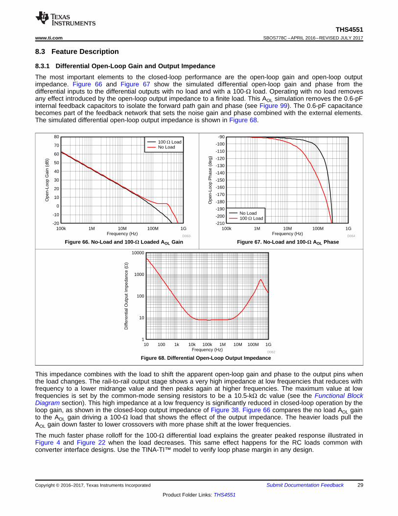
Frequency (Hz)
Diff
eren
tial O
utpu
t Im
peda
nce
(:)
1
10
100
1000
10000
10 100 1k 10k 100k 1M 10M 100M 1G
D062
Frequency (Hz)
Ope
n-Lo
op G
ain
(dB
)
-20
-10
0
10
20
30
40
50
60
70
80
100k 1M 10M 100M 1G
D063
100 : LoadNo Load
Frequency (Hz)
Ope
n-Lo
op P
hase
(de
g)
-210
-200
-190
-180
-170
-160
-150
-140
-130
-120
-110
-100
-90
100k 1M 10M 100M 1G
D064
No Load100 : Load
29
THS4551www.ti.com SBOS778C –APRIL 2016–REVISED JULY 2017
Product Folder Links: THS4551
Submit Documentation FeedbackCopyright © 2016–2017, Texas Instruments Incorporated
8.3 Feature Description
8.3.1 Differential Open-Loop Gain and Output ImpedanceThe most important elements to the closed-loop performance are the open-loop gain and open-loop outputimpedance. Figure 66 and Figure 67 show the simulated differential open-loop gain and phase from thedifferential inputs to the differential outputs with no load and with a 100-Ω load. Operating with no load removesany effect introduced by the open-loop output impedance to a finite load. This AOL simulation removes the 0.6-pFinternal feedback capacitors to isolate the forward path gain and phase (see Figure 99). The 0.6-pF capacitancebecomes part of the feedback network that sets the noise gain and phase combined with the external elements.The simulated differential open-loop output impedance is shown in Figure 68.
Figure 66. No-Load and 100-Ω Loaded AOL Gain Figure 67. No-Load and 100-Ω AOL Phase
Figure 68. Differential Open-Loop Output Impedance
This impedance combines with the load to shift the apparent open-loop gain and phase to the output pins whenthe load changes. The rail-to-rail output stage shows a very high impedance at low frequencies that reduces withfrequency to a lower midrange value and then peaks again at higher frequencies. The maximum value at lowfrequencies is set by the common-mode sensing resistors to be a 10.5-kΩ dc value (see the Functional BlockDiagram section). This high impedance at a low frequency is significantly reduced in closed-loop operation by theloop gain, as shown in the closed-loop output impedance of Figure 38. Figure 66 compares the no load AOL gainto the AOL gain driving a 100-Ω load that shows the effect of the output impedance. The heavier loads pull theAOL gain down faster to lower crossovers with more phase shift at the lower frequencies.
The much faster phase rolloff for the 100-Ω differential load explains the greater peaked response illustrated inFigure 4 and Figure 22 when the load decreases. This same effect happens for the RC loads common withconverter interface designs. Use the TINA-TI™ model to verify loop phase margin in any design.

�
F
VG2
S
T
R2
AR
R1
R
�
�
FS
VG1
S
T
R2 R
AR
R1
R
� � � �( ) ( )
§ ·�¨ ¸
© ¹� � � � � � � �
2SS F V 2
2 F S VT T
F V S V V F V S V V
R2R 2R A
2R R A2R R 0
2R 2 A R A 4 A 2R 2 A R A 4 A
RF1
1 k
RL
1 k
RG1
1 k
RG2
1.02 k
RT
52.3
THS4551 Wideband,Fully Differential Amplifier50- �Input Match,
Gain of 1 V/V from RT, Single-Ended Source to
Differential Output
VOCM
RF2
1 k
50- Source
Impedance
+
±
VS+
+
±
VS+
FDA
PD
VS-
VOPP
RS1
50
Copyright © 2016, Texas Instruments Incorporated
30
THS4551SBOS778C –APRIL 2016–REVISED JULY 2017 www.ti.com
Product Folder Links: THS4551
Submit Documentation Feedback Copyright © 2016–2017, Texas Instruments Incorporated
Feature Description (continued)8.3.2 Setting Resistor Values Versus GainThe THS4551 offers considerable flexibility in the configuration and selection of resistor values. The design startswith the selection of the feedback resistor value. The 1-kΩ feedback resistor value used for the characterizationcurves is a good compromise between power, noise, and phase margin considerations. With the feedbackresistor values selected (and set equal on each side) the input resistors are set to obtain the desired gain withinput impedance also set with these input resistors. Differential I/O designs provide an input impedance that isthe sum of the two input resistors. Single-ended input to differential output designs present a more complicatedinput impedance. Most characteristic curves implement the single-ended to differential design as the morechallenging requirement over differential-to-differential I/O.
For single-ended, matched, input impedance designs, Table 2 illustrates the suggested standard resistors set toapproximately a 1-kΩ feedback. This table assumes a 50-Ω source and a 50-Ω input match and uses a singleresistor on the non-signal input side for gain matching. Better matching is possible using the same three resistorson the non-signal input side as on the input side. Figure 69 shows the element values and naming convention forthe gain of 1-V/V configuration where the gain is defined from the matched input at RT to the differential output.
Figure 69. Single-Ended to Differential Gain of 1 V/V with Input Matching Using Standard Resistor Values
Starting from a target feedback resistor value, the desired input matching impedance, and the target gain (AV),the required input RT value is given by solving the quadratic of Equation 1.
(1)
When this value is derived, the required input side gain resistor is given by Equation 2 and then the single valuefor RG2 on the non-signal input side is given by Equation 3:
(2)
(3)

�OPP
Omin OCMV
V V4
�OPP
Omax OCMV
V V4
§ ·§ ·� �¨ ¸¨ ¸
© ¹© ¹
�
G1 F
G2 G1A G1
F
G2
R R1 1
R RZ R
R2
R
31
THS4551www.ti.com SBOS778C –APRIL 2016–REVISED JULY 2017
Product Folder Links: THS4551
Submit Documentation FeedbackCopyright © 2016–2017, Texas Instruments Incorporated
Feature Description (continued)Using these expressions to generate a swept gain table of values results in Table 2, where the best standard 1%resistor values are shown to minimize input impedance and gain error to target.
Table 2. Swept Gain 50-Ω Input Match with RF = 1-kΩ (±1 Standard Values)GAIN (V/V) RF RG1 RT RG2 ZIN AV
0.1 1000 10000 49.9 10000 49.66 0.099651 1000 976 51.1 1000 49.2 1.00962 1020 499 52.3 523 48.9 1.9885 1000 187 59 215 50.2 5.05710 1020 88.7 69.8 118 50.6 10.09
Where an input impedance match is not required, simply set the input resistor to obtain the desired gain withoutan additional resistor to ground (remove RT in Figure 69). This scenario is common when coming from the outputof another single-ended op amp (such as the OPA192). This single-ended to differential stage shows a higherinput impedance than the physical RG as given by the expression for ZA (active input impedance) shown asEquation 4.
(4)
Using Equation 4 for the gain of 1 V/V with all resistors equal to 1-kΩ shows an input impedance of 1.33 kΩ. Theincreased input impedance comes from the common-mode input voltage at the amplifier pins moving in the samedirection as the input signal. The common-mode input voltage must move to create the current in the non-signalinput RG resistor to produce the inverted output. The current flow into the signal-side input resistor is impededbecause the common-mode input voltage moves with the input signal, thus increasing the apparent inputimpedance in the signal input path.
8.3.3 I/O Headroom ConsiderationsThe starting point for most designs is to assign an output common-mode voltage for the THS4551. For ac-coupled signal paths, this voltage is often the default midsupply voltage to retain the most available output swingaround the voltage centered at the VOCM voltage. For dc-coupled designs, set this voltage with consideration tothe required minimum headroom to the supplies as described in the specifications of the ElectricalCharacteristics table for the VOCM control. For precision ADC drivers, this output VOCM becomes the input VCM tothe ADC. Often, VCM is set to VREF / 2 to center the differential input on the available input when precision ADCsare being driven.
From the target output VOCM, the next step is to verify that the desired output differential peak-to-peak voltage(VOPP) stays within the supplies. For any desired differential VOPP, make sure that the absolute maximum voltageat the output pins swings with Equation 5 and Equation 6 and confirm that these expressions are within thesupply rails minus the output headroom required for the RRO device.
(5)
(6)
For instance, when the THS4551 drives the ADC3223 with a 0.95-VCM control using a single 3.0-V supply, thenegative-going signal sets the maximum output swing from 0.95 VCM to 0.2 V above ground. This 0.75-V, single-sided swing becomes an available 4 × 0.75 V = 3-VPP differential around the nominal 0.95-VCM output common-mode voltage. On the high side, the maximum output is equal to 1.7 V (0.95 V + 0.75 V), which is well within theallowed maximum range of 2.8 V (3.0 V – 0.2 V). This available 3-VPP maximum differential output is also wellbeyond the maximum value required for the 2-VPP input ADS3223.

RF1
1.02 k
RL
1 k
RG1
499
RG2
523
THS4551 Wideband,Fully Differential Amplifier
RF2
1.02 k
Thevinized Source
+
±
VS+
+
±
VOCM
VS+
FDA
PD
VS-
VOUT = 4-VPP
Differential
RS1
25.6
1 µF
1 µF
1 µFVIN = ±1.022 V
+
±
+
±3.3 V 0 V
VS+ VS-
Copyright © 2016, Texas Instruments Incorporated
32
THS4551SBOS778C –APRIL 2016–REVISED JULY 2017 www.ti.com
Product Folder Links: THS4551
Submit Documentation Feedback Copyright © 2016–2017, Texas Instruments Incorporated
With the output headrooms confirmed, the input junctions must also stay within the operating range. The inputrange limitations only appear when approaching the positive supply where a maximum 1.3-V headroom isrequired over the full temperature range because the input range extends to the negative supply voltage over thefull temperature range.
The input pins operate at voltages set by the external circuit design, the required output VOCM, and the inputsignal characteristics. For differential-to-differential designs where there is no signal-related movement in theinput VICM voltages, ac-coupled differential input designs have a VICM equal to the output VOCM. Going towardsthe positive supply, the output common-mode can be set to within 1.2 V of the supply. AC-coupled input designsviolate the required 1.3-V headroom on the input pins in this case. Going towards the negative supply on theVOCM setting requires a minimum of 0.55 V above the supply. This extreme is always in range for the input pinsthat require a minimum 0-V headroom to the negative supply.
DC-coupled differential input designs must check the voltage divider from the source common-mode inputvoltage to the THS4551 VOCM setting. This result must be equal to an input VICM within the specified range. If thesource VCM can vary over some voltage range, validate this result over that range before proceeding.
For single-ended input to differential output designs, the VICM is nominally at a voltage set by the externalconfiguration with a small swing around the nominal value because of the common-mode loop. An ac-coupled,single-ended input to differential output design places an average input VICM equal to the output VOCM for theFDA with an ac-coupled swing around the VOCM voltage following the input voltage. A dc-coupled, single-endedinput to differential design gets a nominal input VICM set by the source signal common-mode level and the VOCMoutput voltage with a small signal-related swing around the nominal VICM voltage.
One approach to deriving the VICM voltage range for any single-ended input to differential output design is toobserve the output voltage swing on the non-signal input side of the FDA outputs and simply take the voltagedivision on the input pin to ground or to the dc reference used on that side. An example analysis is shown inFigure 70 using a Thevenized version of the gain of 2 values listed in Table 2 for a 50-Ω matched impedance,ac-coupled design.
In this example, a single 3.3-V supply is used with the VOCM defaulted to midsupply or 1.65 V as a common-mode output voltage. This value is also the common-mode voltage on the input pins for the ac-coupled input tothe FDA. Targeting a 4-VPP differential output swing means each output pin swings ±1 V around this 1.65-Vcommon-mode voltage. This output swing is in range because the full swing is 0.65 V to 2.65 V relative toground, which is well within the 0.2-V output headroom requirements on a single 3.3-V supply.
Figure 70. Input Swing Analysis Circuit with AC-Coupled, Single-Ended to Differential Signal Path
The output on the lower side of this design ranges from 0.65 V to 2.65 V. This 2-VPP swing (on just one side, theother output is an inverted version and gives the 4-VPP differential maximum) is divided back by the RF2 and RG2divider to the input pins to form a common-mode input swing on top of the 1.65-V input common-mode voltage.This divider is 0.339 × 2 VPP = 0.678 VPP or ±0.34 V around the 1.65-V input common-mode voltage. The 1.31-Vto 1.99-V common-mode input swing for this design is in range for the 0 V to 2.2 V available input range (themaximum headroom is 3.3 V – 1.1 V, which is equal to 2.2 V). These voltage swings can be directly observedusing the SBOC460 TINA-TI™ simulation file. Shifting the VOCM down slightly (if allowed by the designrequirements) is a good way to improve the positive-swinging input headroom for this low-voltage design.

RF1
1 k
RL
1 k
RG1
4.99 k
RG2
4.99 k
THS4551 Wideband,Fully Differential Amplifier
Gain of 0.2 V/V,DC-Coupled,
Single-Ended Source to Differential Output
VOCM
RF2
1 k
+
±
VS+
+
±
VS+
FDA
PD
VS-
10 k
10 k
+
±
+
±
+
±
1 µF
2.6 pF
VOCM
5 V 0 V
4.096 V
3.1 pF
3.1 pF
VOUT = 7.2 VPP
Differential
VS = ±18 VVS+ VS-
For Attenuator Design:NG1 = 1.2NG2 = 3GBP = 135 MHzZo = 14.3 MHz
A 1-k �load is veryimportant to include because of high-frequency resonance;
no load may oscillate.
Copyright © 2016, Texas Instruments Incorporated
33
THS4551www.ti.com SBOS778C –APRIL 2016–REVISED JULY 2017
Product Folder Links: THS4551
Submit Documentation FeedbackCopyright © 2016–2017, Texas Instruments Incorporated
Taking a more complex example by using the THS4551 to attenuate a large bipolar input signal in a dc-coupleddesign for an ADC is shown in Figure 71. To remove the peaking for this low-noise gain design, the two CFelements and an input capacitor are added to shape the noise gain at high frequencies to a capacitive divider, asdescribed in the Designing Attenuators section. In this example (including the 1.2-pF internal differential capacitorat the inputs and the 0.6-pF internal feedback capacitors), the high-frequency noise gain is 3 V/V and a flatfrequency response with approximately 45 MHz of –3-dB BW is delivered.
Figure 71. DC-Coupled, Single-Ended to Differential Attenuator Design
In this example, the output VOCM is 4.096 V / 2, which equals 2.048 V and the source signal VCM is 0 V. Thesevalues set the nominal input pin VICM to 2.048 V × 4.99 kΩ / (4.99 kΩ + 1 kΩ) = 1.71 V. Applying a ±18-V input atthe 4.99-kΩ input resistor produces a 7.2-VPP differential output. That is, a ±1.8-V swing on the lower output sidearound the 2.048-V common-mode voltage. This 0.248-V to 3.84-V relative-to-ground swing at the output is wellwithin the 0.2-V output headrooms to the 0-V to 5-V supplies used in the example in Figure 71 (with the sameswing inverted on the other output side). That output swing on the lower side produces an attenuated inputcommon mode swing of (±1.8 V × (4.99 kΩ / (4.99 kΩ + 1 kΩ)) = ±1.5 V around the midscale input bias of1.71 V. This 0.2-V to 3.2-V input common-mode swing is well within the available 0-V to 3.8-V input range. This±18-V bipolar input signal is delivered to a SAR ADC with a 7.2-VPP differential output with all I/O nodesoperating in range using a single 5-V supply design. The source must sink the 2.048 V / 5.99 kΩ = 0.34-mAcommon-mode level-shifting current to take the input 0-V common-mode voltage up to the midscale 1.71-V VICMoperating voltage. Using the single-ended input impedance of Equation 4, the source must also drive anapparent input load of 5.44 kΩ.
Most designs do not run into an input range limit. However, using the approach shown in this section can allow aquick assessment of the input VICM range under the intended full-scale output condition. The TINA-TI™simulation file for Figure 71 can be used to plot the input voltages under the intended swings and applicationcircuit to verify that there is no limiting from this effect. Driving the I/O nodes out of range in the TINA-TI™ modelresults in convergence problems. Increasing the positive and negative supplies slightly in simulation is an easyway to discover the simulated swings that might be going out of range.

r u
� �
G THEV FICM OCM
G F F G
R V RV V
R R 2 R R
RF1
1 k
RL
1 k
R2215
R2215
THS4551 Wideband,Fully Differential Amplifier
VOCM
RF2
1 k
+
±
VS+
+
±
VS+
FDA
PD
VS-
VOUT
Thevinized Source
+
±
+
±
3.3 V 0 V
VS+ VS-
VTHEV
±0.217 V
+
±
VOCM
0.95 V
±1-V Differential Output Centered on 0.95 VCM
Copyright © 2016, Texas Instruments Incorporated
34
THS4551SBOS778C –APRIL 2016–REVISED JULY 2017 www.ti.com
Product Folder Links: THS4551
Submit Documentation Feedback Copyright © 2016–2017, Texas Instruments Incorporated
As a third example of arriving at the input pin voltage swings, use the design of Figure 93 (the ADC3241 design).Thevenize the source to just one input resistor to get an expression for the input VICM in terms of the inputvoltage to be derived. Figure 72 shows the gain of 5 V/V, dc-coupled, matched input impedance, single-ended todifferential circuit of Figure 93 with both sides reduced to a single input resistor. In Figure 93, the design operateson a single 3.3-V supply with an output VOCM equal to 0.95 V to directly connect to TI’s line of low-powerADC3xxx series of 12- and 14-bit ADCs. This family accepts a 2-VPP maximum differential voltage, which (at theinput-terminating resistor of Figure 93) is a ±0.2-V swing. Going back to the source through the matching resistoris then a ±0.4-V source swing. Thevenizing that source with the RT element provides the ±0.217 V shown inFigure 72 and the total R2 as the sum of RG1 and 50 Ω || 59 Ω.
Figure 72. Input VICM Analysis Circuit From the Design of Figure 93
For an input signal (VTHEV) that swings around ground as ±VTHEV, the input pins are within a range given byEquation 7, which is a superposition of the output VOCM divided back to the input nodes and half of the input±VTHEV signal.
(7)
Using the values from the design of Figure 72, the computed input range for the THS4551 input pins is VICM =0.168 V ± 0.89 mV or 0.079 V to 0.257 V at the input pins. These values are well within range for the negativerail input available in the THS4551.
A simpler approach to arriving at the input common mode range for this DC coupled single supply design wouldbe to take the output voltage swing range on the lower side (non – signal input side) and simply divide it backthrough its resistor divider to ground on that side.

Time (ns)
Out
put (
V)
0 100 200 300 400 500 600 700 800 900 1000-1.2
-1
-0.8
-0.6
-0.4
-0.2
0
0.2
0.4
0.6
0.8
1
1.2
D069
VIN+VOUTVS
35
THS4551www.ti.com SBOS778C –APRIL 2016–REVISED JULY 2017
Product Folder Links: THS4551
Submit Documentation FeedbackCopyright © 2016–2017, Texas Instruments Incorporated
The output pin voltage swing is 0.95 V ± 0.5 V or 0.45 V to 1.45 V. This swing is divided back to the input VICMby a 215 / (215 + 1000) = 0.177 ratio. This ratio computes the input pin range as 79 mV to 0.256 V, matching theinput source swing results in Equation 7. The TINA-TI™ model for Figure 72 (available as SBOC472) alsoprovides these input swings as shown in the simplified circuit of Figure 73. The large centered swing is thedifferential output voltage at the THS4551 output pins (which is actually the two outputs swinging ±0.5 V arounda 0.95 VCM), the small centered bipolar swing is the input swing for the thevenized source of Figure 73, and thesmallest VPP swing on a dc offset is the input VICM voltage at the non-signal side input for the circuit of Figure 73.
Figure 73. I/O Swing Simulation Using the TINA-TI™ Model
8.3.4 Output DC Error and Drift Calculations and the Effect of Resistor ImbalancesThe THS4551 offers a trimmed input offset voltage and extremely low offset drift over the full –40°C to +125°Coperating range. This offset voltage combines with several other error contribution terms to produce an initial25°C output offset error band and then a drift over temperature. For each error term, a gain must be assigned tothat term. For this analysis, only dc-coupled signal paths are considered. One new source of output error (versusthe typical op amp analysis) arises from the effect mismatched resistor values and ratios can have on the twosides of the FDA. Any common-mode error or drift creates a differential output error through the slightmismatches arising from the external feedback and gain setting resistor tolerances or standard value constraints.
The error terms (25°C and drift), along with the gain to the output differential voltage, include input offset voltageand input offset current. Input offset voltage has a gain equal to the noise gain or 1 + RF / RG, where RG is thetotal dc impedance from the input pins back to the source or a dc reference (typically ground). Input offset currenthas a gain to the differential output through the average feedback resistor value.
The remaining terms arise from an assumed range on both the absolute feedback resistor mismatch and themismatch in the divider ratio on each side of the FDA. The first of these resistor mismatch terms is the input biascurrent that creates a differential output offset via RF mismatch. For simplicity, the upper RF and RG values aretermed RF1 and RG1 with a ratio of RF1 / RG1 ≡ G1. The lower elements are defined as RF2 and RG2 with a ratio ofRF2 / RG2 ≡ G2. To compute worst-case contributions, a maximum variation in the design resistor tolerance isused in the absolute and ratio mismatches.
For instance, ±1% tolerance resistors are assumed, giving a worst-case G1 that is 2% higher than nominal and aG2 that is 2% lower than nominal with a worst-case RF value mismatch of 2% as well. Using a 0.1% precisionresistor reduces the gain for the input bias current, but because these precision resistors are usually onlyavailable in 1% value steps, a gain mismatch term may still need to be considered. For matched impedancedesigns with RT and RG1 on a single-ended to differential stage, the standard value constraint imposes a fixedmismatch in the initial feedback ratios with the tolerance of the resistors around the ratio if the non-signal inputside uses a single resistor for RG2.
Define the selected external resistor tolerance as ±T (so for 1% tolerance resistors, T = 0.01). Input bias currenttimes the feedback resistor mismatch gain is ±2 × T × RFnom.
Anything that generates an output common-mode level or shift over temperature also generates an outputdifferential error term if the two feedback ratios, G1 and G2, are not equal. An error trying to produce a shift inthe output common-mode voltage is overridden by the common-mode control loop where the error becomes abalanced differential error around the output VOCM.

RF1
1 k
RL
1 k
RG1
1 k
RG2
1.02 k
RT1
52.3
THS4551 Wideband,Fully Differential Amplifier50- �Input Match,
Gain of 1 V/V from RT, Single-Ended Source to
Differential Output
VOCM
RF2
1 k
50- Source
Impedance
+
±
VS+
+
±
VS+
FDA
PD
VS-
VOPP
RS1
50
+
±
+
±5 V 0 V
VS+ VS-
+
±2.5 V
VOCM
Copyright © 2016, Texas Instruments Incorporated
�
( ) ( )
� �
OD2
OCM
V G 4V 1 G 1
T
T
� � � �� � �
��
OCM ICMOD
V G1 G2 V G1 G2V
G1 G21
2
36
THS4551SBOS778C –APRIL 2016–REVISED JULY 2017 www.ti.com
Product Folder Links: THS4551
Submit Documentation Feedback Copyright © 2016–2017, Texas Instruments Incorporated
The terms that create a differential error from a common-mode term and feedback ratio mismatch include thedesired VOCM voltage, any source common-mode voltage, any drift on the reference bias to the VOCM control pin,any internal offset and drift in the VOCM control path, and the input average bias current and drift.
Considering just the output common-mode control and the source common-mode voltage, the conversion tooutput differential offsets is through Equation 8.
(8)
Neglecting any G1 and G2 mismatch because of standard values constraint, the conversion gain for these twoterms can be recast in terms of the nominal RF / RG ≡ G and the tolerance T, as shown in Equation 9. When Gincreases, this conversion gain approaches 4T.
(9)
This conversion gain to differential output error is applied to two error terms: VOCM and the input bias current anddrift. (The source common-mode voltage is assumed to be 0 V. If not, apply this gain to the source common-mode voltage and any resulting shift in application.)
The output error is applied to VOCM, assuming that the input control pin is driven and not floating. The input biascurrent and drift are multiplied by the average RF value then by the conversion gain to differential output error tocreate an added output differential error.
As an example of using these terms to estimate the worst-case output 25°C error band and then the worst-casedrift (by adding all error terms together independently), use the gain of 1-V/V configuration with RF = 1 kΩ andassume a ±1% tolerance on the resistors with the standard values used in Figure 74.
Figure 74. DC-Coupled Gain of 1 with RF = 1 kΩ and Single-to-Differential Matched Input 50-Ω Impedance
The standard value constraint on the non-signal input side actually produces more gain mismatch than theresistor tolerances. For Figure 74, G2 = 1000 / 1020 = 0.9804 and G1 = 1000 / 1025.6 = 0.9751 nominally, thenwith a ±2% tolerance around the initial gain mismatch resulting from the standard values available if 1% resistorsare used.
Using the maximum 25°C error terms and nominal resistor values with an exact 2.5-V input to the VOCM controlpin gives Table 3, gains to the output differential error (VOD), and then the summed output error band at 25°C.The output error is clearly dominated by the VOCM voltage and the effect of the nominal feedback dividers beingslightly mismatched. This analysis does not include resistor tolerances but the approach is the same with thewider error bands on the gain terms. Using 1% tolerance on the resistors setting the gain matching dominatesthe output error band through the VOCM input voltage. For the lowest output error, this analysis shows that anexact match on the feedback dividers with precision resistors is preferred. However, doing so would requireduplicating the exact network on the non-signal input side and the signal input side. Where input impedancematching is not required, the two RG resistors are simply single equal resistors and the gain mismatch is justfrom the tolerance of the resistors.

37
THS4551www.ti.com SBOS778C –APRIL 2016–REVISED JULY 2017
Product Folder Links: THS4551
Submit Documentation FeedbackCopyright © 2016–2017, Texas Instruments Incorporated
Table 3. Worst-Case Output VOD Error Band
ERROR TERM 25°C MAX VALUE GAIN TO VODOUTPUT ERROR
(mV) GAIN COMMENT
Input VIO ±0.175 mV 1.9777 ±0.346 Average noise gainInput IOS ±50 nA 1000 ±0.05 Feedback resistor
Input IBCM 1.5 µA 20 Ω ±0.03 Feedback resistor mismatchInput IBCM 1.5 µA 1 kΩ × 0.00268 ±0.004 Converted to differential by gain mismatchVOCM input 2.5 V 0.00268 ±6.7 VOCM to differential by gain mismatch
Total ±7.13
The 0.00268 conversion gain for the gain ratio mismatch is the worst-case ratio starting from the initially lowerG1 value resulting from the standard value constraint and using a ±1% tolerance on the RF and RG elements ofthe ratio. Adding in the resistor tolerances to the gain mismatch term greatly increases the contribution of thoseterms.
Normally, the expected drift in the output VOD is of more interest than an initial error band. Table 4 shows theseterms for the RGT package and the summed results by adding all terms independently to obtain a worst-casedrift.
Table 4. Worst-Case Output VOD Drift Band
ERROR TERM MAX VALUE GAIN TO VODOUTPUT ERROR
(µV/°C) GAIN COMMENT
Input VIO ±1.8 µV/°C 1.9777 ±3.56 Average noise gainInput IOS ±120 pA/°C 1000 ±0.12 Feedback resistor
Input IBCM 5.0 nA/°C 20 Ω ±0.10 Feedback resistor mismatchInput IBCM 5.0 nA/°C 1 kΩ × 0.00268 ±0.013 Converted to differential by gain mismatchVOCM input ±10 µV/°C 0.00268 ±0.027 VOCM to differential by gain mismatch
Total ±3.82
In Table 4, the input offset voltage drift dominates the output drift. For the last term, the drift for the VOCM path isjust for the internal offset drift of the common-mode path with a driven input. Any added external drift on thesource of the VOCM input must also be considered. This type of calculation can be repeated for the exactapplication circuit considering each of these terms in the context of a specific design.
The absolute accuracy and drift for the THS4551 are exceptionally good. Mismatched resistor feedback ratioscombined with a high drift in the VOCM control input can actually dominate the output VOD drift. Where the outputdifferential precision is more important than the input matching accuracy, consider matching the networks on thetwo sides of the input to obtain improved nominal G1 to G2 match. The gains for the input bias current errorterms are relatively low when using the 1-kΩ feedback values. Higher RF values provide the input-current-relateddrift terms more gain.

38
THS4551SBOS778C –APRIL 2016–REVISED JULY 2017 www.ti.com
Product Folder Links: THS4551
Submit Documentation Feedback Copyright © 2016–2017, Texas Instruments Incorporated
8.4 Device Functional ModesThe wideband FDA requires external resistors for correct signal-path operation. When configured for the desiredinput impedance and gain setting with these external resistors, the amplifier can be either on with the PD pinasserted to a voltage greater than (VS–) + 1.15 V, or turned off by asserting PD low (within 0.55 V of the negativesupply). Disabling the amplifier shuts off the quiescent current and stops correct amplifier operation. The signalpath is still present for the source signal through the external resistors, which provides poor signal isolation fromthe input to output in power-down mode.
Internal protection diodes remain present across the input pins in both operating and shutdown mode. Largeinput signals during disable can turn on the input differential protection diodes, thus producing a load current inthe supply even in shutdown.
The VOCM control pin sets the output average voltage. Left open, VOCM defaults to an internal midsupply value.Driving this high-impedance input with a voltage reference within the valid range sets a target for the internal VCMerror amplifier. If floated to obtain a default midsupply reference for VOCM, an external decoupling capacitor isrecommended to be added on the VOCM pin to reduce the otherwise high output noise for the internal high-impedance bias (see Figure 45).
8.4.1 Operation from Single-Ended Sources to Differential OutputsOne of the most useful features supported by the FDA device is an easy conversion from a single-ended input toa differential output centered on a user-controlled, common-mode level. Although the output side is relativelystraightforward, the device input pins move in a common-mode manner with the input signal. The common-modevoltage at the input pins, which moves with the input signal, increases the apparent input impedance to begreater than the RG value. The input active impedance issue applies to both ac- and dc-coupled designs, andrequires somewhat more complex solutions for the resistors to account for this active impedance, as discussed inthe Setting Resistor Values Versus Gain section.
8.4.1.1 AC-Coupled Signal Path Considerations for Single-Ended Input to Differential OutputConversions
When the signal path can be ac-coupled, the dc biasing for the THS4551 becomes a relatively simple task. In alldesigns, start by defining the output common-mode voltage. The ac-coupling issue can be separated for theinput and output sides of an FDA design. The input can be ac-coupled and the output dc-coupled, or the outputcan be ac-coupled and the input dc-coupled, or both can be ac-coupled. One situation where the output can bedc-coupled (for an ac-coupled input), is when driving directly into an ADC where the VOCM control voltage usesthe ADC common-mode reference to directly bias the FDA output common-mode voltage to the required ADCinput common-mode voltage. In any case, the design starts by setting the desired VOCM. When an ac-coupledpath follows the output pins, the best linearity is achieved by operating VOCM at midsupply, which can be easilydelivered by floating the VOCM pin. The VOCM voltage must be within the linear range for the common-modeloop, as specified in the headroom specifications (approximately 0.7 V greater than the negative supply and1.3 V less than the positive supply for the full –40°C to +125°C operation). If the output path is also ac-coupled,simply letting the VOCM control pin float is usually preferred in order to obtain a midsupply default VOCM bias withminimal elements. To limit noise, place a 0.1-µF decoupling capacitor on the VOCM control pin to ground.
After VOCM is defined, check the target output voltage swing to ensure that the VOCM plus the positive andnegative output swing on each side does not clip into the supplies. If the desired output differential swing isdefined as VOPP, divide by 4 to obtain the ±VP (peak voltage) swing around VOCM at each of the two output pins(each pin operates 180° out of phase with the other). Check that VOCM ±VP does not exceed the absolute supplyrails for the rail-to-rail output (RRO) device. Common-mode current does not flow from the common-mode outputvoltage set by the VOCM pin towards the device input pins side, because both the source and balancing resistoron the non-signal input side are dc blocked (see Figure 70). The ac-coupled input path sets the input pincommon-mode voltage equal to the output common-mode voltage. The input pin positive headroom requirement(1.2 V) is less than the VOCM positive headroom (1.3 V). If the VOCM is in range, the input pins are also in rangefor the ac-coupled input configuration. This headroom requirement functions similarly for when the output VOCMvoltage approaches the negative supply. The approximate minimum headroom of 0.6 V to the negative supply onthe VOCM voltage is greater than the input pin voltage headroom of approximately 0 V for the negative rail inputdesign. The input common-mode voltage is also in range if the output common-mode voltage is in range andabove 0.6 V from the negative supply because the input common-mode voltage follows the output VOCM settingfor ac-coupled input designs.

39
THS4551www.ti.com SBOS778C –APRIL 2016–REVISED JULY 2017
Product Folder Links: THS4551
Submit Documentation FeedbackCopyright © 2016–2017, Texas Instruments Incorporated
Device Functional Modes (continued)The input pin voltages move in a common-mode manner with the input signal, as described in the I/O HeadroomConsiderations section. Confirm that the VOCM voltage plus the input VPP common-mode swing also stays inrange for the input pins.
8.4.1.2 DC-Coupled Input Signal Path Considerations for Single-Ended to Differential ConversionsThe output considerations remain the same as for the ac-coupled design. Again, the input can be dc-coupledwhen the output is ac coupled. A dc-coupled input with an ac-coupled output can have some advantages tomove the input VICM down by adjusting the VOCM down if the source is ground referenced. When the source is dc-coupled into the THS4551 (see Figure 69), both sides of the input circuit must be dc-coupled to retain differentialbalance. Normally, the non-signal input side has an RG element biased to whatever the source midrange isexpected to be, provided that this midscale reference gives a balanced differential swing around VOCM at theoutputs. Often, RG2 is simply grounded for dc-coupled, bipolar-input applications. This configuration provides abalanced differential output if the source swings around ground. If the source swings from ground to somepositive voltage, grounding RG2 gives a unipolar output differential swing from both outputs at VOCM (when theinput is at ground) to one polarity of the swing. Biasing RG2 to an expected midpoint for the input signal creates adifferential output swing around VOCM.
One significant consideration for a dc-coupled input is that VOCM sets up a common-mode bias current from theoutput back through RF and RG to the source on both sides of the feedback. Without input balancing networks,the source must sink or source this dc current. After the input signal range and biasing on the other RG elementis set, check that the voltage divider from VOCM to VIN through RF and RG (and possibly RS) establishes an inputVICM at the device input pins that is in range. If the average source is at ground, the negative rail input stage forthe THS4551 is in range for applications using a single positive supply and a positive output VOCM settingbecause this dc common-mode current lifts the average FDA input summing junctions up off of ground to apositive voltage (the average of the V+ and V– input pin voltages on the FDA). TINA-TI™ simulations of theintended circuit offer a good check for input and output pin voltage swings (see Figure 72).
8.4.2 Operation from a Differential Input to a Differential OutputIn many ways, this method is a much simpler way to operate the FDA from a design equations perspective.Again, assuming that the two sides of the circuit are balanced with equal RF and RG elements, the differentialinput impedance is now just the sum of the two RG elements to a differential inverting summing junction. In thesedesigns, the input common-mode voltage at the summing junctions does not move with the signal but must be dcbiased in the design range for the input pins and must take into account the voltage headroom required to eachsupply. Slightly different considerations apply to ac- or dc-coupled differential input to differential output designs,as described in the following sections.

RF1
1.02 k
RL
1 k
RG1
499
RG2
499
THS4551 Wideband,Fully Differential Amplifier
RF2
1.02 k
Differential I/O with AC-Coupled
Input
+
±
VS+
+
±
VOCM
VS+
FDA
PD
VS-
VOUT
10 nF
10 nF
1 µFVIN
+
±
+
±3.3 V 0 V
VS+ VS-
RF1
1.02 k
Copyright © 2016, Texas Instruments Incorporated
40
THS4551SBOS778C –APRIL 2016–REVISED JULY 2017 www.ti.com
Product Folder Links: THS4551
Submit Documentation Feedback Copyright © 2016–2017, Texas Instruments Incorporated
Device Functional Modes (continued)8.4.2.1 AC-Coupled, Differential-Input to Differential-Output Design IssuesThe most common way to use the THS4551 with an ac-coupled differential source is to simply couple the inputinto the RG resistors through the blocking capacitors. Figure 75 shows a typical blocking capacitor approach to adifferential input. An optional input differential termination resistor (RM) is included in this design. The RM elementallows the input RG resistors to be scaled up and still delivers lower differential input impedance to the source. Inthis example, the RG elements sum to show a 1-kΩ differential impedance and the RM element combines inparallel to provide a net 500-Ω ac differential impedance to the source. Again, the design ideally proceeds byselecting the RF element values, then the RG to set the differential gain, and then an RM element (if needed) toachieve a target input impedance. Alternatively, the RM element can be eliminated, with the 2 × RG elements setto the desired input impedance and RF set to obtain the differential gain (equal to RF / RG).
Figure 75. Example AC-Coupled Differential Input Design
The dc biasing for an ac-coupled differential input design is very simple. The output VOCM is set by the inputcontrol voltage and, because there is no dc current path for the output common-mode voltage (as long as RM isonly differential and not split and connected to ground for instance), the dc bias also sets the common-modeoperating points for the input pins. For a purely differential input, the voltages on the input pins remain fixed atthe output VOCM setting and do not move with the input signal (unlike the single-ended input configurations wherethe input pin common-mode voltages do move with the input signal). The SLOC341 TINA-TI™ simulation file isavailable for Figure 75.

RF1
1 k RG1
4.99 k
RG2
4.99 k
THS4551 Wideband,Fully Differential Amplifier
Gain of 0.2 V/V,DC-Coupled,
Differential Input to Differential Output
VOCM
RF2
1 k
+
±
VS+
+
±
VS+
FDA
PD
VS-
10 k
10 k
+
±
+
±
+
±
1 µF
49 pF
VOCM
5 V 0 V
4.096 V
22 pF
22 pF
VS+ VS-
10
10
12 nF
+
±
+
±
OPA2192
2 k
200
2 k
+
±
+
±
-15 V15 V
VEEVCC
VIN1
VIN2
VCC
VEE
VCC
VEE
Copyright © 2016, Texas Instruments Incorporated
ADS9110 Inputs
2.048 V
41
THS4551www.ti.com SBOS778C –APRIL 2016–REVISED JULY 2017
Product Folder Links: THS4551
Submit Documentation FeedbackCopyright © 2016–2017, Texas Instruments Incorporated
Device Functional Modes (continued)8.4.2.2 DC-Coupled, Differential-Input to Differential-Output Design IssuesOperating the THS4551 with a dc-coupled differential input source is very simple and only requires that the inputpins stay in range for the dc common-mode operating voltage. The example in Figure 76 takes the output of adual precision op amp (such as the OPA2192) where a high differential input signal is attenuated by theTHS4551 down into the range of an 18-bit SAR ADC such as the 2-MSPS ADS9110. The input stage provides adifferential gain of 21 V/V with a common-mode gain of 1 V/V. This example amplifies a small differential signalon top of a very-wide range common-mode voltage. The input common-mode voltage appears at the outputs ofthe OPA2192. The input common-mode voltage is level shifted by the FDA common-mode control to be at therequired output common-mode voltage to drive the ADS9110 SAR ADC (with a 4.096-V reference, as shown inFigure 76); the FDA output common-mode voltage must be at the 2.048 V shown in Figure 76. This design offersa very high CMRR using the common-mode control loop of the FDA to reset the output common-mode voltagefrom that delivered to the inputs of the OPA2192. The actual CMRR from the OPA2192 inputs to the FDAoutputs is dominated by the resistor mismatches in the FDA. The feedback and differential input capacitors areincluded to shape the noise gain as described in the Designing Attenuators section. This full example circuit isavailable as a TINA-TI™ simulation file.
Figure 76. Example DC-Coupled Differential I/O Design from a Precision Dual Op Amp to an 18-Bit SAR
8.4.3 Input Overdrive PerformanceFigure 12 illustrates a 2X overdrive triangle waveform for the THS4551. The input resistor is driven with a ±9-Vswing for the gain of 2-V/V configuration in the test circuit of Figure 61 using a single 5-V supply. When theoutput maximum swing is reached at approximately the supply values, the increasing input voltage turns on theinternal protection diodes across the two input pins. The internal protection diodes are two diodes in series inboth polarities. This feature clamps the maximum differential voltage across the inputs to approximately 1.5 Vwhen the output is limited at the supplies but the input exceeds the available range. The input resistors on bothsides limit the current flow in the internal diodes under these conditions.

� � � � � �2 2
o ni N F Fe e NG 2 i R 2 4kTR NG � �
+
±
In+2
In±2
eno2
r
RFRGr
r
RFRG
r
enRg2 enRf
2
enRg2 enRf
2
eni2
42
THS4551SBOS778C –APRIL 2016–REVISED JULY 2017 www.ti.com
Product Folder Links: THS4551
Submit Documentation Feedback Copyright © 2016–2017, Texas Instruments Incorporated
9 Application and Implementation
NOTEInformation in the following applications sections is not part of the TI componentspecification, and TI does not warrant its accuracy or completeness. TI’s customers areresponsible for determining suitability of components for their purposes. Customers shouldvalidate and test their design implementation to confirm system functionality.
9.1 Application InformationMost applications for the THS4551 strive to deliver the best dynamic range in a design that delivers the desiredsignal processing along with adequate phase margin for the amplifier itself. The following sections detail some ofthe design issues with analysis and guidelines for improved performance.
9.1.1 Noise AnalysisThe first step in the output noise analysis is to reduce the application circuit to the simplest form with equalfeedback and gain setting elements to ground. Figure 77 shows the simplest analysis circuit with the FDA andresistor noise terms to be considered.
Figure 77. FDA Noise Analysis Circuit
The noise powers are shown in Figure 77 for each term. When the RF and RG (or RI) terms are matched on eachside, the total differential output noise is the root sum squared (RSS) of these separate terms. Using NG ≡ 1 +RF / RG, the total output noise is given by Equation 10. Each resistor noise term is a 4kT × R power (4kT = 1.6E-20J at 290K).
(10)
The first term is simply the differential input spot noise times the noise gain, the second term is the input currentnoise terms times the feedback resistor (and because there are two uncorrelated current noise terms, the poweris two times one of them), and the last term is the output noise resulting from both the RF and RG resistors, atagain twice the value for the output noise power of each side added together. Running a wide sweep of gainswhen holding RF close to 1 kΩ and setting the input up for a 50-Ω match gives the standard values and resultingnoise listed in Table 5.
Note that when the gain increases, the input-referred noise approaches only the gain of the FDA input voltagenoise term at 3.3 nV/√Hz.

43
THS4551www.ti.com SBOS778C –APRIL 2016–REVISED JULY 2017
Product Folder Links: THS4551
Submit Documentation FeedbackCopyright © 2016–2017, Texas Instruments Incorporated
Application Information (continued)Table 5. Swept Gain of the Output- and Input-Referred Spot Noise Calculations
GAIN (V/V) RF RG1 RT RG2 ZIN AV EO (nV/√Hz) EI (nV/√Hz)0.1 1000 10000 49.9 10000 49.66 0.09965 7 701 1000 976 51.1 1000 49.2 1.0096 10.4 10.42 1020 499 52.3 523 48.9 1.988 13.9 6.955 1000 187 59 215 50.2 5.057 23 4.610 1020 88.7 69.8 118 50.6 10.09 36.4 3.64
9.1.2 Factors Influencing Harmonic DistortionAs illustrated in the swept frequency harmonic distortion plots (Figure 13 and Figure 31), the THS4551 providesextremely low distortion at lower frequencies. In general, an FDA output harmonic distortion mainly relates to theopen-loop linearity in the output stage corrected by the loop gain at the fundamental frequency. When the totalload impedance decreases, including the effect of the feedback resistor elements in parallel for loading purposes,the output stage open-loop linearity degrades, thus increasing the harmonic distortion; see Figure 16 andFigure 34. When the output voltage swings increase, very fine scale open-loop output stage nonlinearitiesincrease that also degrade the harmonic distortion; see Figure 14 and Figure 32. Conversely, decreasing thetarget output voltage swings drops the distortion terms rapidly. A nominal swing of 2 VPP is used for harmonicdistortion testing where Figure 14 illustrates the effect of going up to an 8-VPP differential input that is morecommon with SAR converters.
Increasing the noise gain functions to decrease the loop gain resulting in the increasing harmonic distortionterms; see Figure 18 and Figure 36. One advantage to the capacitive compensation for the attenuator designs isthat the noise gain is shaped up with frequency to achieve a crossover at an acceptable phase margin at higherfrequencies. This technique (see the Designing Attenuators section) holds the loop gain high at frequencieslower than the noise gain zero, thus improving distortion at lower frequencies.
The THS4551 holds nearly constant distortion when the VOCM operating point is moved in the allowed range; seeFigure 17 and Figure 35. Clipping into the supplies with any combination of VOCM and VOPP rapidly degradesdistortion performance.
The THS4551 does an exceptional job of converting from single-ended inputs to differential outputs with very lowharmonic distortions. External resistors of 1% tolerance are used in characterization with good results.Unbalancing the feedback divider ratios does not degrade distortion directly. Imbalanced feedback ratios convertcommon-mode inputs to a differential mode at the outputs with the gain described in the Output DC Error andDrift Calculations and the Effect of Resistor Imbalances section.
9.1.3 Driving Capacitive LoadsThe capacitive load of an ADC or some other next-stage device is commonly required to be driven. Directlyconnecting a capacitive load to the output pins of a closed-loop amplifier such as the THS4551 can lead to anunstable response; see the step response plots into a capacitive load (Figure 8, Figure 10, Figure 26, andFigure 28). One typical remedy to this instability is to add two small series resistors (RO) at the outputs of theTHS4551 before the capacitive load. Figure 6 and Figure 24 illustrate parametric plots of recommended ROvalues versus differential capacitor load values and gains. Operating at higher noise gains requires lower ROvalues to obtain a ±0.5-dB flat response for the same capacitive load. Some direct parasitic loading is acceptablewithout a series RO that increases with gain setting (see Figure 8, Figure 10, Figure 26, and Figure 28 where theRO value is 0 Ω). Even when these plots suggest that a series RO is not required, good practice is to leave aplace for the RO elements in a board layout (a 0-Ω value initially) for later adjustment in case the responseappears unacceptable.
The rail-to-rail output stage of the THS4551 has an inductive characteristic in the open-loop output impedance athigher frequencies; see Figure 68. This inductive open-loop output impedance introduces added phase shift atthe output pins for direct capacitive loads and feedback capacitors. Larger values of feedback capacitors (greaterthan 100 pF) can risk a low phase margin. Including a 10-Ω to 15-Ω series resistor with a feedback capacitor canbe used to reduce this effect.
The TINA-TI™ simulation model does a good job of predicting these issues and illustrating the effect for differentchoices of capacitive load isolating resistors (RO) and different feedback capacitor configurations.
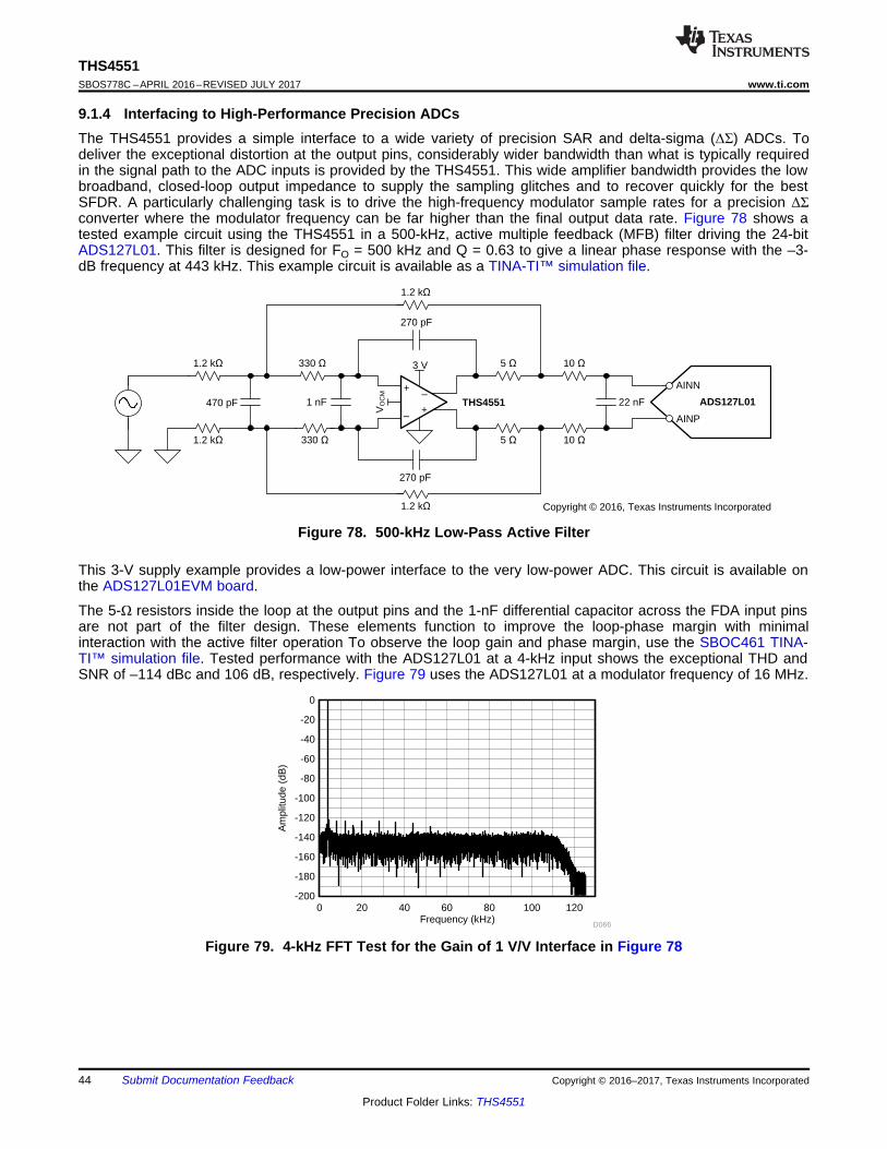
Frequency (kHz)
Am
plitu
de (
dB)
0 20 40 60 80 100 120-200
-180
-160
-140
-120
-100
-80
-60
-40
-20
0
D066
AINN
AINP
ADS127L0122 nF+
±
+±
270 pF
270 pF
VO
CM
1.2 k
1.2 k
5 10
10 5 330 1.2 k
1.2 k 330
THS4551470 pF
Copyright © 2016, Texas Instruments Incorporated
3 V
1 nF
44
THS4551SBOS778C –APRIL 2016–REVISED JULY 2017 www.ti.com
Product Folder Links: THS4551
Submit Documentation Feedback Copyright © 2016–2017, Texas Instruments Incorporated
9.1.4 Interfacing to High-Performance Precision ADCsThe THS4551 provides a simple interface to a wide variety of precision SAR and delta-sigma (ΔΣ) ADCs. Todeliver the exceptional distortion at the output pins, considerably wider bandwidth than what is typically requiredin the signal path to the ADC inputs is provided by the THS4551. This wide amplifier bandwidth provides the lowbroadband, closed-loop output impedance to supply the sampling glitches and to recover quickly for the bestSFDR. A particularly challenging task is to drive the high-frequency modulator sample rates for a precision ΔΣconverter where the modulator frequency can be far higher than the final output data rate. Figure 78 shows atested example circuit using the THS4551 in a 500-kHz, active multiple feedback (MFB) filter driving the 24-bitADS127L01. This filter is designed for FO = 500 kHz and Q = 0.63 to give a linear phase response with the –3-dB frequency at 443 kHz. This example circuit is available as a TINA-TI™ simulation file.
Figure 78. 500-kHz Low-Pass Active Filter
This 3-V supply example provides a low-power interface to the very low-power ADC. This circuit is available onthe ADS127L01EVM board.
The 5-Ω resistors inside the loop at the output pins and the 1-nF differential capacitor across the FDA input pinsare not part of the filter design. These elements function to improve the loop-phase margin with minimalinteraction with the active filter operation To observe the loop gain and phase margin, use the SBOC461 TINA-TI™ simulation file. Tested performance with the ADS127L01 at a 4-kHz input shows the exceptional THD andSNR of –114 dBc and 106 dB, respectively. Figure 79 uses the ADS127L01 at a modulator frequency of 16 MHz.
Figure 79. 4-kHz FFT Test for the Gain of 1 V/V Interface in Figure 78

RF1
1 k
RL
1 k
RG1
10 k
RG2
10 k
THS4551 Wideband,Fully Differential Amplifier
Gain of 0.1 V/V,DC-Coupled,
Single-Ended Source to Differential Output
RF2
1 k
+
±
VS+
+
±
VOCM
VS+
FDA
PD
VS-
+
±
+
±
2.5 V -2.5 V
VOUT
VIN
VS+ VS-
Copyright © 2016, Texas Instruments Incorporated
45
THS4551www.ti.com SBOS778C –APRIL 2016–REVISED JULY 2017
Product Folder Links: THS4551
Submit Documentation FeedbackCopyright © 2016–2017, Texas Instruments Incorporated
9.1.5 Operating the Power Shutdown FeatureThe CMOS input pin must be asserted to the desired voltage for operation. An internal pullup resistor is notprovided on the PD pin so that off-state quiescent current can be minimized. For applications simply requiring thedevice to be powered on when the supplies are present, tie the PD pin to the positive supply voltage.
The disable operation is referenced from the negative supply, normally ground. For split-supply operation, withthe negative supply below ground, a disable control voltage below ground is required to turn the THS4551 off. Toassure an off state condition, the disable control pin must be below a voltage within 0.55 V of the negativesupply.
For single-supply operation, a minimum of 1.15 V above the negative supply (ground in this case) is required toassure on operation. This logic threshold range allows direct operation from a 1.8-V supply logic when theTHS4551 operates with a single positive supply and ground.
9.1.6 Designing AttenuatorsOperating the THS4551 at a low-noise gain (or with higher feedback resistors) can cause a lower phase marginto exist, thus giving the response peaking illustrated in Figure 1 for the gain of a 0.1 (a 1/10 attenuator) condition.Although operating the THS4551 as an attenuator is often useful, taking a large input range to a controlled outputcommon-mode voltage with a purely differential signal around the VOCM voltage, the response peaking illustratedin Figure 1 is usually undesirable. Several approaches can be used to reduce or eliminate this peaking, usuallyat the cost of higher output noise. DC attenuation at the input usually increases the output noise broadband,whereas using an ac noise gain shaping technique that peaks the noise gain only at higher frequencies is moredesirable. This peaking output noise can then be filtered off with the typical passive RC filters often used afterthis stage. Figure 80 shows a simplified schematic for the gain of 0.1-V/V test from Figure 1.
Figure 80. Divide-by-10 Attenuator Application for the THS4551
A 5-dB peaked response (see Figure 82) results from the configuration of Figure 80, which results from anominal 32° phase margin. This peaking can be eliminated by placing two feedback capacitors across the RFelements and a differential input capacitor. Adding these capacitors provides a transition from a resistively setnoise gain (NG1 = 1.1 in Figure 80) to a capacitive divider at high frequency, and flattening out to a higher noisegain (NG2). The key for this approach is to target a ZO where the noise gain begins to peak up. Using only thefollowing terms, and targeting a closed-loop flat (Butterworth) response, gives this solution sequence (fromEquation 11 to Equation 13) for ZO and then the capacitor values. See the OPA847 data sheet (page 12) for adiscussion of this inverting noise gain shaping technique.• Gain bandwidth product in Hz (135 MHz for the THS4551)• Low-frequency noise gain, NG1 (equal to 1.1 in the attenuator gain of a 0.1-V/V design)• The target high-frequency noise gain is selected to be higher than NG1 (NG2 = 5 V/V) in this example• Feedback resistor value, RF (is assumed balanced for this differential design = 1 kΩ)

RF1
1 k
RL
1 k
RG1
10 k
RG2
10 k
THS4551 Wideband,Fully Differential Amplifier
Gain of 0.1 V/V,DC-Coupled,
Single-Ended Source to Differential Output
VOCM
RF2
1 k
+
±
VS+
+
±
VS+
FDA
PD
VS-
+
±
+
±CS
16.8 pF2.5 V -2.5 V
CF1
8.4 pF
CF2
8.4 pF
VOUT
Vin
VS+ VS-
Copyright © 2016, Texas Instruments Incorporated
��
|3dB Of GBP Z
� � �S FC NG2 1 C
� � �S F
F O
1C
2 R Z NG2
§ · � � �¨ ¸¨ ¸
© ¹O 2
GBP NG1 NG1Z 1 1 2
NG2 NG2NG1
46
THS4551SBOS778C –APRIL 2016–REVISED JULY 2017 www.ti.com
Product Folder Links: THS4551
Submit Documentation Feedback Copyright © 2016–2017, Texas Instruments Incorporated
From these elements, for any voltage feedback op amp or FDA, solve for ZO as shown in Equation 11:
(11)
From this target zero frequency in the noise gain, the feedback capacitors can be solved as Equation 12:
(12)
The next step is to resolve the input capacitance on the summing junction. Equation 13 is for a single-ended opamp where the capacitor goes to ground. To use the capacitance (CS) resulting from Equation 13 for a voltage-feedback FDA, cut the target value in half and place the resulting CS across the two inputs (reducing the externalvalue by the specified internal differential capacitance).
(13)
Using the computed capacitor values allows for an estimate of the resulting flat response bandwidth f–3dBfrequency, as shown in Equation 14:
(14)
Running through these steps for the THS4551 in the attenuator circuit of Figure 80 provides the proposedcompensation of Figure 81, where Equation 14 estimates a bandwidth of 22 MHz (the ZO target is 3.5 MHz). Thesolutions for CF gives 9 pF, where this value is reduced to 8.4 pF to account for the internal 0.6-pF feedback.The single-ended solution for CS gives 36 pF, which is reduced to 18 pF to be differential, and is then furtherreduced to 16.8 pF to account for the internal 1.2-pF differential input capacitance of the THS4551.
Figure 81. Compensated Attenuator Circuit Using the THS4551
The 16.8 pF across the inputs is really a total of 36 pF for a single-ended design from Equation 13 reduced byhalf and then the 1.2-pF internal capacitance is removed.
These two designs (with and without the compensation capacitors) were both bench tested and simulated usingthe THS4551 TINA-TI™ model, which resulted in Figure 82. The TINA-TI™ simulation files used for Figure 82are available both without the compensation capacitors and with the capacitors in place.
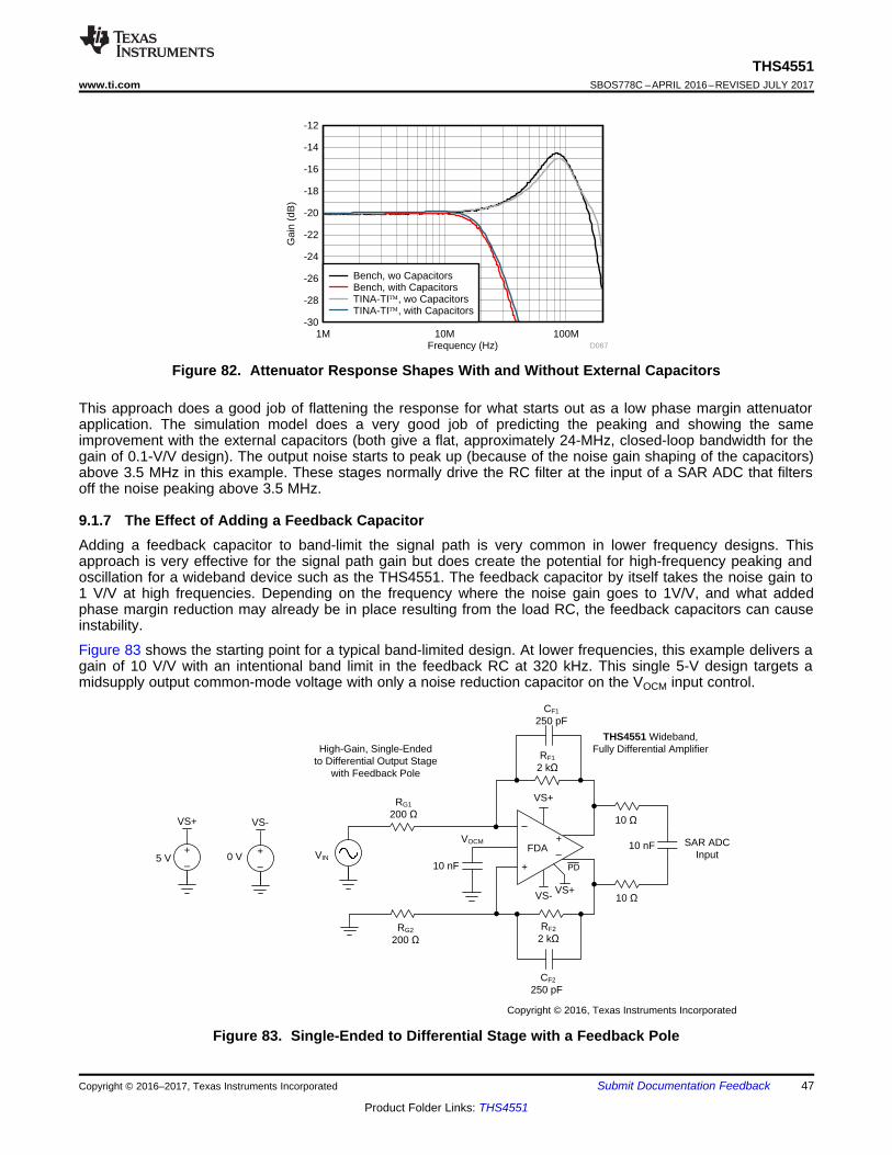
RF1
2 k
RG1
200
RG2
200
THS4551 Wideband,Fully Differential AmplifierHigh-Gain, Single-Ended
to Differential Output Stage with Feedback Pole
VOCM
RF2
2 k
+
±
VS+
+
±
VS+
FDA
PD
VS-
+
±
+
±5 V 0 V
CF1
250 pF
CF2
250 pF
VIN
VS+ VS-
10 nF
10
10
10 nF SAR ADCInput
Copyright © 2016, Texas Instruments Incorporated
Frequency (Hz)
Gai
n (d
B)
-30
-28
-26
-24
-22
-20
-18
-16
-14
-12
1M 10M 100MD067
Bench, wo CapacitorsBench, with CapacitorsTINA-TI�, wo CapacitorsTINA-TI�, with Capacitors
47
THS4551www.ti.com SBOS778C –APRIL 2016–REVISED JULY 2017
Product Folder Links: THS4551
Submit Documentation FeedbackCopyright © 2016–2017, Texas Instruments Incorporated
Figure 82. Attenuator Response Shapes With and Without External Capacitors
This approach does a good job of flattening the response for what starts out as a low phase margin attenuatorapplication. The simulation model does a very good job of predicting the peaking and showing the sameimprovement with the external capacitors (both give a flat, approximately 24-MHz, closed-loop bandwidth for thegain of 0.1-V/V design). The output noise starts to peak up (because of the noise gain shaping of the capacitors)above 3.5 MHz in this example. These stages normally drive the RC filter at the input of a SAR ADC that filtersoff the noise peaking above 3.5 MHz.
9.1.7 The Effect of Adding a Feedback CapacitorAdding a feedback capacitor to band-limit the signal path is very common in lower frequency designs. Thisapproach is very effective for the signal path gain but does create the potential for high-frequency peaking andoscillation for a wideband device such as the THS4551. The feedback capacitor by itself takes the noise gain to1 V/V at high frequencies. Depending on the frequency where the noise gain goes to 1V/V, and what addedphase margin reduction may already be in place resulting from the load RC, the feedback capacitors can causeinstability.
Figure 83 shows the starting point for a typical band-limited design. At lower frequencies, this example delivers again of 10 V/V with an intentional band limit in the feedback RC at 320 kHz. This single 5-V design targets amidsupply output common-mode voltage with only a noise reduction capacitor on the VOCM input control.
Figure 83. Single-Ended to Differential Stage with a Feedback Pole

RF1
2 k
RG1
200
RG2
200
THS4551 Wideband,Fully Differential AmplifierHigh-Gain, Single-Ended
to Differential Output Stage with Feedback Pole
VOCM
RF2
2 k
+
±
VS+
+
±
VS+
FDA
PD
VS-
+
±
+
±5 V 0 V
CF1
250 pF
CF2
250 pF
VIN
VS+ VS-
10 nF
10
10
10 nF SAR ADCInput
Copyright © 2016, Texas Instruments Incorporated
250 pF
Frequency (Hz)
Gai
n (d
B)
Pha
se (
deg)
-30 -50
-25 -25
-20 0
-15 25
-10 50
-5 75
0 100
5 125
10 150
15 175
20 200
100k 1M 10M 100M
D070
Gain (dB)Phase (deg)
48
THS4551SBOS778C –APRIL 2016–REVISED JULY 2017 www.ti.com
Product Folder Links: THS4551
Submit Documentation Feedback Copyright © 2016–2017, Texas Instruments Incorporated
The response shape must be probed at the FDA output pins before the added RC pole to the SAR input.Running a wideband sweep with the THS4551 TINA-TI™ model using the SBOC475 simulation file shows aresonance at 50 MHz in Figure 84 resulting from the feedback capacitor.
Figure 84. Gain and Phase Plot with a Feedback Pole
One approach to increasing the phase margin when there is a feedback capacitor is to include a differential inputcapacitor. This approach increases the noise gain at higher frequencies, thus creating a lower-frequency loopgain equal to a 0-dB crossover with more phase margin. Figure 85 shows a differential input capacitor equal tothe feedback capacitor in the test circuit. This approach increases the noise gain from 1 V/V at higherfrequencies (with only a feedback capacitor) to a noise gain of 3 V/V at higher frequencies.
Figure 85. Single-Ended to Differential Stage with a Feedback Pole and Differential Input Capacitor
Re-running the wideband response (using the SBOC474 TINA-TI™ simulation file) simulation illustrates inFigure 86 that the resonance is greatly reduced with the higher noise gain at the loop gain equal to a 0-dBcrossover at a lower frequency. Although this example is only modestly peaking, good design practice is toinclude a place for a differential input capacitor (even if not used) for any design using a feedback capacitoracross the feedback resistors. This recommendation applies to this simple example and to multiple feedbackactive filter designs.

RG1
1.57 k
RG2
1.57 k
THS4551 Wideband,Fully Differential Amplifier
VOCM
+
±
VS+
+
±
VS+
FDA
PD
VS-
100 fF
20
20
RF1
592
910 pF2.96 k
2.96 k 910 pFRF2
592
1.5 nF
OPA192 Output
+
±
+
±5 V 0 V
VS+ VS-
+
±2.048 V
VOCM
VIN
Copyright © 2016, Texas Instruments Incorporated
10
10
2.2 nF
100 pF
100 pF
8-VPP Differential SAR ADC Input
Frequency (Hz)
Gai
n (d
B)
Pha
se (
deg)
-60 -120
-50 -80
-40 -40
-30 0
-20 40
-10 80
0 120
10 160
20 200
100k 1M 10M 100M
D071
Gain (dB)Phase (deg)
49
THS4551www.ti.com SBOS778C –APRIL 2016–REVISED JULY 2017
Product Folder Links: THS4551
Submit Documentation FeedbackCopyright © 2016–2017, Texas Instruments Incorporated
Figure 86. Gain and Phase Plot with a Differential Input Capacitor
9.2 Typical Applications
9.2.1 An MFB Filter Driving an ADC ApplicationOne common application for the THS4551 is to take a single-ended, high VPP voltage swing (from a high-voltageprecision amplifier such as the OPA192) and deliver that swing to precision SAR ADC as a single-ended todifferential conversion with output common-mode control and implement an active 2nd-order multiple feedback(MFB) filter design. Designing for a 40-VPP maximum input down to an 8-VPP differential swing requires a gain of0.2 V/V. Targeting a 100-kHz Butterworth response with the RC elements tilted towards low noise gives theexample design of Figure 87. Note that the VCM control is set to half of a 4.096-V reference, which is typical for5-V differential SAR applications.
Figure 87. Example 100-kHz Butterworth Filter

T
Frequency (Hz)10k 100k 1MEG 10MEG 100MEG
Sig
nal t
o N
oise
[dB
]
110.00
120.00
130.00
140.00
150.00
Frequency (Hz)
Gai
n (d
B)
Pha
se (
deg)
-140 -600
-120 -450
-100 -300
-80 -150
-60 0
-40 150
-20 300
0 450
10k 100k 1M 10M 100M
D072
Gain (dB)Phase (deg)
50
THS4551SBOS778C –APRIL 2016–REVISED JULY 2017 www.ti.com
Product Folder Links: THS4551
Submit Documentation Feedback Copyright © 2016–2017, Texas Instruments Incorporated
Typical Applications (continued)9.2.1.1 Design RequirementsThe requirements for this application are:• Single-ended to differential conversion• Attenuation by 0.2-V/V gain• Active filter set to a Butterworth, 100-kHz response shape• Output RC elements set by SAR input requirements (not part of the filter design)• Filter element resistors and capacitors are set to limit added noise over the THS4551 and noise peaking
9.2.1.2 Detailed Design ProcedureThe design proceeds using the techniques and tools suggested in the Design Methodology for MFB Filters inADC Interface Applications application note (SBOA114). The process includes:• Scale the resistor values to not meaningfully contribute to the output noise produced by the THS4551 by itself• Select the RC ratios to hit the filter targets when reducing the noise gain peaking within the filter design• Set the output resistor to 10 Ω into a 2.2-nF differential capacitor• Add 100-pF common-mode capacitors to the load capacitor to improve common noise filtering• Inside the loop, add 20-Ω output resistors after the filter feedback capacitor to increase the isolation to the
load capacitor• Include a place for a differential input capacitor (illustrated as 100 fF in Figure 87)
9.2.1.3 Application CurvesProbing the response to the output pins by using the THS4551 SBOC471 TINA-TI™ simulation model (beforethe RC filter to the SAR ADC) illustrates the expected response plus some peaking at higher frequencies. Anysignal or noise peaking that appears at the output because of this peaking is rolled off by the RC filter betweenthe FDA and SAR inputs. A place for a differential input capacitor is illustrated in Figure 87 (as 0.1 pF) but is notused for this simulation. This slight peaking is a combination of low phase margin and feedthrough via thefeedback capacitor to the increasing open-loop output impedance of Figure 68. The loop gain and phaseresponse are available as a TINA-TI™ simulation file.
Obtaining the SNR to the ADC input pins, and assuming an 8-VPP full scale (2.83 VRMS), gives the result ofFigure 89. The 113-dB SNR shown in Figure 89 does not limit the performance for any SAR application.
Figure 88. Gain and Phase Plot for a 100-kHz ButterworthFilter Figure 89. Signal-to-Noise Ratio Plot

51
THS4551www.ti.com SBOS778C –APRIL 2016–REVISED JULY 2017
Product Folder Links: THS4551
Submit Documentation FeedbackCopyright © 2016–2017, Texas Instruments Incorporated
Typical Applications (continued)9.2.2 Differential Transimpedance Output to a High-Grade Audio PCM DAC ApplicationThe highest-grade audio digital-to-analog converters (DACs) are a differential current-mode output. Thesedevices normally suggest a two-amplifier transimpedance stage to hold the DAC output voltages fixed when theamplifiers produce a differential voltage swing at the outputs. Often, the differential voltage swing is thenconverted to single-ended in a differencing amplifier stage to drive headphone loads (see Figure 35 in theOPA1611). The emerging high-power class D audio amplifiers often require differential inputs. Applying theTHS4551 as a differential transimpedance stage offers a simple solution for very low-distortion, differential-outputaudio channels.
Starting with the output specifications for a very high-performance PCM1792A audio DAC, the requirements forthe THS4551 interface can be extracted. The DAC is a current-sourcing device that requires its outputs to beheld at ground when using a transimpedance amplifier. Using the DAC 3.3-V supply and the LM27762 low-noise,low-dropout (LDO) regulator and inverter provides a ±2.5-V supply to the THS4551. Operating the THS4551 on±2.5-V supplies places all nodes in range for an input VCM equal to GND (and the DAC output voltages as well)and an FDA output VOCM also equal to GND.
The center current in Table 6 is a fixed 6.2-mA dc current coming out of the DAC outputs regardless of the DACcode. This dc common-mode current can be absorbed by the –2.5-V supply at the input pins to hold the DACcompliance voltage and FDA input pins at ground. The FDA controls the output common-mode voltage, set toground in this case, whereas the input pin voltage (which does not move with the DAC output differential current)is controlled with a resistor to the negative supply.
Table 6. PCM1792A Analog Output SpecificationANALOG OUTPUT TEST CONDITION MIN TYP MAX UNIT
Gain error –6 ±2 6 % of FSRGain mismatch, channel-to-channel –3 ±0.5 3 % of FSRBipolar zero (BPZ) error At BPZ –2 ±0.5 2 % of FSROutput current Full-scale (0 dB) 7.8 mAPP
Center current At BPZ –6.2 mA
This bias is provided by the 402-Ω resistors to –2.5 V, as illustrated in Figure 90. This design takes thedifferential 7.8 mAPP from the DAC and produces a ±1.46-V swing on each output of the THS4551. Thisconfiguration gives a full-scale differential 5.85 VPP available on the ±2.5-V supply design centered at ground atboth the inputs and outputs. Although the LM27762 provides a very-low noise, –2.5-V supply, using 0.1%resistors in the current sink path to the –2.5-V supply as well as the feedback resistors limits any common-modenoise on the –2.5-V supply to differential mode conversion at the FDA outputs.

RF1
750
THS4551 Wideband,Fully Differential Amplifier
PCM1792AComplementary Current
Output DAC
VOCM
RF2
750
+
±
VS+
+
±
VS+
FDA
PD
VS-
+
±
+
±2.5 V -2.5 V
CF1
2.4 nF
CF2
2.4 nF
VS+ VS-
4.4
4.4
402
402
20 nF
VS-
VS-LM27762 Supplies
6.2 mA
6.2 mA
Copyright © 2016, Texas Instruments Incorporated
52
THS4551SBOS778C –APRIL 2016–REVISED JULY 2017 www.ti.com
Product Folder Links: THS4551
Submit Documentation Feedback Copyright © 2016–2017, Texas Instruments Incorporated
Figure 90. PCM1792A DAC Output Driver
9.2.2.1 Design RequirementsTo implement a differential transimpedance output interface to the PCM1792A DAC, the following requirementsmust be met:• The center current of the DAC must be considered to hold the DAC output voltage at ground. Using an FDA
controls the output side common-mode voltage, but the input common-mode voltage must also be controlledto ground.
• A direct means of sinking the center current is to add a pulldown resistor at the DAC outputs to a negativesupply. Generating a ±2.5-V supply for this current sink requirement and the THS4551 is accomplished withthe LM27762.
• The transimpedance gain can be set using the feedback resistors of the THS4551 FDA. These resistors arevery flexible, but when set, the bandwidth in this stage is set to 88 kHz using a feedback capacitor in parallelwith the resistive gain element.
• When the feedback capacitor is set, a differential input capacitor is added to increase the high-frequencynoise gain for the overall loop gain stability.
• These frequency response control capacitors interact with the inductive open-loop output impedance to forma high-frequency resonance. Adding a small series resistor to the feedback capacitor paths reduces thiseffect.
9.2.2.2 Detailed Design ProcedureProceed with this design using the techniques described in the Design for Wideband Differential TransimpedanceDAC Output application note (SBAA150):• Generate the bipolar balanced supplies using the LM27662.• Set the THS4551 output common-mode voltage at midsupply by grounding the VOCM pin.• Control the input pin operating voltage by sinking the center current out of the DAC to the –2.5-V supply with
precision 402-Ω resistors.• Set the gain for the complementary current output signal from the DAC by selecting the feedback resistor to
be 750 Ω. Set this resistor to keep the resulting output swing to be less than the available 9-VPP differentialswing.
• Control the bandwidth in this differential transimpedance stage to 88 kHz using the 2.4-nF feedback capacitoron each side.
• Increase the high-frequency noise gain to 17.7 V/V by adding a differential input capacitor of 20 nF.• Isolate these feedback capacitors with a series 4.4-Ω resistor in series with the feedback capacitors.

Time (ms)
Out
put V
olta
ge (
V)
0 0.2 0.4 0.6 0.8 1 1.2 1.4 1.6 1.8 2-2.5
-2
-1.5
-1
-0.5
0
0.5
1
1.5
2
2.5
D075
VOUT-VOUT+
Frequency (Hz)
Gai
n (d
B)
Pha
se (
deg)
20 -160
25 -120
30 -80
35 -40
40 0
45 40
50 80
55 120
60 160
65 200
70 240
1k 10k 100k 1M 10M 100M
D074
Gain (dB)Phase (deg)
53
THS4551www.ti.com SBOS778C –APRIL 2016–REVISED JULY 2017
Product Folder Links: THS4551
Submit Documentation FeedbackCopyright © 2016–2017, Texas Instruments Incorporated
9.2.2.3 Application CurvesThe bandwidth is controlled to 88 kHz by using the 2.4-nF feedback capacitors. Amplifier stability is controlled bythe 20-nF differential capacitor across the DAC outputs. The added 4.4 Ω in series with the feedback 2.2-nFcapacitor isolates this capacitance from the inductive open-loop output impedance. To observe the effect ofadding these small resistors in series with the feedback capacitors, use the TINA-TI™ loop gain simulationcircuit. Include the DAC source capacitance in any final design analysis. Running the frequency response for thiscircuit (available as a TINA-TI™ simulation file) provides this result. The 63.5-dBΩ gain is the 1.5-kΩtransimpedance gain provided in this design.
Figure 91. Gain and Phase Plot of DAC Output Driver
Running a full-scale sine wave at 1 kHz with ±1.95 mA on each output from the DAC at 180° out of phase, andprobing each THS4551 output pin separately results in the expected ±1.46 V on each output pin, as shown inFigure 92. More output swing is available for the RRO device using the ±2.5-V supplies provided by theLM27762 by simply increasing the feedback resistor values.
Figure 92. Output Waveform of the DAC Output Driver
Although this example is on the audio signal generation side, the THS4551 can also be used to convert a single-ended line input to a differential driver into an audio ADC.

RF1
1 k
RG1
187
RG2
215
RT1
59
THS4551 Wideband,Fully Differential Amplifier
50- �Input Match, Gain of 5 V/V from RT, Single-Ended Source to
Differential Output
VOCM
RF2
1 k
+
±
VS+
+
±
VS+
FDA
PD
VS-
50- �Source Impedance
40.2
40.2
732 ADC3241
Inputs
VOUT
10-MHz,Second-OrderBessel Filter
VIN
RS1
50
360 pF
5.6
5.6
+
±
+
±3.3 V 0 V
VS+ VS-
+
±950 mV
VOCM
390 nH
390 nH
Copyright © 2016, Texas Instruments Incorporated
ADC OutputCommon-Mode
Voltage
54
THS4551SBOS778C –APRIL 2016–REVISED JULY 2017 www.ti.com
Product Folder Links: THS4551
Submit Documentation Feedback Copyright © 2016–2017, Texas Instruments Incorporated
9.2.3 ADC3k Driver with a 2nd-Order RLC Interstage Filter ApplicationThe THS4551 is well suited to low-power, dc-coupled requirements driving low-power pipeline ADCs (such asthe ADC3241 25-MSPS, 14-bit, dual device). Figure 93 shows an example design taking a bipolar input to a–1-dBFS swing at the ADC input of 1.8 VPP. In this case, a 50-Ω source and input matching is assumed with again of 5 V/V to the output pins with a 2nd-order interstage filter adding a –1-dB insertion loss. Full-scale voltageat the input of RT and RG1 is then ±0.2 V. The 0.95-V output common-mode voltage is provided by the ADC. Theoutput filter provides a noise-power bandwidth limit with a low overshoot step response with no common-modelevel shift from the 0.95-V voltage provided by the ADC.
Figure 93. ADC3k Driver with a 2nd-Order RLC Interstage Filter
9.2.3.1 Design RequirementsFor this design example, the requirements include:• Provide a wideband, 50-Ω input impedance match for a single-ended source centered on ground.• From the input termination, provide a gain of 5 V/V to the FDA output pins as a differential signal.• Set the output common-mode operating point using the ADC common-mode output voltage as the VOCM
input to the THS4551 FDA.• Implement a low-overshoot, noise-band-limiting filter between the FDA and the ADC. Use only differential
shunt elements in the filter to pass the FDA output common-mode voltage to the ADC with no level shifting.• Design the filter as a –1-dB insertion loss filter with a low series resistor to limit the common-mode level shift
resulting from the ADC input sample-rate-dependent common-mode current.
9.2.3.2 Detailed Design ProcedureThe design proceeds as follows:• Select the feedback resistor to be 1 kΩ and use the values from Table 2 at a gain of 5 V/V to implement a
50-Ω input match with a gain of 5 V/V.• Use a 3.3-V power supply and apply the ADC output common-mode voltage to the VOCM input pin of the
THS4551.• Design a –1-dB insertion loss, 2nd-order RLC filter using the approach described in the RLC Filter Design for
ADC Interface Applications application note (SBAA108).• Adjust the total resistive load target in the filter design to hit the standard value for the filter inductors.• Convert the filter design to differential with only differential shunt elements. These elements must not be split
and connected to a center-point ground. This technique passes the output common-mode voltage from theFDA to the ADC with no level shift error.
• Add a small series resistor at the ADC inputs. This resistor is not part of the filter design but spreads out thesampling glitch energy to provide improved SFDR.
• Check the common-mode level shift from the FDA outputs to the ADC resulting from the clock-rate-dependentcommon-mode current. This common-mode current into the ADC shifts the common-mode voltage slightly,but can easily stay in range with a low series resistor in the filter design.

Time (ns)
Vol
tage
(V
)
0 100 200 300 400 500 600 700 800 900 1000-1.5
-1
-0.5
0
0.5
1
1.5
D076
VIN+VOUTVIN
55
THS4551www.ti.com SBOS778C –APRIL 2016–REVISED JULY 2017
Product Folder Links: THS4551
Submit Documentation FeedbackCopyright © 2016–2017, Texas Instruments Incorporated
9.2.3.3 Application CurveDriving a 2-MHz ±0.2-V square wave into this circuit (using a TINA-TI™ simulation file for the circuit of Figure 93)gives the response shown in Figure 94 at the ADC. The red trace is a –1-dBFS, 1.8-VPP square wave at the ADCinput pins. The gray trace is the input signal at the RT termination resistor. The black trace is the common-modevoltage at the FDA input pins. Note that the input pin voltage swing stays above ground and in range for thisbipolar input, single, 3.3-V supply design.
Figure 94. Time-Domain Waveform
Unbuffered pipeline ADCs draw a clock-rate-dependent input common-mode current. For the ADC3241, thisinput current is specified as 1.5 µA per MSPS. Operating at 25 MSPS, the common-mode current drops thecommon-mode voltage from 0.95 V at the THS4551 outputs by 37.5 µA × 45.8 Ω = 1.7 mV to 0.9483 V. Thisvalue is well within the allowed ±25-mV common-mode deviation from the ADC VCM output. Consider this effectcarefully when using higher resistor values in the interface at the ADC.

Junction Temperature (qC)
Sup
ply
Cur
rent
(m
A)
-45 -30 -15 0 15 30 45 60 75 90 105 120 1351
1.1
1.2
1.3
1.4
1.5
1.6
1.7
1.8
D068
56
THS4551SBOS778C –APRIL 2016–REVISED JULY 2017 www.ti.com
Product Folder Links: THS4551
Submit Documentation Feedback Copyright © 2016–2017, Texas Instruments Incorporated
10 Power Supply RecommendationsThe THS4551 is principally intended to operate with a nominal single-supply voltage of 3 V to 5 V. Supplyvoltage tolerances are supported with the specified operating range of 2.7 V (10% low on a 3-V nominal supply)and 5.4 V (8% high on a 5-V nominal supply). Supply decoupling is required, as described in the Terminologyand Application Assumptions section. Split (or bipolar) supplies can be used with the THS4551, as long as thetotal value across the device remains less than 5.5 V (absolute maximum). The thermal pad on the RGTpackage is electrically isolated form the die; connect the thermal pad (RGT package only) to any power orground plane for reduced thermal impedance to the junction temperature. This pad must be connected to somepower or ground plane and not floated.
For the best input offset voltage drift, the THS4551 uses a proportional to absolute temperature (PTAT)quiescent current biasing scheme. This approach gives a positive over temperature variation in supply current.Figure 95 shows the 5-V supply current over a wide TJ range for a number of tested units. The ElectricalCharacteristics tables report the typical and range on this supply current temperature coefficient for both 5-V and3-V supply operation.
Figure 95. Linear Temperature Coefficient for Supply Current
Using a negative supply to deliver a true swing to ground output when driving SAR ADCs can be desired.Although the THS4551 quotes a rail-to-rail output, linear operation requires approximately 200-mV headroom tothe supply rails. One easy option for extending the linear output swing to ground is to provide the small negativesupply voltage required using the LM7705 fixed –230-mV, negative-supply generator. This low-cost, fixed,negative-supply generator can accept the 3-V to 5-V positive supply input used by the THS4551 and provides afixed –230-mV supply for the negative power supply. Using the LM7705 provides an effective solution, asdiscussed in the Extending Rail-to-Rail Output Range for Fully Differential Amplifiers to Include True Zero VoltsTI design (TIDU187)

57
THS4551www.ti.com SBOS778C –APRIL 2016–REVISED JULY 2017
Product Folder Links: THS4551
Submit Documentation FeedbackCopyright © 2016–2017, Texas Instruments Incorporated
10.1 Thermal AnalysisThe very low internal quiescent power dissipation for the THS4551, combined with the excellent thermalimpedance of the 16-pin VQFN package (RGT), limits the possibility of excessively high internal junctiontemperatures. A more detailed analysis may be warranted because the 10-pin WQFN (RUN) package has amuch higher junction-to-ambient thermal impedance (θJA = 163°C/W).
To estimate the internal TJ, an estimate of the maximum internal power dissipation is first required. There are twopieces to the internal power dissipation: quiescent current power and the power used in the output stage todeliver load current. To simplify the latter, the worst-case output stage power drives a dc differential voltageacross a load using half the total supply voltage. Also assume a maximum ambient temperature of 125°C, givingthe maximum quiescent current as shown in Figure 95. As an example:• Assume a maximum operating supply voltage of 5.4 V. This 5.4-V supply with a maximum ICC of 1.75 mA
gives a quiescent power term of 9.45 mW.• Assume a 200-Ω differential load with a static 2.7-V differential voltage established across the load. The
1.35 mA of dc load current generates a maximum output stage power of (5.4 V – 2.7 V) × 1.35 mA =3.65 mW.
• From the worst-case total internal PD of 13.1 mW, multiplying the internal PD with a 163°C/W thermalimpedance times the 163°C/W thermal impedance for the very small 10-pin WQFN package results in a 2.1°Crise from ambient.
Even for this extreme condition and the maximum-rated ambient of 125°C, the junction temperature is amaximum of 127°C, which is less than the rated absolute maximum of 150°C. Follow this same calculationsequence for the exact application and package selected to predict the maximum TJ.
11 Layout
11.1 Layout Guidelines
11.1.1 Board Layout RecommendationsSimilar to all high-speed devices, best system performance is achieved with close attention to board layout. TheTHS4551DGKEVM user guide (SLOU447) shows a good example of high-frequency layout techniques as areference. This EVM includes numerous extra elements and features for characterization purposes that may notapply to some applications. General high-speed signal path layout suggestions include:• Continuous ground planes are preferred for signal routing with matched impedance traces for longer runs;
however, both ground and power planes must be opened up around the capacitive sensitive input and outputdevice pins. When the signal goes to a resistor, parasitic capacitance becomes more of a band-limiting issueand less of a stability issue.
• Good high-frequency decoupling capacitors (0.1 µF) are required to a ground plane at the device power pins.Additional higher-value capacitors (2.2 µF) are also required but can be placed further from the device powerpins and shared among devices. For best high-frequency decoupling, consider X2Y supply decouplingcapacitors that offer a much higher self-resonance frequency over standard capacitors.
• Differential signal routing over any appreciable distance must use microstrip layout techniques with matchedimpedance traces.
• Higher-speed FDAs such as the THS4551 include a duplicate of the output pins on the input feedback side ofthe larger 16-pin VQFN (RGT) package. This feature is intended to allow the external feedback resistors to beconnected with virtually no trace length on the input side of the package. This internal feedback trace alsoprovides a second feedback path for connecting a feedback capacitor on the input pin sides for band-limitedor multiple feedback filter designs. This internal trace shows an approximate 3.3-Ω series resistance that mustbe considered in any design using that path. The TINA-TI™ model does not include that element (to begenerally applicable to all package styles) and must be added externally if the RGT package is used. Use thislayout approach without extra trace length on the critical feedback path. The smaller 10-pin WQFN packagelines up the outputs and the required inputs on the same side of the package where the feedback RF resistorsmust be placed immediately adjacent to the package with minimal trace length.
• The input summing junctions are very sensitive to parasitic capacitance. Any RG elements must connect intothe summing junction with minimal trace length to the device pin side of the resistor. The other side of the RGelements can have more trace length if needed to the source or to GND.

58
THS4551SBOS778C –APRIL 2016–REVISED JULY 2017 www.ti.com
Product Folder Links: THS4551
Submit Documentation Feedback Copyright © 2016–2017, Texas Instruments Incorporated
11.2 Layout Example
Figure 96. Example Layout

59
THS4551www.ti.com SBOS778C –APRIL 2016–REVISED JULY 2017
Product Folder Links: THS4551
Submit Documentation FeedbackCopyright © 2016–2017, Texas Instruments Incorporated
11.3 EVM BoardFigure 97 and Figure 98 show the layout of the top and bottom layers of the THS4551DGKEVM evaluationmodule, respectively.
Figure 97. THS4551DGKEVM Top Layer
Figure 98. THS4551DGKEVM Bottom Layer

60
THS4551SBOS778C –APRIL 2016–REVISED JULY 2017 www.ti.com
Product Folder Links: THS4551
Submit Documentation Feedback Copyright © 2016–2017, Texas Instruments Incorporated
12 Device and Documentation Support
12.1 Device Support
12.1.1 TINA-TI™ Simulation Model FeaturesThe device model is available on the product folder under www.ti.com in a typical application circuit file. Themodel includes numerous features intended to speed designer progress over a wide range of applicationrequirements. The following list shows the performance parameters included in the model:• For the small-signal response shape with any external circuit:
– Differential open-loop gain and phase– Parasitic input capacitance– Open-loop differential output impedance
• For noise simulations:– Input differential spot voltage noise and a 100-Hz 1/f corner– Input current noise on each input with a 6-kHz 1/f corner
• For time-domain, step-response simulations:– Differential slew rate– I/O headroom models to predict clipping– Input stage diodes to predict overdrive limiting
• Fine-scale, dc precision terms:– PSRR– CMRR
The Typical Characteristics: 3-V to 5-V Supply Range section provides more detail than the macromodels canprovide; some of the unmodeled features include:• Harmonic distortion• Temperature drift in dc error terms (VIO and IOS)• Overdrive recovery time• Turn-on and turn-off times using the power-down feature
Some unique simulation considerations come with the THS4551 TINA-TI™ model. This device (and model)include 0.6-pF internal feedback capacitors. These capacitors are intended to improve phase margin when usinghigher external feedback resistor values. Higher feedback resistors generate an in-band pole in the feedbacksignal with the differential input capacitance, and the internal 0.6 pF capacitors add a zero to the feedbackresponse shape to shape the noise gain flat at the loop-gain crossover.
In order to generate an accurate open-loop gain and phase simulation, these components must be removedbecause they are feedback elements, not forward path elements. Figure 99 illustrates a typical AOL gain andphase simulation (available as a TINA-TI™ software file) where external –0.6-pF capacitors cancel out theinternal capacitors in the model (TINA-TI™ supports negative value elements). The inductors inside the loopclose the loop for the dc operating point and open the loop immediately for an ac sweep. The input-couplingcapacitors are open at dc, then couple in the differential input immediately on an ac sweep. The somewhat oddvalues help reduce numerical chatter in the simulation. When using the internal feedback traces from the outputsto the inputs on the RGT package, be sure to add the 3.3-Ω trace impedance to any simulation. This impedanceis not included in the core model.

T
Ga
in (
dB
)
-100.00
0.00
100.00
200.00
Frequency (Hz)
10.00 100.00 1.00k 10.00k 100.00k 1.00MEG 10.00MEG 100.00MEG 1.00G
Ph
ase
[de
g]
-400.00
-300.00
-200.00
-100.00
0.00
VOCM
VS
+V
S±
VS
+
VS
+
VS±
VO
CM
VIN+
VIN-
VIN-
VIN+ R3
100
k:
R1 10 m:
R2 10 m:
V1 2.5 V2 -2.5V4 0
-
+
++
-
VOCM
-
U1 THS4551
+
VG1-
+
-
+
VCVS1 1R410 M:
R510 M:
V
+
VM1
C1 -600 fF
C2 -600 fF
L1 9
99 H
L2 9
99 H
C3 9.97 kF
C4 9.97 kF
Copyright © 2016, Texas Instruments Incorporated
61
THS4551www.ti.com SBOS778C –APRIL 2016–REVISED JULY 2017
Product Folder Links: THS4551
Submit Documentation FeedbackCopyright © 2016–2017, Texas Instruments Incorporated
Device Support (continued)
Figure 99. Open-Loop Gain and Phase TINA-TI™ Simulation Setup
This test is set up with a very light load to isolate the no load AOL curve. Adding a load brings in the open-loopZOL response to the overall response of the output pins. Running this simulation gives the gain and phase ofFigure 100 that closely matches the plot of Figure 37.
Figure 100. Open-Loop Gain and Phase Simulation Result

62
THS4551SBOS778C –APRIL 2016–REVISED JULY 2017 www.ti.com
Product Folder Links: THS4551
Submit Documentation Feedback Copyright © 2016–2017, Texas Instruments Incorporated
12.2 Documentation Support
12.2.1 Related DocumentationFor related documentation see the following:• THS4551 TINA-TI™ model• THS4551DGKEVM User Guide (SLOU447)• THS452x Very Low Power, Negative Rail Input, Rail-To-Rail Output, Fully Differential Amplifier (SBOS458)• LMH6629 Ultra-Low Noise, High-Speed Operational Amplifier with Shutdown (SNOSB18)• OPA847 Wideband, Ultra-Low Noise, Voltage-Feedback Operational Amplifier with Shutdown (SBOS251)• INA188 Precision, Zero-Drift, Rail-to-Rail Out, High-Voltage Instrumentation Amplifier (SBOS632)• OPAx192 36-V, Precision, Rail-to-Rail Input/Output, Low Offset Voltage, Low Input Bias Current Op Amp with
e-trim™ (SBOS620)• OPA161x SoundPlus™ High-Performance, Bipolar-Input Audio Operational Amplifiers (SBOS450)• ADC322x Dual-Channel, 12-Bit, 25-MSPS to 125-MSPS, Analog-to-Digital Converters (SBAS672)• ADC324x Dual-Channel, 14-Bit, 25-MSPS to 125-MSPS, Analog-to-Digital Converters (SBAS671)• ADS127L01 24-Bit, High-Speed, Wide-Bandwidth Analog-to-Digital Converter (SBAS607)• ADS127L01EVM User's Guide (SBAU261)• ADS9110 18-Bit, 2-MSPS, 15-mW, SAR ADC with multiSPI™ Interface (SBAS629)• REF6025EVM-PDK User's Guide (SBAU258)• 24-Bit, 192-kHz Sampling, Advanced Segment, Audio Stereo Digital-to-Analog Converter (SLES105)• LM27762 Low-Noise Regulated Switched-Capacitor Voltage Inverter (SNVSAF7)• LM7705 Low-Noise Negative Bias Generator (SNVS420)• Extending Rail-to-Rail Output Range for Fully Differential Amplifiers to Include True Zero Volts (TIDU187)• Design Methodology for MFB Filters in ADC Interface Applications (SBOA114)• Design for Wideband Differential Transimpedance DAC Output (SBAA150)• RLC Filter Design for ADC Interface Applications (SBAA108)• TINA-TI Open Loop No Load Response (SBOC476)• TINA-TI Basic Gain of 1 Test Circuit (SBOC466)• TINA-TI ADTL1-4-75 Model Test (SBOC463)• TINA-TI Common Mode Test CKT (SBOC467)• TINA-TI AC Coupled Single to Differentiate Gain of 2 (SBOC460)• TINA-TI Single to Differential Attenuator (SBOC477)• TINA-TI Gain of 5 Single to Different Simplified (SBOC472)• TINA-TI AC coupled different IO (SLOC341)• TINA-TI Differential IO with OPA2192 to FDA to SAR (SBOC469)• TINA-TI ADS127L01 MFB Driver (SBOC462)• TINA-TI ADS127L01 MFB Driver LG Test (SBOC461)• TINA-TI Attenuator With No Caps Gain of 0.1 (SBOC465)• TINA-TI Attenuator With a Caps Gain of 0.1 (SBOC464)• TINA-TI High Gain Single to Different with Feedback Pole (SBOC475)• TINA-TI High Gain Single to Different with Feedback Pole and Input C (SBOC474)• TINA-TI Gain of 0.2 100kHz Butterworth MFB Filter (SBOC471)• TINA-TI 100kHz MFB filter LG test (SBOC459)• TINA-TI Differential Transimpedance LG Sim (SBOC470)• TINA-TI Differential Audio DAC ZT Design (SBOC468)• TINA-TI Gain of 5 Single to Different with 10Mhz Bessel (SBOC473)
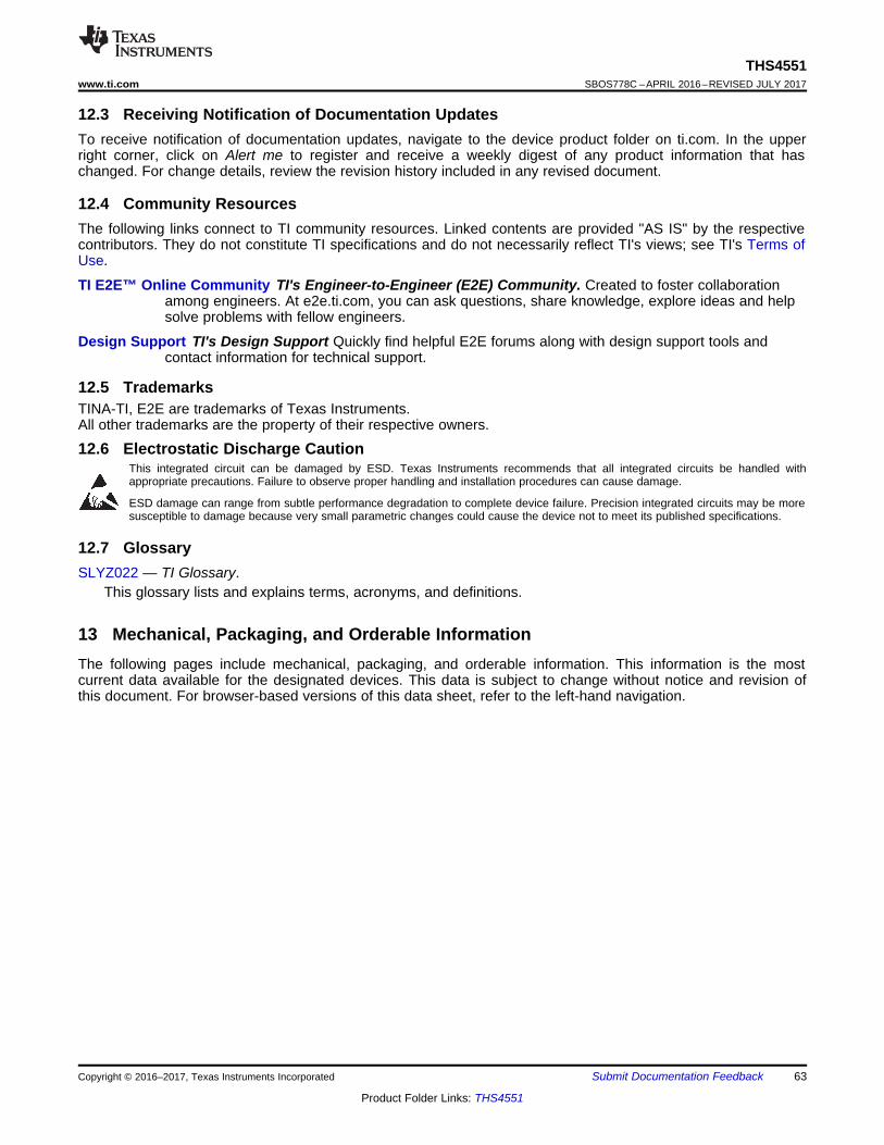
63
THS4551www.ti.com SBOS778C –APRIL 2016–REVISED JULY 2017
Product Folder Links: THS4551
Submit Documentation FeedbackCopyright © 2016–2017, Texas Instruments Incorporated
12.3 Receiving Notification of Documentation UpdatesTo receive notification of documentation updates, navigate to the device product folder on ti.com. In the upperright corner, click on Alert me to register and receive a weekly digest of any product information that haschanged. For change details, review the revision history included in any revised document.
12.4 Community ResourcesThe following links connect to TI community resources. Linked contents are provided "AS IS" by the respectivecontributors. They do not constitute TI specifications and do not necessarily reflect TI's views; see TI's Terms ofUse.
TI E2E™ Online Community TI's Engineer-to-Engineer (E2E) Community. Created to foster collaborationamong engineers. At e2e.ti.com, you can ask questions, share knowledge, explore ideas and helpsolve problems with fellow engineers.
Design Support TI's Design Support Quickly find helpful E2E forums along with design support tools andcontact information for technical support.
12.5 TrademarksTINA-TI, E2E are trademarks of Texas Instruments.All other trademarks are the property of their respective owners.
12.6 Electrostatic Discharge CautionThis integrated circuit can be damaged by ESD. Texas Instruments recommends that all integrated circuits be handled withappropriate precautions. Failure to observe proper handling and installation procedures can cause damage.
ESD damage can range from subtle performance degradation to complete device failure. Precision integrated circuits may be moresusceptible to damage because very small parametric changes could cause the device not to meet its published specifications.
12.7 GlossarySLYZ022 — TI Glossary.
This glossary lists and explains terms, acronyms, and definitions.
13 Mechanical, Packaging, and Orderable InformationThe following pages include mechanical, packaging, and orderable information. This information is the mostcurrent data available for the designated devices. This data is subject to change without notice and revision ofthis document. For browser-based versions of this data sheet, refer to the left-hand navigation.

PACKAGE OPTION ADDENDUM
www.ti.com 11-Aug-2017
Addendum-Page 1
PACKAGING INFORMATION
Orderable Device Status(1)
Package Type PackageDrawing
Pins PackageQty
Eco Plan(2)
Lead/Ball Finish(6)
MSL Peak Temp(3)
Op Temp (°C) Device Marking(4/5)
Samples
THS4551IDGKR ACTIVE VSSOP DGK 8 2500 Green (RoHS& no Sb/Br)
CU NIPDAUAG Level-2-260C-1 YEAR -40 to 125 4551
THS4551IDGKT ACTIVE VSSOP DGK 8 250 Green (RoHS& no Sb/Br)
CU NIPDAUAG Level-2-260C-1 YEAR -40 to 125 4551
THS4551IRGTR ACTIVE VQFN RGT 16 3000 Green (RoHS& no Sb/Br)
CU NIPDAU Level-2-260C-1 YEAR -40 to 125 HS4551
THS4551IRGTT ACTIVE VQFN RGT 16 250 Green (RoHS& no Sb/Br)
CU NIPDAU Level-2-260C-1 YEAR -40 to 125 HS4551
THS4551IRUNR ACTIVE QFN RUN 10 3000 Green (RoHS& no Sb/Br)
CU NIPDAU Level-2-260C-1 YEAR -40 to 125 4551
THS4551IRUNT ACTIVE QFN RUN 10 250 Green (RoHS& no Sb/Br)
CU NIPDAU Level-2-260C-1 YEAR -40 to 125 4551
(1) The marketing status values are defined as follows:ACTIVE: Product device recommended for new designs.LIFEBUY: TI has announced that the device will be discontinued, and a lifetime-buy period is in effect.NRND: Not recommended for new designs. Device is in production to support existing customers, but TI does not recommend using this part in a new design.PREVIEW: Device has been announced but is not in production. Samples may or may not be available.OBSOLETE: TI has discontinued the production of the device.
(2) RoHS: TI defines "RoHS" to mean semiconductor products that are compliant with the current EU RoHS requirements for all 10 RoHS substances, including the requirement that RoHS substancedo not exceed 0.1% by weight in homogeneous materials. Where designed to be soldered at high temperatures, "RoHS" products are suitable for use in specified lead-free processes. TI mayreference these types of products as "Pb-Free".RoHS Exempt: TI defines "RoHS Exempt" to mean products that contain lead but are compliant with EU RoHS pursuant to a specific EU RoHS exemption.Green: TI defines "Green" to mean the content of Chlorine (Cl) and Bromine (Br) based flame retardants meet JS709B low halogen requirements of <=1000ppm threshold. Antimony trioxide basedflame retardants must also meet the <=1000ppm threshold requirement.
(3) MSL, Peak Temp. - The Moisture Sensitivity Level rating according to the JEDEC industry standard classifications, and peak solder temperature.
(4) There may be additional marking, which relates to the logo, the lot trace code information, or the environmental category on the device.
(5) Multiple Device Markings will be inside parentheses. Only one Device Marking contained in parentheses and separated by a "~" will appear on a device. If a line is indented then it is a continuationof the previous line and the two combined represent the entire Device Marking for that device.

PACKAGE OPTION ADDENDUM
www.ti.com 11-Aug-2017
Addendum-Page 2
(6) Lead/Ball Finish - Orderable Devices may have multiple material finish options. Finish options are separated by a vertical ruled line. Lead/Ball Finish values may wrap to two lines if the finishvalue exceeds the maximum column width.
Important Information and Disclaimer:The information provided on this page represents TI's knowledge and belief as of the date that it is provided. TI bases its knowledge and belief on informationprovided by third parties, and makes no representation or warranty as to the accuracy of such information. Efforts are underway to better integrate information from third parties. TI has taken andcontinues to take reasonable steps to provide representative and accurate information but may not have conducted destructive testing or chemical analysis on incoming materials and chemicals.TI and TI suppliers consider certain information to be proprietary, and thus CAS numbers and other limited information may not be available for release.
In no event shall TI's liability arising out of such information exceed the total purchase price of the TI part(s) at issue in this document sold by TI to Customer on an annual basis.

TAPE AND REEL INFORMATION
*All dimensions are nominal
Device PackageType
PackageDrawing
Pins SPQ ReelDiameter
(mm)
ReelWidth
W1 (mm)
A0(mm)
B0(mm)
K0(mm)
P1(mm)
W(mm)
Pin1Quadrant
THS4551IDGKR VSSOP DGK 8 2500 330.0 12.4 5.3 3.4 1.4 8.0 12.0 Q1
THS4551IDGKT VSSOP DGK 8 250 330.0 12.4 5.3 3.4 1.4 8.0 12.0 Q1
THS4551IRGTR VQFN RGT 16 3000 330.0 12.4 3.3 3.3 1.1 8.0 12.0 Q2
THS4551IRGTT VQFN RGT 16 250 180.0 12.4 3.3 3.3 1.1 8.0 12.0 Q2
PACKAGE MATERIALS INFORMATION
www.ti.com 30-Apr-2018
Pack Materials-Page 1

*All dimensions are nominal
Device Package Type Package Drawing Pins SPQ Length (mm) Width (mm) Height (mm)
THS4551IDGKR VSSOP DGK 8 2500 366.0 364.0 50.0
THS4551IDGKT VSSOP DGK 8 250 366.0 364.0 50.0
THS4551IRGTR VQFN RGT 16 3000 367.0 367.0 35.0
THS4551IRGTT VQFN RGT 16 250 210.0 185.0 35.0
PACKAGE MATERIALS INFORMATION
www.ti.com 30-Apr-2018
Pack Materials-Page 2


www.ti.com
PACKAGE OUTLINE
C
16X 0.300.18
1.68 0.07
16X 0.50.3
1 MAX
(0.2) TYP
0.050.00
12X 0.5
4X1.5
A 3.12.9
B
3.12.9
VQFN - 1 mm max heightRGT0016CPLASTIC QUAD FLATPACK - NO LEAD
4222419/B 11/2016
PIN 1 INDEX AREA
0.08
SEATING PLANE
1
49
12
5 8
16 13
(OPTIONAL)PIN 1 ID 0.1 C A B
0.05
EXPOSEDTHERMAL PAD
SYMM
SYMM
NOTES: 1. All linear dimensions are in millimeters. Any dimensions in parenthesis are for reference only. Dimensioning and tolerancing per ASME Y14.5M. 2. This drawing is subject to change without notice. 3. The package thermal pad must be soldered to the printed circuit board for thermal and mechanical performance.
SCALE 3.600

www.ti.com
EXAMPLE BOARD LAYOUT
0.07 MINALL AROUND
0.07 MAXALL AROUND
16X (0.24)
16X (0.6)
( 0.2) TYPVIA
12X (0.5)
(2.8)
(2.8)
(0.58)TYP
( 1.68)
(R0.05)ALL PAD CORNERS
(0.58) TYP
VQFN - 1 mm max heightRGT0016CPLASTIC QUAD FLATPACK - NO LEAD
4222419/B 11/2016
SYMM
1
4
5 8
9
12
1316
SYMM
LAND PATTERN EXAMPLESCALE:20X
NOTES: (continued) 4. This package is designed to be soldered to a thermal pad on the board. For more information, see Texas Instruments literature number SLUA271 (www.ti.com/lit/slua271).5. Vias are optional depending on application, refer to device data sheet. If any vias are implemented, refer to their locations shown on this view. It is recommended that vias under paste be filled, plugged or tented.
SOLDER MASKOPENING
METAL UNDERSOLDER MASK
SOLDER MASKDEFINED
METAL
SOLDER MASKOPENING
SOLDER MASK DETAILS
NON SOLDER MASKDEFINED
(PREFERRED)

www.ti.com
EXAMPLE STENCIL DESIGN
16X (0.6)
16X (0.24)
12X (0.5)
(2.8)
(2.8)
( 1.55)
(R0.05) TYP
VQFN - 1 mm max heightRGT0016CPLASTIC QUAD FLATPACK - NO LEAD
4222419/B 11/2016
NOTES: (continued) 6. Laser cutting apertures with trapezoidal walls and rounded corners may offer better paste release. IPC-7525 may have alternate design recommendations.
SYMM
ALL AROUNDMETAL
SOLDER PASTE EXAMPLEBASED ON 0.125 mm THICK STENCIL
EXPOSED PAD 17:
85% PRINTED SOLDER COVERAGE BY AREA UNDER PACKAGESCALE:25X
SYMM
1
4
5 8
9
12
1316
17

IMPORTANT NOTICE
Texas Instruments Incorporated (TI) reserves the right to make corrections, enhancements, improvements and other changes to itssemiconductor products and services per JESD46, latest issue, and to discontinue any product or service per JESD48, latest issue. Buyersshould obtain the latest relevant information before placing orders and should verify that such information is current and complete.TI’s published terms of sale for semiconductor products (http://www.ti.com/sc/docs/stdterms.htm) apply to the sale of packaged integratedcircuit products that TI has qualified and released to market. Additional terms may apply to the use or sale of other types of TI products andservices.Reproduction of significant portions of TI information in TI data sheets is permissible only if reproduction is without alteration and isaccompanied by all associated warranties, conditions, limitations, and notices. TI is not responsible or liable for such reproduceddocumentation. Information of third parties may be subject to additional restrictions. Resale of TI products or services with statementsdifferent from or beyond the parameters stated by TI for that product or service voids all express and any implied warranties for theassociated TI product or service and is an unfair and deceptive business practice. TI is not responsible or liable for any such statements.Buyers and others who are developing systems that incorporate TI products (collectively, “Designers”) understand and agree that Designersremain responsible for using their independent analysis, evaluation and judgment in designing their applications and that Designers havefull and exclusive responsibility to assure the safety of Designers' applications and compliance of their applications (and of all TI productsused in or for Designers’ applications) with all applicable regulations, laws and other applicable requirements. Designer represents that, withrespect to their applications, Designer has all the necessary expertise to create and implement safeguards that (1) anticipate dangerousconsequences of failures, (2) monitor failures and their consequences, and (3) lessen the likelihood of failures that might cause harm andtake appropriate actions. Designer agrees that prior to using or distributing any applications that include TI products, Designer willthoroughly test such applications and the functionality of such TI products as used in such applications.TI’s provision of technical, application or other design advice, quality characterization, reliability data or other services or information,including, but not limited to, reference designs and materials relating to evaluation modules, (collectively, “TI Resources”) are intended toassist designers who are developing applications that incorporate TI products; by downloading, accessing or using TI Resources in anyway, Designer (individually or, if Designer is acting on behalf of a company, Designer’s company) agrees to use any particular TI Resourcesolely for this purpose and subject to the terms of this Notice.TI’s provision of TI Resources does not expand or otherwise alter TI’s applicable published warranties or warranty disclaimers for TIproducts, and no additional obligations or liabilities arise from TI providing such TI Resources. TI reserves the right to make corrections,enhancements, improvements and other changes to its TI Resources. TI has not conducted any testing other than that specificallydescribed in the published documentation for a particular TI Resource.Designer is authorized to use, copy and modify any individual TI Resource only in connection with the development of applications thatinclude the TI product(s) identified in such TI Resource. NO OTHER LICENSE, EXPRESS OR IMPLIED, BY ESTOPPEL OR OTHERWISETO ANY OTHER TI INTELLECTUAL PROPERTY RIGHT, AND NO LICENSE TO ANY TECHNOLOGY OR INTELLECTUAL PROPERTYRIGHT OF TI OR ANY THIRD PARTY IS GRANTED HEREIN, including but not limited to any patent right, copyright, mask work right, orother intellectual property right relating to any combination, machine, or process in which TI products or services are used. Informationregarding or referencing third-party products or services does not constitute a license to use such products or services, or a warranty orendorsement thereof. Use of TI Resources may require a license from a third party under the patents or other intellectual property of thethird party, or a license from TI under the patents or other intellectual property of TI.TI RESOURCES ARE PROVIDED “AS IS” AND WITH ALL FAULTS. TI DISCLAIMS ALL OTHER WARRANTIES ORREPRESENTATIONS, EXPRESS OR IMPLIED, REGARDING RESOURCES OR USE THEREOF, INCLUDING BUT NOT LIMITED TOACCURACY OR COMPLETENESS, TITLE, ANY EPIDEMIC FAILURE WARRANTY AND ANY IMPLIED WARRANTIES OFMERCHANTABILITY, FITNESS FOR A PARTICULAR PURPOSE, AND NON-INFRINGEMENT OF ANY THIRD PARTY INTELLECTUALPROPERTY RIGHTS. TI SHALL NOT BE LIABLE FOR AND SHALL NOT DEFEND OR INDEMNIFY DESIGNER AGAINST ANY CLAIM,INCLUDING BUT NOT LIMITED TO ANY INFRINGEMENT CLAIM THAT RELATES TO OR IS BASED ON ANY COMBINATION OFPRODUCTS EVEN IF DESCRIBED IN TI RESOURCES OR OTHERWISE. IN NO EVENT SHALL TI BE LIABLE FOR ANY ACTUAL,DIRECT, SPECIAL, COLLATERAL, INDIRECT, PUNITIVE, INCIDENTAL, CONSEQUENTIAL OR EXEMPLARY DAMAGES INCONNECTION WITH OR ARISING OUT OF TI RESOURCES OR USE THEREOF, AND REGARDLESS OF WHETHER TI HAS BEENADVISED OF THE POSSIBILITY OF SUCH DAMAGES.Unless TI has explicitly designated an individual product as meeting the requirements of a particular industry standard (e.g., ISO/TS 16949and ISO 26262), TI is not responsible for any failure to meet such industry standard requirements.Where TI specifically promotes products as facilitating functional safety or as compliant with industry functional safety standards, suchproducts are intended to help enable customers to design and create their own applications that meet applicable functional safety standardsand requirements. Using products in an application does not by itself establish any safety features in the application. Designers mustensure compliance with safety-related requirements and standards applicable to their applications. Designer may not use any TI products inlife-critical medical equipment unless authorized officers of the parties have executed a special contract specifically governing such use.Life-critical medical equipment is medical equipment where failure of such equipment would cause serious bodily injury or death (e.g., lifesupport, pacemakers, defibrillators, heart pumps, neurostimulators, and implantables). Such equipment includes, without limitation, allmedical devices identified by the U.S. Food and Drug Administration as Class III devices and equivalent classifications outside the U.S.TI may expressly designate certain products as completing a particular qualification (e.g., Q100, Military Grade, or Enhanced Product).Designers agree that it has the necessary expertise to select the product with the appropriate qualification designation for their applicationsand that proper product selection is at Designers’ own risk. Designers are solely responsible for compliance with all legal and regulatoryrequirements in connection with such selection.Designer will fully indemnify TI and its representatives against any damages, costs, losses, and/or liabilities arising out of Designer’s non-compliance with the terms and provisions of this Notice.
Mailing Address: Texas Instruments, Post Office Box 655303, Dallas, Texas 75265Copyright © 2018, Texas Instruments Incorporated