The Transistor as a voltage-controlled resister › bitstream › handle › 1721.1 › 35722 ›...
43
Slide 1 6.071 Bipolar Transistors 1 emitter collector base npn bipolar transistor The Transistor as a voltage-controlled resister control knob current in current out e b c 2N2222
Transcript of The Transistor as a voltage-controlled resister › bitstream › handle › 1721.1 › 35722 ›...
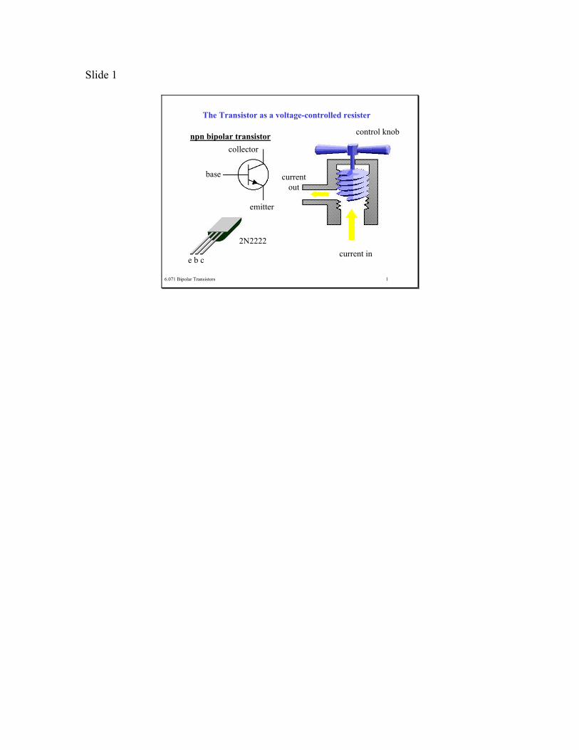
Slide 1
6.071 Bipolar Transistors 1
emitter
collector
base
npn bipolar transistor
The Transistor as a voltage-controlled resister
control knob
current in
currentout
e b c
2N2222

Slide 2
6.071 Bipolar Transistors 2
The Diode
V (volts)
I(A) 0.6V
As described, but turns on at 0.6V (for a Si diode).

Slide 3
6.071 Bipolar Transistors 3
Normally off (base/emitter reverse biased), small input current and voltage relative to emitter turns it on, switching and amplifying
emitter
collector
base
Transistor Properties
IC = βIBIE = IC + IB = (1+ β)IBVBE =VB −VE = +0.6V
β ~ 100, but changes with temperature and with VCE
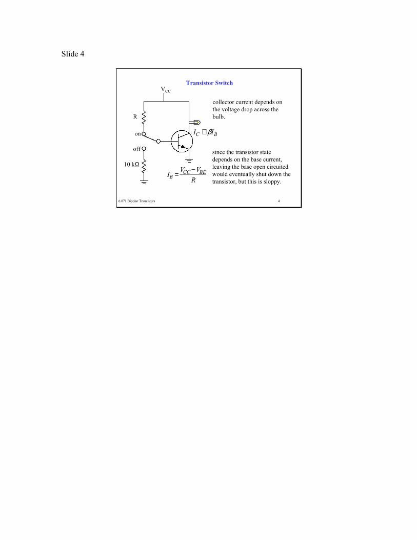
Slide 4
6.071 Bipolar Transistors 4
10 kΩ
Transistor SwitchVCC
R
on
off
IC ≅ βIB
collector current depends on the voltage drop across the bulb.
IB =VCC−VBE
R
since the transistor statedepends on the base current,leaving the base open circuitedwould eventually shut down the transistor, but this is sloppy.

Slide 5
6.071 Bipolar Transistors 5
Transistor Switch
VCC
IB
R
VBE
VCC = IR+VBE
IB =VCC −VBER
IC = β VCC−VBER
VBE =0.6V
Slide 6
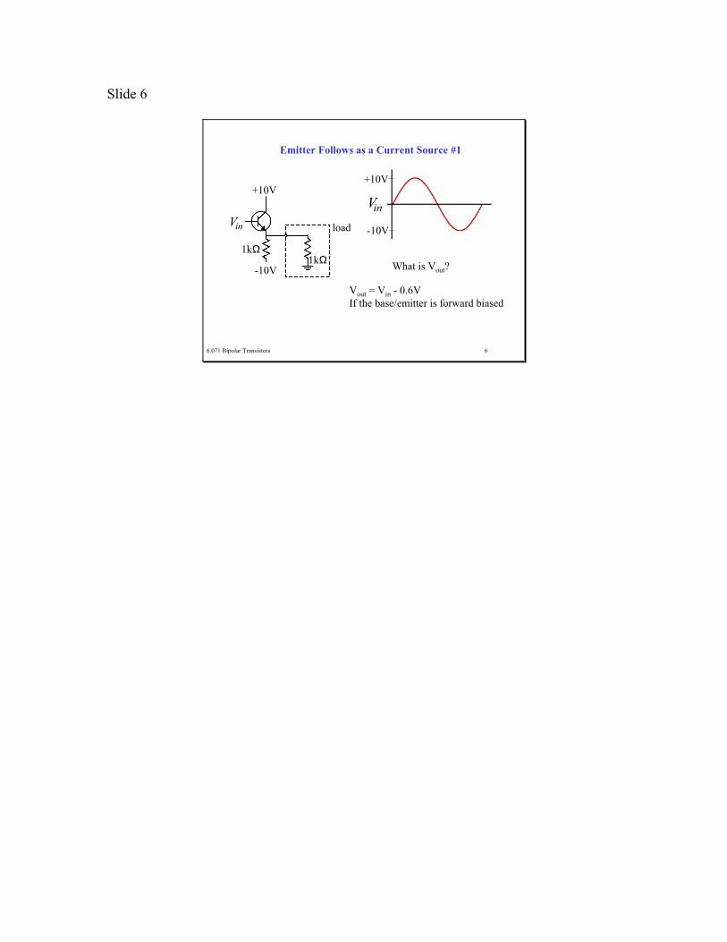
6.071 Bipolar Transistors 6
Emitter Follows as a Current Source #1
Vin
+10V
-10V
1kΩ1kΩ
load
+10V
-10V
Vin
What is Vout?
Vout = Vin - 0.6VIf the base/emitter is forward biased
Slide 7
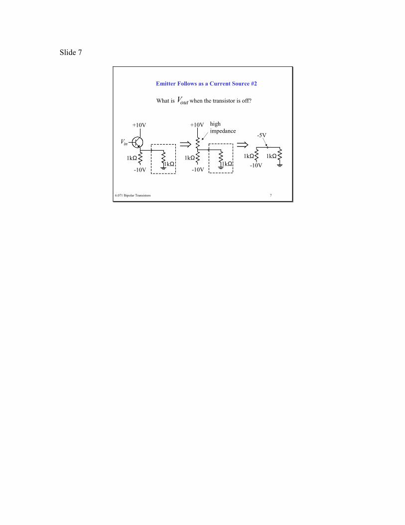
6.071 Bipolar Transistors 7
Emitter Follows as a Current Source #2
Vin
+10V
-10V
1kΩ1kΩ
What is when the transistor is off?Vout
⇒1kΩ 1kΩ
-10V
-5V
⇒
+10V
-10V
1kΩ1kΩ
highimpedance

Slide 8
6.071 Bipolar Transistors 8
Emitter Follows as a Current Source #3
Vin
+10V
-10V
1kΩ1kΩ
At what base voltage does it turn off?
VBE = 0.6V∴ Vin = −4.4V

Slide 9
6.071 Bipolar Transistors 9
Emitter Follows as a Current Source #4
Vin
+10V
-10V
1kΩ1kΩ
+10V
-10V
Vin
Vin
Vout
Vout = Vin − 0.6V;
−5V;Vin ≥ −4.4VVin < −4.4V
Slide 10
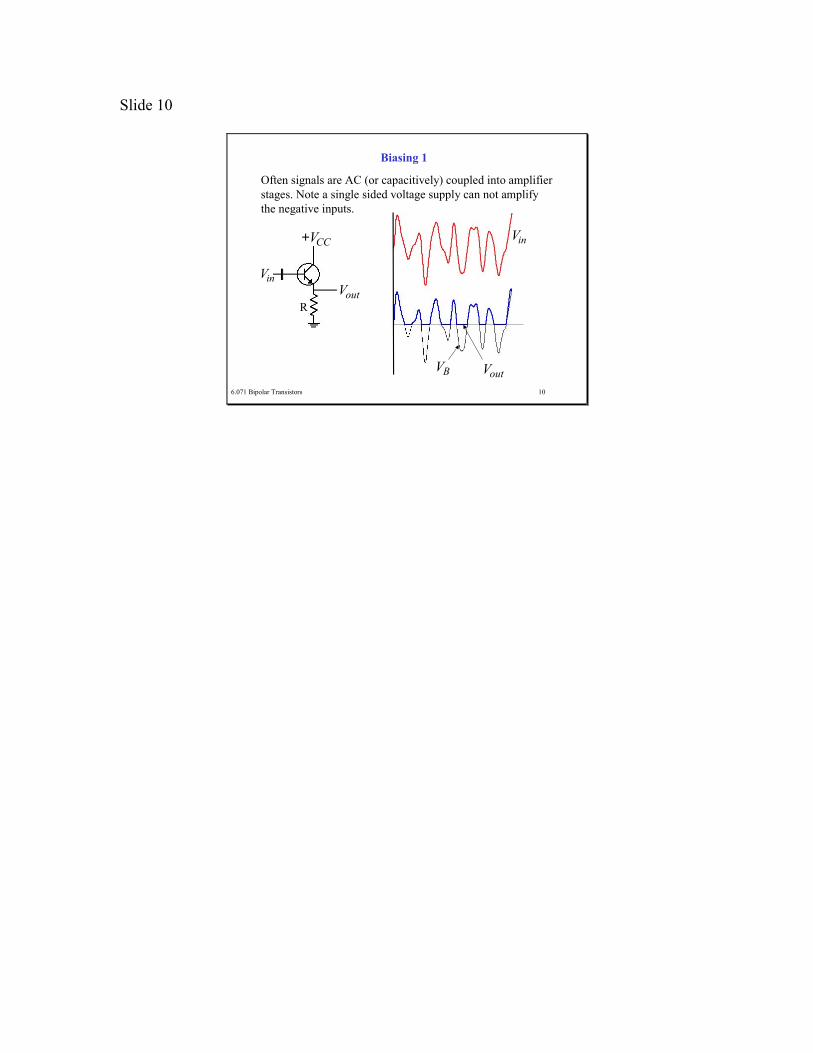
6.071 Bipolar Transistors 10
Biasing 1
Often signals are AC (or capacitively) coupled into amplifierstages. Note a single sided voltage supply can not amplifythe negative inputs.
Vin
+VCC
VoutR
Vin
VoutVB

Slide 11
6.071 Bipolar Transistors 11
Biasing 2
Vin
Solve this by adding a DC to the base to shift the signal so that thereis no clipping and AC coupling the output.
RE
R1
R2
VCC
Vout
select
want
VCC =15V
R1 || R2 <<βRER1|| R2 is the impedance of thecurrent source used to drive the transistor, βRE is the effective impedance of the base of the transistor.
Rule: make the impedanceof the source smallcompared to the loadit drives.
Slide 12
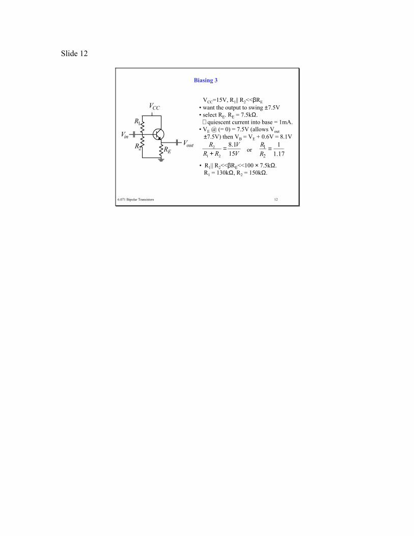
6.071 Bipolar Transistors 12
Biasing 3
Vin
RE
R1
R2
VCC
Vout
VCC=15V, R1|| R2<<βRE• want the output to swing ±7.5V• select RE. RE = 7.5kΩ. ∴ quiescent current into base = 1mA.• VE @ (= 0) = 7.5V (allows Vout
±7.5V) then VB = VE + 0.6V = 8.1VR2
R1 + R2
= 8.1V15V
R1R2
=1
1.17or
• R1|| R2<<βRE<<100 × 7.5kΩ.R1 = 130kΩ, R2 = 150kΩ.

Slide 13
6.071 Bipolar Transistors 13
oscillatorFrequencyamplitude
trigger
Input #1 Input #2
oscilloscopetime-base display
Vout1kΩ
dual voltage source
12V
33kΩ
Vin
time
Vout
time
Vin
Demo: BJT Emitter Follower #1

Slide 14
6.071 Bipolar Transistors 14
Demo: BJT Emitter Follower #2
oscillatorFrequencyamplitude
Input #1 Input #2
oscilloscopex,y display
Vout1kΩ
dual voltage source
12V
33kΩ
Vout
Vin
Vin

Slide 15
6.071 Bipolar Transistors 15
Emitter Follower
VCC
Rload
Rin = βRload
The output voltage is almost the base voltage, with a 0.6 V cutoff. Notice the change in impedance.
VB
Vout =VB − 0.6V

Slide 16
6.071 Bipolar Transistors 16
The Emitter Follows Has Unit Voltage Gain;
Is it Useless?
Vin
+VCC ∆Vin = ∆Vout
−VCC
VoutR
Note: ∆IE =∆VoutR
=∆VinR
and ∆IB =∆IE
1 + β=
∆VinR 1 + β( )
∴ Pin =Vin
2
R(1+ β);Pout =
Vin2
RP = IV
There is a gain in Power of β.
The effective base resistance is βR.

Slide 17
6.071 Bipolar Transistors 17
Don’t design with β
Vin
VCC
VoutRE
βREHere the quiescent point was selected by bleeding a small amount of current into the base.Now the operating point depends critically on β which varies tremendously from device to device and with temperature.
Slide 18
6.071 Bipolar Transistors 18
Problem: Look at last circuit as β is varied from 100 to 200.

Slide 19
6.071 Bipolar Transistors 19
Current SourceVCC
Rload
Iload = IC = VB − 0.6VR
IC ≅ IE , for large β
The base voltage controls the current through the load up to the limit of VCC.
R
VB
VE
VE =VB −0.6V
IE = VER

Slide 20
6.071 Bipolar Transistors 20
Common Emitter #1
The common emitter configuration provides a (negative) voltage gain. (1) Set the quiescent current such that VC = VCC/2 → Want a voltage drop ofVC over RC.
VCC
Vin
RC
VC
RER2
R1
∴ IC = Iq = VCRC
= VoutRC
;
IB = VinβRE
= ICβ
∴ VoutVin
= −RCRE

Slide 21
6.071 Bipolar Transistors 21
Common Emitter
So RC = VCC/(2 Iq).
Gain = -RC/RE
RE is necessary for stability, otherwise there is a small resistance rtr ~ 0.026V/IE, but this is very temperature sensitive.
VCC
Vin
RC
VC
RER2
R1

Slide 22
6.071 Bipolar Transistors 22
Rule for robust control
source load
If the source output impedance is much lower than the loadinput impedance than the circuit performance will beindependent of load variation. Therefore in a multi-stage device, if we use a FET asthe building blocks of the load, the input impedance of the load will be high and we will have a robust circuit.

Slide 23
6.071 Bipolar Transistors 23
Voltage Transfer
VL =RL
RL + RthVth
Rth
RLVth so if VL~Vth
∴ Rth << RL
For efficient voltage transfer, keep the load impedance largerthan the source impedance.
Two exceptions:• Radio Frequency circuits, Zsource=Zload
(provide maximum power transfer)• Coupling currents rather than voltages.

Slide 24
6.071 Bipolar Transistors 24
Current Transfer
IL =RN
RL + RNIN
RLIN so if IL~IN
∴ RN >> RL
RN
IL
For efficient current transfer keep the load impedance smallcompared to the source impedance.
Slide 25
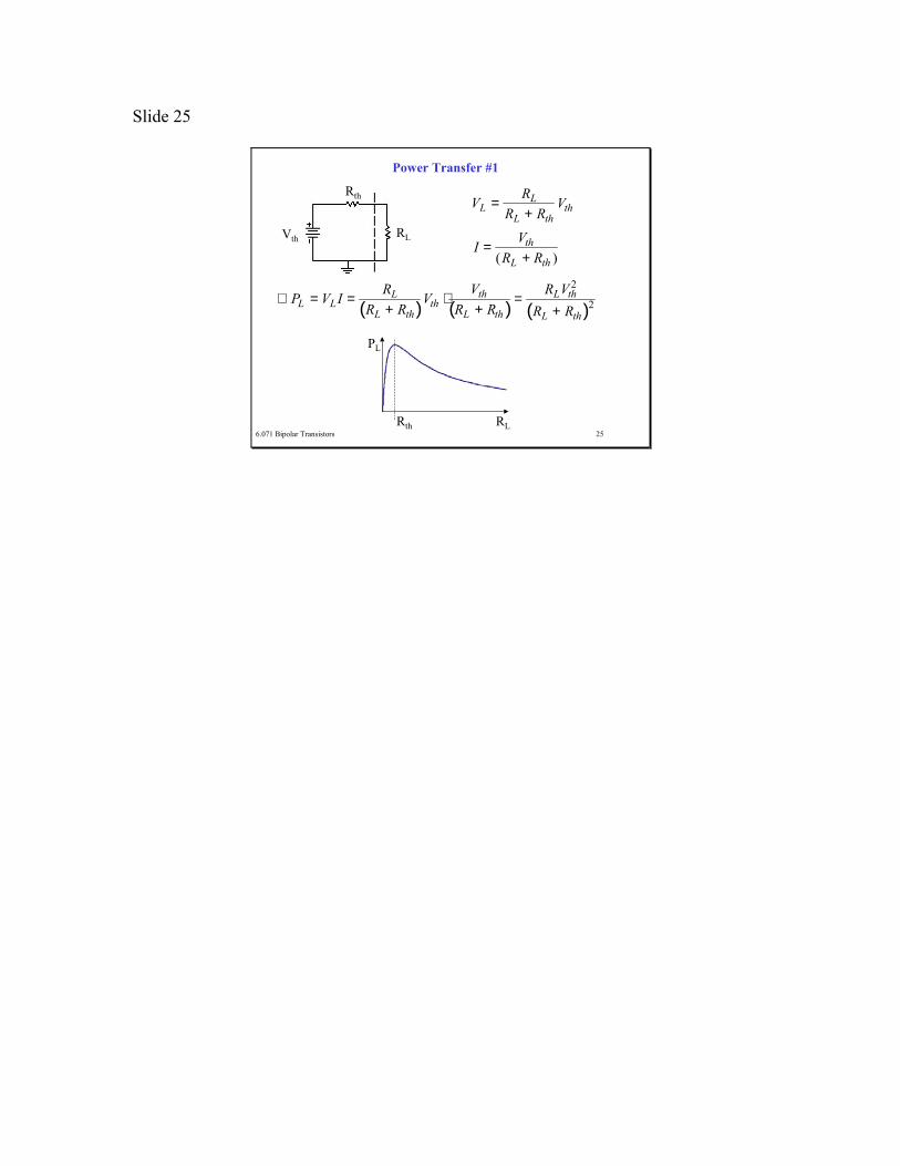
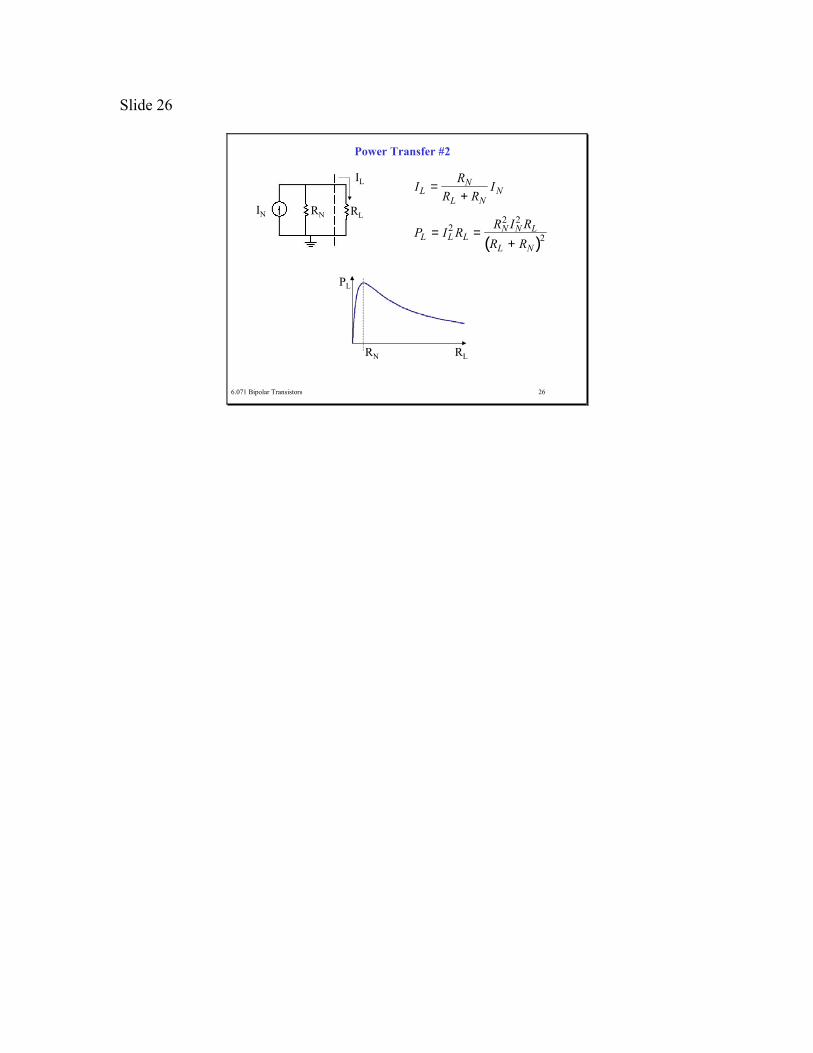
6.071 Bipolar Transistors 25
Power Transfer #1
VL =RL
RL + RthVth
Rth
RLVthI =
Vth(RL + Rth )
∴ PL = VLI =RL
RL + Rth( )Vth ⋅Vth
RL + Rth( ) =RLVth
2
RL + Rth( )2
PL
Rth RL
Slide 26
6.071 Bipolar Transistors 26
Power Transfer #2
IL =RN
RL + RNIN
RLIN RN
IL
PL = IL2RL =
RN2 IN
2 RLRL + RN( )2
PL
RN RL

Slide 27
6.071 Bipolar Transistors 27
Unity-gain phase splitter
Vin (+)
goal: from an AC signal generate a copy and its inverse.
Vout− = −Vin(+)
Vout+ =Vin (+)
4.7kΩ
4.7kΩ
56kΩ
150kΩ
20V
Vout+ ≡
Vout− ≡
emitter follows∴ unity gain
common emitter∴ with RC=RE, gain=-1

Slide 28
6.071 Bipolar Transistors 28
Biasing Unity-gain phase splitter
4.7kΩ
4.7kΩ
56kΩ
150kΩ
20V
15V5V
5.6V
• choose VE = 5V∴ VB = 5.6V
since IC ? IE, there is a dropof 5V over both 4.7kΩresistors.

Slide 29
6.071 Bipolar Transistors 29
Darlington Pair
Useful for large current applications, and high input impedance. They are slow, however. Base to Emitter drop is 1.2 V.
β2
β1β1 β2
Slide 30
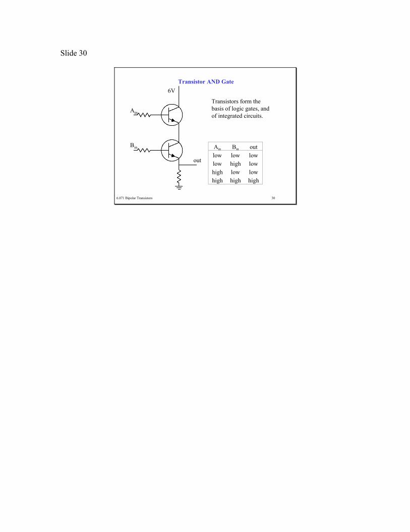
6.071 Bipolar Transistors 30
Transistor AND Gate
Ain
Bin
out
6V
Ain Bin outlow low lowlow high lowhigh low lowhigh high high
Transistors form the basis of logic gates, and of integrated circuits.
Slide 31
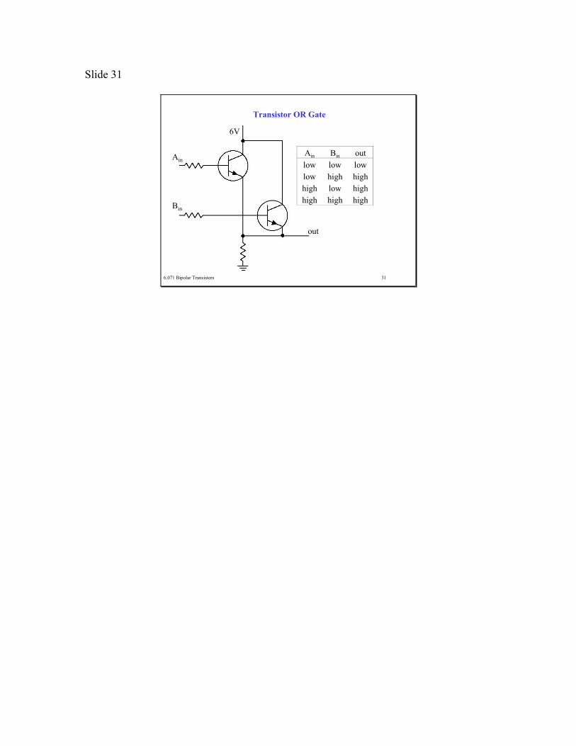
6.071 Bipolar Transistors 31
Transistor OR Gate
Ain
Bin
out
6V
Ain Bin outlow low lowlow high highhigh low highhigh high high

Slide 32
6.071 Bipolar Transistors 32
Properties of Bipolar Transistors
β (current gain) is not a parameter, it varies with everything.
IC,max - maximum collector current rating.
BVCBO - maximum collector to base voltage.
BVCEO - maximum collector to emitter voltage.
VEBO - emitter to base breakdown voltage.
PD - maximum collector power dissipation.

Slide 33
6.071 Bipolar Transistors 33
Datasheet of 2N2222 (1 of 3)
Slide 34
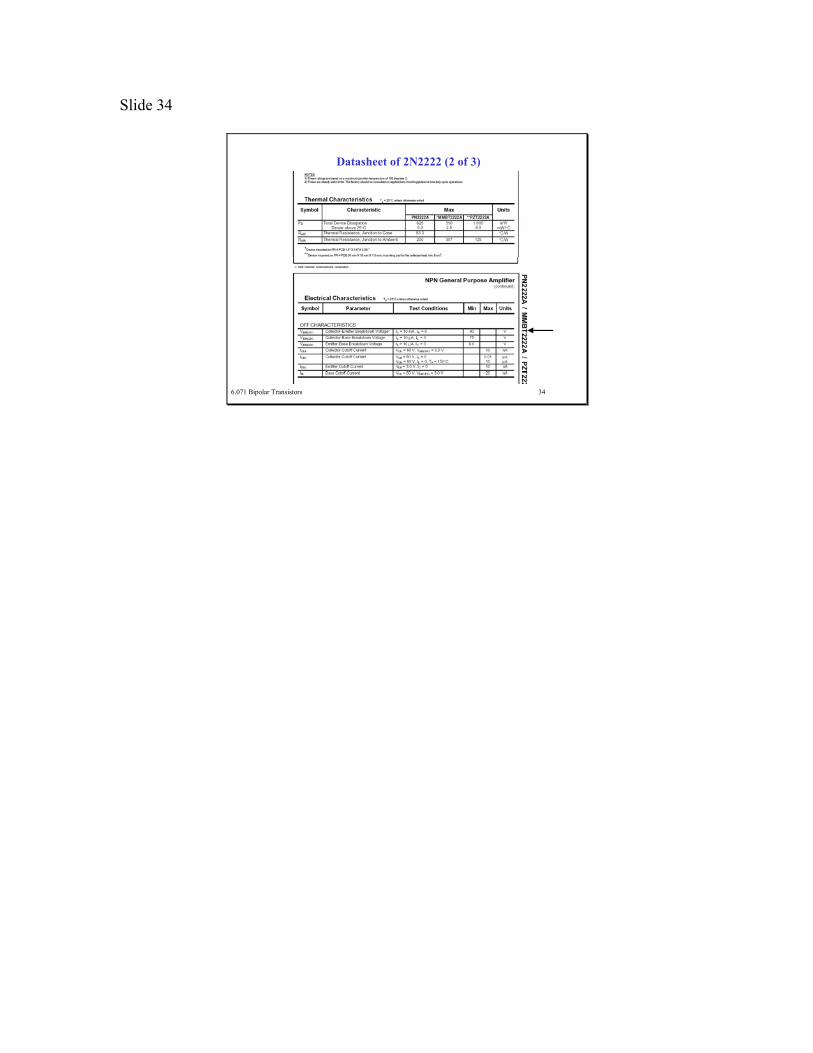
6.071 Bipolar Transistors 34
Datasheet of 2N2222 (2 of 3)

Slide 35
6.071 Bipolar Transistors 35
Datasheet of 2N2222 (3 of 3)

Slide 36
6.071 Bipolar Transistors 36
Voltage Regulator
Vin
Vout = VzenerREA simple voltage regulator.
Poor ripple suppression, requires a zener with high power rating, and variations with load impedance.
RealZener
IdealZener
I
V
Zeners are diodes that have variable resistance. Specifically,zeners have a constant currentoutput over a range of input voltages. Thus, by providing a constant current to a circuit,zeners can be used as voltageregulators.

Slide 37
6.071 Bipolar Transistors 37
Voltage Regulator
Vin
Vout = Vzener-0.6 V
R
Emitter follower configuration.
Base current is only 1/β of supply current.
RC filter reduces ripple.
VzenerC
Rload

Slide 38
6.071 Bipolar Transistors 38
Switching inductive loads
The voltage kick from interrupting current flow in an inductor can lead to voltage breakdown in the transistor. A backwards diode across the inductive load shorts this out.

Slide 39
6.071 Bipolar Transistors 39
Common Collector AmplifierVCC
Rload
An amplifier with a current gain (no voltage gain) and offset to avoid clipping negative inputs.
VB
R1
R2
C1C2
RE
R1 and R2 provide the DC offset and C1 acts as a filter (so inputs do not disturb quiescent point).
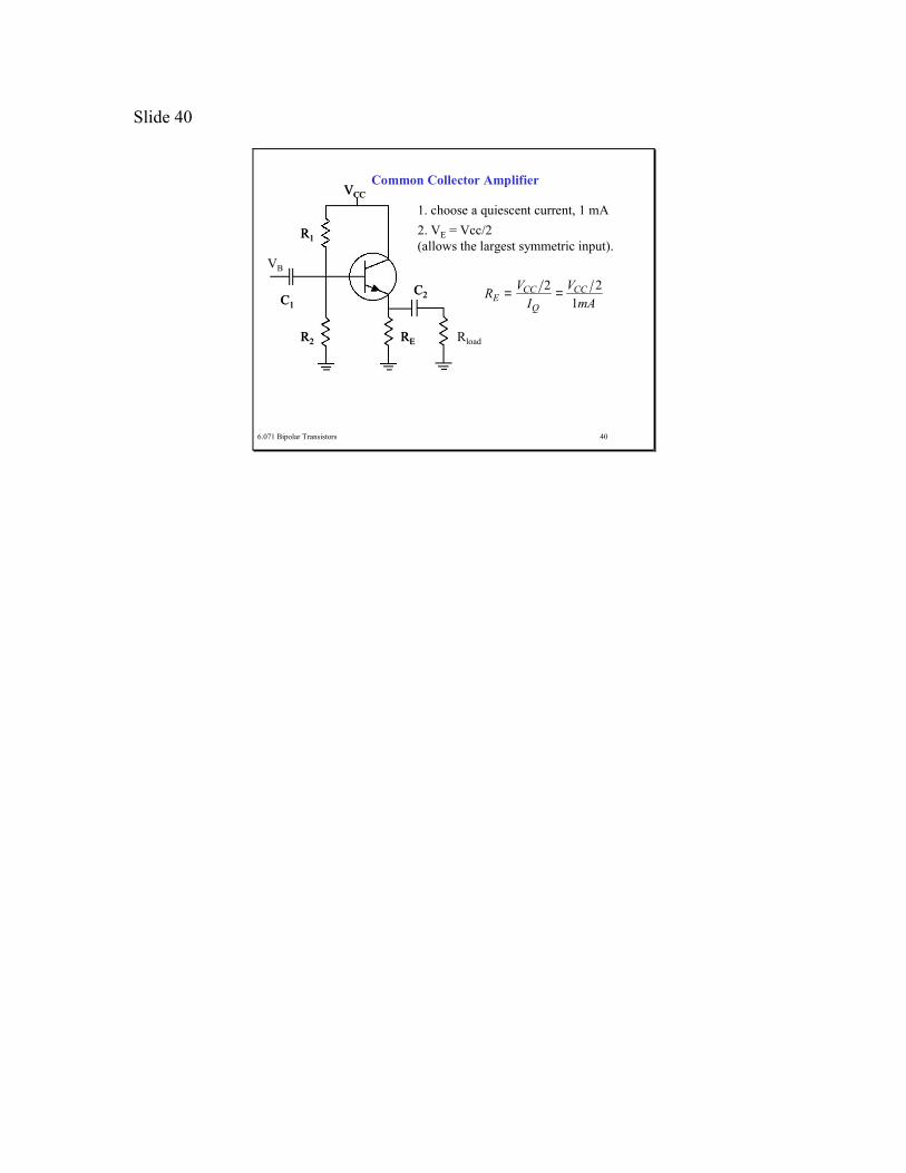
Slide 40
6.071 Bipolar Transistors 40
Common Collector AmplifierVCC
1. choose a quiescent current, 1 mA
VB
R1
R2
C1C2
RE
2. VE = Vcc/2 (allows the largest symmetric input).
RE = VCC 2IQ
= VCC 21mA
VCC
Rload
R1
R2
C1C2
RE

Slide 41
6.071 Bipolar Transistors 41
VCC
Rload
R1
R2
C1C2
RE
Common Collector AmplifierVCC
3. Set the quiescent current via R1 & R2.
R1R2
= VCC −VBVB
= VCC −VE − 0.6VVE + 0.6V
VE =VCC 2recall:
So, forget 0.6V and R1 = R2
Note that Rbase = β RE,
so R1||R2<< β RE
prevents the quiescent point from shifting with load.

Slide 42
6.071 Bipolar Transistors 42
Common Collector AmplifierVCC
Rload
VB
R1
R2
C1C2
RE
4. Choose coupling capacitorsThe effective AC input resistance
Rin = R1 R2 β RE Rload( )C1 and Rin form a high-pass filter
C1 = 1ω3dB Rin
C2 and Rload also form a high-pass filter C2 = 1ω3dB Rload
VCC
Rload
R1
R2
C1C2
RE
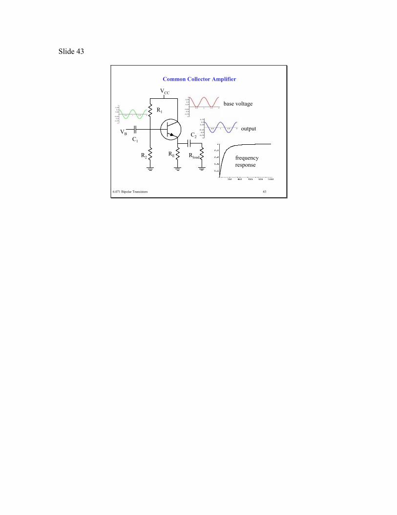
Slide 43
6.071 Bipolar Transistors 43
Common Collector Amplifier
VCC
Rload
VB
R1
R2
C1C2
RE
base voltage
output
frequencyresponse