
The Time of Flight Upgrade for CLAS at 12GeV
68
i The Time of Flight Upgrade for CLAS at 12GeV by Lewis P. Graham Bachelor of Science Benedict College, 2002 -------------------------------------------------------------------- Submitted in Partial Fulfillment of the Requirements for the Degree of Master of Science in Physics College of Arts & Sciences University of South Carolina 2008 --------------------------------------------------- ---------------------------------------------------- Director of Thesis 2 nd Reader --------------------------------------------------- ---------------------------------------------------- 3 rd Reader Dean of The Graduate School
Transcript of The Time of Flight Upgrade for CLAS at 12GeV

i
The Time of Flight Upgrade for CLAS at 12GeV
by
Lewis P. Graham
Bachelor of Science Benedict College, 2002
--------------------------------------------------------------------
Submitted in Partial Fulfillment of the Requirements
for the Degree of Master of Science in Physics
College of Arts & Sciences
University of South Carolina
2008
--------------------------------------------------- ---------------------------------------------------- Director of Thesis 2nd Reader
--------------------------------------------------- ---------------------------------------------------- 3rd Reader Dean of The Graduate School

ii
ACKNOWLEDGMENTS
I thank Professor Ralf Gothe for his help and guidance during this time we
have worked together. His philosophy and approach to physics and research has
inspired me to understand every problem, exhaust every possible solution, and
optimize the appropriate conclusion to extend to all aspects of physics. He is a
great professor and mentor.
I thank Dr. Kijun Park for his extremely valuable feedback and
suggestions.
I thank all my colleagues who helped me working on this study: Collin
Eaker, Dominik Gothe, Evan Phelps, Haiyun Lu, Legna Torres, and Zhiwen
Zhao.
I thank my family P, Mary, Alicia, and Tara for their patience and support.

iii
ABSTRACT
The Time of Flight (TOF) system is a detection system within the CEBAF
Large Acceptance Spectrometer (CLAS) at Thomas Jefferson National
Accelerator Facility. CLAS, being a multi-gap toroidal magnetic spectrometer, is
used in the detection of particles and their varying properties and interactions.
The Thomas Jefferson National Accelerator Facility provides a continuous
electron beam of energy 6GeV, to investigate nuclear reactions by obtaining the
identification and energy of the production particles. The CLAS detector is
designed and currently runs at energies of up to 6GeV, but with recent approval it
will be upgraded to energies of 12GeV. CLAS consists of drift chambers to
determine the charged particle paths, gas Cherenkov counters for electron
discrimination, TOF scintillators for nucleon and meson identification, and an
electromagnetic calorimeter for identifying showering electrons and photons.
The TOF system, which is our focus, is composed of scintillation counters at the
forward angle, and covers an area of 206 meters squared. Therefore, we look to
upgrade and construct the TOF system of CLAS and outline strategies of current
construction, purpose for design, and outlook for the Forward TOF system
upgrade. First results have led to the conclusion that of two timing methods
performed, the Source Method will produce better time resolution results after
further optimization.

vi
LIST OF FIGURES
Figure 1.1: CLAS Detector…………………….……………….………………........3
Figure 2.1: Scintillation and PMT Assembly….……………….……………….......8
Figure 2.2: Light Transmission Simulation….……………….………………........10
Figure 4.1: Cylindrical Cross-section Mu-metal Schematic……………………...20
Figure 4.2: Magnetic Field Effect on Signal Amplitude…………………………...21
Figure 4.3: Square Cross-Section Mu-metal Schematic………………………....22
Figure 5.1: Cable Attenuation Setup……………………….……...………….……24
Figure 5.2: Table of Measured Cable Results…………………………………….24
Figure 5.3: Rise Time vs. Length (10-90% & 30%-70%)….………………….....25
Figure 5.4: Amplitude vs. Length ………………………………………………….26
Figure 6.1: CFD Signal Behavior…………………………………………………..29
Figure 6.2: Signal Amplitude Setup………………………………………..………30
Figure 6.3: Signal Images from PMT, LED, and CFD……………….…………..31

vii
Figure 6.4: CFD Attenuation Schematic............................................................31
Figure 6.5: CFD External Attenuation Image…………………………………......32
Figure 6.6: RMS vs. Delay…………………………………………………..………33
Figure 6.7: Optimized Delay for CFD……………………………………….. …….34
Figure 7.1: TDC Calibration process……………………………………………….36
Figure 7.2: Delay vs. TDC Reading…………………………………………..........37
Figure 7.3: Differential Non-linearity Conceptual Setup…..................................38
Figure 7.4: Differential Non-linearity Electronic Process………………………....39
Figure 7.5: RMS code widths comparison……………………………….…………40
Figure 8.1: Particles Momentum Separation ………………………………………43
Figure 8.2: 3 Counter Method…………………………………………....................45
Figure 8.3: Reference Counter Method………………………………..……………47
Figure 8.4: Reference Method Results……………………………………………...50
Figure 8.5: Source Method…………………………………………………………...52
Figure 8.6: Beam Spot Setup & Distribution………………………………….........54
Figure 8.7: First TDC Resolution………………………………..…………………...55

viii
Figure 8.8: Second TDC Resolution………………………………………………..56
Figure 8.9: Time Walk Parameterization…………………………………………..57
Figure 8.10: Best TDC Resolution …………………….…………………………..57
iv
TABLE OF CONTENTS
ACKNOWLEDGMENTS…………………………………………………………….....ii
ABSTRACT……………………………………………………………………………..iii
LIST OF FIGURES…………………………………..…………………………………vi
1) INTRODUCTION…………………………...…………...………………….…….…1
2) DESIGN OF TOF SYSYTEM……...………….………….………………………..5
2.1) SCINTILLATION MATERIAL..…………………………………………….....5
2.2) PHOTOMULTIPLIER TUBES……………………………………….…….....6
2.3) VOLTAGE DIVIDERS.…………...……………...……………………………8
2.4) LIGHT GUIDES………………………….…….....……………………….…..9
3) ELECTRONICS…………….…………………….………………………………..11
3.1) INTEGRAL DISCRIMINATOR…………… …...…………….……………..14
3.2) SCALER……………………………………………………………….……...15
3.3) COINCIDENCE…………………...……………...…………………………..15
3.4) TIME-to-DIGITAL CONVERTER (TDC)…….....……………………….….16
3.5) ANALOG-to-DIGITAL CONVERTER (ADC)…..…………………………..17
4) MU METAL SHIELDING TESTS………….…..………………….……………...19
5) CABLE DELAY and RISE TIME TESTS……..………………….……………...23
6) DISCRIMINATOR TESTS………..…………….………………………………...27
7) TDC CALIBRATION and LINEARITY.……………..…………...………………..35

v
8) TIME RESOLUTION………………………..…………………...…………………42
8.1) 3 COUNTER METHOD.……….……………….……..………………..44
8.2) REFERENCE COUNTER METHOD…………….……..……………..47
8.3) SOURCE METHOD…………….……………….……..……………….50
9) CONCLUSIONS……………………………………………………………………58
LIST OF REFERENCES……………………….…………………..…………………60

1
1) INTRODUCTION
The thrust of modern experiment embodies the study of the nucleon
through exclusive and semi-exclusive processes to provide new insights into
nucleon dynamics down to the elementary quark and gluon level. Through
inclusive scattering of high-energy leptons off the nucleon, primary investigations
into the internal structure of the nucleon have been performed for many years.
These inclusive measurements are insensitive to the internal quark-gluon
dynamics; furthermore they provide a one-dimensional image of the quark
longitudinal momentum distribution. With these inclusive measurements at
current availability, the demand to date is for various exclusive measurements
into nucleon dynamics. Thus, the precedent for the CLAS 12 GeV upgrade is
valid, and needed to move the study of the internal nucleon dynamics to the next
level.
The CLAS 12 detector is an evolution of the present CLAS to meet the demands
for advance studies into the structure of nuclei. The upgrade will be required to
provide access to generalized parton distributions in exclusive reactions. To
adequately foster these needs, CLAS 12 will need to accommodate a higher
energy, and a higher luminosity continuous electron beam. The two major
components of the upgrade are the existing Forward Detector and a new Central
Detector to be installed around the target. Thus, our present agenda is to focus

2
our work on the Forward Detector portion. The Forward Detector detects neutral
and charged particles from angles of 5° up to 40°. Presently, it consists of 7 main
sub-detectors for the precise detection of particles.
Figure 1.1 shows the present CLAS detector and all the components. The first
important feature of the Forward Detector is a toroidal magnet to produce an
azimuthally symmetric field. The toroidal magnet does not really serve as a unit
of detection but more a device for manipulating particle trajectories and paths
according to their momenta. The first components of the Forward Detector are
drift chambers (DC), used to acquire the trajectories of charged particles.
Cerenkov Counters (CC) make up the second component housed in the Forward
Detector. They are used to discriminate electrons from all production particles of
the various reactions. The third component, Scintillation Counters (SC),
determine the time of flight for particles traveling from the target to the detector.
After the scintillation counters comes the Electromagnetic Calorimeters (EC)
which are used in detecting showering particles. These make up the fourth
component of the detector. The next important feature would be the two-level
trigger system contained by the Forward Detector. This system initiates data
conversion and fast readout. The Data Acquisition (DAQ) is the final important
feature of the detector where it collects all digitized data and stores it for later
analysis. Amongst the 4 components that make up the Forward Detector, the
TOF system inherits our focus for the upgrade of CLAS at 12GeV.

3
Figure 1.1: CLAS Detector1.
The Time of Flight (TOF) system is designed to decipher the flight time of
particles produced from incident radiation reactions. If a particle’s start position
and momentum are known by taking the path length information to where it was
detected in TOF, one can calculate the velocity of that particular particle. The
time of flight system at CLAS uses the start time arrival time of a particle to
govern its flight time. The system was purposed to include good timing
resolution to adequately identify particles and also obtain good segmentation to
provide flexible triggering and pre-scaling. The time of flight system is subdivided
into two groups which are parameterized by the scattering angle of the reaction
particle. At angles of 0° to 40°, TOF is comprised of what are known as the small
(forward) angle counters. At these angles, the scattering angle is minimal and
the particle inherits more momentum. From 41° and above, these are known as
1 The Diagram show the different components that make up the CLAS detector.

4
the large angle counters. One important advantage of the reconstructed angles
is depending on the orientation of the magnetic field, the bending angle provides
immediate information as to the charge of particles within the reaction. The TOF
system is equipped for a resolution of σ = 120ps at the smallest angles and
250ps at angles of 90° and larger. These specifica tions are required by the fact
that at small angles, the most energetic particles are produced requiring a better
resolution where this lessens with each increment in the angle. Using off-line
analysis, the identification of particles is achieved by correcting leading-edge
discriminator based time measurements with pulse-height information for the
introduced time-walk. Thus, the system is required to give signals that represent
a uniform response to selected particles that reach the time of flight detectors.
The TOF system is not only used to determine the particles’ velocity but can also
be used for energy-loss measurements. Energy loss in the counter is
proportional to pulse-height information which means there is a separate way to
identify slow particles. If multiple scattering particles dominate the tracking
resolution, then the particle’s distinct energy loss can also give a better
measurement of particle energy. In addition to excellent timing resolution and
segmentation, the TOF system has to be able to operate in a high-rate
environment. Being that all detectors must be optimized for best results, the time
of flight system for CLAS is one of several detector subsystems being upgraded
to unveil new and exciting physics. For this reason, we have taken on the
challenge and lead in prototyping and eventually building the new time of flight
system that will operate at 11GeV.

5
CHAPTER 2: DESIGN OF TOF SYSTEM
2.1) SCINTILLATION MATERIAL
The most important and vital component within the detection system is the
scintillation material. The scintillator provides a small flash of light or
“scintillation” when struck by a particle or nuclear radiation. Radiation passing
through the scintillator bar excites the molecules that make up the material. The
excitation comes on absorbing the energy from the incident radiation, where the
scintillator undergoes excitation to a higher electron state followed by a prompt or
delayed return to the ground state. Once these molecules are excited, then light
is emitted and propagates through the scintillation material. This light is then
converted into a current of photoelectrons by a photomultiplier tube (PMT), where
the current signal is enhanced providing easier detection.
In our prototype testing Bicron BC-408 plastic scintillators, which are currently
used in the existing time of flight detector at Jefferson Lab, were used in the time
resolution measurement. The basic premise of our method is to first reproduce
the time resolution gained in the previous prototype for CLAS at 6 GeV.
Reproducing this resolution or obtaining a better value would give us validable
consistency in our setup and electronics. Thus changing additional hardware
such as scintillation material and PMTs will help improve the timing resolution.

6
Scintillators are excellent testing material because of the information their signal
can provide. They are extremely sensitive to energy, in that the light output is
directly proportional to the energy loss.
Scintillation detectors have a fast timing response and recovery rate. The fast
response allows superior accuracy in the collected timing information, and the
quick recovery allows more data to be taken due to less time being demanded
between events. The advantages of using a plastic scintillator are numerous.
They provide extremely fast signals and an immense light output. The plastic
bars are easily mechanized because they are flexible under the right amount of
pressure. This is key in the setup because it provides connectivity options to
either light guides or directly to the photomultiplier tubes (PMT) for greater
precision.
2.2) PHOTOMULTIPLIER TUBES
In nuclear and high-energy physics, PMTs are widely used in scintillation
detectors. PMTs are electron tube devices which convert light into an electric
current that can be measured. They consist of a photocathode made of sensitive
material for photon-electron conversion. The photocathode is followed by a
collection and multiplication system for electrons. The photocathode consists of
a material with a low work function, simply meaning its ionization energy is low
enough for visible or ultra-violet photon energies to create a free electron and
give enough kinetic energy to escape from the surface region. From the

7
scintillator, an incident photon impinges upon the photocathode which produces
the emission of an electron by the photoelectric effect. The applied voltage then
directs and accelerates the electron to the first dynode. Secondary electrons are
emitted from this dynode and directed and accelerated to the next dynode, and
so on this process continues creating a shower of electrons. The anode collects
this cascade of electrons which produces a typical analog current of 40mA for
further measurement and testing in the electronic chain. After amplification
through the multiplier structure, a typical scintillation pulse will give rise to
2.5X10¹⁰ electrons, sufficient to easily serve as the charge signal for the original
scintillation event. Figure 2.1 shows the schematics of a PMT and how the
incident photon produces the electron avalanche passing through the dynode
layers.
The XP2020/UR PMTs were chosen in our prototype experiment. These tubes
possess a faster rise time over the existing tubes used in the CLAS detector
today.

8
Figure 2.1: Schematic of the photon process as light propagates through scintillation into the photomultiplier tube and through the various components of the tube 2.
Once a signal is passed through the PMT diagram, it can be taken from two
points, the anode and the last dynode. The anode signal is larger than the
dynode signal since it is multiplied by one more stage. The anode signal will be
used for triggering, while the dynode is used for measuring the amplitude signal.
2.3) VOLTAGE DIVIDERS
Dividers use high-voltage field effect transistors to fix the PMT gain by
stabilizing the voltage even at high signal rates, and to protect the PMT against
too high light levels where they would shut down the circuit if such an over-
current would occur. We utilized VD127K [8] voltage dividers in our
measurements.
2 Diagram displays scintillation counter attached to photomultiplier tube and the process a photon goes through once it reaches the tube.

9
2.4) LIGHT GUIDES
A light guide plays the role of mediator between the scintillation material
and the photomultiplier tube. Light guides are used to connect the scintillators to
the PMTs to optimize the light transmission. For various reasons, such as oddly
shape scintillation or magnetic field presence, light guides may be needed. The
light guide provides transmission by relying on total internal reflection of the light
signal through its internal walls from one end to the other. For our purpose, a
light guide for the shape adaptation between the PMT and scintillation bar is not
needed. In our prototyping, we had simulation done to take into account the loss
due to reflections at the interfaces of the glass envelope of the phototube to the
light guide and the light guide to the scintillator. In Figure 2.2, the ratio in
percentage is shown of the light that has entered the light guide to the amount
that enters the glass envelope of the PMT.

10
Figure 2.2: Simulated results of light transmission (%) into photomultiplier tube with respect to light guide length 3.
As we see in Fig. 2.2, light transmission versus the length of the tube where z=0
would be the tube directly connected to the light guide. The 70% represents
aluminized mylar film and the 90% is for 3M plastic foil. From the simulations, we
see that we increase light transmission into the glass envelope of the PMT
directly attaching the PMT to the scintillation. This will be one of the setups that
we test along with different geometrical shaped light guides.
3 Diagram displays the percentage of light that would be transmitted into the glass envelope of the photomultiplier tube with respect to having a light guide attached. The z axis represents the length of the light guide, where z=0 would be no light guide.

11
CHAPTER 3: ELECTRONICS
Nearly all nuclear and particle physics experiments today utilize data
acquisition systems that are controlled or monitored by computers. These
computer controlled systems are for the most part the mandate of modern
measurements and experimentation in nuclear physics. These mandates vary
from the significant amount of data needed to be processed by a fast, capable
system to the necessity of efficient validating by results from studies. The
processing system used in our experiments and testing is a Computer
Automated Measurement and Control system (CAMAC). This system acts as an
interface between the equipment utilized in the lab and the computer. A CAMAC
“crate” as it is known, physically consists of about 20 slots or stations for plug-in
module instrumentation. The system also has a controller module that allows
each individual module to be operated and controlled by an external computer
through an interface application.
The primary application of the CAMAC system is data acquisition, but it may also
be used for remotely programmable trigger and logic applications. The major
advantage of the housed module instrumentation in the CAMAC is the ease it
provides through the Global Positioning Interface Board (GPIB), and the speed it
has in local data manipulation. Its function is to provide a scheme to allow a wide

12
range of modular instruments to be interfaced to a standardized backplane called
a DATAWAY. Within the crate, each connector provides access to the dataway,
which is a data highway consisting of conductor busses for digital data, control
signals, and power. Module and CAMAC communication takes place through the
DATAWAY control of the CAMAC system. Through the DATAWAY, commands
and data are transferred between system, modules, and controller. Thus, the
system standard precisely covers the electrical and physical specifications for the
modules in use, instrument housings or crates, and a crate backplane. In this
way, additions to a data acquisition and control system may be made by plugging
in additional modules and making suitable software changes. Thus, CAMAC
allows information to be transferred into and out of the instrument modules.
The CAMAC in our case helps to interpret the signals outputted from the
photomultiplier and sends this information to the computer in an understandable
format. It correlates these signals but also measures the signal strength which
gives the charge that the PMT delivered, telling us the overall gain.
For radiation detector applications operated in pulse mode, the detector output
has to be converted to a linear pulse where the shape and amplitude will carry
information of the experiment. Prior to being recorded, this linear pulse may be
administered in the signal chain or converted into a logic pulse to obtain other
information. In the signal chain, an assortment of electronic units are used to
perform a wide range of functions from providing a linear pulse output to the
CAMAC system, to converting the linear pulse to a logic pulse for further
analysis.

13
The primary application of the CAMAC system is data acquisition, but it may also
be used for remotely programmable trigger and logic applications. The major
advantage of the housed module instrumentation in the CAMAC is the ease it
provides through the Global Positioning Interface Board (GPIB), and the speed it
has in local data manipulation. Its function is to provide a scheme to allow a wide
range of modular instruments to be interfaced to a standardized backplane called
a DATAWAY. Within the crate, each connector provides access to the dataway,
which is a data highway consisting of conductor busses for digital data, control
signals, and power. Module and CAMAC communication takes place through the
DATAWAY control of the CAMAC system. Through the DATAWAY, commands
and data are transferred between system, modules, and controller. Thus, the
system standard precisely covers the electrical and physical specifications for the
modules in use, instrument housings or crates, and a crate backplane. In this
way, additions to a data acquisition and control system may be made by plugging
in additional modules and making suitable software changes. Thus, CAMAC
allows information to be transferred into and out of the instrument modules.
The CAMAC in our case helps to interpret the signals outputted from the
photomultiplier and sends this information to the computer in an understandable
format. It correlates these signals but also measures the signal strength which
gives the charge by the PMT delivered, telling us the overall gain.
For radiation detector applications operated in pulse mode, the detector output
has to be converted to a linear pulse where the shape and amplitude will carry
information of the experiment. Prior to being recorded, this linear pulse may be

14
administered in the signal chain or converted into a logic pulse to obtain other
information. In the signal chain, an assortment of electronic units are used to
perform a wide range of functions from providing a linear pulse output to the
CAMAC system, to converting the linear pulse to a logic pulse for further
analysis.
3.1) INTEGRAL DISCRIMINATOR
The first module used in the signal chain is a leading edge discriminator,
where its function is to convert an analog signal into a logic signal. A linear pulse
enters the discriminator which is set to a pre-determined threshold. Once the
input amplitude exceeds the set discrimination level, it is converted into a logic
pulse. As alluded to by Knoll G., 1979 [5], “In order to count the pulses properly,
the linear pulses must be converted into logic pulses.” The discriminator is the
simplest unit which can be used for this conversion. After the “leading edge” of
the linear pulse crosses the discrimination limit, a logic signal is produced to
count and time the linear pulses. This is known as “leading edge timing” and is
the basic timing we used for our measurements. The key to maximizing
measurements with this module is to set the threshold level just above the
system noise. In so doing, we maximize its sensitivity for counting detector
pulses of all sizes to ultimately enhance the signal-to-background counting ratio.
According to Knoll G., 1979 [5], “The stability and linearity of the discriminated
adjustment are usually adequate for routine applications but may become
important specifications for demanding situations.” Simply, the discriminator
reads a signal and decides if it is strong enough to be the actual signal or if it is

15
simply noise. If it is determined to be strong enough and above the set
threshold, then the signal is passed to the next component in the signal chain.
3.2) SCALER
For adequate counting procedures in the measurement, the logic pulses
must be accumulated and the total number recorded over a fixed interval of time.
The scaler performs this process where a simple digital register is incremented
by one count each time a logic pulse is received as an input. Scalers are
typically operated in one of two modes: preset time and preset count. The
counting period is controlled by an external timer in the preset time mode. In the
preset count mode, pulses are accumulated until a certain amount is achieved
thus ending the counting interval. This latter method was used in our resolution
measurements and will be explained in detail in the resolution chapter. Overall,
the scaler simply counts the number of signals it receives for a set time period, a
set maximum count, or until it is manually stopped.
3.3) COINCIDENCE
For coincidence systems, one of the signals serves as a “gate” for the
other incoming signal. The gating pulse must be shaped to define exactly its
start and end time. Eichholz G., 1979 [3] states that the second signal may
contain information on the initiating particle and functions to pass the gate if it
arrives during the appropriate interval without undergoing any shaping itself. The

16
overall purpose of the coincidence system is to distinguish signal from
background events. The principle interest for coincidence circuits is the
simultaneity of events recorded by different detectors or traveling along different
electronic pathways. The need therefore arises to have these separated events
correlate for a common purpose in the electronic chain. Two events are said to
be simultaneous if the interval between them is too short for them to be
distinguishable. Events are rejected or seen as not simultaneous if their time of
separation exceeds the resolving time of the circuit.
The coincidence functions to accept logic pulses of two or more inputs. The
module is defined by the user to accept pulses within the given time interval, and
when a preset number of input pulses are received during this time interval then
a single logic pulse is outputted and passed on to the next component.
3.4) TIME-to-DIGITAL CONVERTER
A time-to-digital converter is a circuit that can convert a time interval
between two pulses (usually digital signals) directly into a digital number
proportional to that time interval. The simplest method of achieving this utilizes a
high frequency oscillator. The oscillator is then started and stopped by the
pulses, and the time resolution is then confined by the frequency of the oscillator.
17
To obtain a digital time interval measurement, the most direct method is to utilize
the stable oscillators and counting methods. The module that performs this logic
function is known as a time-to-digital converter (TDC). The basic concept of this
method is that a digital signal coming from the coincidence module acts as a
START signal for the TDC module to begin counting a constant frequency
oscillator or more simply to start a clock. A second signal, that is appropriately
delayed, coming from a discriminator logic unit serves as a STOP signal and a
counting value is produced which is directly proportional to the time interval being
recorded.
Once a STOP is received, the scaler and timer both are gated off, and the
readout system is triggered by an interrupt signal. After the readout is
successful, it generates a CLEAR signal to the timer window and the scaler. The
system then awaits another event to carry out the process again. The timing
system for a TDC module is completely adequate in timing efficiency for
resolution testing. Not only does it hold these set parameters for processing an
event, but it contains likewise signal generation to CLEAR and re-START the
TDC, scaler, and timing window units upon a hang up or block in the system
during measurement.
3.5) ANALOG-to-DIGITAL CONVERTER
The analog-to-digital converter (ADC) is responsible for converting all
analog signal information into a digital form. The function of the ADC is to derive

18
a digital number that is proportional to the integral of the input signal. The
resolution of the ADC depends on the range of digitization, in that, the higher the
digitization capability of the module, the greater the resolution obtained.
The performance of the ADC is characterized by several parameters. The first,
being its linearity of the conversion. Simply stated, the consistency in the digital
signal is directly proportional to the integral of the input signal. Thus the ADC
can provide direct information as to the energy distribution of the radiation source
or the energy loss of a charged particle passing through the scintillator. (An
advantage of the ADC unit is having one to one correspondence in the energy to
signal integral.) Thus an important aspect is to monitor and test the linearity of
the module. The second parameter would be the conversion speed from analog
to digital information. In this instance our purpose and experimental setups
demand fast measurement; therefore the ADC must contain a high or relatively
adequate conversion rate sufficient for fast measuring.

19
CHAPTER 4: MU-METAL SHIELDING TESTS
In the Forward TOF PMTs face a separate obstacle in addition to
operating for high volume rates with an adequate efficiency. They must also
resist the influence of stray magnetic fields which come from the torus magnet.
To protect the phototubes from these field strengths, magnetic shielding must be
incorporated into the overall design of the TOF system. In our prototype, we
performed tests using the existing mu-metal shielding geometry and thickness for
CLAS. The shielding must protect the PMT from dominantly axial fields but also
from transverse magnetic field components. Smith E., 1999 [6], cites that the
TOF scintillation counters are presently about 5m from the area of the target and
in a local field of less than 10G. So our purpose was to test mu-metal shielding
at different magnetic field strengths for PMTs.
We had a cylindrical mu-metal geometry fabricated with a thickness of 1mm to
match the existing shielding at CLAS.

20
Figure 4.1: Schematic of Cylindrical mu-metal fabrication 4.
With this shielding, we had an end cap to improve the shielding of the axial
component of the field. Fig. 4.2 shows the results from our measurements.
4 Diagram displays the two-dimensional view and dimension of the cylindrical mu-metal fabrication with sealed end cap.

21
Figure 4.2: Images of Signal amplitude with respect to magnetic shielding5.
From the images, we found that the amplitude of the signal is greatly affected
without using any shielding for the PMTs. With shielding the axial field’s
influence on the amplitude of the signal is greatly reduced, and with an end cap
even more. Our study of the mu-metal shielding has solidified the belief that the
PMTs must have shielding because of the negative influence of the magnetic
5 First image shows affect of magnetic field on signal amplitude with no shielding on PMT. Second image shows affect with shielding but no end cap. The third image shows magnetic field effect with shielding and end cap.

22
field. Also, it has given us new ideas in how to adequately accomplish this goal
with an optimal design. For future measurements, we have designed a square
cross section of mu-metal with a sealed end cap.
Figure 4.3: Schematic of Square mu-metal fabrication 6.
This geometry will allow us to stack square pieces of 1mm thickness onto the
shielding to test the best thickness for optimal shielding, more so to allow flexible
additions in the stacking region where the PMTs are staggered.
6 Diagram displays the three-dimensional view and dimensions of the square mu-metal fabrication with sealed end cap for future testing.

23
CHAPTER 5: CABLE DELAY & RISE TIME TESTS
The consistency of the electronic chain is vital to all measurements
performed for prototyping. In several timing applications and measurements, the
need will arise to utilize delays at some instance of the electronic chain of the
signal production. These delays are generally needed to adjust timing mandates
or simply to perform calibration. For delay gain, coaxial cables are used to
connect the various modules providing a desired transit time of the logic signal
along the electronic chain. Since many of our operations required additional
delay, we performed a series of measurements on various coaxial delay cables
to test their efficiency and capabilities.
The first measurement we carried out was the attenuation through the
cable delays. Five separate types of coaxial cable, RG-58, RG-214, RG-8, RG-
9913, and RG-174, were used in this test. The method consisted of running a
periodic signal through a leading-edge discriminator (LED), and the cable in
testing. Then the signal was outputted to an oscilloscope for analysis.

24
Figure 5.1: Cable Attenuation Schematic7.
Cable Type
Cable Length
Delay Time
Signal Speed Amplitude
Rise Time (30% to 70%)
Rise Time (10% to 90%)
Oscilloscope Image
RG-9913
251.5 ft. 303.7 ns 25.24 cm/ns
1.4 V 1.78 ns 10.55 ns RG-9913
RG-8 202.2 ft. 310.6 ns 19.84 cm/ns
1.432 V 2.69 ns 12.69 ns RG-8
RG-174
128.2 ft. 198.35 ns
19.7 cm/ns
1.072 V 4.30 ns 18.03 ns RG-174
RG-214
95.3 ft. 147.4 ns 19.71 cm/ns
1.464 V 1.36 ns 7.01 ns RG-214
RG-58 200 ft. 323.3 ns 18.86 cm/ns
1.32 V 5.67 ns 22.04 ns RG-58
None - - - 1.52 V .836 ns 2.37 ns Direct Input
Figure 5.2: Table of Measured Cable results8.
7 The Diagram shows a Philips (PH) pulse generator (PG) generating random pulses into a leading edge discriminator (LED) through different cables to be tested, RG-58, RG-8, RG-9913 and RG-214 into the oscilloscope (OSC).

25
The rise time for each signal was measured for 10%-90% and 30%-70% of the
leading edge of the signal.
Figure 5.3: Rise Time vs. Length at 10%-90% and 30%-70%.9
8 Table shows the tested properties of the various cables studied. Endnotes continued on the next page

26
For each cable, the amplitude and the signal transit time through the cable were
measured. From these parameters, the speed of the signal through the
Figure 5.4: Amplitude vs. Length for RG-58 cable 10.
cables were determined. Our choice of cable for delay was the RG-58. Using
this particular cable, lengths were varied from 100ft to 500ft and the resulting rise
time and amplitude versus the lengths of the cable were measured.
9 Figures show 10% to 90% and 30% to 70% of RG-58 cable rise time versus the cable length. The rise times are in nanoseconds (ns) and the length is in feet (ft). 10 Figures show RG-58 cable amplitude versus the cable length. The amplitude is in volts (V) and the length is in feet (ft).

27
CHAPTER 6: DISCRIMINATOR TESTS
Discriminators are a useful tool in fast-timing applications and
measurements. The main advantages of discriminator logic units are to count
narrow pulses at very high rates, and to earmark the arrival time of these pulses.
The standard design for the discriminator unit is to work with negative pulses
from the anode of the photomultiplier tube being directly passed through a
properly terminated 50Ω coaxial cable. The analog input pulses that satisfy the
threshold of the discriminator are converted to logic pulses at the output of the
timing discriminator. Thus these pulses can then be processed by a counter or
TDC.
Our prototype goal is to achieve the best time resolution possible. For this
reason we must utilize the most adequate discriminator within our electronic
chain of modules. To carry out this utilization, we compared the operation and
efficiency of the Leading Edge Discriminator (LED) versus the Constant Fraction
Discriminator (CFD). Both these logic units accomplish the conversion of analog
signals to digital signals, but they meet this task by two separate means. The
LED generates a logic signal on the “leading edge” of the analog pulse signal
that passes the pre-set threshold. This, however, potentially incorporates
problems into the timing. If the rise time of the analog pulse of the discriminator

28
remains the same but the amplitude has changed, a shift or “walk” of the
measured time occurs. This “time-walk” as it is called, comes about when you
have two pulses that have the same rise time and different amplitudes. The
pulse with the smaller amplitude will cross the LED threshold at a later time
because the rise times are the same. Thus, this change in amplitude shifts the
timing of the output digital signal by an amount that depends on the amplitude
change. Therefore, the timing must be corrected for time walk when utilizing an
LED.
For the CFD, these timing problems are not inherited by the module in that it
compares a constant fraction of the analog signal and the signal itself to
determine precisely the timing of the output digital signal relative to the input
signal. The CFD splits the input signal and attenuates one part to a certain
fraction of the original amplitude. It then inverts and delays the other part of the
signal before both are summed together. After the attenuated part and the
inverted-delayed part are added together, the zero crossing will give the time of
the output signal created by the CFD. Herein lies the need to perform tests on
both logic units to decipher the greatest productivity between them.

29
Figure 6.1: CFD Signal Behavior11.
The CFD was analyzed to judge the best utilization method for the unit. The
testing method consisted of using three pulse attenuators separate from the
internal attenuation in the module, to witness the signals behavior.
11 The Diagram shows the original pulse is delayed, inverted and added to an attenuated copy of the prompt pulses
.

30
Figure 6.2: CFD Signal Schematic12.
For effective testing, the delay of the signal produced by the external attenuator
had to be measured and corrected appropriately.
12 The Diagram shows the method for producing Fig. 6.2.

31
Figure 6.3: Constant Fraction Discriminator image from oscilloscope13.
To find the additional external delay values, the measurements were taken
without and with all utilized external attenuator combinations.
Figure 6.4: Constant Fraction Discriminator Attenuation Schematic14.
13 The image shows the signal that goes directly to the scope from the logic fan in/out, then the signal after passing through the logic fan in/out and the leading-edge discriminator (LED), and the signal after passing through the logic fan in/out and the constant fraction discriminator (CFD). This image shows how the CFD splits the analog signal to attenuate half and invert and delay the other half to find the zero crossing. Endnotes continued on the next page

32
An additional, 2ns cable was added to connect the attenuators appropriately.
This method utilized different attenuator combinations to find the best internal
delay to optimize the CFD.
Figure 6.5: CFD external Attenuation Image15.
Measurements for various time delays up to 15ns were performed. It was
concluded that above 15ns, the data is no longer meaningful because it exceeds
the signal width itself. Data was taken for several internal time delays in the CFD
and the histograms were corrected to each external delay time. Once all
histograms for each internal delay were plotted, they were added together to
obtain an overall root mean square (RMS). We utilized this information to plot
the RMS versus the internal delay. 14 The Diagram shows the constant fraction discriminator (CFD) internal attenuation tests process. Two signals pass through the CFD where one goes directly into the oscilloscope, while the other is attenuated externally and then sent to the scope. 15Image shows the oscilloscope results of diagram 5.3. We clearly see the first signal fall and then the external attenuated fall a time later corresponding to the attenuated length.

33
Figure 6.6: RMS vs. Delay16.
Fig. 6.5 shows the overall optimized internal delay for producing excellent results
using the CFD. From Fig. 6.6, we conclude that a 7ns delay is the optimal time
delay for using the CFD.
16 The plot shows the root mean square of the constant fraction discriminator (CFD) time delay histograms versus the delays in time. The results show that 7ns would be our optimized time delay for the CFD.

34
Figure 6.7: Various CFD Attenuations and Optimized CFD Delay plots17.
17 The left plot shows the different constant fraction discriminator (CFD) delays using an attenuator. For no attenuation (black curve), attenuation at 3 decibals (db) (red curve), attenuation at 6 db (green curve), and attenuation at 9 db (blue curve). Right plot shows the delays summed for a 7ns delay.

35
CHAPTER 7: TDC CALIBRATION & LINEARITY TESTS
Once the timing system has been chosen and incorporated, calibrating the
system must take place. The TDC directly digitizes the time interval between
start and stop pulses by using it to gate the output of a constant frequency clock.
This method is limited to a frequency which corresponds to a period of 25ns.
Thus, time intervals of several nanoseconds can be measured to an accurate
level.
In calibrating the timing system and the absolute time width of each interval, a
simple method to accomplish this task is using single source pulse to drive the
start and stop channels. The output signal is separated into two signals where
one leads into the start and the other into a stop after passing through a variable
but well defined delay. This gives rise to the production of peaks in the TDC
representing the different delays of cable. Knoll G., 1979 [5] states that the
distance between peaks produced by the different delays then gives a calibration
of the time scale. This alludes to the path b) of Figure 7.1. The TDC calibration
process involves mapping each TDC code to a specific time width by merging the
results of full and discrete spectrum time interval measurements as described in
the TDC Linearity pages. The following diagram illustrates the process from
which the module/channel-specific calibration is derived:

36
Figure 7.1: TDC Calibration Derivation18.
18 The following diagram illustrates the process from which the module/channel-specific calibration derives.
a) b)

37
Figure 7.2: Delay vs. TDC Reading19.
Another important aspect of the TDC measurement is its linearity. “In order to
measure the linearity of the system, a source of random events uniformly
distributed in time is necessary” Knoll G., 1979 [5]. A sophisticated approach
would be to utilize a random pulse generator, but we instead took advantage of
the simplicity in using a radioactive source to produce pulses from our scintillator
to phototube assembly. This method is shown in section a) of Figure 7.1.
19 The Diagram shows the measured delay in increments of 12ns with respect to the time-to-digital (TDC) reading for each delayed increment. Plot displays the linearity of the TDC.

38
Our focus was to measure the differential non-linearity (DNL) profile of the TDC
module, and then gain the overall linearity from this result. In our measurement,
we tested a Phillips and Caen TDC CAMAC module. The procedures for the test
were to feed a random start signal and a periodic stop signal in the TDC.
Figure 7.3: Differential Non-linearity (DNL) test conceptual schematic20.
The start signal arrives randomly where the stop signal, with equal probability,
arrived in a fixed-width time interval.
We placed a strontium radioactive source (Sr-90) on a Bicron scintillator with a
PMT attached to it. The source provided random signals that passed through an
LED to convert the signal to Nuclear Instrumentation Measurements (NIM) logic
signals to be utilized for the timing. Once the data acquisition system (DAQ) was
ready, a signal was sent for a common start of the TDC. In conjunction with the
start, a timing unit (Phillips 794) with a period greater than the full range of the
20 The Diagram shows a random signal being fed as a START for the time-to-digital (TDC) channel. Then sending a STOP signal that is sent to the TDC periodically.

39
TDC, provided a logic STOP pulse. Flowing through a logical fan in/out, the
periodic stop signal was fed to all the TDC channels.
Figure 7.4: Realization schematic of conceptual approach21.
What we expected was a uniform distribution of counts per time interval, being
each bin, after measuring a large number of events. “The time intervals thus
produced are uniformly distributed on the time scale and, with in statistical errors,
should produce the same number of counts in each channel.” Any deviation from
the uniform distribution would represent a DNL of the TDC module.
21 The Diagram shows the real electronic scheme the signals followed in the DNL measurement. OR refers to the output register unit, FF refers to logical fan in/out, PMT is the photomultiplier tube, DISC is the leading-edge discriminator, TU is the timing unit, F-IO refers again to logical fan in/out, and TDC is the time-to-digital converter unit.
40
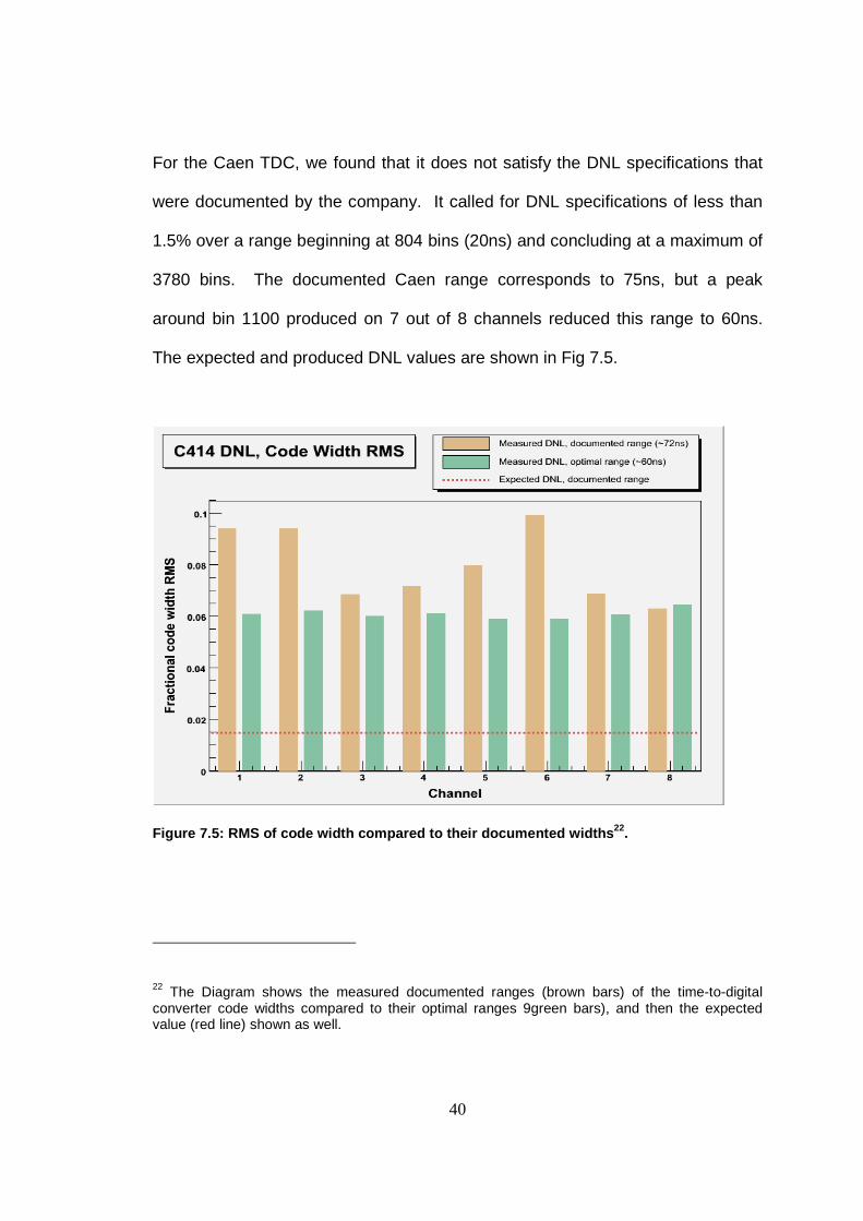
For the Caen TDC, we found that it does not satisfy the DNL specifications that
were documented by the company. It called for DNL specifications of less than
1.5% over a range beginning at 804 bins (20ns) and concluding at a maximum of
3780 bins. The documented Caen range corresponds to 75ns, but a peak
around bin 1100 produced on 7 out of 8 channels reduced this range to 60ns.
The expected and produced DNL values are shown in Fig 7.5.
Figure 7.5: RMS of code width compared to their documented widths22.
22 The Diagram shows the measured documented ranges (brown bars) of the time-to-digital converter code widths compared to their optimal ranges 9green bars), and then the expected value (red line) shown as well.

41
Compared to the C414 TDC, the PH7186 has more consistent DNL over the full
range, so the following table only includes additional ranges when the code width
deviations are greatest near the beginning or end of the full range. Phillips
Scientific's DNL metric, maximum deviation with respect to full range, has also
been added for comparison to the company's document DNL specification, which
claims a DNL of less than .015%.

42
CHAPTER 8: Time Resolution Tests
In high energy physics experiments, particle identification is accomplished
through time-of-flight (TOF) measurements. The TOF system contains two
important factors significant to its performance, the timing resolution and the
efficiency of registering a good event. The overall goal for the existing forward
TOF detector at CLAS is to improve the timing resolution. The current time
resolution gives σ= 120 ps, and the upgrade calls for a resolution achievement of
σ = 60ps.
Such an improvement of the resolution would allow the separation of pions from
kaons up to a momentum of 3 GeV/c and pions from protons up to 6 GeV/c in
momentum.

43
Figure 8.1: Time Difference versus Momentum of particles23. From Fig. 8.1, we can see that these particle separations assume a time
difference of 4σ between the two particles. Thus, allowing a signal with ten
times higher rates to be identified in the presence of other particles.
Previous prototypes using scintillation counters 200cm in length have produced
resolutions of 70ps and 50ps. The 70ps resolution was accomplished using a
single plane of scintillators, while the 50ps measurement was achieved by
utilizing two scintillator planes Smith E., 1999 [6].
23 The Diagram shows the time difference versus the momentum of pion with kaon (red curve) and proton (blue curve). Also for proton and Kaon (green curve). Plot indicates the separation energies that can be achieved.
TTii mm
ee DD
ii ffff ee
rr eenn
cc ee
MMoommeennttuumm ((GGeeVV//cc))
KK-- pp--KK
pp--
44
Both measurements were performed with fast scintillation and XP2020 PMTs.
These resolution values are very encouraging to the upgrade goal of CLAS, the
new design for the forward detector will leave the existing scintillation detectors in
place and simply add an additional layer in front of it. This design should help to
produce an overall resolution of 60ps utilizing two scintillation planes. Therefore,
to ensure an adequate prototype resolution we tested different methods in search
of the best resolution values achievable.
In TOF systems, there are three separate methods one can perform to test the
time resolution of the system. These are the three identical counter method,
reference counter method, and the source method.
8.1) THREE COUNTER METHOD
The commonly used method of measuring time resolution is the three scintillation
counter method. This method is based upon precisely measuring cosmic ray
particles’ time-of-flight. The setup incorporates three identical counters
equidistant of one another.

45
Figure 8.2: Schematic of 3 Counter Method24.
The instant light flashes, the time follows the relation in Fig. 8.2
where ti = 1,…,6 are the corresponding values from the TDC readout. It must
also be taken into account that the tu,m,d values are expected to be independent
upon the scintillator coordinates.
The procedure follows as cosmic particles of constant velocity (speed of light)
strike the three counters which are equidistant and parallel to one another. From
this interaction eq (2) is derived, that is independent of the position and angle.
24 Schematic shows the 3 Counter Method setup with three identical counters with photomultiplier tubes attached, then the signal following the electronic chain to the analog-to-digital converter and time-to-digital converter.
(1)

46
This time parameter is smeared around zero due to the fact that the actual
values are smeared by the time resolution. Thus, the method is based on the
statistical analysis of eq. (2) residuals. Therefore,
And
where i = 1,…,6 assuming all PMTs have timing properties that are the same.
Thus, σPMT must be times the standard deviation measured CHEN E., 2003
[2].
This method is the typical one performed in time resolution and one we will
ultimately utilize. However to cover all possible avenues of timing
measurements, we performed tests using two other methods to gauge how good
our results would be from non-standard means. Keep in mind the measurements
have not been done to date in our prototype measurements. The intent of this
section is simply to apprise you of the normal means utilized. Seemingly, there
are no results to be shown but the overall concept of the method is understood.
(2)
(3)
(4)

47
8.2) REFERENCE COUNTERS METHOD
This method involves three scintillators where two are thin counters and one is a
long extended counter. The two short counters are used as reference counters
and the longer counter is the actual test counter. The time resolution is
measured by using cosmic rays passing through all three counters. All counters
have PMTs on each end and are positioned so that the test counter is in the
middle of the reference counters.
Figure 8.3: Reference Counter Method Image25. 25 Image shows the experimental setup of the Reference Counter Method, where we have to short counters for reference and the long test counter in the middle.
Cosmic Rays

48
The cosmic ray events are selected by the coincidence of the reference counters.
Meaning, once an event in both counters coincide with one another, a good
event signal is registered. The coincidence trigger pulse defines the TDC start
time and generates an ADC gate.
The reference counters which are positioned next to the test counter provide a
timed measurement of the cosmic ray passing through the test counter. This
time is recorded for each event and this procedure is repeated for the desired
amount of events.
The time measurement of the PMT must be time walk corrected, which simply
accounts for the varying time needed for the pulse to exceed the discriminator
threshold. The equation for the time walk is given in Eq. (5), where Ti is the
measured time of the TDC and Qi the ADC count with the subtracted pedestal.
The position dependent time distribution is defined for the left and tight PMTs as:
where ceff is the effective propagation speed of light on the test counter. The
constants ai, and bi, are found by minimizing the widths of the distributions. Both
TL(z) and TR(z) contain the reference counters time distributions defined as:
(5)
(6)
(7)

49
Once we have the time distributions plotted from the recorded data, we fit these
distributions to obtain the overall time resolution (σL, σR) for the left and right side
of the test counter. These resolution values eqs. (9) and (10) are then utilized to
gain the specific widths to calculate the total time resolution of the system.
And from these equations, the weighted average of the system time is given by:
To gain the time resolution of the test counter, the reference counter contribution
must be subtracted in quadrature giving a resolution equation of:
This method helped in covering a possible avenue to time resolution
measurements other than the standard method, but it proved to be unproductive
by taking an excessive amount of time to produce events during testing. The
event rate was of the order of 1 event per 10 minutes.
(8)
(9)
(10)
(11)
(12)

50
Figure 8.4: LED and CFD results of Reference Method26.
This difference of the left and right times was taken and fit to extract the channel
width. Then an overall σ = 390ps was calculated.
8.3) SOURCE METHOD
This method of measuring time resolution was adopted from Kyungpook National
University [1], where they referred to it as the “coordinate method”. It was
26 The histograms show the time width distributions from the reference method for a LED being utilized and then for a CFD.

51
deemed this way simply because it takes into account the relation between
coordinate x of the light flash and the signal arrival times for the left and right
PMTs. This method we followed for our measurements, but will refer to it as the
“source method” in that we only needed a scintillation bar and a radioactive
source to complete all measurements.
Our setup consists of a scintillation bar of 213cm in length with EMI 9954B05
PMTs on both ends. From the PMT, the dynode signal is sent for an ADC gate,
while the anode gives the TDC start signal. The anode signal passed through
the electronic chain that required a high threshold and low threshold, but triggers
an event on the high threshold and provides the timing on the low threshold. The
high threshold is set to 700mV while the low is set to 200mV. Each threshold
required a coincidence between right and left signals before a good event will be
registered. Fig. 8.5 shows the schematic of the setup diagram.

52
Figure 8.5: Schematic of Source Method27.
The digitized value of the TDC was given by
27 The Diagram shows the Source Method where a high threshold is demanded and the low threshold is triggered on. A coincidence between the left/right high thresholds and left/right low thresholds were required for a good event pulse.
(13)

53
where x is the coordinate of the light flash in, tl is left PMT time, and tr is the right
PMT time. The standard deviation of tx relates to right and left PMT resolutions
by
where are the standard deviation times for both PMTs, is
the intrinsic resolution of the TDC, and gives the size of the radiation
source. The intrinsic resolution of the TDC was gathered during the TDC
calibration and differential non-linearity tests. The Phillips TDC module used
gave an intrinsic resolution range from 24ps to 26ps, depending on which input
channel of the module that was used. To get the size of the source, the ionizing
source had to be stepped across a PMT in 1mm steps using a lead window. We
cut a small strip in the lead, to create a window where we moved the source in
1mm increments over the edge of the lead window. With this setup, the lead
should restrict the source to zero count rate until it reaches the edge of the
opening. Thus the rates in the open window should be higher than at the edges,
and from the given count rate distribution we can obtain the size of the source.
Fig. 8.6 displays the experimental setup and shows the distribution of count rate
in millimeter steps.
(14)

54
Figure 8.6: Beam spot setup and fitted distribution28.
An ionization with a known coordinate can be provided by β-particles from the
localized radioactive source. Seemingly, the single PMT resolution can be
determined as
28 The first image shows the experimental setup used to carryout the source size measurement, where you see a lead sheet with a small window cut into it over the surface of a PMT. The histogram shows the distribution from taking 1mm steps across the lead window and fitting the distribution to gain the size of the source.

55
The first time resolution results gave σ = 650 ps.
Figure 8.7: First time resolution results29.
This was simply triggering on low threshold without the demand of high as well,
and without any time-walk corrections applied to the collected data. The next
measurements were performed by demanding high threshold but measuring the
low to produce a better resolution. Fig. 8.7 shows our fitted results were the
resolution improved to σ = 510 ps.
29 The histogram shows the left TDC value used for timing, the right TDC value for the distribution over the bar, and the difference between left and right TDC values with a fit to find the width to calculate the time resolution.
(15)

56
Figure 8.8: The second time resolution results30.
To correct the time-walk introduced by the leading edge discriminators, we
measure the ADC amplitude and the offset to be utilized in the correction
equation. The ADC offset is accomplished by generating a random event that
periodically trigger a read out. This offset is utilized in the correction equation,
where it is subtracted from the ADC value.
The time walk contains a coefficient that is a fitted parameter given by Fig. 8.9.
In this plot we look for the lowest value of sigma to find the best parameter to be
used in the time-walk correction. 30 The histogram shows the left TDC value used for timing, the right TDC value for the distribution over the bar, and the difference between left and right TDC values with a fit to find the width to calculate the time resolution. This time the concept of demanding a high threshold while triggering on the low threshold was used.

57
Figure 8.9: Time Walk Correction Parameterization31
From the plot, we find that the best (lowest) sigma produced is around 14. Once
time-walk was applied, our new time resolution yielded σ = 470 ps.
Figure 8.10: Best time resolution result32
31 The histogram shows the fitted widths for left TDC with time walk correction plotted against those of the right TDC with time walk corrections. The plot shows us our best possible resolution widths with time walk correction. 32 The plot shows the best time difference plot with time walk corrections.

58
CONCLUSION
The TOF upgrade at 12GeV, looks to extend the particle identification to
higher momenta, better charged particle traveling time resolution, and improved
two pion separation. It is our conclusion that with adequate electronic modules
and optimized detector components such as PMTs and magnetic shielding, we
will as optimized tools reach a time resolution of great improvement. With these
three different methods, we are confident to produce the needed detectors with
time resolutions that will definitely improve the existing CLAS time of flight
resolution. We are still too early in our measurements to gauge the success of
whether we will meet the overall resolution improvement by a factor of two. From
the methods discussed in this thesis, we can conclude that the reference counter
method is one that is not suitable to perform detector test series. The biggest
problem that arises in this method is that it takes too great of time to produce an
event using this method. Our best event time production for the reference
method was about 10 to 15 minutes per event. The source method was by far
the easiest method to carry out measurements. It did not provide the best
expected results but will provide a prevalent comparison to the 3 counter method
when it is performed.

59
One reason that the reference method produced a better resolution than the
source method, is that it receives an energy deposit of around 10 MeV. The
source method in comparison obtains about 1 MeV of deposited energy which
means a greater number of photoelectrons cascade within the PMT for signal
production. Another problem to resolve that leads for both methods to lower
resolution results would be the overall concurrent condition of the scintillators,
light guides and PMTs. The scintillator bar that we used was previously
constructed at Jefferson Lab and had several defects, such as improper gluing,
insufficient wrapping, defective phototubes, and misalignment of the light guide to
scintillation. All these parameters will have to be optimized to for an improved
study of the time resolution.

60
LIST OF REFERENCES
[1] Batourine, V. N., Kim W., Nekrasov D. M., Park K., Shin B., Smith E. S., and
Stepanyan S. S., “Measurements of PMT time resolution at Kungpook
National University”, CLAS-NOTE, 2004-016, May 2004.
[2] Chen E., Saulnier M., Sun W., and Yamamoto H., “Tests of a High Resolution
Time of Flight System Based on Long and Narrow Scintillator”, Volume 1, 6,
2967-2974, August 2003.
[3] Eichholz G. G., Poston J. W., “Principles of Nuclear Radiation Detection”, Ann
Arbor Science Publishers, Ann Arbor, 1979.
[4] Grupen C., “Particle Detectors”, Cambridge University Press, New York,
1996.
[5] Knoll, G. F., “Radiation Detection and Measurement”, John Wiley & Sons,
Inc., 1979.
[6] Smith, E. S., Carstens, T., “The time-of-flight system for CLAS”, NIM. A 432,
265–298, 1999.
[7] Abbott, D., Avakian, H., et.al. “The Hall B 12 GeV Upgrade”. 112, 227–237,
2002.
[8] Photomultiplier Tubes Catalog. “Photonis Imaging Sensors”. A-5,2004.


![Present and Future Computing Requirements for Jlab@12GeV Physics Experiments ]](https://static.fdocuments.net/doc/165x107/56813d45550346895da70475/present-and-future-computing-requirements-for-jlab12gev-physics-experiments-568dd84e0963e.jpg)