The Specification, Design, and Implementation of a Home...
25
The Specification, Design, and Implementation of a Home Automation System Javier Castro and James Psota {javy,psota}@mit.edu 6.111: Introductory Digital Systems Laboratory Final Project Massachusetts Institute of Technology This paper presents the specification, design, and implementation of a home automation system that was designed and built as a final project for 6.111 at M.I.T. This system was designed to be flexible and generally programmable, extensible such that adding additional features is relatively simple, and modular and forward-compatible, so that new components can be added without redesigning the entire system. To achieve these goals, the system runs a user-defined program on a special-purpose processor, using real-world sensor inputs as operands. The sensors and other input mechanisms along with user-programmable event schedules allow the user to adjust and customize the home environment. Using sensors that measure temperature, light level, and infrared commands from a remote control, this system will create a comfortable and safe home atmosphere. Design decisions, implementation details, and testing procedures are thoroughly discussed, and the resulting functional system is described.
Transcript of The Specification, Design, and Implementation of a Home...

The Specification, Design, and Implementation of a
Home Automation System
Javier Castro and James Psotajavy,[email protected]: Introductory Digital Systems Laboratory Final ProjectMassachusetts Institute of Technology
This paper presents the specification, design, and implementation of a home automation system
that was designed and built as a final project for 6.111 at M.I.T. This system was designed to be
flexible and generally programmable, extensible such that adding additional features is relatively
simple, and modular and forward-compatible, so that new components can be added without
redesigning the entire system. To achieve these goals, the system runs a user-defined program
on a special-purpose processor, using real-world sensor inputs as operands. The sensors and
other input mechanisms along with user-programmable event schedules allow the user to adjust
and customize the home environment. Using sensors that measure temperature, light level, and
infrared commands from a remote control, this system will create a comfortable and safe home
atmosphere. Design decisions, implementation details, and testing procedures are thoroughly
discussed, and the resulting functional system is described.
2 ·
Contents
1 Introduction 4
2 Design and Implementation 42.1 Input/Sensor Layer . . . . . . . . . . . . . . . . . . . . . . . . . . . . . 4
2.1.1 IR Module . . . . . . . . . . . . . . . . . . . . . . . . . . . . . 42.1.2 Clock Module . . . . . . . . . . . . . . . . . . . . . . . . . . . 92.1.3 Temperature Module . . . . . . . . . . . . . . . . . . . . . . . . 92.1.4 Light Module . . . . . . . . . . . . . . . . . . . . . . . . . . . . 13
2.2 Control Layer . . . . . . . . . . . . . . . . . . . . . . . . . . . . . . . . 142.2.1 Major FSM . . . . . . . . . . . . . . . . . . . . . . . . . . . . . 152.2.2 Instruction Format . . . . . . . . . . . . . . . . . . . . . . . . . 162.2.3 Program Format . . . . . . . . . . . . . . . . . . . . . . . . . . 172.2.4 Compiler . . . . . . . . . . . . . . . . . . . . . . . . . . . . . . 182.2.5 Truth Engine Processor . . . . . . . . . . . . . . . . . . . . . . . 182.2.6 Status Monitor: Hardware . . . . . . . . . . . . . . . . . . . . . 192.2.7 Status Monitor: Software . . . . . . . . . . . . . . . . . . . . . . 20
2.3 Actuator Layer . . . . . . . . . . . . . . . . . . . . . . . . . . . . . . . 21
3 Testing 223.1 IR Module . . . . . . . . . . . . . . . . . . . . . . . . . . . . . . . . . . 223.2 Temperature Module . . . . . . . . . . . . . . . . . . . . . . . . . . . . 223.3 Light Module . . . . . . . . . . . . . . . . . . . . . . . . . . . . . . . . 233.4 Control Layer . . . . . . . . . . . . . . . . . . . . . . . . . . . . . . . . 233.5 Actuator Layer . . . . . . . . . . . . . . . . . . . . . . . . . . . . . . . 233.6 Integration Testing . . . . . . . . . . . . . . . . . . . . . . . . . . . . . 24
4 Conclusion 24
List of Figures
1 Three-layer System Architecture . . . . . . . . . . . . . . . . . . . . . . 52 IR Transmitter/Receiver Waveforms . . . . . . . . . . . . . . . . . . . . 53 Phillips RC-5 Encoding Protocol . . . . . . . . . . . . . . . . . . . . . . 64 IR Module Block Diagram . . . . . . . . . . . . . . . . . . . . . . . . . 75 IR Module State Transition Diagram . . . . . . . . . . . . . . . . . . . . 86 IR Module Simulation Waveform . . . . . . . . . . . . . . . . . . . . . . 87 Clock Module Block Diagram . . . . . . . . . . . . . . . . . . . . . . . 98 Clock Module Waveform Simulation . . . . . . . . . . . . . . . . . . . . 109 Temperature Module Block Diagram . . . . . . . . . . . . . . . . . . . . 1110 A/D Interface State Transition Diagram . . . . . . . . . . . . . . . . . . 1211 Sensor Module State Transition Diagram . . . . . . . . . . . . . . . . . . 1312 Temperature Module Simulation Waveform . . . . . . . . . . . . . . . . 1313 Light Module Simulation Waveform . . . . . . . . . . . . . . . . . . . . 1414 Simple Thermostat Program . . . . . . . . . . . . . . . . . . . . . . . . 1415 Top-Level Control Unit Block Diagram . . . . . . . . . . . . . . . . . . 1516 Control Unit Major FSM . . . . . . . . . . . . . . . . . . . . . . . . . . 16

· 3
17 64-bit Instruction Format . . . . . . . . . . . . . . . . . . . . . . . . . . 1618 Compiler Interface . . . . . . . . . . . . . . . . . . . . . . . . . . . . . 1819 Truth Engine Processor Block Diagram . . . . . . . . . . . . . . . . . . 1920 Status Monitor FSM . . . . . . . . . . . . . . . . . . . . . . . . . . . . 2021 Status Monitor Screen Shot . . . . . . . . . . . . . . . . . . . . . . . . . 2122 Lab Kit Integration Testing Setup . . . . . . . . . . . . . . . . . . . . . . 24
List of Tables
I Opcode Map . . . . . . . . . . . . . . . . . . . . . . . . . . . . . . . . . 17
4 ·
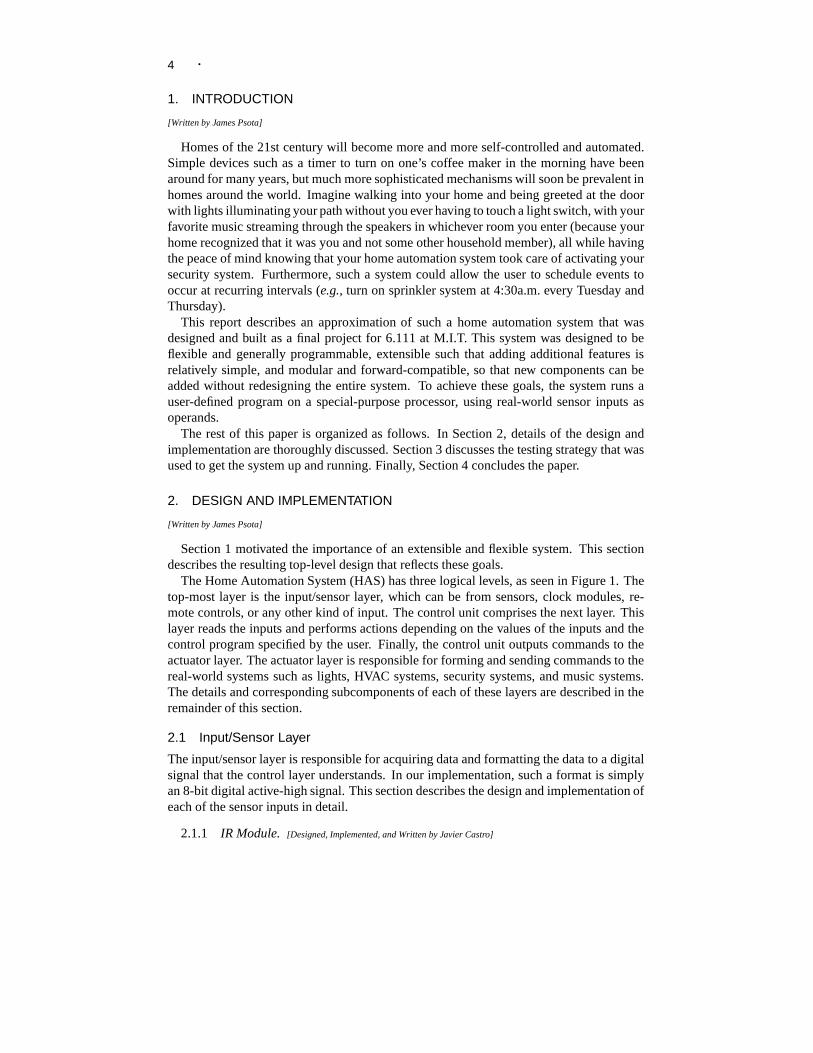
1. INTRODUCTION
[Written by James Psota]
Homes of the 21st century will become more and more self-controlled and automated.Simple devices such as a timer to turn on one’s coffee maker in the morning have beenaround for many years, but much more sophisticated mechanisms will soon be prevalent inhomes around the world. Imagine walking into your home and being greeted at the doorwith lights illuminating your path without you ever having to touch a light switch, with yourfavorite music streaming through the speakers in whichever room you enter (because yourhome recognized that it was you and not some other household member), all while havingthe peace of mind knowing that your home automation system took care of activating yoursecurity system. Furthermore, such a system could allow the user to schedule events tooccur at recurring intervals (e.g., turn on sprinkler system at 4:30a.m. every Tuesday andThursday).
This report describes an approximation of such a home automation system that wasdesigned and built as a final project for 6.111 at M.I.T. This system was designed to beflexible and generally programmable, extensible such that adding additional features isrelatively simple, and modular and forward-compatible, so that new components can beadded without redesigning the entire system. To achieve these goals, the system runs auser-defined program on a special-purpose processor, using real-world sensor inputs asoperands.
The rest of this paper is organized as follows. In Section 2, details of the design andimplementation are thoroughly discussed. Section 3 discusses the testing strategy that wasused to get the system up and running. Finally, Section 4 concludes the paper.
2. DESIGN AND IMPLEMENTATION
[Written by James Psota]
Section 1 motivated the importance of an extensible and flexible system. This sectiondescribes the resulting top-level design that reflects these goals.
The Home Automation System (HAS) has three logical levels, as seen in Figure 1. Thetop-most layer is the input/sensor layer, which can be from sensors, clock modules, re-mote controls, or any other kind of input. The control unit comprises the next layer. Thislayer reads the inputs and performs actions depending on the values of the inputs and thecontrol program specified by the user. Finally, the control unit outputs commands to theactuator layer. The actuator layer is responsible for forming and sending commands to thereal-world systems such as lights, HVAC systems, security systems, and music systems.The details and corresponding subcomponents of each of these layers are described in theremainder of this section.
2.1 Input/Sensor Layer
The input/sensor layer is responsible for acquiring data and formatting the data to a digitalsignal that the control layer understands. In our implementation, such a format is simplyan 8-bit digital active-high signal. This section describes the design and implementation ofeach of the sensor inputs in detail.
2.1.1 IR Module. [Designed, Implemented, and Written by Javier Castro]

· 5
control
sensors/
inputs
actuators
templight
levelclock
remote
control
commands
special-
purpose
processor
status
Fig. 1. Three-layer System Architecture
A remote control interface is provided as an input that can be used to interact withthe HAS. In order to make this possible, the system interfaces with an infrared receiverwhich demodulates a 36kHz infrared signal to a digital format that can then be decodedand offered as input to the HAS control layer . The basics of infrared transmission arethat when an infrared light is turned on and off at a frequency of 36kHz, the signal isinterpreted to be in the on state (See Figure 2). When no light is flashing, the signal is inthe off state. There are many different methods that can be used to encode a signal usinginfrared transmission. The Phillips RC-5 protocol was chosen for the HAS because it iswell documented and has a fairly simple protocol.
Transmitter
Receiver
Transmitter
Receiver
Fig. 2. IR Transmitter/Receiver Waveforms
Rather than using a variable bit-length encoding scheme, as is used by other protocols,the RC-5 protocol uses a form of Manchester Encoding to represent 1’s and 0’s. Thismeans that in order to transmit a 1, the transmitter is silent for the first half of a bit, andblinking at 36kHz for the second half of the bit. A 0 is transmitted by a similar sequence:an on signal followed by an off signal.
Every message in the RC-5 protocol is 14 bits in length and is repeated every 114ms aslong as a key is pressed. Each bit is 1.8ms in length meaning that each half bit is 0.9mslong. A message takes 25.2ms to transmit and is repeated every 114ms while a button ispressed. Repetition occurs in case the signal was not received correctly the first time. Eachmessage takes the form that is shown in Figure 3. The first two bits are called the startbits and are always 1’s. The next bit is called the check bit and is used to signal when anew button has been pressed. The check bit is in one state as long as a button is pressed sothat an IR receiver can determine whether a message is new or a repetition of the previous

6 ·
chk
1 1 1 1 1 10 0 0 0 0 0 0 0
start address commandchk
1 1 1 1 1 10 0 0 0 0 0 0 0
start address command
Fig. 3. Phillips RC-5 Encoding Protocol
message. This allows users some room for error. For example, if a person holds down the“7” button on a remote control for longer than 114ms, the receiving system will understandthat only a “7” was intended and that “77” is not an intended input. The next button presswill toggle the state of the check bit. This change in bit is to be expected by the receivingsystem and indicates that a new button has been pressed. After the check bit, five addressbits are transmitted. These bits are used to tell a system that the message is directed to it.For example, address 0 is reserved for TV1 and address 1 is reserved for TV2. This meansthat people can have two TV’s in the same room, and commands intended for one TV arenot processed by the other. The last six bits of the message are the command bits. Thesebits specify which button has been pressed. A television, for example, could then turn itsmonitor on or change channels. The Home Automation System checks the address bits ofa message only to ensure that a message is still being transmitted. This means that it doesnot matter what the address bits actually are, just that they abide by the RC-5 protocol inthat the state of the first half of a bit is different from the state of the second half of the bit.
Responsible for receiving the infrared signal from a remote control is a TSOP2236 chipfrom Vishay electronics. The circuit is intended to detect a 36kHz infrared signal andinterpret it as a valid 1. The TSOP2236 actually inverts the signal that is received so that avalid 1 corresponds to the low state and a valid 0 corresponds to the high state. Followingthe instructions found on the data sheet, a 4.7µF capacitor was placed between the powerand ground leads and a 100Ω resistor was placed between the power lead and Vdd. Thepurpose of the capacitor and resistor is to suppress power supply disturbances (Please referto Figure 4).
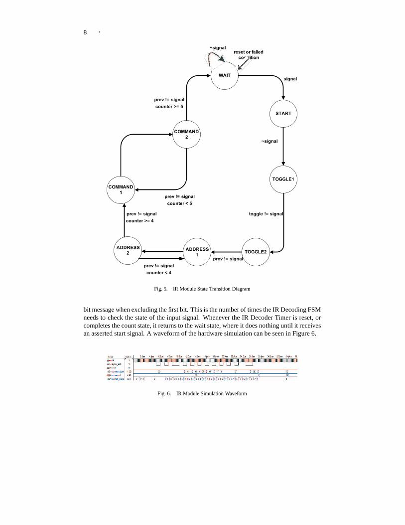
The IR Decoding FSM is responsible for taking the demodulated signal from the IRreceiver and parsing it for the command bits (See Figure 5). If the signal that is beingreceived does not follow the RC-5 protocol, the FSM resets and waits for the next signal.A negative edge in the input signal asserts the start signal output of the FSM. Every pos-itive clock edge signals the IR Decoding FSM to check whether the read signal which isprovided by the timer is asserted. If the read signal is asserted, the module will check tosee if it needs to change state; otherwise no state change will occur.
The FSM begins in the wait state. Since the read signal will only be asserted if themodule has already received a negative edge as input from the IR receiver, the wait statechecks to see that the second start bit is being received at this point. If the input signal islow, the FSM moves to the start state, otherwise the timer is reset and the FSM remains inthe wait state. If in any of the states, the RC-5 protocol is broken, the FSM resets the timerand returns to the wait state. The start state checks that the input signal is high (second halfof the second start bit) when the read signal is asserted and proceeds to the toggle1 state. Inthe toggle1 state, the FSM checks that the current message that is being received is not the

· 7
Data_en
12
Register Data
IR Receiver
Synchro
niz
er
FSM
Timer
Registers
2 Start, ResetRead
Reg_en
Sig
nal
Sig
nal_
sync
12
Data_en
12
Register Data
IR Receiver
Synchro
niz
er
FSM
Timer
Registers
2 Start, ResetRead
Reg_en
Sig
nal
Sig
nal_
sync
12
Fig. 4. IR Module Block Diagram
same as the previous message that was received. If the current message is a new message,the state of the input signal is saved to two registers. One is for reference on the next FSMiteration. The other register is the generic prev register where the state of the first half ofeach bit is stored. The FSM now proceeds to the toggle2 state. If the state of the inputsignal, at this point is different from the value held in the prev register, the FSM proceedsto the address1 state. On assertion of the read signal, the FSM will store the state of theinput signal to the prev register, and move to the address2 state. While in the address2state, if the state of the input signal is different from the value held in the prev registerthe FSM will assert the data en signal so that the address bit that is being provided as aninput signal can be stored if desired. If five address bits have been received, the FSM nowmoves to the command1 state; otherwise it returns to the address1 state and repeats theprocess described above. The two command states (command1 and command2) behavethe same way as the two address states, except that on the last command bit, the reg intsignal is asserted. The reg int signal is used to enable a register which will hold the parsedcommand bits. The reg en signal gets the value of reg int one clock cycle later so that allof the command bits can be registered in the series of registers before being placed in a 6bit register all together.
The decoder timer module has a start and reset signal as controls and a read signal asoutput. The timer module is a small state machine that waits for a start signal. Once thestart signal is asserted, it proceeds to a delay state where it counts the length of a quarter bit(.45ms). Once this delay has occurred the timer moves to the count state where the timercounts .9ms and then asserts the read signal for the length of the period of the system clock(10MHz is expected). This sequence is repeated 26 times: the number of half bits in the 14
8 ·
WAIT
TOGGLE1
START
COMMAND
2
~signal
signal
reset or failed
condition
TOGGLE2ADDRESS
1
COMMAND
1
ADDRESS
2
toggle != signal
~signal
prev != signal
prev != signal
counter < 4
prev != signal
counter >= 4
prev != signal
counter < 5
prev != signal
counter >= 5
Fig. 5. IR Module State Transition Diagram
bit message when excluding the first bit. This is the number of times the IR Decoding FSMneeds to check the state of the input signal. Whenever the IR Decoder Timer is reset, orcompletes the count state, it returns to the wait state, where it does nothing until it receivesan asserted start signal. A waveform of the hardware simulation can be seen in Figure 6.
Fig. 6. IR Module Simulation Waveform

· 9
2.1.2 Clock Module. [Designed, Implemented, and Written by James Psota]
One of the goals of the HAS was to be able to schedule actions and events for certaintimes during the day or days of the week, for instance. Because of the HAS’s flexibledesign, incorporating such functionality was simply a matter of adding another set of inputsthat provided the current time and date.
The clock module keeps track of the following fields of the current date:
—seconds
—minutes
—hours
—day of week
—date
—month
—year
The system takes into account the number of days in each month, as well as leap years.The block diagram of the system is shown in Figure 7. Note the interdependence of eachsub-unit on one another. There are some obvious unidirectional dependencies, such as thatfrom the minute counter to the second counter. One of the dependencies, however, is bi-directional; the dependency between the date counter and the month counter is two-way,as the date counter must be aware of which month it is to determine when to rollover, andthe month counter must know when to increment to the next month.
10 MHzsec min hour day
date
month year6 6 5 3
5 3 8
Fig. 7. Clock Module Block Diagram
Figure 8 shows a simulation of the clock module. Note that the date in the simulationis initialized at February 28, 2004 23:59:45, and that the date transitions to the 29th ofFebruary, as 2004 is a leap year.
2.1.3 Temperature Module. [Designed, Implemented, and Written by Javier Castro]
The Temperature Module is responsible for providing the control layer with a repre-sentation of the ambient temperature. The module takes a voltage, which represents theambient temperature, as input and converts the information to a 2’s complement binarynumber which represents the temperature in degrees Fahrenheit (See Figure 9). The factthat the temperature is initially represented as a voltage and then converted to a binary

10 ·
Fig. 8. Clock Module Waveform Simulation
number implies that there is an analog as well as a digital component to this module. Theanalog component provides a voltage to an AD670 analog to digital (A/D) converter. TheAD670 is controlled by a finite state machine which is located within the FPGA. There isa Sensor FSM which controls the A/D Interface FSM, and is triggered by a sample timer.When the sample signal is asserted by the Timer module, the previously converted Fahren-heit temperature and the previously computed binary voltage value are registered and anew A/D conversion is started.
The analog part of the temperature module consists of a thermistor, 62kΩ resistor, andan LM741 Op Amp. A thermistor is a component that has a variable resistance whichdepends on the ambient temperature. It is made of D14.0 material and has a resistanceof 100kΩ at 25oC. A voltage divider was created by placing the thermistor in series withthe 62kΩ resistor and measuring the voltage across the non-variable resistor. The range ofvalid temperatures to 50-95oF, which in turn restricted the resistance of the thermistor toa range from 61kΩ to approximately 222kΩ. The reason for choosing a 62kΩ resistor forthe voltage divider was so that the range of input voltages to the A/D converter would fallinto the range of 0-2.55V. Due to a 10kΩ load resistance located in the AD670, the voltagefrom the voltage divider had to be passed through an operational amplifier which wasarranged in a voltage follower configuration. This caused the voltage, which the AD670was experiencing across its leads, to be the voltage that was expected from the calculationsof the voltage divider.
The A/D Interface FSM allows the temperature module to obtain a binary representationof the temperature dependent voltage from an AD670 which is setup so that the outputis formatted in straight binary representation and the input that is expected is from 0V to2.55V. Please refer to Figure 10 for a state transition diagram. The A/D Interface has ago and status signal as inputs, and outputs a busy signal, a reg en signal, and three controlsignals (cs bar, ce bar, and r w bar). The go signal is connected to a sensor FSM and isasserted whenever an A/D conversion and reading should take place. This submodule hasnine states: an idle state, four
read states, three conversion states, and a wait state. The idle state is the initial as well asreset state of the FSM. This state waits for the go signal to be asserted in order to proceedto the next state; otherwise nothing occurs in this state. There are four read states so thatthe setup and hold time requirements for the read cycle of the AD670 are met. The busysignal is asserted during the four read states, and the reg en signal is asserted during onlythe fourth read state. In order for the AD670 to begin reading the data, the cs bar andce bar signals must be held low and the r w bar signal must be high for at least 250ns.As a result, there must be three read states, with the fourth allowing for pin stabilizationand registering of the value which is being read. The reg en signal is used to enable aregister which holds the binary representation of the newest voltage sample. The A/D

· 11
AD
67
0
A/D Interface
Syn
ch
ron
ize
r
Co
nve
rsio
n
Mo
du
le
Te
mp
era
ture
Re
gis
ter
Volta
ge
Re
gis
ter
Sensor FSM
Timer
3 ~cs, ~ce, r/~w
8
voltage
8 8
reg_en
sta
tus
busy go
sample
8
sensor_en
analog_in
Fig. 9. Temperature Module Block Diagram
Interface FSM then continues to the three conversion states. Again, these states satisfythe setup time requirement for the write cycle of the AD670. The final wait state of thisFSM is provided so that the cs bar, ce bar, and r w bar signals remain low until the AD670actually begins a new write cycle. The wait state is waiting for the status signal from theAD670 to be asserted before returning the FSM to the idle state.
The Sensor FSM is responsible for registering the newest voltage to Fahrenheit conver-sion as well as starting a new A/D conversion whenever a sample is desired. The SensorFSM has five states (See Figure 11). The idle state is where the Sensor FSM waits for thenext sample time. Once the sample signal is asserted, the FSM proceeds to the registerdata state where it enables the sensor register so that the previous Temperature calculationis available for the control layer to read. The next three states concern A/D conversion andare provided so that the Sensor FSM will not return to the idle state until an A/D conversionhas been initiated. The start reading state sends a start signal to the A/D Interface FSM.Next, the Sensor FSM waits for the A/D Interface to signal that it is no longer busy before

12 ·
IDLE
READ1
READ0
CONV2
WAIT_STA
TUS_HIGH
~go
go
~status reset
status
READ2READ3
CONV1
CONV0
Fig. 10. A/D Interface State Transition Diagram
returning to the idle state.The voltage which is sampled by the AD670 needs to be converted to a Fahrenheit value
so that the control layer is able to process the data. Using matlab, the voltages whichappear across the voltage divider at different temperatures from the range of 50-95oF werecomputed and converted to binary. Using this information, a look up table, implementedby a Verilog if tree, was generated within a clocked module so that whenever a voltageprovided as input, the module would produce the corresponding temperature, in degreesFahrenheit, as output. The reason for using a look up table, rather than some other method,was because the resistance of the thermistor, which was used in the analog component ofthe temperature module, is non-linear.
The timer block of the Temperature module is a clock divider that takes a 10MHz clocksignal, and slows it down to an arbitrary length periodic signal. For the purposes of theHAS, the timer was set to assert its sample signal once every second. This is becausetemperature is not a rapidly changing environment variable and instead is fairly constantin the home environment. Figure 12 contains an image with a simulation waveform of this

· 13
IDLE
START_RE
ADING
REGISTER
_DATA
WAIT_BUS
Y_HIGH
WAIT_BUS
Y_LOW
~sample
~busy
busy
reset
busy
Fig. 11. Sensor Module State Transition Diagram
module.
Fig. 12. Temperature Module Simulation Waveform
2.1.4 Light Module. [Designed, Implemented, and Written by Javier Castro]
The Light Module was created by placing a PDV-P5001 photoresistor from PhotonicDetectors Inc. in series with a 2kΩ resistor and measuring the voltage across the non-variable resistor. The result is a voltage divider similar to the one used in the TemperatureSensor. Once again, the voltage had to be passed through an LM741 Op Amp in order toavoid the voltage drop across the resistance load of the AD670. The two systems, LightModule and Temperature Module, were similar enough to use all of the same componentswith the exception of a substituted conversion module. The reason for choosing a 2kΩ
resistor as opposed to any other resistance was so that the voltage measured by the AD670would fall into the range of 0-2.55V. At ambient light levels, the voltage across the non-variable resistor is approximately 2.46V.

14 ·
Since light level is measured in lumens, it seemed to make more sense to have a scalefrom 0-9 to represent different levels of light. This is because, unlike temperature, peopledo not have a general idea for how many lumens a particular level of light may be. Withthis in mind, the Light Module takes a voltage that ranges from 0-2.55V that is representedin straight binary returns which decade the voltage falls into with 9 corresponding to 2.46Vand higher, and 0 corresponding to 0.36V and lower. This module was implemented usinga series of if statements. Figure 13 depicts a simulation waveform of this module. Forassociated A/D interface and state transition diagrams, please refer to Figure 10 and 11.The block diagram is similar to that depicted in Figure 9, but has a different conversionmodule.
Fig. 13. Light Module Simulation Waveform
2.2 Control Layer
[Designed, Implemented, and Written by James Psota]
Before diving into the lower-level details of the control system, here is a primitive ex-ample of how the HAS would be used as a thermostat. Assume the system has an inputthat specifies the current temperature in the room that is to be climate-controlled, and hasan actuator output that is connected to a heating unit. Also assume that the user desires toturn the heat on when the temperature falls below 66F, and turn the heater back off whenthe temperature raises above 68F. The user would then have to write a program to specifythese actions, with one instruction to turn the heater on when the “on” condition is true,and one instruction to turn the program off when the “off” condition is true. The specificinstruction format is described in section 2.2.2, but a textual description of each of theinstructions as seen in Figure 14 is illustrative. For this example, assume the temperaturesensor plugged into sensor input slot 7, and the heater is plugged into actuator output slot3.
Instruction-I If sensor 7 < 66, set actuator 3 to 1Instruction-II If sensor 7 > 68, set actuator 3 to 0
Fig. 14. Simple Thermostat Program
This program, when run by the control unit, performs the user’s desired action.The top-level block diagram of the control unit can be seen in Figure 15. The cu control
module is the major FSM that prompts the other components to stop and go. Thetruth engine block is the main processing unit. This block reads instructions from theinstruction memory (implemented in an internal RAM) and executes it using sensor inputs

· 15
as operands. Finally, the status monitor provides the user with a real-time view of thesystem’s inputs and outputs via the RS232 port of a host PC.
...
...
...
cu_control
(major FSM) truth engine
processor
instruction
memory
status
monitor
load_inputs
start_exec
done_pgm
start_status_rpt
done_status_rpt
txd (to PC RS232)
actuator outputs
addr data
inputs/sensors
16 1616
8 8 8
8 8 8
864
...
Fig. 15. Top-Level Control Unit Block Diagram
2.2.1 Major FSM. [Designed, Implemented, and Written by James Psota]
The control unit’s major FSM can be seen in Figure 16. The system completes an entireloop of the control flow about 100 times a second, as dictated by an internal counter. Thesystem waits in the INIT state until the .01 second pulse is asserted. Then, it enters intothe LOAD INPUTS state. This state loads the inputs (e.g., from the sensors) so that theystay constant throughout the entire current run of the program. It’s important that theinputs remain constant throughout the program run for reasons that will be explained inSection 2.2.5. After the inputs are registered, the system enters the EXEC PGM state,which prompts the truth engine to begin processing the program stored in memory. Whenthe program has completed execution, the system transitions into the DONE PGM state.Finally, the system enters the REPORT STATUS state, where it cycles through the inputsand outputs and reports their current state via the RS232 port of a host PC.

16 ·
INIT
EXEC_
PGM
LOAD_
INPUTS
DONE_
PGM
REPORT_
STATUS
~go
go
~done_pgm
~done_status_rpt
reset
Fig. 16. Control Unit Major FSM
2.2.2 Instruction Format. [Designed, Implemented, and Written by James Psota]
The example shown in Figure 14 generally illustrated the types of actions and address-ing the program needed to perform. Recall that the user needed to specify the followinginformation: which operands to use, which operation to perform on the operands, whichoutput value to set, which value to set the output value to. Additionally, the user needs tobe able to specify if the operands inputs or immediates. The resulting 64-bit instructionformat can be seen in Figure 17.
1 4 1 12 1 12 4 16 5 8
op
value1 value2
output
valuenext_pc
cc output s
ignal
(rese
rved)
Fig. 17. 64-bit Instruction Format
The first field is called the cumulative condition field, which specifies if this instructiondepends on the result of one or more previous instructions. This feature was added becauseeach instruction can only specify a single operation, but there are times when the user maywant to execute an action if multiple conditions are true. For instance, the user may want

· 17
to turn on the lights at 18:00 if it’s Friday or Saturday, but not any other day. In this case,the user would specify the two conditions in separate instructions, specify a null actionon the first instruction, and the desired action on the second instruction which has thecumulative condition bit set. This feature substantially increases the scope of the system’sprogrammability.
The next four bits specify the opcode. The available opcodes can be seen in Table I.Note that the truth engine only executes boolean operations.
value operation0 less than1 greater than2 equal3 not equal4 less than or equal5 greater than or equal6 (reserved)7 (reserved)8 (reserved)9 (reserved)10 (reserved)11 (reserved)12 (reserved)13 zero (nop)14 one (always true)15 done pgm
Table I. Opcode Map
The next field specifies the first operand. The first bit specifies if the operand is animmediate, in which case the remaining 12-bit value field is all used as an immediate. Ifthe top bit specifies that this operand is an input, the low four bits of the value field areused as an index into a multiplexor which selects the appropriate input. The next 13 bitsare analogous to the first operand field, but specify the second operand field.
The next four bits specify which output should be asserted. The 16 subsequent bitsspecify the value the output should be set to if the condition is true. 16 bits of output valueprovide a wide range of options for the end user, such as sending IR signals or simplyspecifying a wide range of output values.
Finally, the last used field of the instruction is the next pc field. This field specifies theunconditional address of the instruction that should be executed after this one.
2.2.3 Program Format. [Designed, Implemented, and Written by James Psota]
The program is specified in the instruction memory, which is initialized by a memoryinitialization file. As in any computer system, the truth engine processor expects programsto be in a certain format. The processor will always start by executing the instruction ataddress 0, and unconditionally follow the next pc fields of each instruction. The programterminates when the processor sees a done pgm instruction. Thus, all programs must obeythe following two constraints:

18 ·
(1) The first instruction must exist at PC=0
(2) The last instruction must contain the done pgm instruction (opcode 15)
2.2.4 Compiler. [Designed, Implemented, and Written by James Psota]
The HAS comes with a reasonably user-friendly interface that allows users to createprograms in an intuitive way. The interface, which runs any host PC capable of executinga Perl script, steps the user through a series of simple questions. The user’s input is passedto a compiler which in turn packages up 64-bit instruction words that implement the user’srequest. The resulting output of the program is a memory initialization file that is used toprogram the instruction memory. A screenshot of the compiler can be seen in Figure 18.
Fig. 18. Compiler Interface
2.2.5 Truth Engine Processor. [Designed, Implemented, and Written by James Psota]
The truth engine accounts for a large amount of the control unit’s complexity. As men-tioned above, it has the job of executing the program using sensor inputs as operands, andwriting outputs to the actuator layer. Figure 19 shows the top-level datapath design.
The 64-bit instruction is read in from the instruction memory and placed into a regis-ter. The instruction completely dictates the program’s operation – which operands to use,which operation to execute, which instruction to execute next, etc. The opcode field ispassed into a decode module, which simply reports to the ALU which operation it shouldexecute, and produces the done pgm signal if a done pgm opcode is seen. The value fieldsare used to either select which sensor input to choose, or to specify which value immediateto use. The values are passed to the ALU, which performs the appropriate operation. Theresult of the ALU operation (either a 1 or a 0) is used to enable loading of the appropriateactuator register. The output signal field is fed to a demultiplexor which asserts exactly oneof 16 enable signals. This signal is another one of the few signals used to enable loadingof the actuator registers. The top bit of the instruction along with the alu result is used todetermine the value to write to the cumulative condition register, which keeps track of pre-vious alu results so that multiple condition results are stored. This ultimately implementsthe cumulative condition feature described above, and is used in the enable logic that loadsthe actuator registers.

· 19
decode
...
sensor inputs8 8 8
actuator outputs
16 16 16
...
done_pgmalufn
next_pc
cumulative
condition
register
actuator
select
(sa
me
fo
r se
con
d in
pu
t)
PC INST
...
4
648
1
4
16
4
112
8
12
4
64
8
ALU
[63]
[49..46]
[58]
[57..46]
[7..0]
[62..59]
[28..13]
[32..29]
actuator
registers
actuator
select
output
valuealu_result
sensor A sel
signal1 imm
signal1 sel
Fig. 19. Truth Engine Processor Block Diagram
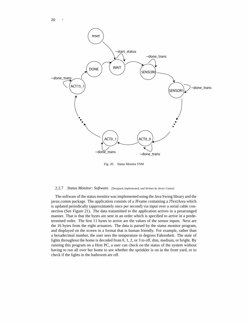
2.2.6 Status Monitor: Hardware. [Designed, Implemented, and Written by James Psota]
The status monitor displays the current values of the system’s inputs and outputs. Thisfeature provides the user with a view of current conditions in the home environment, suchas which lights are on and what the temperature is. It is also a useful tool in helping theuser program and test the system. The system interacts with a host PC to display the status.The FPGA sends the data to the PC via the RS232 serial interface
As can be seen in Figure 16, the status is reported after the program has completedexecution. Note that each sensor input is 1 byte wide, and each actuator output is 2 byteswide. As the serial interface module1 accepts 1 byte of data at a time, the status monitorhas to cycle through the data, sending one byte after another. As can be seen in Figure20, the values of each of the signals are sent first, and the values of the actuators are sentsecond. Note that the actuators’ values are sent in two halves – the low order byte is sentfirst, and the high order byte is sent second.
1provided by HyungBin Son
20 ·
......
reset
WAIT
SENSOR0
SENSOR1
ACT0_0ACT0_1
ACT15_1
DONE
~done_trans
~done_trans
~done_trans~done_trans
~done_trans
~start_status
Fig. 20. Status Monitor FSM
2.2.7 Status Monitor: Software. [Designed, Implemented, and Written by Javier Castro]
The software of the status monitor was implemented using the Java Swing library and thejavax.comm package. The application consists of a JFrame containing a JTextArea whichis updated periodically (approximately once per second) via input over a serial cable con-nection (See Figure 21). The data transmitted to the application arrives in a prearrangedmanner. That is that the bytes are sent in an order which is specified to arrive in a prede-termined order. The first 11 bytes to arrive are the values of the sensor inputs. Next arethe 16 bytes from the eight actuators. The data is parsed by the status monitor program,and displayed on the screen in a format that is human friendly. For example, rather thana hexadecimal number, the user sees the temperature in degrees Fahrenheit. The state oflights throughout the home is decoded from 0, 1, 2, or 3 to off, dim, medium, or bright. Byrunning this program on a Host PC, a user can check on the status of the system withouthaving to run all over her home to see whether the sprinkler is on in the front yard, or tocheck if the lights in the bathroom are off.

· 21
Fig. 21. Status Monitor Screen Shot
2.3 Actuator Layer
[Written by Javier Castro]
In order for the Home Automation System to perform its function and be useful to ahome owner, it needs to interact with real world systems. Examples of such systems arelights, heating and A/C units, and sprinkler systems. A user needs to have the ability totell the HAS that the sprinkler system should be turned on between 5:00am and 6:00amevery Tuesday and Thursday. In order to realize this command, the Home AutomationSystem has actuators which format output from the control layer to a form that householdsystems can understand. If a user of the home automation system has placed the system

22 ·
into vacation mode, and the television is scheduled to turn on at 7:30pm, the control layersimply outputs the 6 bit power signal command to an infrared transmitter module that isconnected to the system. The transmitter module then takes the address, 0x0C, and outputsthe corresponding infrared signal that results in a TV actually turning on.
Due to a pin limitation on the FPGA’s, there is a HAS status monitor, implemented inJava, that runs on a host computer. The state of the HAS’s actuators is transmitted to thehost computer via serial cable connection so that the data may be formatted and displayedon the monitor of the host computer.
3. TESTING
[Written by Javier Castro and James Psota]
Due to the modular nature of the design of the HAS, it was straight forward to test eachmodule individually. In doing so, bugs were easy to spot, locate, and fix. Thorough sim-ulation testing was performed on each module before being programmed onto an FPGA.Then, once the simulations ran according to specification, an FPGA was programmed withthe architecture, and more component testing took place. The biggest problem in testingwas due to faulty HEX displays and burned out pins on the lab kits.
3.1 IR Module
The IR Module had a tricky bug which was hard to locate, due to successful simulations.The module simulated according to what was expected to occur given an input that timedout (did not adhere to RC-5 encoding), and did would successfully read a properly formedsignal. The problem was, that if allowed to start up normally, it would enter a state wherethe internal reset signal to the timer was constantly asserted. This was found by progres-sively showing more and more signals in the simulator, and by starting the input signalwhich was received from the IR receiver a little bit later. The problem was solved by plac-ing a level-to-pulse module before the reset signal to left the IR Decoding FSM so thatthe IR Timer would only receive a pulse, and therefore be allowed to start upon receivinga new start pulse. This solved the grid lock issue. In order to prove that the IR modulewas in fact decoding IR signals, the output from the IR Module was displayed on the HEXdisplays of the FPGA lab kits and simultaneously compared to an oscilloscope reading ofthe pins on the IR module. Since the address bits of the waveforms matched the outputshown on the HEX displays, it was verified that the IR Module performed properly andaccording to its specification.
3.2 Temperature Module
Some experimentation was involved in testing the Temperature Module. In order to en-sure that the thermistor-voltage divider was working properly, the voltage across the non-variable resistor was measured using an oscilloscope. Once it was verified that the voltagewas as expected, the FPGA was programmed with the digital portion of the TemperatureModule. The AD670 was wired up with its controls from the FPGA, appropriate groundand power signals were supplied to its formatting pins, and the voltage from the voltagedivider was fed to the A/D. Being wary of a load resistance across the leads of the AD670,the voltage was, again, measured with an oscilloscope. It was discovered at this point, thatthe load resistance of the AD670 was indeed something to take into consideration as itwas on the same magnitude as the resistor that the voltage was being divided across. After

· 23
much thought, an LM741 Op Amp was placed in a voltage follower configuration, so thatthe voltage of the output would match that of the inputs. This idea worked, and the Op Ampwas included as a permanent part of the Temperature Module. Once this issue had beenaddressed, physical testing of the digital part of the Temperature module was performed.This involved having the FPGA display the output from the Temperature Module on itsHEX displays by assigning the output pins appropriately. Since a sample is taken everysecond, the display was steady and displayed the ambient temperature in hexadecimal. Ifthe thermistor was heated up, the temperature would rise; if it was cooled down, tested bygrounding the V+ lead, the temperature bottomed out to 50oF.
3.3 Light Module
Since most of the Light Module was implemented by reusing parts from the TemperatureModule, most of the testing was completed when the Temperature module was created.All that was left to test, at this point, was that the conversion module performed adequatelyenough, for the purposes of the Truth Engine located in the control layer.
3.4 Control Layer
The control layer was thoroughly tested in simulation incrementally. A small subset of thecontrol system was built first to work out details as the design was being finalized. Forinstance, the initial system only had one sensor input, one actuator output, one opcode, ex-ecuting one instruction. After this minimal system was debugged, more and more featuresand components were added until the final desired system was realized.
After thorough simulation testing, the control layer logic was placed on an FPGA forfield testing. The first test involved the execution of a one-instruction program. The pro-gram would take the data from one sensor as input, and output the appropriate result to theappropriate actuator. Next, more and more instructions were added to the simple programso that the full capabilities of the truth engine could be tested. At this point, actuatorswere asserted or not asserted by turning the LEDs of the FPGA lab kits on or off. Oncea multi-instruction program could be executed, with dependence on several inputs, testingwas complete and ready for integration.
3.5 Actuator Layer
Since the results of the actuator layer are output over a serial cable. By connecting thiscable to a host computer, where a Java program resides, the information being sent overthe cable could be displayed onto the monitor for simple debugging. One of the problemsthat occurred while implementing this process was that the information being sent over theserial cable, whenever the lab kit was initially turned on, was junk. The method discoveredfor initiating the HAS/Host Computer communication was to start up the HAS, place it intothe reset state, and then initiate the program on the Host Computer. At this point, wheneverthe HAS was taken out of the reset state, information would be transmitted in an expectedmanner to the program running on the Host Computer, and as a result, displayed on thecomputer monitor in a decipherable manner. A second problem which was encounter,while interfacing with the Java program, was that the screen was flickering. This was theresult of updating the screen too often. In order to solve this problem, the period at whichdata was sent over the serial cable was slowed down, and the amount of times that theJava program would update the screen was slowed down. After these changes, the monitorwould display new data about once a second.
24 ·
3.6 Integration Testing
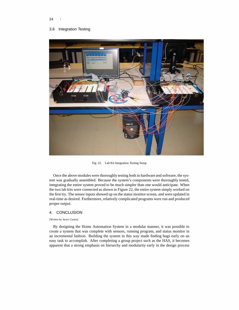
Fig. 22. Lab Kit Integration Testing Setup
Once the above modules were thoroughly testing both in hardware and software, the sys-tem was gradually assembled. Because the system’s components were thoroughly tested,integrating the entire system proved to be much simpler than one would anticipate. Whenthe two lab kits were connected as shown in Figure 22, the entire system simply worked onthe first try. The sensor inputs showed up on the status monitor screen, and were updated inreal-time as desired. Furthermore, relatively complicated programs were run and producedproper output.
4. CONCLUSION
[Written by Javier Castro]
By designing the Home Automation System in a modular manner, it was possible tocreate a system that was complete with sensors, running program, and status monitor inan incremental fashion. Building the system in this way made finding bugs early on aneasy task to accomplish. After completing a group project such as the HAS, it becomesapparent that a strong emphasis on hierarchy and modularity early in the design process

· 25
results in a clear specification. This specification allows the implementers of the systemto keep a clear idea of what tasks need to be accomplished and never get confused bythe complexity of the task at hand. If, while constructing the system, any part failed tobe realized, it was possible to work around the problem and still manage to implement asystem that was working towards the final goal. The lesson learned is that more time spentdesigning results in less time wondering what went wrong with the implementation.
Acknowledgements
The authors would like to sincerely thank the 6.111 course staff for being a tremendouslysupportive resource throughout the course of this project. In particular, many of ChrisTerman’s design suggestions ended up making their way into the final design. Likewise,HyungBin Son’s RS232 interface and guidance throughout the project was invaluable, andColin Weltin-Wu’s support throughout the project was always helpful and is much appre-ciated.