
The need for integrated optical interconnects in electronic
16
Silicon Microphotonics Lionel C. Kimerling MIT Microphotonics Center Massachusetts Institute of Technology Cambridge, MA 02139 ABSTRACT A rebuilding of the world’s information infrastructure is taking place to give instantaneous availability of data, voice and video. This revolution of the Information Age is being gated more by the introduction of new materials and components, than by the design of systems, software and networks. Electrons transmitted through metal wires have an information carrying capacity limited by the resistance and capacitance of the cable and the terminating electronic circuits. Photons transmitted through fiber are capacity limited only by the dispersion of the medium. Each network node that requires transduction from photonics to electronics limits the performance and affordability of the network. The key frontier is the large scale integration and manufacturing of photonic components to enable the distribution of high bit rate optical streams to the individual information appliance. Microphotonics is the platform for large scale, planar integration of optical signal processing capability. INTRODUCTION It is now one-half century since the advent of solid state electronics with the invention of the transistor. Through unparalleled gains in functionality at relatively constant cost, integrated circuits have enabled telecommunications, computation and manufacturing to move to the leading edge of societal change. This revolution has been conducted with “the turn of a single knob”: the shrinking of device dimensions. During the last two decades a new “killer technology” has emerged in the telecommunications field. This photonic technology uses optical fibers for interconnection, and has delivered an exponential increase with time of information carrying capacity to the industry. Photonics has provided unparalleled bandwidth to the backbone of the discrete, point-to-point long distance (Wide Area Network) telephone line technology. However, the circuit architecture (central switching office) that worked so well for voice communications now limits the universal access that is required for Internet and data communications. A single optical fiber, with several hundred gigabits/second of capacity, is limited by electronic processing at each circuit node. To avoid this problem optical signal processors are required: e.g., optical cross-connects and optical add/drop multiplexers. To provide full functionality, these components must be integrated at densities compatible with microelectronic integration. This microphotonics platform represents not only a solution to information access, but it can also solve the problems of bandwidth, pin-out density, reliability and complexity that threaten to end the advance of the silicon integrated circuit technology. A good figure of merit for the performance of microphotonic integrated circuits is (speed)/(power)x(area). The Information Age was ushered into existence by Microelectronics. The future will depend on the networking of databases for universal accessibility. This new Age of Connectivity will require a mating of microelectronic and fiber optic technology through integrated of Microphotonic functionality. 1
Transcript of The need for integrated optical interconnects in electronic
Silicon Microphotonics
Lionel C. Kimerling MIT Microphotonics Center
Massachusetts Institute of Technology Cambridge, MA 02139
ABSTRACT A rebuilding of the world’s information infrastructure is taking place to give instantaneous availability of data, voice and video. This revolution of the Information Age is being gated more by the introduction of new materials and components, than by the design of systems, software and networks. Electrons transmitted through metal wires have an information carrying capacity limited by the resistance and capacitance of the cable and the terminating electronic circuits. Photons transmitted through fiber are capacity limited only by the dispersion of the medium. Each network node that requires transduction from photonics to electronics limits the performance and affordability of the network. The key frontier is the large scale integration and manufacturing of photonic components to enable the distribution of high bit rate optical streams to the individual information appliance. Microphotonics is the platform for large scale, planar integration of optical signal processing capability. INTRODUCTION It is now one-half century since the advent of solid state electronics with the invention of the transistor. Through unparalleled gains in functionality at relatively constant cost, integrated circuits have enabled telecommunications, computation and manufacturing to move to the leading edge of societal change. This revolution has been conducted with “the turn of a single knob”: the shrinking of device dimensions. During the last two decades a new “killer technology” has emerged in the telecommunications field. This photonic technology uses optical fibers for interconnection, and has delivered an exponential increase with time of information carrying capacity to the industry. Photonics has provided unparalleled bandwidth to the backbone of the discrete, point-to-point long distance (Wide Area Network) telephone line technology. However, the circuit architecture (central switching office) that worked so well for voice communications now limits the universal access that is required for Internet and data communications. A single optical fiber, with several hundred gigabits/second of capacity, is limited by electronic processing at each circuit node. To avoid this problem optical signal processors are required: e.g., optical cross-connects and optical add/drop multiplexers. To provide full functionality, these components must be integrated at densities compatible with microelectronic integration. This microphotonics platform represents not only a solution to information access, but it can also solve the problems of bandwidth, pin-out density, reliability and complexity that threaten to end the advance of the silicon integrated circuit technology. A good figure of merit for the performance of microphotonic integrated circuits is (speed)/(power)x(area). The Information Age was ushered into existence by Microelectronics. The future will depend on the networking of databases for universal accessibility. This new Age of Connectivity will require a mating of microelectronic and fiber optic technology through integrated of Microphotonic functionality.
1
The technology pull for integrated optical interconnects in electronic systems is based on cost and performance trends. The cost-per-interconnect increases exponentially with interconnect length: from the shortest interconnects on a chip to the longest interconnects in global telecommunications networks. This economic pressure is a driving force to condense functions locally at the chip, board or system level. Lightwave telecommunications systems utilize silicon transistors to drive gigahertz rate modulation of optical sources. These transistors, together with compound semiconductor lasers and detectors, and silica optical fibers, have increased the system information carrying capacity to the extent that voice and image transmission have enabled the explosive growth of the Internet. This lightwave technology systems driver is potentially the key enabler for extension of chip performance beyond the limits of dimensional scaling. By 2010 microprocessors will have clock frequencies greater than 6 GHz with chip dimensions greater than 3 cm across the diagonal [SIA97]. One key constraint in the conventional scaling of silicon ULSI is the high interconnect-related power dissipation per unit area. Additionally, in future electronic systems, utilization of chip performance will be limited by the crosstalk introduced by high-densities of chip-to-chip electronic interconnects operating at frequencies near 500 MHz. The number of I/O pins per chip, determined by word size and power distribution, will drive cost and will, hence, dictate the future of interconnect architecture. Multiple levels of interconnection are employed at the chip level to minimize area and crosstalk, but long metal interconnects, 1-100 m in width, operating at frequencies of 6 GHz, present process yield, power dissipation and thermal management problems. Universal implementation of copper wiring offers an intermediate solution. Optical interconnects at the board level and for the longest interconnection lines on chip offer a scalable, low cost interconnection architecture with the capability of reducing the number of I/O pins by wavelength division multiplexing. Additionally, these optical links can feature reduced power dissipation and crosstalk at GHz frequencies. OPTICAL INTERCONNECTION Several approaches to optical interconnection have been proposed in the literature. Challenges in materials, optical device design, CMOS receiver circuit design and overall system architecture have been recognized, and some fundamental limits have been presented. Krishnamoorthy et. al., [Krishnamoorthy96] have summarized the limitations of optoelectronic-VLSI (OE-VLSI) using flip-chip bonded MQW modulators coupled with standard Si-CMOS transimpedance-amplifier based receivers. They concluded that the main barriers to continued scaling of OE-VLSI circuits based on modulator technology can be expected to come from the yield of the modulators, the finite laser source power, and the on-chip power dissipation of the I/O circuits. Additionally, they show that the receiver circuits will be a significant source of electrical power dissipation for any OE-VLSI technology that attempts to provide a large number of low-energy, high-speed surface-normal optical links. According to their calculations, an aggregate I/O bandwidth of 0.5 Tb/s with 0.7 m CMOS to 25 Tb/s with future 0.1 m CMOS technologies appears to be possible, despite some relatively conservative assumptions on optoelectronic device performance. Iwata et. al., [Iwata93] compare the signal propagation delay time of optical interconnection to that of electrical interconnection as a function of length and design rule. Their calculations, based on modeling electrical interconnects as a distributed RC line, show that for interconnection lengths greater than 3mm, optical interconnects have much smaller delay times for all of the 0.2 m, 0.5 m or 1 m design rules considered. For example, the delay time of a 20 mm long electrical interconnect with a 0.5 m design rule is over 5 ns, and it exceeds 20 ns with a 0.2 m design rule.
2
Both values are much larger than the 0.1 ns delay of a 20 mm long optical interconnect. They conclude that higher frequency (i.e. higher speed) systems are possible only with optical interconnection, because there is no intrinsic coupling between optical interconnection lines, or between an optical line and an electrical line. In a laboratory report, Miller et. al., [Miller96] convincingly argue that there is a limit on the bit-rate capacity, B, of electrical interconnects. B depends only on the aspect ratio of the interconnect, i.e. the ratio of interconnect length l to the square root of the total cross-sectional area of the interconnect lines, A according to the relation B = 1015 A/l2 bits/s. They arrive at this limit by calculating the bit-rate capacity of electrical lines using the L and C of a coaxial cable as an example to obtain signal propagation velocity. Their conclusions remain unchanged even with the inclusion of skin-effect limited lines with resistive losses. Therefore, miniaturization of electrical interconnects will not help in improving the bit-rate capacity. Optical interconnects have no such aspect ratio limit because loss in optical media is essentially independent of the modulation bit rate, even into the terahertz regime. Long, thin optical interconnects work especially well. For example, a single-mode optical fiber, 125 m in diameter and 15 km long, is able to carry 100Mb/s of data well within expected dispersion limits. However, an equivalent electrical interconnect with similar dimensions can carry less than 0.1b/s of data. This comparison makes a case for using optical signal links for chip packaging operating in the tens of GHz regime. Pin-out density, cost, power dissipation and crosstalk are ultimate limiters to IC chip architectures [Fitzgerald98, Kimerling99]. In current microprocessors, the clock signal is the master controller for all activities and the highest bandwidth interconnect function on the chip. The signal must synchronize every subsystem on the chip, and it determines the number of instructions executed per second. Current electronic designs trade area (capacitance) and power (speed) to provide a clock skew of less than 1% of the clock period. Data input and output to a chip present a slightly different problem. As word sizes increase, 64, then 128, etc. separate inputs and outputs must exist on every chip. This layout problem lies much deeper, though, as the capacitive loads at the end of the pins require larger and larger devices, limiting speed and taking up precious real estate. Additionally, when gate dielectrics reach fundamental scaling limits, electronic circuits will reach a speed plateau determined by transistor gate delay. At that point we envision a paradigm shift to parallelism facilitated by optical interconnection as the favored option for maintaining chip performance roadmap trends. Optical interconnection is a solution to both the clock distribution and data I/O problems. An optical signal can be split without adding delay or skew. Many signals can be multiplexed into one waveguide; even clock and data signals can be combined, reducing the number of required inputs and outputs. Global optical bus networks promise to enable high density interconnection and signal multiplexing while featuring the low crosstalk of photons (as opposed to electrons). MONOLITHIC SILICON MICROPHOTONICS Silicon microphotonics is the optical equivalent of microelectronics for integrated circuits. Photonics enables unlimited interconnection transmission bandwidth. In addition photonic switching promises ultrafast routing and encoding of information for telecommunications and data transmission. The key issue is the integration of photonic components with integrated circuit electronics. Silicon microphotonics utilizes silicon-based materials that are process compatible with standard integrated circuit fabrication methods [Giovane97, Kimerling99].
3
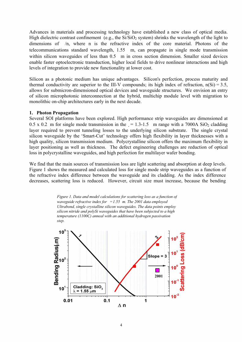
Advances in materials and processing technology have established a new class of optical media. High dielectric contrast confinement (e.g., the Si/SiO2 system) shrinks the wavelength of the light to dimensions of /n, where n is the refractive index of the core material. Photons of the telecommunications standard wavelength, 1.55 m, can propagate in single mode transmission within silicon waveguides of less than 0.5 m in cross section dimension. Smaller sized devices enable faster optoelectronic transduction, higher local fields to drive nonlinear interactions and high levels of integration to provide new functionality at lower cost. Silicon as a photonic medium has unique advantages. Silicon's perfection, process maturity and thermal conductivity are superior to the III-V compounds; its high index of refraction, n(Si) = 3.5, allows for submicron-dimensioned optical devices and waveguide structures. We envision an entry of silicon microphotonic interconnection at the hybrid, multichip module level with migration to monolithic on-chip architectures early in the next decade. 1. Photon Propagation Several SOI platforms have been explored. High performance strip waveguides are dimensioned at 0.5 x 0.2 m for single mode transmission in the = 1.3-1.5 m range with a 7000A SiO2 cladding layer required to prevent tunneling losses to the underlying silicon substrate. The single crystal silicon waveguide by the ‘Smart-Cut’ technology offers high flexibility in layer thicknesses with a high quality, silicon transmission medium. Polycrystalline silicon offers the maximum flexibility in layer positioning as well as thickness. The defect engineering challenges are reduction of optical loss in polycrystalline waveguides, and high perfection for multilayer wafer bonding. We find that the main sources of transmission loss are light scattering and absorption at deep levels. Figure 1 shows the measured and calculated loss for single mode strip waveguides as a function of the refractive index difference between the waveguide and its cladding. As the index difference decreases, scattering loss is reduced. However, circuit size must increase, because the bending
2001
Figure 1. Data and model calculations for scattering loss as a function of waveguide refractive index for =1.55 m. The 2001 data employed Ultrabond, single crystalline silicon waveguides. The data points employ silicon nitride and polySi waveguides that have been subjected to a high temperature (1100C) anneal with an additional hydrogen passivation step.
4
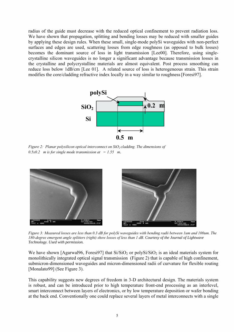
radius of the guide must decrease with the reduced optical confinement to prevent radiation loss. We have shown that propagation, splitting and bending losses may be reduced with smaller guides by applying these design rules. When these small, single-mode polySi waveguides with non-perfect surfaces and edges are used, scattering losses from edge roughness (as opposed to bulk losses) becomes the dominant source of loss in light transmission [Lee00]. Therefore, using single-crystalline silicon waveguides is no longer a significant advantage because transmission losses in the crystalline and polycrystalline materials are almost equivalent. Post process smoothing can reduce loss below 1dB/cm [Lee 01]. A related source of loss is heterogeneous strain. This strain modifies the core/cladding refractive index locally in a way similar to roughness [Foresi97].
0.5 m
0.2 m
polySi
SiO2
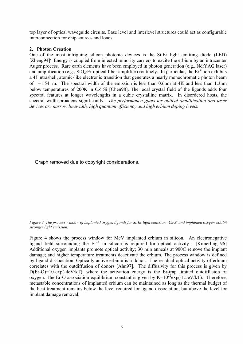
Si
Figure 2: Planar polysilicon optical interconnect on SiO2 cladding. The dimensions of 0.5x0.2 m is for single mode transmission at = 1.55 m. Figure 3: Measured losses are less than 0.3 dB for polySi waveguides with bending radii between 1um and 100um. The 180-degree emergent angle splitters (right) show losses of less than 1 dB. Courtesy of the Journal of LightwaveTechnology. Used with permission. We have shown [Agarwal96, Foresi97] that Si/SiO2 or polySi/SiO2 is an ideal materials system for monolithically integrated optical signal transmission (Figure 2) that is capable of high confinement, submicron-dimensioned waveguides and micron-dimensioned radii of curvature for flexible routing [Monalato99] (See Figure 3). This capability suggests new degrees of freedom in 3-D architectural design. The materials system is robust, and can be introduced prior to high temperature front-end processing as an interlevel, smart interconnect between layers of electronics, or by low temperature deposition or wafer bonding at the back end. Conventionally one could replace several layers of metal interconnects with a single
5
top layer of optical waveguide circuits. Base level and interlevel structures could act as configurable interconnection for chip sources and loads. 2. Photon Creation One of the most intriguing silicon photonic devices is the Si:Er light emitting diode (LED) [Zheng94]. Energy is coupled from injected minority carriers to excite the erbium by an intracenter Auger process. Rare earth elements have been employed in photon generation (e.g., Nd:YAG laser) and amplification (e.g., SiO2:Er optical fiber amplifier) routinely. In particular, the Er3+ ion exhibits a 4f intrashell, atomic-like electronic transition that generates a nearly monochromatic photon beam of =1.54 m. The spectral width of the emission is less than 0.6nm at 4K and less than 1.3nm below temperatures of 200K in CZ Si [Chen98]. The local crystal field of the ligands adds four spectral features at longer wavelengths in a cubic crystalline matrix. In disordered hosts, the spectral width broadens significantly. The performance goals for optical amplification and laser devices are narrow linewidth, high quantum efficiency and high erbium doping levels.
Figure 4. The process window of implanted oxygen ligands for Si:Er light emission. Cz-Si and implanted oxygen exhibit stronger light emission. Figure 4 shows the process window for MeV implanted erbium in silicon. An electronegative ligand field surrounding the Er3+ in silicon is required for optical activity. [Kimerling 96] Additional oxygen implants promote optical activity; 30 min anneals at 900C remove the implant damage; and higher temperature treatments deactivate the erbium. The process window is defined by ligand dissociation. Optically active erbium is a donor. The residual optical activity of erbium correlates with the outdiffusion of donors [Ahn97]. The diffusivity for this process is given by D(Er-O)=103exp(-4eV/kT), where the activation energy is the Er-trap limited outdiffusion of oxygen. The Er-O association equilibrium constant is given by K=1022exp(-1.5eV/kT). Therefore, metastable concentrations of implanted erbium can be maintained as long as the thermal budget of the heat treatment remains below the level required for ligand dissociation, but above the level for implant damage removal.
6
Graph removed due to copyright considerations.
An alternative to implantation is in-situ doping with Er-ligand complexes during silane CVD layer growth. We have explored a variety of metallorganic precursors for this purpose. The main process constraint is the temperature difference between volatilization and transport of the precursor, and the deposition temperature where both the precursor and the silane dissociate. We have used Er(tmhd)3, Er(fod)3 and Er(tmsa)3 as precursors to provide oxygen, fluorine and nitrogen ligands, respectively [Morse96]. All yield strong Er emission lines. Metastable erbium concentrations as high as 2x1021cm-3 have been obtained at deposition temperatures near 600C. The films have a higher quantum efficiency than the best implanted samples. The Er(tmsa)3 has provided the best control of the precursor fragmentation process to give a high yield of Er-ligand complexes in the films. CMOS process integration of Si:Er LEDs has been demonstrated. Er has a low diffusivity in Si, and it is readily oxidized as an external phase. Hence, it does not cross contaminate during processing [Ren93]. Optical waveguides have been integrated with Si:Er LEDs and drive electronics as shown in Figures 5 and 6. Modulation of the MOSFET gate voltage provides direct modulation of the LED light output. The circuit exhibits 20kHz roll-off of the direct modulation frequency due to the long excited state lifetime of Er3+. The mesa design with top contacts allows the Er/O implant and anneal to be independent of the MOSFET thermal budget.
Figure 6: Si:Er LED integration with MOSFET driver.Figure 5: Integration of Si:Er LED and Si waveguide.
A most valuable application of Si:Er devices would be optical amplification. High photon fluxes at local electronic signal distribution nodes reduce the latency associated with amplification and signal conditioning. An Si:Er optical amplifier with direct injection pumping should be a factor of 106 more efficient in excitation than the 980nm optical pump for conventional fiber amplifiers. This property can reduce amplifier size to levels compatible with component integration. Optical amplification is a key function in the optical interconnection paradigm.
7
Image removed due to copyright considerations. Image removed due to copyright considerations.
3. Photon Detection Transduction of photons to electrons is required for the integration of microphotonics with microelectronics. Since photons of energy greater than the silicon band gap can be absorbed
igure 7. Calculated values of absorption coefficient of SiGe alloys
in the 1.1 m < <1.7 m range.
throughout the integrated circuit and inject spurious signals, ‘sub-gap’ energies are preferred.
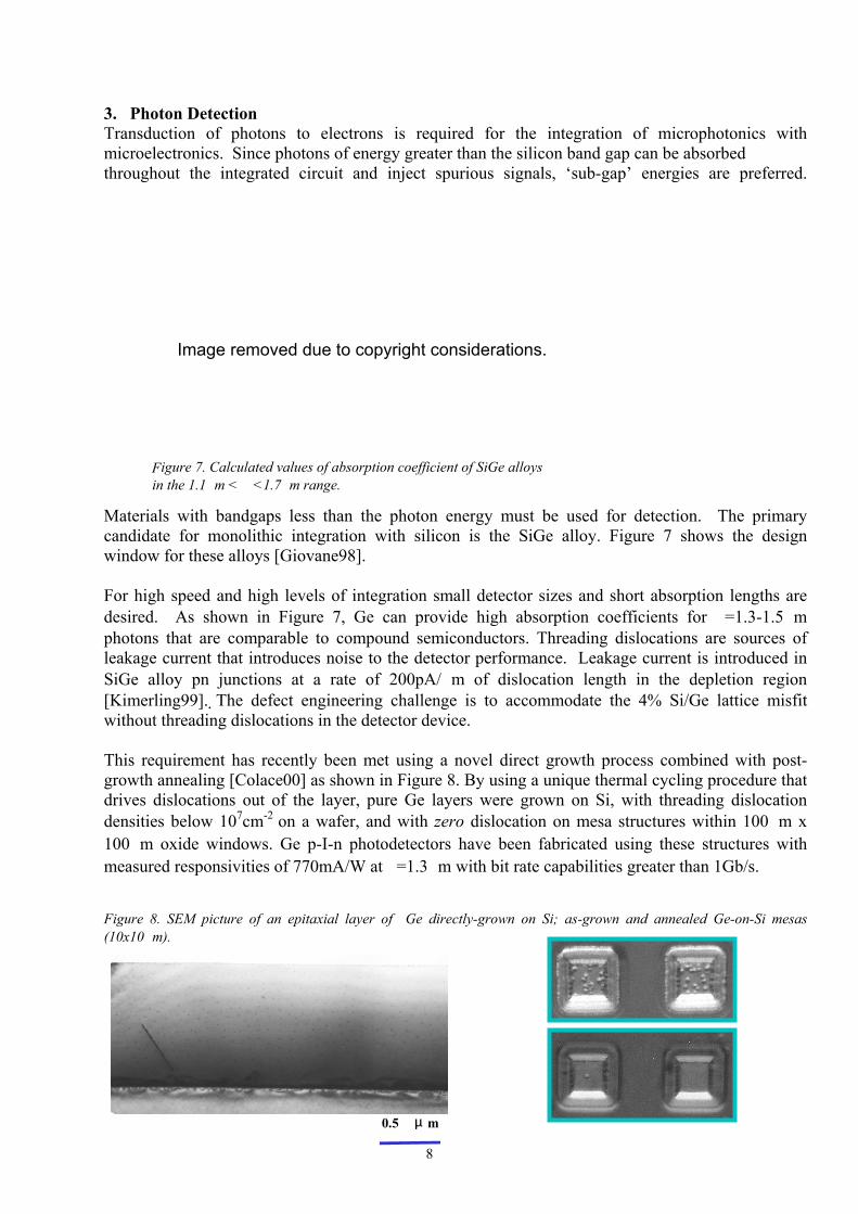
Materials with bandgaps less than the photon energy must be used for detection. The primary candidate for monolithic integration with silicon is the SiGe alloy. Figure 7 shows the design window for these alloys [Giovane98]. For high speed and high levels of integration small detector sizes and short absorption lengths are desired. As shown in Figure 7, Ge can provide high absorption coefficients for =1.3-1.5 m photons that are comparable to compound semiconductors. Threading dislocations are sources of leakage current that introduces noise to the detector performance. Leakage current is introduced in SiGe alloy pn junctions at a rate of 200pA/ m of dislocation length in the depletion region [Kimerling99]. The defect engineering challenge is to accommodate the 4% Si/Ge lattice misfit without threading dislocations in the detector device. This requirement has recently been met using a novel direct growth process combined with post-growth annealing [Colace00] as shown in Figure 8. By using a unique thermal cycling procedure that drives dislocations out of the layer, pure Ge layers were grown on Si, with threading dislocation densities below 107cm-2 on a wafer, and with zero dislocation on mesa structures within 100 m x 100 m oxide windows. Ge p-I-n photodetectors have been fabricated using these structures with measured responsivities of 770mA/W at =1.3 m with bit rate capabilities greater than 1Gb/s. Figure 8. SEM picture of an epitaxial layer of Ge directly-grown on Si; as-grown and annealed Ge-on-Si mesas (10x10 m).
8
0.5 µ m
Image removed due to copyright considerations.
F
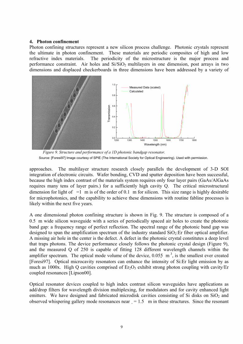
4. Photon confinement Photon confining structures represent a new silicon process challenge. Photonic crystals represent the ultimate in photon confinement. These materials are periodic composites of high and low refractive index materials. The periodicity of the microstructure is the major process and performance constraint. Air holes and Si/SiO2 multilayers in one dimension, post arrays in two dimensions and displaced checkerboards in three dimensions have been addressed by a variety of
approaches. The multilayer structure research closely parallels the development of 3-D SOI integration of electronic circuits. Wafer bonding, CVD and sputter deposition have been successful, because the high index contrast of the materials system requires only four layer pairs (GaAs/AlGaAs requires many tens of layer pairs.) for a sufficiently high cavity Q. The critical microstructural dimension for light of =1 m is of the order of 0.1 m for silicon. This size range is highly desirable for microphotonics, and the capability to achieve these dimensions with routine fabline processes is likely within the next five years.
1200 1300 1400 1500 1600 1700 18000.0
0.2
0.4
0.6
0.8
1.0 Measured Data (scaled) Calculated
Tran
smis
sion
Wavelength (nm)
Figure 9. Structure and performance of a 1D photonic bandgap resonator.
A one dimensional photon confining structure is shown in Fig. 9. The structure is composed of a 0.5 m wide silicon waveguide with a series of periodically spaced air holes to create the photonic band gap: a frequency range of perfect reflection. The spectral range of the photonic band gap was designed to span the amplification spectrum of the industry standard SiO2:Er fiber optical amplifier. A missing air hole in the center is the defect. A defect in the photonic crystal constitutes a deep level that traps photons. The device performance closely follows the photonic crystal design (Figure 9), and the measured Q of 250 is capable of fitting 128 different wavelength channels within the amplifier spectrum. The optical mode volume of the device, 0.055 m 3, is the smallest ever created [Foresi97]. Optical microcavity resonators can enhance the intensity of Si:Er light emission by as much as 1000x. High Q cavities comprised of Er2O3 exhibit strong photon coupling with cavity/Er coupled resonances [Lipson00]. Optical resonator devices coupled to high index contrast silicon waveguides have applications as add/drop filters for wavelength division multiplexing, for modulators and for cavity enhanced light emitters. We have designed and fabricated microdisk cavities consisting of Si disks on SiO2 and observed whispering gallery mode resonances near = 1.5 m in these structures. Since the resonant
9
Source: [Foresi97] Image courtesy of SPIE (The International Society for Optical Engineering). Used with permission.
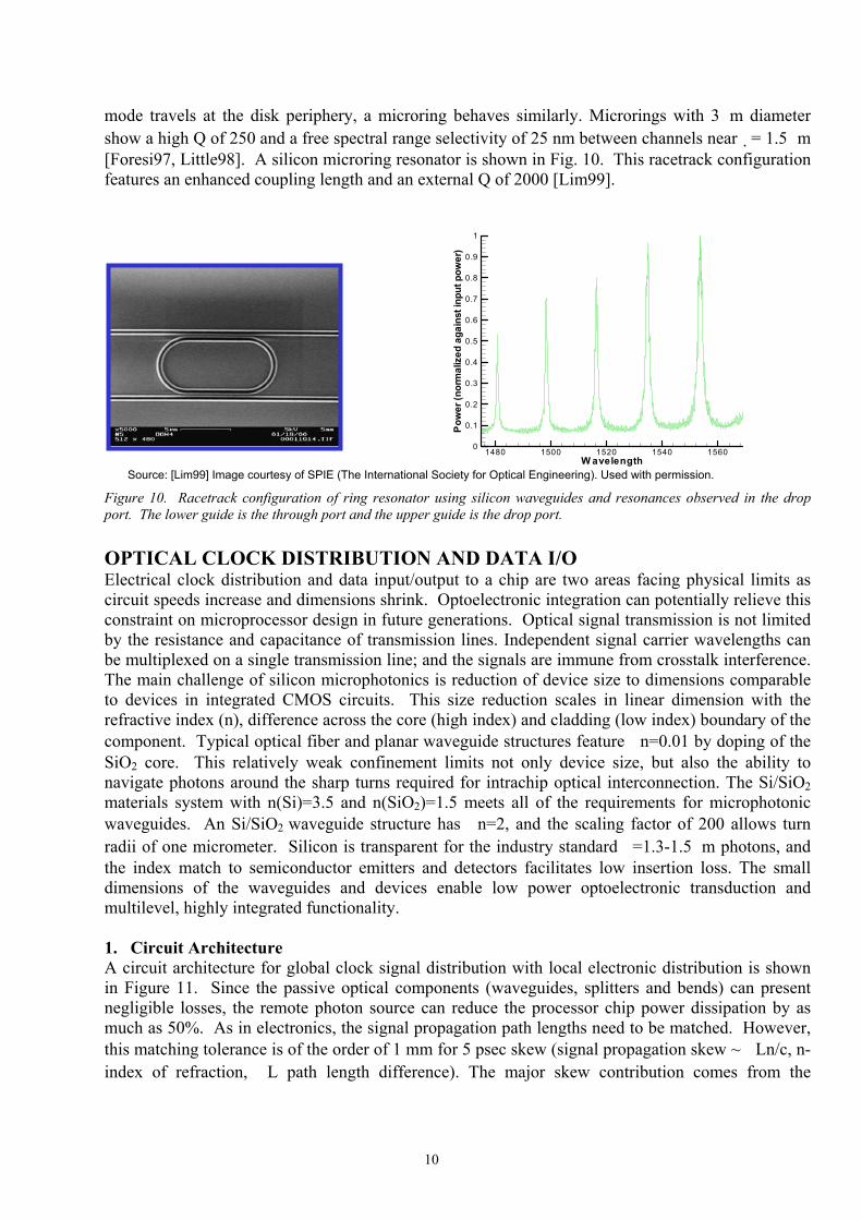
mode travels at the disk periphery, a microring behaves similarly. Microrings with 3 m diameter show a high Q of 250 and a free spectral range selectivity of 25 nm between channels near = 1.5 m [Foresi97, Little98]. A silicon microring resonator is shown in Fig. 10. This racetrack configuration features an enhanced coupling length and an external Q of 2000 [Lim99].
WavelengthPower(normalizedagainstinputpower)
1480 1500 1520 1540 15600
0.1
0.2
0.3
0.4
0.5
0.6
0.7
0.8
0.9
1
3x6um racetrack (.2 um gap) Q~800 Figure 10. Racetrack configuration of ring resonator using silicon waveguides and resonances observed in the drop port. The lower guide is the through port and the upper guide is the drop port. OPTICAL CLOCK DISTRIBUTION AND DATA I/O Electrical clock distribution and data input/output to a chip are two areas facing physical limits as circuit speeds increase and dimensions shrink. Optoelectronic integration can potentially relieve this constraint on microprocessor design in future generations. Optical signal transmission is not limited by the resistance and capacitance of transmission lines. Independent signal carrier wavelengths can be multiplexed on a single transmission line; and the signals are immune from crosstalk interference. The main challenge of silicon microphotonics is reduction of device size to dimensions comparable to devices in integrated CMOS circuits. This size reduction scales in linear dimension with the refractive index (n), difference across the core (high index) and cladding (low index) boundary of the component. Typical optical fiber and planar waveguide structures feature n=0.01 by doping of the SiO2 core. This relatively weak confinement limits not only device size, but also the ability to navigate photons around the sharp turns required for intrachip optical interconnection. The Si/SiO2 materials system with n(Si)=3.5 and n(SiO2)=1.5 meets all of the requirements for microphotonic waveguides. An Si/SiO2 waveguide structure has n=2, and the scaling factor of 200 allows turn radii of one micrometer. Silicon is transparent for the industry standard =1.3-1.5 m photons, and the index match to semiconductor emitters and detectors facilitates low insertion loss. The small dimensions of the waveguides and devices enable low power optoelectronic transduction and multilevel, highly integrated functionality.
1. Circuit Architecture A circuit architecture for global clock signal distribution with local electronic distribution is shown in Figure 11. Since the passive optical components (waveguides, splitters and bends) can present negligible losses, the remote photon source can reduce the processor chip power dissipation by as much as 50%. As in electronics, the signal propagation path lengths need to be matched. However, this matching tolerance is of the order of 1 mm for 5 psec skew (signal propagation skew ~ Ln/c, n-index of refraction, L path length difference). The major skew contribution comes from the
10
Source: [Lim99] Image courtesy of SPIE (The International Society for Optical Engineering). Used with permission.
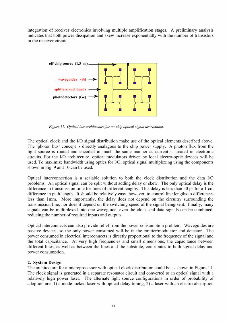
integration of receiver electronics involving multiple amplification stages. A preliminary analysis indicates that both power dissipation and skew increase exponentially with the number of transistors in the receiver circuit.
off-chip source (1.3 m)
photodetectors (Ge)
splitters and bends
waveguides (Si)
Figure 11. Optical bus architecture for on-chip optical signal distribution.
The optical clock and the I/O signal distribution make use of the optical elements described above. The ‘photon bus’ concept is directly analagous to the chip power supply. A photon flux from the light source is routed and encoded in much the same manner as current is treated in electronic circuits. For the I/O architecture, optical modulators driven by local electro-optic devices will be used. To maximize bandwidth using optics for I/O, optical signal multiplexing using the components shown in Fig. 9 and 10 can be used. Optical interconnection is a scalable solution to both the clock distribution and the data I/O problems. An optical signal can be split without adding delay or skew. The only optical delay is the difference in transmission time for lines of different lengths. This delay is less than 50 ps for a 1 cm difference in path length. It should be relatively easy, however, to control line lengths to differences less than 1mm. More importantly, the delay does not depend on the circuitry surrounding the transmission line, nor does it depend on the switching speed of the signal being sent. Finally, many signals can be multiplexed into one waveguide; even the clock and data signals can be combined, reducing the number of required inputs and outputs. Optical interconnects can also provide relief from the power consumption problem. Waveguides are passive devices, so the only power consumed will be in the emitter/modulator and detector. The power consumed in electrical interconnects is directly proportional to the frequency of the signal and the total capacitance. At very high frequencies and small dimensions, the capacitance between different lines, as well as between the lines and the substrate, contributes to both signal delay and power consumption. 2. System Design The architecture for a microprocessor with optical clock distribution could be as shown in Figure 11. The clock signal is generated in a separate resonator circuit and converted to an optical signal with a relatively high power laser. The alternate light source configurations in order of probability of adoption are: 1) a mode locked laser with optical delay timing, 2) a laser with an electro-absorption
11
modulator, 3) a laser directly pumped by oscillator/power supply. This signal can originate on a dedicated source chip, or die in an MCM configuration, and the clock signal can be distributed to all synchronized chips in the system. The clock signal is received on-chip optically and split optically (10-100 times) in distribution to the major sections of the chip. At each major section the signal is converted to an electrical signal through a detector and receiver circuitry to yield the appropriate voltage level, and it is distributed electrically to subsections. Measured data on existing silicon avalanche photo detectors (APD) show that a total skew of 100ps can be achieved with a silicon APD and one stage of amplification with an incident optical power of 1 W [Khalil 89]. Since APD detectors require high voltages to operate, which may be incompatible with high levels of integration, PIN detectors with a higher optical power requirement may be preferred. Starting with the 1 W required power at each detector, the specifications for the emitter and waveguide depend on the total fanout level and the coupling and distribution losses. For 16 levels of fanout with a 10dB loss budget, the coupled emitter power must be 160 W. For a p-i-n detector a factor of 10 more power, 1.6mW, is required. The requirements for data transmission are somewhat less stringent. In order to achieve a bit error rate of 10-9 from a silicon APD detector, an incident photon flux of 125 photons/bit, or 1.65x10⁻⁸W is required [Saleh and Teich 91]. Thus, for data transmission, two orders of magnitude less optical power is required than for clock distribution. For the clock application with current architectures, the switching of individual latches dominates the current requirements. More than 100 A can be required to switch one transistor latch at a 1nS clock cycle time, a 100pS skew limit and a 1V power supply level. Electronic amplification after the photodetector can only add to skew. Therefore, a major design consideration for optical clock is the depth of optical distribution. “A million points of light” represents the lowest skew configuration, but a shallower fanout with local electronic distribution could demand less total power. Optical data transmission between chips illustrates an opportunity to take advantage of the high optical bandwidth. By using a large array of emitters and detectors operating at high modulation frequencies, data transmission in the terabaud region could be realized. Rather than requiring hundreds of fibers running between the chips, which would be difficult and expensive, free space connections with mirrors and lenses are likely to be preferable. The remaining issues are the operating wavelength and the waveguide materials. A photon wavelength of 1.5 micron is compatible with telecommunications standard, and since its energy is below the bandgap of silicon, there is no effect of stray light on device performance. One problem this wavelength creates is detector materials. Silicon is an excellent material for APDs operating at 0.88 m), but it cannot be used at 1.5 m. Germanium possesses the appropriate bandgap, but its devices will have a higher dark current, raising the power required at the detector to maintain a bit error rate of 10-9. Doped silicon dioxide waveguides are compatible with optical fiber interconnection between chips. However, the low refractive index difference between the core and the cladding of these structures can lead to very high bending losses. As a result, turning mirrors must be incorporated to route the signal around sharp bends. At the 1.5 m wavelength, silicon waveguides clad with silicon dioxide can be used. These waveguides can accommodate very small radii of curvature turns, r<10 m with low loss, due to the large index difference between the waveguide and the cladding. An important, but often neglected, part of the silicon optoelectronic circuit is the packaging. This packaging issue involves the integration of all on-chip optical components as well as the coupling to
12
off-chip sources. Critical tapering of waveguides is required for the coupling of optical fiber to on-chip nano-waveguides. Every internal coupling must be optimized to reduce insertion loss of the components. Options for packaging and integration need careful evaluation. SUMMARY Component and circuit engineering for microelectronics is structured to meet the constraints posed by carrier transport and lifetime, and electric field design criteria. One is concerned with the control of scattering sites, recombination centers and localized sources of dielectric breakdown and leakage current. Microphotonics focuses concern on photon creation, propagation and optoelectronic detection. The figures of merit for photonics are optical power transmission loss, quantum efficiency of photonic/electronic transduction and optical microcavity Q (photon lifetime). Photon absorption and scattering are sources of loss. Localized dipole coupling determines the efficiency of photon generation and detection. Precise dimensional control at length scales of the photon wavelength in the material (wavelength divided by the refractive index) is necessary. These metrics provide the engineering design constraints. This paper has reviewed the principles and progress in component and circuit engineering for silicon microphotonic emitters, waveguides, detectors and optical resonators. We envision an architecture for the future where global clock distribution will enable parallelism among chips and across the entire chip. The ultimate limiter to such an architecture has been the skew-compensating electronic circuitry needed to achieve uniform signal delay. To circumvent this “electronic” limitation, we need to have several minichips within the chips. Each minichip locally performs the electronic logic functions required by the device. For this vision to become a reality in the future, signals have to be communicated between minichips over long distances (>10 mm) without skew. Optical interconnects provide an optimal solution to this “electronic” limitation. The fundamental limit of the speed of =1.5 m light in silicon waveguides is a signal propagation delay at about 100 ps/cm. By designing clock distribution interconnects to be the same length, high frequency clock distribution over long distances (>10 mm) as well as over shorter on-chip distances, can be achieved. The fundamental quantum limit of an ideal photodetector with unity quantum efficiency and no dark current is 20 photons/bit for a bit-error-rate (BER) of 10-9. The envisioned entry technology architecture, Figure 11, consists of off-chip light sources, on-chip optical buss signals for clock and data; on-chip modulators to encode data; on-chip detectors to transduce optical clock signals for local electronic distribution; and optical add/drop filters for MUX/DEMUX. A complete appraisal of silicon microphotonic interconnection, requires detailed analysis of the issues of speed, area and power. Evaluation of an electrical interconnect approach involves optimization of materials, wiring designs, and systems architecture. For the evaluation of optical interconnects, one must to optimize each optical component and the integration of the components to retain the benefit of high bandwidth, minimal crosstalk and low power consumption. Optical impedance matching is critical to minimization of insertion loss and standing wave reflections. Large scale monolithic integration has the potential of solving an untenable insertion loss issue that is orders of magnitude greater than exists in current point-to-point communications. The principles for integration must be established early in the technology with simple circuit layouts. Together, this new class of devices constitutes a gateway to on-chip and interchip optical interconnection, and a potential solution to the integrated circuit, interconnection bottleneck. It is interesting then to think of the optoelectronic system design as the driving technology of the future with current chip-size Si CMOS as the basic units of tomorrow. The optoelectronic
13
interconnection and hybrid chip integration will be the back end of tomorrow. In other words, the interconnection hierarchy above the current chip-level (“the board”) becomes the new “chip” of tomorrow. Additionally, SOI wafer bonding and solder bump die attach can be major enablers of hybrid optoelectronic to electronic integration. The industries that possess this design and manufacturing capability for integrated optical interconnects will be the leaders of semiconductor electronics of tomorrow. Acknowledgements I am indebted to the students and colleagues listed in the references who inspired and implemented this work. Professor Hermann Haus and Dr. Anu Agarwal, in particular, were instrumental in developing concepts for integration and in writing. This research was supported by the NSF-MRSEC under contract DMR9808941, AFOSR under contract F49620-95-1-0312, the Semiconductor Research Corporation, and the MARCO Interconnect Focus Center. References [Agarwal96] “Low-loss polycrystalline silicon waveguides for silicon photonics”, Anuradha M. Agarwal, Ling Liao, James S. Foresi, Marcie R. Black, Xiaoman Duan and L. C. Kimerling, J. Appl. Phys. 80 (11), 1 December 1996. [Ahn97] “Electrical Study of Crystalline Silicon Coimplanted with Erbium and Oxygen,” S. Ahn, J. Palm, B. Zheng, X. Duan, A. Agarwal, S. Nelson, J. Michel, L.C. Kimerling, Proceedings of the SPIE “Photonics West” Symposium, Vol.3007, San Jose, CA (February 1997) pp 144-151. [Chen98] “ Erbium-doped polycrystalline silicon light emitters for resonant microcavity devices,” T. Chen, A.M. Agarwal, L.M. Giovane, J.S. Foresi, L. Liao, D.R. Lim, M.T. Morse, E.J. Ouellette, S.H. Ahn, X. Duan, J. Michel, L.C. Kimerling, in “Light-Emitting Diodes: Research, Manufacturing, and Applications II,” Proceedings of the SPIE “Photonics West” Symposium, San Jose, CA January 1998 (Ed) Fred Schubert, Vol. 3279, (1998) pp. 136-145. [Colace00] “Efficient, High Speed Near Infrared Ge Photodetectors Integrated on a Si substrate,” L. Colace, G. Masini, G. Assanto, H.C. Luan, K. Wada and L.C. Kimerling, Applied Phys. Letters, Vol 76 1231 (2000). [Fitzgerald98] “Silicon-based microphotonics and integrated optoelectronics”, E. A. Fitzgerald and L. C. Kimerling, MRS Bulletin, Volume 23, Number 4, Page 39, April 1998. [Foresi97] “Small radius bends and large angle splitters in SOI waveguides”, J. S. Foresi, D. R. Lim, A. M. Agarwal, L. C. Kimerling, M. Tavassoli, M. Cox, M. Cao and W. Greene, Proceedings of the SPIE “Photonics West” Symposium, San Jose, Vol. 3007, pp 112-118, February 1997. [Giovane97] “Materials For Monolithic Silicon Microphotonics,” L.M. Giovane, D.R. Lim, S.H. Ahn, T.D. Chen, J.S. Foresi, L. Liao, E.J.Oulette, A.M. Agarwal, X. Duan, J. Michel, A. Thilderkvist, L.C. Kimerling, Proceedings of the MRS 1997 Fall Meeting, Boston, MA, December 1997 Vol.486(1998) pp 45-56. [Iwata93] “Optical Interconnections as a New LSI Technology”, Atsushi Iwata and Izuo Hayashi, IEICE Trans. Electron., Vol E76-C, No. 1, January 1993.
14
[Kerns98] “The Silicon Diode Under Avalanche Breakdown as a Light Emitting Source for VLSI Optical Interconnect”, D. V. Kerns, K. Arora, S. Kurinec, and W. Power, Proceedings of 21st Southeastern Symposium on System Theory (SSST-89), March 1989, Tallahassee, FL. [Khalil89] SPIE Vol. 1178 (1989), pp 171-176. [Kimerling94] “Erbium-doped silicon for integrated optical interconnects,” L. C. Kimerling, D. M. Koker, B. Zheng, F. Y. G. Ren, J. Michel, Semiconductor Silicon 1994, H. R. Huff, W. Bergholz and K. Sumino, Eds. (The Electrochemical Society, Pennington, N. J.,1994) p. 486. [Kimerling 96] “Light Emission from Silicon”, Lionel C. Kimerling, K. D. Kolenbrander, J. Michel, J. Palm and L. M. Giovane, Solid State Physics 50, 333 (1996). [Kimerling99] “Defect Engineering for Silicon Microphotonics”, A. Agarwal, J.S. Foresi, L.M. Giovane, L. Liao, J. Michel, K. Wada, and L. C. Kimerling, Defects in Silicon III, T. Abe, W. M. Bullis, S. Kobayashi, W. Lin and P. Wagner, Eds. (The Electrochemical Society, Pennington, NJ, 1999) p. 215. [Krishnamoorthy96] “Scaling Optoelectronic-VLSI Circuits into the 21st Century: A Technology Roadmap”, Ashok V. Krishnamoorthy and David A. B. Miller, IEEE Journal of Selected Topics in Quantum Electronics, Vol. 2, No. 1, April 1996. [Krishnamoorthy96-2] “Firehose architectures for free-space optically-interconnected VLSI circuits”, Ashok V. Krishnammorthy and D. A. B. Miller, Ginzton Laboratory Report No. 5474, Stanford University, Stanford, CA, November 1996. [Monalato99] “High-Density Integrated Optics", C. Manolatou, Steven G. Johnson, Shanhui Fan, Pierre Villeneuve,H.A. Haus and J.D. Joannopoulos, Journal of Lightwave Technology, 17, 1682 (1999). [Lee00] “Effects of Size and Roughness on Light Transmission in Si/SiO2 Waveguides: experiments and models”, K.K. Lee, D.R. Lim, H-C Luan, A. Agarwal, J. Foresi and L.C. Kimerling, Applied Phys. Lett. 77, 1617 (2000). [Lee01] “Fabrication of Ultra-low Loss Si/SiO2 Waveguides by Roughness Reduction”, K. K. Lee, D. R. Lim, and L. C. Kimerling; J. Shin, F. Cerrina, Optics Letters 26, 1888 (2001). [Lim99] “Micron-sized channel dropping filters using Si waveguide devices”, D. Lim, B.E. Little, K. Lee, M. Morse, H. Fujimoto, H.A. Haus and L.C. Kimerling, Proc. SPIE 3847, 65 (1999). [Lipson00] “Er3+ in strong light confining microcavity,” M. Lipson and L. C. Kimerling, Applied Phys. Lett. 77, 1150 (2000). [Little98] “Ultra-Compact Si-SiO2 microring Resonator Optical Channel Dropping Filters,” IEEE Photonics Technology Letters, Vol. 10 (4), pp. 549-551, April 1998.
15
16
[Miller96] “Limit to the Bit-Rate Capacity of Electrical Interconnects from the Aspect Ratio of the System Architecture”, D.A.B. Miller and H. M. Ozaktas, Ginzton Laboratory Report No. 5458, Stanford University, Stanford, CA, October 1996. [Morse96] “Properties of Ion-Implanted and UHV-CVD Grown Si:Er,” M. Morse, B. Zheng, J. Palm, X. Duan, L.C. Kimerling, Proceedings of the MRS Spring Meeting, Vol. 422 (1996) pp 41-46. [Ren93] “IC Compatible Processing of Si:Er for Optoelectronics”, F. Y. G. Ren, J. Michel, Q. Sun-Paduano, B. Zheng, H. Kitagawa, D. C. Jacobson, J. M. Poate and L. C. Kimerling, Proceedings of the MRS Spring Meeting, Vol. 298 (1993) pp 415-423. [SIA97] The National Technology Roadmap For Semiconductors 1997 Edition, SIA Semiconductor Industry Association (San Jose, CA 1997) pp 1-196. [Zheng94] “Room Temperature Sharp Line Electroluminescence at = 1.54 µm from an Erbium doped, Silicon Light-emitting Diode,” B. Zheng, J. Michel, F. Y. G. Ren, D. C. Jacobson, J. M. Poate, and L. C. Kimerling, Applied Physics Letters, 64 2842 (1994).