System simulation methodology of optical interconnects for high
19
System simulation methodology of optical interconnects for high- performance computing systems Avinash Karanth Kodi 1, * and Ahmed Louri 2,3 1 Department of Electrical Engineering and Computer Science, Ohio University, Athens, Ohio 45701, USA 2 Department of Electrical and Computer Engineering, University of Arizona, Tucson, Arizona 85721, USA 3 E-mail: [email protected] * Corresponding author: [email protected] Received September 29, 2007; accepted October 5, 2007; published November 6, 2007 Doc. ID 83117 The relentless quest for processing speed in the range of teraflops and beyond has accelerated the need for scalable, parallel, high-performance computing (HPC) systems. To meet this high bandwidth and low power requirements, op- tical interconnect-based system architectures are being implemented by the HPC industry. While computer-aided design tools have significantly assisted electronic system simulation, the field of system level optoelectronics model- ing has lagged behind owing to lack of simulation methodologies and tools. This paper explores the design space of developing OPTISIM, a system level modeling and simulation methodology of optical interconnects for HPC sys- tems. OPTISIM can provide computer architects, designers, and researchers a highly optimized, efficient, and accurate discrete-event environment to test various research hypotheses on HPC systems with power-performance impli- cations. For any given optical interconnect architecture with optical transceiv- ers, wavelength assignment, and traffic patterns, OPTISIM provides end us- ers with network throughput, average latency, power loss, power consumption, and signal strength at the output. The proposed OPTISIM simu- lation methodology is explained with a case study on the performance of an optical HPC architecture called RAPID. © 2007 Optical Society of America OCIS codes: 200.0200, 200.4650. 1. Introduction During the past few years, the computer and communication industries have recog- nized that short-range optical interconnects could potentially provide a cost-effective solution to the increasing bandwidth demands of high-performance computing (HPC) systems [1,2]. Optical interconnects offer several well-known advantages such as higher spatial and temporal bandwidths, lower cross talk independent of data rates, higher interconnect densities, better signal integrity at high frequencies, lower signal attenuation, and lower power requirements at higher bit rates [3,4]; all of which could potentially enhance the scalability and performance of HPC systems. Modeling and simulation play a very pivotal role in the design of any HPC system [5]. Computer-aided design (CAD) tools are essential to optimize design and system parameters to reduce the fabrication cycle time and end-product cost. While electronic system simulation has made significant progress, the field of optoelectronics modeling has lagged behind due to lack of simulation methodology and tools. Although optoelec- tronic tools exist that can be used for simulating and designing optical interconnects, they are either suitable for optical link level and not for system level simulation, or they are intended for electrical interconnects and are used for the lack of tools more suitable for optical interconnects’ unique needs. The end-to-end system design and simulation of optical interconnects for HPC sys- tems for intraboard, board-to-board, and backplane applications can be addressed at different levels of abstraction, namely the functional–link level and the system level as shown in Fig. 1. Prior research work in the field of optoelectronics simulation has focused primarily at the link or at the functional level. The results [or outputs as shown in Fig. 1(a)] that are desirable from the simulation of an optical link include signal waveforms, eye diagrams, deterministic and random jitter, signal-to-noise Vol. 6, No. 12 / December 2007 / JOURNAL OF OPTICAL NETWORKING 1282 1536-5379/07/121282-19/$15.00 © 2007 Optical Society of America
Transcript of System simulation methodology of optical interconnects for high

Vol. 6, No. 12 / December 2007 / JOURNAL OF OPTICAL NETWORKING 1282
System simulation methodology ofoptical interconnects for high-
performance computing systems
Avinash Karanth Kodi1,* and Ahmed Louri2,3
1Department of Electrical Engineering and Computer Science, Ohio University, Athens,Ohio 45701, USA
2Department of Electrical and Computer Engineering, University of Arizona, Tucson,Arizona 85721, USA
3E-mail: [email protected]*Corresponding author: [email protected]
Received September 29, 2007; accepted October 5, 2007;published November 6, 2007 �Doc. ID 83117�
The relentless quest for processing speed in the range of teraflops and beyondhas accelerated the need for scalable, parallel, high-performance computing(HPC) systems. To meet this high bandwidth and low power requirements, op-tical interconnect-based system architectures are being implemented by theHPC industry. While computer-aided design tools have significantly assistedelectronic system simulation, the field of system level optoelectronics model-ing has lagged behind owing to lack of simulation methodologies and tools.This paper explores the design space of developing OPTISIM, a system levelmodeling and simulation methodology of optical interconnects for HPC sys-tems. OPTISIM can provide computer architects, designers, and researchers ahighly optimized, efficient, and accurate discrete-event environment to testvarious research hypotheses on HPC systems with power-performance impli-cations. For any given optical interconnect architecture with optical transceiv-ers, wavelength assignment, and traffic patterns, OPTISIM provides end us-ers with network throughput, average latency, power loss, powerconsumption, and signal strength at the output. The proposed OPTISIM simu-lation methodology is explained with a case study on the performance of anoptical HPC architecture called RAPID. © 2007 Optical Society of America
OCIS codes: 200.0200, 200.4650.
1. IntroductionDuring the past few years, the computer and communication industries have recog-nized that short-range optical interconnects could potentially provide a cost-effectivesolution to the increasing bandwidth demands of high-performance computing (HPC)systems [1,2]. Optical interconnects offer several well-known advantages such ashigher spatial and temporal bandwidths, lower cross talk independent of data rates,higher interconnect densities, better signal integrity at high frequencies, lower signalattenuation, and lower power requirements at higher bit rates [3,4]; all of which couldpotentially enhance the scalability and performance of HPC systems.
Modeling and simulation play a very pivotal role in the design of any HPC system[5]. Computer-aided design (CAD) tools are essential to optimize design and systemparameters to reduce the fabrication cycle time and end-product cost. While electronicsystem simulation has made significant progress, the field of optoelectronics modelinghas lagged behind due to lack of simulation methodology and tools. Although optoelec-tronic tools exist that can be used for simulating and designing optical interconnects,they are either suitable for optical link level and not for system level simulation, orthey are intended for electrical interconnects and are used for the lack of tools moresuitable for optical interconnects’ unique needs.
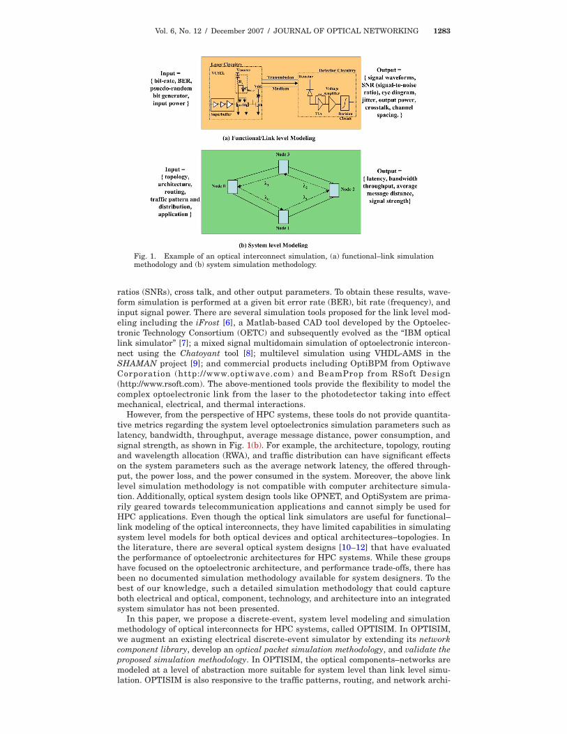
The end-to-end system design and simulation of optical interconnects for HPC sys-tems for intraboard, board-to-board, and backplane applications can be addressed atdifferent levels of abstraction, namely the functional–link level and the system level asshown in Fig. 1. Prior research work in the field of optoelectronics simulation hasfocused primarily at the link or at the functional level. The results [or outputs asshown in Fig. 1(a)] that are desirable from the simulation of an optical link includesignal waveforms, eye diagrams, deterministic and random jitter, signal-to-noise
1536-5379/07/121282-19/$15.00 © 2007 Optical Society of America
Vol. 6, No. 12 / December 2007 / JOURNAL OF OPTICAL NETWORKING 1283
ratios (SNRs), cross talk, and other output parameters. To obtain these results, wave-form simulation is performed at a given bit error rate (BER), bit rate (frequency), andinput signal power. There are several simulation tools proposed for the link level mod-eling including the iFrost [6], a Matlab-based CAD tool developed by the Optoelec-tronic Technology Consortium (OETC) and subsequently evolved as the “IBM opticallink simulator” [7]; a mixed signal multidomain simulation of optoelectronic intercon-nect using the Chatoyant tool [8]; multilevel simulation using VHDL-AMS in theSHAMAN project [9]; and commercial products including OptiBPM from OptiwaveCorporation (http://www.optiwave.com) and BeamProp from RSoft Design(http://www.rsoft.com). The above-mentioned tools provide the flexibility to model thecomplex optoelectronic link from the laser to the photodetector taking into effectmechanical, electrical, and thermal interactions.
However, from the perspective of HPC systems, these tools do not provide quantita-tive metrics regarding the system level optoelectronics simulation parameters such aslatency, bandwidth, throughput, average message distance, power consumption, andsignal strength, as shown in Fig. 1(b). For example, the architecture, topology, routingand wavelength allocation (RWA), and traffic distribution can have significant effectson the system parameters such as the average network latency, the offered through-put, the power loss, and the power consumed in the system. Moreover, the above linklevel simulation methodology is not compatible with computer architecture simula-tion. Additionally, optical system design tools like OPNET, and OptiSystem are prima-rily geared towards telecommunication applications and cannot simply be used forHPC applications. Even though the optical link simulators are useful for functional–link modeling of the optical interconnects, they have limited capabilities in simulatingsystem level models for both optical devices and optical architectures–topologies. Inthe literature, there are several optical system designs [10–12] that have evaluatedthe performance of optoelectronic architectures for HPC systems. While these groupshave focused on the optoelectronic architecture, and performance trade-offs, there hasbeen no documented simulation methodology available for system designers. To thebest of our knowledge, such a detailed simulation methodology that could captureboth electrical and optical, component, technology, and architecture into an integratedsystem simulator has not been presented.
In this paper, we propose a discrete-event, system level modeling and simulationmethodology of optical interconnects for HPC systems, called OPTISIM. In OPTISIM,we augment an existing electrical discrete-event simulator by extending its networkcomponent library, develop an optical packet simulation methodology, and validate theproposed simulation methodology. In OPTISIM, the optical components–networks aremodeled at a level of abstraction more suitable for system level than link level simu-lation. OPTISIM is also responsive to the traffic patterns, routing, and network archi-
Fig. 1. Example of an optical interconnect simulation, (a) functional–link simulationmethodology and (b) system simulation methodology.
Vol. 6, No. 12 / December 2007 / JOURNAL OF OPTICAL NETWORKING 1284
tecture. Given that power consumption in interconnection networks is increasing,OPTISIM models different transmitter and receiver designs, thereby providing powermodels that can be incorporated at the system level. The significant advantages ofOPTISIM include (1) efficient component modeling: each optical component or deviceis modeled independently at a level of abstraction that minimizes the computationalrequirements, while attaining the required system level simulation accuracy and pre-cision; (2) accurate latency modeling: transmission, propagation, and receiver delaysare accumulated to provide accurate optical packet latency; (3) optoelectronic model-ing: as future HPC systems will consist of optical components (transmitter, receiver,medium) and electronic components (buffers, switches, queues), our proposed method-ology incorporates both technologies in the network design to understand cost-performance trade-offs; (4) optoelectronic power modeling: power modeling of opticalinterconnects evaluates the power consumed in the links the different transmittersand receiver designs and at varying bit rates; (5) expandability: active–passive opticalcomponents can be easily added to the simulator based on number of inputs, outputs,and expected functionality; and (6) Extensibility: the designed optical interconnectsimulation framework can be easily integrated with other complex computer architec-ture system simulators for distributed and parallel computers.
For any given optical interconnect architecture with optical transceivers, wave-length assignment, and traffic patterns, OPTISIM provides end users with networkthroughput, average latency, power loss, power consumption, and signal strength asthe output. In what follows, the system simulation methodology of optical intercon-nects is explained in detail with a case study.
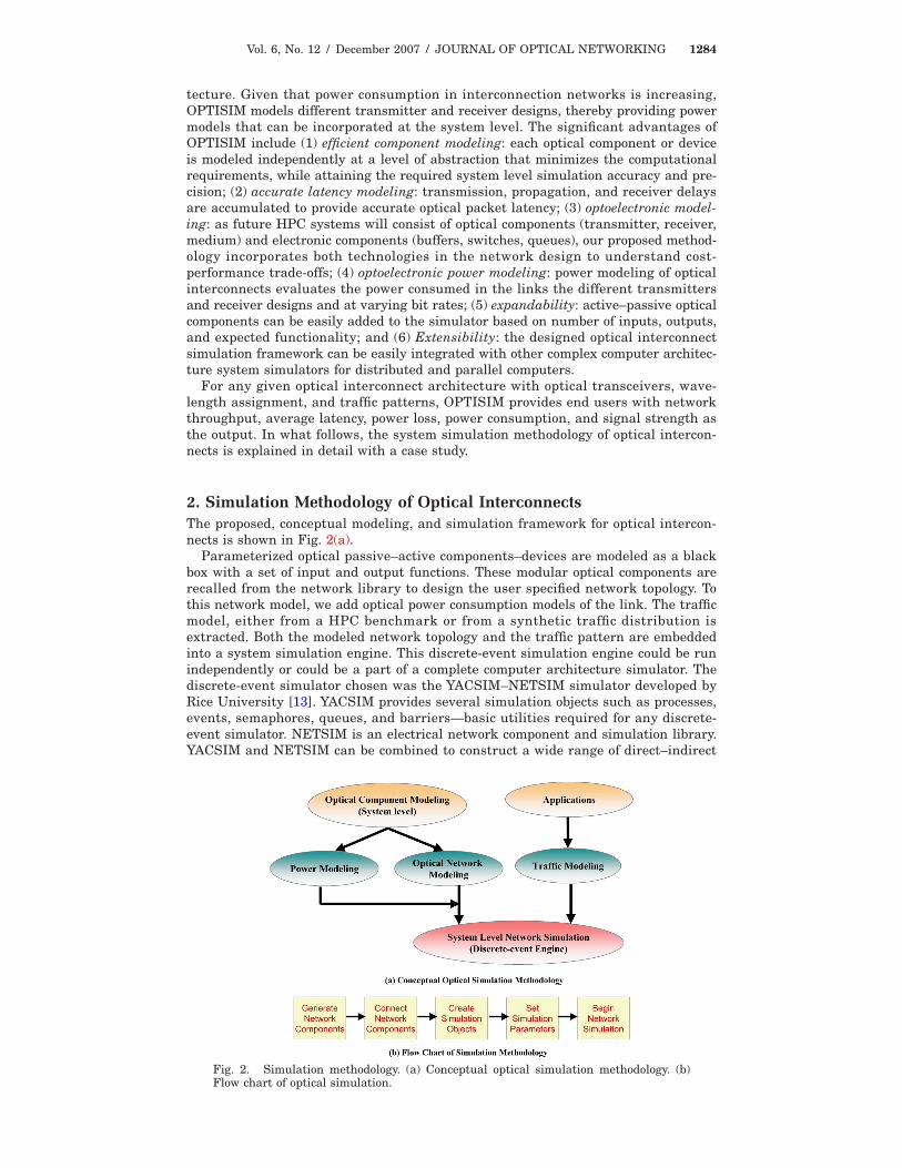
2. Simulation Methodology of Optical InterconnectsThe proposed, conceptual modeling, and simulation framework for optical intercon-nects is shown in Fig. 2(a).
Parameterized optical passive–active components–devices are modeled as a blackbox with a set of input and output functions. These modular optical components arerecalled from the network library to design the user specified network topology. Tothis network model, we add optical power consumption models of the link. The trafficmodel, either from a HPC benchmark or from a synthetic traffic distribution isextracted. Both the modeled network topology and the traffic pattern are embeddedinto a system simulation engine. This discrete-event simulation engine could be runindependently or could be a part of a complete computer architecture simulator. Thediscrete-event simulator chosen was the YACSIM–NETSIM simulator developed byRice University [13]. YACSIM provides several simulation objects such as processes,events, semaphores, queues, and barriers—basic utilities required for any discrete-event simulator. NETSIM is an electrical network component and simulation library.YACSIM and NETSIM can be combined to construct a wide range of direct–indirect
Fig. 2. Simulation methodology. (a) Conceptual optical simulation methodology. (b)Flow chart of optical simulation.
Vol. 6, No. 12 / December 2007 / JOURNAL OF OPTICAL NETWORKING 1285
electrical interconnects. Using YACSIM as the simulator engine, we augment theNETSIM library with optical components and optical simulation. We first explain thedesign of optical components and architecture, and then we explain the power modelsin our simulator.
2.A. Design of Optical Components and ArchitectureFrom Fig. 2(b), the first step in designing a system level optical interconnect-basedsimulator is to generate network components. NETSIM includes a library of severalelectrical components including ports (packets transmitting–receiving units), buffers(packet storage units), electronic routing units, and electronic switching units. TheNETSIM library is augmented with several active–passive optical components such aslasers, couplers, splitters, switches, wavelength converters, waveguides, fibers, multi-plexers, demultiplexers, and photodetectors. From the link–functional modeling ofeach of these components, four relevant parameters are extracted for the system levelmodeling: (1) length—to determine the propagation latency through the component,(2) attenuation—to determine the signal loss due to component, (3) wavelength—todetermine the routing within a component, and (4) power—to determine the powerconsumed by the component. Each optical component is designed with a set of inputparameters, Opticalcomponent�fanin, fanout, length, attenuation, wavelengths, power�,where fanin provides the number of inputs to the component, fanout provides thenumber of outputs from the component, length parameter specifies the length inmeters, attenuation refers to the signal loss in decibels due to the component, wave-lengths specifies the number of channels the component can transmit, and power cal-culates the power consumed due to the component. In certain optical components suchas wavelength converters, output wavelength will be a function of the received inputwavelength. The power consumed is calculated based on the type of optical componentspecified. This value is added only for active optical components such as transmitters,receivers, and other electro-optic devices.
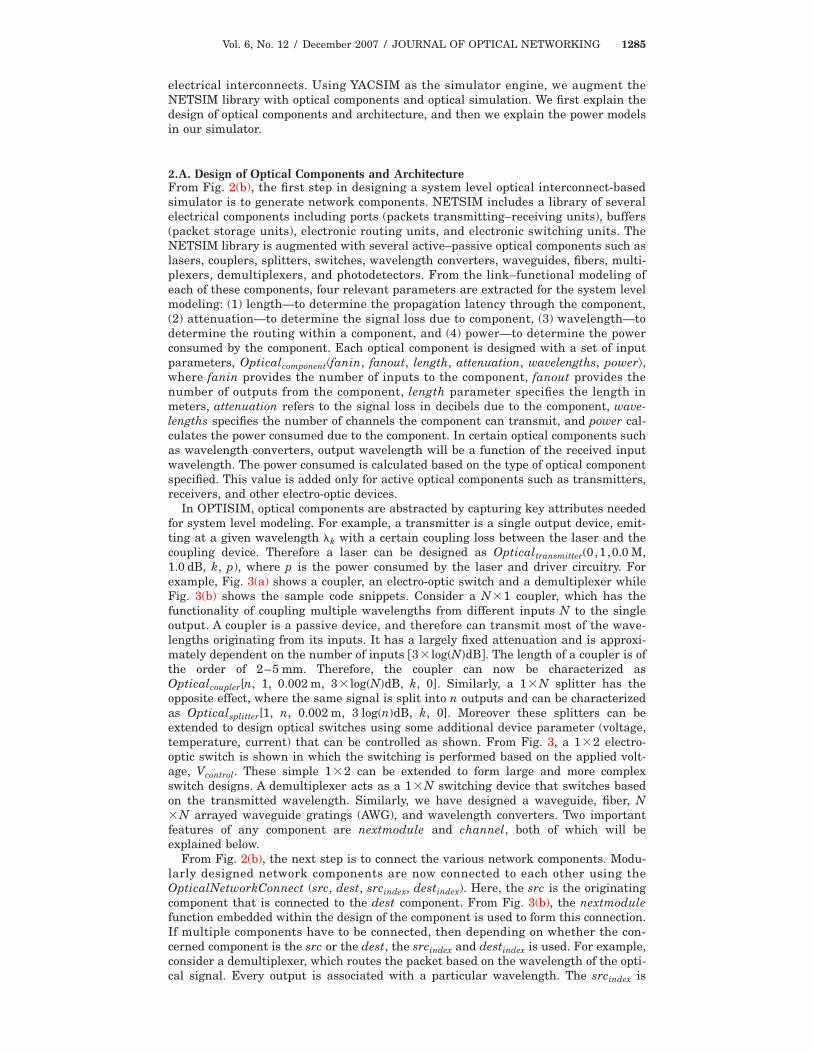
In OPTISIM, optical components are abstracted by capturing key attributes neededfor system level modeling. For example, a transmitter is a single output device, emit-ting at a given wavelength �k with a certain coupling loss between the laser and thecoupling device. Therefore a laser can be designed as Opticaltransmitter(0 ,1,0.0 M,1.0 dB, k, p), where p is the power consumed by the laser and driver circuitry. Forexample, Fig. 3(a) shows a coupler, an electro-optic switch and a demultiplexer whileFig. 3(b) shows the sample code snippets. Consider a N�1 coupler, which has thefunctionality of coupling multiple wavelengths from different inputs N to the singleoutput. A coupler is a passive device, and therefore can transmit most of the wave-lengths originating from its inputs. It has a largely fixed attenuation and is approxi-mately dependent on the number of inputs �3� log�N�dB�. The length of a coupler is ofthe order of 2–5 mm. Therefore, the coupler can now be characterized asOpticalcoupler[n, 1, 0.002 m, 3� log�N�dB, k, 0]. Similarly, a 1�N splitter has theopposite effect, where the same signal is split into n outputs and can be characterizedas Opticalsplitter[1, n, 0.002 m, 3 log�n�dB, k, 0]. Moreover these splitters can beextended to design optical switches using some additional device parameter (voltage,temperature, current) that can be controlled as shown. From Fig. 3, a 1�2 electro-optic switch is shown in which the switching is performed based on the applied volt-age, Vcontrol. These simple 1�2 can be extended to form large and more complexswitch designs. A demultiplexer acts as a 1�N switching device that switches basedon the transmitted wavelength. Similarly, we have designed a waveguide, fiber, N�N arrayed waveguide gratings (AWG), and wavelength converters. Two importantfeatures of any component are nextmodule and channel, both of which will beexplained below.
From Fig. 2(b), the next step is to connect the various network components. Modu-larly designed network components are now connected to each other using theOpticalNetworkConnect (src, dest, srcindex, destindex). Here, the src is the originatingcomponent that is connected to the dest component. From Fig. 3(b), the nextmodulefunction embedded within the design of the component is used to form this connection.If multiple components have to be connected, then depending on whether the con-cerned component is the src or the dest, the srcindex and destindex is used. For example,consider a demultiplexer, which routes the packet based on the wavelength of the opti-cal signal. Every output is associated with a particular wavelength. The src is
index
Vol. 6, No. 12 / December 2007 / JOURNAL OF OPTICAL NETWORKING 1286
used to indicate the correct next module the demultiplexer’s output should be con-nected to. The third step from Fig. 2(b), is to create simulation objects, and the fourthstep is to set the simulation parameters, both of which are accomplished by using theYACSIM engine.
2.B. Optical Packet SimulationEach packet is generated with a unique sequence number in the system. In OPTISIM,an optical packet is simulated by using two events (procedures), one is called the headevent and the other is called the tail event. Every time an optical packet is ready to beinjected into the network, the two events are automatically generated. The opticalpacket is injected into the network with some attributes, such as signal strength ofthe laser and the wavelength associated with the transmitter port. The head eventimmediately sets the path from the source to the destination. Consider Fig. 4, whichdescribes the optical packet simulation methodology.
This consists of four tunable transmitters and four fixed receivers. Each transmit-ter is associated with multiple wavelengths (an array of lasers) so that it can reachany of the receivers. Consider the packet transmission from transmitter (Tx 0) toreceiver (Rx 1) on wavelength �0 as shown in Fig. 4(a). The head identified as H usesthe nextmodule function embedded in each component to trace to the next component.The head from Tx 0 traces the route through coupler 1, coupler 2, demultiplexer,waveguide, and receiver. At each component, the head event accrues severalattributes of the component, such as length of the component, attenuation due to thecomponent, and routing due to the component. In addition, the head of the packetembeds the packet sequence number into the channel specified by the component.When the head of the packet from Tx 0 reaches the coupler 2, the head event firstchecks, and then embeds the sequence number (1200) of the packet into channel �0associated with the component. Additional features embedded into the functionality ofthe component are executed when the head reaches the particular component. Forexample, consider a splitter that splits the input signal into all its outputs. Here, thehead event needs to re-create multiple instances of the packets with similar attributes
Fig. 3. Modular approach of designing optical components. (a) Example optical compo-nents shown include a coupler, a demultiplexer, and a fiber. (b) Example code for gen-erating these components.

Vol. 6, No. 12 / December 2007 / JOURNAL OF OPTICAL NETWORKING 1287
and restart the simulation for each of the newly generated packets. Once, the headevent reaches the receiver port, it is terminated.
After the tail event is created and identified as T, it is immediately delayed for thetransmission latency and held in the transmitter port. The transmission latency is
Fig. 4. Simulation example. (a) Tx 0 transmits the packet, the head reaches the Rx 1embedding the sequence numbers (1200) within each component of the network. (b)Other transmitters Tx 1, Tx 2, and Tx 3 transmit the packets. The mid flits from Tx 0have now reached the receiver. (c) The tail flit from Tx 0 removes the embedding, andthe mid flits from Tx 1, Tx 2, and Tx 3 have reached the receiver.
Vol. 6, No. 12 / December 2007 / JOURNAL OF OPTICAL NETWORKING 1288
obtained by dividing the packet size (in bits) with the bit rate of the transmitter.Figure 4(b) shows the mid flits, identified as M (flit is the smallest unit of packettransmission, generally consisting of a several bits) of the packet transmitted by Tx 0having reached the receiver. In addition, other head events from transmitters Tx 1, Tx2, and Tx 3 have reached their respective receivers. The tail event then retraces thesame path as the head of the optical packet, and further delays for the propagationlatency. The tail event checks each component that it traces whether the packet’ssequence number exists. If the sequence number exists at the correct wavelength,then the tail erases the sequence number, thereby tears down the path as shown inFig. 3(c) for Tx 0. This embedding of the sequence number enhances the validity of theproposed model. Moreover, once it reaches the receiver port, it delays for receiverlatency in detecting the packet.
2.C. Power Modeling of Optical InterconnectsPower consumption of an optical link is becoming as critical as its speed [11] in HPCsystem design. In this subsection, we provide an analytical framework to capturepower consumption that can be incorporated into the system modeling design throughpower configuration files. An optical link consists of the transmitter, the receiver, andthe channel. Considering a passive channel, the total power consumption of an opticallink depends on the transmitter and the receiver power. Transmitter power is con-sumed at the laser, and laser driver–modulator, whereas the receiver power is con-sumed at the photodetector, transimpedance amplifier (TIA), and clock and datarecovery (CDR) circuitry [11,14]. Multiple-quantum wells (MQWs) [14] with externalmodulators and vertical-cavity surface-emitting lasers (VCSELs) [14] are suitablecandidates for laser sources. MQW needs an external laser source to generate light,where as for VCSEL the light is generated on-chip itself. For the receiver, two designsare incorporated, low-impedance resistive receiver and TIA-based receiver design.Below, we evaluate the power dissipated in an optoelectronic link based on differenttransmitters and receiver designs. The total power consumed by an entire optoelec-tronic link is given by
PT = PTX + PRX = �Pdriver + Plaser�TX
+ �Pphotodiode + PTIA + PCDR�RX. �1�
The superbuffer in the laser driver is a set of cascaded inverters, and the size ofeach inverter is larger than the previous one by a constant factor �. This superbufferstage will be used for both the MQW- and VCSEL-based designs [14]. The total powerdissipated in the driver stages is calculated as
Pdriver = �CLVdd2 BR, �2�
where � is the switching factor, CL is the total load capacitance of the superbuffers (ofn inverters), Vdd is the supply voltage, and BR is the bit rate. The total capacitance isthe sum of input and output capacitance of all the inverters, and is given as [14]
CL = Cload − Cin + �k=0
n−1
�Cin + Cout��k, �3�
where Cload is the load capacitance of the inverter chain, and Cin and Cout are theinput and output capacitances of the minimum sized inverters.
In MQW-based modulators, light is received from the external mode-locked laser.The modulator performance is characterized by its contrast ratio (CR), insertion loss(IL) at its optimal bias voltage �Vbias�, and the voltage swing required �V0. The powerdissipated in the modulator is given as [15]
PMQW =Pl
�link
q
h��Vbias�1 + IL −
1 − IL
CR − �V0IL , �4�
where Pl is the average optical power required at the receiver input, and �link is theoptical system efficiency. For a VCSEL-based system, we adopt a complementarymetal-oxide semiconductor (CMOS) driver design from [14], where the driver circuitryconsists of two n-type metal-oxide semiconductor (NMOS) transistors providing thethreshold and modulation currents and a superbuffer driving the gate that delivers
Vol. 6, No. 12 / December 2007 / JOURNAL OF OPTICAL NETWORKING 1289
the modulation current. The VCSEL power consumed is given as [14]
PVCSEL = ItotalVsource = �Ith + Im���Vth + ImRs + Vdd − Vtn�. �5�
The total current is the sum of threshold �Ith� and modulation currents times theswitching factor. The total voltage is the sum of the VCSEL threshold voltage �Vth�,the voltage drop across the series resistance �Rs�, and the minimum source-drain volt-age �Vdd−Vtn� to ensure the gate that delivers the modulation current is in saturation.
For the TIA-based receiver design, we determine the power consumed by the photo-detector and the TIA. This is modeled similar to [16], which consists of the photode-tector as a current source �Id+�Im� and a common source amplifier connected by afeedback resistance, Rf. Id is the dark current, � is the VCSEL efficiency in A/W, and is the detector efficiency in W/A. The input capacitance to the amplifier Cin=CD+Cg, where CD is the diode capacitance and Cg=CoxWL is the gate capacitance. TheVCSEL needs to generate enough light that depends on Im such that the receiver willproduce an output signal of amplitude �V0, which can then be amplified by furtherreceiver stages. This can be approximated as [16]
�V0 =�Im
�Rf. �6�
Therefore, the power consumption of the VCSEL is defined by the needs of thereceiver for a given BR and Vdd. The total power dissipated in the TIA-based receivercircuit is then given as
PTIA = IbVdd + Id2Vdd + ���Im�2Rf, �7�
where Ib is the bias current of the internal amplifier and is given by Ib=3 db intVeC0where 3 db int is the 3 db bandwidth of the internal amplifier, Ve is the early voltage,and C0 is the output capacitance. The gain-bandwidth (GBW) product of the internalamplifier is GBW=A��3 db int=gm /C0, where w=2�BR, and gm is the transconduc-tance. The relationship between the internal amplifier bandwidth and the maximumbit rate is given as =0.353 db int. The bandwidth of TIA is assumed to be half thebandwidth of the internal amplifier, therefore, the 3 dB bandwidth of TIA is approxi-mated as
3 db TIA =A��
RfCin=
w
0.7. �8�
Then the total power dissipated at the receiver can be obtained as
PTIA =0.7A��Id
2
2�CinBR+ �2�VeC0Vdd
0.35+
2���V02Cin
0.7A�� BR. �9�
Then the desired Im at the transmitter can be obtained by solving Eqs. (5), (7), and (8).For the low-impedance resistive receiver link design, the total receiver power con-
sumption is given as [16]
PRC = VddId +�Vdd�V0�CLBR
�0.7, �10�
where CL is the load capacitance on the RC receiver composed of the photodetectorcapacitance and the capacitance of the next stage. The power dissipated at the CDRunit is given as [11]
PCDR = �CCDRVdd2 BR, �11�
where CCDR is the capacitance of the CDR unit. We have modeled two transmitterdesigns, VCSEL and MQW, and two receiver designs, resistive and TIA receivers.These transmitters and receivers can be incorporated into the link design to capturethe power consumption of the designed optoelectronic link.
Vol. 6, No. 12 / December 2007 / JOURNAL OF OPTICAL NETWORKING 1290
3. OPTISIM: Parameter Extraction and System SimulationTo explain the working of the simulator, it is necessary to validate the simulationmethodology by comparing our approach to a real machine employing optical intercon-nects. However, given the difficulties in testing a real machine [17] and the limitedscope of this research, we have adopted a different approach of extracting parametersfrom well-known simulation tools (OptiBPM and Optisystem) from Optiwave Corpora-tion and plugging these into our proposed system simulator.
We designed various optical components–devices using different materials to obtainthe desired refractive index contrast, output signal amplitude, and wave propagationusing the device level simulator (OptiBPM). These discrete components were thenplugged into the link level simulator (OptiSystem) to ensure that the eye opening,BER, receiver power and signal amplitude were sufficient at the specified bit ratesand frequency. In addition, we also modeled the power dissipated by the devices andcalculated the power consumed by an electro-optic link. This permitted us to test andto some extent validate the proposed simulation methodology. Then the values (power,attenuation, length, and other parameters) obtained from OptiSystem were pluggedinto our proposed system level simulation (OPTISIM). Then to explain the results(throughput, latency) that can be obtained using the simulator, we show with a casestudy of an optical interconnect-based system architecture.
The following subsections are explained as follows. In Subsection 3.A the device–component study performed using OptiBPM is explained. Then, in Subsection 3.B thelink level simulation for a four-channel (wavelengths) using the parameters extractedfrom OptiBPM is explained using the OptiSystem tool. In Subsection 3.C, at the linklevel, we also explain the power consumed by a single channel and how to modelMQW and VCSEL lasers. Finally, in Subsection 3.D we show with a case study, how tomodel an optical interconnect and the results obtained.
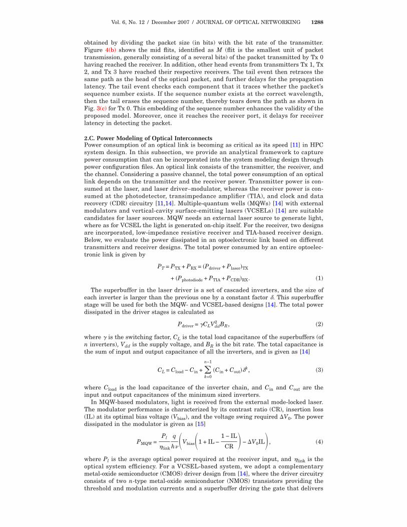
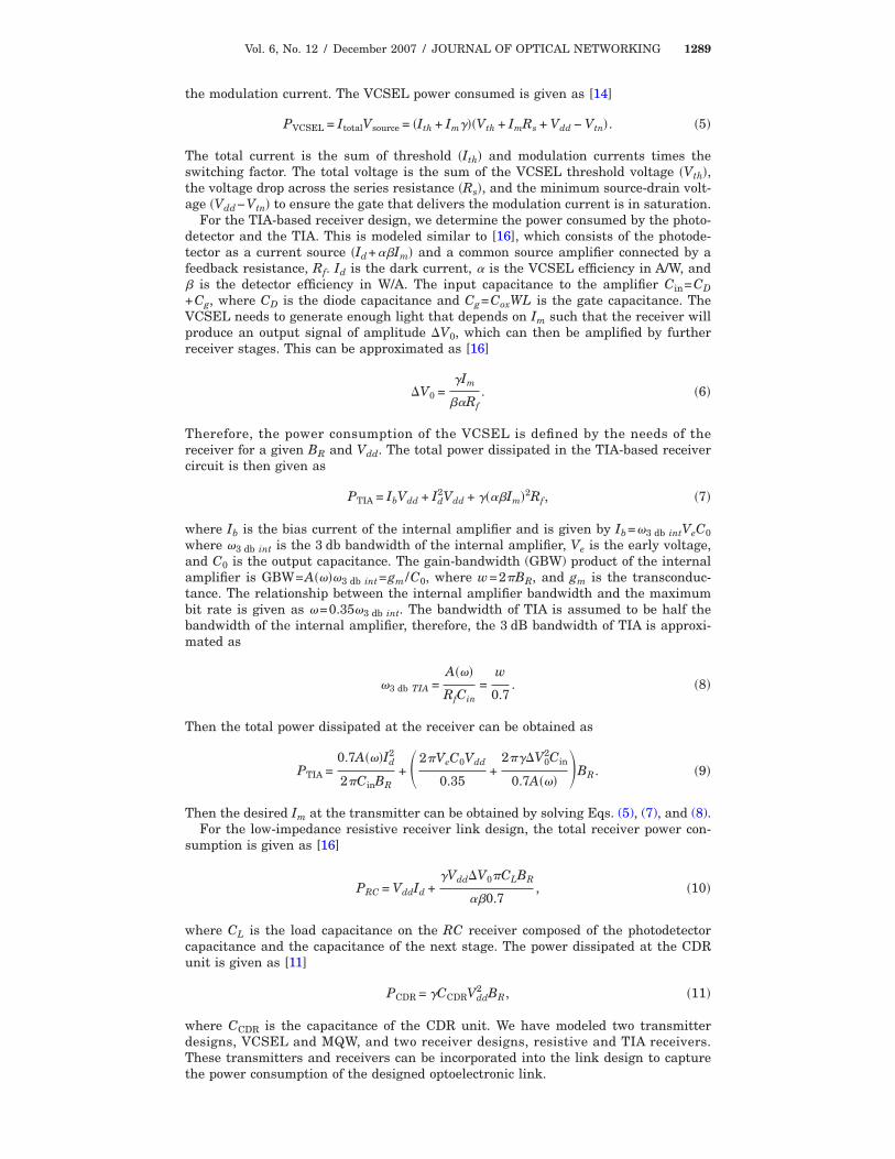
3.A. OptiBPM ModelingWe modeled a 3 dB coupler that was designed using a substrate with cladding refrac-tive index, nc of 1.442 and core refractive index, nr of 1.5. The output of this wafersimulation is shown in Fig. 5(a). The device length was 0.8 mm and the output signalhad an intensity of 0.45 (3.3 dB attenuation). Similarly a 1�4 splitter was also mod-eled as shown in Fig. 5(b). The length of the splitter was 1.4 mm and the receivedintensity at the output was measured to be 0.24 implying a 6 dB attenuation. Usingthe WDM phasar, we evaluated the length of the demultiplexer to be 1.9 mm and anattenuation of 2.1 dB. These parameters were included in the definition files for theOPTISIM simulation library. Currently, we have couplers, splitters, electro-opticswitches, wavelength converters, demultiplexers, multiplexers, waveguides, and fibersin our simulator.
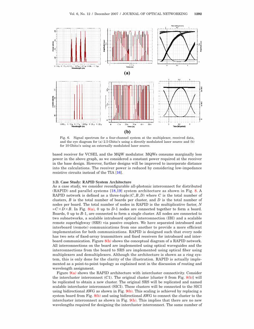
3.B. OptiSystem ModelingThe OptiBPM parameters obtained were then simulated using the OptiSystem simu-lation tool for a four-channel optical interconnect-based architecture. The directlymodulated laser for four channels was solved using rate equations at data rate of2.5 Gbits/s. The lazing channels were 1116.2, 1116.9, 1117.6, and 1118.3 nm; thewavelength spacing being 0.7 nm. The input power to the laser was 2 mW or 0.3 dBm.The losses seen by the signal include propagation loss of 0.2 dB/km, multiplexer lossof 3 dB per stage, and demultiplexer loss of 2.1 dB. Figure 6(a) shows the multiplexedspectrum, the received signal and eye diagram at 2.5 Gbits/s. The eye diagram showsthe eye height of 1.39�10−5, threshold of 9�10−7, and a low BER. Figure 6(b) showsthe optical interconnect performance for a four-channel system with CW laser and anexternal Mach–Zehneder modulator at 10 Gbits/s. The eye diagram shows the eyeheight of 2.21�10−5, threshold of 2.89�10−6 and a low BER. This clearly shows thatthe four-channel system designed using OptiSystem performs within accepted BERand power budget.
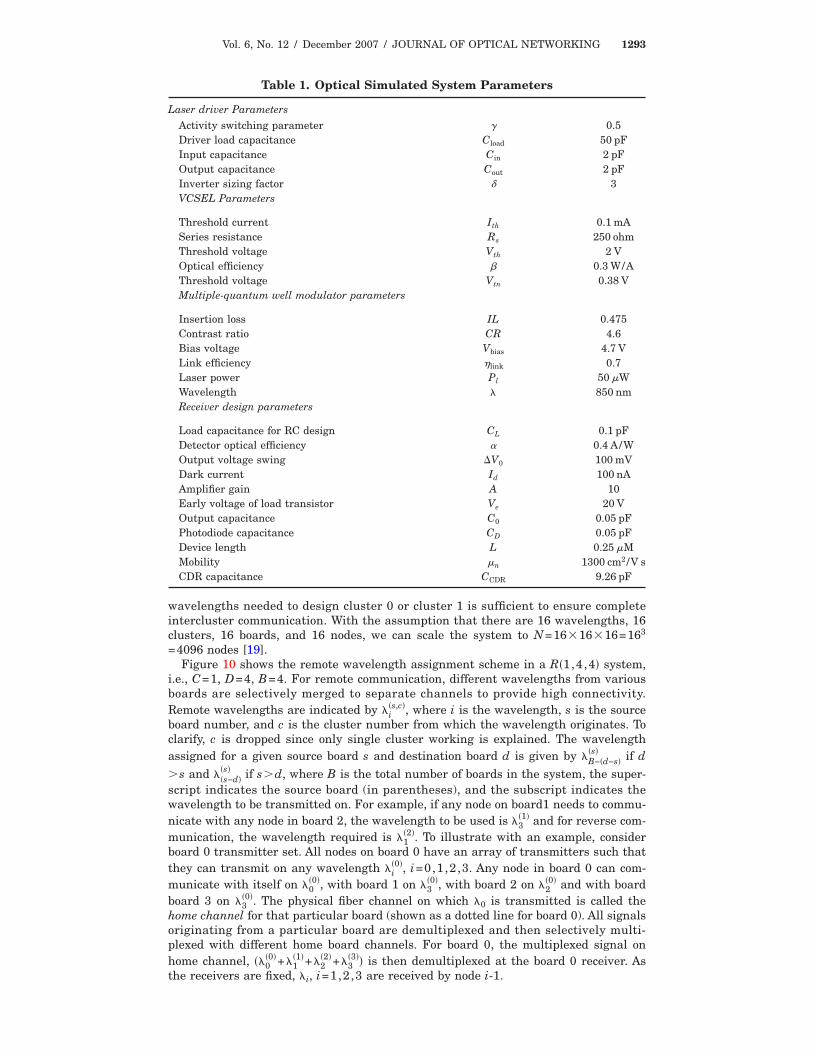
3.C. Power EstimationsThe parameters for VCSEL and MQW modulators were extracted from [14–16].Table 1 shows various parameters of the laser driver module, VCSEL, MQWs, and thereceiver design parameters.
Vol. 6, No. 12 / December 2007 / JOURNAL OF OPTICAL NETWORKING 1291
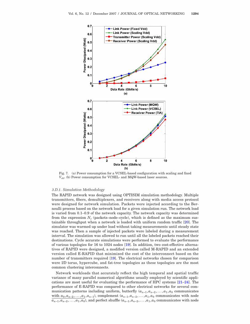
From the parameters shown in Table 1 and solving equations from Subsection 2.C,we estimated the power dissipated at the transmitter and the receiver at varying bitrates. The link power is dominated by the receiver power consisting of the TIA andCDR whereas the laser and driver dissipate minimal power. Figure 7(a) shows thelink power for VCSEL-based configuration with fixed Vdd, where the supply voltage isnot varied, scaling Vdd, where the supply voltage is scaled with the bit rates, trans-mitter power with scaled Vdd and receiver power with scaled Vdd. With scaling of bitrates and supply voltages, the power dissipated in a VCSEL is dominated by thereceiver consisting of TIA and CDR. The total power dissipated at 10 Gbits/s isapproximately 535 mW. With the bit rate scaling from 10 to 5 Gbits/s and the supplyvoltage scaling from 1.8 to 0.9 V, the power dissipation for a 5 Gbits/s link reduces toalmost 108 mW. Figure 7(b) shows the power dissipated at varying bit rates for TIA-
Fig. 5. (a) Output from a 3 dB coupler and (b) 1�4 splitter.
Vol. 6, No. 12 / December 2007 / JOURNAL OF OPTICAL NETWORKING 1292
based receiver for VCSEL and the MQW modulator. MQWs consume marginally lesspower in the above graph, as we considered a constant power required at the receiverin the base design. However, further designs will be improved to incorporate distanceinto the calculations. The receiver power is reduced by considering low-impedanceresistive circuits instead of the TIA [16].
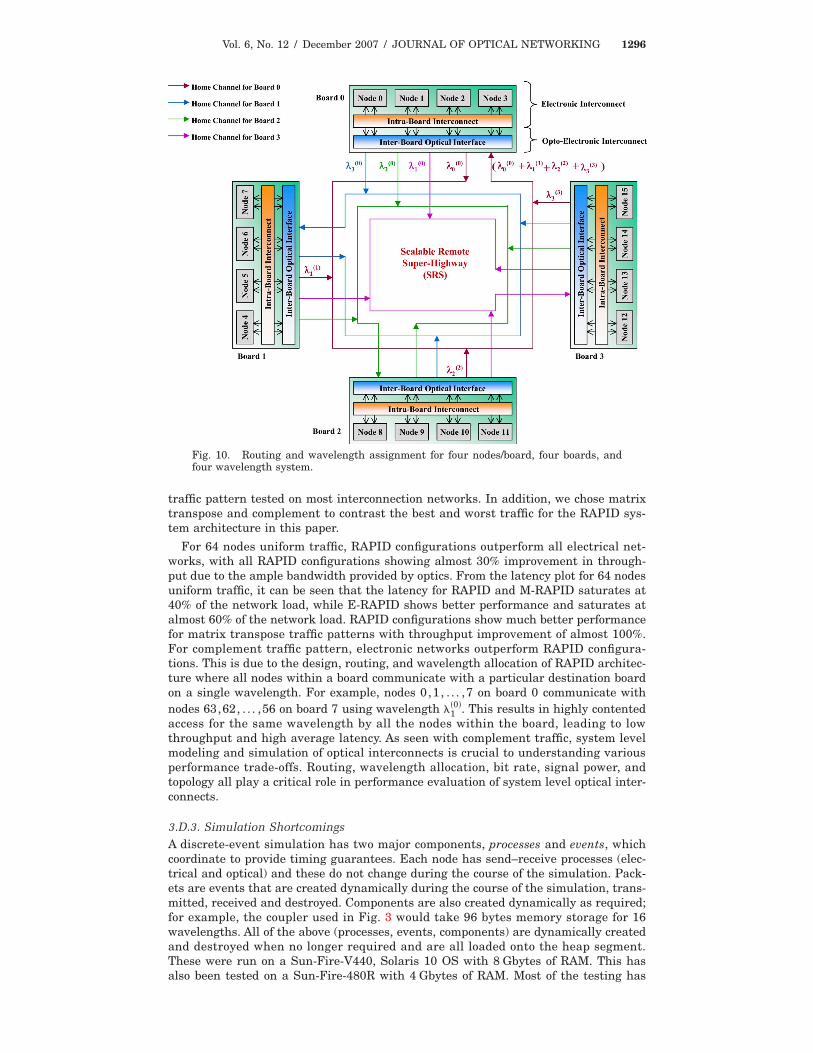
3.D. Case Study: RAPID System ArchitectureAs a case study, we consider reconfigurable all-photonic interconnect for distributed(RAPID) and parallel systems [18,19] system architecture as shown in Fig. 8. ARAPID network is defined as a three-tuple:�C ,B ,D� where C is the total number ofclusters, B is the total number of boards per cluster, and D is the total number ofnodes per board. The total number of nodes in RAPID is the multiplicative factor, N=C�D�B. In Fig. 8(a), 0 up to D-1 nodes are connected together to form a board.Boards, 0 up to B-1, are connected to form a single cluster. All nodes are connected totwo subnetworks, a scalable intraboard optical interconnection (IBI) and a scalableremote superhighway (SRS) via passive couplers. We have separated intraboard andinterboard (remote) communications from one another to provide a more efficientimplementation for both communications. RAPID is designed such that every nodehas two sets of fixed-array transmitters and fixed receivers for intraboard and inter-board communication. Figure 8(b) shows the conceptual diagram of a RAPID network.All interconnections on the board are implemented using optical waveguides and theinterconnections from the board to SRS are implemented using optical fiber usingmultiplexers and demultiplexers. Although the architecture is shown as a ring sys-tem, this is only done for the clarity of the illustration. RAPID is actually imple-mented as a point-to-point topology as explained next in the discussion of routing andwavelength assignment.
Figure 9(a) shows the RAPID architecture with intercluster connectivity. Considerthe intercluster interconnect �C1�. The original cluster [cluster 0 from Fig. 8(b)] willbe replicated to obtain a new cluster. The original SRS will be replicated and namedscalable intercluster interconnect (SICI). These clusters will be connected to the SICIusing bidirectional AWG as shown in Fig. 9(b). This scaling is achieved by replacing asystem board from Fig. 8(b) and using bidirectional AWG to connect the cluster to theintercluster interconnect as shown in Fig. 9(b). This implies that there are no newwavelengths required for designing the intercluster interconnect. The same number of
Fig. 6. Signal spectrum for a four-channel system at the multiplexer, received data,and the eye diagram for (a) 2.5 Gbits/s using a directly modulated laser source and (b)for 10 Gbits/s using an externally modulated laser source.
Vol. 6, No. 12 / December 2007 / JOURNAL OF OPTICAL NETWORKING 1293
wavelengths needed to design cluster 0 or cluster 1 is sufficient to ensure completeintercluster communication. With the assumption that there are 16 wavelengths, 16clusters, 16 boards, and 16 nodes, we can scale the system to N=16�16�16=163
=4096 nodes [19].Figure 10 shows the remote wavelength assignment scheme in a R�1,4,4� system,
i.e., C=1, D=4, B=4. For remote communication, different wavelengths from variousboards are selectively merged to separate channels to provide high connectivity.Remote wavelengths are indicated by �i
�s,c�, where i is the wavelength, s is the sourceboard number, and c is the cluster number from which the wavelength originates. Toclarify, c is dropped since only single cluster working is explained. The wavelengthassigned for a given source board s and destination board d is given by �B−�d−s�
�s� if d
�s and ��s−d��s� if s�d, where B is the total number of boards in the system, the super-
script indicates the source board (in parentheses), and the subscript indicates thewavelength to be transmitted on. For example, if any node on board1 needs to commu-nicate with any node in board 2, the wavelength to be used is �3
�1� and for reverse com-munication, the wavelength required is �1
�2�. To illustrate with an example, considerboard 0 transmitter set. All nodes on board 0 have an array of transmitters such thatthey can transmit on any wavelength �i
�0�, i=0,1,2,3. Any node in board 0 can com-municate with itself on �0
�0�, with board 1 on �3�0�, with board 2 on �2
�0� and with boardboard 3 on �3
�0�. The physical fiber channel on which �0 is transmitted is called thehome channel for that particular board (shown as a dotted line for board 0). All signalsoriginating from a particular board are demultiplexed and then selectively multi-plexed with different home board channels. For board 0, the multiplexed signal onhome channel, ��0
�0�+�1�1�+�2
�2�+�3�3�� is then demultiplexed at the board 0 receiver. As
the receivers are fixed, � , i=1,2,3 are received by node i-1.
Table 1. Optical Simulated System Parameters
Laser driver ParametersActivity switching parameter � 0.5Driver load capacitance Cload 50 pFInput capacitance Cin 2 pFOutput capacitance Cout 2 pFInverter sizing factor � 3VCSEL Parameters
Threshold current Ith 0.1 mASeries resistance Rs 250 ohmThreshold voltage Vth 2 VOptical efficiency 0.3 W/AThreshold voltage Vtn 0.38 VMultiple-quantum well modulator parameters
Insertion loss IL 0.475Contrast ratio CR 4.6Bias voltage Vbias 4.7 VLink efficiency �link 0.7Laser power Pl 50 WWavelength � 850 nmReceiver design parameters
Load capacitance for RC design CL 0.1 pFDetector optical efficiency � 0.4 A/WOutput voltage swing �V0 100 mVDark current Id 100 nAAmplifier gain A 10Early voltage of load transistor Ve 20 VOutput capacitance C0 0.05 pFPhotodiode capacitance CD 0.05 pFDevice length L 0.25 MMobility n 1300 cm2/V sCDR capacitance CCDR 9.26 pF
i
Vol. 6, No. 12 / December 2007 / JOURNAL OF OPTICAL NETWORKING 1294
3.D.1. Simulation MethodologyThe RAPID network was designed using OPTISIM simulation methodology. Multipletransmitters, fibers, demultiplexers, and receivers along with media access protocolwere designed for network simulation. Packets were injected according to the Ber-noulli process based on the network load for a given simulation run. The network loadis varied from 0.1–0.9 of the network capacity. The network capacity was determinedfrom the expression Nc (packets–node–cycle), which is defined as the maximum sus-tainable throughput when a network is loaded with uniform random traffic [20]. Thesimulator was warmed up under load without taking measurements until steady statewas reached. Then a sample of injected packets were labeled during a measurementinterval. The simulation was allowed to run until all the labeled packets reached theirdestinations. Cycle accurate simulations were performed to evaluate the performanceof various topologies for 16 to 1024 nodes [19]. In addition, two cost-effective alterna-tives of RAPID were designed, a modified version called M-RAPID and an extendedversion called E-RAPID that minimized the cost of the interconnect based on thenumber of transmitters required [19]. The electrical networks chosen for comparisonwere 2D torus, hypercube, and fat-tree topologies as these topologies are the mostcommon clustering interconnects.
Network workloads that accurately reflect the high temporal and spatial trafficvariance of many parallel numerical algorithms usually employed by scientific appli-cations are most useful for evaluating the performance of HPC systems [21–24]. Theperformance of E-RAPID was compared to other electrical networks for several com-munication patterns including uniform, butterfly (an−1,an−2, . . . ,a1 ,a0 communicateswith a0 ,an−2, . . . ,a1 ,an−1), complement (an−1,an−2, . . . ,a1 ,a0 communicates with nodea ,a , . . . ,a ,a ), and perfect shuffle (a ,a , . . . ,a ,a communicates with node
Fig. 7. (a) Power consumption for a VCSEL-based configuration with scaling and fixedVdd. (b) Power consumption for VCSEL- and MQW-based laser sources.
n−1 n−2 1 0 n−1 n−2 1 0

Vol. 6, No. 12 / December 2007 / JOURNAL OF OPTICAL NETWORKING 1295
an−2,an−3, . . . ,a0 ,an−1) for a network size of 64 nodes. While traditional HPC applica-tions will employ these traffic patterns in various phases for communication, by sepa-rately testing these traffic patterns, it will be possible to identify the best- and worst-case traffic patterns for a given network topology [20,23].
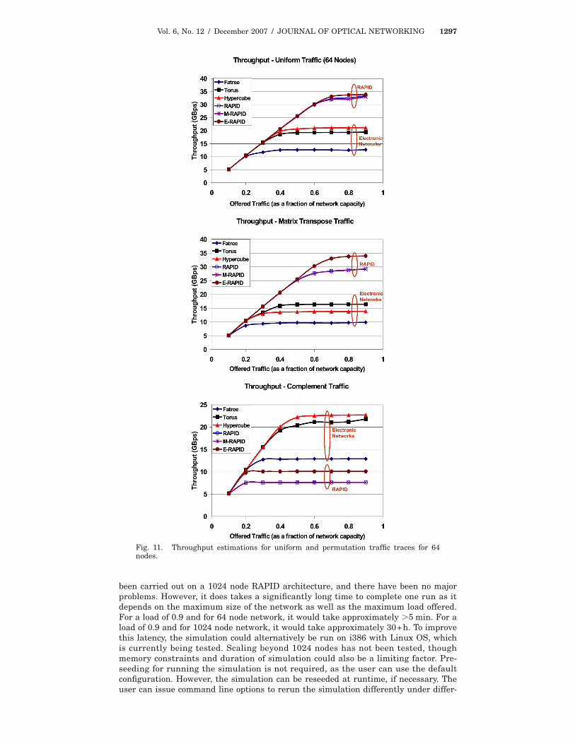
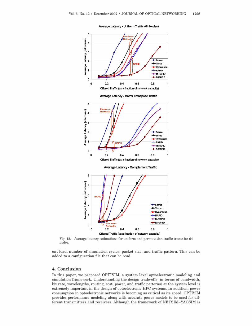
3.D.2. Simulation ResultsFigures 11 and 12 show the throughput and latency for a subset of traffic patterns;namely, uniform, matrix transpose, and complement. Uniform is the most common
Fig. 8. Architectural overview of RAPID. Every node is connected to two scalable in-terconnects: an optical intraboard interconnect and a SRS.
Fig. 9. Scalability of RAPID architecture. (a) Multiple clusters are connected to scal-able intercluster interconnect (SICI). (b) Intercluster interconnect implementation us-ing bidirectional AWG.
Vol. 6, No. 12 / December 2007 / JOURNAL OF OPTICAL NETWORKING 1296
traffic pattern tested on most interconnection networks. In addition, we chose matrixtranspose and complement to contrast the best and worst traffic for the RAPID sys-tem architecture in this paper.
For 64 nodes uniform traffic, RAPID configurations outperform all electrical net-works, with all RAPID configurations showing almost 30% improvement in through-put due to the ample bandwidth provided by optics. From the latency plot for 64 nodesuniform traffic, it can be seen that the latency for RAPID and M-RAPID saturates at40% of the network load, while E-RAPID shows better performance and saturates atalmost 60% of the network load. RAPID configurations show much better performancefor matrix transpose traffic patterns with throughput improvement of almost 100%.For complement traffic pattern, electronic networks outperform RAPID configura-tions. This is due to the design, routing, and wavelength allocation of RAPID architec-ture where all nodes within a board communicate with a particular destination boardon a single wavelength. For example, nodes 0,1, . . . ,7 on board 0 communicate withnodes 63,62, . . . ,56 on board 7 using wavelength �1
�0�. This results in highly contentedaccess for the same wavelength by all the nodes within the board, leading to lowthroughput and high average latency. As seen with complement traffic, system levelmodeling and simulation of optical interconnects is crucial to understanding variousperformance trade-offs. Routing, wavelength allocation, bit rate, signal power, andtopology all play a critical role in performance evaluation of system level optical inter-connects.
3.D.3. Simulation ShortcomingsA discrete-event simulation has two major components, processes and events, whichcoordinate to provide timing guarantees. Each node has send–receive processes (elec-trical and optical) and these do not change during the course of the simulation. Pack-ets are events that are created dynamically during the course of the simulation, trans-mitted, received and destroyed. Components are also created dynamically as required;for example, the coupler used in Fig. 3 would take 96 bytes memory storage for 16wavelengths. All of the above (processes, events, components) are dynamically createdand destroyed when no longer required and are all loaded onto the heap segment.These were run on a Sun-Fire-V440, Solaris 10 OS with 8 Gbytes of RAM. This hasalso been tested on a Sun-Fire-480R with 4 Gbytes of RAM. Most of the testing has
Fig. 10. Routing and wavelength assignment for four nodes/board, four boards, andfour wavelength system.
Vol. 6, No. 12 / December 2007 / JOURNAL OF OPTICAL NETWORKING 1297
been carried out on a 1024 node RAPID architecture, and there have been no majorproblems. However, it does takes a significantly long time to complete one run as itdepends on the maximum size of the network as well as the maximum load offered.For a load of 0.9 and for 64 node network, it would take approximately �5 min. For aload of 0.9 and for 1024 node network, it would take approximately 30+h. To improvethis latency, the simulation could alternatively be run on i386 with Linux OS, whichis currently being tested. Scaling beyond 1024 nodes has not been tested, thoughmemory constraints and duration of simulation could also be a limiting factor. Pre-seeding for running the simulation is not required, as the user can use the defaultconfiguration. However, the simulation can be reseeded at runtime, if necessary. Theuser can issue command line options to rerun the simulation differently under differ-
Fig. 11. Throughput estimations for uniform and permutation traffic traces for 64nodes.
Vol. 6, No. 12 / December 2007 / JOURNAL OF OPTICAL NETWORKING 1298
ent load, number of simulation cycles, packet size, and traffic pattern. This can beadded to a configuration file that can be read.
4. ConclusionIn this paper, we proposed OPTISIM, a system level optoelectronic modeling andsimulation framework. Understanding the design trade-offs (in terms of bandwidth,bit rate, wavelengths, routing, cost, power, and traffic patterns) at the system level isextremely important in the design of optoelectronic HPC systems. In addition, powerconsumption in optoelectronic networks is becoming as critical as its speed. OPTISIMprovides performance modeling along with accurate power models to be used for dif-ferent transmitters and receivers. Although the framework of NETSIM–YACSIM is
Fig. 12. Average latency estimations for uniform and permutation traffic traces for 64nodes.

Vol. 6, No. 12 / December 2007 / JOURNAL OF OPTICAL NETWORKING 1299
used, it has been modified extensively by enhancing the component design space,extending the network design space, and modifying the simulation design space. A dis-crete event simulation environment combined with component–device modeling pro-vides an attractive avenue for analyzing the power-performance trade-offs in HPCsystems. Additionally, the proposed modeling and simulation methodology can easilybe integrated with other complete computer architecture tool sets such as the RiceSimulator for ILP Multiprocessors (RSIM) [25] to study architectural designtrade-offs.
We are currently in the process of creating a reference manual to simplify theunderstanding of the simulator. In addition, we are currently testing the RSIM simu-lator integrated with our OPTISIM to test HPC applications such as fast Fouriertransforms, LU, Ocean and other Splash-2 suites. Lastly, we want the simulator to beworking on even Linux systems in the near future. Once we have the OS compatibil-ity, architectural platform compatibility (RSIM), and the manual ready, we will dis-seminate this simulator through the web.
AcknowledgmentsThis research is supported by National Science Foundation (NSF) grants CCR-0538945 and ECCS-0725765.
References1. E. Mohammed, A. Alduino, T. Thomas, H. Braunisch, D. Lu, J. Heck, A. Liu, I. Young, B.
Barnett, G. Vandenton, and R. Mooney, “Optical interconnect system integration forultra-short reach applications,” Intel Technol. J. 8, 115–128 (2004).
2. A. F. Benner, M. Ignatowski, J. A. Kash, D. M. Kuchta, and M. B. Ritter, “Exploitation ofoptical interconnects in future server architectures,” IBM J. Res. Dev. 49, 755–775 (2005).
3. D. A. B. Miller, “Rationale and challenges for optical interconnects to electronic chips,” Proc.IEEE 88, 728–749 (2000).
4. J. H. Collet, D. Litaize, J. V. Campenhut, C. Jesshope, M. Desmulliez, H. Thienpont, J.Goodman, and A. Louri, “Architectural approaches to the role of optics in mono andmultiprocessor machines,” Appl. Opt. 39, 671–682 (2000).
5. J. J. Yi and D. J. Lilja, “Simulation of computer architectures: simulators, benchmarks,methodologies, and recommendations,” IEEE Trans. Comput. 55, 268–280 (2006).
6. B. K. Whitlock, J. J. Morikuni, E. Conforti, and S.-M. Kang, “Simulating opticalinterconnects,” IEEE Circuits Syst. Mag. 11, 12–18 (1995).
7. P. K. Pepelijugoski and D. M. Kuchta, “Design of optical communications data links,” IBM J.Res. Dev. 47, 223–237 (2003).
8. M. Kahrs, S. P. Levitan, D. M. Chiarulli, T. P. Kurzweg, J. A. Martnez, J. Boles, A. J.Davare, E. Jackson, C. Windish, F. Kiamilev, A. Bhaduri, M. Taufik, X. Wang, A. S. Morris,J. Kruchowski, and B. K. Gilbert, “System-level modeling and simulation of 10 goptoelectronic interconnect,” J. Lightwave Technol. 21, 3244–3256 (2003).
9. Z. T. M. Pez, P. Desgreys, Y. Herv, C. Le Brun, J.-C. Mollier, G. Barbary, J.-J. Charlot, S.Constant, A. Destrez, M. Karray, M. Marec, A. Rissons, and S. Snaidero, “Multilevelbehavioral simulation of vcsel-based optoelectronic modules,” IEEE J. Sel. Top. QuantumElectron. 9, 949–960 (2003).
10. J.-H. Ha and T. M. Pinkston, “The speed cache coherence for an optical multi-accessinterconnect architecture,” in Proceedings of the Second International Conference onMassively Parallel Processing Using Optical Interconnections (IEEE, 1995), pp. 98–107.
11. X. Chen, L.-S. Peh, G.-Y. Wei, Y.-K. Huang, and P. Prucnal, “Exploring the design space ofpower-aware opto-electronic networked systems,” in 11th International Symposium onHigh-Performance Computer Architecture (HPCA-11), (IEEE, 2005), pp. 120–131.
12. O. Liboiron-Ladouceur, B. A. Small, and K. Bergman, “Physical layer scalability of wdmoptical packet interconnection networks,” J. Lightwave Technol. 24, 262–270 (2006).
13. J. R. Jump, YACSIM Reference Manual (Rice Univ., 1993).14. O. Kibar, A. Van Blerkom, C. Fan, and S. C. Esener, “Power minimization and technology
comparisons for digital free-space optoelectronic interconnections,” J. Lightwave Technol.17, 546–555 (1999).
15. H. Cho, P. Kapur, and K. C. Saraswat, “Power comparison between high-speed electricaland optical interconnects for interchip communication,” J. Lightwave Technol. 22,2021–2033 (2004).
16. A. Apsel and A. G. Andreou, “Analysis of short distance optoelectronic link architectures,” inProceedings of the 2003 International Symposium on Circuits and Systems (IEEE, 2003), pp.840–843.
17. A. R. Alameldeen, M. M. K. Martin, C. J. Mauer, K. E. Moore, M. Xu, M. D. Hill, D. A. Wood,and D. J. Sorin, “Simulating a $2m commercial server on a $2k PC,” IEEE Computer 36,50–57 (2003).
18. A. K. Kodi and A. Louri, “Rapid: reconfigurable and scalable all-photonic interconnect fordistributed shared memory multiprocessors,” J. Lightwave Technol. 22, 2101–2110 (2004).

Vol. 6, No. 12 / December 2007 / JOURNAL OF OPTICAL NETWORKING 1300
19. A. K. Kodi and A. Louri, “Design of a high-speed optical interconnect for scalable sharedmemory multiprocessors,” IEEE Micro 25, 41–49 (2005).
20. W. J. Dally and B. Towles, Principles and Practices of Interconnection Networks (MorganKaufmann, 2004).
21. F. Petrini, E. Frachtenberg, A. Hoisie, and S. Coll, “Performance evaluation of the quadricsinterconnection network,” J. Cluster Comput. 6, 125–142 (2003).
22. A. Singh, W. J. Dally, and B. Towles, “Goal: a load balanced adaptive routing logarithm fortorus networks,” in Proceedings of the 30th Annual International Symposium on ComputerArchitecture (IEEE, 2003), pp. 194–205.
23. B. Towles and W. J. Dally, “Worst-case traffic for oblivious routing functions,” in ACMSymposium on Parallel Algorithms and Architectures (SPAA) (ACM, 2002), pp. 1–8.
24. Y. Qian, A. Afsahi, N. R. Fredrickson, and R. Zamani, “Performance evaluation of the sunfire link smp clusters,” in Proceedings of the 18th International Symposium on HighPerformance Computing Systems and Applications (IEEE, 2004), pp. 145–156.
25. V. Pai, P. Ranganathan, and S. V. Adve, RSIM Reference Manual Version 1.0 (Rice Univ.,1997).