The Electrical Characteristics and Device Applications of Metal ...
150
The Electrical Characteristics and Device Applications of Metal Oxide Nanowires by Eric Neil Dattoli A dissertation submitted in partial fulfillment of the requirements for the degree of Doctor of Philosophy (Electrical Engineering) in The University of Michigan 2010 Doctoral Committee: Assistant Professor Wei Lu, Chair Professor Xiaoqing Pan Assistant Professor Zhaohui Zhong Assistant Research Scientist Becky Lorenz Peterson
Transcript of The Electrical Characteristics and Device Applications of Metal ...

The Electrical Characteristics and Device Applications of Metal Oxide Nanowires
by
Eric Neil Dattoli
A dissertation submitted in partial fulfillment of the requirements for the degree of
Doctor of Philosophy (Electrical Engineering)
in The University of Michigan 2010
Doctoral Committee:
Assistant Professor Wei Lu, Chair Professor Xiaoqing Pan Assistant Professor Zhaohui Zhong Assistant Research Scientist Becky Lorenz Peterson
i

© Eric Neil Dattoli 2010
ii ii

Table of Contents
List of Figures............................................................................................................. iv
List of Tables .............................................................................................................. vi
Glossary ..................................................................................................................... vii
Abstract....................................................................................................................... ix
Chapter
1 Introduction ........................................................................................................ 1
2 Nanowire Growth ............................................................................................... 3 2.1 Overview.................................................................................................... 3 2.2 Important Aspects related to VLS Nanowire Growth ............................... 8
2.2.1 Nanoparticle Catalysts ......................................................................................... 8 2.2.2 Nanoscale Eutectic Temperature ....................................................................... 11 2.2.3 Nucleation of Nanoparticles .............................................................................. 12 2.2.4 Nanowire Sidewall Deposition .......................................................................... 12 2.2.5 Nanowire Growth Rates..................................................................................... 14 2.2.6 Nanowire Heterostructures ................................................................................ 16
2.3 Nanowire Growth Setups......................................................................... 17 2.3.1 CVD Nanowire Growth ..................................................................................... 17 2.3.2 Vapor-Transport Metal Oxide Nanowire Growth.............................................. 18
2.4 Metal Oxide Nanowire Vapor-Phase Growth.......................................... 20 2.4.1 VLS Growth of Metal Oxide Nanowires ........................................................... 21 2.4.2 VSS Growth of Metal Oxide Nanowires ........................................................... 22 2.4.3 Self-Catalytic Growth of Metal Oxide Nanowires............................................. 23 2.4.4 Vapor-Solid Growth of Metal Oxide Nanowires ............................................... 24 2.4.5 Experimental Results for Vapor-Transport Growth of SnO2 Nanowires........... 25
2.5 Summary.................................................................................................. 34
3 Nanowire-based Transistors Overview .......................................................... 36 3.1 Nanowire-based FET Overview .............................................................. 36
3.1.1 JFET approach to analysis of NW-FET Operation ............................................ 38 3.1.2 MOSFET approach to analysis of NW-FET Operation..................................... 44
3.2 Schottky Contacts .................................................................................... 47 3.2.1 Overview ........................................................................................................... 47 3.2.2 Effect on Nanowire-based FETs........................................................................ 50
3.3 Transistor Analysis .................................................................................. 53
ii

3.3.1 NW-FET Gate Capacitance Estimation ............................................................. 53 3.3.2 FET Parameter Extraction ................................................................................. 55 3.3.3 RF Characterization ........................................................................................... 58
3.4 Summary.................................................................................................. 62
4 Nanowire Transfer ........................................................................................... 63 4.1 Transfer Overview................................................................................... 63 4.2 Contact Printing Optimization................................................................. 67 4.3 Gate Capacitance Considerations for Nanowire Arrays.......................... 70 4.4 Summary.................................................................................................. 74
5 Single Nanowire Device Characterization...................................................... 75 5.1 SnO2 Nanowire FET Devices .................................................................. 75
5.1.1 Defect-induced Carriers in Metal Oxide Semiconductors ................................. 76 5.1.2 Experimental Method and Results ..................................................................... 79
5.2 Degenerately Doped Metal Oxide Nanowires......................................... 85 5.2.1 Sb-doped SnO2 Nanowires ................................................................................ 86 5.2.2 Sn-doped In2O3 (ITO) Nanowires...................................................................... 89
5.3 Summary.................................................................................................. 90
6 Transparent n-type, SnO2 NW-TFTs ............................................................. 91 6.1 Overview.................................................................................................. 91 6.2 Electrical characterization: DC and RF .................................................. 93 6.3 NW-TFT Optimization and Circuit Applications.................................... 98 6.4 Summary................................................................................................ 108
7 p-type, Ge-based NW-TFTs........................................................................... 110 7.1 Ge/Si Core-Shell TFTs .......................................................................... 110 7.2 B-doped Ge NW-TFTs .......................................................................... 115 7.3 Summary................................................................................................ 116
8 Conclusion ....................................................................................................... 118 8.1 Comparison of NW-TFT to other materials for flexible and transparent electronics......................................................................................................... 119 8.2 Future Work........................................................................................... 123
Appendix A: Single-crystalline ZnO TFT ........................................................... 125
Bibliography ............................................................................................................ 134
iii
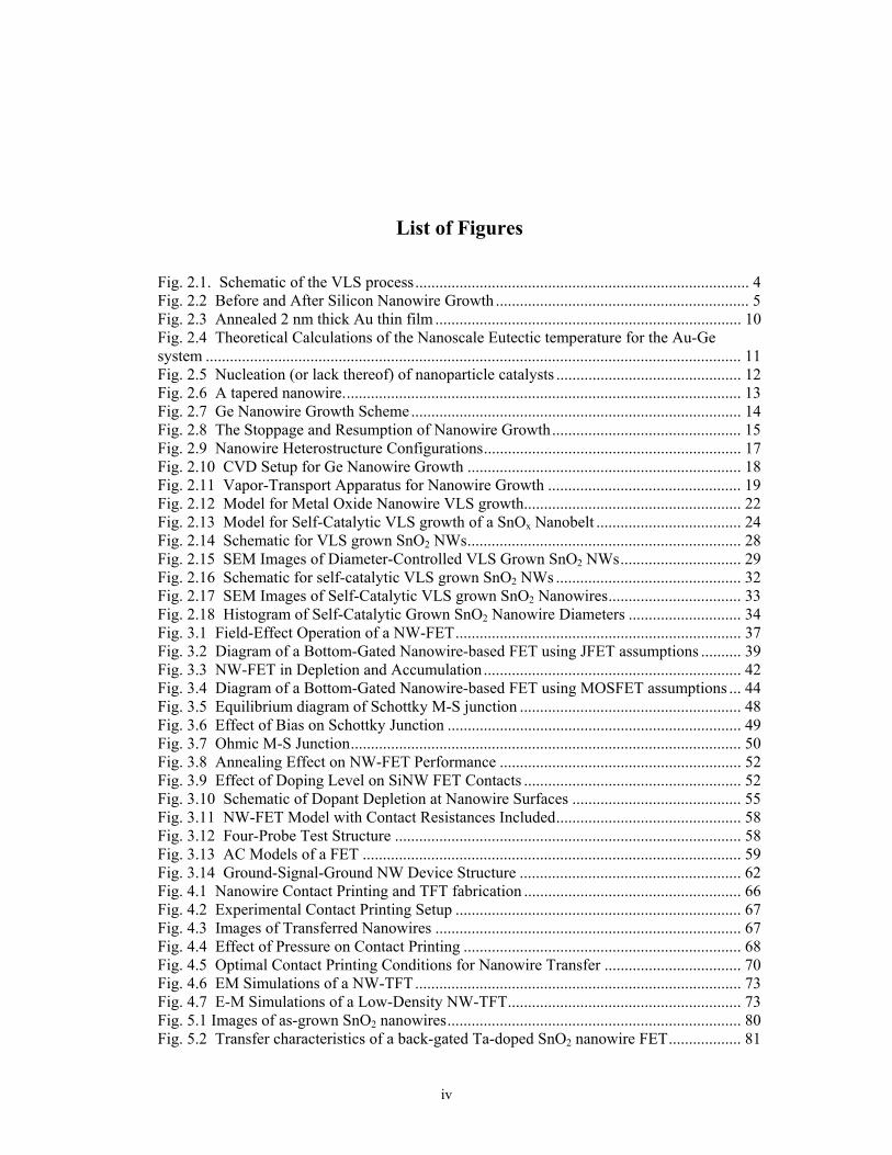
List of Figures Fig. 2.1. Schematic of the VLS process................................................................................... 4 Fig. 2.2 Before and After Silicon Nanowire Growth ............................................................... 5 Fig. 2.3 Annealed 2 nm thick Au thin film ............................................................................ 10 Fig. 2.4 Theoretical Calculations of the Nanoscale Eutectic temperature for the Au-Ge system ..................................................................................................................................... 11 Fig. 2.5 Nucleation (or lack thereof) of nanoparticle catalysts .............................................. 12 Fig. 2.6 A tapered nanowire................................................................................................... 13 Fig. 2.7 Ge Nanowire Growth Scheme.................................................................................. 14 Fig. 2.8 The Stoppage and Resumption of Nanowire Growth............................................... 15 Fig. 2.9 Nanowire Heterostructure Configurations................................................................ 17 Fig. 2.10 CVD Setup for Ge Nanowire Growth .................................................................... 18 Fig. 2.11 Vapor-Transport Apparatus for Nanowire Growth ................................................ 19 Fig. 2.12 Model for Metal Oxide Nanowire VLS growth...................................................... 22 Fig. 2.13 Model for Self-Catalytic VLS growth of a SnOx Nanobelt .................................... 24 Fig. 2.14 Schematic for VLS grown SnO2 NWs.................................................................... 28 Fig. 2.15 SEM Images of Diameter-Controlled VLS Grown SnO2 NWs.............................. 29 Fig. 2.16 Schematic for self-catalytic VLS grown SnO2 NWs .............................................. 32 Fig. 2.17 SEM Images of Self-Catalytic VLS grown SnO2 Nanowires................................. 33 Fig. 2.18 Histogram of Self-Catalytic Grown SnO2 Nanowire Diameters ............................ 34 Fig. 3.1 Field-Effect Operation of a NW-FET....................................................................... 37 Fig. 3.2 Diagram of a Bottom-Gated Nanowire-based FET using JFET assumptions .......... 39 Fig. 3.3 NW-FET in Depletion and Accumulation ................................................................ 42 Fig. 3.4 Diagram of a Bottom-Gated Nanowire-based FET using MOSFET assumptions ... 44 Fig. 3.5 Equilibrium diagram of Schottky M-S junction ....................................................... 48 Fig. 3.6 Effect of Bias on Schottky Junction ......................................................................... 49 Fig. 3.7 Ohmic M-S Junction................................................................................................. 50 Fig. 3.8 Annealing Effect on NW-FET Performance ............................................................ 52 Fig. 3.9 Effect of Doping Level on SiNW FET Contacts ...................................................... 52 Fig. 3.10 Schematic of Dopant Depletion at Nanowire Surfaces .......................................... 55 Fig. 3.11 NW-FET Model with Contact Resistances Included.............................................. 58 Fig. 3.12 Four-Probe Test Structure ...................................................................................... 58 Fig. 3.13 AC Models of a FET .............................................................................................. 59 Fig. 3.14 Ground-Signal-Ground NW Device Structure ....................................................... 62 Fig. 4.1 Nanowire Contact Printing and TFT fabrication ...................................................... 66 Fig. 4.2 Experimental Contact Printing Setup ....................................................................... 67 Fig. 4.3 Images of Transferred Nanowires ............................................................................ 67 Fig. 4.4 Effect of Pressure on Contact Printing ..................................................................... 68 Fig. 4.5 Optimal Contact Printing Conditions for Nanowire Transfer .................................. 70 Fig. 4.6 EM Simulations of a NW-TFT................................................................................. 73 Fig. 4.7 E-M Simulations of a Low-Density NW-TFT.......................................................... 73 Fig. 5.1 Images of as-grown SnO2 nanowires......................................................................... 80 Fig. 5.2 Transfer characteristics of a back-gated Ta-doped SnO2 nanowire FET.................. 81
iv

Fig. 5.3 Extraction of Average Mobility................................................................................ 82 Fig. 5.4 Electrical characterization of a typical undoped SnO2 nanowire device in air. ........ 82 Fig. 5.5 Back-gated Ta-doped SnO2 nanowire FET fabricated on glass with ITO contacts.. 85 Fig. 5.6 Degenerately Doped TAO NWs............................................................................... 88 Fig. 5.7 Electrical Characteristics Degenerately Doped TAO NWs...................................... 88 Fig. 5.8 ITO Nanowires ......................................................................................................... 90 Fig. 6.1 Overview of NW-TFT .............................................................................................. 92 Fig. 6.2 Transmittance Measurements of the NW-TFTs ....................................................... 93 Fig. 6.3 DC Characteristics of a Transparent SnO2 NW-TFT ............................................... 95 Fig. 6.4 RF characterization of transparent NW-TFTs. ......................................................... 96 Fig. 6.5 RF Characterization, cont. ........................................................................................ 97 Fig. 6.6 SnO2 NW-TFT With Optimized PECVD Dielectrics............................................. 102 Fig. 6.7 N-type SnO2 NW-TFT Inverter .............................................................................. 103 Fig. 6.8 Spice Simulation of SnO2 NW-TFT ....................................................................... 107 Fig. 6.9 Spice Simulation of SnO2 NW-TFT Inverter ......................................................... 108 Fig. 7.1 Ge/Si Core-shell NW-TFT ..................................................................................... 112 Fig. 7.2 Transparent Contacts to Ge/Si NWs....................................................................... 114 Fig. 7.3 Ge NW-TFT testing................................................................................................ 116 Fig. A.1 TEM image of ZnO film stack............................................................................... 126 Fig. A.2 TLM measurements of ZnO film........................................................................... 127 Fig. A.3 Long-Channel ZnO TFT........................................................................................ 129 Fig. A.4 Short Channel ZnO TFT........................................................................................ 131 Fig. A.5 Top-gated ZnO TFT .............................................................................................. 132
v

List of Tables Table 4.1 Optimal Contact Printing Conditions................................................................... 69 Table 6.1 SPICE Model for NMOS Component ............................................................... 107 Table A.1 ZnO TLM Measurement Results ...................................................................... 128
vi

Glossary
µ mobility (cm2/V•s)
Cgd capacitance between gate and drain (F/cm)
Cgs the coupling capacitance between the gate electrode and the FET or TFT channel (F/cm2)
Cgs capacitance between gate and source (F/cm)
Ci the coupling capacitance between the gate electrode and the NW-FET channel (F/cm)
Ec, Ev conduction band, valence band edge (eV)
EF equilibrium Fermi level (eV)
Ei intrinsic level (eV)
fmax power gain cutoff frequency (Hz)
fT unity current gain cutoff frequency (Hz)
gm transconductance (S)
I current (A)
IDS channel current in a FET, from drain to source (A)
J current density (A/cm2)
L length of a transistor, distance between the source and drain contacts (cm)
MSG Maximum Stable Gain
Qch(x) amount (magnitude) of charge at a certain location, x, of the NW channel (C)
S subthreshold slope (mV/decade)
Va applied voltage (V)
Vbi built-in contact potential, ϕm – ϕs (V)
Vch(x) is the voltage value that the channel possesses at a location (V)
VDS drain voltage with respect to source (V)
VGS gate voltage with respect to source (V)
vii

VT FET threshold voltage (V)
ε, εr, ε0 permittivity, relative dielectric constant, permittivity of free space; ε = εr • ε0 (F/cm)
ϕ work function potential (V)
ϕB Metal-semiconductor barrier height (V)
ϕm metal work function (V)
ϕs semiconductor work function (V)
ϕS surface potential (V)
χ electron affinity (V)
viii

Abstract
Metal oxide and semiconductor nanowires have shown great potential as the basis
for electronic devices which are compatible with a wide range of device substrates,
including transparent or flexible substrates. The development of such nanowire-
based devices, however, currently presents several outstanding challenges. Besides
the various issues related to the growth of nanowires, the commercial applications of
these materials depend critically on the development of scalable methods for
achieving nanowire assembly and integration. In order to address such
manufacturability issues, a thin-film transistor (TFT) based upon metal oxide
nanowires is characterized in order to show that it is possible to fabricate nanowire
devices which offer both high-performance levels and compatibility with transparent
and flexible device substrates.
Instead of directly depositing semiconductor materials on glass or plastic as with
typical TFT designs, in this work the low-temperature requirements of glass and
plastic substrates are satisfied by employing a contact printing process to transfer
synthesized nanowires from their growth substrate directly onto the device substrate.
This method was shown to effectively achieve the isolation of the high-temperature
processes required by single-crystalline material growth from the low-temperature
conditions mandated by the device substrate.
Semiconductor nanowires, such as metal oxide SnO2 or Ge-based nanowires, were
ix

x
employed as the TFT channel material. Optimization of the growth process of these
nanowires is discussed. For instance, the diameter controlled growth of 30 nm
diameter SnO2 nanowires is examined. Electrical characterization results of such
SnO2 nanowires showed that they possess field-effect mobilities that averaged 156
cm2/V•s. Moreover, by properly controlling the amount of extrinsic dopants during
the nanowire growth, the conductivity of the nanowires may be adjusted from
semiconducting to metallic.
Although the DC performance of nanowire-based transistors has been extensively
examined; in circuit applications, the high frequency characteristics of the nanowire-
based transistors are more relevant. In order to demonstrate their suitability for high
frequency circuit applications, direct RF measurements are carried out on nanowire-
based TFTs fabricated on glass. Operational speeds in excess of 300 MHz were
reached. Additionally, the suitability of these TFTs in logic circuits is demonstrated
with the fabrication and successful operation of a two-transistor inverter.
Chapter 1
1 Introduction
The nascent field of nanowire (NW) research has made a great deal of progress in
broadening the field of knowledge related to nanowire growth mechanisms and their
associated electrical properties. So far, the main focus of this research has been on single
nanowire device structures [1]. Although these simple structures are useful for probing
the intrinsic physical properties of NWs, they are not applicable to commercial or real-
world applications. A practical NW-based electronic device must be able to be fabricated
in sizable quantities and in an affordable fashion while maintaining a good uniformity in
performance among different devices. The purpose of this thesis work is to demonstrate
nanowire growth and fabrication methods which could help make NW-based electronic
devices a practical reality.
The bright prospects related to NW-based electronics can be attributed to the unique
physical properties of nanowires. As a result of their growth mechanism, nanowires may
be synthesized in an independent step and later be transferred (post-growth) to device
substrates of interests. Moreover, the nanowires to be discussed also possess a single-
crystalline structure which allows for higher speed electronic carrier transport as
compared to poly-crystalline or amorphous materials.
The device structure to be presented that can take advantage of these properties in a
practical manner is the nanowire-based thin-film transistor (NW-TFT). The main
1

novelty of a NW-TFT as compared to other electronic devices is that the switching
element, i.e. semiconductor channel material, is made up of an array of a large number of
aligned nanowires. Such NW arrays may be transferred onto a wide variety of substrates,
like glass, in a controlled fashion by a contact printing method. Following the nanowire
transfer to the substrate of interest, device fabrication can be carried out using established
semiconductor processing methods. The fabrication of NW-TFTs on transparent
substrates like glass opens up the possibility of achieving transparent electronic devices.
The operation of a transparent NW-TFT and a two-transistor inverter will be examined.
For practical circuit applications, both p- and n-type transistors are required. To this
end, p- and n-type NW-TFTs were fabricated separately in this work and both their DC
and RF electrical properties will be detailed. The semiconductor SnO2 was utilized as the
n-type material, while Ge-based nanowires were explored as the p-type material. A
future goal will be to fabricate both structures on the same chip with the aim of creating
low-power, complementary logic circuits.
Lastly, the electrical characterization of a single-crystalline ZnO TFT on a Si substrate
will be examined in Appendix A. Although not a nanowire-based device, the ZnO TFT
shares many structural similarities with NW-TFTs, and serves as a useful performance
comparison. Thanks to its epitaxial deposition on Si, the structure of the examined ZnO
TFT could one day be useful in integrating ZnO devices alongside Si-based devices.
2

Chapter 2
2 Nanowire Growth
2.1 Overview
The bottom-up growth of nanowires may be achieved by a variety of methods [1-3],
such as solution-phase or template-directed deposition. This work will, however,
exclusively focus on the vapor-based growth of nanowires and specifically via the vapor-
liquid-solid (VLS) process. The VLS process was first demonstrated in the 1960s by
Wagner with the growth of silicon whiskers (wire-like structures 100s of nm to microns
in diameter) [4]. The name for the VLS process was coined to describe the step-by-step
phase changes of the reactant molecules as they proceed through the entire crystal growth
process. It is important to note that the VLS growth process possesses many different
characteristics as compared to plasma or thermal chemical vapor deposition (CVD)
processes. Whereas traditional CVD relies upon the thermal (or plasma) activated
decomposition of gaseous reactants, the VLS process utilizes a metal catalyst to facilitate
the deposition of the gaseous reactants. Typically, VLS depositions may occur at lower
temperatures and produce products with a greater crystalline quality than low-
temperature thermal or plasma-CVD processes.
The role of the metal catalyst will first be examined. Two requirements for this metal
catalyst are: a) that the metal be able to alloy with the desired reactant element, and b)
that the metal catalyst forms an eutectic alloy with the reactant element. An eutectic
3

alloy is defined as an alloy such that at some alloy composition ratio, the melting point of
the alloy is less than both of the individual pure elements [5]. Not necessarily all alloys
are eutectic.
As a generality in VLS growth, the diameter of the metal catalyst particle roughly
determines the diameter of the grown nanowire. For example, if large catalyst particles
are used (i.e. micron sized metal particles), then large, micron-sized whisker structures
will be obtained from VLS growth, as was first established by Wagner in the 1960s [4].
Metal nanoparticles may be deposited directly onto a growth substrate. The diameter and
density of the deposited nanoparticles directly influences these same properties of the
grown nanowire forests. If growth in only certain areas is desired, the nanoparticles may
be patterned via means such as photolithography [6].
Fig. 2.1. Schematic of the VLS process a) Diagram of the VLS Process. The steps to this process are: alloy droplet formation (I), nanowire nucleation (II), nanowire axial growth (III). Adapted with permission from [7]. Copyright 2001 American Chemical Society. b) Binary Phase Diagram of the Au/Ge alloy. The green line is the Au liquidus line, and the blue line is the Ge liquidus line. The eutectic point of the system is marked by an arrow. The solidus line (horizontal) is in black at the eutectic temperature. Adapted from [8]. Reprinted with permission from AAAS.
The VLS process will now be examined sequentially according to Fig. 2.1 which
diagrams the growth of a Ge nanowire using an Au catalyst [7-8]. The VLS growth of a
nanowire can be summarized into three steps: (I) liquid alloy droplet formation, (II)
4

nanowire nucleation, and (III) nanowire elongation (i.e. growth). This process is
displayed schematically in Fig. 2.1a. In addition, the process may also be plotted on a
phase diagram for the alloy system (Fig. 2.1b). This phase diagram is specifically known
as a binary eutectic phase diagram, where the independent variables are the alloy
compositional percentage and the temperature; the experimental data (data of interest) is
the phase of matter of the materials.
a) b)
Fig. 2.2 Before and After Silicon Nanowire Growth a) AFM image of 10 nm Au nanoparticles on a growth substrate. b) SEM image of Si nanowires grown after CVD VLS process. Inset, the solidified alloy droplet can be seen at the end of the nanowire when imaged post-growth. The sides of both images are 4 μm. Reprinted with permission from [9] . Copyright 2001, American Institute of Physics.
To go into more detail about the phase diagram, one can notice from Fig. 2.1b that the
Au/Ge alloy is eutectic, where the melting point of Au and Ge is 1064 °C and 938 °C,
respectively. The eutectic point for an eutectic alloy system is defined as the temperature
and compositional gradient at which the alloy has its lowest melting point. The eutectic
point is important since the liquid and solid phases of the material system are all allowed
to exist simultaneously at these conditions. The eutectic point for the bulk Ge/Au system
is 28% Ge atomic percentage, 361 °C. The green and blue lines on the plot are the Au
and Ge, respectively, liquidus lines. They represent the boundary above which these
5

materials are liquid, and below which are solid. The solidus line (black, horizontal) line
occurs at the eutectic temperature (361 °C) and represents the temperature below which
the alloy must be solid.
Fig. 2.1 illustrates the VLS growth process of a Ge nanowire at ~800 deg C as
examined in ref. [7]. This temperture was chosen by the experimenters due to constraints
in their experimental setup. Ge nanowire VLS growth may occur at temperatures
between the melting point of Ge (938 °C) and the eutectic temperature of the Ge/Au
alloy. It is important to note that Ge nanowire VLS growth has been observed at
temperatures down to ~270 °C [10] due to reasons that will be discussed later.
In step I, liquid Ge/Au alloy droplet formation, the Au catalyst sites are heated up in
the presence of a vapor source of Ge (typically GeH4). Liquid droplets will start to form
above the eutectic temperature for the nanoscale alloy system. Note that without the
presence of gaseous Ge molecules, the Au catalyst sites will not liquefy at the eutectic
temperature. Direct TEM observation of Au nanoparticles heated up to 900 °C in a
vacuum (without any gaseous Ge source) revealed that the Au did not liquefy [7]. The
diffusion of Ge atoms into the Au cluster sites is required for the Ge/Au alloy droplet
formation. When CVD reactants are used (i.e. GeH4), the temperature is a crucial factor
for the dissociation of the reactant precursor molecule and the subsequent absorption of
the Ge atoms. GeH4 readily dissociates at low temperatures (i.e. ~270 °C) at metal
catalyst sites while other CVD precursors (i.e. SiCl4) require high temperatures (i.e. 800
°C or above) for reactant dissociation when carrying out Si nanowire VLS growth [6].
During droplet formation, the metal nanoparticle site serves as a catalyst for the
decomposition of the reactant molecules by lowering the thermodynamic energy barrier
6

required for reactant dissociation and subsequent crystal (nanowire) formation. Due to
this energy barrier lowering, materials may preferentially deposit at these catalyst sites
and cause nanowire growth while leaving the rest of the growth substrate free of any
deposition, as evidenced in Fig. 2.2.
It was originally suggested by Wagner [4] that a reason for this catalytic activity of the
metal catalyst particle was due to the high sticking coefficient that a liquid droplet
presents to a gaseous reactant (like SiH4) as compared to the solid, bare growth substrate.
A sticking coefficient is defined as the probability that an impingent molecule attaches to
a certain surface upon collision. It is true that silanes have a larger sticking coefficient on
liquids catalysts as compared to typical growth substrates, however this phenomenon
cannot explain all VLS growth processes, especially when the growth material is not a
reactant molecule, but rather evaporated from a solid source [11]. Although the exact
source for the catalytic activity of the metal nanoparticle is still under debate, under
typical VLS growth conditions the metal nanoparticle’s catalytic properties allow for it to
act as a sink for gaseous material sources and for the exclusive incorporation of these
materials for nanowire growth as opposed to substrate or sidewall deposition.
As the VLS process proceeds, the adsorption of the growth material (Ge) and its
incorporation into the liquid alloy droplet will cause the alloy to increase the saturation
ratio of Ge in the originally 100% Au nanoparticle. It is illustrative to examine an
isothermal line (at 800 °C) for this specific saturation of Ge into the Au nanoparticle as
shown in Fig. 2.1b. It is thermodynamically allowed for the Ge incorporation to continue
into the droplet along the horizontal isothermal line until one reaches the Ge atomic
concentration rate which intersects the Ge liquidus line (blue). Beyond this concentration
7

of Ge, any further increase in Ge percentage in the liquid alloy is defined as
supersaturation. Although the condition of supersaturation is not thermodynamically
favored, it may exist in a state of unstable equilibrium due to the fact that the way to
resolve this unfavored state, which is crystal nucleation, requires a certain energy input to
initiate [8]. As time goes on and Ge continues to incorporate into the droplet, a critical
supersaturation ratio is reached where the unstable equilibrium can no longer be
maintained, and nucleation of the nanowire will occur (step II). Nucleation is defined
here as the formation of a crystal phase.
Subsequent to the nanowire nucleation, further incorporation of the Ge species will
cause nanowire elongation (i.e. axial growth, step III). It is explained that this additional
supersaturation of Ge species causes additional Ge crystal precipitation (i.e. nanowire
growth) as opposed to additional nucleation events due to the fact that less energy is
needed for crystal growth as compared to additional nucleation events in the droplet.
Nanowire growth continues as long as a sufficient partial pressure of gaseous Ge material
is present or the temperature is sufficient. As soon as these conditions cease, the alloy
droplet expels the supersaturated portion of the Ge via the nanowire growth mechanism
and the liquid alloy droplet will be left at an eutectic alloy concentration.
2.2 Important Aspects related to VLS Nanowire Growth
2.2.1 Nanoparticle Catalysts
The choice of metal catalyst for VLS growth plays a critical role. As previously
mentioned, the metal catalyst must be able to form an eutectic liquid alloy with the
certain nanowire growth species. Moreover, the solid solubility of the catalyst in the final
single-crystalline material must be low so as to minimize crystal defects. For instance,
8

Au is commonly used to catalyze Si nanowire VLS growth, and the maximum solid
solubility of Au in Si is just ~2x10⁻⁴ at.% at 1280 °C [12], making it an appropriate
choice.
Another important consideration is whether the metal catalyst can alternatively
perform nanowire growth via the vapor-solid-solid (VSS) process. VSS growth proceeds
similarly to the VLS process, a catalytic metal nanoparticle acts as a growth site for a
nanowire single-crystal. Unlike the VLS process, VSS growth proceeds with the metal-
rich catalyst particle remaining in a solid state throughout the entire growth process [13].
One notable feature of the VSS process is that it can take place far below the eutectic
temperature of the catalyst and crystal material alloy. For instance, Si nanowire growth
with Cu catalysts has been demonstrated via the VSS mechanism at ~400 °C while the
eutectic temperature of the system is ~800 °C [13]. Moreover, the VSS nanowire growth
typically proceeds 10-100x slower as compared to VLS growth under comparable
conditions [14]. Both VLS and VSS growth have been observed occurring at the same
time in a single growth chamber [8]; therefore in order to maintain good control over
nanowire growth it necessary to properly control and choose the appropriate growth
mechanism. Au is often chosen as the alloy for VLS growth due to the fact that it
possesses a low eutectic temperature in most alloys that it forms, suppressing the
likelihood of VSS growth.
The density and morphology of the metal nanoparticles are a critical determinate of
nanowire growth. Since VLS grown nanowires roughly take on the diameter of the metal
catalyst nanoparticle, the presence of a wide distribution of nanoparticle sizes will
produce nanowires possessing the same large size distribution [15]. To mitigate these
9

effects, the most popular method of placing metal catalysts on a substrate is the
dispersion of metal liquid colloids (i.e. colloidal Au). These liquid colloids consist of
metal nanoparticles stabilized in a liquid suspension [9]. As seen in Fig. 2.2, the
nanowires produced using such nanoparticles are of a very uniform diameter. Clumping
of the deposited nanoparticles on the substrate must be avoided, however, in order to
ensure that the nanoparticle catalysts do not combine together under the high
temperatures of VLS growth. Since the nanoparticles become liquid alloys under VLS
growth, in such conditions they may readily combine with other physically adjacent
nanoparticles. The appropriate choice of nanoparticle density is known to reduce the
chance of this occurring.
Fig. 2.3 Annealed 2 nm thick Au thin film Reprinted with permission from [11]. Copyright 2001, American Institute of Physics.
Another widely used method for creating metal nanoparticles is through the annealing
of metal thin films. These metal thin films are typically deposited in thicknesses of ~1
nm to ~100 nm. The metal thin film may be annealed at appropriate temperatures (i.e.
~500 °C for Au thin films [11], Fig. 2.3) to cause the film to ball up into separate islands
of metal with a non-uniform size distribution [16]. It is clearly noted in Fig. 2.3, that
there are nanoparticles of a large diameter (greater than 100 nm) on the substrate. After
10

carrying out Ge nanowire growth, the authors measured the diameters of the synthesized
nanowires in the range of 20-180 nm.
2.2.2 Nanoscale Eutectic Temperature
Fig. 2.4 Theoretical Calculations of the Nanoscale Eutectic temperature for the Au-Ge system Adapted with permission from [17]. Copyright 2007 American Chemical Society.
For nanoscale systems (i.e. metal nanoparticles or thin films), it has been widely
noted that an alloy’s eutectic temperature is typically suppressed [18] from the well-
known bulk values. This effect contributes to the reduction of the minimal temperature
necessary for nanowire VLS growth. For instance, as displayed in Fig. 2.4, the eutectic
temperature of 10 nm diameter Au nanoparticles in the presence of Ge species
experiences a much lower eutectic temperature (~300 °C) as compared to the bulk system
(~360 °C). In addition to the eutectic temperature lowering due to size-related effects,
the supersaturation of the alloy droplets with high Ge concentration during VLS growth
is also hypothesized to keep the Ge/Au alloy in the liquid state even further below the
bulk eutectic temperature [8, 17], allowing for Ge nanowire VLS growth at temperatures
as low as ~260 °C.
11

2.2.3 Nucleation of Nanoparticles
Although ideally in VLS growth there should be a 100% nucleation rate of each
catalyst nanoparticle to initiate the growth of an individual nanowire, this does not always
happen under practical conditions. As displayed in Fig. 2.5, it is possible for a single
metal catalyst nanoparticle to either: (a) not nucleate nanowire growth at all, (b) nucleate
a single nanowire growth, or (c) nucleate multiple nanowire growth fronts. The most
important factors that were found to determine these effects were the growth temperature
and the partial pressure of the reactants [10]. Under higher growth temperatures and
higher partial pressures of the growth reactants, more nucleation events occurred.
Fig. 2.5 Nucleation (or lack thereof) of nanoparticle catalysts SEM images of Ge nanowire growth under different conditions (only temperature is varied). a) less than 100% nucleation of Ge nanowires, b) one-to-one nucleation of Ge nanowires from Au nanoparticle catalysts, c) multiple nanowire growths from Au catalyst sites. Scale bar is 5 µm for a and b and 1 µm for c. Reproduced with permission from [10, 19]. Copyright Wiley-VCH Verlag GmbH & Co. KGaA.
2.2.4 Nanowire Sidewall Deposition
In the idealized VLS nanowire growth mechanism, deposition of material on the
grown nanowire sidewalls is assumed not to occur. However, under certain conditions
this may in fact take place, leading to the growth of tapered nanowires (Fig. 2.6).
Tapered nanowires feature a wide base and narrow top (the end where axial growth
ceases). This morphology is due to the fact that sidewall deposition is typically
homogenous and occurs at a uniform rate on a nanowire; thus, the oldest grown segments
of the nanowire experience the most deposition and the newly grown sections of a
12

nanowire will experience the least amount of total sidewall deposition.
Fig. 2.6 A tapered nanowire. TEM image of the growth of a tapered Ge nanowire. From left to right, is an image of the same Ge nanowire as the growth proceeds. Adapted from [8]. Reprinted with permission from AAAS.
Various strategies for reducing or eliminating sidewall deposition have been
demonstrated. Two parameters known to play a large role in uncatalyzed deposition are
growth temperature and the partial pressures of reactants. Increasing either parameter
will increase the amount of thermal decomposition of material species on grown
nanowires and the substrate itself [10]. To carry out proper nanowire growth, these two
parameters must be properly adjusted to address the two important needs of: (1) high
yield nanowire nucleation, and (2) the prevention of sidewall deposition.
Ge nanowire growth provides a good example of the rational choice of the growth
temperature in order to address these two simultaneous needs. It has been established
that Ge nanowires grown from GeH4 are particularly susceptible to uncatalyzed sidewall
deposition if grown near the bulk eutectic temperatures on Ge and Au (~360 °C) [17]. A
successful method to achieve both high nucleation rates and uniform nanowire diameters
is through the use of a two-step growth process as displayed in Fig. 2.7. A higher
temperature is used initially in the VLS growth process in order to cause the nucleation of
a large percentage of the alloy nanopaticle droplets. Then, once high yield nucleation is
13

achieved, the temperature is ramped down to a lower level to prevent sidewall deposition
while simultaneously providing sufficient nanowire axial elongation growth rates.
Another strategy involves the use of an appropriate carrier gas to functionalize the
grown nanowire surfaces with the correct functionalization group which prevents
sidewall deposition. This was demonstrated with the use of H2 as a carrier gas in order to
H- terminate silicon nanowires during VLS growth [20]. Additionally, the use of local
substrate heaters (as opposed to hot-wall chambers) has been shown to reduce the amount
of unwanted thermal decomposition of CVD reactants and thus reduce nanowire sidewall
deposition [20].
Fig. 2.7 Ge Nanowire Growth Scheme Two temperature VLS growth process where first high yield nanowire nucleation is achieved at a high temperature, followed by axial elongation and no sidewall deposition at a lower temperature. Reprinted with permission from [21]. Copyright 2004, American Institute of Physics.
2.2.5 Nanowire Growth Rates
Another essential parameter for nanowire growth is the rate of axial elongation of the
nanowire. Depending on deposition conditions, this rate can be drastically altered. For
instance, the CVD reactant Si2H6 was found to produce nanowires at growth rates over
100x as great as compared to SiH4 [22]. It was reasoned that Si2H6 more readily
decomposes as compared to SiH4. Besides the choice of reactant species, other
14

parameters which play a critical role are the temperature and partial pressure of the
reactance species [23]. Increasing either of these parameters will also increase the
nanowire growth rate.
Specifically, it has been shown that the amount of supersaturation of the crystal
growth material in the liquid alloy nanoparticle is directly influenced by the partial
pressure of the gaseous reactants. This amount of supersaturation is what directly effects
nanowire growth rates. Thus, it has been observed that typically a higher partial pressure
of the reactants leads to higher growth rates [24]. This can be most dramatically seen in
Fig. 2.8, where nanowire growth can be repeatedly stopped and restarted by simply
purging and reflowing gaseous reactants into the growth chamber. Completely purging
the chamber lowers the amount of supersaturation of the alloy droplet causing growth to
cease. When reactants are again flowed in, high supersaturation levels are restored in the
droplet, and a new nucleation event occurs, followed by the continuation of nanowire
growth. The evidence of these additional nucleation steps can be evidently seen in the
kinks (abrupt ends) of the nanowire.
Fig. 2.8 The Stoppage and Resumption of Nanowire Growth a) Schematic of a cyclical method to stop and restart nanowire growth. During nanowire growth (1), reactants may be purged from the growth chamber, ceasing growth (2). Growth may be restarted by flowing in reactants again (3). b) SEM image of a kinked Si nanowire. Scale bar is 1 µm. Reprinted by permission from Macmillan Publishers Ltd: Nature [24] copyright 2009.
15

2.2.6 Nanowire Heterostructures
Another benefit that the bottom-up growth of nanowires provides is that different
materials may be incorporated into a single nanowire in a heterogeneous configuration
during growth. A schematic of the possible configurations of the heterogeneous
nanowire material structure is shown in Fig. 2.9. The base case (starting point) to
heterogeneous nanowire growth is the VLS growth of a single material nanowire (Fig.
2.9a). The VLS growth process has already been extensively covered earlier in this
chapter. By modifying the reactant gases during VLS growth, axial or radial material
nanowire heterostructures may be obtained. An axial heterostructure (Fig. 2.9b), where
the material varies along the long axis of the nanowire, can be achieved by varying
reactants during the axial elongation phase of VLS growth.
Radial heterostructures (Fig. 2.9c), where the material composition varies
symmetrically along the radial cross-section of a nanowire, are synthesized by
performing sidewall (i.e. homogeneous) deposition of a new material after axial
elongation of the nanowire is ceased. A two-material radial heterostructure, as depicted
in Fig. 2.9c, is typically termed a core-shell nanowire, where the core comprises of the
starting nanowire material, and the shell is made up of the later, homogeneously
deposited exterior material. The limit to the amount of shells capable of being deposited
is in theory unlimited, but the practical limit is determined by the specific material system
being deposited.
16

Fig. 2.9 Nanowire Heterostructure Configurations Description given in text. Arrow denotes preferential site for reactant adsorption. Reprinted with permission from [25]. Copyright 2003, Materials Research Society.
2.3 Nanowire Growth Setups
2.3.1 CVD Nanowire Growth
One of the most common setups used to carry out the VLS growth of nanowires is in a
low-pressure CVD, i.e. LPCVD, apparatus (Fig. 2.10). Typically, the setup comprises of
a two-ended quartz tube placed in a ceramic-encased resistive element furnace. One end
of the tube (the inlet side) is hooked up to mass flow controllers (MFCs) which regulate
the input flow of compressed process gases. Besides the main process gas (i.e. SiH4 or
GeH4), there may be also be dopant gases or dilutant gases (i.e. H2 or Ar) fed into the
growth chamber. The other end of the tube (outlet side) is hooked up to a vacuum pump
via an adjustable vacuum throttle valve. The nanowire growth substrates are placed in
the center of the tube furnace where temperature uniformity is the highest.
The nanowire growth is typically run at low to medium vacuum (~1 to 760 torr) and
this is controlled by properly adjusting the inlet flow of the gases as well as the strength
of the vacuum pump via its throttle valve connection to the outlet of the tube. Similar to
conventional LPCVD systems, the major reason for low-pressure depositions is to
increase uniformity across the deposition substrates [26]. Additionally it is important to
17

be able to adjust the process pressures for VLS nanowire growth, since these parameters
directly affect all aspects of nanowire growth (as detailed earlier).
Fig. 2.10 CVD Setup for Ge Nanowire Growth Reprinted by permission from Macmillan Publishers Ltd: Nature Protocols [15] copyright 2004.
2.3.2 Vapor-Transport Metal Oxide Nanowire Growth
An alternative method for nanowire growth via the VLS method relies upon the vapor
transport of evaporated source materials from a solid source (typically in powder form).
This method is schematically similar to the CVD growth method outlined earlier, with the
one difference being that the source materials are supplied via thermal evaporation rather
than compressed gas sources. A typical setup for this process is depicted in Fig. 2.11. As
before with CVD systems, the setup comprises of a two-ended quartz tube placed in a
ceramic-encased resistive element furnace. One end of the tube (the inlet side) is hooked
up to mass flow controllers (MFCs) which regulate the input flow the compressed
carrier/process gases. The other end of the tube (outlet/exhaust side) is hooked up either
to an exhaust or a vacuum pump depending on whether atmospheric pressure or vacuum
is desired. Inside the quartz tube is first placed the source material and then downstream
18

is placed the growth substrate.
Regardless of the process pressure of the tube (either atmospheric or vacuum), a
carrier gas is supplied at the inlet end of the tube via a MFC in order to direct the
transport of the evaporated source species to the downstream growth substrate. This
carrier gas is typically either Ar or N2; the carrier gas species and flow rate are important
parameters for nanowire growth [27].
Near the middle of the tube lies the source material. During process, this area of the
furnace is heated up to a high temperature so as to create a partial pressure of the species
by thermal evaporation. This partial pressure is determined by the evaporation rate and
vapor pressure (for a certain temperature) of the source material. Downstream of the
source material is placed the growth substrate. The growth substrate is typically heated
either to the same temperature or a lower one as compared to the source material
(depending on process requirements). Additionally, the distance between the source
material and growth substrate is an important parameter which affects the amount of
material species that reach the growth substrate.
Fig. 2.11 Vapor-Transport Apparatus for Nanowire Growth Reprinted from [2] with permission from Elsevier.
19

The previously described vapor transport growth using evaporated source materials
method can grow a wide variety of nanowires, including even Si or Ge [11] nanowires,
however its use in the growth of metal oxide nanowires will be explored in detail. Metal
oxide semiconductor nanowires; such as SnO2, ZnO, or In2O3; are a class of materials
that readily lend themselves to be grown by the vapor transport growth method. In order
to synthesize oxide nanowires with this method, two options are available: either the
semiconductor oxide material may be evaporated directly (i.e. SnO2, ZnO, or In2O3
powder), or a pure metal powder (i.e. Sn, Zn, or In) may be evaporated in the presence of
O2 in the growth tube. The gaseous O2 may be supplied either via a MFC after pumping
out residual atmospheric O2 from the process tube; or instead, trace amounts of
atmospheric O2 that either leak into the tube or which are residual quantities may be
utilized. This amount of O2 is a critical parameter of nanowire growth, it not only
influences the volatility of the source material (due to competitive oxidation of the
metallic atoms) but also influences the yield, morphology, and growth rate of the
nanowires.
2.4 Metal Oxide Nanowire Vapor-Phase Growth
Metal oxide nanowires (i.e. SnO2, ZnO, or In2O3) may be grown using vapor-phase,
metal catalyzed methods which are widely assumed to be similar to the previously
detailed VLS method for Si and Ge nanowires. However, the exact growth mechanism of
metal oxide nanowires is still under much debate in the literature. The main uncertainty
lies in discerning the role of the metal catalyst during growth. The following four
separate theories on metal oxide nanowire growth will be presented: (1) VLS growth, (2)
VSS growth, (3) self-catalytic VLS growth, and (4) VS growth.
20

2.4.1 VLS Growth of Metal Oxide Nanowires
The theorized VLS growth process for a ZnO nanowire will now be described. ZnO is
chosen arbitrarily for this discussion, the process is applicable to any metal oxide
nanowire. It is proposed that the VLS growth proceeds from a binary alloy droplet of the
vapor phase Zn material and the chosen catalyst (i.e. Au). Upon sufficient
supersaturation of the droplet, Zn precipitates from the droplet at the liquid-solid
interface of the droplet and the ZnO nanowire. Oxygen is claimed not to be present in the
alloy droplet (experimental data is cited in [28]), and the makeup of the Zn/Au alloy
droplet is hypothesized to follow Wagner’s original VLS theory of a binary eutectic alloy
droplet. Gaseous oxygen atoms are next presumed to diffuse towards the Zn metal
interfacial region (but not through the Au-Zn droplet bulk) and then carry out the
oxidation of the Zn atoms into ZnO and thus elongate the nanowire [28-30].
It is important to note that the authors derived the above theory from experimental
ZnO nanowire growth that took place near the melting temperature of Zn (~420 °C) [29,
31]. This theory however does not properly explain (seemingly-VLS) ZnO nanowire
growth at temperatures far above Zn’s melting temperature, i.e NW growth has been
demonstrated at ~800 °C [32]. At such high temperatures, any precipitated Zn metal
would quickly reliquefy which invalidates the previous model. A less widely cited
proposal may explain such high temperature growths. It hypothesizes that oxygen
diffuses into the alloy droplet during growth, causing supersaturation of the metal oxide
inside the droplet, thus bringing about precipitation of the metal oxide and nanowire
growth [33]. Moreover, the self-catalytic nanowire growth process may also play a role
and will be covered in this chapter.
21

Fig. 2.12 Model for Metal Oxide Nanowire VLS growth a) a proposed model for the VLS growth of a ZnO nanowire. The vapor phase Zn atoms are presumed to form an alloy with the Au catalyst nanoparticle. Nanowire growth proceeds via the precipitation of Zn from the droplet which then forms ZnO by oxidation by oxygen atoms present in the chamber. Reprinted from [34] with permission from Elsevier. b) a more detailed schematic of this model. Oxidative species (i.e. CO/CO2 in this figure) oxidize the precipitating Zn atoms at the liquid-solid interface of the catalytic droplet and growing nanowire. Reprinted from [28] with permission from Elsevier.
In addition to ZnO, Au-catalyzed VLS growth has been used to grow many other
metal oxide nanowires, including SnO2 and In2O3 nanowires [35].
2.4.2 VSS Growth of Metal Oxide Nanowires
An alternative explanation for metal nanoparticle catalyzed ZnO nanowire growth
relies upon the vapor-solid-solid (VSS) growth mechanism. It is important to note that
this theory was derived from experimental measurements on ZnO nanowire growths that
were conducted at ~850 °C and does consistently explain growth at this high temperature
[36]. The basis for their theory is attributed to XRD measurements taken on a ZnO
nanowire forest after growth which reveal that no Zn was present in the Au catalyst
nanoparticle tips. This finding leads the authors to suggest that VSS growth occurred
rather than the more widely cited VLS method. The authors propose that the growth does
not proceed via a supersaturation-nucleation process, but rather that the Au nanoparticles
act as preferential adsorption sites for Zn species which then are incorporated in the
growing ZnO nanowire by surface diffusion along the Au nanoparticle.
22

2.4.3 Self-Catalytic Growth of Metal Oxide Nanowires
In the previous two methods, a separate catalyst metal (i.e. Au) was used in order to
catalyze the growth of metal oxide nanowires. An alternative approach to metal oxide
nanowire growth instead relies upon the self-catalytic NW growth properties of the metal
species of metal oxide nanowires. For instance, it has been shown that ZnO nanowires
have been selectively grown from Zn isolated metal islands without the use of any
additional metal catalyst by simple oxidation annealing [37-38]. Since in both references,
the reaction takes place above the melting point of Zn (~500 °C), it is hypothesized that
Zn liquid originating on the Zn islands act as a catalyst to ZnO nanowire growth [39].
The vapor-phase growth of ZnO nanowires has been demonstrated on completely bare
surfaces (i.e. SiO2 or alumina) by the thermal evaporation of either Zn metal in the
presence of O2 or ZnO powder [34, 40]. Moreover, a similar synthesis has also been
demonstrated with SnO2 nanowires [41-42]. The mechanism for such nanowire growth is
explained by two hypotheses: either self-catalytic VLS or vapor-solid (VS) growth. For
both methods, source materials are evaporated at high temperature (usually in a tube
furnace) into a vapor state and transported via carrier gas.
In self-catalytic VLS growth, the vapor phase species reaches the deposition substrate
while still in the high temperature zone, and proceeds to coalesce onto the growth
substrates to form liquid droplets. In particular, a requirement for self-catalytic VLS
growth is that the deposition substrate temperature be above the melting point of the
metal species to allow for liquid droplet formation. An example of this growth process
for a SnOx nanobelt is shown in Fig. 2.13. One theory proposed to explain the self-
catalytic growth process is that liquid metal droplets are formed which then catalyze
nanowire growth as a result of the supersaturation of metal oxide in the droplet [43]. An
23

alternative theory surmises that instead of metal oxide supersaturation in the droplet,
gaseous oxygen reacts at the surface of the droplet (not in the bulk of droplet) to form the
metal oxide nanowire [37]. Importantly, Au-catalyzed VLS growth and self-catalytic
VLS growth may proceed simultaneously. Branched SnO2 nanowires have been grown
from Au catalysts due to the self-catalysis of branched nanowire formation from adsorbed
Sn droplets on the nanowire surface [33].
Fig. 2.13 Model for Self-Catalytic VLS growth of a SnOx Nanobelt ) Sn droplet formation via the coagulation of vapor Sn atoms, b) nucleation of the SnOx nanobelt after the Sn droplet becomes supersaturated with SnOx, c) axial elongation of the nanobelt via precipitation of supersaturated SnOx, similar to the VLS mechanism. Adapted with permission from [43]. Copyright 2006 American Chemical Society.
2.4.4 Vapor-Solid Growth of Metal Oxide Nanowires
An alternative hypothesis to the self-catalytic formation of metal oxide nanowires is
the VS growth process, whereby metal oxide vapor directly deposits onto the growth
substrate in solid form. As a distinction to the VLS process, there is no intermediate
liquid phase present. Crystal nucleation occurs directly as vapor metal oxide species
condense (and solidify) onto a growth substrate. Nanowire growth proceeds due to the
fact the nanowire growth front presents a thermodynamically favorable place for
additional vapor phase species to solidify. Notably, the VS process is able to cohesively
explain the self-catalytic growth of metal oxide [44] and even metal [45] nanowires on
24

deposition substrates held at temperatures lower than the melting point of the metal
species. Furthermore, the VS process has also been deduced to operate at temperatures
above the metal melting point [46] due to the fact that metal oxides typically possess
melting temperatures greater than the metal element itself. A disadvantage of the VS
process is that it is difficult to control the morphology of the grown nanowires (i.e.
diameter) since no separate metal catalyst is required.
2.4.5 Experimental Results for Vapor-Transport Growth of SnO2 Nanowires
2.4.5.1 Diameter-Controlled Vapor-Liquid-Solid SnO2 NW Growth
The diameter-controlled growth of vapor-liquid-solid grown SnO2 nanowires will be
detailed in this section. Although such growth was only demonstrated in a small area (<
1 mm2) on a growth substrate which was not sufficient for device fabrication purposes,
the demonstration does illustrate that such growths are in principle feasible. As described
in section 2.4.1, nanoparticle-nucleated vapor-liquid-solid growth of nanowires is
observable only under certain proper conditions, i.e. certain gaseous precursor vapor
pressures and appropriate growth temperatures. At improper conditions, VLS nanowire
growth will not be observed, but rather other material depositions will occur such as
homogeneous material deposition which will be detailed in section 2.4.5.2.
Experimental Conditions
We were able to achieve a sufficient control over the deposition parameters and in turn
VLS SnO2 nanowire growth by utilizing the growth setup shown in Fig. 2.14. Growth
was carried out in a single-zone horizontal tube furnace with tube inner diameter of 2 1/8
inches and length of 40 inches. The temperature ramp rates were fixed at 10 °C/min. A
25

Sn powder precursor, procured from Sigma Aldrich, 99.8% pure, was used as the Sn
precursor source and was placed in the center of an alumina ceramic boat, the dimensions
of the boat and weight of the Sn powder are described in Fig. 2.14.
The nanowires were grown on a Si substrate (7x1 cm2) in which Au nanoparticles
were deposited onto. Au nanoparticles colloidal solutions were procured from Ted Pella
and diluted to a concentration of ~1010 particles/mL. Poly-l lysine functionalization of
the Si surface was utilized in order to promote Au nanoparticle adhesion. The obtained
nanoparticle deposition density was in the range of 1-5 nanoparticles / μm2. 20 nm
diameter Au nanoparticles were used for the growth process described in this section.
As shown in Fig. 2.14, the growth substrates were placed directly on top of the Sn
powder source and let to lie flat on the top of the ceramic boat. The growth substrates
were placed such that their nanoparticle-functionalized surfaces were orientated
downwards closest to the Sn powder source. By only using a small amount of Sn powder
(0.1 g) confined to a 1 cm long region in the center of the 10 cm long ceramic boat, a Sn
vapor gradient was able to be produced during the high-temperature growth conditions.
Specifically, during the growth process the Sn vapor pressure was highest in the volume
of space contained by the ceramic boat directly closest to the Sn powder precursor. This
Sn vapor pressure then monotonically decreased in the ceramic boat in a proportion that
was directly related to the distance away from the center of the boat where the Sn powder
precursor was situated.
The growth process proceeded as follows. The ceramic boat with Sn powder and with
the Si growth substrate situated on top of the boat was placed in the center of the tube
furnace. An Ar gas flow, acting as the carrier gas, of 0.7 SCFH was made to flow
26

through the tube using metered flows and at atmospheric pressure. The tube was allowed
to heat up to 900 °C and was held there for 25 min. After this time elapsed, the furnace
was opened and the ceramic boat was pulled out from the center of the furnace using a
stainless steel rod while the furnace was still at the process temperature and let to cool at
the end of the ceramic tube.
Results
Following growth, SEM imaging of the growth substrate at an area situated 1.5 cm
downstream from the center of the growth substrate showed diameter-controlled VLS
SnO2 nanowire growth (Fig. 2.15). The images show ~30 nm diameter SnO2 nanowires
growing from 20 nm Au gold nanoparticles, see Fig. 2.15c. It can be clearly seen that
nanowire growth only occurred via a nanoparticle nucleated mechanism since nanowire
growth occurred at commensurate densities as the Au nanoparticle deposition densities,
i.e. the growth substrate is bare of deposition in areas where there is no nanoparticle
present. In addition, a spherical Au nanoparticle was observed at the end of each as-
grown nanowire which is a common characteristic of the nanoparticle nucleated VLS
nanowire growth process. Although there are clearly some nanowires present in the SEM
images that possess a diameter larger than 20-30 nm, this may be explained by clumping
of the Au nanoparticles during nanoparticle deposition.
Self-catalytic VLS SnO2 nanowire growth was also observed in areas on the growth
substrate that were situated closer to the Sn powder source (< 1.5 cm away).
Experimental descriptions of such self-catalytic growths will be described in the next
section, but observance of such growth can be described by the higher Sn vapor
27

concentration in the closer regions and in turn the greater amount of Sn condensation on
the growth substrate.
Fig. 2.14 Schematic for VLS grown SnO2 NWs (not drawn to scale) a) Side view of the growth setup for achieving the VLS growth of SnO2 NWs. A gradient of Sn vapor pressure is created (high to low) between the center of the ceramic boat and the boat edges. b) top view.
28

Fig. 2.15 SEM Images of Diameter-Controlled VLS Grown SnO2 NWs a) As-grown SnO2 nanowires on a Si substrate from 20 nm diameter Au nanoparticles. b) higher magnification image. c) Zoomed in image of an individual SnO2 NW, clearly showing the Au nanoparticle at its tip.
2.4.5.2 Self-Catalytic VLS grown SnO2 Nanowires
As opposed to the nanoparticle-nucleated SnO2 nanowires described in the last
section, the self-catalytic, Sn-catalyzed, growth of SnO2 nanowires will now be detailed.
Experimental Conditions
Details for the nanowire growth to be discussed in this section are closely similar to
those conditions described in 2.4.5.1. All details for the nanowire growth procedure can
be assumed to be the same as in that section unless otherwise noted. The growth setup is
pictured in Fig. 2.16, please note that the amount of Sn powder precursor and distance of
the growth substrates is different than in section 2.4.5.1. In particular, the amount of Sn
powder precursor is larger, 2.5 g vs 0.1 g, and the 3 growth substrates (each 1x1 cm2 in
areal dimensions) are placed directly above this powder source. The effective result of
these differences in the setup is to ensure a high and relatively constant Sn vapor pressure
during nanowire growth. The practical result for this setup as will be detailed is to cause
29

a relatively large amount of Sn vapor condensation on the growth substrates (as
compared to the section 2.4.5.1) and as a result a large amount of self-catalytic SnO2
nanowire growth.
Two separate growth runs were conducted with the setup pictured in Fig. 2.16: run A
was performed at a process temperature of 900 °C for 10 min and run B was conducted at
900 °C for 25 min.
Results
SEM images of the growth substrates were taken after the separate growth runs, A and
B, were conducted. Fig. 2.17 (parts a and b) depict the growth results for run A (process
conducted at 900°C for 10 min). SnOx microstructures can be discerned on the growth
substrate which can be assumed to be a result of uncatalyzed, homogeneous deposition of
SnOx materials. Although Au nanoparticles were utilized on the growth substrate, these
SnOx microstructures are observed in areas where there is visually no Au nanoparticles
present on the growth substrate. Careful imaging of the substrate can discern a few SnO2
nanowires growing from certain microstructures on the surface. Close-up imaging of
these nanowires, Fig. 2.17b, reveals that a spherical Au nanoparticle is not present on the
nanowire tip. The lack of a presence of such a spherical nanoparticle leads one to
conclude that self-catalytic VLS growth of the SnO2 nanowire occurred. As discussed in
section 2.4.3, such growth occurs when a liquid Sn droplet carries out the catalyzation of
nanowire growth. It can be assumed that after cool down following nanowire growth that
the Sn droplet is incorporated into the SnO2 nanowire body and is unable to be discerned
by SEM imaging. Such a result is consistent with publications cited in section 2.4.3.
30

The imaging results for growth run B (process conducted at 900°C for 25 min) is
shown in Fig. 2.17 (parts c and d). Growth run B differs from run A only by a longer
process duration time. The images reveal that a large amount of self-catalyzed SnO2
nanowires are present on the growth substrate following the growth process. It is
important to note that such features as: branching of the nanowires, lack of presence of a
nanoparticle catalyst at the nanowires’ tips, and lack of a tight nanowire diameter control
lead one to conclude that self-catalytic VLS SnO2 nanowire growth occurred. It is
apparent from comparing growth runs A and B, that the presence of large SnOx
microstructures on the growth substrates effectively acted as the originating source of
growth for voluminous forests of branching and self-catalyzed VLS grown SnO2
nanowires.
A histogram of the measured SnO2 nanowire diameters from a similar growth run (see
Fig. 2.18) show that there is a large variance of the nanowire diameters which contrasts
with the diameter control which is a typical feature of nanoparticle-nucleated VLS
nanowire growth. The nanowire diameters were measured by SEM and were chosen at
random. Self-catalyzed growth is also suggested by presence of nanowire growth on the
walls of alumina ceramic boats used during these two growth processes.
31

Fig. 2.16 Schematic for self-catalytic VLS grown SnO2 NWs (not drawn to scale) a) Side view of the growth setup for achieving the self-catalytic VLS growth of SnO2 NWs. A relatively high Sn vapor pressure is produced for all three nanowire growth substrates along nearly the entire ceramic boat length. b) top view.
32

Fig. 2.17 SEM Images of Self-Catalytic VLS grown SnO2 Nanowires a) SEM image of nanowire growth conducted for 10 min at 900 °C. b) zoomed in image of part a. Inset, shows image of a SnO2 nanowire with no spherical nanoparticle apparent at its end. c) SEM image of nanowire growth conducted for 25 min at 900 °C. d) Zoomed in image of part c. Inset shows SnO2 nanowire with no spherical nanoparticle at its growth end.
33

Fig. 2.18 Histogram of Self-Catalytic Grown SnO2 Nanowire Diameters Nanowire Diameter distribution of 111 measured SnO2 nanowires grown via the self-catalytic VLS process.
2.5 Summary
In this chapter, a theoretical overview of the vapor transport growth of nanowires was
presented. Two closely related processes, the vapor-liquid-solid (VLS) and the self-
catalyzed VLS growth methods, were examined in the greatest detail. The key feature of
such VLS-based growth methods are that they are able to achieve the growth of single-
crystalline nanowires comprising a wide range of growth materials.
In order to examine their role in the growth of a type of nanowire of interest in this
thesis work, both of these processes were demonstrated for the purpose of growing SnO2
nanowires. Utilizing a nanoparticle-nucleated VLS process, the diameter-controlled
growth of ~30 nm diameter SnO2 nanowires was presented. Moreover, large volume,
self-catalyzed VLS growth of SnO2 nanowires was demonstrated using a growth
condition consisting of a higher Sn vapor concentration. The nanowires synthesized by
34

this method were shown to consist of branched nanowires with a lesser degree of
diameter consistency.
35
Chapter 3
3 Nanowire-based Transistors Overview
3.1 Nanowire-based FET Overview
The electrical characteristics of a nanowire-based field-effect transistor (NW-FET)
will now be discussed. The term field-effect transistor denotes a three-terminal device
where the transverse electric-field imparted by the gate electrode controls the resistance
of a semiconductor channel between the source and drain terminals. A diagram of a
back-gated, single nanowire FET is shown in Fig. 3.2, where the source and drain metal
electrodes of the device lay on top of the nanowire. Although geared towards NW-FETs,
the following discussion also applies to thin-film transistors (TFTs) with a few
substitutions in the analysis.
It is important to note that the NW-FET structure possesses some differences as
compared to the widely studied MOSFET (metal oxide semiconductor) devices. In a
NW-FET, the source and drain regions (which are in contact with the channel) are
comprised of metal electrodes. This differs from the MOSFET case, where the source
and drain regions are made up of degenerately doped semiconductor. This leads to the
possibility of ambipolar conduction as shown in Fig. 3.1 which is not present in
MOSFETs. Ambipolar behavior in FETs is defined as both n- and p-type conduction in a
single device at the appropriate gate bias conditions. To simplify the discussion in this
section, only the typical case of majority carrier conduction will be considered in the
36

Fig. 3.1 Field-Effect Operation of a NW-FET Schematic of the effect of a transverse electric field (arising from a gate voltage) on the conduction and valence bands of an intrinsically p-type NW-FET, (a) strong p-type conduction is observed when Vgs < 0 V. (b) p-type conduction (due to hole injection from the source metal electrode) occurs when Vgs = 0 V. (c) at a bias such that Vgs > 0 V, sufficient band bending occurs in the nanowire to favor electron injection from the drain electrode and thereby n-type conduction.
NW-FET under examination.
An additional property of NW-FETs to consider is that generally the nanowire is
uniformly doped along its axial length. This contrasts with modern-day MOSFETs
which typically feature varying dopant profiles along the channel in order to improve
performance. A uniform doping level of the nanowire will be assumed in this discussion.
Another major difference is the device geometry, whereas a MOSFET is a planar
device, the channel of an NW-FET can be approximated as a cylinder. As will be
discussed later, capacitance estimates of the NW-FET structure must consider this
difference.
To analyze an NW-FET, a model for carrier conduction in the NW channel must first
be considered. The term Qch(x) will be used to represent the amount (magnitude) of
37

carrier charge at a certain location, x, of the NW channel. Since an NW-FET is a field-
effect device, a transverse electric field emanating from the gate electrode will be used to
modulate the carrier concentration in the NW channel. Specifically, the applied electric
field from the gate causes a change in the position and shape of the conduction and
valence bands of the NW as shown in Fig. 3.1. Such band bending can modulate regions
of the nanowire channel into depletion and/or accumulation of carriers and this concept is
the basis for the operation of the NW-FET.
Two different approaches will be examined for modeling NW-FET operation: a
JFET-like approach where the nanowire region is treated as a bulk volume of charge, and
a MOSFET-like approach where the nanowire channel is treated as a thin sheet of charge.
In the following discussion pertaining to these two approaches, an n-doped nanowire will
be assumed.
3.1.1 JFET approach to analysis of NW-FET Operation
Although a NW-FET is typically treated using MOSFET equations, a careful
examination of the NW-FET structure shows that there is a major difference: the NW can
conduct current via both a MOSFET-like surface channel and a JFET-like bulk channel.
It will be shown that this is particularly relevant near the on-off transition when VGS is
low so that the accumulation surface charge is not formed.
A three-dimensional (3-D) model will be used to examine NW-FET operation where
the channel will be approximated as a 3-D rectangular volume. Fig. 3.2 displays a
schematic of a cross-sectional view of this model. Let the channel geometry of the NW-
FET be represented by the following variables: a is the height of the 2-D cross-section of
the nanowire, L is the length of the channel region, and Z is the width of the channel.
38

Fig. 3.2 Diagram of a Bottom-Gated Nanowire-based FET using JFET assumptions Two-dimensional diagram of an NW-FET, the shaded portion of the nanowire is in depletion mode, and the unshaded portion is at flat-band. L represents the distance between the source and drain contacts.
The following analysis proceeds similarly to the theoretical approach proposed by
Edwards and Marr (1973) in their work on depletion-mode MOSFETs [47]. Device
operation can be viewed in an analogous manner to the Junction FET (JFET): the
purpose of the gate in a JFET is to control the width of the depletion region (shaded area)
and thereby control the amount of charge in the channel. As will be derived later, the
amount of current conducted by the device is directly proportional to this amount of
channel charge.
To begin the analysis, the first goal is to find an expression for W(x), which represents
the width of the depletion region at a certain point. An expression for the gate voltage
can be written as:
)()()( xVxVxVVV siFBGS Eq. 3.1
where VFB is defined as the voltage necessary to be applied to the gate such that the
FET reaches the flat-band condition throughout its entirety when VDS = 0 V. Vi(x) is the
voltage drop across the insulator, Vs(x) is the voltage drop in the depletion region, and
V(x) is the potential at the edge of the depletion region.
39

An expression for Vi(x) can be written by relating the total charge per unit area in the
semiconductor (Qs) to the gate capacitance of the device (Cox), when the device is biased
in depletion mode.
ox
d
ox
si C
xQ
C
xQxV
)()()(
Eq. 3.2
The above equation assumes that the semiconductor region is exclusively biased for
depletion and neglects the presence of an inversion or accumulation charge. The analysis
of charge conduction in these situations will be conducted later.
Qd(x), the depletion charge per unit area, can be found from simple geometry from the
depletion width, Wd.
)()( xWqNxQ ddd Eq. 3.3
where Nd is the uniform doping concentration of the NW.
Next, an expression for Vs(x) can be found by utilizing the depletion approximation,
which relates Wd(x) and Vs(x). The use of the depletion approximation along the entire
channel is valid under the gradual channel approximation, i.e. the variation of the
transverse electric field in the device is much greater than the variation in the longitudinal
field. This assumption holds true for long channel lengths.
0
2
2
)()(
rs
dds
xWqNxV
Eq. 3.4
where εrs is the relative dielectric constant of the semiconductor.
Next, Eq. 3.2, Eq. 3.3, and Eq. 3.4 may be substituted into Eq. 3.1:
0)()(
2
)(
0
2
xVVVC
xWqNxWqNGSFB
ox
dd
rs
dd
Eq. 3.5
The above equation may be solved using the quadratic equation to find the following
40

expression for Wd(V(x)) which is applicable when VGS - V(x) < VFB:
ox
rs
ox
rsGSFB
d
rsd CC
xVVVqN
xVW 0
2
00 ))((2
))((
A differential equation may next be written relating the current through the channel to
the carrier density when the device is operated in depletion (VGS - V(x) < VFB):
dVxVWaNqZdxI dDS ))(( Eq. 3.6
Integrating the above equation along the entire channel length leads to the following
expression for IDS for the condition VGS < VFB and VDS > 0.
2/30
2/3021 GSFBDSGSFBDSdDSDS VVVVVVVkVkNaV
L
ZqI
Eq. 3.7
where,
ox
rsd
C
Nk 0
1
,
d
rsd qN
Nk 02
2
3
2 ,
20
0 2 ox
rsd
C
qNV
Please note that the above equation is only valid for VDS - VGS < Vp where Vp is
defined as the condition when Wd(Vp) = a. It represents the bias condition when the
mobile charges are completely depleted at the drain end and is termed the pinch-off
voltage. For a certain VGS, increasing VDS beyond the pinch-off condition results in
saturation of IDS. Further discussion of this (bulk channel) pinch-off effect will be
continued in the next subsection. Also note that the last two quantities possess a VGS3/2
dependence which is characteristic of JFET devices.
Besides depletion of the channel, another case occurs when VGS - V(x) > VFB along the
entire channel length. Due to this biasing, the channel is no longer depleted anywhere
and accumulation of carriers occurs near the insulator-semiconductor interface. This
situation arises when the device is biased with VGS –VDS > VFB. The device
41

configuration in this mode resembles a MOSFET, where there is a thin sheet of charge
near the interface which provides conduction between the source and drain. The bulk of
the nanowire also contributes to the current conduction, since it is not depleted in this
case. The formula for IDS under these conditions is given as follows, and the justification
will be provided in the next subsection.
2
2DS
DSFBGSoxDSdDS
VVVVCqVaN
L
ZI ,
where VGS –VDS > VFB
Eq. 3.8
Fig. 3.3 NW-FET in Depletion and Accumulation Two-dimensional diagram of an NW-FET, the shaded portion of the nanowire is in depletion mode, a portion of the semiconductor-insulator region is in accumulation, and the unshaded portion is at flat-band. L represents the distance between the source and drain contacts.
A final situation can occur in the device when a portion of the channel near the drain is
in depletion and a region near the source is in accumulation (Fig. 3.3). This occurs for
bias conditions, such that VDS + VFB > VGS > VFB. The specific point (xt) along the
channel-insulator interface where the semiconductor changes from accumulation to
depletion is given by xt, such that VGS – V(xt) = VFB. An expression for IDS may be found
in this bias condition by considering the total charge density in the nanowire as two
42

separate parts (the accumulated charge near the interface, and the bulk charge) and by
performing separate integrations of these charges along the nanowire length. The total
expression for IDS may be obtained by adding these two current contributions together,
and is given below.
2/30
2/302
12
2
VVVVVk
VVVkVVq
CVaN
L
ZqI
DSGSFB
FBGSDSFBGSox
DSd
DS
where VDS + VFB > VGS > VFB , and bulk channel pinch-off effects are still relevant
due to bulk carrier depletion at the drain end of the channel.
Relationship of JFET and MOSFET Approaches to Nanowire FET Modeling
It is interesting to examine under what device parameters the JFET-like model (where
IDS is proportional to VGS3/2) is appropriate. From Eq. 3.5 and Eq. 3.6, we can discern
that when the device has very thin insulators (i.e. high gate capacitances), the Cox term in
Eq. 3.5 can be neglected and the depletion charge term (JFET effect) dominates. Note
that in this situation, the device structure approaches a MESFET-like case where the gate
metal is in direct contact with the semiconductor. In the opposite limit as the insulator
thickness increases, the Wd2 term in Eq. 3.5 can be neglected relative to the Wd term.
This approximation leads to QsWVGS and Eq. 3.7 results in the usual long-channel
MOSFET equation for IDS (Eq. 3.10). To view things conceptually, in this case of a large
insulator thickness: the bulk charge in the nanowire can be approximated as a thin sheet
of charge relative to the insulator thickness. This estimate lets one assume that the gate
capacitance is negligibly affected by the modulation of the depletion region width in the
nanowire. As a result, MOSFET-like equations may be used.
43

A rough estimate of the transition point between the appropriateness of these two
models may now be examined. If we use the ratio of the Wd2 term and the Cox term in
Eq. 3.5 as the criteria for when the MOSFET model can safely be used, it leads to the
condition 12
)(
0
rs
oxd CxW. Taking into account Wd(x) < a, and rs~3ox for Si and SiO2,
this condition simplifies to a << 6tox which is typically satisfied unless a very thin oxide
layer or thin high-k dielectrics are used. Although the MOSFET-style equations are
typically a good estimate for the NW-FET characteristics, when the above condition is
not satisfied they diverge from the more accurate JFET-like model at bias conditions
when VGS ≈ or ≤ VFB. Such biases represent the turn-off condition for the device, i.e.
when there is a low amount of accumulation sheet charge and large depletion regions
present in the bulk. In such situations when Cox is very high, the JFET-like model (Eq.
3.7) is the more appropriate model of the device at low VGS, and it should be used for the
extraction of device parameters such as mobility values under these conditions.
3.1.2 MOSFET approach to analysis of NW-FET Operation
Fig. 3.4 Diagram of a Bottom-Gated Nanowire-based FET using MOSFET assumptions One-dimensional diagram of an NW-FET, where the nanowire is assumed to act as a sheet of charge. L represents the distance between the source and drain contacts.
44

Using the assumption that the NW behaves as a thin sheet of charge instead of as a
bulk volume, a MOSFET style derivation of the NW-FET operation may be used.
Another way of expressing this assumption is that the insulator capacitance is
independent of gate voltage. In order to make the following analysis mirror that of the
MOSFET, it will be assumed that this sheet of charge is due to accumulation of the
carriers. The JFET model more appropriately addresses the effects of depletion of the
channel, and it was covered in the previous section. In addition, a one-dimensional (1-D)
channel region is assumed.
To begin, first it is necessary to define the threshold voltage, VT, which represents the
gate voltage necessary to induce a sufficient number of carriers in the channel to allow
for current through the device. For VGS < VT, the n-type NW-FET is assumed to be fully
depleted of carriers, and due to such there can be virtually no conduction between the
source and drain electrodes. The condition VGS < VT is also called the Off state of the
device, while the opposite state VGS > VT is termed the On state. VT is typically
determined empirically from experimental measurements for NW-FETs.
In the On mode of a NW-FET, it is possible to relate Qch(x) and VGS with the
following expression derived from the expression for charge storage in a capacitor
(Q=C•V).
dxxVVVCxQ TGSich ))(()( , s.t. )(xVVV chTGS Eq. 3.9
where, Ci represents the coupling capacitance per unit length between the gate
electrode and the nanowire channel as determined by geometry and the insulating
dielectric. Capacitance estimates of NW-FET geometry will be covered separately.
Please note that the following analysis applies to TFTs if the term Ci is replaced with
45

Cgs•W, where Cgs is the gate capacitance per unit area and W is the width of the TFT
channel region.
The above equation relies upon the approximation that all of the applied VGS voltage
above VGS=VT will fall across the insulator and that none of the potential will be dropped
in the semiconductor region due to band bending of the semiconductor’s conduction and
valence bands near the semiconductor-insulator interface (ϕS). In the accumulation
mode, this is a reasonable approximation since ϕS varies logarithmically with VGS, ϕS is
said to be pinned (i.e. fixed) under these conditions [48].
Next, it is possible to write an equation for current (IDS) through the device by noting
that the current in a FET is just the flux of the carriers moving by electric drift. The total
current can be found by integration along the entire channel length, resulting in the
following expression for IDS for long channel devices.
2
2
1DSDSTGS
iDS VVVV
L
CI
, s.t. satDSDS VV ,
Eq. 3.10
which is the solution for IDS in the case specified. In particular, this case is called the
linear region of FET operation. There is one other possible mode of On mode operation
when , and is known as the saturation regime. The FET drain current in the
saturation regime can be modeled by the following square-law expression for long
channel devices.
satDSDS VV ,
2, 2 TGS
isatDS VV
L
CI
, when satDSDS VV ,Eq. 3.11
A more sophisticated expression for approximating IDS,sat may be used for short-
channel devices (where L < 5-10 µm). At short channel lengths, the length of the
depleted region of carriers near the drain is now significant compared to the total length L
46

of the device. Since, the approximation was made that any carrier that reaches this region
is instantaneously swept to the drain, this depletion region causes a reduction in the
length (L) of the NW-FET channel that the carriers must travel through. A channel
length modulation parameter, λ, is introduced which is used to empirically model this
channel shortening effect. The most important result of this effect is to introduce a
monotonically increasing dependence of IDS,sat on VDS. Below is the approximation used
in SPICE Level 1 [49]:
DSsatDSDS VII 1, , when satDSDS VV ,
At short channel lengths which are typical of nanoscale FETs, a multitude of physical
factors, such as high-field effects or carrier scattering effects, will have a large effect on
device performance. Empirical modeling is the most widely used method to predict
device operation under such conditions, but is out of the scope of this discussion.
3.2 Schottky Contacts
3.2.1 Overview
A common feature of nanowire-based FETs is the presence of Schottky barriers (i.e.
junctions) at the source and drain metal-semiconductor contacts. The existence of these
Schottky contacts can have a major effect on the electrical characteristics of nanowire-
based FETs [50-51] that the previously described FET model does not take into account.
The following discussion will describe the physics of Schottky junctions for metals in
contact with n-type semiconductors. A similar approach may be used to explain metal
and p-type semiconductor junctions. Fig. 3.5 displays the energy band diagram of a
metal in contact with an n-type semiconductor. The two materials are chosen such that
47

ϕm > ϕs. When the two materials are brought together in equilibrium, their bands line up
and band-bending occurs such that Ef is constant and the vacuum level has no step
discontinuities. In the band diagram, it is evident that there are two potential barriers
present that restrict electron flow: Vbi and ϕB. Vbi restricts electron flow from the
semiconductor to the metal, and the vice versa applies to ϕB. A depletion region will
form in the semiconductor and next to the interface, due to the band-bending.
Fig. 3.5 Equilibrium diagram of Schottky M-S junction Adapted with permission from [52]. Copyright Wiley-VCH Verlag GmbH & Co. KGaA.
It is instructive to view the band diagram of the Schottky junction under an applied
voltage (Fig. 3.6). In particular, note that the applied voltage can modulate the magnitude
of the barrier to electron flow from the semiconductor to the metal. A positive Va can
reduce the barrier, and a negative Va will increase it. Below is an analytical equation that
exists for current flow in a Schottky junction which takes the effect of Va into account.
The equation is modeled on the thermionic emission of the carriers. Notice that the
Schottky junction acts as a rectifier.
1/0 kTqVaeJJ ,
kTEBeATm
mJ /)0(2
0
*
0 ,
48
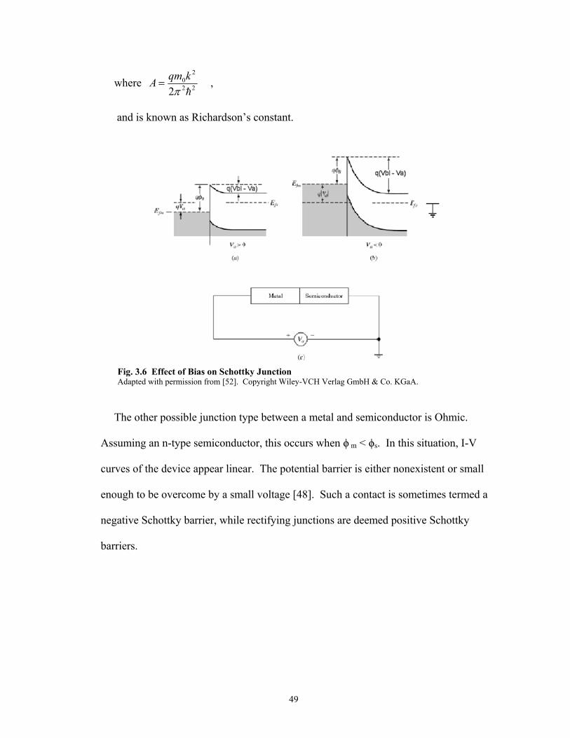
where 22
20
2 kqm
A ,
and is known as Richardson’s constant.
Fig. 3.6 Effect of Bias on Schottky Junction Adapted with permission from [52]. Copyright Wiley-VCH Verlag GmbH & Co. KGaA.
The other possible junction type between a metal and semiconductor is Ohmic.
Assuming an n-type semiconductor, this occurs when ϕ m < ϕs. In this situation, I-V
curves of the device appear linear. The potential barrier is either nonexistent or small
enough to be overcome by a small voltage [48]. Such a contact is sometimes termed a
negative Schottky barrier, while rectifying junctions are deemed positive Schottky
barriers.
49

Fig. 3.7 Ohmic M-S Junction Adapted with permission from [52]. Copyright Wiley-VCH Verlag GmbH & Co. KGaA.
The real world behavior of metal-semiconductor junctions however differs markedly
from the previous theoretical treatment. For instance, the presence of surface states
(charge states present at a semiconductor surface) in the semiconductor’s bandgap often
causes the pinning of the Fermi level to lie inside the semiconductor bandgap, regardless
of the choice of metal for the junction. This pinning effect thereby forces the Schottky
barrier height to a value that has little relationship to the work function of the metal. Due
to this and other non-ideal effects, a practical method used to form Ohmic contacts is to
heavily dope a thin volume of the semiconductor near the metal contact. The heavily
doped region will ensure that any depletion region formed at the interface will be narrow
enough to allow for the tunneling of carriers through the barrier at small voltages.
3.2.2 Effect on Nanowire-based FETs
Schottky barriers are typically present in nanowire-based FETs and they can
specifically give rise to large contact resistances in series with the nanowire channel that
drastically affect NW-FET performance [51]. Due to the large numbers of surface states
in NW-FETs (previously discussed), nanowires are usually susceptible to Fermi level
pinning and resultant Schottky barriers at the metal contacts.
50

One method that is used to reduce Schottky effects of nanowire FETs is the thermal
annealing of the metal contacts. Thermal annealing is an often used process in planar
FETs that reduces contact resistance by inducing the migration of metal atoms into the
semiconductor in order to create a low-resistance (i.e. high carrier concentration) metal-
semiconductor alloy near and around the contact interface [53]. This process has been
shown to work in a similar manner in nanowire-based FETs. As an example, the use of
annealed Ni contacts to fabricate a Si nanowire-based FET has been shown to
dramatically improve the transistor characteristics [54]. High temperature annealing of
the Ni contacts was used to form a NiSi alloy in the contact region of the nanowire which
reduced Schottky effects and increased Ids currents, as shown in Fig. 3.8.
An additional method used to reduce Schottky contact effects on NW-FETs is by the
proper adjustment of the doping level of the nanowire. Four-point probe test structures
were fabricated to examine the FET characteristics of Si nanowires synthesized with two
different n-doping levels, 500:1 and 4000:1. These ratios represent the Si:P gaseous
precursor ratio. As can be noted in Fig. 3.9b, at high doping levels (500:1), the Schottky
effect at the contacts was negligible to Ids-Vds measurements. However, in Fig. 3.9c, it
can be seen that at moderate doping levels (4000:1); the presence of Schottky contacts
seriously impairs current flow.
This reduction in current flow also serves to reduce the transconductance of the FET.
The expression that describes this reduction is given as follows:
wireDSSin
inex RRRRg
gg
/)(1
Eq. 3.12
51

where gex is the extrinsic (measured) transconductance of the NW-FET, gin is the
intrinsic (extracted) transconductance, Rs and Rd are the contact resistance of the source
and drain (which can be determined if four-probe measurements), and Rwire is the
resistance of the nanowire.
Fig. 3.8 Annealing Effect on NW-FET Performance I-Vg characteristics of a SiNW FET recorded for Vsd= +2 V before and after contact annealing; no annealing and T2=250, 300, 350, 400, 450, and 500 °C with fixed T1=200 °C. Reprinted with permission from [54] . Copyright 2007, American Institute of Physics.
Fig. 3.9 Effect of Doping Level on SiNW FET Contacts a) SEM image of a 4-contact SiNW device. b) Ids-Vds curves of for two-probe (green) and four-probe (red) measurements. Doping ratio of Si NW is 500:1 (Si:P) c) Same as b, except doping ratio is 4000:1. d) Measured (blue) and intrinsic, corrected (red) mobility values. Adapted with permission from [55]. Copyright Wiley-VCH Verlag GmbH & Co. KGaA.
52

3.3 Transistor Analysis
3.3.1 NW-FET Gate Capacitance Estimation
For a NW-FET, the gate capacitance represents a measure of how much control the
gate electrode can exert over the nanowire channel. Higher gate capacitances mean that
gate coupling is more efficient leading to reductions in gate operating voltages and power
savings in practical devices. Due to their non-planar geometry and other unique surface
properties, the gate capacitance of NW-FETs can be challenging to predict.
In the most widely studied device geometry, the back-gated NW-FET (Fig. 3.2), the
gate capacitance may be estimated by using the following formula [56]. Where h
represents the thickness of the dielectric and d represents the diameter of the cylindrical
nanowire.
d
dhC
L
C ri 2
cosh
2
1
0
Eq. 3.13
For geometries where h >> d, the following numerical estimate is appropriate:
d
hC
L
C ri 4
ln
2 0 ,
The above formulas are widely used in electromagnetics to model the capacitance
between a metallic cylinder on an infinite metal plate when the cylinder is embedded in a
uniform dielectric. The conditions when this model is noted to serve as an appropriate
estimate of Ci in an NW-FET are: when the NW possesses doping concentrations greater
than 1017 cm-3, and when the NW is much longer than the dielectric thicknesses -
allowing one to neglect the fringing fields at the source and drain electrodes. In order to
account for geometries where the NW is not embedded completely in dielectrics, and is
53

instead laying on a bare insulator surface, the average between the relative dielectric
constant or the insulator and a vacuum may be taken for εr in the formula. For instance,
for geometries where a NW is laying on a bare SiO2 gate insulator, εr is typically taken to
be (1+3.9)/2 ≈ 2.5.
For back-gate geometries where the gate electrode is a flat plane, the cylinder on a
plane model is a reasonable approximation for the gate capacitance. There are other
device geometries, however, where analytical expressions for Ci do not exist, and finite
element electromagnetic simulation is required. Two such situations that require
simulation are: device geometries where the gate electrode is not a flat plane, but rather
conformally surrounds either all or part of the nanowire; and very short channel lengths
(< 1 µm) where fringing electric fields around the source and drain are not negligible.
Another consideration for Ci estimates is that, owing to surface states and size effects,
nanowires often possess a large depletion region near their surfaces which are electrically
inactive [57]. The existence of a surface depletion region would reduce the predicted
gate capacitance as compared to models which did not take this into account.
To elaborate, as a result of their large surface area to volume ratio, nanowires typically
are greatly affected by surface effects. For instance, the interface state density (Dit)
between silicon nanowires and their native oxide has been found to be ~6 x 1012 cm-2eV-1
which is greatly above the typical value of Dit for planar Si (100) surfaces and thermal
SiO2 which are in the range of 1010 cm-2eV-1. The presence of these surface states in
conjunction with the dielectric mismatch of the nanowire with its surroundings has been
shown to cause deactivation of dopant atoms near nanowire surfaces. Due to this
occurrence, the electrically active radius of the nanowire that contributes to electric
54

conduction (relec) is typically smaller than the physical radius of a nanowire (rphys), as seen
in Fig. 3.10. Practically, this has been shown to cause up to a 50% reduction in
conductivity for a 15 nm Si nanowire [58].
Fig. 3.10 Schematic of Dopant Depletion at Nanowire Surfaces Top, Fermi level pinning at the interface due to surface states is illustrated. Bottom, a diagram of a NW showing how positive surface states attract negative charges from the n-type nanowire and cause donor depletion near the NW surface. Reprinted by permission from Macmillan Publishers Ltd: Nature Nanotechnology [58] copyright 2009.
3.3.2 FET Parameter Extraction
It is necessary to be able to extract standard figures of merit in order to analyze the
performance of FET structures. The following section will give an overview of the
procedure to extract these parameters from FET electrical characteristics.
• field-effect mobility (µfe)
Although the mobility (µ) of carriers is an intrinsic material property of a
semiconductor, such factors such as material growth properties, device geometry,
impurity doping, etc. can seriously impact this value in real-world devices. The preferred
method to determine the mobility of a particular semiconductor used as a channel
material is through direct measurement or simulation of FET structures. The mobility
value which specifically describes the FET operation is denoted as the field-effect
55

mobility (µfe). Please note that while other mobility measurement techniques exist, i.e.
Hall measurements, the term µfe applies specifically to the carrier mobility of
semiconductor materials when utilized in particular field-effect device configurations.
The method to empirically determine µfe relies upon IDS-VGS measurements of a FET.
From an IDS-VGS measurement curve, it is possible to plot gm, the transconductance,
which is defined as:
DSVGS
DSm dV
dIg
An analytical expression for gm in the linear region is found by taking the derivative of
the appropriate expression for IDS (Eq. 3.10):
DSife
m VL
Cg
Eq. 3.14
Alternatively, gm may be extracted in the saturation region by taking the derivative of
Eq. 3.11:
TGSisatfe
satm VVL
Cg ,
,
Eq. 3.15
In these two equations for gm, the field-effect mobility may be empirically extracted
for a FET device under test (DUT) if the channel geometry (L), gate capacitance (Ci), and
the IDS-VGS data are known. The field-effect mobility may be extracted under two
different IDS-VGS measurement conditions. The low-field mobility (µfe) is determined for
small VDS biases in the linear regime of FET operation. This bias condition corresponds
to a low longitudinal electric field in the device. Alternatively, the saturation mobility
(µsat) is found when VDS > VDS,sat and the FET is operating in saturation mode.
56

• subthreshold slope (S)
The subthreshold slope (S) is defined by the following expression which is applicable
to IDS-VGS measurements taken near and below VGS = VT of a FET:
1
10 )(log
GS
DS
dV
IdS
S represents a measure of how fast a FET can switch off as a function of applied VGS.
Although a well-known theoretical treatment of S exists for MOSFETs, there is no
general model to explain the physical contributions of S for NW-FETs. Two factors that
effect S which are unique to NW-FETs and are not present for MOSFET devices are: the
JFET-like operation of the bulk nanowire channel at low VGS, and the presence of
Schottky barriers at the contacts. The subthreshold slope is useful as an empirical
parameter that may be extracted from electrical testing data.
• four-point probe measurements
Due to Schottky contact effects, NW-FETs typically possess large contact resistances
at the source and drain metal contacts which greatly influence IDS behavior and which
were not taken into account in the previous theoretical analysis. A schematic of these
series parasitic resistances is shown in Fig. 3.11. For many NW-FETs, the contact
resistances (RS and RD) may be of the same magnitude as the channel resistance (Rch)
even during On mode operation.
A specific test structure, the 4-probe measurement, is used to quantify RS and RD in
order to discern the intrinsic operating properties of the NW-FET, as depicted in Fig.
3.12. The testing procedure proceeds by first measuring the two-probe resistance of the
innermost wire section. The resistance values obtained from the 2-probe measurement
57

includes RS, RD, and Rch. Next, a four-probe measurement is performed where a known
current is applied to the outermost electrodes while the voltage drop that appears across
the innermost electrodes is recorded. This four-probe I-V measurement allows one to
measure Rch directly. Finally, RS and RD may be extracted by simple subtraction [55].
Fig. 3.11 NW-FET Model with Contact Resistances Included
Fig. 3.12 Four-Probe Test Structure a) Two-probe measurements of a NW, includes contact resistance. b) four-probe measurement, contact resistance values may be extracted out of this measurement.
3.3.3 RF Characterization
• Theory
A theoretical model will now be presented to explain the AC (i.e. RF) performance of
FETs. When a FET is operated under AC conditions, it is necessary to consider
additional device properties which do not significantly affect DC operation. One such
property is the presence of capacitances between the source, drain, and gate regions
which arise from the physical geometry of the device. Since the capacitances negatively
58

affect the AC transistor performance, they are deemed parasitic. A schematic displaying
the most important of these capacitances (Cgs, Cgd) is shown in Fig. 3.13a.
For ease of analysis under AC conditions, a transistor is usually treated as a two-port
network. First of all, a port is defined as a pair of device terminals in which a current can
be measured through, or a voltage can be applied across. A two-port device is simply a
device in which there are two separate ports, one nominally for input and the other for
output [59]. For the rest of the discussion, Port 1 will be called the input port and Port 2
will be deemed the output port. As an analytical aid, it is useful to model a two-port
network as a linear system, where a 2x2 matrix may be used to relate current and voltages
at the input and output together. The individual matrix elements are known as
parameters.
The AC performance of a FET is typically quantified by examining how well the
transistor can amplify small-amplitude AC signals (i.e. small-signals) applied to their
a) b)
c)
Fig. 3.13 AC Models of a FET a) model of a NW-FET including parasitic capacitances. b) two-port common source configuration of a FET (DC biases are not shown). c) two-port, small-signal AC model of a FET in the common source configuration
59

gate terminal. The most common amplifier is the common source (CS) configuration as
shown in Fig. 3.13b, where the transistor is assumed to be DC biased in the saturation
region. The name for this amplifier is due to the fact that the source of the FET is shared
as a terminal for both the input and output ports. In order to model the AC operational
characteristics of the CS amplifier, a discrete, linear circuit model may be used. This is
called a small-signal hybrid-π model (Fig. 3.13c), and it includes the effect of parasitic
capacitances (and resistances).
A commonly used metric to quantify a two-port amplifier’s performance is the h21
parameter. It represents the current gain of the amplifier with the output port short-
circuited, and is thus known as the short-circuit current gain. Please note that this is an
AC short-circuit and does not apply to DC signals. According to Fig. 3.13c, it is defined
as:
0
21
dsvi
o
I
Ih
It is useful to directly measure a transistor’s h21 parameter against an AC input
frequency sweep. A frequency of interest occurs at the point where the short-circuit
current gain to decreases to 1. This frequency is known as the unity current gain cutoff
frequency (fT). By performing circuit analysis on the model in Fig. 3.13c, one is able to
solve for fT [60]:
gdgs
mT CC
gf
2
Eq. 3.16
Another parameter of interest in RF testing is the Maximum Stable Gain (MSG), and it
is defined as:
60

12
21
S
SMSG , if the device is stable (i.e. does not oscillate)
Eq. 3.17
The frequency where the MSG decreases to 1 is known as the power gain cutoff
frequency, fmax.
• Testing
In addition to the DC electrical characterization of a FET, it is also important to be
able to test and model the RF (i.e. AC) electrical properties. For real-world RF testing, a
slightly different device architecture is required for the NW-FET (Fig. 3.14) as compared
to the previously discussed FET schematic (Fig. 3.2). This geometry is called the
Ground-Signal-Ground (GSG) configuration (i.e. a two-finger gate FET design). The
GSG transistor configuration consists of two gated channel regions which share a
common drain electrode. The two channel regions are electrically connected in parallel
in this structure. The purpose of the configuration is to allow for two-port S parameter
testing of the FET. Specifically, the GSG configuration provides RF microstrip shielding
of the high frequency electronic signals required for RF testing.
In order to carry out RF testing, a network analyzer is typically used. The analyzer is
able to measure the S-parameters of a two-port amplifier under test. These S parameters
may be converted, for instance, to parameters of interest such as h21 [61].
61

Port 2
Port 1
S
D
G
S
Gnd Gnd
S
D
G
SS
D
G
S
Gnd Gnd
Fig. 3.14 Ground-Signal-Ground NW Device Structure The labels S, D, and G correspond to the source, drain, and gate electrodes, respectively. The red horizontal lines represent the nanowires used as the channel in the device.
3.4 Summary
In this chapter, the analytical methods for describing the behavior of nanowire-based
field-effect transistors (FETs) were presented. By carrying out a derivation of the
analytical equations describing the bulk conduction and field-effect modulation of
nanowire-based transistors, it was found that under most conditions the approximations
and methods utilized in analyzing MOSFET devices may also be utilized to perform
highly accurate analyses of nanowire-based devices.
In addition, the effect of Schottky contacts on nanowire-based FETs was described in
light of the critical influence that their presence may have on device characteristics.
Lastly, methods to extract the FET parameters at both DC and RF frequency regimes and
common device test structures such as 4-probe or GSG microwave FET structures were
presented.
62

Chapter 4
4 Nanowire Transfer
4.1 Transfer Overview
There are a variety of approaches to achieving the transfer of nanowires from a growth
substrate to a deposition substrate of interest [62]. The transfer approach that meets the
requirements for and was studied in this work is the direct transfer of nanowires by
mechanical shear force. Another name for this method is contact printing or dry transfer.
An overview of the contact printing nanowire transfer method will be presented.
Although this discussion focuses on its particular usage in this thesis work; the method
has been demonstrated on other nanostructures, like carbon nanotubes [63], or for high-
throughput processes via roll-printing [64]. The approach relies upon the simultaneous
application of two forces (van der Waals, and shear force) to carry out the uniaxial
alignment and transfer of nanowires.
A step-by-step overview of the contact printing method will now be presented as
pictured schematically in Fig. 4.1. The transfer sequence will be broken down into three
steps: physical contact, application of shear force, and nanowire breakage. Before the
discussion begins, it is important to describe the starting condition for the nanowires in
any transfer process. After growth, synthesized nanowires are held onto their growth
substrate via a mechanical anchor point at their initial growth site (see section 2.1).
1) First, the nanowire growth substrate and receiver substrate are placed in direct
63

physical contact. As pictured in Fig. 4.2, a weight is attached on top of the growth
substrate in order to exert the proper downward force so as to cause a significant amount
of nanowires to bend and come into direct contact with the deposition surface [65]. At
this point, due to surface interactions and resultant van der Waals forces, the nanowires
will adhere to the deposition surface while simultaneously still being anchored to the
growth substrate. Although it is difficult to theoretically model the exact amount of force
caused by the van der Waals adhesion between the nanowire and the deposition surface,
it has been directly observed and measured in an in-situ SEM experiment for the case of a
ZnO nanowire and a Si substrate [66]. Removal of the applied pressure in this step will
generally result in very few NWs being transferred onto the receiver substrate.
Practically speaking, the strength of the NW anchor site on the growth substrate is
stronger than the NW adhesion to the deposition substrate.
2) Next, a shear force is applied onto the growth substrate. As shown in Fig. 4.2, this
can be accomplished by a moving micrometer that directly pushes against the weight,
resulting in the lateral movement of the growth substrate which is attached to the bottom
of the weight. A shear force is simply defined as the force resulting from the movement
of one object in physical contact against another object. In this situation, the applied
shear forces are between the nanowires and the deposition substrate and are in a direction
parallel to the motion of the moving growth substrate. The applied shear force on the
nanowires will cause them to uniaxially orient themselves in the direction of the shear
force. Please note that in this step, the van der Waals and shear forces are acting on the
nanowires simultaneously and in different directions, downwards and laterally,
respectively. It is important to note that the orientation of the synthesized nanostructures
64

on the growth substrate is irrelevant, the shear forces in this step will force the alignment
of the nanostructures into the applied direction.
3) Eventually, the competing shear and van der Waals forces will cause a critical
amount of stress on the nanowire in a certain region, resulting in the physical breakage
(i.e. fracture) of the nanowire and its detachment onto the target substrate surface.
Typically the fracture point occurs somewhere in the midsection of the nanowire; thereby
resulting in transferred nanowires that are shorter than the original growth length.
After NW transfer, the growth substrate may be lifted off, resulting in a transferred
nanowire ‘film’ on the surface of the receiver substrate (Fig. 4.1c). If the transfer
conditions were optimal, the nanowire film coverage will nearly match the original
contact area between the two substrates (Fig. 4.3a). Additionally, another consequence of
one-to-one nanowire surface coverage is that sharp transitions between areas of high
density nanowire coverage and bare areas may be obtained on the receiver substrate (Fig.
4.3b).
Subsequent to NW transfer, device isolation may be performed by selective nanowire
removal (Fig. 4.1d,e). This may be achieved by photoresist patterning and nanowire
removal either by sonication or etching. TFTs may then be fabricated on the device areas
through conventional semiconductor processing.
65

Fig. 4.1 Nanowire Contact Printing and TFT fabrication a) process starts by synthesizing nanowires on a separate growth substrate. b) the nanowire growth substrate is brought into contact with the desired receiver substrate, a uniaxial shear force is applied which causes nanowire transfer and alignment. c) after transfer, a uniaxially aligned ‘film’ of nanowires is obtained on the receiver substrate. Right, SEM image of transferred SnO2 nanowires on a SiO2 surface. d) patterning of a photoresist masking layer. e) sonication in a solvent solution is performed to detach nanowires, and then photoresist is removed by wet solvents. f) contact electrodes are formed by microelectronic fabrication techniques.
66

Fig. 4.2 Experimental Contact Printing Setup
Fig. 4.3 Images of Transferred Nanowires a) Optical image of a SiO2/Si receiver substrate following NW transfer. b) 500x microscope image of the indicated area in a.
4.2 Contact Printing Optimization
For TFT applications, it is desired that a transferred nanowire film possess nanowires
of sufficient length, orientation, and density so as to maximize the amount of nanowires
that bridge the entire length of the channel region of the TFT. In order to optimize for
these parameters, the effect of various deposition conditions will be detailed.
Generalized trends will be discussed, since the properties of the nanowire growth
67

substrate (i.e. density, diameter, type, and length of the NWs) will differ depending on
the application.
a) b)
Fig. 4.4 Effect of Pressure on Contact Printing a) SEM image of a SiO2 surface after contact printing of ~20 nm diameter core-shell Ge/Si nanowires with low pressure (~5 psi), 3 µm scale bar, b) high pressure conditions (12 psi) with no lubricant, 5 µm scale bar
The applied pressure during contact printing has a critical effect on the transfer of
nanowires. Roughly speaking, low contact pressures lead to low-density nanowire
transfer, while higher pressures tend to cause increased transferred nanowire densities.
Fig. 4.4 displays images of these two regimes. An important consideration of note is that
higher pressures also tend to break nanowires into shorter lengths. Excessive breakage
(and a resultant higher tendency for misalignment) of nanowires has been observed to be
a particular problem for nanowires of diameters less than 50 nm (Fig. 4.4b), and is
presumed to be due to their weaker mechanical strength as compared to thicker
nanowires. Moreover, at even higher pressures, the growth substrate may experience
scratching due to abrasion from microscopic dust particles.
It is thought that the excessive breakage and misalignment of transferred nanowires is
a result of an excess of friction arising from a combination of NW-NW and NW-receiver
68

substrate interactions. A strategy to mitigate these effects is through the use of wet
lubricants during transfer [67]. In general, the purpose of a lubricant is to act as a buffer
medium in order to reduce the friction between two sliding surfaces. Through the proper
use of a lubricant in NW contact printing, the aforementioned sources of excess friction
may be reduced, resulting in longer and straighter transferred nanowires. An image of an
optimized transfer of ~20 nm diameter nanowires is shown in Fig. 4.5b. . An overview
of the optimal conditions found for nanowire transfer is given in Table 4.1.
Table 4.1 Optimal Contact Printing Conditions
Type of NWs Applied Pressure Distance Moved Speed etc
~20 nm Ge/Si 10 psi 0.5 mm 0.3 mm/min
8:1 octane : heavy mineral oil lubricant
~50 nm SnO2 5 psi 0.5 mm 0.3 mm/min
No lubricant used.
The thickness of the lubricant layer must be properly controlled to achieve both high
transfer densities and a reduction in friction. An excessively thick lubricant layer will
cause low transfer densities, while a layer that is too thin will not provide the desired
reduction in friction. The thickness of the lubrication layer may be adjusted by varying
either the lubricant viscosity or applied transfer pressure. Either a lower viscosity
lubricant or a higher transfer pressure results in a thinner lubrication layer [68].
69

a) b)
Fig. 4.5 Optimal Contact Printing Conditions for Nanowire Transfer a) SEM image of ~50 nm diameter SnO2 nanowires. b) ~20 nm diameter Ge/Si core-shell nanowires transferred with the aid of lubricant.
4.3 Gate Capacitance Considerations for Nanowire Arrays
Since the purpose of the transferred nanowire arrays in this work is to serve as the
channel regions in fabricated TFTs, it is important to consider their effect on TFT
electrical performance. In particular, the effect of the nanowire channel region on the
transconductance of a NW-TFT will be examined. Intuitively, one could surmise that as
the nanowire density in the TFT channel region increases, so would the current-carrying
ability of the TFT and in turn its transconductance. Although this relationship is correct,
it is not a linear one, and it depends crucially on understanding how the gate capacitance
of the TFT varies with nanowire transfer density.
Here the term nanowire coverage denotes the ratio of the area covered by the
transferred nanowires which bridge the source and drain electrodes as compared to that of
the physical channel area of the TFT (W × L). In order to predict the effect of varying
nanowire coverages on TFT performance, electrostatic simulations (Fig. 4.6) of a specific
70

NW-TFT device structure were performed. The simulations show that for NW-TFTs
possessing NW coverage of greater than 25% and a 130 nm thick SiO2 gate dielectric,
that the simulated value for the total gate-channel capacitance of the NW-TFT, Cgs, is in
fact within 95% of the value estimated by using the parallel plate model. This result
reveals that when nanowire coverage exceeds 25%, the nanowire arrays are able to
achieve a capacitive coupling between the gate electrode and NW channel that is at least
95% as much as it is for a conventional TFT device. This result can be appreciated by
examining the E-field profile of the simulated NW-TFT in Fig. 4.6a. Note that the E-
field strength near the gate electrode is close to 7.7 MV/m along the entire width of the
channel, i.e. the same E-field magnitude as would be predicted for a conventional TFT
with the same dielectric thickness. Since the TFT transconductance is directly related to
Cgs, one can conclude that increasing the nanowire coverage above 25% will have little
effect on the TFT performance.
The nonlinear relationship between NW-TFT performance and the NW coverage can
be explained by looking at this problem from a different angle. It is instructive to let the
transconductance in the linear regime for a NW-TFT composed of N parallel NWs to be
defined as the sum of N individual NW devices:
dsife
m VL
CNg
2
Eq. 4.1
assuming the nanowires are identical. Here Ci corresponds to the effective gate
capacitance for a single-nanowire.
Please also note the classical definition of a TFT’s transconductance (in the linear
regime), where Cox is the capacitance as predicted by the parallel plate model:
71

dsoxfem VCL
Wg
Eq. 4.2
By comparing Eq. 4.1 and Eq. 4.2, one is able to write a proportional relation, such
that:
oxi CLWCN ~ Eq. 4.3
Thus one can notice that the fixed value of Cox for a given TFT geometry places an
upper bound on N×Ci as N increases. Qualitatively, in the extreme case of very low NW
coverage, Ci is determined by examining the capacitive contribution of each nanowire
separately via the approximately correct cylinder-on-a-plane EM model (Fig. 4.7) and Eq.
3.13 so that the individual Ci value is large but N is small. As NW coverage increases,
the field lines from the gate are shared by more nanowires so the effective coupling to
each nanowire (hence Ci) decreases. Above a certain nanowire coverage, the effects of
increasing N and decreasing Ci almost completely cancel each other, and the
transconductance of the NW-TFT device no longer improves with increased nanowire
coverage.
This observation has important consequences in nanowire-based electronics, as it
shows that nanowire arrays produced using less-than-optimal assembly techniques with
relatively low coverage can still act effectively as thin-film devices. Fig. 4.6b shows the
calculated gate capacitance Cgs as a function of the nanowire coverage, at different oxide
thickness conditions. For relatively thick gate dielectric thicknesses (blue squares) that
can be readily produced with inexpensive, scalable techniques such as sputtering, a
nanowire film with low surface coverage will electronically behave similarly to a
complete planar single-crystalline thin-film of the same material and thickness as the
72

channel in TFT devices. The advantage of a higher coverage (denser) nanowire channel
can only be accessed by using thinner gate dielectric or high-k materials to allow for the
more effective capacitive coupling to the nanowire array (red diamonds, Fig. 4.6b).
a) b)
Fig. 4.6 EM Simulations of a NW-TFT a) Simulated electrostatic potential distribution of a cross-section a NW-TFT with tox = 130 nm, Vapp = 1 V. b) Plot of the gate capacitance of the NW-TFT vs. the percentage of nanowire coverage in the channel region. The gate capacitance is normalized to the maximum possible capacitance when the nanowire coverage is 100% (i.e. a conventional TFT).
Fig. 4.7 E-M Simulations of a Low-Density NW-TFT Simulated electrostatic potential distribution of a cross-section a NW-TFT with the following parameters: a gate insulator with εr=8 and a 25 nm thickness, a nanowire channel consisting of 25 nm diameter NWs at a coverage of 2.5%, and Vapp = 1 V. The normalized total NW-TFT gate capacitance is 9.6% as compared to the continuous thin-film case.
73

4.4 Summary
In this chapter, an overview of the nanowire transfer method known as contact
printing was presented. Under optimal deposition conditions, the method is capable of
producing aligned transfers of uniaxially orientated nanowires at lateral densities as high
as one nanowire per ~1-2 microns. Moreover, by appropriately varying the deposition
parameters (i.e. applied shear force), a variation in the deposited nanowire densities may
be achieved. With the aim of producing the highest density and well-aligned nanowire
transfers, the optimal deposition conditions for nanowires examined in this thesis (SnO2
and Ge/Si core/shell) nanowires were detailed.
Lastly, in order to examine the applicability of such transferred nanowires to
electronic applications, the electrostatic capacitive simulation of a thin-film transistor
(TFT) based upon an array of contact printed, aligned nanowires was performed. In
particular, by examining the effect of lateral nanowire density on TFT performance, it
was shown that nanowire-based transistors fabricated utilizing nanowire densities lesser
than the perfect case of 100% close-packed can still achieve performance levels very near
to the close-packed case for common TFT gate geometries.
74

Chapter 5
5 Single Nanowire Device Characterization
5.1 SnO2 Nanowire FET Devices
Prior to the fabrication of multiple nanowire-based TFTs, the performance of
individual SnO2 nanowire-based transistors was measured. SnO2 nanowires were
examined in this work due to their low growth cost, high optical transmittance (for
transparent applications), and their proclivity to forming Ohmic contacts with either
metallic or transparent conducting oxide (TCO) electrodes. Although there are many
reports in the literature on ZnO [57] and Si [55] nanowire-based FETs, for instance; the
electrical characterization of SnO2 nanowires has not been exhaustively explored.
In this research, single-crystalline SnO2 nanowires were grown using the vapor
transport synthesis method that was previously detailed for metal oxide nanowires. In
previous studies of SnO2 nanowire or nanobelt structures, intentional doping was not
achieved and the carriers (electrons) were provided by deviation from stoichiometry (i.e.
due to the formation of oxygen vacancies) or unintentional doping by (uncontrolled)
impurities in the growth facility [69-71]. The undoped nanowire samples typically
exhibit low carrier concentration and are sensitive to ambient parameters. These
properties, while useful for environmental sensor devices [69], are undesirable in high-
performance transistor device applications. In this work, a reliable in-situ and intentional
doping process was utilized which was shown to dramatically affect the nanowires’
75

electrical properties in a controlled fashion. For instance, degenerately Sb-doped SnO2
nanowires were demonstrated to produce nanowire samples with resistivities as low as
the best Sb-doped SnO2 thin films. In this section (5.1), lightly Ta-doped SnO2
nanowires, which are appropriate for transistor applications, were characterized as the
channel material in nanowire field-effect (FET) and thin-film transistor (TFT) devices.
5.1.1 Defect-induced Carriers in Metal Oxide Semiconductors
5.1.1.1 Effect of Oxygen Vacancies on Carrier Levels
Oxygen vacancies have long been assumed to play a major role in the commonly
observed presence of a significant amount of n-type carriers in many deposited metal
oxide semiconductors; such as ZnO, In2O3, and SnO2 [72]. In this subsection, the effect
of oxygen vacancies on carrier concentration levels will be explained using the Kröger-
Vink notation [73]. This notation is commonly used to describe the charge and positional
states of atoms and defects in ionic crystals. In this notation, superscript x, •, and ′
represents a neutral, positive, or negative charge state, respectively. A double
superscript, such as ′′ may be used to represent a doubly negatively charged species. The
subscript position is used to denote the positional location of the species in the crystal;
possible sites are either atomic or interstitial. The term ‘V’ represents an atomic vacancy.
By analyzing the equilibrium equation for the formation of oxygen vacancies in a
metal oxide, one can discover how such oxygen vacancies can act as doubly ionized
electron donors:
OxO VegOO 2)(
2
12
Eq. 5.1
As can be seen from the above equation, the formation of an oxygen vacancy has
76

the effect of donating two free electrons. Physically, one can visualize the creation of an
oxygen vacancy in a metal oxide by noting that oxygen takes on a 2- charge state when in
an ionic bond in a metal oxide crystal lattice. In order to leave the lattice (as a neutral
diatomic gas), it must give up the 2- charge that it took on while situated in the crystal
lattice.
The physical creation of these unintentional oxygen vacancies is commonly
believed to occur during the metal oxide semiconductor growth. Moreover,
environmental effects may affect the concentration of oxygen vacancies in the
semiconductor post-growth.
Please note that for purposes of thoroughness, many other alternate theories have been
proposed to explain the unintentional presence of n-type carriers. For instance, in the
case of ZnO, both interstitial hydrogen [74] and interstitial Zn [75] have been proposed as
alternative origins for the unintentional n-type doping behavior. These alternate theories
however will not be examined in this thesis.
5.1.1.2 Extrinsic Doping by Impurity Atoms
Due to the incomplete understanding and controllability of the previously discussed
carrier introduction in metal oxide semiconductors due to the presence of oxygen
vacancies, the intentional doping of such semiconductors has been explored as an
alternative route for achieving conductivity control. The intentional doping method to be
explored in this thesis is the usage of extrinisic impurity atoms to act as substitutional
dopants at metal cation sites.
A wide variety of metallic atoms have been observed to behave as substitutional
cationic dopants in a diverse array of metal oxide semiconductors, such as SnO2, ZnO,
77

and In2O3. In this section, the effect of Ta and Sb as substitutional dopants at the cation
sites in SnO2 nanowires will be examined. According to literature reports, Ta and Sb
have both been determined to act as substitutional impurity donor atoms at Sn sites in
SnO2 thin films [76-77]. The basis for the usage of such extrinsic atoms as substitutional
impurities for Sn has been explored due to the closely sized ionic radii of the three
species: Sn4+ (0.069 nm), Sb5+ (0.060 nm), and Ta5+ (0.064 nm) [77]. Theoretically, it is
believed that when incorporated into the crystal lattice, Ta5+ and Sb5+ replace the native
Sn4+ atoms. This substitution of a Ta or Sb atom in place of a Sn atom thus effectively
causes the donation of a single free electron.
The exact mechanism of the electron donation requires the use of Kröger-Vink
notation chemical equations to explain. The following equation describes the donor
mechanism of Ta atoms in SnO2 and follows the analysis given in reference [78].
)(2
522 252 gO
xOxeTaOTa x
OSn
x = 0 to 5. Eq. 5.2
The most important detail to note is that the incorporation of Ta atoms substitutionally
at Sn sites causes an increase in the concentration of free electrons. Another consequence
that Ta doping may have is to effect the concentration of oxygen vacancies by the
production of filled O sites in the lattice as represented by the term in xOOx Eq. 5.2.
However, this effect depends on growth and environmental conditions and the exact
amount of filled oxygen vacancies due to Ta doping can vary (as represented by the
variable x in Eq. 5.2).
A study on epitaxial grown and single-crystalline Sn1-xTaxO2 films by PLD from
mixtures of pure SnO2 and Ta2O5 powders have been carried out which explores the topic
78

further [77]. It was shown that as the ratio, x, of Ta in the Sn1-xTaxO2 films was
increased, so did the resistivity of the films monotonically decrease. Degenerate doping
levels of Ta in the SnO2 were able to be obtained. At a doping level of x=0.03, it was
established by electrical (resistivity and Hall measurements) and temperature dependent
measurements that over 90% of the dopants were activated and a resistivity of ~1.1x10⁻⁴
Ω•cm and carrier concentration of 7.6 x 10²⁰ was achieved.
5.1.2 Experimental Method and Results
The SnO2 nanowires were synthesized on (100) Si substrates by a catalyst mediated
self-catalytic vapor-liquid-solid (VLS) process as described in section 2.4.5.2
(modifications to the method described in this section are detailed below) , in which the
Ta and Sn source materials were provided by a vapor transport method. Briefly, high
purity (99.99%) powders containing the source materials (Sn and Ta, 95:5 wt. ratio) were
first mixed thoroughly and loaded in an alumina boat. (100) Si growth substrates were
sputter-deposited with 5 nm of Au film serving as the catalysts in the VLS process, and
were placed on top of the boat. The alumina boat was then loaded into an alumina tube
positioned inside a horizontal tube furnace. During growth, the furnace was heated from
room temperature to 900 ºC at a rate of 20 ºC/min under Ar flow (500 sccm) with a trace
amount of oxygen. The growth time was 1 hour at 900 ºC, followed by cool down to
room temperature at a rate of 5 ºC/min.
Fig. 5.1a shows a low-magnification scanning electron microscopy (SEM) image of
the as-synthesized sample. The nanowires possess a mean lateral size of 55 nm and a
length that is typically tens of microns long. Structural properties of the nanowires were
further investigated with transmission electron microscopy (TEM) studies. Fig. 5.1b
79

shows a low-magnification TEM image of a single Ta-doped SnO2 nanowire with lateral
size of 50 nm, illustrating a uniform lateral size without obvious tapering along the
growth direction. The crystallography of the nanowires was studied by select area
electron diffraction (SAED) (upper inset, Fig. 5.1b) and HRTEM imaging (lower inset,
Fig. 5.1b). These results show that the SnO2 nanowires have a tetragonal rutile crystal
structure (a = 0.47 nm, and c = 3.18 nm), which is consistent with their single-crystal
structure. HRTEM studies also verify that each SnO2 nanowire is a perfect single-crystal
with no visible dislocations and amorphous surface overcoating. The growth direction of
the Ta-doped SnO2 nanowire shown in Fig. 5.1b was estimated to be [101] based on the
analysis of the diffraction pattern.
Fig. 5.1 Images of as-grown SnO2 nanowires a) Zoomed out SEM image of the nanowire growth substrate displaying high-density growth, scale bar: 2 μm. b) a low-magnification TEM image of a single SnO2 nanowire with the sectional size of about 40 nm. Top inset is the select area electron diffraction (SAED) pattern of the SnO2 nanowire, and bottom inset is a HRTEM image the SnO2 nanowire.
After growth, the nanowires were transferred to various substrates and a number of
device structures were fabricated and tested. Unless noted otherwise, all electrical
measurements were carried out in air at room temperature. Single-nanowire based field-
effect transistors (FETs) with a standard back-gated structure were studied first to
investigate the intrinsic electrical properties of the doped SnO2 nanowires. The device
80

fabrication procedure involves removing the nanowires from the Si growth substrate by
sonication in isopropyl alcohol, and nanowire deposition onto a degenerately doped n+
silicon substrate capped with a 50 nm silicon dioxide (SiO2) layer by drop drying.
Photolithography was then used to define pairs of source/drain electrodes to contact each
nanowire, followed by the metal deposition of Ti/Au (10 nm/100 nm) by electron-beam
evaporation to complete the device structure with the n+ Si substrate serving as the back
gate (Fig. 5.2a).
Fig. 5.2 Transfer characteristics of a back-gated Ta-doped SnO2 nanowire FET a) Diagram of the device. b) Current (Ids) vs. Voltage (Vgs) curve in log scale at Vds = 1V, S = 270 mV/dec. c) Current (Ids) vs. Voltage (Vds) curve with Vgs = 6 V to -4 V in 2 V steps. d) Current (Ids) vs. Gate Voltage (Vgs) curve at Vds = 1V, µfe is estimated to be 121 cm2/(V·s). Inset, SEM image of the device, scale bar is 2 µm.
81

Fig. 5.3 Extraction of Average Mobility Histogram of the extracted field-effect mobilities (µfe) for 75 SnO2 NW FET devices, average mobility is be 156 cm2/(V·s).
The SnO2 nanowire FET shown in Fig. 5.2 exhibited standard n-type transistor
behavior, consistent with effective Ta-doping. The light doping of the SnO2 nanowire
also helps to reduce contact resistance, as evidenced by the apparent absence of Schottky
behavior in the current-voltage (Ids-Vds) characteristics (Fig. 5.2c). In contrast, control
experiments on SnO2 nanowires grown without any extrinsic doping show pronounced
Schottky behavior, consistent with earlier studies (Fig. 5.4) [69-70]. Please note that the
Fig. 5.4 Electrical characterization of a typical undoped SnO2 nanowire device in air. The Ids-Vds characteristics show a low current level and Schottky barrier behavior. VGS = 3 V, 1.5 V, 0 V, -1.5 V, and -3 V from bottom to top. Inset: SEM image of the device. Scale bar: 5 μm.
82

pronounced Schottky effects (i.e. contact resistance) make estimation of the concentration
of carriers (due to oxygen vacancies) from electrical measurements difficult and will not
be attempted.
The field-effect mobility of the device in Fig. 5.2 was estimated using the equation
dsife
m VL
Cg
in the linear regime
Here gm = dIds/dVgs is the transconductance measured in the linear region, L = 4.95
µm is the channel length of the nanowire device. Ci is the capacitance of the back gate
per unit length and can be estimated by utilizing the cylinder on a plane model:
d
dhC
L
C ri 2
cosh
2
1
0
Eq. 5.3
where ε0 is the vacuum dielectric constant, h (50 nm) is the thickness of the SiO2
layer, and d (87 nm) is the lateral size of the nanowire, ε r is the relative dielectric
constant and was chosen to be 2.5 - the average of air (1) and SiO2 (3.9). The estimated
capacitance value of 100 aF/µm also agrees well with results obtained from finite element
simulations. The field-effect mobility of the device in Fig. 5.2 was estimated to be 120
cm2/(V·s) in the linear bias region. The maximum transconductance for this device in
saturation was found to be 2.94 µS at Vds = 10 V. In Fig. 5.3 is a plot of the histogram of
the extracted µfe for 75 devices, with an average µfe value of 156 cm2/V·s. These values
are also consistent with those obtained in single-crystalline SnO2 thin-films [79], and
other metal-oxide nanowires [80].
Please note that the effect of contact resistance on the effective field-effect mobility of
these devices was neglected in these studies. As a result, the extracted mobility values
for the individual SnO2 nanowire-based devices can be expected to provide a lower-
83

bound value for the intrinsic carrier mobility of the semiconductor material.
The carrier concentration (due mostly from extrinsic n-type doping) of the nanowire
shown in Fig. 5.2 can be estimated from Ids-Vds measurements at a certain gate bias, Vgs,
using Eq. 5.4.
nq n
1
Eq. 5.4
At Vgs = 6 V, the nanowire in Fig. 5.2 possesses a resistivity (ρ) of 4.4×10⁻² Ω·cm and
in
as transparent devices, the
fab
the
strate show a transmittance of ~ 80% in the visible light range
of
turn an n-type carrier concentration (n) of 1.2×1018 cm-3.
To demonstrate the potential of Ta-doped SnO2 nanowires
rication of nanowire transistors on glass substrates in which the back-gate, source and
drain electrodes were replaced with transparent conducting Sn-doped In2O3 (ITO) films
(Fig. 5.5a). Briefly, an ITO film with thickness of c.a. 250 nm was first deposited on a
glass substrate (Fisherbrand, 2.5 cm × 2.5 cm, 250 µm thick) by pulsed laser deposition
(PLD) at 400 °C, followed by the SiO2 gate dielectric layer (75 nm thick) deposition via
plasma enhanced chemical vapor deposition (PECVD). Single-nanowire transistor
devices were then fabricated on the SiO2/ITO/glass substrate in the same fashion as
device in Fig. 5.2, except that the source/drain electrodes were replaced by 200 nm thick
PLD deposited ITO films.
The devices on glass sub
380-800 nm. Significantly, no device degradation was observed on these transparent
devices fabricated on glass substrates with transparent ITO electrodes. As seen in Fig.
5.5b, linear Ids-Vds behavior was still observed at small bias, indicating Ohmic contacts
with ITO S/D electrodes. Hard saturation was once again observed at high bias for the
transparent FET, with a saturation transconductance gm = 2.27 µS measured at Vds = 10
84

V. The on/off ratio and subthreshold slope S were inferred from Fig. 5.5c to be 105 and
312 mV/dec, respectively. The field-effect mobility, µfe, was estimated to be 176
cm2/V·s in the linear region. These values are consistent with those obtained on de
fabricated on silicon substrates with Ti/Au S/D electrodes, and clearly demonstrate the
potential of SnO2 nanowires as the basis of fully transparent transistor devices.
The discrepancy between the threshold voltage (VT) of the ITO and metal co
vices
ntacted
de
5.2 Degenerately Doped Metal Oxide Nanowires
In order to demonstrate the flexibility of the in-situ doping of vapor-solid grown metal
vices is due to hysteretic effects during device measurement and will be discussed at
length in section 6.3.
Fig. 5.5 Back-gated Ta-doped SnO2 nanowire FET fabricated on glass with ITO contacts. a) schematic of the device. b) Current (Ids) vs. Voltage (Vds) curve with Vgs = 6 V to -8 V 2 V insteps. c) Current (Ids) vs. Gate Voltage (Vgs) curve at Vds = 0.1 V, S = 312 mV/dec, µfe is estimated to be 176 cm /(V·s). d) SEM image of the device, scale b r is 2 µm. 2 a
85

oxide nanowires, degenerately doped SnO2 and In2O3 nanowires were synthesized and
ch
2
wth and characterization of single-crystalline, degenerately Sb-doped
ssed. To study the electrical properties of the TAO
na
vapor
c
o
aging (inset), the
res
aracterized.
5.2.1 Sb-doped SnO Nanowires
First, the gro
SnO2 (TAO) nanowires will be discu
nowires, devices composed of individual nanowires were prepared according to
previously outlined methods for the fabrication of nontransparent NW-FETs. A mixture
of Sn and Sb metal powders (95:5 wt. ratio) was used as the source material for the
transport growth. Of the more than 100 devices tested, a linear current (Ids) versus
voltage (Vds) curve (Fig. 5.6a) was observed in all measurements on samples defined by
photo- as well as e-beam lithography methods, indicating that low resistance, Ohmi
contacts were readily obtained between the TAO nanowires and Ti/Au electrodes. The
effects of the contact resistance were further studied in four-probe measurements. As
shown in Fig. 5.6a, the I-V curve obtained from the 4-probe method is almost identical t
that obtained from the 2-probe method using the inner pair of electrodes. The contact
resistance was estimated to be 40 Ω for this device, which is much smaller than the NW
resistance (~ 5 kΩ) and can be safely neglected. The ability to reliably obtain Ohmic
contacts with low contact resistances is very desirable for nanoscale devices, and allows
the following discussion to focus on simpler 2-probe device structures.
From the measured resistance value of the device in Fig. 5.6a and the lateral size (63
nm) and the length (1.3 µm) of the TAO nanowire measured by SEM im
istivity of the TAO nanowire was calculated to be 1.53×10⁻³ Ω·cm. For comparison,
the resistivity of an individual undoped SnO2 nanowire was measured to be 0.21 Ω·cm in
86

vacuum in a separate report [81]. The resistivity of undoped SnO2 NWs also depends
strongly on the growth conditions and the presence of ambient gases during testing. In
control experiments, the resistivities of undoped SnO2 nanowires were estimated to be
the range of 10-100 Ω·cm in vacuum (not shown). The much reduced resistivities in the
TAO nanowires is thus indicative of effective Sb doping. The resistivities of more than
100 TAO nanowires were measured and plotted in
in
wire device when
fab the
me,
ith
.7b, the resistivity of the TAO nanowire increased
lin l
Fig. 5.6b. All TAO nanowires show
resistivity values smaller than 1×10⁻² Ω·cm. Significantly, the median resistivity value,
1.92×10⁻³ Ω·cm, and the lowest resistivity value, 4.09×10⁻⁴ Ω·cm, are comparable to the
best values achieved in high-quality Sb-doped SnO2 films [82].
Degenerate doping of the TAO nanowires was further confirmed by a number of
studies. Fig. 5.7a shows the transfer curve, Ids-Vgs of a TAO nano
ricated on a 50 nm SiO2 / n++ Si substrate. Due to the high carrier concentration,
current Ids changed by only 5% when Vgs was varied from +6 to −6 V. In the meanti
the electron mobility for this single-crystalline TAO nanowire was estimated from the
slope of the transfer curve to be 41.9 cm2/V•s. The electron density was estimated using
Eq. 5.4 and found to be 3.06×1020 cm−3. The high carrier concentration is consistent w
the low resistivity of 4.88×10⁻⁴ cm−3.
Temperature-dependence measurements on the TAO nanowires further verified their
metal-like behavior. As shown in Fig. 5
early from 1.59×10⁻³ to 1.74×10⁻³ Ω•cm from 300 to 480 K. This behavior agrees wel
with the linear resistivity-temperature relationship at high temperatures for a metal when
scattering is dominated by electron-acoustic phonon scattering [83].
87

Fig. 5.6 Degenerately Doped TAO NWs a) Comparison of the current-voltage (Ids-Vds) characteristics of an individual TAO nanowire device using four-probe and two-probe configurations. Inset, SEM image of the TAO nanowire device. Scale bar: 2 µm. b) Histogram of the resistivities measured over 100 TAO nanowire devices.
Fig. 5.7 Electrical Characteristics Degenerately Doped TAO NWs a) Transfer curve Ids-Vgs of a TAO nanowire device measured at Vds=100 mV. Inset: SEM image of the device. Scale bar: 2 μm. b) Dependence of the resistivity ρ on temperature T measured in the high-temperature range 300–480 K, showing the expected linear ρ -T behavior.
88

5.2.2 Sn-doped In2O3 (ITO) Nanowires
In order to realize even lower resistivity values, degenerately Sn-doped In2O3 (ITO)
nanowires were investigated. ITO is a widely used thin film transparent conducting
oxide (TCO). Studies on thin-films of ITO have shown that Sn acts as a substitutional
impurity dopant for In atoms in the lattice [84]. Each Sn dopant atom is believed to
donate one electron; the valence states of the metal atoms in the lattice are In3+ and Sn4+.
The entire experimental approach proceeded in a similar manner as previously detailed.
One change of note is that the thermally evaporated source materials for the ITO
nan
T O
nanowires. From the measured resistance value of the device in Fig. 5.8a and the cross-
section size (75 nm) and the length (1.8 µm) of the ITO nanowire (measured by SEM
imaging), a resistivity value of the ITO nanowire to be 9.18 x 10⁻⁴ Ω·cm. The contact
resistance of this device was found to be 55 Ω, which can be neglected as compared to
the total two probe resistance value of 2984 Ω. The resistivities of about 40 ITO
nanowires were obtained and plotted in Fig. 5.8b. Significantly, the median resistivity
val -4 -5 Ω·cm, are comparable to
the an
those reported for ITO nanowires in earlier studies [86].
owires consisted of a mixture of I and SnO powders (90:10 wt. ratio).
wo and four probe device structures were fabricated as well for the grown IT
n
ue 7.15 x 10 Ω·cm, and lowest resistivity value 6.29 x 10
best values achieved in high-quality ITO films [85] and are several orders better th
89
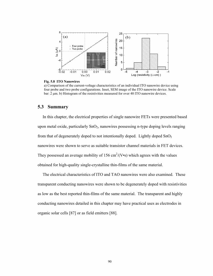
5.3 Summary
In this chapter, the electrical properties of single nanowire FETs were presented based
upon metal oxide, particularly SnO , nanowires possessing n-type doping levels ranging
from that of degenerately doped to not intentionally doped. Lightly doped SnO
nanowires were shown to serve as suitable transistor channel ma .
They possessed an average mobility of 156 cm2/(V•s) which agrees with the values
obtained for high-quality single-crystalline thin-films of the same material.
The electrical characteristics of ITO and TAO nanowires were also examined. These
transparent conducting nanowires were shown to be degenerately doped with resistivities
as low as the best reported thin-films of the same material. The transparent and highly
conducting nanowires detailed in this chapter may have practical us
2
2
terials in FET devices
es as electrodes in
organic solar cells [87] or as field emitters [88].
Fig. 5.8 ITO Nanowires a) Comparison of the current-voltage characteristics of an individual ITO nanowire device using four probe and two probe configurations. Inset, SEM image of the ITO nanowire device. Scale bar: 2 μm. b) Histogram of the resistivities measured for over 40 ITO nanowire devices.
90

Chapter 6
6 Transparent n-type, SnO2 NW-TFTs
6.1
I nO2
nanowire-based TFTs (NW-TFTs) is presented. The NW-TFTs possess DC performance
ingle-crystalline metal oxide TFTs and importantly operate at
frequencies above 100 MHz with tightly dist
2
a
Pyrex glass substrate an
2
Fig. 6.1a). The 75
nm iO2 gate dielectric was deposited by PECVD at 200 ºC and at a rate of 600
nm/min. The highest temperature used during fabrication was limited to below 250 ºC. A
two finger interdigitated design (Fig. 6.1a) was chosen in this study to facilitate RF
Overview
n this chapter, the DC and RF electrical characterization of transparent, n-type S
levels comparable to s
ributed performance metrics among different
devices.
The Ta-doped SnO nanowires utilized as the channel material were synthesized on
(100) Si substrates using a vapor transport method as previously detailed in section
2.4.5.2. One modification to the growth process was the use of 50 nm Au nanoparticles
as the catalyst instead of an Au film. After growth, the nanowires were transferred to
d formed a film composed of aligned nanowires using a contact
printing method following previously outlined methods (section 4.3, see optimized
contact printing conditions). Transparent NW-TFTs were then fabricated using the SnO
nanowire film as the transistor channel and sputtered indium-tin-oxide (ITO) as the
source/drain and gate electrodes in a staggered top-gate geometry (
-thick S
91
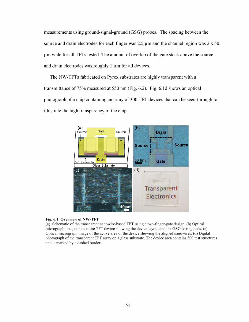
measurements using ground-signal-ground (GSG) probes. The spacing between the
ource and drain electrodes for each finger was 2.5 µm and the channel region was 2 x 50
m wide for all TFTs tested. The amount of overlap of the gate stack above the source
and drain electrodes was roughly 1 µm .
The NW nt with a
transmittance of 75% measured at 550 nm (Fig. 6.2). Fig. 6.1d shows an optical
ip containing an array of 300 TFT devices that can be seen-through to
illus
s
µ
for all devices
-TFTs fabricated on Pyrex substrates are highly transpare
photograph of a ch
trate the high transparency of the chip.
Fig. 6.1 Overview of NW-TFT (a) Schematic of the transparent nanowire-based TFT using a two-finger-gate design. (b) Optical micrograph image of an entire TFT device showing the device layout and the GSG testing pads. (c) Optical micrograph image of the active area of the device showing the aligned nanowires. (d) Digital photograph of the transparent TFT array on a glass substrate. The device area contains 300 test structures and is marked by a dashed border.
92

Fig. 6.2 Transmittance Measurements of the NW-TFTs
6.2 Electrical characterization: DC and RF
Fig. 6.3 shows the Ids-Vds family curves and transfer (Ids-Vgs) characteristics of a
typical device (device A) used in this study. The gate sweep of the device in the
saturation region (Vds = 6 V) showed a large on-current of 2.7 mA (27 mA/mm) and a
peak DC transconductance of 608 µS (6 mS/mm) (Fig. 6.3) with a peak saturation field-
effect mobility of 210 cm2/V·s (assuming a parallel plate capacitance model). As
discussed in section 4.3, due to the high NW coverage in the channel region (estimated to
2 NW-TFT, see Fig. 4.3) and the relatively
ure.
the NW-TFTs using on-chip small signal S parameter measurements. The RF
easurements circumvent problems associated with DC characterizations such as the
presence of mobile charges or surface states and questions in deriving mobility values for
nanowire and nanotube based electronics [89], and unambiguously attest to the NW-
be 25-50% in the channel region for this SnO
thick insulator thickness, the parallel plate model is appropriate for this device struct
In the following section, the discussion focuses on the direct RF characterization of
m
93

TFTs’ viability as high speed electronic devices. The two-port S parameters of the NW-
TFTs were measured using an HP 8751A network analyzer and GSG probes (GGB
Industries, 150 µm pitch) over a frequency range of 1 to 500 MHz. Before
measurements, calibration was carried out using the short-open-load-thru (SOLT) method
and an impedance standard substrate (GGB Industries) to define the reference plane at the
probe tips. The current gain, |h21|2, and maximum stable gain (MSG), |S21/S12|, of the
TFT devices were then extracted from the S parameter measurements at fixed gate and
drain bia
Fig. 6.4a shows the current gain and MSG as a function of frequency for device A.
rent gain and MSG curves can
be well fitted using the ideal 20 dB/dec roll-o
as com
ses without de-embedding.
The TFT was biased at Vds = 6 V and Vgs = 2 V. The cur
ff slope (dotted lines). The unity current
gain cut-off frequency fT was estimated to be 35 MHz, and the power gain cut-off
frequency fmax was estimated to be 110 MHz. These values represent the highest
operation speed reported for transparent electronics to date, and are significantly higher
compared with previous studies on organic semiconductor and conventional TOS thin-
film based TFTs [90-92] .
A key advantage of the NW-TFT approach is that the large number of nanowires that
make up each TFT help to suppress the performance variations among separate devices
pared to transistors based upon a single nanowire. The main device uniformity
concern in the NW-TFT approach is the unavoidable fluctuation of the nanowire density
at different locations and the resulting fluctuation of the number of nanowires that bridge
the channel region in separate NW-TFT devices. However as previously discussed,
simulations suggest that the TFT performance can be insensitive to nanowire density
94

fluctuations above a certain coverage for a given device geometry. The RF
characteristics of an extensive number of TFTs were measured in order to examine
whether the predicted high degree of uniformity would hold true experimentally.
(Vds =
it
ith an average of 34.3 MHz and a standard deviation of only
3.7
T
ce A
of
Fig. 6.4b shows a histogram of the extracted fT values for 39 NW-TFT devices
fabricated using identical processes. All devices were biased at the same voltages
6 V and Vgs = 2 V) and no manual adjusting of the working points was performed. All
devices measured show characteristics similar to those of device A and the fT data exhib
a very narrow distribution w
MHz. The narrow distribution clearly demonstrates that high device uniformity can
be obtained even in the presence of nanowire density fluctuations, and paves the way for
the design and application of high-performance integrated circuits based on the NW-TF
approach.
Finally it is noted that higher operational frequencies may be achieved at larger DC
biases of the TFTs. Fig. 6.5a shows the current gain and MSG vs. frequency for devi
at a higher bias of Vds = 11 V and Vgs = 10 V. A least square fit using a roll-off slope
Fig. 6.3 DC Characteristics of a Transparent SnO2 NW-TFT (a) Family of Ids-Vds curves of device A. (b) Transfer characteristics of device A measured at Vds = 6 V.
95

20 dB/dec (dotted lines) yielded fT = 109 MHz and fmax = 286 MHz for the c
and MSG, respectively. The bias dependence of fT was plotted in Fig. 6.5b. At a fix
gate voltage Vgs = 10 V, fT initially increases monotonically with the drain voltage
urrent gain
ed
until
gain saturation is reached around Vds = 11 V, likely due to the increase and saturation of
the transconductance as the TFT moves from the linear region to saturation region with
increasing Vds (VT ~ 0 for this TFT device, Fig. 6.3).
f these effects is most likely either mobile charges or traps in the oxide itself
or
Fig. 6.4 RF characterization of transparent NW-TFTs. (a) Frequency dependence of the current gain (|h21|
2) and MSG (|S21/S12|) of device A measured at V = 6 V and V = 2 V. (b) Histogram of the extracted f values for 39 devices measured at the ds gs T
same bias conditions.
It is necessary to point out, that although the RF characteristics of the NW-TFTs show
a nearly ideal behavior, their DC characteristics do not. Specifically, the fabricated NW-
TFTs display a hysteresis and sweep speed dependence in their Ids-Vgs testing curves.
The cause o
surface states located at the interface between the nanowire and the gate dielectric.
Such effects on DC measurements are consistent with results from other nanowire-based
transistor devices [10, 93]. In particular, an important property of interface states and
96

mobile charges are that they are typically slow-acting and can only be observed at DC or
low frequency [94]. A consequence of these effects on the testing of DC transistor
performance is that unreliable parameters, such as gm or VT, may possibly be extracted.
Specifically, the value of either of these parameters may depend on the sweep direction
or speed of an Ids-Vgs measurement and may not be fully related to the intrinsic physical
properties of the device. Due to this uncertainty and t
he presence of such hysteretic
effects on the DC characteristics, correlation between the NW-TFT’s DC and RF
parameters (i.e. fT and gm in Eq. 3.16) was only attempted after addressing the hysteresis
problem as discussed in the next section.
Fig. 6.5 RF Characterization, cont. (a) Frequency dependence of the current gain (|h21|
2) and MSG (|S21/S12|) of device A measured at Vds = 11 V and Vgs = 10 V. (b) fT as a function of Vds at a fixed gate voltage Vgs = 10 V.
97

6.3 NW-TFT Optimization and Circuit Applications
Although high-speed operation was observed in direct RF measurements of the
transparent NW-TFT described in the previous section, a non-ideal DC characteristic
(resulting from the presence of hysteresis in near-DC electrical measurements) made
direct comparison between DC and RF measurements infeasible. The reason for such
non-ideal DC effects was thought to be due to the usage of an unoptimized PECVD
gate dielectric in the tested transparent NW-TFT devices. To describe this problem
broadly, the characteristics of nanowire-ba
SiO2
sed transistors have been shown to suffer
deleterious effects due to suboptimal gate insulators. Effects such as an unrealistic DC
transconductance or the presence of hysteresis in the Ids-Vgs measurements are two
common observed results of a poor-quality gate dielectric [89]. One particular source of
these deleterious effects has been attributed to the presence of interface states at the
semiconductor-insulator interface which are a result of interfacial material defects.
With the goal of optimizing the NW-TFT fabrication process to sharply reduce the
presence of deleterious interface states, devices employing an optimized PECVD SiO2
diel iO2
films deposited at a slow rate (~6 nm/min) have much better electrical properties (i.e.
improved resistance, reduced interface states) for device applications than SiO2 films
deposited at higher rates [95]. To this end, NW-TFTs were fabricated employing
PECVD SiO2 insulators deposited at a rate of ~13 nm/min and temperature of 250 °C.
Please note that this deposition rate is much lower than the rate utilized for the devices
detailed in the last section (~600 nm/min).
The fabrication details of the NW-TFTs with optimized PECVD dielectrics will now
ectric were fabricated and tested. It has been noted in the literature that PECVD S
98

be described. Please note that all the details are the same as described in section 6.1
ickness was used for
the ture
Al2O3
s
on
e
atches the actual measured value for fT (343
unless otherwise noted. A PECVD SiO2 gate dielectric of 100 nm th
devices. The insulator layer was deposited at a rate of ~13 nm/min and tempera
of 250 °C. Ti/Au (10/100 nm) metallizations were used for the source, drain, and gate
metals for all of the devices to be examined in this section in order to exclude the
possible of effects of contact or interconnect resistance resulting from the use of ITO.
Following device fabrication, a layer of 10 nm thick ALD Al2O3 was deposited over the
entire device to serve as an encapsulation layer and provide protection of the devices
from environmental and atmospheric effects. Electrical testing on the devices in air
showed that the devices possessed reduced hysteretic effects in their near-DC electrical
characteristics (i.e. Ids-Vgs measurements) when capped with the Al2O3 layer. ALD
thin-films are known to be denser than PECVD SiO2 films and are known to provide
superior protection against atmospheric molecules (i.e. moisture) as compared to PECVD
SiO2 films [96].
The electrical characteristics of a typical obtained NW-TFT will now be described a
shown in Fig. 6.6. A maximum DC tranconductance of 151 μS was measured in Fig.
6.6b at a bias of Vds = 6V and at the specific gate bias of Vgs = 5V. An estimate for fT,
the unity current gain frequency, for this device can be found by using the approximati
in Eq. 3.16. An estimate for the total gate capacitance was made by approximating the
nanowires as a complete thin-film with a gate total gate coverage of (100x2.5 μm2) over
the channel region (Width x Length of the device channel) and a gate dielectric constant
of 3.9 as predicted for the PECVD SiO2 dielectric. The estimated value of fT using thes
parameters is 279 MHz and fairly closely m
99

MHz) as measured by direct RF testing to be described next. An overestimate of the
device capacitance may be the cause for the underestimated value of fT when compared
to the actual measured value due to the incomplete nanowire coverage in the channel
region.
Using this same Vds bias, direct microwave testing on the device was performed.
Specifically, the current gain, |h21|2, and maximum stable gain (MSG), |S21/S12|, of the
TFT device was measured. Using these measurements, a value of 343 MHz was directly
obtained for fT, and a value of 1.24 GHz was extrapolated for fmax at the bias values of
= 6 V and Vgs = 5 V. A -19 db/dec rolloff slope was observed for both |h21|2 and the
MSG which are very close to theoretically expected values (-20 db/dec) for both
parameters.
Utilizing a thin-film capacitance model (with the previous mentioned parameters f
this TFT) and DC low-field transconductance measurements, the effective low-field
field-effect mobil
Vds
or
ity for this NW-TFT, μfe, was estimated to be 36 cm2/V·s using Eq.
3.1
r
4. The reason for this lower extracted value for μfe as compared to the transparent
TFT devices in section 6.2 can be attributed to the difference in interfacial and insulato
properties arising to the different deposition conditions of the two PECVD SiO2
dielectrics. Such factors as the presence of interface states or mobile charges in the
dielectric can account for the discrepancy in extracted field-effect mobility [89].
Although the estimated field-effect mobility values are lower for the devices tested in this
section as compared to section 6.2, the superior microwave performance coupled with a
substantial correspondence between the DC and AC performance as expressed by the
fairly close fT estimate (Eq. 3.16) are more attractive properties for real-world TFT
100

applications.
In addition, two other gate insulators were tested in a similar manner: SiO2 deposited
by e-beam evaporation, and SiO2 deposited by both inert and reactive sputtering.
Althoug
h reasonable DC characteristics could be obtained for both sets of NW-TFT
de and
as
g. 6.7) following a similar fabrication procedure as detailed earlier in the
sec
w
e
vices, the RF characterization of these devices differed substantially from the ideal
no reasonable RF performance metrics could be extracted. It is likely that the poor
electric quality of these films, i.e. charge leakage or mobile charges, can explain these
non-ideal results.
Lastly, in order to demonstrate the suitability of the SnO2 NW-TFTs to logic
applications a two-TFT n-type inverter (using the optimized PECVD dielectrics) w
fabricated (Fi
tion. Voltage transfer characteristic (VTC) measurements of an inverter with an 8:1
driver:load ratio, as detailed in Fig. 6.7c, indicate a maximum gain of 1.02 V/V. A lo
hysteretic width of ~0.5 V for a measurement sweep conducted at 1 V/s verifies that th
inverter can operate at near-DC frequencies and that its operation is not substantially
affected by the presence of slow-acting interface states.
101

Fig. 6.6 SnO2 NW-TFT With Optimized PECVD Dielectrics (a) Micrograph of SnO2 NW-TFT with Optimized PECVD dielectrics fabricated on glass. (b) Transfer characteristics of device measured at Vds = 6 V. (c) Family of Ids-Vds curves of device with Vgs = -4 to 6 V in 2 V steps . (d) Frequency dependence of the current gain (|h21|
2) and MSG (|S21/S12|) of device measured at Vds = 6 V and Vgs = 5 V. Dotted lines are linear fits to the rollof behavior.
102

Fig. 6.7 N-type SnO2 NW-TFT Inverter a) two n-type TFT inverter design. b) optical picture of a two NW-TFT inverter, 8:1 drive:load ratio, 12 µm load transistor width, 100 nm SiO2 PECVD dielectrics c) DC inverter characteristics, Vdd = 14V, gain = 1.02 V/V (slope of red line), hysteretic behavior is shown for a single sweep conducted at 1 V/s.
103

Modeling of Circuit Results
ith the goal of trying to model the observed results of the already examined two-
transistor n-type NW-TFT inverter, SPICE modeling of the NW-TFT electrical
characteristics described in this section was undertaken. Specifically, the SPICE
components utilized to model the NW-TFT were based on the SPICE Level 2 MOSFET
model. Using this created NW-TFT model, a reasonable fit of the measured electrical
behavior of the already described NW-TFT using optimized PECVD dielectrics was
obtained. Based off this single NW-TFT SPICE model, the performance of a two NW-
TFT, n-type inverter was predicted. It is important to note that for practical circuit design
situations, SPICE modeling of semiconductors is desired due to the fact that SPICE is a
widely-used piece of modeling software which allows for analysis of a range of
simulation parameters such as noise or temperature effects.
PSp in
Fig. 6.8a. A detailed listing of the SPICE MOSFET Level 2 parameters is given in Table
6.1. Please note that while real-world values were chosen for known device parameters,
i.e. dielectric thickness and channel dimension, other parameter values used in the SPICE
modeling were chosen in order to best fit the experimental data. Specifically, the values
for the following parameters: source and drain resistance, effective channel mobility
(UO), channel modulation parameter (LAMBDA), and threshold voltage (VTO) were all
chosen so as to best model the experimental measurements.
As depicted in Fig. 6.8b,c; The created SPICE model provides for a reasonable fit of
the real-world measured behavior of the previously described NW-TFT (already
W
The specific SPICE software used for modeling in this section was Cadence
ice v. 9.1. A schematic of the SPICE model created for the NW-TFT is pictured
104

de , while although the created SPICE model does not
pro
ulti-
circuit
ed in the
perimentally tested transistor
driver-
tual
erter
scribed in Fig. 6.6). Please note
vide for a perfect modeling of the measured device characteristics; it does provide a
reasonable enough approximation of the device performance so as to facilitate m
transistor modeling and so as to gain insight to the behavior of these NW-TFTs in
configurations.
To this end, a circuit schematic design for a two-transistor, n-type inverter using the
previously described individual NW-TFT SPICE model was created as shown in Fig.
6.9a. Please note that the configuration of this inverter is exactly the same as the
previously described NW-TFT inverter shown in Fig. 6.7a,b. The schematic design for
the two NW-TFT inverter consists of two NW-TFT SPICE models hooked together as
shown in the simple circuit diagram of Fig. 6.7a. The widths of the transistors us
NW-TFT SPICE models were adjusted so as to match the ex
to-load width ratios (8:1).
Although there is some discrepancy of the predicted and actual measured inverter
testing results, qualitatively they share the same features, i.e. low gain and output range.
The inexact match between the predicted voltage transfer characteristic (VTC) vs. the
actual measured results can be attributed to NW-TFT device inconsistencies among the
actual fabricated devices which makes exact performance prediction difficult. The
qualitatively close matching of the predicted NW-TFT inverter performance vs. the ac
measured results (Fig. 6.9) gives theoretical credence that the experimentally measured
VTC of the NW-TFT inverter is indeed realistic.
The low gain (~1 V/V) and low output range (~35% Vdd) of the characterized NW-
TFT inverter can be explained on a theoretical basis by noting that the chosen inv
105

configuration utilizing a load n-type transistor forced into saturation mode is commonl
only recommended to be fabricated using n-type, enhancement mode, load transistors in
classic circuit design textbooks [97]. The ~0 V threshold voltage of the utilized NW-
TFTs is apparently not positive (i.e. enhancement) enough to function properly as the
load element in th
y
e chosen inverter design configuration. This result is confirmed by the
aforementioned SPICE predictions.
106

Fig. 6.8 Spice Simulation of SnO2 NW-TFT a) PSpice schematic of NW-TFT model. b) Family of Ids-Vds curves comparing the modeling results to the actual measured characteristics of the SnO2 NW-TFT detailed in this section. Vgs = -2 to 6 V in 2 V steps . c) Transfer characteristics of model vs. actual measured results.
Table 6.1 SPICE Model for NMOS Component
.model MbreakN-X NMOS LEVEL=2 UO=18 TOX=100E-9 VTO=-1.2 LAMBDA=.05 *$
107

Fig. 6.9 Spice Simulation of SnO2 NW-TFT Inverter a) PSpice schematic of NW-TFT inverter model. b) Voltage Transfer Characteristic comparing the modeling results to the actual measured characteristics of the SnO2 NW-TFT inverter detailed in this section.
6.4
In this chapter, the DC and RF characterization of thin-film transistors (TFTs)
fabricated using arrays of contact transferred SnO nanowires was detailed. Completely
transparent NW-TFTs utilizing ITO metallizations were shown to operate at speeds (fT)
of 100 MHz. By optimizing the deposition conditions of the PECVD SiO2 gate
through the use of metal contacts, operational speeds (fT) in excess of 300
z were reached. A field-effect mobility of 36 cm2/V·s was extracted for such a
device using a conventional thin-film transistor device model. It is important to note that
the examined nanowire-based TFTs were fabricated at a low temperature (maximum 250
Summary
2
in excess
dielectric and
MH
108

ºC). The device performance levels of these NW-TFTs (expressed in terms of field-effect
mobility and fT) exceed the levels of certain other low-temperature TFT channel
materials, like amorphous silicon or organic semiconductors; and may one day be used as
a higher performance replacement for these existing materials.
Additionally, the suitability of these TFTs in logic circuits was demonstrated with the
fabrication of a functional two-transistor inverter. SPICE-based modeling was performed
to interpret the NW-TFT circuit results.
109

Chapter 7
a method to control the threshold voltage of the
device, two different types of Ge nanowire-based TFTs will be presented. Ge/Si core-
shell nanowires will be utilized to fabricate depletion mode NW-TFTs (VT > 0), and B-
doped Ge nanowires will be employed to fabricate enhancement mode (VT < 0) devices.
Please note that all DC electrical testing was carried out in vacuum in this chapter in
order to reduce the presence of mobile ions (commonly induced by water molecules) near
the nanowires.
roup IV based semiconductors were utilized as the nanowire material in this chapter
due to the current lack of methods to synthesize p-type metal oxide nanowires which
possess device performance levels commensurate with the SnO2 nanowires examined in
Chapters 5 and 6 [98].
7.1 Ge/Si Core-Shell TFTs
Ge/Si core-shell nanowires were grown by the VLS growth method using 20 nm Au
catalyst nanoparticles. The growth was carried out using a CVD process according to
previously demonstrated methods [99]. The synthesized nanowires possessed a uniform
Ge core of 20 nm diameter, surrounded by a Si shell of ~3 nm. The Ge/Si NWs are p-
7 p-type, Ge-based NW-TFTs
In the following chapter, the electrical characterization of p-type, NW-TFTs will be
covered. With the aim of demonstrating
G
110

type semiconductors; due to a band-alignment mismatch, holes from the Si shell will act
as carriers in the Ge core. They are an attractive option for electronic devices since there
are no dopants present in the nanowires, thereby avoiding the problem of impurity
scattering and its associated lowering 100]. Lubricated contact printing
was employed t strates under optimal
co
dip
act annealing was performed. ITO was found not to make Ohmic
co
plots of Fig. 7.1, parts a and b, the NW-TFT displays well-
behaved p-type transistor behaviour, with VT ~ 3 V. As already discussed, NW-TFT
e NW density in the channel region. An image of
the
of the mobility [
o transfer the as-grown nanowires to device sub
nditions (see section 4.2).
For the purpose of carrying out RF measurements, a glass substrate was utilized to
fabricate a NW-TFT under similar methods as detailed in section 6.1. The channel
dimensions of the device are the same at W=50 x 2 µm and L = 2.5 µm. The gate
dielectric consisted of 48 nm of ALD Al2O3 deposited at 150 °C. The electrodes of the
TFT were comprised of 100 nm of Ni deposited by e-beam evaporation. A quick HF
was performed before depositing the source and drain electrodes to ensure Ohmic
contact; no cont
ntact, and the issue of optically transparent contacts for this device will be discussed
later.
The DC and RF performance of a Ge/Si NW-TFT is contained in Fig. 7.1. As
evidenced in the DC I-V
performance depends critically on th
typical transfer density for this device is shown in Fig. 7.1d. The average density of
nanowires for this device can be said to be ~0.5 NWs/µm, however there are large
regions of non-uniformity which makes estimation difficult. The transfer density of these
~20 nm diameter Ge/Si is markedly less than the density obtained with ~50 nm SnO2
111
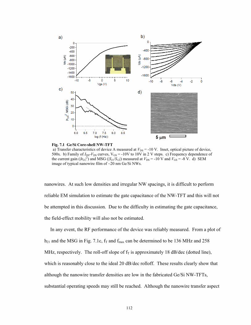
Fig. 7.1 Ge/Si Core-shell NW-TFT a) Transfer characteristics of device A measured at V = -10 V. Inset, optical picture of device, DS
500x. b) Family of IDS-VDS curves, VGS = -10V to 10V in 2 V steps. c) Frequency dependence of the current gain (|h21|
2) and MSG (|S21/S12|) measured at VDS = -10 V and VGS = -8 V. d) SEM image of typical nanowire film of ~20 nm Ge/Si NWs.
nanowires. At such low densities and irregular NW spacings, it is difficult to perform
reliable EM simulation to estimate the gate capacitance of the NW-TFT and this will not
be attempted in this discussion. Due to the difficulty in estimating the gate capacitance,
the field-effect mobility will also not be estimated.
In any event, the RF performance of the device was reliably measured. From a plot of
h21 and the MSG in Fig. 7.1c, fT and fmax can be determined to be 136 MHz and 258
MHz, respectively. The roll-off slope of fT is approximately 18 dB/dec (dotted line),
which is reasonably close to the ideal 20 dB/dec rolloff. These results clearly show that
although the nanowire transfer densities are low in the fabricated Ge/Si NW-TFTs,
substantial operating speeds may still be reached. Although the nanowire transfer aspect
112

requires further optimization, the performance levels of this device structure compare
favorably to literature reports [67, 101].
For transparent electronics applications, an optimization of the electrode contact
materials is required over the previously demonstrated opaque Ni metal contacts. In
order to satisfy the transparency requirements in LED applications, it has been previously
demonstrated that a bilayer contact scheme consisting of a very thin layer of Ni with an
ITO overlayer can serve as an Ohmic contact to semiconductor material [102]. It is
presumed that the higher concentration of carriers in thin metal layer facilitates tunnelling
into the semiconductor material and obviates any noticeable Schottky effects. Due to the
thinness of the Ni metal layer, this film stack still has considerable transparency to visible
ligh e was tested and compared to contacts consisting of
ITO contacts alone.
A two-terminal device consisting of only patterned source and drain contacts was
fabricated on glass to make electrical contact to transferred Ge/Si nanowires under
similar conditions as previously detailed. Two separate contact schemes were examined:
a 100 nm ITO layer, and a 5 nm Ni / 100 nm ITO bilayer. No annealing was performed
on the devices. Testing results for two characteristic devices are shown in Fig. 7.2. As
can be seen, the devices with ITO contacts alone show rectifying electrical behavior,
which is evidence of Schottky contacts. On the other hand, the I-V results for the Ni/ITO
contacts show very linear characteristics. The optical transparency of the Ni/ITO film
stack was determined to be ~50% to visible wavelengths. Furthermore, annealing of the
ITO-only devices did not show any noticeable reductions to the contact resistance.
t. Such a bilayer contact schem
113

Fig. 7.2 Transparent Contacts to Ge/Si NWs Two terminal Ge/Si NW devices on glass, W = 50 µm, L = 2.5 µm. a) I-V testing results from a device employing 100 nm ITO as the contact material, b) a device with 5 / 100 nm Ni/ITO contact material stack
114

7.2 B-doped Ge NW-TFTs
Enhancement mode p-type transistors are an important building block for electronic
applications. For instance, CMOS inverters are typically constructed using enhancement-
mode transistors. In the previous section, depletion mode Ge/Si NW-TFTs were
demonstrated. Although the VT of NW-TFTs employing Ge/Si NW-TFTs may be
adjusted to a small degree by varying either the work function of the gate metal or the
shell thickness [100-101], these methods were not effective to produce enhancement
mode NW-TFT devices due to the large starting VT value. Therefore as a second
approach to obtain enhancement mode operation, B-doped Ge NW-TFTs were fabricated
and
A
followed the procedure in other published reports [21]. B-doping of the nanowire was
achieved by utilizing a process gas mixture of GeH4 and B2H6 gases containing a 4000:1
Ge:B ratio. NW-TFTs were fabricated on a 50 nm thick SiO2/Si substrate where the
degenerately doped Si served as the back gate. Ni films (100 nm) served as the source
and drain electrodes, and were deposited by e-beam evaporation. RTA annealing of the
fabricated devices was carried at 300 °C for 15 s in a 95%/5% N2/H2 gas mixture in order
to reduce contact resistance. As the last step, a 10 nm thick ALD Al2O3 was deposited on
the exposed nanowire surfaces as a passivation layer at 150 °C in order to reduce the
amount of surface states on the NWs. The TFT channel geometry was equal to W = 50
µm and L = 2.5 µm.
The DC electrical testing results of a typical Ge NW-TFT are shown in Fig. 7.3. The
device shows expected p-type transistor and enhancement mode behavior with a VT ~
characterized.
CVD NW growth process was carried out using 20 nm Au nanoparticles and
115

−1.5 V. Similar to the results in the previous section, the NW transfer uniformity was too
ce or mobility estimates. One is able to note that
alt
e
nown
In this chapter, p-type NW-TFTs were fabricated and characterized in terms of DC
and RF electrical characteristics. Specifically, Ge/Si core/shell nanowires were utilized
aterial to realize depletion mode NW-TFTs and B-doped Ge
NWs were used to manufacture enhancement mode p-type TFTs. RF characterization of
irregular to allow for gate capacitan
hough enhancement mode operation was obtained, the transconductance of the device
is approximately 10x lower as compared to the previously discussed Ge/Si NW-TFTs at
comparable bias levels. This reduction in transconductance can be attributed to th
lowering in mobility caused by impurity doping. In addition, Ge surfaces are well-k
to possess a greater amount of surface states in typical device structures as compared to
Si, and this could be another contributing factor [93].
7.3 Summary
as the transistor channel m
Fig. 7.3 Ge NW-TFT testing a) Family of I -V curves, V = -10V to 10V in 2 V steps. b) Transfer characteristics of device DS DS GS
measured at VDS = -1 V. Inset, optical picture of device, 500x. W = 50 µm, L = 2.5 µm
116

the Ge/Si core/shell NW-TFTs confirmed an operational speed (fT) in excess of 100
MHz. These electrical characterization results paired alongside those of the SnO2 (n-
type) NW-TFTs examined in Chapter 6 together represent a basic demonstration of their
device capabilities. The results show that these devices could one day serve as the basis
for complicated circuitry including complementary logic.
117

Chapter 8
8 Conclusion
A few notable experimental results have been accomplished in this work towards the
development of scalable fabrication techniques for nanowire-based electronics. A
practical nanowire transfer method, contact printing, has been demonstrated to achieve
the transfer of dense, aligned nanowire arrays on device substrates, specifically glass. A
large number of individual NW-TFTs, fabricated from these nanowire arrays, were
characterized and were found to operate at speeds (fT) in excess of 300 MHz.
Importantly, devices demonstrated were totally transparent thus establishing the future
applicability of NW-TFTs for the fabrication of transparent electronics. Another
substantial result was the successful demonstration of both n-type and p-type transistors,
opening up the possibility of nanowire-based complementary logic devices.
Moreover, the achieved performance levels of metal oxide NW-TFTs were validated
by comparison with the electrical testing results of single-crystalline ZnO TFTs which are
discussed in Appendix A. The conventional ZnO TFT structure was found to possess a
field-effect mobility (µfe) of ~30 cm2/(V·s) while a SnO2 NW-TFT was estimated to
operate with µfe in excess of 30 cm2/(V·s). These results show that the use of single-
crystalline materials in metal oxide TFT devices can offer a substantial performance
increase over conventional amorphous silicon or amorphous metal oxide semiconductor
materials to be discussed next.
118

8.1 Comparison of NW-TFT to other materials for flexible and transparent electronics
A variety of materials and deposition methods have been researched for the
evelopment of flexible and transparent thin-film transistors (TFTs). Each material and
its associated deposition method possess its own unique benefits and tradeoffs.
Specifically, such properties as field-effect mobility, on/off ratio, doping, and cost vary
wi
r
ith both
h
rication
FTs are
thr
ver,
for
xcess of 100 cm2/V•s); its higher deposition temperatures
d
dely between these materials. The suitability of NW-TFTs that have been
characterized in this thesis work will be compared against other material systems fo
usage in flexible and transparent electronics applications.
To begin, the properties of the characterized nanowire-based TFTs and devices will be
reviewed. This thesis work has shown that it is possible to fabricate NW-TFTs and
devices with mobilities in excess of 30 cm2/V•s, Ion/Ioff ratios beyond 105, and w
n- and p-type semiconductors all at processing conditions near room temperatures. Suc
a combination of device characteristics is not easily matched by the other TFT fab
methods.
For instance, currently the two most widespread methods for fabricating T
ough the use of amorphous or polycrystalline Si [103-104]. Both materials possess a
couple of important benefits. They may be readily doped with acceptor or donor
impurities during their gas phase deposition process, thus allowing for the fabrication of
TFTs performing as either n- or p-type transistors and with large Ion/Ioff ratios. Moreo
amorphous Si may be deposited at low temperatures ~200 °C. The low deposition
temperature of amorphous Si comes at a cost, however; the typical mobilities obtained
a-Si are fairly low and in the range of 0.1-1 cm2/V•s. Although polycrystalline Si
possesses larger mobilities (in e
119

(greater than 500 °C) is incompatible with many glass or plastic substrates. Anot
method that has been demonstrated to produ
her
ce polycrystalline Si at lower deposition
tem ely
aterial
One detrim
attractive benefits to organic sem
aterials. For instance, the mobility for single-crystalline pentacene has been
characterized to be in ex
2 3 2 3
aterial
peratures is excimer laser annealing. Although this method has been positiv
demonstrated, the costs and low throughput associated with laser annealing are not
attractive to large scale manufacturing processes.
Another method for the fabrication of TFTs has gained widespread research attention
recently; it encompasses the attempts to utilize organic molecules as the channel m
in TFTs [92]. The most commonly researched organic semiconductor, pentacene, has
been characterized to possess mobilities of ~5 cm2/V•s when deposited from a gas phase.
ent however associated with pentacene is that it is a p-type material, there has
been more difficulty finding an n-type organic semiconductor with comparable
performance levels. There are a couple of iconductors,
such as the possibility for low-temperature deposition or solution-based material
synthesis; but their ultimate performance levels may never rival those of inorganic
crystalline m
cess of 35 cm2/V•s, which although is high when compared to
amorphous Si, it does not start to match the mobilities of many single-crystalline
inorganic semiconductors.
Another research topic that is attacking the problem from a different angle is the field
of thin-film oxide-based semiconductors. As previously mentioned, oxide-based
semiconductors (such as ZnO, Sn O , and In O ) possess a high optical transmittance and
mobilities in excess of 100 cm2/V•s in their single-crystalline form [79]. Using a lattice-
matched substrate, an n-type TFT was demonstrated using the single-crystalline m
120

InGaO3(ZnO)5 (IGZO) with field-effect mobilities in excess of 80 cm2/V•s [105].
Although the performance level is high, the requirement of a lattice-match yttria–
stabilized zirconia (YSZ) makes the demonstration not compatible with reasonable c
large-scale fabrication methods. When deposited onto non-lattice matched substrate
such as glass, and in amorphous phases the same m
ost,
s,
aterial, IGZO, possesses lower field-
eff
e
d single-
s are
rom
gle-
r source wafers. The performance of such single-crystalline
de
pon the
ect mobility values, in the range of 10-20 cm2/V•s [90, 106]. Although this
performance level is greater than that of amorphous Si, there has been much difficulty in
finding a well-performing p-type oxide semiconductor. Efforts to grow p-type ZnO hav
so far resulted in films which typically possess mobilities in the range of ~1 cm2/V•s
[107]
An additional technique which has been studied is the stamp transfer of etche
crystalline nanoribbons from source wafers [108]. This method has been demonstrated
on a wide variety of semiconductors; such as Si, GaAs, and GaN. The nanoribbon
typically formed by carrying out the etching and subsequent release of the materials f
single-crystalline wafers by an underetch and PDMS stamp transfer process. The
electrical characteristics of TFTs fabricated on flexible substrates using transferred
nanoribbons have been found to closely match the performance levels of these sin
crystalline materials on thei
vices far exceeds that of the traditionally used thin-film materials, but the nanoribbon
stamp transfer method possesses some associated downsides. The method relies u
use of expensive single-crystalline source wafers which limits the scalability of the
method to large deposition substrate sizes while maintaining reasonable cost levels.
The last material to be reviewed is single-wall CNTs (SWNTs). This material
121

possesses very attractive electrical qualities: SWNTs have a long mean free carrier
and possess field-effect mobilities in excess of 1000 cm2/V•s for transistor structu
micron-scale channel lengths [109]. Using stamp transfer [110] or dielectrophoretic
assembly [111], highly aligned SWNT-based TFTs have been fabricated on flexible
substrates and have been shown to possess field-effect mobilities in excess of 100
cm2/V•s. One associated downside of SWNT-TFTs is the presence of metallic
that are typically grown alongside semiconducting SWNTs in a ratio of 1/3 to 2/3 in most
CNT CVD growth processes. The presence of such metallic SWNTs can serve to reduce
the Ion/Ioff ratios of SWNT-TFTs to below 102. Although the selective burning of the
metalli
path
res with
SWNTs
c CNTs through the use of Joule heating has been demonstrated, the random and
de
ing
.
co long
structive aspects of this method may not be compatible with large-scale manufacturing
processes. Another method used to obviate the effects of metallic SWNTs is through the
use of striped and randomly orientated SWNTs networks as the channel material in
SWNT-TFTs [112]. Due to the effects of a percolating conduction path, the Ion/Ioff ratio
of such SWNT-TFTs has been found to be in the range of 105. The use of percolat
conduction paths comes at the expense of field-effect mobility, however; the
demonstrated SWNT-TFT devices in the research work possessed a µfe of ~80 cm2/V•s
Moreover, although this work was able to demonstrate p-type logic circuits based on
SWNT-TFTs, complementary logic SWNT-TFT - based circuits have not been
demonstrated. Chemical doping methods have been typically used to achieve n-type
operation of SWNT-TFTs, but the compatibility of such doping methods with TFT
encapsulation (which is needed for practical, integrated devices) has yet to be
mprehensively established. In addition, the striping method is only applicable to
122

channel devices with channel length > the CNT length, limiting the speed of such
circuits.
8.2 Future Work
A few major challenges to NW-based electronics need to be addressed. The nanowire
contact printing method is a method in critical need of optimization. Although the
density and uniformity of the transferred nanowire arrays prepared by this method were
sufficient for demonstration purposes, scalable manufacturing processes will require b
of these aspects to be improved. In particular, the contact printing process produced
sparser and more irregular arrays of nanowires for smaller diameter NWs (≤ 20 nm) as
compared to larger diameter NWs (≥50 nm). Further optimization, for instance by the
use of appropriate surface functionalizations, should be examined.
Device fabrication is another area of this work that may be improved upon.
Utilizing micron-level patterning techniques, NW-TFT operation above 300 MHz was
demonstrated. In order to achieve higher operating speeds, shorter TFT chann
and thus tinier patterning dimensions are required. Methods to cope with the issue of
patterning on non-planar nanowire surfaces will need to be addressed at such small siz
lengths. Furthermore, the fabrication of NW-TFTs on flexible substrates, such a
film, should be possible by utilizing the methods of this work. Carrying out the actual
demonstration of such devices could help to show that is feasible to produce high
performance flexible and transparent electronic devices.
Lastly, the successful demonstration of complicated electronic circuits utilizing NW-
oth
el lengths
e
s PET
based devices remains to be achieved. This work has successfully shown that NW-based
123

devices can operate at attractive performance levels at an individual device level, b
integratin
ut
g large number of NW-based devices on a single substrate has yet to be
achieved. An initial attempt has been made with the successful operation of an n-type
transistor inverter; but for practical applications, complementary logic using p- and n-
is required. Methods to achieve accurate control over device
pa
type transistor elements
rameters such as threshold voltage will also need to be improved.
124

Appendix A: Single-crystalline ZnO T
Single-crystalline ZnO TFT
FT
Although the focus of this thesis is on single-crystalline nanowires, it is useful to
compare the performance of nanowire-based devices to TFTs fabricated from single-
crystalline thin-films. This section will focus on the electrical characterization of single-
crystalline ZnO TFTs fabricated on Si substrates. ZnO is a semiconductor of interest due
to its wide bandgap and applicability to optoelectronics. In the past, researchers have
typically only examined ZnO-based TFTs utilizing poly-crystalline or amorphous ZnO
thin-films [107]. However due to their lack of crystallinity, the extracted performance
(i.e. mobility) values of the ZnO material in these reports has been below ZnO’s
theoretical limit. To address this issue, the following work carries out TFT fabrication
and electrical characterization of epitaxial grown, single-crystalline ZnO films.
125

Fig. A.1 TEM image of ZnO film stack a) Cross-sectional TEM image of a 400 nm thick ZnO film on 30 nm Sc2O3/Si. b) STEM image of the Sc O /Si interface after growth. c) HRTEM image of the interface before ZnO growth. d) and e) STEM 2 3
images of the ZnO film and the Sc2O3 buffer layer. Reprinted with permission from [113]. Copyright 2009, American Institue of Physics.
Epitaxial ZnO films were prepared by Prof. Xiaoqing Pan’s group by PLD depositio
(~30 nm) onto (111) p-type Si substrates covered by a 30 nm single-crystalline Sc2O3
buffer layer [113]. Sc2O3 is a high-k insulator and its purpose in this work is to se
n
rve as a
buffer layer to relax lattice strain mismatch between ZnO and the underlying Si substrate.
As shown in Fig. A.1, the single-crystallinity of all layers in the material stack was
confirmed by HRTEM observation. The sample imaged in Fig. A.1 is similar to the
device film stack, with the exception that the ZnO layer is 400 nm thick in the figure.
126

Fig. A.2 TLM measurements of ZnO film Inset, optical picture of TLM structure.
Both back-gated and top-gated TFT structures were fabricated on this substrate. First,
ba
ion
r
this method is shown in Fig. A.2 and Table A.1 and was carried out according to [114].
The TLM measurement setup consisted of 6 electrodes (200 µm wide, 10 µm long) on a
ZnO mesa spaced apart in distances varying from 5 µm to 25 µm in 5 µm increments.
The contact resistivity (ρc) of the Ti/Au contacts to the ZnO film was found to be ~10-4
ck-gated devices using the Sc2O3 layer as the gate dielectric will be discussed.
Fabrication began with device isolation (i.e. mesa) etching; dilute HCl acid was used to
etch the ZnO layer. The Sc2O3 layer was not etched by the acid. Source and drain
contacts were deposited by e-beam evaporation of Ti / Au (20/80 nm). Both long and
short channel devices were fabricated, i.e. L = 20 µm and 5 µm.
In order to establish the contact resistance values for the TFTs, a TLM (Transmiss
Line Method) structure was fabricated via the same process. The extraction process fo
127

Ω•cm2 and compared favorably to literature values [115].
Table A.1 ZnO TLM Measurement Results
DC characterization of a long-channel ZnO TFT with channel dimensions of W = 120
µm, L = 20 µm was performed. Normal n-type transistor behavior was observed and
gate leakage
r 2 3
r fe
sat2/V·s.
The extra fe
fe s
LT (µm) Rc (Ω) Rsheet (Ω/sq) ρc (Ω•cm2)
Vgs= 3 0.952 73.69 1.55E-02 1.40E-04
Vgs= 4 1.190 75.39 1.27E-02 1.80E-04
Vgs= 5 1.220 67.22 1.10E-02 1.64E-04
was negligible (Fig. A.3). The value of the gate capacitance of the TFT was
reliably estimated by directly measuring the value of ε for the Sc O dielectric. C-V
measurements were conducted on MOSCAP structures fabricated on-chip alongside the
TFTs, and ε was found to be ~14. The field-effect mobility (µ ) of this device was
estimated from low-field transconductance measurements and was determined to be 31.3
cm2/V·s. Saturation mobility (µ ) was also estimated and was found to be 28.2 cm
cted value of µ agreed well with Hall measurements of the mobility of the
film.
To further test the electrical properties of the ZnO material, short channel devices
were fabricated with a channel geometry of W = 50 µm, L = 5 µm. DC testing results
reveal in Fig. A.4 that at such channel lengths, short-channel effects (i.e. channel length
modulation) are apparent. In a similar manner to the previous device, the µ value wa
128

estimated to be 30.7 cm2/V·s and the saturation mobility (µsat) was estimated as 31.5
cm
0
nd was carried out at 250 °C. A Ti/Au (20/80 nm) top gate metal was deposited on
top at
2/V·s.
Fig. A.3 Long-Channel ZnO TFT a) schematic of device structure. b) Family of I -V curves, V = -4 V to 4 V in 1 V steps. ds ds gs
Inset, optical picture of device (500x), W = 120 µm, L = 20 µm. c) Plot of Ids-Vgs and its derivative at Vds = 0.1 V. d) Log scale plot of Ids-Vgs at Vds = 0.1 V.
Lastly, a top-gate geometry was fabricated on top of the previously examined back-
gate TFT structure. The top-gate dielectric was deposited by thermal ALD of Al2O3 (3
nm) a
of the dielectric by e-beam evaporation. Ids-Vgs measurements in Fig. A.5 show th
due to the additional fabrication processing steps on the TFTs, a negative threshold
voltage (VT) shift occurred. The VT associated with the bottom gate shifted towards the
negative by ~7 V, and the bottom gate could no longer turn off the device at reasonable
129

bias levels. The origin of this VT shift can be attributed to the removal of chemisorbe
oxygen on
d
the ZnO surface during ALD processing [116]. Since oxygen vacancies act as
an n-type carrier in metal oxide semiconductors, oxygen removal has the effect of
increasing the carrier density in the TFT channel which thereby explains the VT shift. A
thorough understanding of the phenomenon and a means of controlling this threshold
shift are a requirement for the further development of metal oxide based electronics.
Low-field mobility estimates (following the previous procedure) were separately
carried out on both the top and bottom gates of the TFT in Fig. A.5; µfe was determined
to be 49.0 cm2/V•s and 26.5 cm2/V•s, respectively. A possible origin for the discrepancy
between the extracted mobility values for the top and bottom gates could be due to a
difference in interface quality or ZnO film quality between these two regions.
In particular from a materials growth point of view, it is likely that the upper-most
portion of the ZnO film possessed a higher material quality (i.e. fewer defects) as the
portion of the ZnO film closest to the original growth surface effectively acts as a buffer
layer which suppressed the creation of lattice defects in the upper portion of the ZnO
film d to be
the ismatch between single-
cry
. In other words, the initial few nanometers of ZnO growth can be hypothesize
region where most of the defects arising from the lattice m
stalline ZnO and Sc2O3 were concentrated. The experimentally extracted values for
field-effect mobility lend credence to this theory since mobility estimates extracted by
applying top-gate modulation (49.0 cm2/V•s) were conclusively higher than the
measurements taken using the bottom gate (26.5 cm2/V•s). Such findings are consistent
from a device point of view by noting that when a TFT is strongly in the turn-on
condition, the region of the semiconductor layer where accumulated mobile charge is
130
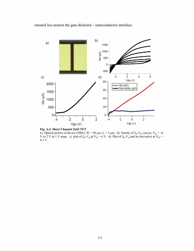
situated lies nearest the gate dielectric / semiconductor interface.
Fig. A.4 Short Channel ZnO TFT a) Optical picture of device (500x), W = 50 µm, L = 5 µm. b) Family of I -V curves, V = -4 ds ds gs
V to 2 V in 1 V steps. c) plot of Ids-Vgs at Vds = 6 V. d) Plot of Ids-Vgs and its derivative at Vds = 0.1 V.
131

Fig. A.5 Top-gated ZnO TFT a) device structure, the Si/Sc2O3 material stack is denoted as the back-gate, and the Au/Ti/Al2O3 stack is denoted as the top-gate. b) Optical picture of TFT, W = 50 µm, L = 7 µm. c) plot o Ids-f Vgs with back-gate voltage as the sweep parameter and a fixed top-gate voltage (Vtop), Vds = 0. V. 1d) plot of Ids-Vgs with top-gate voltage as the sweep parameter and a fixed back-gate voltage (Vback), Vds = 0.1 V.
Summary
With the aim of establishing a basis for comparison of the previously examined metal
oxide nanowire-based TFT (Chapter 6); a TFT based upon a single-crystalline thin-film
of ZnO was fabricated and characterized. DC electrical characterization of both a back-
and a top-gated ZnO TFT was performed. Device testing revealed that a typical top-
gated ZnO TFT possessed an effective field-effect mobility of 49.0 cm2/V·s. When
compared to the best performing PLD-deposited ZnO TFTs in the literature [117], the
extracted mobility values for the devices examined in this Appendix fall somewhat below
the best-in-class value (68 cm2/V·s). The exact reason for this discrepancy is unknown at
132

this stage. It needs to be noted that the mobility levels obtained from the single-
crystalline ZnO film reported in the Appendix work and from the best-in-class ZnO TFTs
[117] are in the same range as the metal oxide nanowire-based TFTs examined in Chapter
6.
It is also important to note that the single-crystalline ZnO TFT examined in this work
also possesses its own merits as an electrical device. Transistors based upon this material
could be useful in high-power applications or optoelectronic applications. Further studies
are required in order to optimize the deposited ALD insulator for top-gated devices in
order to reduce the observed threshold voltage shift which has been commonly reported
as a result of the use of ALD dielectrics in metal oxide-based TFTs. Finally, microwave
testing of the high-frequency performance of single-crystalline ZnO TFTs will be nee ed
to p
d
rovide direct evidence of the high-speed operational potential of these devices.
133

Bibliography
[1]
properties and applications," Mat. Sci. Eng. R-Rep., vol. 52, pp. 49-91, 2006.
[6] A. I. Hochbaum, R. Fan, R. He, and P. Yang, "Controlled Growth of Si Nanowire Arrays for
the Eutectic Temperature," Science, vol. 316, pp. 729-732, 2007. nthesis
[10] D. Wang and H. Dai, "Germanium nanowires: from synthesis, surface chemistry, and assembly to devices," Applied Physics A: Materials Science & Processing, vol. 85, pp. 217-225, 2006.
[11] G. Gu, M. Burghard, G. T. Kim, G. S. Dusberg, P. W. Chiu, V. Krstic, S. Roth, and W. Q. Han, "Growth and electrical transport of germanium nanowires," Journal of Applied Physics, vol. 90, pp. 5747-5751, 2001.
[12] R. Anantatmula, A. Johnson, S. Gupta, and R. Horylev, "The gold-silicon phase diagram," Journal of Electronic Materials, vol. 4, pp. 445-463, 1975.
[13] V. T. Renard, M. Jublot, P. Gergaud, P. Cherns, D. Rouchon, A. Chabli, and V. Jousseaume, "Catalyst preparation for CMOS-compatible silicon nanowire synthesis," Nat Nano, vol. 4, pp. 654-657, 2009.
[14] J. L. Lensch-Falk, E. R. Hemesath, D. E. Perea, and L. J. Lauhon, "Alternative catalysts for VSS growth of silicon and germanium nanowires," J. Mater. Chem., vol. 19, pp. 849 - 857, 2009.
[15] F. Patolsky, G. Zheng, and C. M. Lieber, "Fabrication of silicon nanowire devices for ultrasensitive, label-free, real-time detection of biological and chemical species," Nat. Protocols, vol. 1, pp. 1711-1724, 2006.
[16] K. W. Kolasinski, "Catalytic growth of nanowires: Vapor-liquid-solid, vapor-solid-solid, solution-liquid-solid and solid-liquid-solid growth," Current Opinion in Solid State and Materials Science, vol. 10, pp. 182-191.
[17] H. Adhikari, A. F. Marshall, I. A. Goldthorpe, C. E. D. Chidsey, and P. C. McIntyre, "Metastability of Au−Ge Liquid Nanocatalysts: Ge Vapor–Liquid–Solid Nanowire Growth Far below the Bulk Eutectic Temperature," ACS Nano, vol. 1, pp. 415-422, 2007.
[18] M. Brüggemann, K. Mümmler, and P. Wissmann, "Electrical and optical properties of melting Au/Si eutectics on Si(111)," Fresenius' Journal of Analytical Chemistry, vol. 358, pp. 179-181, 1997.
[19] D. Wang, R. Tu, L. Zhang, and H. Dai, "Deterministic One-to-One Synthesis of Germanium Nanowires and Individual Gold Nanoseed Patterning for Aligned Nanowire Arrays," Angewandte Chemie International Edition, vol. 44, pp. 2925-2929, 2005.
W. Lu and C. M. Lieber, "Semiconductor nanowires," Journal of Physics D: Applied Physics, p. R387, 2006.
[2] J. G. Lu, P. Chang, and Z. Fan, "Quasi-one-dimensional metal oxide materials—Synthesis,
[3] Y. Xia, P. Yang, Y. Sun, Y. Wu, B. Mayers, B. Gates, Y. Yin, F. Kim, and H. Yan, "One-Dimensional Nanostructures: Synthesis, Characterization, and Applications," Advanced Materials, vol. 15, pp. 353-389, 2003.
[4] R. S. Wagner and W. C. Ellis, "Vapor-Liquid-Solid Mechanism of Single Crystal Growth," Applied Physics Letters, vol. 4, pp. 89-90, 1964.
[5] W. Ostwald, Outlines of general chemistry, 3 ed.: Macmillan and co., 1912.
Device Integration," Nano Letters, vol. 5, pp. 457-460, 2005. [7] Y. Wu and P. Yang, "Direct Observation of Vapor−Liquid−Solid Nanowire Growth," Journal of
the American Chemical Society, vol. 123, pp. 3165-3166, 2001. [8] S. Kodambaka, J. Tersoff, M. C. Reuter, and F. M. Ross, "Germanium Nanowire Growth Below
[9] Y. Cui, L. J. Lauhon, M. S. Gudiksen, J. Wang, and C. M. Lieber, "Diameter-controlled syof single-crystal silicon nanowires," Applied Physics Letters, vol. 78, pp. 2214-2216, 2001.
134

[20] C. Yang, Z. Zhong, and C. M. Lieber, "Encoding Electronic Properties by Synthesis of Axial Modulation-Doped Silicon Nanowires," Science, vol. 310, pp. 1304-1307, 2005.
1] A. B. Greytak, L. J. Lauhon, M. S. Gudiksen, and C. M. Lieber, "Growth and transport properties of complementary germanium nanowire field-effect transistors," Applied Physics Letters, vol. 84, pp. 4176-4178, 2004.
2] W. I. Park, G. Zheng, X. Jiang, B. Tian, and C. M. Lieber, "Controlled Synthesis of Millimeter-Long Silicon Nanowires with Unif rties," Nano Letters, vol. 8, pp. 3004-3009, 2008.
[23 L. Latu-Romain, C. Mouchet, C. Cayron, E. Rouviere, and J.-P. Simonato, "Growth parameters and shape specific synthesis of silicon nanowires by the VLS method," Journal of Nanoparticle
MRS
n 6,
ces sm,"
d
[33] .
, and
g
[40]
[42] G. Hou, "Bulk-quantity synthesis
[2
[2orm Electronic Prope
]
Research, vol. 10, pp. 1287-1291, 2008. [24] B. Tian, P. Xie, T. J. Kempa, D. C. Bell, and C. M. Lieber, "Single-crystalline kinked
semiconductor nanowire superstructures," Nat Nano, vol. advance online publication, 2009. [25] C. M. Lieber, "Nanoscale science and technology: Building a big future from small things,"
bulletin, vol. 28, pp. 486-491, 2003. [26] J. D. Plummer, M. D. Deal, and P. B. Griffin, Silicon VLSI Technology: Fundamentals, Practice,
and Modelling: Prentice Hall, 2000. [27] Z. L. Wang, "Functional Oxide Nanobelts: Materials, Properties and Potential Applications i
Nanosystems and Biotechnology," Annual Review of Physical Chemistry, vol. 55, pp. 159-192004.
[28] S. R. Hejazi, H. R. M. Hosseini, and M. S. Ghamsari, "The role of reactants and droplet interfaon nucleation and growth of ZnO nanorods synthesized by vapor-liquid-solid (VLS) mechaniJournal of Alloys and Compounds, vol. 455, pp. 353-357, 2008.
[29] J. Park, H.-H. Choi, K. Siebein, and R. K. Singh, "Two-step evaporation process for formation ofaligned zinc oxide nanowires," Journal of Crystal Growth, vol. 258, pp. 342-348, 2003.
[30] J. Y. Chen, C. J. Pan, F. C. Tsao, C. H. Kuo, G. C. Chi, B. J. Pong, C. Y. Chang, D. P. Norton, anS. J. Pearton, "Characterization of ZnO nanowires grown on Si (100) with and without Au catalyst," Vacuum, vol. 84, pp. 1076-1079 2009.
[31] M. H. Huang, Y. Wu, H. Feick, N. Tran, E. Weber, and P. Yang, "Catalytic Growth of Zinc Oxide Nanowires by Vapor Transport," Advanced Materials, vol. 13, pp. 113-116, 2001.
[32] S. Y. Li, C. Y. Lee, and T. Y. Tseng, "Copper-catalyzed ZnO nanowires on silicon (1 0 0) grownby vapor-liquid-solid process," Journal of Crystal Growth, vol. 247, pp. 357-362, 2003. J. X. Wang, D. F. Liu, X. Q. Yan, H. J. Yuan, L. J. Ci, Z. P. Zhou, Y. Gao, L. Song, L. F. Liu, WY. Zhou, G. Wang, and S. S. Xie, "Growth of SnO2 nanowires with uniform branched structures," Solid State Communications, vol. 130, pp. 89-94, 2004.
[34] J. Y. Chen, C. J. Pan, F. C. Tsao, C. H. Kuo, G. C. Chi, B. J. Pong, C. Y. Chang, D. P. NortonS. J. Pearton, "Characterization of ZnO nanowires grown on Si (100) with and without Au catalyst," Vacuum, vol. 83, pp. 1076-1079, 2009.
[35] M. C. Johnson, S. Aloni, D. E. McCready, and E. D. Bourret-Courchesne, "Controlled Vapor−Liquid−Solid Growth of Indium, Gallium, and Tin Oxide Nanowires via Chemical Vapor Transport," Crystal Growth & Design, vol. 6, pp. 1936-1941, 2006.
[36] M. Kirkham, X. Wang, Z. L. Wang, and R. L. Snyder, "Solid Au nanoparticles as a catalyst for growing aligned ZnO nanowires: a new understanding of the vapour–liquid–solid process," Nanotechnology, vol. 18, p. 365304, 2007.
[37] J. B. K. Law, C. B. Boothroyd, and J. T. L. Thong, "Site-specific growth of ZnO nanowires from patterned Zn via compatible semiconductor processing," Journal of Crystal Growth, vol. 310, pp. 2485-2492, 2008.
[38] H. J. Fan, R. Scholz, F. M. Kolb, and M. Zacharias, "Two-dimensional dendritic ZnO nanowiresfrom oxidation of Zn microcrystals," Applied Physics Letters, vol. 85, pp. 4142-4144, 2004.
[39] H. Y. Dang, J. Wang, and S. S. Fan, "The synthesis of metal oxide nanowires by directly heatinmetal samples in appropriate oxygen atmospheres," Nanotechnology, p. 738, 2003. Q. Wan, C. L. Lin, X. B. Yu, and T. H. Wang, "Room-temperature hydrogen storage characteristics of ZnO nanowires," Applied Physics Letters, vol. 84, pp. 124-126, 2004.
[41] Y. Q. Chen, J. Jiang, B. Wang, and J. G. Hou, "Synthesis of tin-doped indium oxide nanowires by self-catalytic VLS growth," Journal of Physics D: Applied Physics, p. 3319, 2004. Y. Chen, X. Cui, K. Zhang, D. Pan, S. Zhang, B. Wang, and J.
135

and self-catalytic VLS growth of SnO2 nanowires by lower-temperature evaporation," ChemicPhysics Letters, vol. 369, pp. 16-20, 2003.
al
[45] Y. Lu, "Vapor−Solid Growth of Sn Nanowires: Growth Mechanism and
[46]
Electron
[49] als of Semiconductor Devices, 1 ed.: McGraw-
[50] , H. Riel, H. Schmid, and W. Riess, "Toward Nanowire
[51] ttky Barrier Transistors," Physical Review Letters, vol. 89, p. 106801, 2002.
[53] s, D. P. Brunco, M. J. H. Van
s, vol.
4.
[58] , "Donor deactivation in silicon
[59] aw-
[61] [62] terials Today, vol. 12, pp.
[63] , rbon nanotube patterns for high-
[64] ire parallel arrays by differential roll printing," Applied Physics Letters, vol. 91,
[65] ,
Applied
nting," Nano
[43] M. O. Orlandi, E. R. Leite, R. Aguiar, J. Bettini, and E. Longo, "Growth of SnO Nanobelts and Dendrites by a Self-Catalytic VLS Process," The Journal of Physical Chemistry B, vol. 110, pp. 6621-6625, 2006.
[44] Z. R. Dai, Z. W. Pan, and Z. L. Wang, "Novel Nanostructures of Functional Oxides Synthesizedby Thermal Evaporation," Advanced Functional Materials, vol. 13, pp. 9-24, 2003. Y.-J. Hsu and S.-Superconductivity," The Journal of Physical Chemistry B, vol. 109, pp. 4398-4403, 2005. Z. W. Pan, Z. R. Dai, and Z. L. Wang, "Nanobelts of Semiconducting Oxides," Science, vol. 291, pp. 1947-1949, 2001.
[47] J. R. Edwards and G. Marr, "Depletion-mode IGFET made by deep ion implantation," Devices, IEEE Transactions on, vol. 20, pp. 283-289, 1973.
[48] B. G. Streetman and S. Banerjee, Solid State Electronic Devices, 5 ed.: Prentice-Hall Inc., 2000. B. L. Anderson and R. L. Anderson, FundamentHill, 2005. J. Appenzeller, J. Knoch, M. T. BjorkElectronics," Electron Devices, IEEE Transactions on, vol. 55, pp. 2827-2845, 2008. S. Heinze, J. Tersoff, R. Martel, V. Derycke, J. Appenzeller, and P. Avouris, "Carbon Nanotubes as Scho
[52] R. S. Muller and T. I. Kamins, Device Electronics for Integrated Circuits, 3 ed.: John Wiley & Sons. Inc, 2003. J. A. Kittl, K. Opsomer, C. Torregiani, C. Demeurisse, S. MertenDal, and A. Lauwers, "Silicides and germanides for nano-CMOS applications," Materials Science and Engineering: B, vol. 154-155, pp. 144-154, 2008.
[54] K. Byon, D. Tham, J. E. Fischer, and A. T. Johnson, "Systematic study of contact annealing: Ambipolar silicon nanowire transistor with improved performance," Applied Physics Letter90, pp. 143513-3, 2007.
[55] G. Zheng, W. Lu, S. Jin, and C. M. Lieber, "Synthesis and Fabrication of High-Performance n-Type Silicon Nanowire Transistors," Advanced Materials, vol. 16, pp. 1890-1893, 200
[56] O. Wunnicke, "Gate capacitance of back-gated nanowire field-effect transistors," Applied Physics Letters, vol. 89, pp. 083102-3, 2006.
[57] Z. Fan, D. Wang, P.-C. Chang, W.-Y. Tseng, and J. G. Lu, "ZnO nanowire field-effect transistor and oxygen sensing property," Applied Physics Letters, vol. 85, pp. 5923-5925, 2004. M. T. Bjork, H. Schmid, J. Knoch, H. Riel, and W. Riessnanostructures," Nat Nano, vol. 4, pp. 103-107, 2009. C. K. Alexander and M. N. O. Sadiku, Fundamentals of Electric Circuits, 2 ed.: Tata McGrHill, 2004.
[60] A. S. Sedra and K. C. Smith, Microelectronic Circuits, 5 ed.: Oxford University Press, 2004. R. Hejhall, "RF Small Signal Design Using Two-Port Parameters," 1993. M. C. P. Wang and B. D. Gates, "Directed assembly of nanowires," Ma34-43, 2009. J. Im, I.-H. Lee, B. Y. Lee, B. Kim, J. Park, W. Yu, U. J. Kim, Y. H. Lee, M.-J. Seong, E. H. LeeY.-S. Min, and S. Hong, "Direct printing of aligned caperformance thin film devices," Applied Physics Letters, vol. 94, pp. 053109-3, 2009. R. Yerushalmi, Z. A. Jacobson, J. C. Ho, Z. Fan, and A. Javey, "Large scale, highly ordered assembly of nanowpp. 203104-3, 2007. Z. Fan, J. C. Ho, T. Takahashi, R. Yerushalmi, K. Takei, A. C. Ford, Y.-L. Chueh, and A. Javey"Toward the Development of Printable Nanowire Electronics and Sensors," Advanced Materials, vol. 21, pp. 3730-3743, 2009.
[66] A. V. Desai and M. A. Haque, "Sliding of zinc oxide nanowires on silicon substrate," Physics Letters, vol. 90, pp. 033102-3, 2007.
[67] Z. Fan, J. C. Ho, Z. A. Jacobson, R. Yerushalmi, R. L. Alley, H. Razavi, and A. Javey, "Wafer-Scale Assembly of Highly Ordered Semiconductor Nanowire Arrays by Contact PriLetters, vol. 8, pp. 20-25, 2007.
136

[68] [69] . L. Wang, "Field-Effect Transistors Based on Single
[70] irez, A. Tarancon, O. Casals, J. Rodriguez, A. Romano-Rodriguez, J. R.
anowires,"
[71] ion
d lletin, vol. 25, pp. 45-51,
,
and Actuators B: Chemical, vol. 66, pp. 219-221, 2000.
ic Properties," Advanced Materials, vol. 15, pp.
[81] idual SnO2
[82] ed SnO[sub 2] thin films grown by pulsed-
[83] roft, Mermin, N.D., Solid State Physics. New York: Brooks Cole, 1976. rical
r Science and Technology, vol. 20, pp. S35-S44, 2005.
, 2004. [87] zed solar
[88] . 2028-2032, 2004.
2007. iya,
rcuits Based on Amorphous Oxide Semiconductor,"
[91] allium oxide thin-film transistors," Solid-State Electronics, vol.
D. M. Pirro, A. A. Wessol, and J. G. Wills, Lubrication fundamentals, 2 ed.: CRC Press, 2001. M. S. Arnold, P. Avouris, Z. W. Pan, and ZSemiconducting Oxide Nanobelts," The Journal of Physical Chemistry B, vol. 107, pp. 659-663,2002. F. Hernandez-RamMorante, S. Barth, S. Mathur, T. Y. Choi, D. Poulikakos, V. Callegari, and P. M. Nellen, "Fabrication and electrical characterization of circuits based on individual tin oxide nNanotechnology, vol. 17, pp. 5577-5583, 2006. Z. Liu, D. Zhang, S. Han, C. Li, T. Tang, W. Jin, X. Liu, B. Lei, and C. Zhou, "Laser AblatSynthesis and Electron Transport Studies of Tin Oxide Nanowires," Advanced Materials, vol. 15, pp. 1754-1757, 2003.
[72] A. J. Freeman, K. R. Poeppelmeier, T. O. Mason, R. P. H. Chang, and T. J. Marks, "Chemical anthin-film strategies for new transparent conducting oxides," MRS bu2000.
[73] P. Kofstad, "Defects and transport properties of metal oxides," Oxidation of Metals, vol. 44, pp. 3-27, 1995.
[74] C. G. Van de Walle, "Hydrogen as a Cause of Doping in Zinc Oxide," Physical Review Lettersvol. 85, p. 1012, 2000.
[75] J. Anderson and G. V. d. W. Chris, "Fundamentals of zinc oxide as a semiconductor," Reports on Progress in Physics, vol. 72, p. 126501, 2009.
[76] W. Liu, X. Cao, Y. Zhu, and L. Cao, "The effect of dopants on the electronic structure of SnO2 thin film," Sensors
[77] H. Toyosaki, M. Kawasaki, and Y. Tokura, "Electrical properties of Ta-doped SnO[sub 2] thin films epitaxially grown on TiO[sub 2] substrate," Applied Physics Letters, vol. 93, pp. 132109-3, 2008.
[78] C. Wang, J. Wang, H. Chen, W. Wang, W. Su, G. Zang, and P. Qi, "Effects of Ta2O5 on the grain size and electrical properties of SnO2-based varistors," Journal of Physics D: Applied Physics, vol. 36, p. 3069, 2003.
[79] R. G. Gordon, "Criteria for choosing transparent conductors," Mrs Bulletin, vol. 25, pp. 52-57, 2000.
[80] C. Li, D. Zhang, S. Han, X. Liu, T. Tang, and C. Zhou, "Diameter-Controlled Growth of Single-Crystalline In2O3 Nanowires and Their Electron143-146, 2003. Y.-J. Ma, F. Zhou, L. Lu, and Z. Zhang, "Low-temperature transport properties of indivnanowires," Solid State Communications, vol. 130, pp. 313-316, 2004. H. Kim and A. Pique, "Transparent conducting Sb-doplaser deposition," Applied Physics Letters, vol. 84, pp. 218-220, 2004. N. W. Ashc
[84] R. B. H. Tahar, T. Ban, Y. Ohya, and Y. Takahashi, "Tin doped indium oxide thin films: Electproperties," Journal of Applied Physics, vol. 83, pp. 2631-2645, 1998.
[85] T. Minami, "Transparent conducting oxide semiconductors for transparent electrodes," Semiconducto
[86] Q. Wan, Z. T. Song, S. L. Feng, and T. H. Wang, "Single-crystalline tin-doped indium oxide whiskers: Synthesis and characterization," Applied Physics Letters, vol. 85, pp. 4759-4761M. Law, L. E. Greene, J. C. Johnson, R. Saykally, and P. Yang, "Nanowire dye-sensiticells," Nat Mater, vol. 4, pp. 455-459, 2005. D. Banerjee, S. H. Jo, and Z. F. Ren, "Enhanced Field Emission of ZnO Nanowires," Advanced Materials, vol. 16, pp
[89] S. A. Dayeh, C. Soci, P. K. L. Yu, E. T. Yu, and D. Wang, "Influence of surface states on the extraction of transport parameters from InAs nanowire field effect transistors," Applied Physics Letters, vol. 90, pp. 162112-3,
[90] M. Ofuji, K. Abe, H. Shimizu, N. Kaji, R. Hayashi, M. Sano, H. Kumomi, K. Nomura, T. Kamand H. Hosono, "Fast Thin-Film Transistor CiElectron Device Letters, IEEE, vol. 28, pp. 273-275, 2007. R. E. Presley, D. Hong, H. Q. Chiang, C. M. Hung, R. L. Hoffman, and J. F. Wager, "Transparentring oscillator based on indium g
137

50, pp. 500-503, 2006. [92] T. W. Kelley, P. F. Baude, C. Gerlach, D. E. Ender, D. Muyres, M. A. Haase, D. E. Vogel, and S.
D. Theiss, "Recent Progress in Organic Electronics: Materials, Devices, and Processes," Chemistrof Mate
y
rials, vol. 16, pp. 4413-4422, 2004.
[94] P. Charles, and Y. Watanabe, "C-V and C-P
6. [96] hosh, L. J. Gerenser, C. M. Jarman, and J. E. Fornalik, "Thin-film encapsulation of organic
[97] and Y. Leblebici, CMOS Digital Integrated Circuits, 3rd ed.: Tata McGraw-Hill,
[98] hang, S. A. Dayeh, D. P. R. Aplin, C. Soci, D. Yu, and D. Wang,
2006.
ademy of Sciences
[100] rformance field-effect transistors," Nature, vol. 441, pp. 489-493, 2006.
l. 106, pp. 21035-21038, 2009.
ic contacts to phosphorous-doped p-type ZnO," Applied Physics Letters, vol. 86, pp.
[103] 10, pp. 721-738, 1995.
ience, vol. 300, pp. 1269-
oxide semiconductors,"
[107] , V. Avrutin, S. J. Cho, and sics,
res and Ribbons for High- Performance Flexible
[109] nics and optoelectronics," Materials Today, vol. 9, pp.
[110] sing dense, perfectly aligned arrays of single-walled
[111] ysics Letters, vol. 91, pp. 153111-3,
[112]
[93] D. Wang, Y.-L. Chang, Q. Wang, J. Cao, D. B. Farmer, R. G. Gordon, and H. Dai, "Surface Chemistry and Electrical Properties of Germanium Nanowires," Journal of the American Chemical Society, vol. 126, pp. 11602-11611, 2004. J. Y. Rosaye, Y. Yasuda, A. Sakai, P. Mialhe, J. characterization sensitivities for fast and slow-state traps in very thin oxide MOSFETs," in Reliability Physics Symposium Proceedings, 2004. 42nd Annual. 2004 IEEE International, 2004, pp. 353-356.
[95] J. Batey and E. Tierney, "Low-temperature deposition of high-quality silicon dioxide by plasma-enhanced chemical vapor deposition," Journal of Applied Physics, vol. 60, pp. 3136-3145, 198A. P. Glight-emitting devices," Applied Physics Letters, vol. 86, pp. 223503-3, 2005. S.-M. Kang2003. B. Xiang, P. Wang, X. Z"Rational Synthesis of p-Type Zinc Oxide Nanowire Arrays Using Simple Chemical Vapor Deposition," Nano Letters, vol. 7, pp. 323-328,
[99] W. Lu, J. Xiang, B. P. Timko, Y. Wu, and C. M. Lieber, "One-dimensional hole gas in germanium/silicon nanowire heterostructures," Proceedings of the National Acof the United States of America, vol. 102, pp. 10046-10051, 2005. J. Xiang, W. Lu, Y. Hu, Y. Wu, H. Yan, and C. M. Lieber, "Ge/Si nanowire heterostructures as high-pe
[101] S. Nam, X. Jiang, Q. Xiong, D. Ham, and C. M. Lieber, "Vertically integrated, three-dimensional nanowire complementary metal-oxide-semiconductor circuits," Proceedings of the National Academy of Sciences, vo
[102] S.-H. Kang, D.-K. Hwang, and S.-J. Park, "Low-resistance and highly transparent Ni/indium-tinoxide ohm211902-3, 2005. S. D. Brotherton, "Polycrystalline silicon thin film transistors," Semiconductor Science and Technology, vol.
[104] M. J. Powell, "The physics of amorphous-silicon thin-film transistors," Electron Devices, IEEE Transactions on, vol. 36, pp. 2753-2763, 1989.
[105] K. Nomura, H. Ohta, K. Ueda, T. Kamiya, M. Hirano, and H. Hosono, "Thin-Film Transistor Fabricated in Single-Crystalline Transparent Oxide Semiconductor," Sc1272, 2003.
[106] K. Nomura, H. Ohta, A. Takagi, T. Kamiya, M. Hirano, and H. Hosono, "Room-temperature fabrication of transparent flexible thin-film transistors using amorphousvol. 432, pp. 488-492, 2004. U. Ozgur, Y. I. Alivov, C. Liu, A. Teke, M. A. Reshchikov, S. DoganH. Morkoc, "A comprehensive review of ZnO materials and devices," Journal of Applied Phyvol. 98, pp. 041301-103, 2005.
[108] A. J. Baca, J.-H. Ahn, Y. Sun, M. A. Meitl, E. Menard, H.-S. Kim, Won M. Choi, D.-H. Kim, Y.Huang, and J. A. Rogers, "Semiconductor WiElectronics," Angewandte Chemie International Edition, vol. 47, pp. 5524-5542, 2008. P. Avouris and J. Chen, "Nanotube electro46-54, 2006. S. J. Kang, C. Kocabas, T. Ozel, M. Shim, N. Pimparkar, M. A. Alam, S. V. Rotkin, and J. A. Rogers, "High-performance electronics ucarbon nanotubes," Nature Nanotechnology, vol. 2, pp. 230-236, 2007. N. Chimot, V. Derycke, M. F. Goffman, J. P. Bourgoin, H. Happy, and G. Dambrine, "Gigahertz frequency flexible carbon nanotube transistors," Applied Ph2007. Q. Cao, H.-S. Kim, N. Pimparkar, J. P. Kulkarni, C. Wang, M. Shim, K. Roy, M. A. Alam, and J.
138

A. Rogers, "Medium-scale carbon nanotube thin-film integrated circuits on flexible plastic
[113] th Sc[sub 2]O[sub 3] buffer layers," Applied
[114] f-aligned TiSi2," Electron Devices, IEEE
[115] . Ren,
[116] iedl, and W. Kowalsky, "Encapsulation of Zinc Tin Oxide Based Thin Film
[117]
substrates," Nature, vol. 454, pp. 495-500, 2008. W. Guo, M. B. Katz, C. T. Nelson, T. Heeg, D. G. Schlom, B. Liu, Y. Che, and X. Q. Pan, "Epitaxial ZnO films on (111) Si substrates wiPhysics Letters, vol. 94, pp. 122107-3, 2009. T. Yuan, J. Y. C. Sun, D. Moy, L. K. Wang, B. Davari, S. P. Klepner, and T. Chung-Yu, "Source—Drain contact resistance in CMOS with selTransactions on, vol. 34, pp. 575-580, 1987. K. Ip, G. T. Thaler, H. Yang, S. Youn Han, Y. Li, D. P. Norton, S. J. Pearton, S. Jang, and F"Contacts to ZnO," Journal of Crystal Growth, vol. 287, pp. 149-156, 2006. P. Görrn, T. RTransistors," The Journal of Physical Chemistry C, vol. 113, pp. 11126-11130, 2009. B. Bayraktaroglu, K. Leedy, and R. Neidhard, "High-Frequency ZnO Thin-Film Transistors on SiSubstrates," Electron Device Letters, IEEE, vol. 30, pp. 946-948, 2009.
139