THE AUTHORITY ON EMERGING TECHNOLOGIES FOR DESIGN … · 2019. 12. 3. · and Nov/Dec by Informa...
54
THE AUTHORITY ON EMERGING TECHNOLOGIES FOR DESIGN SOLUTIONS NOVEMBER/DECEMBER 2019 electronicdesign.com LIFE BATTERY Looking for a Sprinter or Long-Distance Runner? p28 $10.00
Transcript of THE AUTHORITY ON EMERGING TECHNOLOGIES FOR DESIGN … · 2019. 12. 3. · and Nov/Dec by Informa...

THE AUTHORITY ON EMERGING TECHNOLOGIES FOR DESIGN SOLUTIONS
NOVEMBER/DECEMBER 2019electronicdesign.com
LIFEBATTERYLooking for a Sprinter or Long-Distance Runner? p28
$10.00

WWW.COILCRAFT.COM
®
The (lowest)
Loss Leader
XGL Family power inductors feature the industry’s lowest DC resistance
and extremely low AC losses for a wide range of DC-DC converters
Coilcraft XGL4020 Series molded power
inductors are available in 14 inductance
values from 0.11 to 8.2 μH and current
ratings up to 29 Amps. With up to 45%
lower DCR than previous-generation prod-
ucts, they are the most efficient power
inductors available today!
Their ultra-low DCR and higher Irms also
allow XGL4020 inductors to operate much
cooler than other components.
XGL4020 Series inductors are qualified
to AEC-Q200 Grade 1 (with a maximum
part temperature of 165°C) and have no
thermal aging issues, making them ideal
for automotive and other harsh environ-
ment applications.
Download the datasheet and request
free samples at www.coilcraft.com.

2 NOVEMBER/DECEMBER 2019 ELECTRONIC DESIGN
IN THIS ISSUENOVEMBER/DECEMBER 2019 VOLUME 67, ISSUE 6
FEATURES
16 Good Wi-Fi Connectvity is Essential for IoT Product Success
Factors that make for effective Wi-Fi include ample range, high throughput, low packet error rate, and suitable coexistence—all of which can be enhanced via 802.11ac.
20 What’s the Difference Between Wi-Fi 5 and Wi-Fi 6? The enhanced effi ciency and capacity of Wi-Fi 6 compared to Wi-Fi 5 promises to support the growing needs of wireless network users.
28 How Long Do Your Batteries Need to Run? Primary battery chemistries differ in their performance capabilities.
Some offer faster discharge rates (sprinters), while others deliver microamps of energy for extended operating life (long-distance runners).
34 Survey Says Safety, Security, Quality Software Dev are Top Auto Industry Concerns A recent survey among 400 automotive design professionals uncovered opinions around current trends in automotive software development in modern vehicle design, highlighting new processes, tools, and standards.
36 Conquer the Common Security Challenges Plaguing Embedded IoT Designs Multiple standards and new threats further complicate the already
complex fabric of embedded IoT security. However, embedded
developers can explore a number of approaches to build a stronger-
than-ever root-of-trust.
42 What’s the Difference Between Hall-Effect Current Sensing and Position Sensing? Using the Hall-effect for current measurement is inherently robust, but
it can be an even more versatile tool when it comes to position sensing.
ELECTRONIC DESIGN (ISSN 0013-4872) is published bi-monthly in Jan/Feb, Mar/Apr, May/June, July/Aug, Sept/Oct and Nov/Dec by Informa Media Inc., 9800 Metcalf Ave., Overland Park, KS 66212-2216. Paid rates for a one-year subscription are as follows: $60 U.S., $90 Canada, $120 International. Periodicals postage paid at Kansas City, MO, and additional mailing offices. Editorial and advertising addresses: ELECTRONIC DESIGN, 605 Third Avenue, New York, NY 10158. Telephone (212) 204-4200. Printed in U.S.A. Title registered in U.S. Patent Office. Copyright© 2019 by Informa Media Inc. All rights reserved. The contents of this publication may not be reproduced in whole or in part without the consent of the copyright owner. For subscriber services or to order single copies, write to Electronic Design, PO Box 2100, Skokie, IL 60076. POSTMASTER: Send change of address to Electronic Design, PO Box 2100, Skokie, IL 60076. Canadian GST #R126431964.
EDITORIAL MISSION: To provide the most current, accurate, and in-depth technical coverage of the key emerging technologies that engineers need to design tomorrow’s products today.
Permission is granted to users registered with the Copyright Clearance Center Inc. (CCC) to photocopy any article, with the exception of those for which separate copyright ownership is indicated on the first page of the article, provided that a base fee of $2 per copy of the article plus $1.00 per page is paid directly to the CCC, 222 Rosewood Drive, Danvers, MA 01923 (Code No. 0013-4872/94 $2.00 + $1.00). Copying done for other than personal or internal reference use without the express permission of Informa Media, Inc. is prohib-ited. Requests for special permission or bulk orders should be addressed to the editor. To purchase copies on microfilm, please contact National Archive Publishing Company (NAPC) at 732-302-6500 or 800-420-NAPC (6272) x6578 for further information.
16
28
364 ON ELECTRONICDESIGN.COM
8 EDITORIAL
10 NEWS & ANALYSIS
45 CLASSIFIEDS
COLUMNS & DEPARTMENTS45 AD INDEX
46 LAB BENCH A Linux-to-Cloud IoT Solution the Microsoft Way
20

4 NOVEMBER/DECEMBER 2019 ELECTRONIC DESIGN
3 Ways to Reduce Power-Supply NoiseGet noise out of your power supply with a multi-prong
approach. Filters, bypassing, and post-regulation all can help
achieve that goal.
https://www.electronicdesign.com/power-supply/3-ways-reduce-
power-supply-noise
11 Myths About PoEPower over Ethernet (PoE), which allows deployment of
devices without requiring a separate power supply, is oft en a
misunderstood technology.
https://www.electronicdesign.com/industrial-automation/11-myths-
about-poe
Toyota Unveils Next-Gen Fuel-Cell Electric CarWith an FCEV, the fuel is compressed hydrogen rather than
gasoline. Th e Mirai fuel-cell system combines stored hydrogen
with oxygen from the air, and the result is electric current, heat,
and water.
https://www.electronicdesign.com/automotive/toyota-unveils-next-
gen-fuel-cell-electric-car
Do You (Really) Want Bleeding-Edge Technology?Going with the “bleeding-edge” technology is full of benefi ts
and pitfalls. So, what’s a good strategy for life on the forefront
of the latest technology?
https://www.electronicdesign.com/embedded-revolution/do-you-
really-want-bleeding-edge-technology
ON ELECTRONICDESIGN.COM
FOLLOW US ON FACEBOOK AND TWITTER
(ElectronicDesign) (@ElectronicDesgn)

From
Concept Reality
toBring Your Designs to Life with Our NEW Passive Components
To make your design a reality, check out our NEW products!
CERTIFIED
CERTIFIED
www.KOASpeer.com
High Reliability Thin Film Resistors
RN73R • Improved moisture resistance with high
humidity coating
• High precision tolerance: ±0.05% ~ ±1%
• High performance TCR: ±5 ~ ±100ppm/°C
Wide Terminal Current Sense
Resistors WK73S
• Reverse geometry for improved power rating and shock resistance
• Power ratings: 1W ~ 3W
• Tolerances: ±0.5%, ±1%, ±5%
Higher Power Current Sense
Resistors TLR/TLRH
• Power ratings:
0.25W ~ 5W
• Low Resistance: 0.5 ~ 270m1
• TCR: ±50, ±75, ±100ppm/°C
High Voltage Resistors
HV73 • Maximum working voltage as high as
800V (1206), 3000V D.C. (2512)
• Resistance range: 10K ~ 100M1
• Sizes: 0603 ~ 2512
Pulse/Surge Current Resistors
SG73 • Superior surge/pulse withstanding voltage
• Resistance range: 1 ~ 1M1
• Tolerance: ±10%, ±20%

NOVEMBER/DECEMBER 2019
NOVEMBER/DECEMBER 2019 ELECTRONIC DESIGN6
EDITORIAL
GROUP CONTENT DIRECTOR: KAREN FIELD [email protected]
SENIOR CONTENT DIRECTOR: BILL WONG [email protected]
SENIOR STAFF WRITER: JAMES MORRA [email protected]
TECHNICAL EDITOR: CHRIS DeMARTINO [email protected]
CONTRIBUTING EDITOR: LOUIS E. FRENZEL [email protected]
ASSOCIATE EDITOR/COMMUNITY MANAGER: ROGER ENGELKE [email protected]
ART DEPARTMENT
GROUP DESIGN DIRECTOR: ANTHONY VITOLO [email protected]
CONTENT DESIGN SPECIALIST: JOCELYN HARTZOG [email protected]
CONTENT & DESIGN PRODUCTION MANAGER: JULIE JANTZER-WARD [email protected]
PRODUCTION
GROUP PRODUCTION MANAGER: GREG ARAUJO [email protected]
AUDIENCE MARKETING
USER MARKETING MANAGER: DEBBIE BRADY [email protected]
FREE SUBSCRIPTION / STATUS OF SUBSCRIPTION / ADDRESS CHANGE / MISSING BACK ISSUES
OMEDA T | 847.513.6022 TOLL FREE | 866.505.7173
SALES & MARKETING
MANAGING DIRECTOR: TRACY SMITH T | 913.967.1324 F | 913.514.6881 [email protected]
REGIONAL SALES REPRESENTATIVES:
AZ, NM, TX: GREGORY MONTGOMERY T | 480.254.5540 [email protected]
AL, AR, SOUTHERN CA, CO, FL, GA, HI, IA, ID, IL, IN, KS, KY, LA, MI, MN, MO, MS, MT, NC, ND, NE, NV, OH, OK, SC, SD, TN, UT,
VA, WI, WV, WY, CENTRAL CANADA: JAMIE ALLEN T | 415.608.1959 F | 913.514.3667 [email protected]
CT, DE, MA, MD, ME, NH, NJ, NY, PA, RI, VT, EASTERN CANADA:
ELIZABETH ELDRIDGE T | 917-789-3012 [email protected]
AK, NORTHERN CA, OR, WA, WESTERN CANADA: STUART BOWEN T | 425.681.4395 [email protected]
INTERNATIONAL SALES:
GERMANY, AUSTRIA, SWITZERLAND: CHRISTIAN HOELSCHER T | 011.49.89.95002778
BELGIUM, NETHERLANDS, LUXEMBURG, UNITED KINGDOM, SCANDINAVIA, FRANCE, SPAIN, PORTUGAL:
JAMES RHOADES-BROWN T | +011 44 1932 564999 M | +011 44 1932 564998 [email protected]
ITALY: DIEGO CASIRAGHI [email protected]
PAN-ASIA: HELEN LAI T | 886 2-2727 7799 [email protected]
PAN-ASIA: CHARLES LIU T | 886 2-2727 7799 [email protected]
PLEASE SEND INSERTION ORDERS TO: [email protected]
INFORMA REPRINTS: WRIGHT’S MEDIA T | 877.652.5295
LIST RENTALS/ SMARTREACH CLIENT SERVICES MANAGER: MARY RALICKI T | 212.204.4284 [email protected]
DIGITAL
GROUP DIGITAL DIRECTOR: RYAN MALEC [email protected]
DESIGN ENGINEERING & SOURCING GROUP
EXECUTIVE DIRECTOR, CONTENT: KAREN FIELD [email protected]
VP OF MARKETING: JACQUIE NIEMIEC [email protected]
INFORMA MEDIA INC.
605 THIRD AVENUE
NEW YORK, NY 10158 USA T | 212.204.4200
Electronic Design | Machine Design | Microwaves & RF | Source ESB | Hydraulics & Pneumatics |
Global Purchasing | Distribution Resource | Power Electronics | Defense Electronics

5FM���������������t��XXX�UIJOL434�DPN4UBOGPSE�3FTFBSDI�4ZTUFNT
t���()[ ���()[�����()[�NPEFMT
t�&YDFMMFOU�QIBTF�OPJTF
t�". �'. ��. �1.���TXFFQT
t�4RVBSF�XBWF�DMPDL�PVUQVUT
t�&UIFSOFU �(1*#���34����
SG382 ... DC to 2GHz
$3900
DemoDirectFree 30 day trial
Call (408)744-9040
RF Signal Generators just became affordable !
Check this out ...

8 NOVEMBER/DECEMBER 2019 ELECTRONIC DESIGN
Mo r e c o m p a n i e s a r e
going to forced updates.
For example, Micro-
soft Windows 10 users no longer have
an option to refuse updates, only delay
them. Enterprise users have more
options, but updates generally get
deployed often unbeknownst to users.
Over-the-air (OTA) updates are just a
variant of this approach designed to keep
IoT devices like Amazon’s Echo Dot up to
date. This can mean fixing bugs, improv-
ing security, or adding new features.
Many OTA services highlight secure
updates as a key feature. And they are,
but there’s much more to deploying
updates than guaranteeing that a partic-
ular update is valid. Managing updates
is a complex task when dealing with
hundreds to millions of devices. That’s
because many times it’s rare that all
devices in a collection will be identically
configured or in the same state. This can
affect deployment of an update.
An unfortunate consequence of a
failed update is a “bricked” device. That’s
where a device no longer functions prop-
erly, if at all, and is equivalent to a brick.
A recent Echo Dot update left many in a
bricked state.
Likewise, updates can often degrade
different performance aspects. A recent
update for my Samsung Gear S3 watch
resulted in reducing its normally good
run time of almost two days to about two
hours. This was due to an app update
for tracking world time, which I never
actively use, but one that can’t be dis-
abled or deleted.
Testing of updates is a serious task and
dealing with the plethora of states can
be a challenge, especially when updates
are done on a regular basis and in an
incremental or differential fashion. The
latter is common for IoT devices with
low bandwidth communication meth-
ods, which reduces the amount of data to
implement an update.
Designers also need to keep in mind
that there are many ways to address these
related issues, such as more advanced
watchdog facilities and power-on self-
test (POST) services. These can iden-
tify and address bad updates; therefore, a
device may only be temporarily uncoop-
erative rather than permanently bricked.
These issues are very important as
the number of interconnected devices
grows. New cars, let alone self-driving
cars, have hundreds of devices that can
be updated, many of which are critical
to the vehicle’s operation and the safety
of the occupants. Liability for failure or
degradation of these types of devices
are more important than my watch,
but effects can range from annoying
to fatal.
No one said building IoT systems
would be easy. However, if these devic-
es are to provide the type of long-term
functionality we desire, then all aspects
related to OTA updates need to be
addressed.
EditorialWILLIAM WONG | Senior Content Director
Over-the-air (OTA) updates are key to IoT device support, but making changes in the field can be a challenge.
OTA Updates: Boon, Bane, or Bust
An update to the world clock app for the Samsung Gear S3 reduced runtime to about two hours.

The European Union ordered Broadcom to stop
demanding that some of its customers agree to alleg-
edly anticompetitive contract terms, brightening the spot-
light on its core chip business. The European Commission
imposed the interim measures in October as part of an inves-
tigation into whether Broadcom wielded its dominance in the
market for chips used in modems and television set-top boxes
to discourage customers from going to rivals.
The commission said that Broadcom’s business of selling
chips used in television and broadband could lead to “serious
and irreparable harm to competition.” The agency accused the
San Diego, Calif.-based company hammered out contracts
with six main customers that hindered them from buying
products from Broadcom’s rivals. Other vendors could be
forced out of business if the company’s business conduct was
not halted, the EU said.
The clampdown on Broadcom’s conduct comes after the
agency opened an investigation in June looking into whether
it curbed competition in the market for chips used in modems
and set-top boxes, where it holds more than 50% market share.
Margrethe Vestager, the EU’s competition chief, said the agen-
cy has “strong indications” that Broadcom is running afoul of
local rules. She said the commission is aiming to protect com-
petition while it finishes the investigation.
BROADCOM ORDERED BY EU to Stop Enforcing Unfair Contracts
10 NOVEMBER/DECEMBER 2019 ELECTRONIC DESIGN

������������� ���������������������������������������������������������������������������� �������������������������������������������������������������������� �������� ��������� � � � �����������!�������!�������������������������������� �"!!������������#$%&'�()�*+*'��������������������������
������������� ���������������������������������� ��� ������
���������� ���
����� �������
����������� ���������������
������������������������������������� ����������� �!�"
#��$���������%�������& �&������'�& �����(�)������&��������������������������������������� ����%������*��������+,-��.
�����������#� /� #������"�����+0���������������� / ��������"����+0"�-#������������"�
���������������
������������ �� /�� ��������"�-��������������
������������ !� /�� !������"��(#����������������
����'���'������������' ����������&����������� �& ��� ����������*���&��1������������ �������������(
23/�4(����
-�������������������������
2�����������35�������������%�������%�"���%���&����& ����%�����������������������������%������������������������������ ��� �67�2�8���������%�����������&���� &����"����������%�����������"������������������� �����(
� 9����������&��� ����6:�"�:�(#"��-�;8
� 2������������������1����������"������������ &�����-��;� �
� <1�����'����� %����'������������������������ �����=2�&��;�%���� ���
� >,� "�3<�-!-�&�������������
� ?����������@���&������
��(#�;�& ���������������35�#� "1����A����������������(
=����'����&���� &����=2���%���� �& �.
#�����
#�������"���������
B����������C�������������������)���� ������ �������<��;���
2������������ ��� �2�������������2?7+ !�"�#��������������C�'�, �����
-�������� ������23/�*���
���������D7�
����������������������,������������������������������� ������
-����-�����&�7 ������, �����
�������������������������������������,�*���*!!�� �����������������������-����������+.� ������������������������������'��������'��/���'��������������������������0����������������������������������1
<����� �������������"� ,) 23
����D -���-���"�4�� �(-���-��� � �����!����
����4 #��������"����� �(#� �������� #��������� �
����* �-(#���-����"���� -� �������� #����#� �
����� ����������"�#� ��� ������� ��� ��
���#4 -���!���"�!�� �� ��������� �(-���#�� �
,�����%"���� ���"������������������������ ������/����&/��111(������& ���(������������ ����
B����������?����������<�������D#
,�����%"���� ���"������������������������ ������/����&/��111(������& ���(����%������
B����������?����������<�������D#
,�����%"���� ���"������������������������ ������/����&/��111(������& ���(���������
B����������?����������<�������D#
,�����%"���� ���"������������������������ ������/����&/��111(������& ���(����� �����
B����������?����������<�������D#

Micro Crystal AG Muehlestrasse 14 CH-2540 Grenchen SwitzerlandPhone +41 32 655 82 [email protected] www.microcrystal.com
Real-Time Clock & Oscillator ModulesWearables, IoT, Medical, Automotive
Unique features: lowest power, highest precision, smallest package
Temperature compensation at its best, quartz embedded
Accuracy Operating range Features
TM-2220-C7 ±5 ppm –40 to 85 °C Low power Oscillator module,
32.768 kHz TCXO
RV-8803-C7 ±3 ppm –40 to 105 °C Best in class RTC: lowest power of
240nA, highest accuracy,
Time stamp input
RV-3129-C3 ±6 ppm –40 to 125 °C RTC with battery switch,
high temperature, I2C
RV-3149-C3 ±6 ppm –40 to 125 °C RTC with battery switch,
high temperature, SPI
MICRO CRYSTAL SWITZERLAND
Tiny package: C7
ϯ�Ϯ㍶×㍶ϭ�ϱ㍶×㍶Ϭ�ဒ�ŵŵ
Leader in high Accuracy
News
“Broadcom’s behavior is likely, in the absence of interven-
tion, to create serious and irreversible harm to competition,”
Vestarger said in a statement. “We cannot let this happen, or
else European customers and consumers would face higher
prices and less choice and innovation.” Broadcom, which
also sells components to Apple, has been under fire in recent
months from international regulators, which together are tar-
geting most of its core chip product portfolio.
Broadcom is also facing a probe by the US Federal Trade
Commission, which is reportedly trying to figure out whether
it forced customers to buy Broadcom’s Wi-Fi and Ethernet
chips exclusively. The company is one of the largest players in
the market for Wi-Fi ICs used in smartphones, routers, and
gateways. It’s also the global leader in chips used in networking
switches sold by Cisco Systems, Arista Networks, and others to
move data around data centers.
The European Commission in June said it planned to
impose the interim measures instead of ordering Broadcom to
overhaul its business once the investigation ends and the dam-
age done. The commission said Broadcom has added contract
provisions that grant rebates and other key benefits to custom-
ers as long as they only buy Broadcom products or meet mini-
mum purchase requirements. That has made it much harder
for other companies to compete, the EU said.
Broadcom has waved off the allegations. The commission is
also looking into other questionable practices, such as product
bundling and deliberately making it difficult for Broadcom’s
products to function with rival chips. The agency’s conclu-
sions could lead to hefty fines. The EU can impose fines up to
10% of the company’s annual sales for violating antitrust rules.
Broadcom forecasts sales of $22.5 billion in 2019 and chips
account for almost 80% of its sales.
“Broadcom believes it complies with European competition
rules and that the commission’s concerns are without merit,”
the company said in a statement informing shareholders in
June. “The interim measures, if adopted, will not preclude the
continued sale by Broadcom of any products. Broadcom’s con-
tracts with these customers would remain in force, other than
the provisions at issue, and it intends to continue to support
these customers going forward.”
Broadcom, which the Trump administration also stopped
from buying rival Qualcomm last year, said it will follow the
commission’s orders, but plans to challenge the ruling in court.
The company said the restrictions, which could last for up to
three years, will not stop it from supplying chips to any of its
affected customers. “Broadcom believes that this action will
not have a material impact on its set-top box or broadband
modem businesses,” it said back in June.
12 NOVEMBER/DECEMBER 2019 ELECTRONIC DESIGN

Sponsored by
What is the easiest way to protect a dangerous area on my machine? Hard guarding is a very common approach to providing protection for
both the visible and invisible hazardous areas of a machine. It can be
made with a variety of materials including metal screening or clear
plastic to allow visibility. The only limiting factor is that the material
must be strong enough to contain the impact from any debris that could
possibly be ejected during the manufacturing process or in the event of
the potential breakage of any internal components. Fixed hard guarding
is generally preferred due to its simplicity; however, since this prevents
access to the machinery for maintenance, repairs, adjustments or product
manipulation, other alternatives may need to be considered.
What if I need to access these areas? Incorporation of a door or removable access panel can be added, so long
as assurances can be made that the door or access panel is closed when
the dangerous condition is present. Incorporating interlock switches is
a common approach as they monitor the position of the guard. There
are several different types of interlock switches available, including
keyed safety switches, non-contact safety switches, and hinged safety
switches. Standard switches provide one or two closed contacts when
the door or panel is in place, thereby blocking the
hazardous condition. Usually these are connected
in series, forming a one- or two-looped safety circuit
which is monitored by a safety relay or safety PLC.
Typically these monitoring devices shut off the
power, stopping the dangerous moving parts and
preventing the start of the machine when the guard
is opened or removed.
What if my machine takes a long time to stop? Unfortunately, due to inertia some machines may continue to run after
their power is disconnected. This can create a situation where it is possible
to access the hazardous areas of the machine when they are still in a
dangerous state. Examples of this include saws, fly wheel devices, and
K presses. To eliminate this possibility, the guards must be placed at a
sufficient distance to allow enough time for the process to stop completely
before the operator is able to access it. This safety distance can be
calculated based on the time it takes to open the guard, the response
time of the safety relay, and an average hand speed constant.
Another approach is to simply lock the guard or close
the gate, allowing the machine enough time to safely
wind down. This can be easily accomplished using
solenoid locking keyed interlock switches. These
switches use a solenoid mechanism to lock a door-
mounted activation key into the switch, preventing
the guard, gate, or door from being opened.
What type of locking functions are available? Solenoid switches are available either “Normally Locked”, where the
keys are locked into the switches automatically and the solenoid must
be powered to remove them, or “Normally Unlocked”, which requires
power to the solenoid to lock the keys into the switch.
How do I control a solenoid locking keyed safety switch? Typically, the power to the locking solenoid is controlled using a zero-
speed device to sense that all the dangerous motion has stopped, or else
a PLC or timer to ensure that enough time is provided for the machine to
come to a complete stop.
What happens if I lose power? Most Normally Locked solenoid locking switches include an “emergency
override” which allows the locking actuator key to be removed manually
in the event of a power failure. These are designed for emergency use only
and usually require the use of a separate tool like an Allen wrench to open.
If quick access to the override is required, some switches offer an optional
hand-operated manual override, which can only be reset with a special tool.
What the difference between “Key Contacts” and “Locking Contacts”? Many solenoid locking switches are available with multiple contacts
that offer separate outputs indicating when the key has been properly
inserted into the switch and if the key has been locked. Older generations
of switches sometimes required the “key contacts” and “locking contacts”
to be run in series to reach the highest safety levels.
Newer switches feature a fail-safe locking design
which integrates both functions into one contact
indicating that the key is both in place and locked.
There is a new symbol according to ISO 14119 used
to designate these fail-safe contacts.
Safeguarding Machines with Hard Guards and Solenoid Locking Switches

Sponsored by
What if I get trapped behind the guard? One danger with locking a door or gate closed when
guarding an area large enough to allow full body access (like
a robotic manufacturing cell), is that it would be possible for
the operator to be accidently locked inside in the hazardous
area. Since the locking control and switch override would
be outside of the cell, the operator would have no means
of accessing them and, therefore, no means of escape.
Some solenoid locking switches
are available with optional
emergency escape override
accessible from the back of the
switch. When mounted, the
escape override extends through
the guard, giving the operator
access to unlock the switch from
within the cell.
Can I use a keyed interlock switch as a latch? Neither non-locking nor locking keyed interlock switches
are designed to be used as physical stops for the doors or
gates. This is especially true with larger heavy door and
gate designs. Many switches offer separate hardware that
can be used in conjunction
with the switches, so as to
support the weight and
forces required to secure
the gate. These units,
typically referred to as “slide
bolts” or “shock bolts”, are
equipped with a handle to
allow the operator to open
and close the gate by hand
when unlocked.
Can I use these switches with an extruded aluminum rail guard? Many solenoid locking switches are now vertically designed
to make them much easier to mount on extruded aluminum
rail systems, which are very popular for hard guarding
applications. Some also feature a combination of plastic
and metal in their construction components to make them
both durable and cost-effective.

Internet of Things (IoT) momen-
tum is bringing connectivity to
devices we never thought would
ever be connected. Now you can
prepare your coffee without walking
to your coffeemaker. You simply send
a command to the maker using your
phone. It even learns your preferences
and prepares your coffee the way you
like, every time.
The number of connected devices and
users continues to increase rapidly. And
that’s great! But, for a sustainable IoT
infrastructure, it’s necessary that an IoT
device performs well in every environ-
ment. An IoT device that can’t connect
to the local access point (AP) is useless.
System designers need to understand
various Wi-Fi parameters such as trans-
mit power, receive sensitivity, coexis-
tence, and throughput while designing
an IoT product. This article covers some
of the important aspects that are essen-
tial for a successful IoT product.
2.4 GHz IS A CROWD
Today, the most commonly used wire-
less technologies used in IoT devices are
Wi-Fi and Bluetooth that utilize the 2.4-
GHz spectrum. Not only is Wi-Fi imple-
mented by IoT devices, but it’s exten-
sively used in every home for televisions,
laptops, tablets, and mobile phones. The
2.4-GHz spectrum has become like a
conference room where several people
are all trying to have a conversation at
the same time. For a conversation to be
understood, though, only one device
can talk at one time.
Now imagine a device that can’t com-
municate efficiently and tries to talk
continuously. No one else can talk, so
no meaningful conversations can take
place anywhere in the room. There’s
little in the Wi-Fi spec that emphasizes
performance and spectrum utilization.
With the increasing density of Wi-Fi
devices, the Wi-Fi Alliance needs to add
stringent requirements for good perfor-
mance on top of adherence to the proto-
col to pass the certification process.
IoT device manufacturers need to
get over the low-cost-only approach to
make sure they’re not designing Wi-Fi
connected devices that are bad perform-
ers and bad neighbors for other Wi-Fi
devices. Just one bad device is enough to
bring down the customer’s entire Wi-Fi
network.
For a future-proof IoT network, it’s
important that system designers use
robust Wi-Fi connectivity. It’s of the
utmost important for companies to
understand the consequences of bad
design as it directly relates to the prod-
uct’s success and the brand’s reputation.
An IoT product that’s unable to connect
to the AP is useless for the customer.
When customers face any issues with
connectivity, they are likely to return the
product or write a bad online review.
These contribute to unsuccessful product
and negative impact on brand name. Even
with a well-designed product, it is neces-
sary to provide extensive technical sup-
port for customers who are new to IoT.
The following are the key symptoms
of bad Wi-Fi connectivity:
• Poor range
• Low throughput
• High packet error rate
• Bad coexistence
POOR RANGE
Poor range limits the distance at
which your IoT product can connect to
the AP. This is the very first experience
your customer has with your product.
If it doesn’t even connect, in most cases
the customer will return the product
and slam a bad review. Your IoT product
may not be able to connect to the AP at
a distance because of low transmit pow-
er, poor sensitivity, or lack of transmit
beamforming support.
A Wi-Fi link requires two devices to
exchange packets to establish a connec-
tion. The distance at which a device can
connect to the AP is determined by fac-
tors listed here.
Transmit power
The transmit power of IoT devices
impacts the ability of the AP to hear it.
Beyond a certain level, the output of Wi-
Fi’s power amplifier starts to distort. To
deal with this, most Wi-Fi devices limit
Tx power. For instance, Cypress’ Wi-Fi
devices use proprietary methods to deal
with this distortion and provide higher
Tx power. Another challenge with Tx
power is regulatory limitations imposed
by different countries. This means
that the maximum Tx power needs to
be controlled based on the country to
avoid regulatory violations. As a result,
the Wi-Fi subsystem must provide an
Good Wi-Fi Connectvity is Essential for IoT Product Success
SACHIN GUPTA | Staff Product Marketing Engineer, Cypress Semiconductor
Technology Report
Factors that make for effective Wi-Fi include ample range, high throughput, low packet error rate, and suitable coexistence—all of which can be enhanced via 802.11ac.
16 NOVEMBER/DECEMBER 2019 ELECTRONIC DESIGN

easy or automated method to control the
transmit power so that the IoT device
can transmit at the maximum Tx pow-
er level while avoiding any regulatory
(FCC, CE, etc.) violations.
Receive sensitivity
Receive sensitivity is the device’s
capability to hear the AP. Good receive
sensitivity in conjunction with good
transmit power is the key to good range.
Some Wi-Fi devices include algorithms
that can process inputs with smaller sig-
nal-to-noise ratio than others. Thus, the
receive sensitivity specification needs to
be considered while selecting a device
for an IoT product.
Link budget
Transmit power, receive sensitivity,
and environmental factors define the
link budget between two Wi-Fi devices.
Suppose one device has +3 dBm more
Tx power than the other and −3 dBm
better sensitivity. This results in a 6-dBm
link budget improvement. Every 6-dBm
increase in the link budget doubles the
range (see figure).
Transmit beamforming
Transmit beamforming focuses trans-
mit power in a given direction—it helps
increase the range in that direction.
For instance, if an IoT device supports
transmit beamforming, it can connect
to the AP at a longer distance. However,
not all Wi-Fi devices support trans-
mit beamforming. Beamforming was
first introduced in 802.11n. However,
its implementation was left to the ven-
dors. This has made interoperability a
challenge. In 802.11ac, this feature was
well-defined in WLAN specification
and allowed implementations that were
interoperable. Considering this fact,
11ac becomes a necessity to increase
range without requiring repeaters.
LOW THROUGHPUT
Low throughput has a severe impact
on performance, including:
• Latency: The lower the throughput,
the higher the latency. Though most
IoT devices require only a few bytes
of data to be sent, higher latency
can result in a poor user experience.
Low latency also means reduced
reliability in time-critical applica-
tions using sensors such as medical
and industrial devices.
• Battery life: If the throughput/mod-
ulation index is low, the device takes
longer to transmit and, hence, has
longer active times. That directly
translates into short battery life.
• Poor spectrum utilization: Low
throughput increases the airtime
needed for communication. This
directly results in making the
2.4-GHz spectrum even more
congested.
A device’s throughput is impacted
by several factors such as link budget,
modulation index, and spectrum avail-
ability. Wi-Fi devices adjust their link
data rate to accommodate the link bud-
get. A higher modulation index means
higher throughput. Higher modulation
index support requires improved signal
conditioning. So, some devices perform
better at a lower modulation index ver-
sus a higher modulation index. Good
sensitivity and good Tx power across
various modulation and coding schemes
translates into a good rate versus range.
For good throughput, it’s important to
investigate the device’s throughput at all
supported modulation index and cod-
ing schemes. Also, it’s important to pick
a device that supports a higher modula-
The link budget can have a significant impact on range.
17GO TO ELECTRONICDESIGN.COM
143 Sparks Ave. Pelham, N.Y. 10803
www.picoelectronics.com
�18" ht.
�����������
���������� �����
• Audio Transformers
• Pulse Transformers
• DC-DC Converters
• Transformers
• MultiPlex Data Bus Transformers
• Power &EMI Inductors
Size doesmatter!
SURFACE MOUNT AND PLUG IN
TRANSFORMERSAND INDUCTORS
MILITARY/CRITICAL APPLICATIONS
QPL UNITS STANDARD
VISIT OUR EXCITING
NEW WEBSITE with
SEARCH WIZARD

Good Wi-Fi Connectivity
tion index. 802.11ac supports 256-QAM
(quadrature amplitude modulation) that
enables higher throughput in 802.11ac
devices compared to 64-QAM support-
ed by 802.11n.
The number of devices trying to com-
municate in a given area also directly
affects throughput. The more devices,
the less time there is for each device to
send/receive data. This limits the effec-
tive throughput. The problem becomes
severe in the 2.4-GHz band, where
most legacy Wi-Fi devices are trying to
communicate along with other wireless
devices such as Bluetooth and Zigbee.
So, along with higher modulation index
to improve throughput, 802.11ac’s sup-
port for the less-crowded frequency
band—5 GHz—also helps in improving
throughput.
HIGH PACKET ERROR RATE
In Wi-Fi, whenever there’s a packet
error, it needs to be resent. A device with
a high packet error rate (PER) causes all
devices to perform poorly in the net-
work because it takes longer to trans-
mit a packet successfully. It potentially
increases the number of collisions, thus
requiring other devices to retransmit as
well, which further impacts PER. The
table shows the airtime usage based on
different PER. It reveals the percent-
age of airtime per second that will be
taken to transmit 1000 bytes of data by
20 nodes transmitting one packet per
second.
Looking at the table, a device with
a 90% error rate takes about 900% of
the airtime compared to a device that
has 10% PER. High PER also increas-
es the latency; the packet needs to be
retransmitted if there’s a packet error.
It becomes a challenge in time-critical
applications. Therefore, it’s important
to understand the Wi-Fi device’s PER
before selecting it for an IoT application.
802.11ac can be very useful—it supports
the 5-GHz band, which is less congested
and results in fewer packet collisions.
BAD COEXISTENCE
IoT devices often require Wi-Fi and
Bluetooth wireless technologies to be
co-located. The challenge is that they
operate in the same frequency band, so
if they’re not coordinated, they can clob-
ber each other. Bad coexistence means
Wi-Fi throughput suffers significantly.
There are s e vera l co ex i s tence
schemes, and their performance varies
significantly. It takes hundreds of man-
years to create a coexistence algorithm
that makes real-time decisions in grant-
ing medium access to Wi-Fi and Blue-
tooth. RF chains of Wi-Fi and Bluetooth
radios must be optimally controlled to
minimize the interference and maxi-
mize the performance. A good arbiter
needs a lot of information from both
Wi-Fi and Bluetooth core to implement
coexistence.
Some Wi-Fi and Bluetooth combo
devices come with integrated coexis-
tence, which allows an arbiter to com-
municate with the Wi-Fi and Bluetooth
cores over a parallel bus. 5-GHz sup-
port for Wi-Fi in 802.11n and 802.11ac
is very useful in applications that
require both Wi-Fi and Bluetooth to
operate at the same time. So, in addi-
tion to good coexistence mechanism,
a device with 5 GHz should be used for
the best coexistence.
18
AC Power
Protection
Cabinets
Ensure Network Performance
transtector.com
+1 (208) 635-6400
5G
DAS
SMALL CELL
In-stock & Available
for Same-Day Shipping
NOVEMBER/DECEMBER 2019 ELECTRONIC DESIGN

Our cabinets maybe small in size, but they deliver BIG benefits! Learn more at transtector.com or call us at +1 (208) 635-6400.
Small Cell | 5G | DAS | AC
Power Protection Cabinets
Transtector Systems AC power distribution cabinets provide the
configurability, flexibility and dynamic reliability to effectively
manage service entrance disconnect functionality.
• Compact footprint meets local code requirements
• 120V or 120/240 SP input voltage
• Main breaker with optional shunt trip disconnect
• 12 field configurable branch breaker positions
• UL listed to meet local electrical and safety standards
• NEMA 3R enclosure
Standard Configurations In-Stock and Available for Same-day Shipping!

JACK BROWNE | Technical Contributor
What’s the Difference?
Wireless local-
area networks
provide inter-
net access for
many users in rapidly growing numbers
in homes, offices, factories, and public
places. The growth rate is so fast, in fact,
that what had been the international
standard for wireless networking, IEEE
802.11ac, released in 2014, can no longer
keep up. It’s now being replaced by a new
version of the standard, IEEE 802.11ax.
In other words, IEEE 802.11ac is Wi-
Fi 5 and IEEE 802.11ax is Wi-Fi 6. The
standards are compatible but also differ-
ent in many ways, with enough dispari-
ties to combine for significant improve-
ments in wireless network capacity and
efficiency for all users, even in crowded
places (Table 1).
Wi-Fi 6 improves on the performance
of Wi-Fi 5 by borrowing useful tech-
niques from 4G Long Term Evolution
(LTE) cellular radio technology, in the
hopes that Wi-Fi 6 will provide the
increased capacity needed for a grow-
ing number of interconnected wireless
devices (Fig. 1). These range from Inter-
net of Things (IoT) sensors and smarter
5G wireless cellular telephones to even
connected cars.
In addition to operating within nar-
row channel bandwidth at 2.4 GHz
along with the 5-GHz spectrum already
occupied by Wi-Fi 5 at 5 GHz, perhaps
the biggest difference between the two
Wi-Fi standards is the use of orthogo-
nal frequency-division multiple access
(OFDMA) in Wi-Fi 6 compared to
orthogonal frequency-division multi-
plexing (OFDM) in Wi-Fi 5. OFDMA
is essentially a multiple-user version of
OFDM, making it possible to increase
the capacity of a Wi-Fi 6 access point
(AP) compared to a Wi-Fi 5 AP.
The enhanced efficiency and capacity of Wi-Fi 6 compared to Wi-Fi 5 promises to support the growing needs of wireless network users.
What’s the Difference Between
Wi-Fi 5 and Wi-Fi 6?
1. Wi-Fi 6 is a wireless networking standard conceived and developed because of the rapidly
growing worldwide reliance on wireless devices. (Courtesy of the Wi-Fi Alliance, www.wi-fi.org)
20 NOVEMBER/DECEMBER 2019 ELECTRONIC DESIGN

Count on PolyPhaserPolyPhaser is on Standby Readiness to Support Your Network
• Quality RF and Data Line Surge Protection Products Available for
Online Purchase
• Reliable Surge Solutions In Stock for Same-Day Shipping
• 24/7 Live Customer Support
• Nationwide Engineering Support to Deliver the Right Technology
for Your Network
• More than 40 Years of Expertise in Mission Critical Communications
When network reliability is a requirement, count
on PolyPhaser! Contact PolyPhaser online at
polyphaser.com or directly at +1 (208) 635-6400.
IN AN EMERGENCY-
REDUCE NETWORK DOWNTIME
Quality RF and Data Line Surge Protection Products Available for Same-Day Shipping!

Wi-Fi 5 vs. Wi-Fi 6
In both multiplexing formats, a wide-
band wireless carrier signal at a high
data rate is divided into a large set of
closely narrowband subcarriers at much
lower data rates and then transmitted.
To avoid interference between subcar-
riers, they are orthogonal to each other.
The data is divided among all of the sub-
carriers whereby if any of the subcarri-
ers is degraded or corrupted because of
interference, the data can be restored by
means of error-correction techniques.
At the receiver, the subcarriers with
their data contributions are combined to
restore the initial high-speed transmis-
sion and its full data.
By using the orthogonal, low-data-
rate subcarriers rather than the single
high-data-rate carrier, the transmissions
can minimize the effects of signal fad-
ing, multipath distortion, and interfer-
ence from other signals within the same
or nearby frequency spectrum. The low
data rates of the subcarriers reduce the
effects of intersymbol interference (ISI)
that are typically more pronounced at
higher data rates.
One drawback to OFDM is that a
single user occupies each carrier with
all its subcarriers at any one time. Mul-
tiple users are possible by means of static
multiple-access schemes, such as having
different transmission times per carrier/
subcarriers for each user in a time-divi-
sion-multiple-access (TDMA) scheme
or different transmission frequencies
in a frequency-division-multiple-access
(FDMA) approach. However, these
methods are not efficient in their use of
time and/or frequency.
To develop a more efficient version of
Wi-Fi 5, having multiple-user APs was
an important consideration for Wi-Fi
6—in OFDMA, a single user does not
occupy all of the subcarriers at any one
time. For enhanced efficiency, the sub-
carriers are themselves divided among
multiple users. Multiple users can access
their assigned subcarriers by means of
TDMA or FDMA, or both techniques
simultaneously. APs use segments of
frequency and time known as resource
units (RUs) to manage multiple simulta-
neous users. Because the subcarriers are
subdivided in this way, timing synchro-
nization of the multiple Wi-Fi 6 users for
a single AP is critical compared to Wi-Fi
5, adding to the complexity of transmit-
ters, receivers, and APs (Fig. 2).
TIMING IS EVERYTHING
Since multiple users will connect
to a Wi-Fi 6 AP simultaneously, tim-
ing across the different users must be
precise to minimize interference among
subcarriers. For Wi-Fi 6 wireless net-
works to achieve the highest capacity,
it’s essential to minimize interference
between simultaneous users.
Synchronization of multiple users is
achieved by a trigger frame broadcast by
the AP. The trigger frame contains infor-
mation about when different users and
devices can transmit and which subsets
of OFDMA subcarriers’ RUs to use. The
precise timing required among different
users and within each AP emphasizes
the importance of the reference-clock
oscillators within Wi-Fi 6—they must
have extremely low phase noise and low
jitter with excellent long-term frequency
stability.
For environments with obstructions
or interference sources, using different
subcarriers per user can be programmed
by location to avoid the loss of data due
to multipath or fading. In contrast to
OFDM, in which all subcarriers are
transmitted at the same power level, the
subcarriers in ODFMA can be broadcast
at different power levels. It’s an addi-
tional weapon against fading that might
occur in part of the frequency spectrum
in an operating environment. As with
OFDM, in OFDMA, each user’s multiple
low-data-rate subcarriers are combined
at the receiver to form the high-speed
data that was originally transmitted for
access by that user.
An OFDMA AP can change the
amount of frequency spectrum or sub-
channels occupied by each user depend-
ing on the demands of their wireless con-
nections. For example, less bandwidth is
needed to send an e-mail than to send
streaming video to a Wi-Fi receiver. This
functionality boosts the efficiency of
Wi-Fi 6 compared to Wi-Fi 5, but also
increases the complexity of the hard-
ware in terms of frequency alignment,
stability, and accuracy, timing synchro-
nization, and response time of wireless-
network system components.
ACHIEVING CONTROL OF POWER
Power control is needed in Wi-Fi 6 sys-
tems because of its OFDMA and due to
multiple users with simultaneous access
to the wireless network. A user close to
the AP would present a higher-power
signal to the AP than a user operating
at the outer sensitivity limits of the AP.
If the power levels of multiple users are
not balanced, network performance will
be compromised by intercarrier interfer-
ence (ICI) and compression when a Wi-
Fi receiver attempts to process multiple
signals across a wide dynamic range.
Wi-Fi 6 devices will increase or decrease
their transmit power levels within a cer-
tain response time according to down-
link signals from an AP.
This dynamic transmit power con-
trol (DTPC) feature of Wi-Fi 6 net-
works can, of course, be compromised
by devices that ignore the power-con-
trol instructions in a downlink signal
or because they simply lack the power-
control capability (as with earlier-gen-
eration Wi-Fi devices). The amount of
power control and how accurately pow-
er is controlled for each device is defined
within the Wi-Fi 6 (802.11ax) standard.
Devices with tight control of power,
within ±3 dB, are considered Class A
2. Wi-Fi 6 adds capacity by using access
points that enable many simultaneous users.
(Courtesy of Cisco Systems, www.cisco.com)
22 NOVEMBER/DECEMBER 2019 ELECTRONIC DESIGN

Wi-Fi 5 vs. Wi-Fi 6
ProtoMat® Benchtop PCB Prototyping Machine
What would your day look like tomorrow if you could
cut yourself free from the board house and produce
true, industrial quality microwave circuits on any
substrate right at your desk? LPKF’s ProtoMat
benchtop prototyping systems are helping thousands
of microwave engineers around the world take their
development time from days and weeks to minutes
and hours. In today’s race to market, it’s like having
a time machine.
www.lpkfusa.com/pcb
1-800-345-LPKF
“You can’t beat an LPKF system for prototyping. We do up to three iterations of a design within a day.”
LPKF ProtoMat User
9:00 AM
Your circuit design is
done and you’re ready
to make a prototype.
10:05 AM
Your first board is
ready to test.
11:48 AM
Why not try a different
approach before you
head to lunch? 1:03 PM
Your second board is
ready to test.
3:14 PM
After a few tweaks,
you’re ready to make
your finished board.
4:09 PM
Your finished board is
ready to go.
5:00 PM
Nice work. You just
shaved weeks off your
development schedule.
devices, while devices capable of ±9 dB
control of power are referred to as Class
B devices, somewhat in the manner of
amplifier linearity classes.
Wi-Fi 6 includes several unique fea-
tures to help boost capacity in dense
environments, such as convention cen-
ters and other public meeting places,
and save power for devices like IoT sen-
sors that may only require occasional
network access. Basic service set (BSS)
coloring identifies shared frequency
spectrum by a number or “color code”
included within the network physical-
layer (PHY) header that’s communicat-
ed between each device and its AP. BSS
makes it possible for Wi-Fi 6 devices to
communicate and negotiate with each
other to optimize use of shared chan-
nel bandwidth. BSS coloring indicates
when a channel is unavailable—when
two or more devices are coded by the
same color. It also provides information
to manage multiple devices and users
in congested areas by adjusting clear-
channel-assessment (CCA) parameters,
including dynamic range and power
control.
Another unique feature of Wi-Fi 6—
target wake time (TWT)—is a method
for an AP to monitor device require-
ments and turn its Wi-Fi 6 radio on and
off as needed. For example, one of the
devices within range of a Wi-Fi 6 AP
may be an IoT proximity sensor that
does not require continuous radio con-
tact with the network. The TWT fea-
ture can be used to periodically activate
the IoT sensor. In working this way, the
TWT function can improve network
efficiency and conserve battery life in
portable/mobile devices.
For multiple users in dense environ-
ments with a great many wireless devic-
es, Wi-Fi 6 builds upon the multiple-
user, multiple-input, multiple-output
(MU-MIMO) antenna configurations
used in Wi-Fi 5, with extended capa-
bilities. Wi-Fi 5 routers, with their mul-
tiple antennas, are designed to handle
as many as four simultaneous users or
data streams. Large data transfers are
possible, but only on downlinks from
routers or APs to user devices.
In contrast, the MU-MIMO anten-
na arrangements of Wi-Fi 6 support as
many as eight simultaneous spatial data
streams for eight simultaneous users,
without buffering delays, on both down-
links and uplinks between APs and
wireless devices. As a result, Wi-Fi 6
wireless networks can handle large data
transfers back and forth between wire-
less devices and APs without data buffer
delays. Therefore, a greater number of
users (than Wi-Fi 5) per AP can enjoy
even data-intensive applications, such as
video streaming, simultaneously.
24 NOVEMBER/DECEMBER 2019 ELECTRONIC DESIGN

Wi-Fi 5 vs. Wi-Fi 6
USING THE BANDWIDTH
Although Wi-Fi capacity and effi-
ciency will be enhanced by OFDMA and
MU-MIMO technologies, the number of
users that can be supported per channel
starts with available spectrum and chan-
nel bandwidth. While Wi-Fi 6 shares the
frequency spectrum used by Wi-Fi 5 in
the 5-GHz band, from 5.170 to 5.185
GHz with some small gaps, it also takes
advantage of the legacy available frequen-
cy spectrum in the unlicensed 2.400- to
2.483-GHz portion of the industrial, sci-
entific and medical (ISM) bands. With
four spectral streams in the 2.4-GHz
band and eight more possible in the
5-GHz range, and channel bandwidths of
20, 40, 80, and 160 MHz available (with
wider-bandwidth channels supporting
higher data rates), many more users can
be supported with Wi-Fi 6 than the four
spectral streams of Wi-Fi 5.
To add to the capacity of Wi-Fi 6,
regulatory agencies such as the Federal
Communications Commission (FCC)
in the U.S. and European Telecommu-
nications Standards Institute (ETSI)
throughout Europe have approved the
use of wide contiguous bandwidth in
the 6-GHz range starting in 2022. The
additional bandwidth is for use by Wi-
Fi 6 devices and 5G cellular wireless
networks, but not by earlier-generation
Wi-Fi systems, such as Wi-Fi 4 (IEEE
802.11n) and Wi-Fi 5.
The 6-GHz band approved by the
FCC for Wi-Fi 6 spans 1200 MHz from
5.925 to 7.125 GHz and is identified by
Unlicensed National Information Infra-
structure (UNII) radio-frequency bands
5 through 8 (Table 2). This generous por-
tion of contiguous bandwidth at 6 GHz
will make possible more wideband (160-
MHz) channels for high-data-rate trans-
missions than at the lower-frequency
2.4- and 5-GHz bands, where the Wi-
Fi channels tend to compete with more
legacy applications and must operate
within more narrowband channels.
To efficiently use the available band-
width with enhanced data throughput,
Wi-Fi 6 employs quadrature-amplitude-
modulation (QAM) formats at levels as
high as 1024-state QAM (1024QAM).
This contrasts with the lower-order
256-state QAM (256QAM) of Wi-Fi 5.
1024QAM enables digital bit resolution
of 10 bits per symbol in a constellation
diagram (Fig. 3), for as much as 25%
more data-handling capac-
ity than the 8-bit-per-sym-
bol resolution for 256QAM
used with Wi-Fi 5.
On the downside, the
1024QAM data mapping
that takes place at a Wi-Fi
6 transmitter, to achieve the
conversion of digital bits to
I/Q symbols, places great
demands on the linearity
of power amplifiers (PAs)
used for transmissions in a 1024QAM
system—more so than in 256QAM sys-
tems. If power amplification is not linear
and the ratio of the energy per bit to the
noise level (Eb/N0) is not properly con-
trolled, data errors can be readily intro-
duced into higher-order QAM systems
such as 1024QAM.
EVOLVING TO MEET DEMAND
Whether it’s called IEEE 802.11 or
Wi-Fi, wireless networks have become
an increasingly important part of many
lives worldwide, whether in fixed envi-
ronments such as homes or factories or
in large public domains like convention
centers, museums, or even in a sporting
stadium. Demand for increased capacity
and throughput speeds grows as users
add more wireless devices to each net-
work and expect faster response times as
they download large files or even stream
their favorite video programming.
Wi-Fi 6, the former IEEE 802.11ax,
builds on the technology legacies of
earlier Wi-Fi generations to maintain
compatibility with older wireless devices
at 2.4 GHz. Simultaneously, it provides
increased capacity and enhanced data
rates within the 5-GHz channels of new-
er Wi-Fi generations.
It’s a wireless standard that’s also
poised for evolution, with special fea-
tures to help save power when network-
ing requirements are minimal or when
hordes of new IoT sensors are added in
range of a wireless network and must be
periodically monitored for their contri-
butions—without “breaking the bank”
in power consumption.
And, for the large amounts of new
data expected from the next generation
of wireless cellular communications
systems, namely 5G, Wi-Fi 6 promises
something that no earlier Wi-Fi gen-
eration can offer: Access for growth into
some of the new bandwidth being made
available within the 6- to 7-GHz range.
If used wisely, this combination of new
features and bandwidth should make
Wi-Fi 6 a capable companion technol-
ogy for 5G for many years to come.
3. 1024QAM is one of the features imple-
mented in Wi-Fi 6 for increased data speed
and capacity. This diagram shows a QAM
constellation diagram with 64 symbols.
(Courtesy of MathWorks, www.mathworks.com)
26 NOVEMBER/DECEMBER 2019 ELECTRONIC DESIGN

Tadiran Batteries2001 Marcus Ave.Suite 125ELake Success, NY 110421-800-537-1368516-621-4980
www.tadiranbat.com
PROVEN
40YEAROPERATING
LIFE*
Remote wireless devices connected to the Industrial Internet of Things (IIoT) run on Tadiran bobbin-type LiSOCl
2 batteries.
Our batteries offer a winning combination: a patented hybrid layer capacitor (HLC) that delivers the high pulses required for two-way wireless communications; the widest temperature range of all; and the lowest self-discharge rate (0.7% per year), enabling our cells to last up to 4 times longer than the competition.
Looking to have your remote wireless device complete a 40-year
marathon? Then team up with Tadiran batteries that last a lifetime.
* Tadiran LiSOCL2 batteries feature the lowest annual self-discharge rate of any competitive battery, less than 1% per year, enabling these
batteries to operate over 40 years depending on device operating usage. However, this is not an expressed or implied warranty, as each application differs in terms of annual energy consumption and/or operating environment.
IIoT devices run longer on Tadiran batteries.
ANNUAL SELF-DISCHARGE
TADIRAN
0.7%
Up to 3%
COMPETITORS

Primary battery chemistries differ in their performance capabilities. Some offer faster discharge rates (sprinters), while others deliver microamps of energy for extended operating life (long-distance runners).
How Long Do YourBatteries Need to Run?
SOL JACOBS | VP & General Manager, Tadiran Batteries
Industry Trends
Whi le pr imar y
(non-recharge-
able) batteries
are ubiquitous
in modern society, often overlooked
are the differences between consumer-
grade and industrial-grade batteries.
On the consumer side, many applica-
tions require batteries that can deliver
higher discharge rates of energy, result-
ing in very short operating life (alka-
line). Consumer-grade lithium batteries
can deliver medium to high discharge
rates of energy with short to medium
operating life. These primary lithium
chemistries include iron disulfate
(LiFeS2), lithium manganese dioxide
(LiMNO2), etc. (Table 1).
On the opposite side of the spectrum
are a growing number of low-power
remote wireless devices that use very
small amounts of energy, measurable
in microamps of average current. Many
of these devices are connected to the
Industrial Internet of Things (IIoT),
supporting applications that require
decades of maintenance-free operation
without battery replacement.
ONLY CERTAIN BATTERIES CAN
OPERATE FOR DECADES IN
EXTREME ENVIRONMENTS
Lithium-based batteries have high
intrinsic negative potential, exceeding
that of all other metals, with an operat-
ing current voltage (OCV) ranging from
2.7 to 3.6 V. Lithium batteries are also
non-aqueous, with the absence of water
enabling them to endure extreme tem-
peratures without freezing.
Among the available chemistries,
bobbin-type lithium-thionyl-chloride
(LiSOCl2) cells are overwhelmingly pre-
ferred for remote wireless applications
in extreme environments, where aver-
age current discharge is measurable in
microamps. Bobbin-type LiSOCl2 bat-
teries feature the highest capacity and
highest energy density of any lithium
chemistry, along with an extremely low
annual self-discharge rate (less than 1%
per year), enabling certain low-power
devices to operate for up to 40 years.
This chemistry also features the wid-
est temperature range (−80 to 125°C),
and a glass-to-metal hermetic seal that
helps prevent battery leakage. Typical
applications include AMR/AMI meter-
ing, M2M, SCADA, tank-level monitor-
ing, asset tracking, and environmental
sensors, to name a few.
PASSIVATION EFFECT REDUCES
BATTERY SELF-DISCHARGE
All batteries suffer from self-dis-
charge, where cell capacity is exhausted
even when the battery isn’t connected to
an external load.
Controlled passivation, which is
unique to bobbin-type LiSOCl2 batteries,
can greatly reduce self-discharge. Passiv-
ation occurs when a thin film of lithium
chloride (LiCl) forms on the surface of
the lithium anode, thus impeding the
TABLE 1: COMPARISON OF PRIMARY LITHIUM CELLSPrimary Cell LiSOCL2
Bobbin-type with Hybrid Layer
Capacitor
LiSOCL2
Bobbin-type
Li Metal Oxide
Modified for high capacity
Li Metal Oxide
Modified for high power
Alkaline LiFeS2
Lithium Iron Disulfate
LiMnO2
CR123A
Energy Density (Wh/1)
1,420 1,420 370 185 600 650 650
Power Very High Low Very High Very High Low High Moderate
Voltage 3.6 to 3.9 V 3.6 V 4.1 V 4.1 V 1.5 V 1.5 V 3.0 V
Pulse Amplitude Excellent Small High Very High Low Moderate Moderate
Passivation None High Very Low None N/A Fair Moderate
Performance at Elevated Temp.
Excellent Fair Excellent Excellent Low Moderate Fair
Performance at Excellent Fair Moderate Excellent Low Moderate Poor
Low Temp.
Operating life Excellent Excellent Excellent Excellent Moderate Moderate Fair
Self-Discharge Rate
Very Low Very Low Very Low Very Low Very High Moderate High
Operating Temp. -55°C to 85°C, can be extended
to 105°C for a short time
-80°C to 125°C
-45°C to 85°C
-45°C to 85°C
-0°C to 60°C
-20°C to 60°C
0°C to 60°C
28 NOVEMBER/DECEMBER 2019 ELECTRONIC DESIGN

Ever since the first days of space flight,
mathematical modeling that simulates processes,
devices, and other physical phenomena has
become an integral part of the research and
development of engineering designs. However,
it has also been restricted to engineers who are
experts in the physics being modeled, the soft ware
to model such phenomena, or both.
The future of modeling is here. Soft ware that
was once the complete tool for mathematical modeling is now the platform to develop simpler and
more focused simulation applications for the specific product or process that an engineer is working
with. Expanding the use of mathematical simulations to a much larger audience of engineers can
only increase the eff iciency of accurately modeling processes and decrease the time it takes to bring
products to market. The simulation engineer knows the physics, but the design or manufacturing
engineer knows the device or process.
This webinar will trace the development of mathematical modeling of complex and multiphysics
phenomena from its beginnings to where it is now as well as discuss its future, where mathematical
modeling will be taken to the next level.
SPEAKER: Phil Kinnane, VP of sales, COMSOL
Phil Kinnane is the VP of sales at COMSOL, Inc. He has previously worked within the
Business Development, Operations, and Marketing departments. Phil has 20 years of
experience with modeling and simulation for all fields of engineering. He earned his PhD in
electrochemical engineering from the Royal Institute of Technology, Stockholm.
Simulation applications run on any hardware, including phones,
tablets, and desktop computers.
Registration URL: https://www.electronicdesign.com/webcasts/future-modeling-here
FREE WEBINARDecember 19, 2019 | 2:00pm EST
Hosted with
THE FUTURE OF MODELING IS HERE

Battery Lifetimes
chemical reactions that result in battery self-discharge. When a
load is placed on the cell, the passivation layer causes high initial
resistance, resulting in a temporary drop in cell voltage until the
discharge reaction slowly removes the passivation layer—a pro-
cess that repeats itself every time the load is removed.
Various factors can influence passivation, including the cur-
rent capacity of the cell, length of storage, storage temperature,
discharge temperature, and prior discharge conditions. Par-
tially discharging a cell and then removing the load increases
the amount of passivation relative to when the cell was new.
Passivation involves tradeoffs, too. It’s necessary to reduce bat-
tery self-discharge rate, but too much of it can block energy flow.
Bobbin-type LiSOCl2 batteries can also be designed with
lower amounts of passivation to deliver medium energy-flow
rates and higher self-discharge, resulting in a shorter lifespan
of 10-15 years.
In addition, battery self-discharge is impacted by the quality
of the raw materials and the way the battery is manufactured.
For example, a lower-quality bobbin-type LiSOCl2 battery
designed for ultra-long life can lose 3% of its normal capac-
ity each year to self-discharge. Thus, 30% of its initial capac-
ity is exhausted every 10 years, making 40-year battery life
impossible to achieve. By contrast, a superior quality bobbin-
type LiSOCl2 battery can feature a self-discharge rate of 0.7%
per year, retaining 93% of its original capacity after 10 years,
enabling a 40-year marathon.
0 10 20 30 40Years Years YearsYearsYears
0
0
10
10
20YearsYears
Years
Years
Years
0 10 20 30 40Years Years YearsYearsYears
10-Yearbattery life
40-Yearbattery life
40-Yearbattery life
20-Yearbattery life
Load size
Load size
Load size
Self- discharge
Low Rate / Low Self-Discharge Bobbin-type Lithium Thionyl Chloride
TLM - Lithium Metal Oxide
Medium Rate Bobbin-type Lithium Thionyl Chloride
High Rate / Low Self-Discharge Bobbin-type Lithium Thionyl Chloride with Hybrid Layer Capacitor
Load size
Self- discharge
Self- discharge
Self- discharge}
}
}
}
30
YEARS
www.buerklin.com
1.5+ million articles from
500+ renowned
manufacturers
Our services:
� 75,000+ articles in stock in Munich, Germany
� 500,000+ additional articles readily available
� Delivery promise:
Same day shipping for all orders received by 6pm
� Online Shop: buerklin.com
� Industry-focus line cards of well-known and reliable
manufacturers
� eProcurement solutions: OCI, API, electronic catalogs, EDI
� /DUJH�WHDPV�RI�PXOWLOLQJXDO�LQVLGH�VDOHV�DQG�İHOG�VDOHV�
in Germany
� Sales representatives in Italy, France, United Kingdom,
Ireland, Scandinavia, Eastern Europe, Brazil and
the Middle East
NOVEMBER/DECEMBER 2019 ELECTRONIC DESIGN

y Switching up to 1 Amp at 20 Watts
y Stacking on a 4mm x 4mm pitch, allowing the highest packing density
y Fast operate and release times
y Ideal for A.T.E. switching systems, high speed test systems & other low level applications
y 3V, 5V or 12V coils
y 1 Form A (SPST N.O.)
Ultra-High Density 4mm² Reed Relays
pickeringrelay.com
™
15.5mm12.5mm
9.5mm
Series120
Series122
Series124
4mm
4mm
For a free working sample go to: pickeringrelay.com/samplesNow available to purchase
from distributor Testco
THE RACE ANALOGY: SEPARATING THE SPRINTERS
FROM THE MARATHONERS
The Distance is equivalent to the battery/device operating
life. The longer the runner can run, the more years a device
will be able to operate.
The Incline is equivalent to the battery self-discharge. The
higher the self-discharge rate, the larger the incline. Just as the
incline draws more power from the runner and shortens his
run, the self-discharge of the battery reduces the availability
of useful power for device operation and lowers the operating
life.
Hurdles are equivalent to pulses. The higher the hurdle, or
obstacle, the higher the pulse ability of the battery.
Generally, applications that require very high energy drain
rates and high pulses, such as medical power tools, with aver-
age current measurable in amps, may be well-suited for lith-
ium metal-oxide batteries. Applications requiring moderate
rates of discharge, measurable in milliamps to amps, such as
powering a flashlight or consumer toy for limited operating
times, may be best suited for alkaline, LiFeS2, and LiMNO2
batteries that are able to deliver medium pulses.
Ultra-long-life, low-drain applications, with average cur-
rent measurable in microamps, including many remote wire-
less sensors, require the use of standard bobbin-type LiSOCl2
batteries that can run marathons due to their very low self-
discharge rates. However, they’re not designed to deliver high
pulses due to their low rate design.
For ultra-long-life applications that require periodic high
pulses of energy to power two-way wireless communications,
standard bobbin-type LiSOCl2 batteries must be modified
using a patented hybrid layer capacitor (HLC). The standard
bobbin-type LiSOCl2 cell delivers low daily background cur-
rent (to continue running marathons) while the HLC delivers
periodic high pulses (for steeple jumping). The patented HLC
also features a special end-of-life voltage plateau that can be
interpreted to deliver low-battery status alerts.
Supercapacitors deliver high pulses electrostatically rather
than chemically. Supercapacitors are often used in consumer
electronics where environmental conditions are moderate
(indoor track). However, supercapacitors are rarely used in
industrial applications (cross-country running) due to inher-
ent drawbacks such as short-duration power, linear discharge
qualities that prevent use of all available energy, low capacity,
low energy density, and high annual self-discharge rates (up
to 60% per year). Supercapacitors linked in series also require
the use of cell-balancing circuits, which adds to their cost and
bulkiness and consumes additional energy, increasing their
self-discharge rate even further.

For data and samples go to:
www.harwin.com/gecko-mt
The smallest, lightest, mixed-layout connectorCombining signal and power contacts in one, the new Gecko-MT is Harwin’s smallest and lightest mixed-layout connector.
This next generation high-rel connector is tested to extreme levels of G-force and temperature, so that Engineers will find it ideal for use in applications that must not fail.
Q Mixed current capacity of 10A & 2A
Q 20G vibration – 100G shock
Q 1.25mm pitch between signal pins
Q Operates at up to 150°C
Q Stainless Steel locking screws
Q Low out-gassing properties
Q Vertical & right-angle versions
SHORT-TERM TESTS FAIL TO SIMULATE A MARATHON
Long-term battery performance is difficult to simulate with
short-term tests, so appropriate methods must be used to
deliver verifiable results that predict long-term performance.
Proven techniques include:
• Long-term laboratory testing: The ideal way to monitor
battery self-discharge is to continually test batteries over
time under various conditions, covering almost every
possible scenario. The accumulated data points can
measure cell size, temperature, load size, etc., resulting
in a vast and ever-growing database that enables highly
accurate predictive models.
• Accelerated testing: The Arrhenius equation (involving
a two-fold increase of reaction rate for every 10°C rise
in temperature) can be helpful in shortening the time it
takes to simulate long-term operation. Arrhenius tests
are run at 72°C, equivalent to about 32 times the theo-
retical lifetime of battery at 22°C. However, short-term
tests using the Arrhenius method tend to show inac-
curate results.
• Calorimeter testing: A highly accurate test method is to
measure actual heat-energy losses using a state-of-the-
art microcalorimeter, which can detect energy dissipa-
tion down to the 0.1-W level.
Heat energy is generated three ways: entropy change, often
referred to as reversible heat; cell over-protection, often
referred to as irreversible heat; and chemical reactions, includ-
ing self-discharge reactions that affect cell capacity, and side
reactions that don’t affect cell capacity.
Calorimeter testing can measure losses in battery capacity
caused during long-term storage or operation (including self-
discharge), which is typically computed using thermodynamic
equations and cell-voltage considerations. Accurate long-term
tests require that the batteries be stabilized for one year prior
to testing, as self-discharge during the first year tends to be
higher than subsequent years. Other test methods include:
• Lithium titration: In special circumstances, where suf-
ficient long-term data points may not be available (i.e.,
exposure to extreme temperatures, prolonged high cur-
rent pulses, short lifetime applications, etc.), lithium
titration can be used to measure available cell capacity.
The battery is cut open, and titration is used to dissolve
the remaining lithium. The higher the self-discharge
rate, the less amount of lithium will remain in the cell.
• Field results: Lab tests create theoretical models that
can be verified using actual results from the field. For
example, Tadiran works closely with its customers to
randomly test batteries taken from long-term deploy-
Battery Lifetimes

Design Note
// // // // // Visit analog.com
ADI’s RF Front-End Family Enables Compact 5G Massive MIMO Network RadiosBilge Bayrakci
Massive multiple input, multiple output (M-MIMO) radios have seen their popularity surge in the late stage deployment of 4G LTE cellular base stations, particularly in dense urban areas where small cells effectively filled the cellular coverage voids while boosting higher data speed services. The success of this archi-tecture clearly proved its worth. It is poised to be the architecture of choice for nascent 5G network radios, as required spectral efficiency and transmission reliability characteristics are inherent to this architecture. The challenge to making 5G a reality is that designers must vastly increase the number of simultaneous trans-ceiver channels operating in multiple bands, while also squeezing all the necessary hardware into a form factor that is as large as or smaller than the previous generation’s equipment.
The implications of doing so are:
More channels means higher concentrated RF power in and around the base station, so the problem of isolation between channels without mutual interference is exacerbated.
Receiver front-end components must have improved dynamic range performance in order to remain robust in the presence of high power signals.
Solution size matters. Thermal management must be addressed with the increased
electronics’ and transmitters’ power.In this quest for higher data rates to support a variety of wireless services and different transmission schemes, system designers face higher circuit complexity but must meet similar budgets for size, power, and cost. Adding more transceiver channels in a base station tower yields higher through put, but utilizing each channel at a higher RF power level is equally essential for keeping system complexity and cost at acceptable levels. For higher RF power, hardware designers do not have many alternatives in their RF front-end design but to rely on legacy solutions that need high bias power and complex peripheral circuits, which makes achieving design goals more difficult.
Analog Devices recently introduced an integrated high power switch with a low noise amplifier (LNA) in multichip modules for time division duplex (TDD) systems. The ADRF5545A/ADRF5547/ADRF5549 family covers cellular bands from 1.8 GHz to 5.3 GHz and it is optimally designed for M-MIMO antenna interfaces. Incorporating a high power switch in silicon process and a high performance low noise amplifier in
GaAs process, this new family of devices offers high RF power handling capability together with high integration without any compromise—meaning it’s the best of both worlds.
Dual-Channel ArchitectureAn ADRF5545A/ADRF5547/ADRF5549 application block diagram for a M-MIMO RF front-end design is shown in Figure 1. The device has channels that incorporate a high power switch followed by a two stage LNA. During receive mode opera-tion of the transceiver, the switch routes the input signal to the LNA input. During transmit mode, the input is routed to a 50 Ω termination to ensure proper matching to the antenna interface and to isolate the LNA from any reflected power from the antenna. The integrated dual-channel architecture allows designers to easily scale their MIMO to exceed the legacy equipment’s limit of 8 × 8 (8 transmitter × 8 receiver) configura-tions—to 16 × 16, 32 × 32, 64 × 64, and beyond.
PA
ANT 2
ANT 1
Amp
PA
ADRF5545AADRF5547ADRF5549
Amp
LNA
LNA
TX 2
TX 1
RX 1
Inte
gra
ted
Tra
nsc
eive
r
RX 2
M-M
IMO
An
ten
na
Arr
ay
50 Ω
50 Ω
Figure 1. M-MIMO RF front-end block diagram.
Wide Operation BandwidthADRF5545A/ADRF5547/ADRF5549 gain characteristics of each device and their respective frequency coverage is shown in Figure 2. Parts are optimized for commonly used cellular bands and aligned with other tuned components used in the same design, such as power amplifiers and filters.

37
39
41
45
43
25
27
29
31
33
35
1.5 2.0 2.5 3.0 3.5 4.0 4.5 5.0 5.5
Gai
n (
dB
)
Frequency (GHz)
ADRF5545AADRF5547ADRF5549
Figure 2. ADRF5545A/ADRF5547/ADRF5549 gain characteristics.
High Power Protection Switch The device incorporates a high power switch designed in silicon process that does not need any external components for bias generation. The switch runs on a single 5 V supply with only 10 mA current consumption and can interface to standard digital microcontrollers directly without need for any negative voltages or level shifters. Compared to an implementation using PIN diode-based switches, the silicon switch saves the user around 80% bias power and 90% circuit board area.
The switch can handle 10 W average RF signal with 9 dB peak-to-average ratio (PAR) in continuous operation and can withstand double the rated power in a fault condition. The ADRF5545A/ADRF5547/ADRF5549 are the first products in the market that feature 10 W power handling capability, which makes them ideal for high power M-MIMO designs. If more power can be transmitted from each antenna element, the number of transmit channels can be reduced to get the same RF power out of the base station. The ADRF5545A/ADRF5547/ADRF5549 architecture is shown in Figure 3, which reveals that the high power switch for both channels are supplied and con-trolled on the same device pin. The LNAs have their supplies and control signal separate.
RFIN_CHA
BP-1
BP-2PD
RFOUT_CHA
RFOUT_CHB
CTRL
RFIN_CHB
Termination VDD VDD
Termination VDD VDD
VDD
ESD ESD ESD ESD
ESDESD
ESD ESD
ESDESD
ESD ESD
Figure 3. ADRF5545A/ADRF5547/ADRF5549 circuit architecture.
Low Noise FigureA two stage LNA is designed in GaAs process, supplied by a single 5 V supply, and does not need any external bias-tee inductors. The gain has flat characteristics over frequency and is programmable to 32 dB and 16 dB in high and low gain modes, respectively. The device also features a low power mode to save bias power where the LNAs can be powered down during transmit operation. The device has a noise figure of 1.45 dB including the insertion loss of the switch, which is well suited both for high power and lower power M-MIMO systems. Figure 4 shows the noise figure performance of the ADRF5545A/ADRF5547/ADRF5549 in specified bands.
2.2
2.5
0.7
1.3
1.0
1.6
1.9
1.5 2.0 2.5 3.0 3.5 4.0 4.5 5.0 5.5
No
ise
Fig
ure
(d
B)
Frequency (GHz)
ADRF5545AADRF5547ADRF5549
Figure 4. ADRF5545A/ADRF5547/ADRF5549 noise figure.
Compact Size, Minimum Set of External ComponentsBesides the primary decoupling capacitors on supply pins and dc blocking capacitors on the RF signal pins, the device does not need any tuning or matching components. The RF input and outputs are 50 Ω matched. The LNA has the matching and bias inductors integrated in the design. This reduces the bill of material for expensive components such as inductors, but also simplifies the hardware design for channel-to-channel crosstalk between adjacent transceivers. The device comes in a 6 mm × 6 mm surface mountable package with a thermally enhanced bottom paddle. The device is specified to operate at case temperature in the range from –40°C up to +105°C. All three parts are assembled in the same package and have the same pinout. They can be used interchangeably on the same circuit board. The device is shown as mounted on its evaluation board in Figure 5. Evaluation boards are available from ADI directly or through its distributors.
Figure 5. ADRF5545A/ADRF5547/ADRF5549 evaluation board.
Detailed technical information, product data sheets, and other supporting documentation can be found in product pages on analog.com.
Analog Devices, Inc. Visit analog.com
For regional headquarters, sales, and distributors or to contact customer service and technical support, visit analog.com/contact.
Ask our ADI technology experts tough questions, browse FAQs, or join a conversation at the EngineerZone Online Support Community. Visit ez.analog.com.
©2019 Analog Devices, Inc. All rights reserved. Trademarks and registered trademarks are the property of their respective owners.
Ahead of What’s Possible is a trademark of Analog Devices.
Data sheet downloaded at mou.sr/ADRF5545A.

ments to demonstrate in real-life how long-term expo-
sure to extreme temperatures can affect battery self-
discharge.
Another useful indicator is to calculate the number of fail-
ures in time (FITs), measurable in billions of device operating
hours for devices in the field. For example, Tadiran batteries
achieve FIT rates ranging between 5 and 20 batteries per bil-
lion, which is extremely low compared to the industry average.
HOW TO CHOOSE AN INDUSTRIAL-GRADE BATTERY
Short-term tests generally under-represent the true effects
of passivation and long-term exposure to extreme tempera-
tures. If extended battery life is a critical requirement, then
thorough due diligence must be performed to properly evalu-
ate competing batteries. Complete verification requires fully
documented long-term test results, in-field performance data
from similar applications, and customer references.
Obtaining verifiable test data is essential to critical applica-
tions such as meter transmitter units (MTUs) used in AMR/
AMI utility metering, as a large-scale battery failure can disrupt
customer billing systems and disable remote service startup and
shutoff capabilities. The possibility of such wide-scale chaos
could force a utility to prematurely invest millions of dollars to
replace batteries early so as not to jeopardize data integrity.
Other factors need to be considered when specifying an
industrial-grade lithium battery, including the amount of cur-
rent consumed in active mode (along with the size, duration,
and frequency of pulses); energy consumed in standby or
sleep mode (the base current); storage time (as normal self-
discharge during storage diminishes capacity); expected tem-
peratures (including during storage and in-field operation);
equipment cutoff voltage (as battery capacity is exhausted, or
in extreme temperatures, voltage can drop to a point too low
for the sensor to operate).
If a remote wireless application draws milliamps of average
current, this may be enough to prematurely exhaust a primary
battery. In some cases, the application may better suited for an
energy-harvesting device in conjunction with a rechargeable
lithium-ion (Li-ion) battery to store the harvested energy.
Consumer-grade rechargeable Li-ion batteries can operate
for up to five years and 500 recharge cycles, within a moderate
temperature range, and no ability to deliver high pulses (an
easy 10K jog at moderate temperatures with no big hills). By
contrast, industrial-grade rechargeable Li-ion batteries can
operate for up 20 years and 5,000 full recharge cycles (half-
marathoners). Other benefits of industrial grade Li-ion batter-
ies include the ability to be charged and discharged at extreme
temperatures, and the ability to deliver up to 15-A pulses to
power two-way wireless communications (Table 2).
Every application is unique, so it’s important to specify the
right battery, be it a sprinter (high discharge potential); a medi-
um distance runner (moderate to high discharge rate with
fairly low self-discharge); or a 40-year marathoner (including
elite runners who can jump periodic high pulse hurdles).
TABLE 2: CONSUMER VS. INDUSTRIAL LI-ION RECHARGEABLE BATTERIES
TLI-1550 (AA) Li-Ion
Industrial Grade 18650
Diameter (max) [cm] 1.51 1.86
Length (max) [cm] 5.30 6.52
Volume [cc] 9.49 17.71
Nominal Voltage [V] 3.7 3.7
Max Discharge Rate [C] 15C 1.6C
Max Continuos Discharge Current
[A] 5 5
Capacity [mAh] 330 3000
Energy Density [Wh/l] 129 627
Power [RT] [W/liter] 1950 1045
Power [-20C] [W/liter] > 630 < 170
Operating Temp deg. C -40 to +90 -20 to +60
Charging Temp deg. C -40 to +85 0 to +45
Self Discharge rate [%/Year] <5 <20
Cycle Life [100% DOD] ~5000 ~300
Cycle Life [75% DOD] ~6250 ~400
Cycle Life [50% DOD] ~10000 ~650
Operating Life [Years] >20 <5
33GO TO ELECTRONICDESIGN.COM

A recent survey among 400 automotive design professionals uncovered opinions around current trends in automotive software development in modern vehicle design, highlighting new processes, tools, and standards.
We all know that
modern vehi-
c l e s d e p e n d
h e a v i l y o n
software, not just physical components.
Ensuring that software is safe, secure,
and of high quality are clearly high pri-
orities. However, the results of a recent
survey among automotive design pro-
fessionals suggest that many find it chal-
lenging to address those concerns dur-
ing the development of that software,
including compliance to ISO 26262
requirements (necessary for the major-
ity of those surveyed).
Depending on the vehicle, whether a
standard modern passenger car through
to a more sophisticated connected one,
there might be up to a billion lines of
code. The scale and complexity of those
codebases will continue to grow as the
market for connected and autonomous
vehicles accelerates (to upwards of three
hundred million lines of code). Of those
surveyed, 74% are already working
with connected components to a lesser
or greater degree. Similarly, 70% are
involved in autonomous vehicle design.
DEVELOPMENT CHALLENGES
With projects having teams and exter-
nal contributors from various compa-
nies and all over the world, keeping con-
trol over software-development projects
requires lots of hard work. One survey
respondent mentioned that over 30 soft-
ware vendors are involved in a single
vehicle design. On top of that, complex
interactions between hardware and soft-
ware can bring major organizational and
process challenges, adding complexity
and exacerbating risk.
The good news from the survey
results is that there are signs that com-
panies are beginning to adopt methods
to deal with these challenges—ultimately
to make software safer, more secure, and
high quality. Widely available methodol-
ogies, standards, and tools support those
efforts; more on that later. First, here’s
an overview of the survey and the main
results.
SURVEY RESULTS
The survey, commissioned by Per-
force across 400 automotive design
professionals around the world, asked
a range of questions concerning soft-
ware development in modern vehicle
design. Respondents included employ-
ees from some of the world’s largest tier
1 automotive brands, as well as a variety
of other firms involved in vehicle design
or component manufacture.
Of those who cited safety as their top
concern, 49% said it was difficult and
time-consuming to fulfill every require-
ment for ISO 26262, the functional safety
standard that’s widely adopted within the
automotive industry. Almost a third said
that verifying and validating software
was the most time-consuming task, fol-
lowed by documentation for ISO 26262
purposes (20%). Around 20% admitted
that they found it challenging to ensure
software safety across the supply chain.
Software quality was the highest
concern for 20% of survey respondents
and 42% expressed concern that their
software testing efforts aren’t exhaus-
tive. And 35% said that they experienced
difficulties in enforcing software cod-
ing best practices, which can have an
impact on final software quality. About
20% also mentioned that the complex-
ity of their codebases hinders software
quality control.
Only 14% said security was their top
concern, but of those, their biggest fear
is hackers, which was highlighted by
55%. This isn’t surprising, given several
high-profile cyberattacks on connected
vehicles hitting the news. Approximate-
ly 20% of respondents mentioned a lack
of developer skills to combat security
risks, and around the same percentage
said that security testing takes too long
and thus slows development.
ADDRESSING THESE CHALLENGES
Survey respondents indicated they’re
taking positive steps to deal with these
multiple issues in several ways. For
instance, 60% are using artificial intel-
ligence (AI) and/or machine learning
Survey Says Safety, Security, Quality Software Dev are Top Auto Industry Concerns
RICHARD BELLAIRS | Perforce Software www.perforce.com
Product Trends
34 NOVEMBER/DECEMBER 2019 ELECTRONIC DESIGN

(ML) within their software-develop-
ment processes. While AI and ML are
never likely to completely replace man-
ual or human effort, they help automate
complex processes, reduce risk, and
most importantly, create a “learning”
environment of continual improvement.
However, while AL and ML bring
improvements, the use of coding stan-
dards is as important as ever. They’re
already used by 70% of survey respon-
dents and anecdotally, usage is growing
across all safety-critical markets. One
of the drivers is the growing prevalence
of C++, a programming language that
gives developers lots of flexibility to be
innovative, but also introduces far more
room for interpretation and therefore
risk. While C is still the top program-
ming language used by survey respon-
dents, C++ follows hot on its heels at
almost 50%.
Coding standards can contribute
hugely to software quality and compli-
ance, making it easier to comply with
ISO 26262 and other standards that
require the use of coding standards.
A coding standard is a set of rules
and/or guidelines that developers fol-
low to prevent common defects enter-
ing code during development. For
instance, a common example is when a
program is receiving data without any
checks in place to ensure that an input
buffer can’t overflow. Someone could
design an input, or “payload” contain-
ing malicious code. A coding standard
will include a rule to prevent this, along
the lines of “do not form or use out-of-
bounds pointers or array subscripts.”
MISRA AND AUTOSAR
A collaboration between vehicle man-
ufacturers, component suppliers, and
engineering consultancies, MISRA is
probably the best known in the automo-
tive industry and has been around since
the late 1990s. Oriented toward more
modern versions of C++ in connected
and autonomous vehicles, AUTOSAR
is a partnership of over 180 companies
with the common aim to standardize
open architectures for automotive soft-
ware and embedded-systems develop-
ment. MISRA now plans to merge the
AUTOSAR coding standard into the
MISRA C++ standard, giving develop-
ers the best of both worlds.
Of the automotive survey respon-
dents, MISRA is the most popular cod-
ing standard at 53%, closely followed by
AUTOSAR at 45%. Teams are also using
other coding standards, including C++
Core Guidelines, Embedded C (Barr
Group), and CERT, and in many cas-
es, employ multiple coding standards.
Approximately 60% use static code ana-
lyzers to automate adherence to coding
standards, thus reducing the additional
workload on developers and minimiz-
ing the risk of errors.
In tandem, organizations around
the world are looking at how software
is tested, including greater emphasis on
automated and continuous testing. The
idea is that the more testing is automat-
ed, the “smarter” it can become. More-
over, the earlier and more frequently it
happens, the faster it becomes to find
and deal with problems.
NEW METHODOLOGIES AND
PROCESSES
The survey’s respondents are also
revisiting the development method-
ologies and processes they’re using, to
achieve quality, security, and safety while
still meeting time and market pressures.
While the traditional Waterfall method-
ology is still used by just under a quar-
ter, the most popular is Model Driven
Development at 48%, followed by Agile
at 45%. Others making the list include
test-driven development and automatic
code generation.
Model-driven development is at a
higher abstraction level than traditional
methods; as the model is developed, it’s
automatically transformed into a work-
ing software application. The result is a
quicker development cycle with much
less code. It’s also easier and faster to
change and maintain the model as the
behavior can be more readily under-
stood. Validation and testing can focus
on the functionality rather than syntax
checking, resulting in higher quality.
Greater use of Agile underlines
the growing realization that Agile can
work well in compliance-driven mar-
kets, whereas in its early days, it was
often viewed as suitable for more dis-
ruptive, less safety-critical markets. It
also reflects the fact that there’s a shift-
ing balance from hardware to software
in many automotive projects. That’s
because when the two coexist, there can
be huge logistical and cultural barriers
to overcome.
Agile helps to engender better collab-
oration without sacrificing individual
autonomy, but only when solid Agile
project management is in place. Oth-
erwise, there’s the risk of losing control
and missing goals.
The automotive industry is going
through one of the most innovative
and fast-changing periods in its history,
presenting design engineers with excit-
ing opportunities but also a new set of
challenges. Software is now no longer
an add-on. Instead, it’s at the very heart
of modern vehicle design. Making sure
that it’s developed safely, securely, and
with consistent high quality—without
adversely affecting time-to-market or
competitiveness—is the name of the
game. The challenges are big, but given
the right tools and processes, they can
be overcome.
A copy of the survey results is avail-
able at https://www.per force.com/
resources/qac/state-of-automotive-soft-
ware-development-2019.
RICHARD BELLAIRS has 20+ years of ex-perience across a wide range of industries. He held electronics and software engineer-ing positions in the manufacturing, defense, and test-and measurement industries in the nineties and early noughties, before mov-ing to product management and product marketing. He now champions Perforce’s code quality management solution. Richard holds a Bachelor’s in electronic engineer-ing from the University of Sheffield.
35GO TO ELECTRONICDESIGN.COM

BRAD REX | Senior Manager, Microcontroller Business Development, Renesas Electronics
KAUSHAL VORA | Director, Strategic Partnerships & Global Ecosystem, Renesas Electronics
www.renesas.com
Engineering Essentials
Multiple standards and new threats further complicate the already complex fabric of embedded IoT security. However, embedded developers can explore a number of approaches to build a stronger-than-ever root-of-trust.
Security is a fact of life for
embedded IoT develop-
ment—but that doesn’t
mean that it’s simple or
straightforward. In fact, even veteran
developers can be puzzled by the mul-
tiple standards, evolving threats, and
contrasting approaches to IoT security.
Before starting design and development,
embedded developers can explore a
number of approaches to help ensure
the security of their designs.
IoT SECURITY IS A MOVING
TARGET
By 2020, the world will be home to
an estimated 31 billion IoT (Internet of
Things) devices—almost four times the
number of humans on earth. However,
many of these devices will have limit-
ed or flawed security controls that will
make them vulnerable to hacking.
Why are s o many IoT de vices
designed with weak security? The pri-
mary reason is that developers confront
a phalanx of challenges and complexi-
ties as they begin securing their embed-
ded applications and devices. The threat
landscape continues to evolve while
security standards multiply and grow
more complex. Increasingly, applica-
tions are expected to meet multiple
standards, limiting device compatibility
and flexibility.
THE FOUNDATION FOR SECURING
YOUR EMBEDDED DEVICE
Not so long ago, securing applications
wasn’t such an overriding concern as
it is today, because most devices and
applications weren’t connected like they
are now. Even the most basic items—
from toasters to bathroom mirrors—
can now be connected through the IoT
to the internet or the cloud. In the rush
Conquer the Common Security Challenges Plaguing Embedded IoT Designs
1. What do you look for in a holistic security solution?
36 NOVEMBER/DECEMBER 2019 ELECTRONIC DESIGN

to get these products to market, security
is often overlooked or only addressed
when it’s too late.
Building security into IoT devices
from the start to protect data and func-
tionality from cyber threats is now a
critical concern for developers. Imple-
menting multiple layers of defense that
take advantage of the latest security
advances in both hardware and software
to provide in-depth, comprehensive
protections should be the first step of
a strategic approach to device security
(Fig. 1).
In terms of hardware, effective secu-
rity should include secure key manage-
ment to ensure that keys aren’t acces-
sible in an unencrypted state. For truly
secure device-unique identity and pro-
visioning, the device should be able to
securely generate and store keys, includ-
ing private keys. The device also should
offer hardware-accelerated encryption,
hashing, and true random number gen-
eration, which accelerates cryptographic
operations. Secure memory access is
another important hardware feature, as
it enables protection of specific regions
of RAM and flash memory from unau-
thorized access (Fig. 2).
To support comprehensive security,
select software that includes driver-lev-
el APIs to provide an easy interface to
hardware security features. Your soft-
ware should also offer cryptographic
libraries with a wide range of security
features available via APIs, including
macro-level security functions, root-of-
trust, and the ability to recognize trusted
sources and code (Fig. 3).
Because IoT devices require con-
nectivity, your software should support
common communication protocols and
transports, such as Hypertext Transfer
Protocol Secure (HTTPS), Transport
Layer Security (TLS), and other cloud-
specific protocols. In addition, to com-
plete your development environment,
your software should include compat-
ible and integrated stacks, libraries, HAL
drivers, and potentially a real-time oper-
ating system (RTOS).
The one-size-fits-all approach to
security doesn’t address the real-world
requirements of device developers.
Instead, there are multiple approaches
to embedded security, providing a multi-
tiered development infrastructure that
provides in-depth security protection
for a wide variety of embedded products.
For developers who prefer a platform-
based approach, a comprehensive, qual-
ified development environment such as
the Renesas Synergy Platform includes
production-grade software and a scal-
able family of pin-compatible MCUs,
pre-integrated and pre-tested to provide
security at multiple levels.
GO TO ELECTRONICDESIGN.COM 37

Embedded IoT Security
Developers who prefer greater plat-
form flexibility can explore MCUs like
the Renesas RA Family, which delivers
an option that combines Arm Cortex-
M cores and embedded-system periph-
eral IP from Renesas. The RA’s Flexible
Software Package (FSP) provides opti-
mized HAL drivers as well as a baseline
software platform leveraging Amazon
FreeRTOS and associated middleware.
Designed for flexibility, it facilitates
incorporation of a developer’s middle-
ware and libraries of choice.
Whichever approach you choose, look
for hardware acceleration for the most
prevalently used cryptographic algo-
rithms (RSA/ECC/DSA/AES/SHA), as
well as key generation and a true ran-
dom number generator (TRNG). In
addition, companies like Renesas offer
MCU-unique key wrapping (Fig. 4) that
performs key binding by encrypting
keys specifically for each MCU, so that
keys are accessible only within the SCE
module on the individual MCU that per-
formed the wrapping. The wrapped keys
can be stored in non-secure memory;
therefore, even if the entire MCU con-
tents are copied onto another device, the
keys can’t be utilized or exposed.
SECURING YOUR IP FROM
UNAUTHORIZED PRODUCTION
Nobody wants their products replaced
by imitations or clones. Protecting your
intellectual property from unauthor-
ized production requires secure manu-
facturing systems to mitigate risk and
maintain the integrity of your produc-
tion process.
Secure firmware f lash program-
ming solutions, including secure boot
manager solutions, enable developers
to dependably and securely program
authorized firmware into approved
flash-memory devices in remote man-
ufacturing facilities. This protects the
firmware from being pirated, modified,
or installed on cloned hardware.
The boot manager also delivers
a strong root-of-trust that provides
unique identities, hardware protected
keys, secure boot loader, secure flash
update module, and cryptographic APIs
to interface with the MCU hardware.
The boot manager pre-loads the root-
of-trust through a secure connection
to a high-volume programmer system
designed for manufacturing and provi-
sioning of processing units. The provi-
3. Example of a Secure Crypto Engine—a subsystem managed and protected by dedicated
control logic.
2. Memory protection units and flash area protection enable isolation and ensure that Secure
Data is accessible only by Secure Code.
38 NOVEMBER/DECEMBER 2019 ELECTRONIC DESIGN

sioned chip stores the data securely and
maintains tight control on how it’s used.
The secure boot manager is also able
to securely update authorized firmware
to the MCUs’ flash memory even after
products are in the field. The on-chip
root-of-trust validates and decrypts the
firmware before flash programming—
all securely provisioned via secure cloud
infrastructure made more reliable and
trustworthy with cloud connectivity
solutions.
MANAGING THE COMPLEXITY OF
SECURITY
If you’re starting from scratch,
designing in-depth, layered security for
embedded designs can be challenging
and time-consuming. The platform-
based approach has all new and relevant
protocols and other security safeguards
built in, simplifying complex functions
encountered while developing secure
connected embedded systems.
Any approach, whether it’s a closed
platform or an open one with greater
platform flexibility, support public key
infrastructure (PKI) and pre-shared key
(PSK) support, increasing development
options. PKI is a cryptology methodol-
ogy that offers authentication via digital
certificates. PSK security mechanisms are
an encryption model in which authenti-
cation is authorized when both peers in
a digital connection specify the same key.
In addition, MCUs with integrated
security offer the flexibility to reuse and
expand upon existing infrastructure,
as well as the ability to enhance it effi-
ciently and precisely as required for each
application (Fig. 5).
DEFEND AGAINST MULTIPLE
SECURITY THREATS
It’s scary out there: Today’s cyber-
threat landscape is filled with multiple
bad actors and risks, and exploits and
attack vectors await the unprepared and
unprotected. Protecting a device against
multiple security threats requires secur-
ing the device’s identity through hard-
ware-based key generation.
Establishing a strong device iden-
tity with layered IoT security protec-
tions enables devices to be individually
secured and to engage in encrypted com-
munication with other secured devices
and services.
• Trust: The device must authenticate
its identity as soon as it connects to
a network to create trust between
other devices, services, and users.
• Privacy: Certain types of data cap-
tured and shared within IoT networks
must be kept private and secure to
meet regulatory compliance.
• Integrity: Data integrity is an often-
overlooked requirement of layered
GO TO ELECTRONICDESIGN.COM 39

Embedded IoT Security
security, involving the assurance
that data shared within networks
hasn’t been altered.
Digital data security for stored data
is also a top priority for safeguarding
against multiple security threats. Data at
rest refers to data not actively in motion
between devices or networks, usually
parked in SRAM or non-volatile stor-
age. Controlling access to stored data
reduces the attack surface and increases
system security.
Of fer ing data access controls ,
including read, write, read-write
and write-once protections, helps to
safeguard data at rest. Remote updates
in the field ensure that security software
and f irmware are up-to-date and
provide protection against the latest
cyber threats.
ENSURE YOU DELIVER A SECURE
DEVICE, EVEN IF YOU’RE NOT A
SECURITY EXPERT
Not everyone has the training or
experience to understand all of the ins
and outs of embedded security, but steps
can be taken to ensure that you put in
place the basics for delivering a secure
IoT application.
4. The magic of key
wrapping: Inject the
User Key with the
Install Key and use the
Wrapped User Key to
decrypt the data.
40
3RoHS
NOVEMBER/DECEMBER 2019 ELECTRONIC DESIGN

First, delivering comprehensive, in-
depth security protection for products
based on embedded devices requires
multiple protocols and safeguards that
work together to provide security at
many levels.
The platform-based approach can
give you a head start by delivering a
complete development environment
complete with a unique, built-in set of
hardware and software security capa-
bilities.
Design and development resources,
such as an online library of application
projects with step-by-step instructions,
provide guidance on building end-to-
end security solutions. And a large,
robust ecosystem of partners can help
speed development and extend deep
expertise into your security solution
development.
WITH SECURITY SUPPORT, FOCUS
ON DESIGN FEATURES THAT
DIFFERENTIATE
When it comes to streamlining the
process of securing new IoT applica-
tions, choosing the right MCU is the
first step. This will streamline your
security workflows, allowing developers
to focus on designing the features and
capabilities that will make your product
stand out.
Platform-based approaches provide
functionalities that work together to
deliver security at multiple levels. This
is important because malicious agents
can take advantage of vulnerabilities
in embedded designs when variations
in design and security protocols create
weak points that are hackable. This is
particularly a risk when MCU hardware,
software, communication stacks, and
drivers haven’t been standardized into a
fully integrated framework.
A platform ensures that applications
are built on a secure, robust technol-
ogy foundation. It also allows designers
to focus their time and skills on inno-
vations that address fast-moving IoT
market opportunities and consumer
demands.
MCUs outside of a platform can offer
flexibility and deliver best-in-class secu-
rity IP and peripherals that provide a
highly optimized feature set for holis-
tic security protections. In addition, an
active ecosystem of partners and other
resources, such as the Arm ecosystem,
provides the flexibility and expertise to
deliver innovative designs with the mul-
tiple layers of defense now required by
the market.
The option of outsourcing devel-
opment of specific security features
or functionalities to trusted partners
can save time and strengthen the final
product.
CONCLUSION
There are multiple ways to take
advantage of the latest breakthroughs in
hardware and software security to deliv-
er in-depth, comprehensive protections
with layered security. Whether choosing
a platform-based approach or a more
flexible MCU-based approach, building
on a strong root-of-trust enables devel-
opers to secure IoT devices, services,
and networks at a deep level, and extend
protections to secure and scalable man-
ufacturing and defense of intellectual
property across the product lifecycle.
BRAD REX is Senior Manager, Microcon-troller Business Development at Renesas Electronics, where he is responsible for mar-keting Renesas’ microcontroller hardware and software solutions. KAUSHAL VORA is Director of Strategic Partnerships & Global Ecosystem at Renesas Electronics, where he is responsible for defining, establishing, and managing the company’s microcon-troller ecosystem. He leads a global mar-keting and application engineering team to develop software building blocks for IoT design and collaborates closely with key technology partners to complement and expand Renesas’ embedded ecosystem.
5. This use-case example demonstrates pre-programmed algorithms—specifics for devices with a security MPU.
41GO TO ELECTRONICDESIGN.COM

NICK CZARNECKI | Product Marketing Manager, Magnetic Sensors, Melexis
What’s the Difference?
Using the Hall-effect for current measurement is inherently robust, but it can be an even more versatile tool when it comes to position sensing.
Sensing, in all its forms, is
fundamental to so many
applications. It invari-
ably involves a material
that acts as a transducer, to convert one
property to another. In electronics, the
sensing element will have physical prop-
erties that change as a result of the action
of sensing, such as its resistance or reac-
tance allowing the measurement of a
change in either current or voltage.
HALL EFFECT
In 1879, Edwin Hall discovered that
when a conductor or semiconductor
with current flowing in one direction
was introduced perpendicularly to a
magnetic field, a voltage could be mea-
sured at right angles to the current path.
It’s well-established that the Hall-effect
results from the interaction of charged
particles, like electrons, in response to
electric and magnetic fields.
The Hall effect, as applied to sen-
sors, manifests either as a measurable
voltage difference across a conductor
through which a constant current must
be present, or as a measurable current
difference across a conductor through
which a constant voltage must be flow-
ing (Fig. 1). The voltage difference is
What’s the Difference Between Hall-Effect Current Sensing and Position Sensing?
1. In terms of sensors, the Hall effect is either a
measurable voltage difference across a conductor
through which a constant current must be present, or a
measurable current difference across a conductor through which
a constant voltage must be flowing.
proportional to the strength of a mag-
netic field. This means the Hall effect
can be used in two very specific ways,
even though the underlying effect is the
same in both cases.
The signal level due to the field varia-
tion, relative to background noise,
is small (range of μV). Therefore, it
requires quite sophisticated signal paths
in order to make use of it.
Without wishing to devalue Edwin
Hall’s discovery in any way, the effect
is really an extension of the use of the
Lorentz force, which describes the inter-
play between electric and magnetic forc-
es on a point charge due to electromag-
netic-field variation.
In simple terms, in the case of the
Hall effect, the Lorentz force describes
the effect a magnetic field has on a
charged particle, specifically the direc-
tion it will be forced to take as it pass-
es through a conductor exposed to a
magnetic field. The physical movement
42 NOVEMBER/DECEMBER 2019 ELECTRONIC DESIGN

results in more or less charge across the
conductor’s surface, which results in
the potential difference known as the
Hall voltage.
HALL-EFFECT CURRENT SENSING
The fact that the Hall effect depends
on a magnetic field means it can be used
as a contactless technology. Thus, it’s
non-intrusive, unlike the most common
way of current sensing, which consists
of using a low-value resistor as a shunt
and measuring the voltage drop across
it. Using the Hall effect for current mea-
surement is inherently robust in high-
power applications, because it doesn’t
rely on the ground potential as a refer-
ence.
With a conventional Hall-effect cur-
rent sensor, this means placing the sen-
sor perpendicular to the magnetic field
and using a concentrator, normally a
ferromagnetic core that’s shaped as
either a ring or square, placed around
the conductor carrying the current to
be measured (Fig. 2). The sensor would
typically be held in a small air gap
formed between the two ends of the fer-
romagnetic core.
With an IMC-Hall current sensor,
the sensing element is positioned in
parallel with the current flow (Fig. 2,
again). In this case, no ferromagnetic
core is needed; however, a shield might
be necessary for crosstalk immunity.
This means it can be used to measure
the current flowing in a bus bar or PCB
track just by positioning the sensor
over the bar or track. This type of sen-
sor is enabled by the IMC-Hall tech-
nology using the Integrated Magnetic
Concentrator (IMC) developed by Mel-
exis (see next page).
2. Here’s a comparison of how conventional Hall-effect and Hall-IMC current sensors are positioned.
43GO TO ELECTRONICDESIGN.COM

Hall-Effect
Fundamentally, it’s the magnetic field
generated by the current that’s being
detected thanks to the Hall effect, rather
than the current itself.
HALL-EFFECT POSITION SENSING
The same principle can be used to
detect the presence, absence, or proxim-
ity of a magnetic field. Effectively, the
Hall voltage that results from the move-
ment of a magnet on top of the sensors
can be detected, amplified, and pro-
cessed. This presents an opportunity to
use the Hall effect to detect the position
or even the orientation of objects with
respect to the sensor.
In a simple application this may be
relatively coarse, such as when a laptop
is open or closed. Or it may be more
sophisticated when it’s used to detect
linear movement or rotation, such as
the variation in position of a movable
object (Fig. 3). In this respect, using the
Hall effect for position sensing is much
more versatile than its use as a current
sensor.
THE INTEGRATED MAGNETIC
CONCENTRATOR (IMC)
One of the drawbacks of most Hall-
effect sensors, which is related to the
way the effect works, is that the Hall
plate used to sense the field is limited to
only one axis.
To address that drawback, Melexis
developed the Integrated Magnetic
Concentrator, or IMC, which makes
the Hall effect much more flexible.
The IMC a l lows t he Ha l l -e f fe c t
sensors, while remaining in a plane,
to detect magnetic fields from the X,
Y and Z axes (Fig. 4). Consequently,
the application benefits are multiple,
including the flexibility of the sensor’s
orientation.
HALL-EFFECT SENSING IN AUTO-
MOTIVE APPLICATIONS
With the inclusion of IMC technol-
ogy, many applications within the auto-
motive industry can employ the Hall
effect. By operating in three dimensions,
the Hall-effect sensor can be used to
detect the position of pedals, the rota-
tion of the steering column and status
of the brake lever, and the position of
electrically operated seats.
It can also be applied under the hood
to monitor moving parts lije pumps and
motors, as well as to measure the current
drawn by electrified parts of the pow-
ertrain, such as the inverter, the battery-
monitoring system (BMS), or the on-
board charger (OBC).
CONCLUSION
In basic terms, the Hall-effect phe-
nomenon can be exploited in a number
of useful ways, including current sens-
ing and position sensing. Despite great
challenges, such as the low signal-to-
noise ratio or the impact of stray field,
the electronics industry has been suc-
cessful in developing robust and accu-
rate sensing solutions based on the Hall
effect.
In particular, the addition of a strong
analog front end and digital signal path,
along with proprietary technologies
such as Melexis’ IMC-Hall, means the
Hall effect can be applied to current
measurement and position sensing—
even in harsh environments such as the
automotive industry.
NICK CZARNECKI joined Melexis in 2011 as a Field Applications Engineer and transitioned to the Marketing Manager role in 2015. His responsibilities include the definition and promotion of Melexis magnetic sensors, such as the Triaxis angular sensors.
3. Using the Hall effect for position sensing is much more
versatile than its use as a current sensor.
4. The Integrated Magnetic Concentrator allows Hall-effect sensors, while remaining in a plane, to detect magnetic fields from the X, Y and
Z axes.
44 NOVEMBER/DECEMBER 2019 ELECTRONIC DESIGN

GO TO ELECTRONICDESIGN.COM 45
DirectConnection
Su
bsc
rib
e t
o N
ew
sle
tte
rs
ww
w.e
lectr
onic
desig
n.c
om
/new
sle
tters
/sig
nup
Ad Close: 1/3/20 • Materials Due: 1/9/20
FEATURED TECHNOLOGY:Technology Forcast
INDUSTRY TRENDSIndustry Forcast
PRODUCT TRENDSAnalog Technology
TECHNOLOGY REPORTIoT Automotive
SHOW COVERAGEAPEC
JANUARY/FEBRUARY 2020 ISSUE PREVIEW
http://electronicdesign.com
INDEX
ABC Taiwan Electronics Co. ................37
Absopulse Electronics Ltd. ...................40
Acces I/O Products ...............................39
Altech Corp ................................. 3, 14-15
Avtech Electrosystems Ltd....................11
Burklin Elektronik ................................30
Coilcraft ..................................................1
Comsol Inc ............................................29
Dean Technology ............................... IBC
Digi-Key Electronics ...................FC, IFC
Ea Elektro-Automatik GMBH&Co.Kg ...43
Hammond Mfg. Co. Inc. .......................10
Harwin ...................................................32
Ironwood Electronics Inc ......................40
Koa Speer Electronics .............................5
LPKF Laser & Electronics ....................24
Memory Protective Devices ....................9
Micro Crystal Ag ...................................12
Mouser Electronics Inc ........... 32 a/b, BC
Pasternack Enterprises ..............18, 19, 21
Pickering Electronics ............................31
Pico Electronics Inc ..............................17
Pico Technology ....................................23
Radicom Research ..................................6
SNYN Electronics Co Limited ................33
Stanford Research Systems .....................7
Tadiran Lithium Batteries .....................27
Tag Connect ..........................................25
TDK-Lambda Americas Inc ..................13
For more information on products or services
visit our website www.electronicdesign.com.
The advertisers index is prepared as an extra
service. Electronic Design does not assume any
liability for omissions or errors.
Advertiser PageAdvertiser Page Advertiser Page
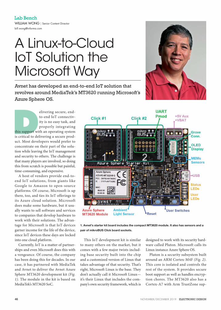
WILLIAM WONG | Senior Content Director
Avnet has developed an end-to-end IoT solution that revolves around MediaTek’s MT3620 running Microsoft’s Azure Sphere OS.
Lab Bench
Delivering secure, end-
to-end IoT connectiv-
ity is no easy task, and
properly integrating
this support with an operating system
is critical to delivering a secure prod-
uct. Most developers would prefer to
concentrate on their part of the solu-
tion while leaving the IoT management
and security to others. The challenge is
that many players are involved, so doing
this from scratch is possible but painful,
time-consuming, and expensive.
A host of vendors provide end-to-
end IoT solutions, from giants like
Google to Amazon to open-source
platforms. Of course, Microsoft is up
there, too, and ties its IoT offerings to
its Azure cloud solution. Microsoft
does make some hardware, but it usu-
ally wants to sell software and services
to companies that develop hardware to
work with their solutions. The advan-
tage for Microsoft is that IoT devices
garner income for the life of the device,
since IoT devices these days are locked
into one cloud platform.
Currently, IoT is a matter of partner-
ships and even Microsoft does this with
a vengeance. Of course, the company
has been doing this for decades. In our
case, it has partnered with MediaTek
and Avnet to deliver the Avnet Azure
Sphere MT3620 development kit (Fig.
1). The module in the kit is based on
MediaTek’s MT3620 SoC.
This IoT development kit is similar
to many others on the market, but it
comes with a few major twists includ-
ing base security built into the chip
and a customized version of Linux that
takes advantage of that security. That’s
right, Microsoft Linux is the base. They
don’t actually call it Microsoft Linux—
it’s their Linux that includes the com-
pany’s own security framework, which is
designed to work with its security hard-
ware called Pluton. Microsoft calls its
Linux instance Azure Sphere OS.
Pluton is a security subsystem built
around an ARM Cortex-M4F (Fig. 2).
This core is isolated and controls the
rest of the system. It provides secure
boot support as well as handles encryp-
tion chores. The MT3620 also has a
Cortex-A7 with Arm TrustZone sup-
A Linux-to-Cloud IoT Solution the Microsoft Way
1. Avnet’s starter kit board includes the compact MT3620 module. It also has sensors and a
pair of mikroBUS Click board sockets.
46 NOVEMBER/DECEMBER 2019 ELECTRONIC DESIGN

port for heavy lifting and running the
Azure Sphere OS. Another Cortex-M4F
handles most of the peripherals. There’s
also wireless support, including dual-
band Wi-Fi. That has its own dedicated
processor.
NXP Semiconductors announced an
i.MX 8 platform with Pluton support
that’s similar to MediaTek’s chip. NXP’s
chip will also run the Azure Sphere OS.
I like the design of the development
board. The MT3620 chip is actually
on a module (Fig. 3) that incorporates
the wireless support, which has FCC
approval. This makes using the module
a snap for developers, since additional
FCC approval of a product may not be
necessary. An on-module antenna and
a connector are included for a separate
antenna. The pinouts are nicely por-
tioned, making design of a carrier board
a snap.
The mikroBUS Click board sockets
are a handy way to add extra sensors to
augment the ones already on the board
(Fig. 4). These include an ambient light
sensor, three-axis accelerometer, three-
axis gyro, temperature sensor, and
barometric pressure sensor. There’s also
an unpopulated Pmod socket solder
pad, but it shares space with one of the
Click board sockets. A couple of I2C
sockets for displays and Grove inter-
faces are in the mix, too. Power sock-
ets can be soldered on, but power can
also be supplied by the USB interface
used for initial configuration as well as
debugging.
GETTING STARTED
Now that we’re done with the long
explanation about the hardware and
operating system, we can move onto
what it took to get started. The kit comes
in a small box with the board and a short
USB cable. The page of directions, typi-
cal these days, directs you to the web for
more details.
The board comes preprogrammed,
but there’s nothing to do with it until you
download a bunch of Microsoft soft-
ware on to your PC, including Micro-
2. The MT3620 block diagram highlights the Corex-M4F-based Pluton security subsystem.
The Cortex-A7 runs Microsoft’s Linux-based Azure Sphere OS.
3. The MediaTek MT3620 is available on Avnet’s module used in the development kit. The
pinouts are easy to work with when designing a custom PCB.
47GO TO ELECTRONICDESIGN.COM

IoT Solution
soft Visual Studio and the Azure SDK.
You also need a free account on Azure to
connect your newly acquired dev board
to the cloud.
I won’t bore you with the details
because there are quite a few. Likewise,
a number of blogs, PDF files and vid-
eos about this platform are available.
Unfortunately, though, there’s not one
place to find all of them. They’re also
all over the place from Avnet’s web-
site, to MediaTek to Microsoft and also
Element 14. This is where I found a
three-part blog entitled Avnet’s Azure
Sphere Starter-Kit (Out of Box Demo).
It duplicates information found in oth-
er sources, but it’s the best for getting
started.
The blog and other sources are need-
ed because this kit is designed to be used
for development, not just evaluation
of an IoT end-to-end solution. In that
sense, it’s an ideal platform for devel-
opers, since it’s designed to work with
the tools that include Azure Sphere and
Visual Studio.
The first blog post addresses initial
setup and configuration of the board.
The second gets into connecting to the
cloud and setting up a logical, cloud-
based IoT hub that’s used manage the
device; in this case, the dev board. The
result of this second blog is support for
Azure’s Time Series Insights (Fig. 5).
This is just one aspect of Azure Sphere.
The third blog gets into using IoT Cen-
tral. I still need to finish this one, but
I don’t get a lot of large blocks of free
time.
Though it will take a day or three
to get to this point, the results are well
worth the effort. Once completed, you
have the Visual Studio and SDK all set
up and have a couple projects in the bag
albeit canned demos from the walk-
through.
I still need to explore the develop-
ment side of things, especially the Azure
Sphere OS’s security aspects and how
they differ from support like SELinux
or Ubuntu’s AppArmor, which I’m more
familiar with. I won’t even mention the
Azure side of things, as cloud develop-
ment is a whole other area of develop-
ment.
In closing, I will mention that the kit
differs from many others in that it comes
locked down. It’s not an open system on
a network when you plug it in, and it
takes time and effort to get to the point
of doing the programming. This is actu-
ally a good thing, because it works from
the opposite approach of being very
open and unsecured. It would be nice if
other development platforms followed
this rule.
On the flip side, the system locks you
into hardware, a toolset, an operating
system, and cloud provider. But this
tends to be par for the course when it
comes to most IoT solutions. The big
hook to all the “free software” is monthly
charges for cloud support. Again, this
is the norm for an IoT solution where
you’re not providing your own cloud.
Though it’s taken me a while to get the
kit to do what I expected, I’m happy with
the results. I don’t claim to be an expert
at developing IoT apps for the MT3620,
but I have a good starting point.
4. A range of Click boards are available from a number of sources; it’s easy to design custom
boards given the limited number of interface pins.
5. Azure Sphere’s web-based cloud interface provides access to the data delivered from the
MT3620.
48 NOVEMBER/DECEMBER 2019 ELECTRONIC DESIGN

HIGH VOLTAGE MICROSIZE POWER SUPPLIES
OUTPUTS UP TO 1.5KV & 1 W
CUSTOM SOLUTIONS AVAILABLE
BIG PERFORMANCE
small size,
www.deantechnology.com
Contact DTI today to find out about the exact power supply
for your high voltage design.

AD5758 and ADP1031Complete System Solution for Industrial Analog Output Modules
X Enables eight channel-to-channel isolated outputs at under 2 W.
X Integrates critical features that reduce existing module footprints.
X 9HULoHG�UREXVW�(0,�(0&�PLQLPL]HV�GHVLJQ� time and adoption risk.
Buy Now at mou.sr/AD5758 and mou.sr/ADP1031