The Application of Palladium in E lectronic Connectors · The in E Application of Palladium...
12
The in E Application of Palladium lectronic Connectors CONTINUING STUDIES RESULT IN GROWING USE By Morton Antler Bell Telephone 1,aboratories. Inc.. Columbus, Ohio I’alladiurri and palladium- hnscd materials arc bring in( rcnsingh acccp.ptPd as substitutes for gold in contacts #or scpar(ibl(, idi,ctronic conrw tors. Sinw 107.5 the fm.ournhlc> rapt of pnllarliiirn rdtrtii (1 to gold has stiinulatcd rcscarrh in niuny arrws of coritnr I tc~chnologi. including manufacturing proccsscjs, contuc’t phcnomcvia, tcistirig and connector dmign. This has resulted in thc dci rdopmcvt of siwwl ncu materials wstcms involving c1cctrodqx)sitcd coatings. (kt inlays and wddmc~nts ofpalladium, palladruni -silccr nhs. gold-pollodiurri-cilz cr compositions and composite coatings u ith othvr mctuls thot ar (1 c7quivalmt to all-gold swtcms in many applications. This r(’i ~PW tracm thP histor, of rcwarch on palladiiim for usc in connwtors, urid sum- mariscas important results of studivs of the cntwonmwtul, tribological arid contnct propc’rtic’s of pnllnciium motorinls. Palladium and palladium alloys, such as 60palladium-40 silver and 73 palladium- 27 nickel, have a long history of use in contacts in the electronics industry. Their characteristics of erosion resistance, nobility, ease of fabrica- tion and moderate cost have made palladium materials the premier choice since 1950 for light duty open relay contacts in telecom- munications. The consumption of palladium worldwide for this application was in excess of a million troy ounces in 1974 (I). The need for relays in telephone apparatus is, however, rapidly declining because of the development of solid state switching systems that are smaller, consume less power, operate faster and are less expensive than comparable electromechanical equipment. Nevertheless, palladium will con- tinue to be used in significant amounts to service existing apparatus, at least until the year 2000, as well as in other relay applications. From about 1955 the use of printed circuit boards and separable electronic connectors has grown rapidly. Their combined annual produc- tion in the United States is valued at several billion dollars. World manufacture is estimated to be about three times greater. This has occurred because printed circuit boards are ideal structures for mounting and interconnect- ing components and integrated circuits, and separable connectors are needed to be able to join printed circuit boards as well as other building blocks of modern electronic systems. Connector functions can be viewed as occurr- ing at various levels of “pluggability”, from small to large in system complexity. For example, connectors attach components to printed circuit boards, boards to boards on a chassis, one chassis to another in the same cabinet, or one piece of equipment to another, usually via cables (2). Figure 1 illustrates several common types of separable electronic connectors. Corrosion resistance, high conductivity and mechanical durability are essential require- ments of a contact material. Ease of fabrication and availability are also necessary. Gold is the dominant metal for high reliability in long life separable electronic contacts, and recently Platinum Metals Rev., 1982, 26, (3), 106-117 106
Transcript of The Application of Palladium in E lectronic Connectors · The in E Application of Palladium...
The in E
Application of Palladium lectronic Connectors
CONTINUING STUDIES RESULT IN GROWING USE
By Morton Antler Bell Telephone 1,aboratories. Inc.. Columbus, Ohio
I’alladiurri and palladium- hnscd materials arc bring i n ( rcnsingh acccp.ptPd as substitutes for gold in contacts #or scpar(ibl(, idi,ctronic conrw tors. Sinw 107.5 the fm.ournhlc> rapt of pnllarliiirn rdtrtii (1 to
gold has stiinulatcd rcscarrh in niuny arrws of coritnr I tc~chnologi. including manufacturing proccsscjs, contuc’t phcnomcvia, tcistirig and connector dmign. This has resulted in thc dci rdopmcvt of s i w w l n c u materials wstcms involving c1cctrodqx)sitcd coatings. (kt inlays a n d w d d m c ~ n t s ofpal ladium, palladruni -silccr n h s . gold-pollodiurri-cilz cr compositions and composite coatings u ith othvr mctuls thot a r (1
c7quivalmt to all-gold swtcms in many applications. This r(’i ~ P W tracm thP histor, of rcwarch o n palladiiim for usc in connwtors, urid sum- mariscas important results of studivs of the cntwonmwtul , tribological arid contnct propc’rtic’s of pnllnciium motorinls.
Palladium and palladium alloys, such as 60palladium-40 silver and 73 palladium- 27 nickel, have a long history of use in contacts in the electronics industry. Their characteristics of erosion resistance, nobility, ease of fabrica- tion and moderate cost have made palladium materials the premier choice since 1950 for light duty open relay contacts in telecom- munications. The consumption of palladium worldwide for this application was in excess of a million troy ounces in 1974 (I). The need for relays in telephone apparatus is, however, rapidly declining because of the development of solid state switching systems that are smaller, consume less power, operate faster and are less expensive than comparable electromechanical equipment. Nevertheless, palladium will con- tinue to be used in significant amounts to service existing apparatus, at least until the year 2000, as well as in other relay applications.
From about 1955 the use of printed circuit boards and separable electronic connectors has grown rapidly. Their combined annual produc- tion in the United States is valued at several
billion dollars. World manufacture is estimated to be about three times greater. This has occurred because printed circuit boards are ideal structures for mounting and interconnect- ing components and integrated circuits, and separable connectors are needed to be able to join printed circuit boards as well as other building blocks of modern electronic systems.
Connector functions can be viewed as occurr- ing at various levels of “pluggability”, from small to large in system complexity. For example, connectors attach components to printed circuit boards, boards to boards on a chassis, one chassis to another in the same cabinet, or one piece of equipment to another, usually via cables ( 2 ) . Figure 1 illustrates several common types of separable electronic connectors.
Corrosion resistance, high conductivity and mechanical durability are essential require- ments of a contact material. Ease of fabrication and availability are also necessary. Gold is the dominant metal for high reliability in long life separable electronic contacts, and recently
Platinum Metals Rev., 1982, 26, (3), 106-117 106

Fig. 1 Various types of electronic connectors:
Top. ( a ) Dual-in-line semiconductor integrated circuit receptacle \riddle ( b ) Connectors for printed circuit boards with edge contacts
Bottom ( c ) Rectangular connector for chassis mounting
(a) Lourtvc) of the Rurnd) Cnrporatian (h)and(r)(vurtrk.efAMPIncnrporalpd
Platinum Metals Rev., 1982, 26, (3) 107
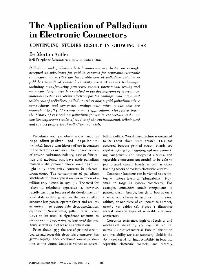
annual world consumption of gold for this purpose has been in excess of a million troy ounces. Its expense is a significant part of the costs of connectors and printed circuit boards, and from their earliest use there has been interest in lower cost alternative contact materials (3). It is obvious, therefore, that palladium would be a focus of attention as a replacement for gold in these products. However, the economic incentive to exploit palladium was not compelling until the decade of the 1970s when gold costs began to escalate, price trends are illustrated in Figure 2 .
Early Use of Palladium in Connector Contacts
The use of palladium was small in the 1960s, the main application being in a British Post Office prototype system when 3,000 to 4,000
troy ounces a year were used for contacts electroplated directly on the edges of printed circuit boards (4). Although it was recognised that palladium might have some technical disadvantages in being less noble than gold, a compensating factor was the better com- patibility of palladium plating solutions with board materials by comparison with common gold plating solutions of the time. Also, its resistance to sliding wear from contact engage- ment and separation was better than that of a gold electrodeposit against which it was com- pared (4). Experience with the system of gold alloy contact connectors mated to palladium edge plated boards was satisfactory (5).
During the 1960s studies of palladium electroplating processes and contact properties continued, and in 1972 a major connection system was committed to palladium (6). This consisted of wire contacts soldered in holes in printed circuit boards forming a pin field to which separable connectors with 75 gold- 25silver alloy contacts were joined. In this product palladium is electrodeposited on nickel wire pins, with the initial annual consumption of 10,000 to 20,000 troy ounces a year (7). As the price differential between palladium and gold continued to widen during the late 1970s to the present, interest in palladium heightened
and commercial connectors with palladium and palladium alloy contacts have begun to appear in the United States, Japan and West Germany, as well as in other countries. There is interest also in palladium as a gold replacement in switches for low energy applications, an example being a small multi-pole device that can be mounted on printed circuit boards (8). This device has 6opalladium-40 silver contacts that mate to gold plated members.
Fabrication of Palladium Connector Contacts
Palladium is used on connector contacts as weldments, electrodeposits or claddings. Weld- ments are made by fusing palladium wire to a copper alloy contact spring, clipping the wire, and then coining to the desired shape, usually a dome. Metal thickness usually ranges from 25 to 75,um. Most palladium is currently used as the electrodeposit at thicknesses from 0.5 to 2.5 pm on nickel underplate. Processes that plate the metal selectively on the functional
Platinum Metals Rev., 1982, 26, (3) 108
surfaces are widely used to reduce costs. Clay inlay palladium and palladium alloys
are becoming increasingly important because their placement on a contact structure is inherently selective and because novel alloys, unobtainable by electrodeposition and having especially desirable contact properties, can be obtained. Typical inlay thicknesses range from I to 5 ,urn. Little palladium is presently used for the edge contacts of printed circuit boards. The following discussion considers electroplated and clad coatings in detail.
Electrodeposited Palladium There are several considerations in palladium
deposition in common with all plating processes; the solutions should: [i] be easy to control, [ii] be usable at a wide range of operat- ing conditions (including temperature, agitation and cathode current densities), and have good throwing power, [iii] not be easily poisoned by impurities, and be able to plate on common sub- strates without attacking them or depositing spontaneously prior to the application of current, [iv] be capable of operating at both the high speeds of modern plating equipment used for gold at current densities of T O to 5 0 A/dm2, as well as the modest plating rates of con- ventional barrel and rack equipment, and [v] give smooth crack-free adherent coatings.
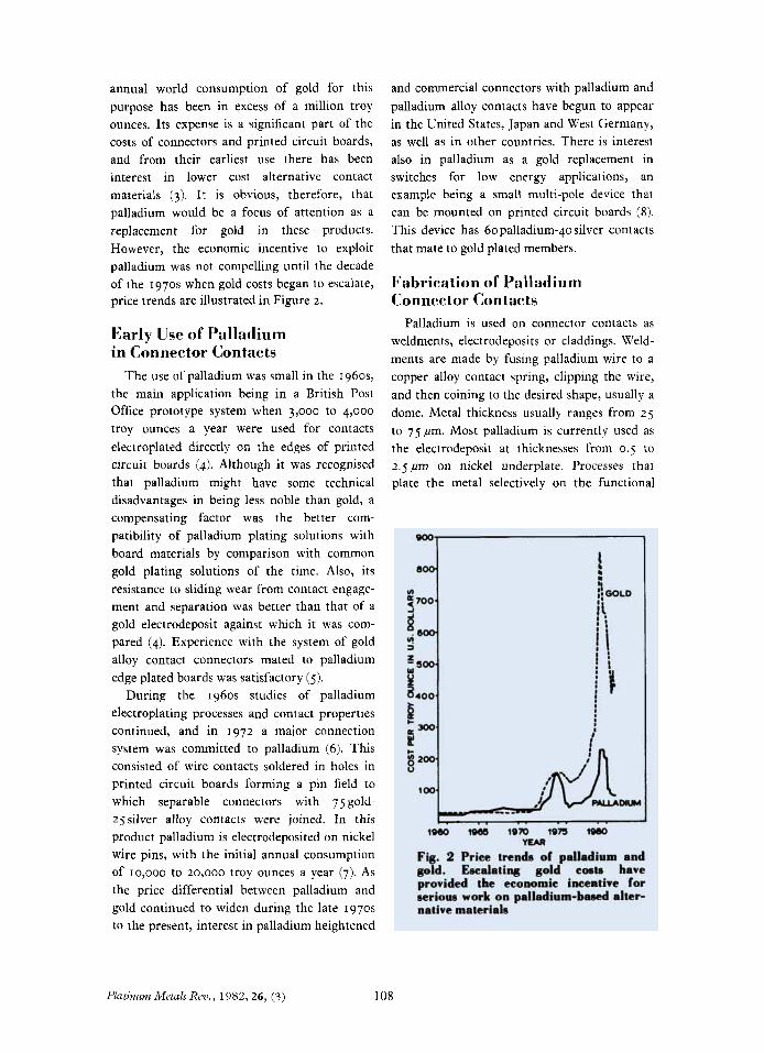
Many palladium plating processes evolve hydrogen at the workpiece which is readily absorbed by the deposit. The absorption limit is 67 atom per cent at one atmosphere and 20°C, while the solubility limit of a-palladium is 3 atom per cent hydrogen. At higher concentra- tions, P-PdH forms, this having the same face centred cubic structure as a-I’d, but with a 4 per cent larger lattice constant. Furthermore, P-PdH spontaneously loses hydrogen at room temperature, causing severe internal stress in the deposit which is relieved by crack formation (9). Figure 3 shows a slightly cracked deposit obtained from a commercial palladium plating process. Such deposits may be porous to the substrate and can, of course, have inferior mechanical characteristics.
Important palladium electroplating processes
Platinum Metals Rev., 1982, 26, (3) 109
Fie. 3 Palladium electrodeposit (2.5 ,unr thick). (:racks wrre caused by the spontaneous convwsion of D-l’dH LO ru-Pd with 1osq of hydrogen and shrinking of the drposil
include: [a] ammoniacal systems in which the palladium is complexed in diammino or tetra- ammino forms (91, such as Pd(NH,),(NO,), (p-salt), and Pd(NH,),CI,, [b] slightly acid systems containing chelated palladium (TO),
and [c] strongly acidic electrolytes like one con- taining palladium nitrate, palladium sulphite, and sulphuric acid (9). The latter system co- deposits from o . ~ to 10 per cent sulphur depending upon operating conditions, and the plating is said to contain very little hydrogen. Palladium electrodeposition processes with improved operating characteristics are, how- ever, rapidly being developed. Recent studies have described the pulse plating of palladium (I I, IZ), while deposit structures, mechanical characteristics and contact behaviours of pal- ladium electrodeposits are also being studied, although little critical information has thus far appeared in the technical literature. Until now no process for electroplating palladium has emerged which is clearly superior for electric contacts, most of the cited systems being deficient in some respect when considered from the process requirements for electroplating listed earlier. In t h s respect, the development of palladium plating for contact applications is in about the same status as gold twenty years ago.
Special mention should be made of palladium alloy electrodeposits. Palladium-nickel platings, xPd( ~oo-x)Ni, where x typically ranges from 50

to 80 per cent, are available ( I 3). While cheaper than pure palladium, such deposits can be expected to be less noble, although undoubtedly suitable for some applications. Processes that yield gold-palladium ( I 4) and palladium-silver (I 5 ) have been described, the latter electrodeposit being of great interest because of the good contact properties of palladium-silver alloys, described later; however, the bath that was developed is extremely corrosive and requires gold undercoats to protect the base metal substrates from the plating solution.
Clad Palladium Initial development of clad inlay processes
for electronic connector contacts occurred in the early 1960s. Their acceptance in the United States was slow at first because inlays require that connectors be designed specifically for them, involving stamping from sheet metal followed by forming to the finished shape with the inlay located in the contact position. Manufacturing processes involving screw machining of wire to form pins and sockets were entrenched, gold electroplating technology was well developed, the economic incentive to conserve noble metal was less than it is now, and finally there was general reluctance to locate noble metals selectively on contact
assemblies because of concern that base metal corrosion might occur in use which could result in contamination of the contact surface. The development of large scale applications for clad inlay contacts came first in Europe.
The clad inlay process is illustrated in Figure 4. Precious metal strip, usually a bimetallic layer of thin noble metal on thick nickel, called an interliner, is placed in a groove produced by skiving the substrate. The composite is then compressed at high pressure between rolls; a metallurgical bond forms due to extension of the rolled material which creates fresh surface at the layer interface. Several heat treatment and rolling stages may be necessary to obtain the desired reduction and substrate temper. Surface contamination, including transfer of base metal from the substrate to the rolls from which it can back transfer to the noble metal in subsequent production, is minimised by lubrica- tion of the workpiece and dressing of the rolls.
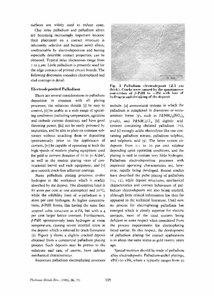
Electroplated metals cannot generally with- stand forming because they are relatively brittle and tend to crack. B’rought ductile metals, however, lend themselves to this purpose. Pure gold and gold-silver alloys, for example 70 gold- 30 silver, have been extensively used in inlays, and this practice has been extended to palladium and palladium-silver, from 60 palladium-40 silver to 30 palladium-70 silver (16). Figure 5 shows stamped formed contacts made from clad inlay palladium. As discussed later, 6opalladium-40 silver is a unique contact material, more noble that pure palladium, as well as being considerably cheaper, see Table. The non-availability of a practical electroplat- ing process for making palladium-silver alloys is an added incentive to use clad materials. Gold- palladium-silver alloys, such as 39Au3oPd(3 I-
x)Ag(xSn,In) ( I 7) that combine high nobility with good formability, have rccently been developed.
A disadvantage of claddings is that it is difficult to make them as thin as electrodeposits without their becoming highly porous. This is because slight roughening at the two interfaces, substrate to interliner and interliner to noble metal, occurs during rolling and can lead to
Platinum Metals Rev., 1982, 26, (3) 110
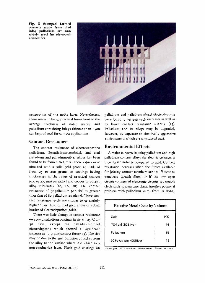
Fig. 5 Stamped formrd contarts made from clad inlay palladium arr now w i d d y used for elrctronic connectors
Gold
70Gold-30Silver
Palladium
60 Palladium-40Silver
penetration of the noble layer. Nevertheless, there seems to be no practical lower limit to the average thickness of noble metal, and palladium-containing inlays thinner than I pm can be produced for contact applications.
Contact Resistance The contact resistance of electrodeposited
palladium, 80 palladium-20 nickel, and clad palladium and palladium-silver alloys has been found to be from I to 3 ml2. These values were obtained with a solid gold probe at loads of from 25 to 200 grams on coatings having thicknesses in the range of practical interest (0.5 to 2.5 ,urn) on nickel and copper or copper alloy substrates (10, 16, 18). The contact resistance of 50 palladium-so nickel is greater than that of So palladium-20 nickel. These con- tact resistance levels are similar to or slightly higher than those of clad gold alloys or cobalt hardened electrodeposited golds.
There was little change in contact resistance on ageing palladium coatings in air at iz5OC for 30 days, except for palladium-nickel eiectrodeposits which showed a significant increase at 10 grams contact force (13). The rise may be due to thermal diffusion of nickel from the alloy to the surface where it oxidised to a non-conductive layer. Flash gold coatings on
100
64
19
12
pqlladium and palladium-nickel electrodeposits were found to mitigate such increases as well as to lower contact resistance slightly ( I 3). Palladium and its alloys may be degraded, however, by exposure to chemically aggressive environments which are considered next.
Environmental Effects A major concern in using palladium and high
palladium content alloys for electric contacts is their lesser nobility compared to gold. Contact resistance increases when the forces available for joining contact members are insufficient to penetrate tarnish films, or if the low open circuit voltages of electronic circuits are unable electrically to puncture them. Another potential problem with palladium stems from its ability
Relative Metal Costs by Volume
Platinum Metals Rev., 1982, 26, (3) 111
Where:gold::$500,palladium-$150 and silver..$25 per troy
ounce
to catalyse the formation of tough insulating organic surface layers which originate from traces of organic air pollutants. Considerable research has been conducted recently on both the corrosion and polymerisation problems.
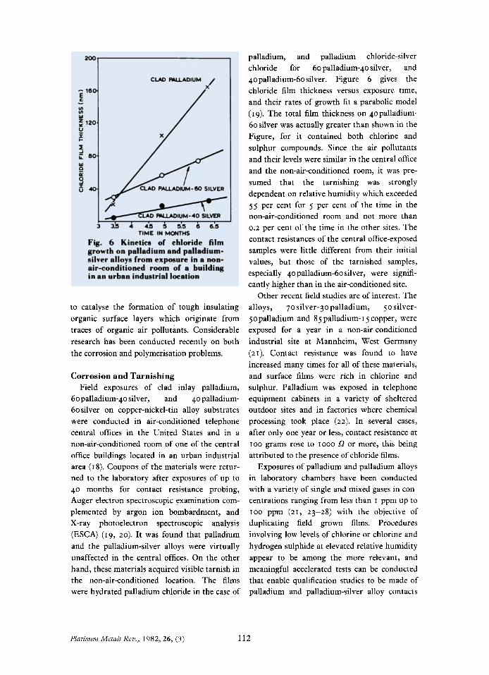
Corrosion and Tarnishing Field exposures of clad inlay palladium,
6opalladium-40 silver, and 40 palladium- 60 silver on copper-nickel-tin alloy substrates were conducted in air-conditioned telephone central offices in the United States and in a non-air-conditioned room of one of the central office buildings located in an urban industrial area ( I 8). Coupons of the materials were retur- ned to the laboratory after exposures of up to 40 months for contact resistance probing, Auger electron spectroscopic examination com- plemented by argon ion bombardment, and X-ray photoelectron spectroscopic analysis (ESCA) (19, 20). It was found that palladium and the palladium-silver alloys were virtually unaffected in the central offices. On the other hand, these materials acquired visible tarnish in the non-airxonditioned location. The films were hydrated palladium chloride in the case of
palladium, and palladium chloride-silver chloride for 60 palladium-40 silver, and 4opalladium-60 silver. Figure 6 gives the chloride film thickness versus exposure time, and their rates of growth fit a parabolic model (19). The total film thickness on 4opalladium- 60 silver was actually greater than shown in the Figure, for it contained both chlorine and sulphur compounds. Since the air pollutants and their levels were similar in the central office and the non-air-conditioned room, it was pre- sumed that the tarnishing was strongly dependent on relative humidity which exceeded 55 per cent for 5 per cent of the time in the non-air-conditioned room and not more than 0.2 per cent of the time in the other sites. The contact resistances of the central office-exposed samples were little different from their initial values, but those of the tarnished samples, especially 40 palladium-60 silver, were signifi- cantly higher than in the air-conditioned site.
Other recent field studies are of interest. The alloys, 70 silver-30 palladium, 5 0 silver- sopalladium and 85palladium-15 copper, were exposed for a year in a non-air-conditioned industrial site at Mannheim, West Germany (21). Contact resistance was found to have increased many times for all of these materials, and surface films were rich in chlorine and sulphur. Palladium was exposed in telephone equipment cabinets in a variety of sheltered outdoor sites and in factories where chemical processing took place (22). In several cases, after only one year or less, contact resistance at I 00 grams rose to I ooo f2 or more, this being attributed to the presence of chloride films.
Exposures of palladium and palladium alloys in laboratory chambers have been conducted with a variety of single and mixed gases in con- centrations rangmg from less than I ppm up to roo ppm (21, 23-28) with the objective of duplicating field grown films. Procedures involving low levels of chlorine or chlorine and hydrogen sulphide at elevated relative humidity appear to be among the more relevant, and meaningful accelerated tests can be conducted that enable qualification studies to be made of palladium and palladium-silver alloy contacts
Platinum Metals Rev., 1982, 26, (3) 112
(28). An evaluation of clad 39Au3oPd(31- x)Ag(xSn,In) in a mixed gas test showed it to be comparable to the widely used high gold alloy, 7ogold-josilver (17). An interesting study of creep of tarnish films from a copper alloy over the surfaces of gold and palladium with which it was in contact has recently been made (29). This configuration can occur with selectively coated materials such as inlays. In a hydrogen sulphide atmosphere at 50 per cent relative humidity, sulphide creep was significantly greater over gold than over palladium.
To summarise, palladium appears to be stable in many environments provided relative humidity does not exceed 55 per cent. The 6opalladium-40 silver alloy is more noble than palladium, and alloys having 60 per cent or greater silver contents are less noble than palladium. Gold-palladium-silver alloys con- stitute another class of wrought metals having low reactivity. Sulphur compounds, such as hydrogen sulphide, and parts per billion levels of certain gaseous chlorine compounds, may react with palladium and many of its alloys. Although pure gold is little affected by these environments, creep of tarnish films from adjacent base metals onto palladium may be less extensive than onto gold. Porous palladium would appear similarly to have an advantage over porous gold.
Reactivity of Pal lad ium with Organic Air Pol lutants
Palladium, platinum and rhodium when exposed to room air have been found to acquire fragile films which were determined to be hydrocarbons by pyrolysis gas chromatographic analysis (30). After about one year films on the palladium were 10 nm thick, and using a gold probe a force of 270 grams was required to penetrate the film on polished palladium and to establish substantial metallic contact, defined as a contact resistance below 10 m.0. These observations are in agreement with earlier work in which palladium was exposed at room temperature to organic vapours (3 I) . In com- parable conditions gold does not produce such films. It is believed that the platinum group
metals catalyse polymerisation of adsorbed organic air pollutants to produce these insulat- ing layers. The term “static polymer” refers to such films, which differentiates them from “frictional polymers” that are discussed later.
There is some conjecture concerning the practical significance of static polymers on con- nector contacts. According to one investigator (32), it is possible that plastic materials com- monly used in the construction of connector housings and other electronic components may produce volatiles above IOOT which can sig- nificantly increase the contact resistance of electrodeposited palladium in their vicinity due to polymer formation. A flash of gold plate on palladium was found to reduce this tendency.
Tribological Properties It is essential that contacts be wear resistant,
since separable electronic connectors may be mated and disengaged many times. Badly disrupted coatings in which base metal sub- strates and underplates are exposed generally result in high contact resistance, particularly in aggressive environments. It is desirable also that sliding friction be low so as to allow large numbers of contacts to be designed into a con- nector. Tribology refers to the friction and wear of mated contacts during sliding, and included in this field of study is wear due to fretting which originates in differential expansions of the contact members due to fluctuating ambient temperature, external vibrations, and other causes. Motions of the order of tens of pm may occur which can lead to the formation of insulating frictional polymers on palladium and other catalytically active metals, and to the accumulation of oxidised wear debris in the contact zone once the noble metal coating has worn through.
Sl iding W e a r The basic mechanisms of the wear and
lubrication of metallic contacts have been extensively reviewed by the author (33-37). It is appropriate, however, to identify those aspects of wear that are especially relevani to palladium. Pure wrought palladium-like gold,
Platinum Metals Rev., 1982, 26, (3) 113
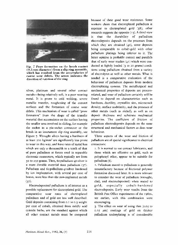
Fig. 7 Prow formation on the brush rontart ( 0 . 5 mm diameter) from a slip ring assembly, which ha6 resulted from the accumulation of coarse wear dehris. The ar row indicates Ihe dirertion of rotation of thr ring
silver, platinum and several other contact metals-being relatively soft, is a poor wearing metal. It is prone to cold welding, severe metallic transfer, roughening of the contact surfaces and the formation of coarse wear debris. This mechanism of wear is called “prow formation” from the shape of the transfer material that accumulates on the surface having the smaller area involved in sliding, for example the socket in a pin-socket connector or the brush in an instrument slip ring assembly, see Figure 7. Wrought alloys having a hardness of at least 200 kdmm2 are significantly less prone to wear in this way, and have rates of metal loss which are only a thousandth to a tenth of that of pure palladium at forces used in separable electronic connectors, which typically are from 50 to 250 grams. Thus, 6opalladium-4o silver is a more durable material than palladium (37). Palladium and 60 palladium-40 silver hardened by ion implantation, with several per cent of boron, wore less than the non-implanted metals
Electrodeposited palladium is of interest as a possible replacement for electroplated gold. The comparative wear rates of electroplated palladium and of gold are less well described. Gold deposits containing from 0.1 to 0.3 weight per cent of cobalt, obtained from mildly acid cyanide baths, are the standard against which all other contact metals must be compared
(37).
because of their good wear resistance. Some workers claim that electroplated palladium is superior to electroplated gold (38); other research suggests the opposite ( I 3). A third view is that the durability of palladium electrodeposits depends on the processes from which they are obtained (40), some deposits being comparable to cobalt-gold with other palladium platings being inferior to it. The latter opinion is probably correct and parallels that of early wear studies (41) which were con- ducted at lightly loaded (3 to 20 grams) condi- tions using palladium obtained from a variety of electrolytes as well as other metals. What is needed is a comparative evaluation of the behaviour of palladium deposits from modern electroplating systems. The metallurgical and mechanical properties of deposits are process- related, and wear of palladium certainly will be found to depend on characteristics such as hardness, ductility, crystallite size, microcrack density, surface nodularity, and the presence of other metals (such as nickel), as well as on deposit thickness and substrate mechanical properties. The coefficient of friction of palladium electrodeposits depends on the same structural and mechanical factors as does wear behaviour.
Three aspects of the wear and friction of palladium are of special significance to electrical connectors:
I. It is normal to use contact lubricants, and those which are effective on gold, such as polyphenyl ether, appear to be suitable for palladium (6). 2. Palladium mated to palladium is generally unsatisfactory because of frictional polymer formation discussed later. It is more relevant to consider the wear of palladium (wrought, clad, and electrodeposited) when mated to g o l d , e s p e c i a l l y c o b a l t - h a r d e n e d electrodeposits. Early wear results from the British Post Office experiments of the 196os, see earlier, with this combination were encouraging. 3. The effect on wear of using thin (0.05 to 0.25 pm) coatings of gold on thicker palladium underplating is of considerable
Platinum Metals Rev., 1982, 26, (3) 114
interest. Such coatings reduce the rate of wear of palladium and have a salutory effect on its tarnishing (39,42).
Fretting and Friction Yolymerisatian The catalytic properties of freely exposed
palladium can lead to the formation of electrically insulating static polymers. When palladium is mated to palladium and fretting occurs, the rate of frictional polymer formation is much greater than in the static case and high contact resistance often develops (43). It has been postulated that wiping creates fresh sur- faces that enhance polymer development and, because fretting displacements are small, there is little chance that contact surfaces will be scrubbed clean.
Practical experience with all-palladium con- tacts has generally shown them to be poor, but palladium mated to gold appears to solve the frictional polymer problem (8, 44). This is attributable to a tendency for gold to transfer to palladium, which makes the contact system effectively all-gold. This finding also reflects early experience with palladium in relay con- tacts (43) where the practice of using clad palladium against 22 carat gold-silver, on a palladium substrate, was found necessary to circumvent contact resistance difficulties due to frictional polymer. Alloying palladium with large amounts of non-polymer-forming metals can reduce the polymer problems to manage- able proportions; this is technologically import- ant with many palladium-silver, gold-palladium, and gold-palladium-silver systems (45).
It is important also that contact metals be durable. Thus, the thin palladium and gold- palladium composite coatings of current interest must have low fretting wear rates so as to avoid exposure of base substrate metal. If wear*ut occurs, oxide accumulation due to fretting corrosion also can cause unacceptably high contact resistance (46). The number of fretting cycles required to achieve a given rise in contact resistance due to frictional polymers increases with increasing force, and is inversely related to wipe distance (47).
Recent work has shown that contact
lubricants promote frictional polymerisation (47). Surprisingly, however, contact resistance is much less likely to rise because adhesion of polymers to the contact surface, a necessary requirement for polymer to accumulate, is retarded when lubricants are present. It is possible also that frictional polymers from some organic lubricants are structurally different from those that originate from adsorbed air pollutants on unlubricated surfaces.
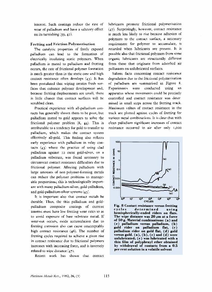
Salient facts concerning contact resistance degradation due to the frictional polymerisation of palladium are summarised in Figure 8. Experiments were conducted using an apparatus whose movements could be precisely controlled and contact resistance was deter- mined in small steps across the fretting track. Maximum values of contact resistance in the track are plotted against cycles of fretting for various metal combinations. It is clear that with clean palladium significant increases of contact resistance occurred in air after only 1,000
Platinum Metals Rev., 1982, 26, (3) 115

cycles of fretting on a 20 ,um track. Palladium versus gold is comparable to an all-gold system. Coating with a thin film of a fluid contact lubricant significantly lowered the tendency for contact resistance to rise.
Solderability In many cases it is necessary to join contact
members using tin-lead solders, and solid palladium and palladium electroplates on copper and copper alloys can be easily soldered (48). However, storage of palladium in damp environments prior to soldering may cause poor wetting when non-activated rosin fluxes are used; midly activated fluxes enhance wetting in such cases. Dissolution of palladium in solder is slower than in gold, but with I weight per cent and greater levels of palladium in 60 tin-40 lead solder, brittle joints are obtained. Another
study ( I 3) showed the quality of solder joints to rank in the order: gold (best), palladium and palladium-nickel alloy.
Conclusions T h e contact industry has long been
interested in palladium as a substitute for gold on separable electronic connectors, but only recently has the ratio of the costs of palladium to gold been sufficiently attractive to stimulate serious work on palladium-based materials. New manufacturing processes, novel palladium alloys and composite contact finishes have been developed which are in many applications equivalent i n performance to all-gold systems, while being considerably less expensive. Acceptance of palladium-based contacts is growing, and is a trend that is likely to continue in the foreseeable future.
References
I “Annual Review and Outlook”, 1978, J. Aron Commodities Corporation, New York
2 M. Antler, “Kirk-Othmer Encyclopedia of Chemical Technology”, Vol. 8, 3rd Edn., Wiley- Interscience, New York, p. 641
3 M. Antler, IEEE Trans. PHP, 1975, 11, 216 4 F. H. Reid, Plating, 1965, 51, 531 5 P. Preston, British Post Office, private
communication 6 D. T. Napp, I’roc. Fifth Plating in the Electronic
Ind. Symp., Am. Electroplaters’ SOC., New York, ‘975, P. 28
7 J. G. Donaldson, Plating, 1974,61, 222
8 W. R. Hain, J. A. Clisura and L. W. Rudloff, Proc. Holm Conf. on Electrical Contacts, Chicago, 1981, p. 241
9 C. J. Raub, Proc. Symp. on Economic IJse of and Substitution for Precious Metals in the Electronics Ind., Am. Electroplaters’ SOC., Danvers, Mass., 1980
10 R. J. Morrissey, Plating S u f . Finish., 1980, 67,
11 J.-M. Locarnini and N. Ibl, Proc. Second Int. Pulse Plating. Symp., Am. Electroplaters’ SOC., Roscmont, Ill., Oct. 1981
(12),44
I 2 N. Ibl, op. cit. 13 M. J. PikeBiegunski and R. Razzone, Proc.
Symp. on Economic Use of and Substitution for Precious Metals in the Electronics Ind., Am. Electroplaters’ Soc., Danvers, Mass., 1980
14 Anon., Plating Surf. Finish., 1980, 67, ( I I) , 36 15 c‘. Cohen, K. R. Walton and R. Sard, Abstr. 309,
Electrochem. SOC. Meeting, Denver, Oct. I 98 I
16 R. J. Russell and R. 0. Capp., Insul.lCircuiis, Mar. 1981, p. 34
17 A. Bischoff, R. Schnabl and F. A. Aldinger, Proc. Holm Conf. on Electrical Contacts, Chicago,
18 M. Antler, M. H. Drozdowicz and C. A. Haque, IEEE Truns. Components, Hybrids Munuf. Technol., 1981, CHMT-4, (4), 482
19 C. A. Haque and M. Antler, Proc. Holm Conf. on Electrical Contacts, Chicago, 1981, p. I 83
20 S. P. Sharma, op. cii., p. 191 21 L. Borchert, C. Mayer, A. Murr, J. Potinecke,
and K. L. Schiff, Proc. Ninth Int. Conf. on Electric Contact Phenom., Chicago, 1978, p. 273
22 M. Antler, Proc. Eleventh Int. Conf. on Electric Contact Phenom., West Berlin, June 1982
23 S. Shimosato, Electron. Commun. Jpn., 1972,
24 W. H. Abbott, Proc. Holm Seminar on Electrical Contacts, Chicago, 1973, p. 94
25 1:. R. Long and K . F. Bradford, Proc. Holm Conf. on Electrical Contacts, Chicago, 1975, p. 745
26 M. Antler and J. J. Dunbar, op. cit., ref. 18, 1978, CHMT-I, 17
27 L. Borchert and M. Murr, Proc. Tenth Int. Conf. on Electric Contact Phenom., Vol. 11, Budapest,
28 S. P. Sharma and E. S. Sproles, Proc. Holm Conf. on Electrical Contacts, 1981, p. 203
29 I<. R. Conrad, Proc. Annu. Connectors and Interconnections Symp., Philadelphia, Nov.
1981, P. 89
55-c, (9), 98
1980, P. 989
1981, P. 342
Platinum Metals Rev., 1982, 26, (3) 116

30 A. Fairweather, F. Lazenby and D. Marr, Trans.
31 S. W. Chaikin,EZectro-Technol., 1961,68,70 32 M. Huck, Proc. Ninth Int. Conf. on Electric
Contact Phenom., Chicago, 1978, p. 619 33 M. Antler, Platinum Metals Rev., 1966, 10, (I), 2
34 M. Antler, IEEE Trans. PHP, 1973, 9 ,4 35 M. Antler, up. cif., ref. 18, 1981, CHMT-4, (I),
1s 36 M. Antler, “Fretting of Electrical Contacts”,
Symp. on Mater. Eval. Under Fretting Condi- tions, Natl. Bur. Stand., Gaithersburg, Md., 3 June I 98 r , (ASI’M Spec. Tech. Publ. No. 780)
37 M. Antler, C. M. Preece and E. N. Kaufmann, op. cif., ref. 18, 1982, CHMT-5, (I), 8 1
38 H. Grossman, Trans. Imf. Met. Finish., 1978, 56, 54
39 T. Sato, Y. Matsui, M. Okada, K. Murakawa, and 2. Henmi, op. cit., ref. 18, 1981, CHMT-4, (I), 10
Inst. Met. Finish, 1976,54, 145 40
47 42
43
44
45
46
47
48
J. N. Crosby, Proc. Symp. on Economic IJse of and Substitution for Precious Metals in the Electronics Ind., Am. Electroplaters’ SOC., Danvers, Mass., r.980 H. C. Angus, Instrum. Prac., 1966, 20, 241 H. Grossmann and M. Huck, Proc. Tenth Int. Conf. on Electric Contact Phenom., Vol. 1, Budapest, I 980, p. 401 H. W, Hermance and 1‘. F. Egan, Bell Syst. Tech.
E. S. Sproles, Proc. Annu. Connectors and Interconnections Symp., Philadelphia, Nov., 1 9 8 1 , ~ . 267 W’. A. Crossland and l’. M. K . Murphy, IEEE Trans. PHI‘, 1974, 10, (I), 64 M. Antler, Proc. Electronic Components Conf., San Diego, Cal., May 1982 M. Antler and E. S. Sproles, op. cit., ref. 18, 1982,CHMT-5,(1), 158 R. G. Rader, op. cit., rrf. 40
39 ‘ 9 5 8 , 3 7 , 739
A New Platinum-Wired Air Flow Meter FUEL ECONOMY OF PETROL INJECTION ENGINES IMPROVED
‘The possibility of determining the velocity of air by measuring the electric current required to keep a resistance wire at a given temperature was suggested early this century by A. E. Kennelly and his colleagues, and was soon developed independently by a number of investigators. In I 9 14 work by Professor I,. \:. King of McGill University on the convection of heat from small cylinders in a stream of fluid was reported to the Koyal Society (Philos. Trans. R . Sac., London, Series A, 1914, 2x4, 373). His experiments had been undertaken to study the laws of convection of heat from thin platinum wires heated by an electric current, in order that the results could be used in the design of an anemometer capable of accurately measuring wind velocity. However his linear anemometer was considered to be useful for a number of applications including studies of tur- bulent flow and of air velocities in the neighbourhood of aeroplane surfaces and revolving blades, and for the measurement of temperatures and velocities of heated gases, or of flames.
Since that time the principle involved has been applied to an increasing number of‘ uses. Now a hot wire air mass meter is being developed by Robert Bosch GmbH of Stuttgart, \ h c t Germany to measure the mass of air drawn into automobile petrol injection engines and thus, with appropriate systems, to optimise the air to fuel ratio and hence fuel economy
-*,,
while limiting exhaust emissions (K. Sauer, S.A.E. Technical Paper 800468).
In the new meter a 70 micron diameter platinum wire forms part of a Wheatstone bridge circuit where the output voltage is held steady by regulating the heating current. Any increase in air flow cools the wire and causes a resistance drop. ’l’his is corrected within milliseconds as a controlled increase in the heating current signals the mass flow rate of the air and brings the platinum wire back to its former temperature. ‘1.0 allow for changes in the temperature of the intake air a temperature compensating resistor is located in the air stream. This has to be stable, corrosion-proof and fast responding, therefore a platinum film resistor is employed.
A disadvantage of the hot wire anemometer has always been the effects of dirt building up on the wire. Now the quality of the platinum employed enables this problem to be overcome by a process,that burns off the organic matter, and removes any inorganic particles embedded in it. This involves heating the platinum anemometer wire to a temperature of 800 to IOOOT for one or two seconds immediately after the engine has been stopped. A most important contribution to the overall perform- ance is the quality control of the platinum wire by automatic and continuous monitoring of mechanical integrity, electrical resistance and its temperature coefficient. T h e process is now being optimised by vehicle testing.
Platinum Metals Rev., 1982, 26, (3) 117