
TECHNOLOGY FOR OPTICAL CO-PACKAGING
6
TECHNOLOGY FOR OPTICAL CO-PACKAGING Yoichi Taira, Ph.D. Keio University Yokohama, Kanagawa, Japan [email protected] ABSTRACT Recent advancement of information and communication technology requires high-bandwidth data transmission. Signal transmission using optical fibers is widely used because of its extremely large signal bandwidth and length product. Since the signals in VLSIs are electrical, there is always a need for EO/OE converters in a form of optical transceiver/receiver. As the required I/O bandwidth to/from VLSIs such as switch chips and CPUs increases, conventional VLSI packaging faces the I/O bandwidth bottleneck. Optical co-packaging or optical transceivers on the package is the solution, where high bandwidth data I/O is carried out without using the bottom I/O channels of the package module. Although early examples of optical co- packaging relied on a package-on-package approach where packaged optical transceivers are socket mounted on a VLSI package, the whole package needs to be re-evaluated to support the volume demand to enable wide use of optical co- packaging such as for large-scale data-centers and 5G network. The assembly process and the long-term reliability of the components are some of the key matrices. The technology options will be discussed to realize optical co- packaging in terms of design materials and processing. Key words: optical interconnect, co-packaged optics, optical integration, optical co-packaging. INTRODUCTION Servers in data centers are getting more connected as the cloud workload moves more sophisticated use including big data analysis, deep learning, and large-scale modeling. High-bandwidth low latency link between the processors are the key for the high-performance computer (HPC) where the characteristics of the inter-processor data communication determine the performance of the HPC system. Optical fiber communication has been used for long haul data communication because of its large bandwidth-length product, or its ability of high bandwidth signal transmission over long distance without significant signal attenuation and irrecoverable distortion. Historically the use point-to-point optical fiber communication has been spreading from the long-distance communication including cross continent and trans-ocean communication, metro and campus communication to shorter distance communication of servers in data centers. As the data rate increases optical communication even inside the server rack is getting more common. NETWORK IN DATA CENTER Nowadays, data communication between server racks in the data centers are being done exclusively through optical fibers. Each server node in the data centers is usually connected to the external internet in some way. Initially, the server nodes are connected using a tree-like network. In this network, each node is at the leaf of the tree and a switch is placed where the trunk line branches. Since the network traffic getting larger as the line is near to the bottom, where the traffic is the largest, this network structure is called fat-tree. When each server node just runs an application of external user and the information traffic for the application is just between the node and the external user, this network structure works fine to satisfy the user’s demand. Figure 1 shows the typical data center network using fat-tree configuration. The use of the server in the data centers is expanding from a web service to more sophisticated data analysis such as deep learning and large-scale modeling. In the latter case, there are significant amount of inter node communication because the system works as a multi-processor system for these kinds of workload. The multi-hop switch network structure shown in figure 1 is not an ideal network structure because it takes a long time for the data packet from the origin node to reach the destination and this slows the application speed. This latency problem is eased by employing fabric-type network where any pair of the nodes can communicate only one or very small number of hops of the switch, where the communication latency is minimized. For this fabric type network, however, requires a large packet switch device, which has many connection high speed ports ToR Tier 1 Tier 1 Server Server Server Server Server Server Tier 2 Tier 2 Edge Spine Core Core Router DCI 10G SFP+ AOC Server Server Server Server Server Server Server Server Server Server Server Server 40G QSFP+ SR4 100G QSFP28 CWDM4 100G QSFP28 CWDM4 Server Server Server Server Server Server Tier 1 Tier 1 Access switches Aggregation switches WAN/Core router Core switches <100 m < 2 km < 2 km Figure 1. Fat tree data center network structure Proceedings of the SMTA Pan Pacific Microelectronics Symposium 2020 As originally published in the SMTA Proceedings
Transcript of TECHNOLOGY FOR OPTICAL CO-PACKAGING

TECHNOLOGY FOR OPTICAL CO-PACKAGING
Yoichi Taira, Ph.D. Keio University
Yokohama, Kanagawa, Japan [email protected]
ABSTRACT Recent advancement of information and communication technology requires high-bandwidth data transmission. Signal transmission using optical fibers is widely used because of its extremely large signal bandwidth and length product. Since the signals in VLSIs are electrical, there is always a need for EO/OE converters in a form of optical transceiver/receiver. As the required I/O bandwidth to/from VLSIs such as switch chips and CPUs increases, conventional VLSI packaging faces the I/O bandwidth bottleneck. Optical co-packaging or optical transceivers on the package is the solution, where high bandwidth data I/O is carried out without using the bottom I/O channels of the package module. Although early examples of optical co-packaging relied on a package-on-package approach where packaged optical transceivers are socket mounted on a VLSI package, the whole package needs to be re-evaluated to support the volume demand to enable wide use of optical co-packaging such as for large-scale data-centers and 5G network. The assembly process and the long-term reliability of the components are some of the key matrices. The technology options will be discussed to realize optical co-packaging in terms of design materials and processing.
Key words: optical interconnect, co-packaged optics, optical integration, optical co-packaging.
INTRODUCTION Servers in data centers are getting more connected as the cloud workload moves more sophisticated use including big data analysis, deep learning, and large-scale modeling.
High-bandwidth low latency link between the processors are the key for the high-performance computer (HPC) where the characteristics of the inter-processor data communication determine the performance of the HPC system.
Optical fiber communication has been used for long haul data communication because of its large bandwidth-length product, or its ability of high bandwidth signal transmission over long distance without significant signal attenuation and irrecoverable distortion. Historically the use point-to-point optical fiber communication has been spreading from the long-distance communication including cross continent and trans-ocean communication, metro and campus communication to shorter distance communication of servers in data centers. As the data rate increases optical communication even inside the server rack is getting more common.
NETWORK IN DATA CENTER Nowadays, data communication between server racks in the data centers are being done exclusively through optical fibers. Each server node in the data centers is usually connected to the external internet in some way. Initially, the server nodes are connected using a tree-like network. In this network, each node is at the leaf of the tree and a switch is placed where the trunk line branches. Since the network traffic getting larger as the line is near to the bottom, where the traffic is the largest, this network structure is called fat-tree. When each server node just runs an application of external user and the information traffic for the application is just between the node and the external user, this network structure works fine to satisfy the user’s demand. Figure 1 shows the typical data center network using fat-tree configuration.
The use of the server in the data centers is expanding from a web service to more sophisticated data analysis such as deep learning and large-scale modeling. In the latter case, there are significant amount of inter node communication because the system works as a multi-processor system for these kinds of workload. The multi-hop switch network structure shown in figure 1 is not an ideal network structure because it takes a long time for the data packet from the origin node to reach the destination and this slows the application speed. This latency problem is eased by employing fabric-type network where any pair of the nodes can communicate only one or very small number of hops of the switch, where the communication latency is minimized.
For this fabric type network, however, requires a large packet switch device, which has many connection high speed ports
ToR
Tier 1Tier 1
ServerServerServerServerServerServer
Tier 2Tier 2
Edge
Spine Core
Core Router DCI
10G SFP+ AOC
ServerServerServerServerServerServer
ServerServerServerServerServerServer
40G QSFP+ SR4
100G QSFP28 CWDM4
100G QSFP28 CWDM4
ServerServerServerServerServerServer
Tier 1Tier 1
Accessswitches
Aggregation switches
WAN/Core router
Core switches
<100 m
< 2 km
< 2 km
Figure 1. Fat tree data center network structure
Proceedings of the SMTA Pan Pacific Microelectronics Symposium 2020
As originally published in the SMTA Proceedings

as shown in Figuref 2. In addition to fabric type network, there is a case of the specialized high-performance computing system, where 3D torus type network is used as seen in IBM Blue Gene Sequoia system [1] and Fujitsu’s “Kei” system and new supercomputer system “Fugaku” being installed in Japan, where Fujitsu names it “Tofu” 6 D network [2,3].
In the typical packet switching device, electrical signals from/to a switch VLSI are converted to optical signals at the edge of the printed circuit board (PCB) by using pluggable optical transceivers or active optical cables listed in Table 1 and Table 2. Since the high-speed signals are handled in the VLSI, such as a CPU or a switch chip placed on the PCB, they need to be transmitted for some distance 30 cm – 1 m in the PCB signal lines. The high-speed signals attenuate and deform due to dielectric and radiative loss, dispersion and impedance nonuniformity/discontinuity. Several compensation techniques are used both in the transmitter and receiver sides to maintain the signal integrity in this situation. Note that such compensation requires additional power and special attention need to be paid in the design of PCB signal lines and the PCB material. The link speed are increasing and a possible future configuration of 400 Gb/s link era is shown in Figure 3.
ON-BOARD OPTICS One possible solution to reduce the signal degradation in the signal transmission is to place optical transceivers (EO/OE converters) on the PCB near the CPU/VLSI package. Since length of the electrical signal lines gets shorter, one can avoid the power increase and signal deterioration problems. This approach is called on-board optics. In this approach, an optical transceiver module is attached on the main board by using BGA or LGA type connection, and the optical cable is connected by using standard fiber connector such as LC or MTP connector. By this approach, optical transceivers can utilize more areas on the main PCB than the board edge pluggable module approach where board edge area limits the number of connectable optical modules and then one can enjoy more bandwidth. However, there might be a limited benefit of this approach because there is still a need for adding compensation circuit at the both ends of the electrical
Leaf switches
ServerServerServerServerServerServer
ServerServerServerServerServerServer
ServerServerServerServerServerServer
ServerServerServerServerServerServer
ServerServerServerServerServerServer
ServerServerServerServerServerServerWAN/Core
Router
Spine switches
Product Description Connector Type
QSFP-100G-SR4-S 100GBASE SR4 QSFP Transceiver, MPO, 100m overOM4 MMF
MPO-12 (12 fibers)
QSFP-40/100-SRBD 100G and 40GBASE SR-BiDi QSFP Transceiver, LC,100m OM4 MMF
LC
QSFP-100G-LR4-S 100GBASE LR4 QSFP Transceiver, LC, 10km overSMF
LC
QSFP-100G-ER4L-S 100GBASE QSFP Transceiver, 25-40KM reach overSMF, Duplex LC
LC
QSFP-100G-FR-S 100GBASE FR QSFP Transceiver, 2km over SMF LC
QSFP-100G-CWDM4-S 100GBASE CWDM4 QSFP Transceiver, LC, 2kmover SMF
LC
QSFP-100G-PSM4-S 100GBASE PSM4 QSFP Transceiver, MPO, 500mover SMF
MPO-12 (12 fibers)
QSFP-100G-SM-SR 100GBASE CWDM4 Lite QSFP Transceiver, 2kmover SMF, 10-60C
LC
ToR
Tier 1Tier 1
ServerServerServerServerServerServer
Tier 2Tier 2
Edge
Spine Core
Core Router DCI
50G/100G DAC/AOC
ServerServerServerServerServerServer
ServerServerServerServerServerServer
400G SR/AOC
400G DR/FR/LR
400G DR/FR/LR
ServerServerServerServerServerServer
Tier 1Tier 1
Accessswitches
Aggregation switches
WAN/Core router
Core switches
Product Name Max. Data Rate Form Factor Wavelength Max. Distance
400G QSFP-DD SR8 425Gbps QSFP56-DD 850nm 100m
400G QSFP-DD PSM8 425Gbps QSFP56-DD 1310nm 2km
400G QSFP-DD LR8 425Gbps QSFP56-DD LAN-WDM 10km
200G QSFP-DD LR4 212.5Gbps QSFP56-DD LAN-WDM 10km
200G QSFP-DD ER4 212.5Gbps QSFP56-DD LAN-WDM 40km
200G QSFP56 SR4 212.5Gbps QSFP56 850nm 100m
200G QSFP56 DR4 212.5Gbps QSFP56 1310nm 500m
200G QSFP56 FR4 212.5Gbps QSFP56 CWDM4 2km
200G QSFP56 mFR4 212.5Gbps QSFP56 CWDM4 2km
200G QSFP56 LR4 212.5Gbps QSFP56 LAN-WDM 10km
200G QSFP56 ER4 212.5Gbps QSFP56 LAN-WDM 40km
200G QSFP-DD SR8 206.25Gbps QSFP28-DD 850nm 100m
200G QSFP-DD PSM IR8 206.25Gbps QSFP28-DD 1310nm 2km
200G QSFP-DD PSM LR8 206.25Gbps QSFP28-DD 1310nm 10km
200G QSFP-DD CWDM8 206.25Gbps QSFP28-DD CWDM8 2km
200G QSFP-DD LR8 206.25Gbps QSFP28-DD LAN-WDM 10km
Figure 2. Leaf-Spine fabric network. There are less hops in the communication between server nodes.
Figure 3. Future data center network based on coming 400Gb/s links. All the top-of-rack switches are connected by the aggregation switches. Then, all the racks are connected using multiple star-shaped interconnects.
Table 2. Proposed specifications of 400 and 200 Gbps QSFP-DD optical transceivers
Table 1. Various QSFP-100G pluggable optical transceivers. Depending on the distance and application different fiber system is used.
Proceedings of the SMTA Pan Pacific Microelectronics Symposium 2020
signal path to compensate the signal attenuation and deformation caused in 1) the signal path on the main PCB, and 2) transmission impedance discontinuities at connection points between VLSI module and main board, and between the main board and the optical module. The other limitation is that the electrical input/output bandwidth using the bottom surface of the VLSI module may not be large enough for the total bandwidth. For instance, suppose the VLSI package has 8,000 I/O pads at the bottom and half of them are used for high speed signaling running at 25 Gb/s using two differential signal lines. Then the total I/O bandwidth is 8,000x(1/2)x(1/2)x 25 Gb/s = 50 Tb/s. If the data rate is measured in the full duplex mode, then the I/O bandwidth in this case is 25 Tb/s. This value looks the maximum achievable bandwidth assuming the NRZ signaling. Since the number of I/O pads on the bottom surface of the package cannot be made significantly larger considering the pitch of the I/O pads and the dimension of the package, the remaining option of increasing the I/O bandwidth is to increase the data rate per channel. In fact, the recently announced switch chip with a total capacity of 25.7 Tb/s [5] employs the multi-level coding called PAM4 (pulse amplitude modulation with four levels) at 25 GHz baud rate. When we try to take the on-board optics approach by placing optical transceiver near to the VLSI package, there is a need to implement the function of encode/decode and compensation circuit both on the VLSI package and on the optical transceiver module. The achievable total throughput is unchanged and the complicated electrical signaling circuit remains even if we shift from the board edge optics to on-board optics as describe in Figure 4 [6]. The on-board optics approach cannot increase the I/O bandwidth through the bottom of the substrate. Or, the use of the on-board optics solves the high-bandwidth requirement only partially.
CO-PACKAGED OPTICS If we position the optical transceiver function on the same VLSI package substrate, we don’t face the package I/O bottle neck. By having the optical transceivers on the package substate, we can see huge technical merits such as 1) short electrical line length, 2) more distortion less transmission signal transmission due to reduced impedance discontinuity by the BGA or other I/O pads, 3) extra signal lines not limited by the number of I/O pads, and therefore 4) simplified electrical signal transmission between the VLSI and the optical transceiver without using the encode/decode and
signal conditioning. Then the question is how we realize the co-packaged optics or optical co-packaging. Although there are many aspects of optical co-packaging, we will see the possibility of the challenges of co-packaged optics with a large switch VLSI first. Then, we can discuss the development strategy of optical co-packaging.
EARLY EXAMPLES OF CO-PACKEGED OPTICS Historically, there was an earlier example of co-packaged optics used in IBM Power 775 System released in 2010, where the optical transceivers are on the same ceramic package substrate with the switch VLSI [7]. This glass ceramic package substrate based co-packaged optical system was also used in IBM Blue-Gene series computer systems [8]. In IBM Power 775 System Optical transceivers were integrated on a ceramic substrate, where 28 sets of 12-channel optical transmitter modules and 28 sets 12-channel optical receiver modules are sub-mounted by using 0.75 mm pitch LGA connector surrounding the central switch chip. Therefore 672 optical fibers come out from one ceramic package. There are 8 of these optics integrated switch modules on one main PCB and 5376 optical fibers are led to the board edge connectors. In this system 10 Gb/s NRZ signal is sent per fiber, and 60 mm wide 100 mm long 89-layer glass ceramic substrate of was also mounted on the main PCB by using a large LGA connector. The input/output optical bandwidth was 3.36 Tb/s each direction in addition to the bottom electrical I/O of 480 Gb/s (total of 3.84 Tb/s). This architecture uses the package-on-package approach. This
Packaging Integration
First-level package
Logic: mproc, memory, switch, etc. opticalmodule
First-level package
Bandwidth limited by # of pins Up to 1m on PCB, 10 Gb/s:
equalization required
Avoids distortion, power, & cost of electrical link on each end of optical link Breaks through pin-count limitation of multi-chip modules (MCMs)
Move from bulky optical modules at card edge to optics near logic
Figure 4. Optics near CPU. OE devices are shifting from the board edge to on the CPU module [6]
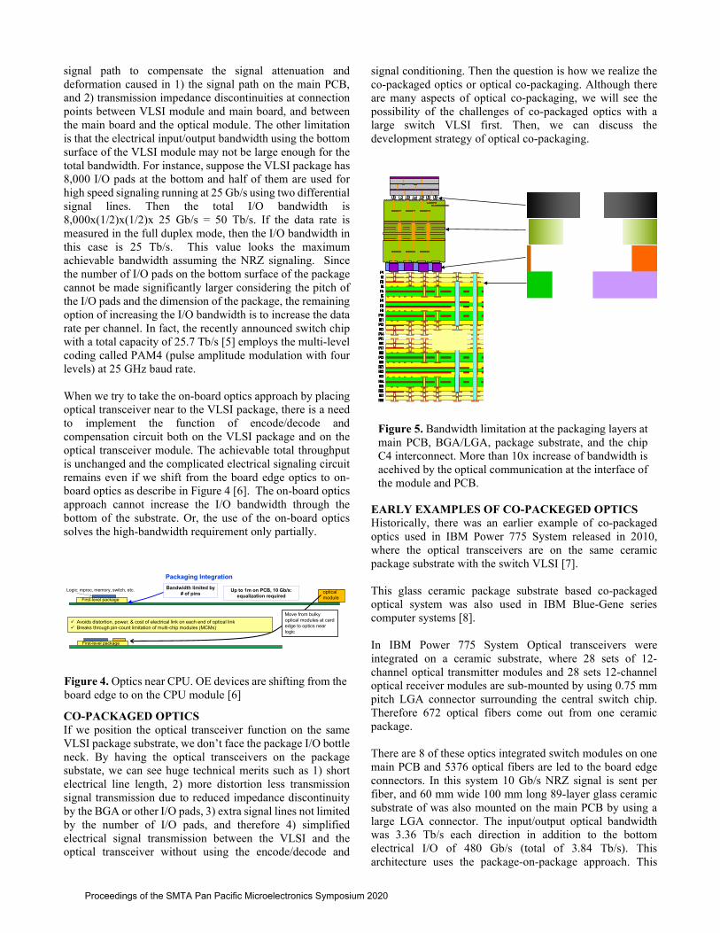
Figure 5. Bandwidth limitation at the packaging layers at main PCB, BGA/LGA, package substrate, and the chip C4 interconnect. More than 10x increase of bandwidth is acehived by the optical communication at the interface of the module and PCB.
Proceedings of the SMTA Pan Pacific Microelectronics Symposium 2020
package structure is considered the first example of co-packaged optics with a large VLSI, where we can enjoy all the benefit which optical co-packaging offers. This co-packaged optics performed as expected.
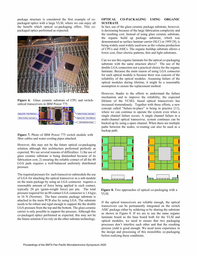
However, this may not be the future optical co-packaging solution although this architecture performed perfectly as expected. We see several reasons of difficulties: 1) the use of glass ceramic substrate is being diminished because of its fabrication cost; 2) ensuring the reliable contact of all the 80 LGA pads requires a well-balanced uniformly distributed pressure. The required pressure for each transceiver submodule the use of LGA for attaching the optical transceiver as a sub-module on the main package by using an LGA connector requires a reasonable amount of force being applied to each contact, typically 20 gw (gram-weight force) per pin. The total pressure required for an 80 contact LGA connector is 1.6 kgw, or 16 N (Newton). The base ceramic package substrate is attached to the main PCB also by using LGA. The substrate needs to be robust and rigid enough to support the the double LGA pressure from the top and the bottom. The glass ceramic carrier is only possible to support the pressure. Although this co-packaged optics performed as expected, this may not be the future solution if we rely on the other substate technology.
OPTICAL CO-PACKAGING USING ORGANIC SUSTRATE In fact, use of the glass ceramic package substrate, however, is decreasing because of the large fabrication complexity and the resulting cost. Instead of using glass ceramic substrate, the organic build up package substrate, which was demonstrated as surface laminar carrier (SLC) in 1995 [9], is being widely used widely used now as the volume production of CPUs and ASICs. The organic buildup substrate allows a lower cost, finer electric patterns, thin and light substrates. Can we use this organic laminate for the optical co-packaging substrate with the same structure above? The use of the double LGA connectors not a practical choice for the organic laminate. Because the main reason of using LGA connector for each optical module is because there was concern of the reliability of the optical modules. Assuming failure of the optical modules during lifetime, it might be a reasonable assumption to ensure the replacement method. However, thanks to the efforts to understand the failure mechanism and to improve the reliability, the expected lifetime of the VCSEL based optical transceivers has increased tremendously. Together with these efforts, a new concept called “failure-in-place” is being in practice [11], where we can continue to operate the system even when a single channel failure occurs. A single channel failure in a multi-channel optical transceiver, system continues can be backed up by using a spare channel. When there are multiple paths between the nodes, re-routing can also be used as a backup path.
If the optical transceivers are reliable enough, the optical transceivers can be permanently integrated on the switch ASIC package either by soldering or by sharing the substrate as shown in Figure 8. If we are to use the same organic laminate board as the base board both for the VLSI and optical modules, we need to ensure that two packaging processes don’t interfere each other and that the resulting process yield is good enough. We need more experience in the design and processing of this monolithic co-packaging before realizing these conditions.
Water Cooling - Input pipe
Water Cooling - Input pipe
Optical I/Os – Fiber Ribbons
Optical I/Os – Fiber Ribbons
LGA Hold-Down Clamp
Figure 8. Two approaches of optical co-packaging with a VLSI.
Figure 6. Glass ceramic substrate of CPU and switch-optical transceivers in IBM Power 775.
Figure 7. Photo of IBM Power 775 switch module with fiber cables and water-cooling pipes attached.
Proceedings of the SMTA Pan Pacific Microelectronics Symposium 2020

At present the most practical approach is considered to be the solder mounting of finished optical submodules onto the VLSI carrier substrate. By doing this we can only use well tested known-good optical modules for the assembly [12]. This approach is called “hybrid co-packaging” in this paper. HYBRID OPTICAL CO-PACKAGING APPROACH There are several test cases to see how we can configure the optical co-packaging with a VLSI. One is a co-packaging with a CPU. The other is with a switch VLSI chip. As shown in Figure 9, the same optical transceiver submodules can be used both for the CPU and the switch modules. The switch modules are more demanding in terms of number of ports, or number of fibers.
If a single port has a bandwidth of 400 Gb/s and one switch supports total 64 ports, where each port corresponds to one transceiver, we can configure one server rack consisting of 32 servers and one switch located at the top of the rack, where 32 ports of the switch are linked to 32 servers one-by-one, and the remaining 32 ports are individually connected to 16 spine switches as shown in Figure 9. If we utilize the 25.6 Tb/s switch chip with integrated optical transceivers discussed earlier as the switch module, 64 sets of 400 Gb/s optical transceivers are placed around the switch VLSI on the package substrate. Suppose each lane of the transceiver transmits 50 Gb/s of signal, 16 fiber lanes need to be used for a transceiver with 400 Gb/s total bandwidth. Then 1024 fibers need to be connected to the package. A possible configuration of such a optically co-packaged switch module is placing 22 units of 48-channel optical transceivers around the central switch chip. We already proposed a design of this type of VCSEL based transceiver [10]. This submodule design assumes use of standard 12 channel VCSELs, photodiodes, driver and TIA chips with a combination of tight pitch polymer waveguides, if the data
channels are all transmitted through the on-package optical transceivers. A design of this optical transceiver is shown in Figure 10 and the its prototype is shown in Figure 11 [11]. Since the transceiver is placed close to the VLSI, which is the data source and sink, we can simplify the signal conditioning and error correction circuit on the optical transceiver submodules.
Optical fiber cables need be detached from the transceiver submodule for handling the module. The ideal case is that the complete module only has electrical and optical contacts or connectors and sufficient cooling is made. The simplest way of multi-channel optical connector is to make the module to have a short pigtail like cable with the parallel optical connector such as MTP at the end as shown in the rightmost picture of Figure 11. For a small optical channel application, this might be acceptable, however, handling of many fibers may cause a difficulty. For the large fiber count package, optical fibers need to be detached at the peripheries of the package [13]. Three connector locations can be thought of: 1) top, 2) bottom and 3) side. The packaged VLSI is usually cooled from the top surface of the package. Therefore, the optical connectors have to be at the very edge of the package so that the cooling system does not interfere. The side of the package is a location compatible with other constrain but the package has to be thicker than the connector. The bottom of the package is compatible with the cooling and allocation of the area to
CPU & TRxs
TRx2
TRx1
Server Main Board
Mem
ory CPU
Switch VLSI
Switch VLSI
Switch VLSI
Switch VLSI
Switch VLSI
CPU & TRxs
TRx2
TRx1
Server Main Board
Mem
ory CPU
CPU & TRxs
TRx2
TRx1
Server Main Board
Mem
ory CPU
CPU & TRxs
TRx2
TRx1
Server Main Board
Mem
ory CPU
CPU & TRxs
TRx2
TRx1
Server Main Board
Mem
ory CPU
CPU & TRxs
TRx2
TRx1
Server Main Board
Mem
ory CPU
Switch VLSI
Switch VLSI
Switch VLSI
Switch VLSI
Switch VLSI
Switch VLSI
Switch VLSI
Switch VLSI
Switch VLSI
Switch VLSI
Switch VLSI
Switch VLSI
Switch VLSI
Switch VLSI
Switch VLSI
Switch VLSI
Switch VLSI
Switch VLSI
Switch VLSI
Switch VLSI
Switch VLSI
Switch VLSI
Switch VLSI
Switch VLSI
Switch VLSI
Switch VLSI
Switch VLSI
Switch VLSI
Switch VLSI
Switch VLSI
Switch VLSI
Switch VLSI
Switch VLSI
Switch VLSI
Switch VLSI
CPU & TRxs
TRx2
TRx1
Server Main Board
Mem
ory CPU
Switch VLSI
Switch VLSI
Switch VLSI
Switch VLSI
Switch VLSI
CPU & TRxs
TRx2
TRx1
Server Main Board
Mem
ory CPU
CPU & TRxs
TRx2
TRx1
Server Main Board
Mem
ory CPU
CPU & TRxs
TRx2
TRx1
Server Main Board
Mem
ory CPU
CPU & TRxs
TRx2
TRx1
Server Main Board
Mem
ory CPU
CPU & TRxs
TRx2
TRx1
Server Main Board
Mem
ory CPU
Switch VLSI
Switch VLSI
Switch VLSI
Switch VLSI
Switch VLSI
CPU & TRxs
TRx2
TRx1
Server Main Board
Mem
ory CPU
Switch VLSI
Switch VLSI
Switch VLSI
Switch VLSI
Switch VLSI
CPU & TRxs
TRx2
TRx1
Server Main Board
Mem
ory CPU
CPU & TRxs
TRx2
TRx1
Server Main Board
Mem
ory CPU
CPU & TRxs
TRx2
TRx1
Server Main Board
Mem
ory CPU
CPU & TRxs
TRx2
TRx1
Server Main Board
Mem
ory CPU
CPU & TRxs
TRx2
TRx1
Server Main Board
Mem
ory CPU
Switch VLSI
Switch VLSI
Switch VLSI
Switch VLSI
Switch VLSI
Switch VLSI
Switch VLSI
Switch VLSI
Switch VLSI
Switch VLSI
Switch VLSI
Switch VLSI
Switch VLSI
Switch VLSI
Switch VLSI
Switch VLSI
Switch VLSI
Switch VLSI
Switch VLSI
Switch VLSI
Switch VLSI
Switch VLSI
Switch VLSI
Switch VLSI
Switch VLSI
Switch VLSI
Switch VLSI
Switch VLSI
Switch VLSI
Switch VLSI
Switch VLSI
Switch VLSI
Switch VLSI
Switch VLSI
Switch VLSI
Switch VLSI
Switch VLSI
Switch VLSI
Switch VLSI
Switch VLSI
Switch VLSI
Switch VLSI
Switch VLSI
Switch VLSI
Switch VLSI
Switch VLSI
Switch VLSI
Switch VLSI
Switch VLSI
Switch VLSI
Switch VLSI
Switch VLSI
Switch VLSI
Switch VLSI
Switch VLSI
Switch VLSI
Switch VLSI
Switch VLSI
Switch VLSI
Switch VLSI
Switch VLSI
Switch VLSI
Switch VLSI
Switch VLSI
Switch VLSI
……
Figure 9. Densely interconnected servers in advanced data center. Both CPU modules and switch modules obtain benefit of optical co-packaging. This network structure is one of the target applications of the Motion project [11].
Figure 10. A possible layout of high density 48 channel optical transceiver. By using a tight pitch polymer optical waveguide, a compact optical routing can be realized.
Figure 11. A prototype high density optical transceiver. Two 12-channel VCSEL arrays and two 12-channel PD arrays are used in combination with the polymer waveguide optical routing component.
Proceedings of the SMTA Pan Pacific Microelectronics Symposium 2020

optical connection. because it does not interfere with the top cooling system and optical connector occupies 1/10 area of 0.5 mm pitch BGA electrical connector and some of electrical high speed interconnects at the bottom of the package are replaced by optical links assuming that the area of 48 channel MT ferrule is 15 mm2 and one differential electrical signal pair occupies 3 mm2. Application of optical co-packaging to CPU module is less demanding because the number of fiber channels are less and therefore the total package area is smaller. As the requirement of the optical transceiver performance per link is the same for the CPU module and the switch module is the same, optical co-packaging technology is equally usable to both of the CPU and the switch module applications. We assumed use of multimode fibers here. Further study will be needed to realize single mode optical transceiver submodule [15. 16]. REALIZATION OF OPTICAL CO-PACKAGING We can design a practical optical co-packaging with a VLSI based on the above discussion. As the optical transceiver fabrication requires special fabrication process steps different from the electronic packaging, attaching optical transceiver submodules onto the VLSI packaging substrate is more practical. This also solves the yield loss related to non-standard optical packaging. The most realistic approach of optical co-packaging with a VLSI is soldering completed optical submodules onto the VLSI packaging substrate for the sake of space, cost, reliability and performance. Soldering of components onto the VLSI substrate usually requires solder reflow process and following flux cleaning process. However, solder mounting of optical transceiver submodules is different. We cannot use water cleaning of flux and the sensitive optical surfaces have to be protected during reflow or soldering process. This is particularly true for the optical connector contacting surface. The optical submodules also have to be tolerant to the reflow temperature. If the optical transceiver is the final product, the optical packaging including optical connector attachment can be the last process after solder process is finished. In the case of submodule soldering, the submodule is inevitably exposed to the soldering temperature. Since the atmosphere during the soldering possibly affects the sensitive optical surface, protection such as using a sacrificial protective coating is required. SUMMARY Technology related to optical co-packaging of VLSI is discussed. A practical approach of the optical co-packaging is to use optical transceiver submodules and to attach them onto the package substrate by soldering. Although some of the key concepts and key components were shown feasible, more detailed study of the design, process and materials is necessary. Particularly, because some surface of the package
is optical path and requires protection from the environment during fabrication process, the material and package design require further investigation. ACKNOWLEDGEMENT The author thanks Daniel Kuchta, Hidetoshi Numata, both IBM Research, and Nicolas Boyer, IBM Canada for fruitful discussion.
REFERENCES 1. D. Chen, et al. "Looking under the hood of the IBM
Blue Gene/Q network" in SC'12: Proceedings of the International Conference on High Performance Computing, Networking, Storage and Analysis. IEEE, 2012.
2. Y. Ajima, et al.: “The Tofu interconnect” in 2011 IEEE 19th Annual Symposium on High Performance Interconnects
3. Y. Ajima, et al. "The tofu interconnect D." 2018 IEEE International Conference on Cluster Computing (CLUSTER). IEEE, 2018.
4. https://www.gigalight.com/show-654.html (400G/200G optical transceivers)
5. https://www.broadcom.com/company/news/product-releases/52756 (Broadcom 25.7 Tb/s switch chip)
6. C. Schow: “Power Efficient Tb/s Optical Interconnects,” Frontier in Optics 2012 (October 16) OSA, 2012
7. http://www.redbooks.ibm.com/redbooks/pdfs/sg248003.pdf (IBM Power 775 Redbook)
8. J. Kahle, et al.. "2.1 Summit and Sierra: Designing AI/HPC Supercomputers." 2019 IEEE International Solid-State Circuits Conference-(ISSCC). IEEE, 2019. (Summit)
9. Y. Tsukada, et al.: "Surface laminar circuit packaging." 1992 Proceedings 42nd Electronic Components & Technology Conference. IEEE, 1992.
10. H. Numata, et al.: “60-Micrometer pitch polymer waveguide array attached active optical flex.” 2017 Optical Fiber Communications Conference and Exhibition (OFC) pp. 1-3 (2017, March) IEEE.
11. D. Kuchta, et al. "Multi-wavelength optical transceivers integrated on node (MOTION)." 2019 Optical Fiber Communications Conference and Exhibition (OFC). IEEE, 2019.
12. Y. Taira: "Integration of optical interconnect for servers: Packaging approach toward near-CPU optics." 2017 International Conference on Electronics Packaging (ICEP). IEEE, 2017.
13. Y. Taira, et al. "OE device integration for optically enabled MCM." 2007 Proceedings 57th Electronic Components and Technology Conference. IEEE, 2007.
14. T. Barwicz, “An O-band Metamaterial Converter Interfacing Standard Optical Fibers to Silicon Nanophotonic Waveguides,” 2015 OFC (2015).
15. T, Barwicz, and Y. Taira, “Low-Cost Interfacing of Fibers to Nanophotonic Waveguides: Design for Fabrication and Assembly Tolerances,” IEEE Photonics Journal, 66008818 Vol. 6 No.4 (2014).
Proceedings of the SMTA Pan Pacific Microelectronics Symposium 2020