Technical Manual TRANSDUCER AMPLIFIER TYPE · PDF fileRDP Customer Document Technical Manual...
16
RDP Customer Document Technical Manual TRANSDUCER AMPLIFIER TYPE S7DC Doc. Ref CD1202Z This manual applies to units of mod status 8 ONWARDS BS EN ISO 9001 Certificate No. FM13141 Affirmed by Declaration of Conformity USA & Canada All other countries RDP Electrosense Inc. RDP Electronics Ltd 2216 Pottstown Pike Pottstown, PA 19465 U.S.A. Grove Street, Heath Town, Wolverhampton, WV10 0PY United Kingdom Tel (610) 469-0850 Fax (610) 469-0852 Tel: +44 (0) 1902 457512 Fax: +44 (0) 1902 452000 E-mail [email protected] www.rdpe.com E-mail: [email protected] www.rdpe.com
Transcript of Technical Manual TRANSDUCER AMPLIFIER TYPE · PDF fileRDP Customer Document Technical Manual...

RDP Customer Document
Technical Manual
TRANSDUCER AMPLIFIER TYPE S7DC
Doc. Ref CD1202Z
This manual applies to units of mod status 8 ONWARDS
BS EN ISO 9001 Certificate No. FM13141
Affirmed by Declaration of Conformity
USA & Canada All other countries
RDP Electrosense Inc. RDP Electronics Ltd
2216 Pottstown Pike Pottstown, PA 19465
U.S.A.
Grove Street, Heath Town, Wolverhampton, WV10 0PY
United Kingdom
Tel (610) 469-0850 Fax (610) 469-0852
Tel: +44 (0) 1902 457512 Fax: +44 (0) 1902 452000
E-mail [email protected] www.rdpe.com
E-mail: [email protected] www.rdpe.com

2
INDEX
1 INTRODUCTION ..................................................................................................... 3 1.1 Certificate of EMC conformity .................................................................................. 4
2. INSTALLATION ....................................................................................................... 5
3. CONNECTIONS ...................................................................................................... 6 3.1 Supply / output connections .................................................................................... 6
3.2 Transducer connections .......................................................................................... 7 3.3 Full bridge Strain Gauge Transducer ...................................................................... 7 3.4 1/4 or 1/2 bridge transducer connections ................................................................ 7 3.5 Potentiometric Transducers .................................................................................... 7
4. CONTROLS ............................................................................................................ 9
4.01 Output Mode Link: ................................................................................................... 9
4.02 Excitation ................................................................................................................ 9 4.03 Zero ......................................................................................................................... 9
4.04 Fine Gain ................................................................................................................ 9 4.05 Gain Range (x1 to X1250) ...................................................................................... 9 4.06 Shunt Calibration ..................................................................................................... 9
4.07 Bandwidth/Noise Capacitor ................................................................................... 10 4.08 4-20mA Offset Solder Link SP1 ............................................................................ 10 4.09 Relay Voltage Solder Link SP2 ............................................................................. 10
4.10 Maximum Voltage output vs. Supply Voltage. ....................................................... 10 4.11 Maximum 4-20mA loop resistance Vs. Supply Voltage. ........................................ 10
5. SETTING-UP PROCEDURE, Voltage Output ....................................................... 11
6. SETTING-UP PROCEDURE, 4-20mA Output ...................................................... 11
7. SHUNT CALIBRATION FACILITY ........................................................................ 12
8. SPECIFICATION ................................................................................................... 13
9. FUNCTIONAL CHECKS ....................................................................................... 15
10 WARRANTY AND SERVICE ................................................................................ 16
TABLE OF FIGURES Fig. 1 Connections & Control Locations .......................................................................... 5
Fig. 2 Signal Cable Installation for Optimum EMC .......................................................... 8

3
1 INTRODUCTION The S7DC is an in-line d.c. amplifier intended to provide variable excitation and signal amplification for strain gauge type transducers. It will operate from unregulated single or dual tracking power supplies and provide up to 10V output (or 4-20mA) with transducer signals from 10mV to 10V. This allows operation with some high output transducers (DCT, etc.); for example, to provide 4-20mA outputs with signal inputs up to 10V. This unit accepts both uni-polar (eg 0 to 4mV) or bi-polar (eg ± 4mV) input signals and can produce corresponding uni-polar or bi-polar voltage outputs (ie 0 to 10v or ±10v) sensitivities and gains given in this document refer to both. Current outputs (4 to 20mA) are uni-polar. Excitation, coarse gain, fine gain and fine zero controls are provided, with the facility to connect remotely an internal shunt calibration resistor. Connections are made via screw-terminals which, with the controls, are all mounted inside an aluminium case, sealed to IP65 specification. Note that the voltage output common (0v terminal) with a single (2 wire) supply voltage, is approximately at the mid supply voltage eg with a 24 volt supply the output common is 12 volts (see section 3.1).

4
1.1 Certificate of EMC conformity
DECLARATION OF CONFORMITY
RDP ELECTRONICS LTD. Grove Street Heath Town
Wolverhampton West Midlands WV10 0PY
United Kingdom
We declare that the product described in this technical manual is manufactured by RDP Electronics Limited and performs in conformity
to the following:
The Electromagnetic Compatibility Directive 2014/30/EU
RoHS2 Directive 2011/65/EU
R D Garbett Director
RDP Electronics Limited

5
F C
J1
RV1 B A
B A
SP2
CON2 SUPPLY/OUTPUT
R21 SW1 GAIN
CON1 TRANSDUDER
GND
V+
0V
V-
OUT
RCAL
EXC+
EXC-
SIG+
SIG-
SCN
CAL
Transducer Excitation
Signal
Cable Shield/Screen
F.GAIN
RV3
SP1
RV
2
V mA
OUTPUT EXCIT
C2
Shunt Calibration
Ground
Supply Positive
Output/Dual Supply Common
Supply Negative
Output (V or I)
Remote Shunt Calibration
ZERO
2. INSTALLATION 2.1 For EMC compliance, only multi-core cables should be used for the signal input and
output connections. 2.2 The shields of the two cables may be connected to the SCN and common terminals
of the transducer connector and output connector but, for optimum EMC, the cable shield should be terminated as shown in Fig.2
2.3 ESD precautions should be used when working on the instrument with the lid
removed. The user should ensure he is "grounded" by use of an grounded wrist strap or at least touching ground before touching any component, including wires, terminals or switches.
2.4 Segregate signal/supply/output cables. Route signal cables away from possible
sources of EMI, e.g. motor/solenoid/relay cables, etc. 2.5 The transducer body should be grounded. The transducer body being clamped or
bolted to grounded metalwork, e.g. on a machine usually achieves this. Where this does not apply and also where there is no grounding connection via the connection cable to the S7DC, then a separate grounding wire should be connected from the transducer body to the S7DC SCN terminal.
2.6 Ground the case, e.g. via the mounting holes provided.
Fig. 1 Connections & Control Locations

6
GROUND
V+
0V
V-
OUTPUT
R CAL
V+ (+10 to +36V)
V- ±3V to ±10V
-
+
GROUND
V+
0V
V-
OUTPUT
R CAL
V+ (+5 to +18V)
(0V)
V- (-5 to -18V) ±3V to ±10V
-
+
GROUND
V+
0V
V-
OUTPUT
R CAL
V+ (10 to 36V)
V- 4 to 20 mA
+
-
3. CONNECTIONS 3.1 Supply / output connections a) Voltage output, single supply. This arrangement should only be used if (b) is not possible.
If this arrangement is used, either the supply V- or the output common 0V (or both) must be fully floating ie only one can be grounded. Failure to do this may result in damage to the amplifier that is not covered by warranty.
b) Voltage output, dual supply (supply must be symmetrical)
Either the supply V- or the output common 0V (or both) must be fully floating ie only one can be grounded. Failure to do this may result in damage to the amplifier that is not covered by warranty.
c) Current output, single supply. Ensure that the output mode link (J1) is set to mA. See Fig. 1 for location.
Note 1 Ground is connected to the case of the amplifier.

7
EXC-
A
B C
D
EXC+
SIG+ SIG-
EXC+
SIG+
SIG-
EXC-
R24
POTENTIOMETER
3.2 Transducer connections Before connecting the transducer, check the excitation voltage. Applying an excitation voltage that is too high may destroy the transducer
3.3 Full bridge Strain Gauge Transducer Transducer connector details are as shown in Fig. 1 and on the S7DC circuit board. To use the shunt calibration facility, insert a link between 'CAL' and 'SIG-'.
3.4 1/4 or 1/2 bridge transducer connections For 1/4 bridge transducers, 3 bridge completion resistors are required. The active gauge should be fitted on arm 'C' and the bridge completion resistors in arms D, A & B. For 1/2 bridge systems, the active gauges should be C and D, and 2 completion resistors are required. The bridge completion resistors should be high stability, the same resistance as the active gauge and may be fitted either in the transducer connector, or in the designated position on the underside of the S7DC PCB. This requires removal of the PCB from the case. R22 replaces bridge arm D, R23 replaces bridge arm A, R24 replaces bridge arm B Note: Mounting these resistors in the instrument is a compromise. To reduce temperature
and long lead effects, completion resistors should preferably be mounted at the transducer and be of close tolerance and low t.c., e.g. 0.1%, 15 ppm..
3.5 Potentiometric Transducers Select R24 value to drop at least 1.5V. For example, with an excitation of say 10V and a potentiometer resistance of 500 ohms and R24 value of 100 Ohms, the voltage drop across R24 = 10V / (500+100) X 100 = 1.7V. This raises terminal 4 to within the common mode voltage range of the amplifier.
Input signal = 10-1.7 = 8.3V so use the lowest gain range for ±10V output. For lower output voltage or 4-20mA output, use lower excitation, e.g. 5V. R24 can be added either in the solder pins on the underside of the PCB, or more easily into the transducer screw terminals, between 'SIG-' and 'EXC-'
8
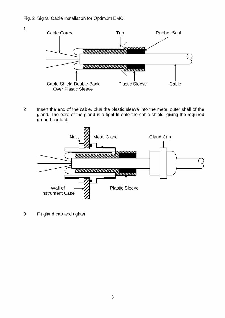
Cable Cores Trim Rubber Seal
Cable Shield Double Back Over Plastic Sleeve
Plastic Sleeve Cable
Gland Cap
Plastic Sleeve
Metal Gland Nut
Wall of Instrument Case
Fig. 2 Signal Cable Installation for Optimum EMC 1
2
Insert the end of the cable, plus the plastic sleeve into the metal outer shell of the gland. The bore of the gland is a tight fit onto the cable shield, giving the required ground contact.
3 Fit gland cap and tighten

9
4. CONTROLS 4.01 Output Mode Link: The "OUTPUT" jumper link is set to "V" for voltage output or "mA" for current output.
Three 20-turn screwdriver-adjusted controls are provided for controlling: 4.02 Excitation - allowing continuous variation of excitation between 3v and 10v. Note: if supply is
<13V, the max. excitation voltage available is Vs - 3V. Note: for units of MOD18 onward, if operating temperature exceeds 70°C then the maximum current is 60mA,
4.03 Zero - allowing a fine adjustment of output zero of approximately ±2V (or 0-10mA)
depending on Fine Gain setting. 4.04 Fine Gain - allowing a 4:1 variation in amplifier gain, used in conjunction with 4.05. 4.05 Gain Range (x1 to X1250)
- sliders 1 to 4 of the 6-slider DIL switch, when used with the fine gain control, provide an output of 5V or 4-20mA with an input signal range of approx. 4mV to 5V as shown below:
(also output ± 5v for input ±4 mV to ±5v).
SLIDERS ON
For Mod.8 (and above) For ±10V OUTPUT INPUT SIGNAL RANGE for: 5V or 4-20mA OUTPUT
4 + 3 + 2 4 – 16mV ±8 to ±32mV
4 + 3 5 – 20mV ±10 to ±40mV
4 + 2 18 – 70mV ±35 to ±140mV
4 + 1 65 – 270mV ±130 to ±500mV
4 0.25 – 1V ±0.5 to ±2V
1 0.34 – 1.35V ±0.7 to ±2.7V
None 1.25 – 5V ±2.5 to ±10V
Note: for the two lowest gain ranges (with slider 4 off), the excitation voltage must be 5V to provide signals within the required common mode voltage range of the amplifier.
Note: for ±10v output, the supply must be at least 22v or ±11v (see 4.10). 4.06 Shunt Calibration - slider 5 ("C") of the 6-slider DIL switch, when set to ON connects an internal 59kΩ
0.1% resistor across one arm of the bridge. Remote Cal. - an internal relay may be used to remotely connect the 59kΩ resistor. To operate this relay, connect the R-Cal. terminal to V- (CON 2) at any convenient point (lead length is irrelevant) via a switch, etc. Note 1: For normal relay operation, the supply voltage must be at least 15V. For lower supply voltages, solder link SP2 must be made (see Fig.1). Note 2: For normal shunt calibration, connect the CAL terminal to Sig- (CON 1). This links the internal calibration resistor (terminal 6) to the relevant bridge node.

10
If long cables are used, then cable voltage drop may cause significant shunt calibration errors. In this case, do not link 4 to 6 but connect terminal 6 via a separate wire to the relevant bridge node as near as possible to the transducer. Calibration Resistor. The 59kΩ resistor (R21) is mounted on pins for ease of changing. 4.07 Bandwidth/Noise Capacitor - slider 6 ("F") of the 6-slider DIL switch, when set to ON, connects capacitor C2 to
reduce output noise (and bandwidth). C2 is mounted on pins for convenience. Its location is shown in Fig.1. The value is normally 47nF for standard bandwidth (BW) and noise specifications. BW is roughly inversely proportional, e.g. to halve BW (and noise) change C2 to 100nF.
4.08 4-20mA Offset Solder Link SP1 Normally, with SP1 not fitted, the relationship between signal/voltage output/current
output is:- Zero to F.S. signal 0 to 5V or 4-20mA output.
For low supply voltage applications (<14v) or bipolar operation, e.g. for compressive/tensile load applications, SP1 may be fitted which changes the relationship to: ±F.S. signal = ±2.5V or 4-20ma output. i.e. SP1 provides a ½ F.S. offset for the current output and increases the voltage head room in the amplifier.
4.09 Relay Voltage Solder Link SP2
(Refer also to Section 4.06)
Solder link SP2 changes the supply voltage required for local or remote operation of the shunt calibration relay as detailed in the specification, Section 8.
Units are normally supplied with SP2 not linked.
4.10 Maximum Voltage output vs. Supply Voltage.
As well as having absolute maximum and minimum values as defined in the specification, the maximum output voltage is supply dependent and relates as follows: -
Max output = (Total supply Voltage - 2) / 2,
E.g. for an 18V (or 9V dual rail) supply, = (18-2) / 2 = ±8V maximum output. 4.11 Maximum 4-20mA loop resistance Vs. Supply Voltage.
The maximum permissible 4-20mA loop resistance depends upon the supply voltage to the S7DC unit. Please note, and do not exceed the maximum supply voltage detailed in the specification.
Max loop resistance = ((Total supply Voltage - 12) x 25 ) + 100 E.g., at 10V supply, = ((10 - 12) x 25) + 100 = 50 Ohms

11
5. SETTING-UP PROCEDURE, Voltage Output (OUTPUT jumper set to "V") Refer also to Section 7 for Shunt Calibration Method.
5.1 Determine the transducer bridge output from the manufacturer's data sheet and
adjust the coarse gain control as shown in Section 4.05. Check that sliders 5 and 6 are set to OFF.
5.2 Connect the monitor and supply as detailed in Sections 2 and 3. With transducer
DISCONNECTED switch ON power. Set excitation voltage, via the EXCIT control, to the value indicated in the transducer data.
Note, excessive excitation voltage or incorrect connection may irreparably damage the transducer.
Connect transducer and allow a 20-minute warm-up period (for maximum accuracy) 5.3 With zero load (pressure, etc.) applied to the transducer, adjust the ZERO control
for zero output. 5.4 Apply a precise load (pressure, etc.) to the transducer and adjust the F.GAIN
control for the desired output. 5.5 Repeat steps 3 and 4 until repeatable readings are obtained. 5.6 Operate the Cal. switch or Remote Cal. (Sections 4.06 and 7) and note output for
future reference.
6. SETTING-UP PROCEDURE, 4-20mA Output 6.1 Check that the OUTPUT jumper link is set to "mA". Refer to Section 4.08 for bipolar
input signal operation. 6.2 Proceed with 5.1 and 5.2 above, then: 6.3 With transducer output approximately zero, adjust the ZERO control for an output
current of 4mA approx. 6.4 Apply a known value to the transducer and adjust FINE GAIN for the desired output
(preferably full scale for 20mA output). Repeat steps 3 & 4 for consistent results. 6.5 Operate the Cal. switch or Remote Cal. (see Section 4.06) and note output for
future reference. Refer to Section 7. Reference may be made to Section 7.2 but note that full scale of output is 20-4 = 16mA.

12
7. SHUNT CALIBRATION FACILITY Refer to Section 4.06 for Operation
This is applicable to resistance bridge transducers only, e.g. most load cells and pressure transducers (not semi-conductor gauges).
The Shunt Calibration Facility can be used as:-
7.1 A Calibration Check. When the prime calibration has been made by applying a
precise known pressure or load to the transducers as described in Section 5 or 6, the R-CAL relay can be operated (normally with zero pressure or load applied) and the output recorded as the Calibration Check figure. A quick check can then be made at anytime by comparing new CAL outputs with the original.
Note that if the output is not at zero when the CAL switch is operated, the true CAL CHECK figure is the CAL output less the initial output.
7.2 A Shunt Calibration. The shunt calibration method can be used to calibrate the
transducer and electronics without having to apply a known pressure or load to the transducer.
7.2.1 Calculate the shunt calibration figure required from the data given on the transducer
Calibration Record Sheet (CRS). From CRS - output for 100% = WmV - output with shunt = YmV Therefore output required in CAL is Y/W x required full scale output. Note: If CRS states shunt resistor different from the one fitted (59k ohm is
standard, other values to order) then it may still be possible to obtain a calibration from:
CAL figure calculated x (R shunt / 59k) = new CAL figure
7.2.2 Set the COARSE GAIN switch for the required input sensitivity (see Section 4.5). 7.2.3 Connect the monitor and supply as detailed in Sections 2 and 3. With transducer
DISCONNECTED switch ON power. Set excitation voltage, via the EXCIT control, to the value indicated in the transducer data.
Note, excessive excitation voltage or incorrect connection may irreparably damage the transducer. Connect transducer and allow a 20-minute warm-up period (for maximum accuracy)
7.2.4 Ensure no load or pressure applied to the transducer. 7.2.5 Operate CAL relay and adjust FINE GAIN control to give the required output as
calculated in 7.21.

13
8. SPECIFICATION Supply Voltage 1. 10 to 36V or 2. ±5V to ±18V. Refer to “Output” and
“Temperature Range” below
Supply Current 30mA + Excitation Load + Output Current typical + CAL relay.
Output 1. ±3V to ±10V max. according to supply voltage. See Sect
4.10 into 2k (dual supply) or 10k (single supply).
2. 4-20mA into 0-800 . depending on supply. See Sect 4.11 This is an active output that should not be connected to any external power supply as this will damage unit.
Excitation
Voltage 3 to 10V (Supply Voltage = 13-36V) continuously variable at 100mA max (See Section 4.02)
Regulation Excitation change = 0.2% typ with supply change 21-36V Excitation change = 0.10% typ with load change 0-100 mA
Tempco 0.005%/°C typical
Amplifier
Linearity 0.02% of FS output
Bandwidth 5kHz typical (See Section 4.07) 20Hz with filter ON.
Noise 10mV or 30µA p-p (less with filter ON) typical
Zero Tempco 0.002% FS/°C typical (optimum at ±10V o/p)
Gain Tempco 0.003% FS/°C typical (optimum at ±10V o/p)
Regulation For symmetrical supply, change when gain = 250. Voltage o/p = 2 mV/V, current o/p = 10µA/V. For an asymmetrical supply change when gain = 250. This is not recommended up to mod state 18C. For mod state 19 onwards, voltage o/p = 34m V/V current o/p = 170µA/V. (see also excitation regulation above).
Input Impedance >10M ohm
CMRR 95dB typical, dc to 50Hz
Zero Adjustment ±2V (or 0-10mA) output typical. Depends on Fine Gain setting.
Sensitivity Range 4mV – 10V input for 5V (or 20mA) output in 6 ranges with 4:1 Fine Gain Control (Gain range x1 to x1250). See Section 4.05.
14
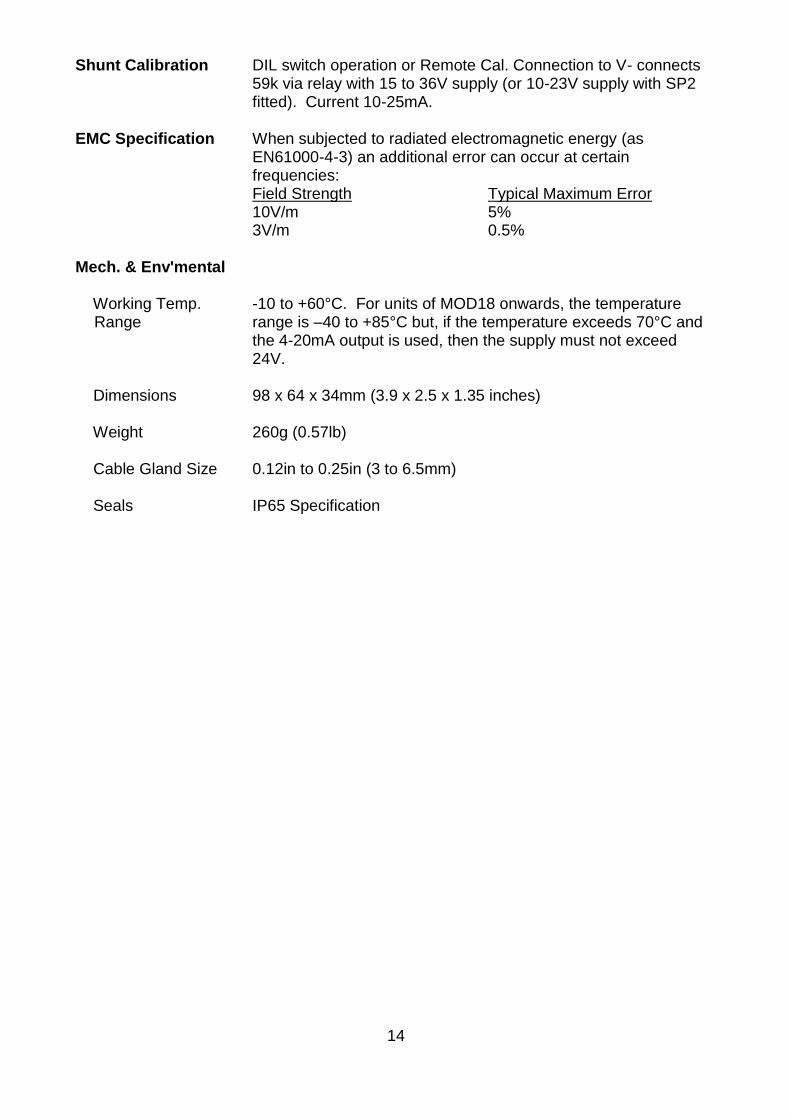
Shunt Calibration DIL switch operation or Remote Cal. Connection to V- connects 59k via relay with 15 to 36V supply (or 10-23V supply with SP2 fitted). Current 10-25mA.
EMC Specification When subjected to radiated electromagnetic energy (as EN61000-4-3) an additional error can occur at certain frequencies:
Field Strength Typical Maximum Error 10V/m 5% 3V/m 0.5%
Mech. & Env'mental
Working Temp. Range
-10 to +60°C. For units of MOD18 onwards, the temperature range is –40 to +85°C but, if the temperature exceeds 70°C and the 4-20mA output is used, then the supply must not exceed 24V.
Dimensions 98 x 64 x 34mm (3.9 x 2.5 x 1.35 inches)
Weight 260g (0.57lb)
Cable Gland Size 0.12in to 0.25in (3 to 6.5mm)
Seals IP65 Specification
15
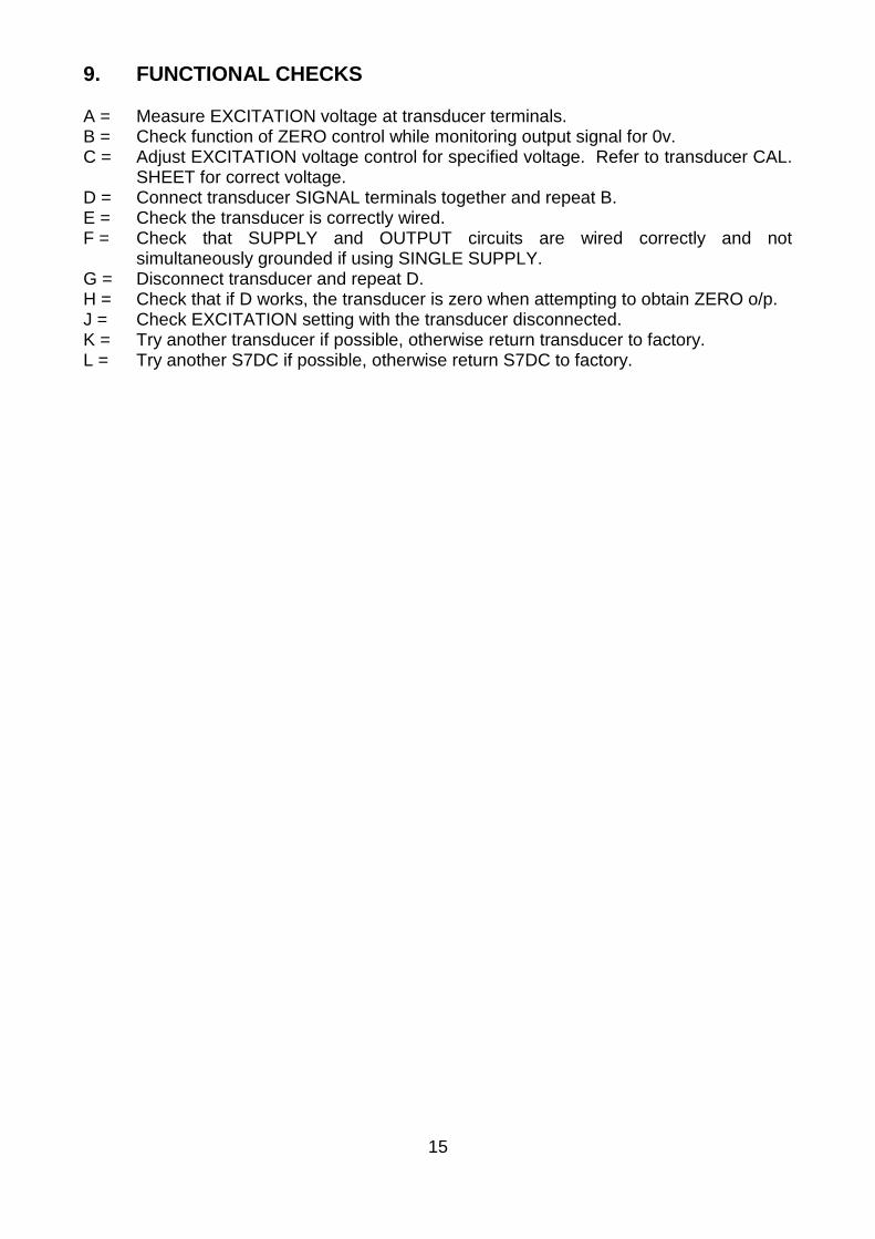
9. FUNCTIONAL CHECKS A = Measure EXCITATION voltage at transducer terminals. B = Check function of ZERO control while monitoring output signal for 0v. C = Adjust EXCITATION voltage control for specified voltage. Refer to transducer CAL.
SHEET for correct voltage. D = Connect transducer SIGNAL terminals together and repeat B. E = Check the transducer is correctly wired. F = Check that SUPPLY and OUTPUT circuits are wired correctly and not
simultaneously grounded if using SINGLE SUPPLY. G = Disconnect transducer and repeat D. H = Check that if D works, the transducer is zero when attempting to obtain ZERO o/p. J = Check EXCITATION setting with the transducer disconnected. K = Try another transducer if possible, otherwise return transducer to factory. L = Try another S7DC if possible, otherwise return S7DC to factory.

16
10 WARRANTY AND SERVICE WARRANTY. R.D.P. Electronics products are warranted against defects in materials or workmanship. This warranty applies for one year from the date of delivery. We will repair or replace products that prove to be defective during the warranty period provided they are returned to R.D.P. Electronics. This warranty is in lieu of all other warranties, expressed or implied, including the implied warranty of fitness for a particular purpose to the original purchaser or to any other person. R.D.P. Electronics shall not be liable for consequential damages of any kind. If the instrument is to be returned to R.D.P. Electronics for repair under warranty, it is essential that the type and serial number be quoted, together with full details of any fault. SERVICE. We maintain comprehensive after-sales facilities and the instrument can, if necessary be returned to our factory for servicing. Equipment returned to us for servicing, other than under warranty, must be accompanied by an official order as all repairs and investigations are subject to at least the minimum charge prevailing at the date of return. The type and serial number of the instrument should always be quoted, together with full details of any fault and services required. IMPORTANT NOTES. 1. No service work should be undertaken by the customer while the unit is under
warranty except with the authorisation of RDP Electronics. 2. If the instrument is to be returned to R.D.P. Electronics for repair, (including repair
under warranty) it is essential that it is suitably packed and that carriage is insured and prepaid. R.D.P. Electronics can accept no liability whatsoever for damage sustained during transit.
3. It is regretted that the above warranty only covers repairs carried out at our factory.
Should the instrument have been incorporated into other equipment that requires our engineers to perform the repair on site, a charge will be made for the engineer's time to and from the site, plus any expenses incurred.
The aforementioned provisions do not extend the original warranty period of any product that has been either repaired or replaced by R.D.P. Electronics.
THIS WARRANTY MAY BE NULL AND VOID SHOULD THE CUSTOMER FAIL TO MEET OUR TERMS OF PAYMENT.